JP4834412B2 - 固体撮像装置およびこれを用いた電子内視鏡 - Google Patents
固体撮像装置およびこれを用いた電子内視鏡 Download PDFInfo
- Publication number
- JP4834412B2 JP4834412B2 JP2006027705A JP2006027705A JP4834412B2 JP 4834412 B2 JP4834412 B2 JP 4834412B2 JP 2006027705 A JP2006027705 A JP 2006027705A JP 2006027705 A JP2006027705 A JP 2006027705A JP 4834412 B2 JP4834412 B2 JP 4834412B2
- Authority
- JP
- Japan
- Prior art keywords
- solid
- state imaging
- imaging device
- substrate
- resin
- Prior art date
- Legal status (The legal status is an assumption and is not a legal conclusion. Google has not performed a legal analysis and makes no representation as to the accuracy of the status listed.)
- Expired - Lifetime
Links
Images
Classifications
-
- H—ELECTRICITY
- H10—SEMICONDUCTOR DEVICES; ELECTRIC SOLID-STATE DEVICES NOT OTHERWISE PROVIDED FOR
- H10F—INORGANIC SEMICONDUCTOR DEVICES SENSITIVE TO INFRARED RADIATION, LIGHT, ELECTROMAGNETIC RADIATION OF SHORTER WAVELENGTH OR CORPUSCULAR RADIATION
- H10F39/00—Integrated devices, or assemblies of multiple devices, comprising at least one element covered by group H10F30/00, e.g. radiation detectors comprising photodiode arrays
- H10F39/80—Constructional details of image sensors
- H10F39/804—Containers or encapsulations
-
- A—HUMAN NECESSITIES
- A61—MEDICAL OR VETERINARY SCIENCE; HYGIENE
- A61B—DIAGNOSIS; SURGERY; IDENTIFICATION
- A61B1/00—Instruments for performing medical examinations of the interior of cavities or tubes of the body by visual or photographical inspection, e.g. endoscopes; Illuminating arrangements therefor
- A61B1/04—Instruments for performing medical examinations of the interior of cavities or tubes of the body by visual or photographical inspection, e.g. endoscopes; Illuminating arrangements therefor combined with photographic or television appliances
- A61B1/05—Instruments for performing medical examinations of the interior of cavities or tubes of the body by visual or photographical inspection, e.g. endoscopes; Illuminating arrangements therefor combined with photographic or television appliances characterised by the image sensor, e.g. camera, being in the distal end portion
- A61B1/051—Details of CCD assembly
-
- G—PHYSICS
- G02—OPTICS
- G02B—OPTICAL ELEMENTS, SYSTEMS OR APPARATUS
- G02B23/00—Telescopes, e.g. binoculars; Periscopes; Instruments for viewing the inside of hollow bodies; Viewfinders; Optical aiming or sighting devices
- G02B23/24—Instruments or systems for viewing the inside of hollow bodies, e.g. fibrescopes
- G02B23/2476—Non-optical details, e.g. housings, mountings, supports
- G02B23/2484—Arrangements in relation to a camera or imaging device
-
- H—ELECTRICITY
- H04—ELECTRIC COMMUNICATION TECHNIQUE
- H04N—PICTORIAL COMMUNICATION, e.g. TELEVISION
- H04N23/00—Cameras or camera modules comprising electronic image sensors; Control thereof
- H04N23/50—Constructional details
- H04N23/51—Housings
-
- H—ELECTRICITY
- H04—ELECTRIC COMMUNICATION TECHNIQUE
- H04N—PICTORIAL COMMUNICATION, e.g. TELEVISION
- H04N23/00—Cameras or camera modules comprising electronic image sensors; Control thereof
- H04N23/50—Constructional details
- H04N23/54—Mounting of pick-up tubes, electronic image sensors, deviation or focusing coils
-
- H—ELECTRICITY
- H10—SEMICONDUCTOR DEVICES; ELECTRIC SOLID-STATE DEVICES NOT OTHERWISE PROVIDED FOR
- H10F—INORGANIC SEMICONDUCTOR DEVICES SENSITIVE TO INFRARED RADIATION, LIGHT, ELECTROMAGNETIC RADIATION OF SHORTER WAVELENGTH OR CORPUSCULAR RADIATION
- H10F77/00—Constructional details of devices covered by this subclass
- H10F77/50—Encapsulations or containers
-
- A—HUMAN NECESSITIES
- A61—MEDICAL OR VETERINARY SCIENCE; HYGIENE
- A61B—DIAGNOSIS; SURGERY; IDENTIFICATION
- A61B1/00—Instruments for performing medical examinations of the interior of cavities or tubes of the body by visual or photographical inspection, e.g. endoscopes; Illuminating arrangements therefor
- A61B1/012—Instruments for performing medical examinations of the interior of cavities or tubes of the body by visual or photographical inspection, e.g. endoscopes; Illuminating arrangements therefor characterised by internal passages or accessories therefor
- A61B1/018—Instruments for performing medical examinations of the interior of cavities or tubes of the body by visual or photographical inspection, e.g. endoscopes; Illuminating arrangements therefor characterised by internal passages or accessories therefor for receiving instruments
-
- H—ELECTRICITY
- H10—SEMICONDUCTOR DEVICES; ELECTRIC SOLID-STATE DEVICES NOT OTHERWISE PROVIDED FOR
- H10W—GENERIC PACKAGES, INTERCONNECTIONS, CONNECTORS OR OTHER CONSTRUCTIONAL DETAILS OF DEVICES COVERED BY CLASS H10
- H10W72/00—Interconnections or connectors in packages
- H10W72/50—Bond wires
- H10W72/541—Dispositions of bond wires
- H10W72/5445—Dispositions of bond wires being orthogonal to a side surface of the chip, e.g. parallel arrangements
-
- H—ELECTRICITY
- H10—SEMICONDUCTOR DEVICES; ELECTRIC SOLID-STATE DEVICES NOT OTHERWISE PROVIDED FOR
- H10W—GENERIC PACKAGES, INTERCONNECTIONS, CONNECTORS OR OTHER CONSTRUCTIONAL DETAILS OF DEVICES COVERED BY CLASS H10
- H10W72/00—Interconnections or connectors in packages
- H10W72/50—Bond wires
- H10W72/551—Materials of bond wires
- H10W72/552—Materials of bond wires comprising metals or metalloids, e.g. silver
- H10W72/5522—Materials of bond wires comprising metals or metalloids, e.g. silver comprising gold [Au]
-
- H—ELECTRICITY
- H10—SEMICONDUCTOR DEVICES; ELECTRIC SOLID-STATE DEVICES NOT OTHERWISE PROVIDED FOR
- H10W—GENERIC PACKAGES, INTERCONNECTIONS, CONNECTORS OR OTHER CONSTRUCTIONAL DETAILS OF DEVICES COVERED BY CLASS H10
- H10W72/00—Interconnections or connectors in packages
- H10W72/90—Bond pads, in general
- H10W72/931—Shapes of bond pads
- H10W72/932—Plan-view shape, i.e. in top view
Landscapes
- Health & Medical Sciences (AREA)
- Life Sciences & Earth Sciences (AREA)
- Engineering & Computer Science (AREA)
- Physics & Mathematics (AREA)
- Surgery (AREA)
- Optics & Photonics (AREA)
- Multimedia (AREA)
- Biomedical Technology (AREA)
- Veterinary Medicine (AREA)
- Pathology (AREA)
- Radiology & Medical Imaging (AREA)
- Biophysics (AREA)
- Nuclear Medicine, Radiotherapy & Molecular Imaging (AREA)
- Heart & Thoracic Surgery (AREA)
- Medical Informatics (AREA)
- Molecular Biology (AREA)
- Animal Behavior & Ethology (AREA)
- General Health & Medical Sciences (AREA)
- Public Health (AREA)
- Signal Processing (AREA)
- Astronomy & Astrophysics (AREA)
- General Physics & Mathematics (AREA)
- Solid State Image Pick-Up Elements (AREA)
- Endoscopes (AREA)
- Transforming Light Signals Into Electric Signals (AREA)
Description
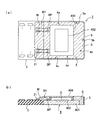
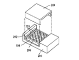
本実施の形態の固体撮像装置2は、図1に示すように、基板3と、固体撮像素子4と、枠体5とを備えている。なお、同図において、Mは封止樹脂部を示す。
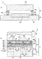
この固体撮像素子4は、図2(a)に断面図、図2(b)に要部拡大断面図を示すように、つまり前述したように、固体撮像素子基板4A表面に、シリコン基板401の受光領域に相当して空隙Cをもつようにスペーサ403を介してガラス基板404が接合されているとともに、シリコン基板401の周縁がダイシングによって個別に分離され、ガラス基板404から露呈する周縁部のシリコン基板401表面に形成されたボンディングパッドBPを介して、外部回路(図示せず)との電気的接続がなされるように構成されている。ここでスペーサ403は、10〜500μm、好ましくは80〜120μmの高さとする。
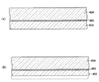
次に、同図(b)に示すように、適宜の手段、例えば周知のCMP(Chemical Mechanical Polishing;化学機械的研磨)法などによりシリコン基板403を所望の厚さまで薄片・平坦化させる。
即ち、本実施の形態では、初めに、同図(a)に示すように、シリコン基板403の全面にマスクレジストR1を塗布する。次に、所望のパターンを形成したフォトマスクF1(本実施の形態ではポジ型を使用するが、勿論、ネガ型でもよい)で露光を行い(同図(b))、その後、現像することにより、必要なスペーサに対応する部分を除く領域のマスクレジストR1を除去する(同図(c))。次に、ドライエッチングを行い、マスクレジストR1が塗布された領域以外のシリコン基板403及び接着剤層405を除去する(同図(d))。
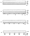
400はダイシングで形成される切断溝である。
即ち、初めに、図7に示す固体撮像素子4と基板3とを適宜の接着剤、例えば紫外線硬化型接着剤(例えば、カチオン重合性硬化接着剤)を用い、UV光源からの紫外線を照射して接合させる。次に、ワイヤボンダにより、固体撮像素子4側のボンディングパッドBPと基板3側の電極31とを金線などのボンディングワイヤBYで接続する。次に、ボンディングパッドBPと基板3側の電極31とを含む領域を絶縁性の樹脂、例えば熱硬化型エポキシ樹脂などにより被覆させ、絶縁性を確保した封止樹脂部Mを形成する(図1参照)。
また、本実施の形態によれば、固体撮像素子4の周囲の枠体5との間の隙間Sは耐湿性を持つ封止樹脂部Mで封止しており、固体撮像素子4について耐湿性を確保しているので、湿度や水分の多い場所で使用する場合であっても、電気的な故障や漏電などの虞がなく、信頼性の高いものが実現可能となる。しかも、本実施の形態では、固体撮像素子4の周囲の枠体5との間の隙間Sを封止する樹脂として、特に熱硬化型エポキシ樹脂を用いることで、その樹脂で封止された隙間部分は、硬化時に体積収縮が少なく、強度と強靱性に優れ、硬化後は溶剤そのほかに対する耐薬品性が非常によいなどの各種特性が得られるようになる。
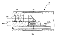
図8は本発明の第2の実施の形態に係る固体撮像装置を設けた直視型の電子内視鏡を示すものであり、この電子内視鏡は、内視鏡本体1の先端部10の内部に、第1の実施の形態の固体撮像装置2を設置している。
また、本実施の形態によれば、固体撮像素子4と基板3との間の電気的な接続部分の防水性とともに固体撮像素子4の耐湿性が得られるので、例えば生体観察用の内視鏡装置に用いる場合などには、電気的な故障や漏電などの虞がなく、信頼性を向上させることができる。
なお、本実施の形態では、固体撮像装置2を直視型の電子内視鏡に適用した構成であるが、勿論、側視型の電子内視鏡に適用することも勿論可能である。
10 先端部
11 観察窓
12 対物レンズ
13 プリズム
1A 観察チャンネル
14 鉗子孔
15 鉗子窓
2 固体撮像装置
3 基板
31 電極
4 固体撮像素子
4A 固体撮像素子基板
4B カバーガラス
4a〜4c (固体撮像素子の)外周面
400 切断溝
401 シリコン基板
402 固体撮像素子本体(本体部、CCD)
403 スペーサ
404 ガラス基板
405 接着剤層
446 フィルタ層
446R 赤色フィルタ層
446G 緑色フィルタ層
446B 青色フィルタ層
450 マイクロレンズ
5 枠体
5a〜5c (枠体の)内周面
BY ボンディングワイヤ(引出線)
BP ボンディンパッド
M 封止樹脂部
Claims (5)
- 固体撮像素子基板に固体撮像素子本体を搭載した固体撮像素子と、
一面に電極を設けた板状の基板であって、その一端面が前記固体撮像素子の一端面側に固着された板状の基板と、
前記板状の基板に接合一体化されるコの字形状の枠体と、
封止樹脂部と、を備え、
前記板状の基板の一面に設けた電極は、前記固体撮像素子の一面に設けられたパッドから引出したボンディングワイヤと電気的に接続されており、
前記枠体は、前記固体撮像素子の前記板状の基板に固着された一端面を除く外周面を囲設しており、
前記封止樹脂部は、前記板状の基板の前記一面の前記電極を含む所定部位から前記固体撮像素子の前記一面の前記パッドを含む所定部位に至るまでの領域を被覆している固体撮像装置。 - 請求項1に記載の固体撮像装置であって、
前記固体撮像素子と前記枠体との間には隙間が形成されているとともに、
前記固体撮像素子と前記枠体との間の前記隙間が耐湿性の樹脂で封止された固体撮像装置。 - 請求項2に記載の固体撮像装置であって、
前記樹脂は、熱硬化型エポキシ樹脂である固体撮像装置。 - 請求項1乃至3のいずれかに記載の固体撮像装置であって、
前記枠体は、金属板で構成された固体撮像装置。 - 請求項1乃至4のいずれかに記載の固体撮像装置を、内視鏡装置の先端内部又は先端側部に設けた電子内視鏡装置。
Priority Applications (5)
| Application Number | Priority Date | Filing Date | Title |
|---|---|---|---|
| JP2006027705A JP4834412B2 (ja) | 2006-02-03 | 2006-02-03 | 固体撮像装置およびこれを用いた電子内視鏡 |
| KR1020070010946A KR101286099B1 (ko) | 2006-02-03 | 2007-02-02 | 고체 촬상 장치 및 그것을 사용하는 전자 내시경 |
| EP07002297.5A EP1816678B1 (en) | 2006-02-03 | 2007-02-02 | Solid-state imaging device and electronic endoscope using the same |
| CN2007100080237A CN101013714B (zh) | 2006-02-03 | 2007-02-05 | 固态成像装置和使用其的电子内诊镜 |
| US11/702,221 US7692710B2 (en) | 2006-02-03 | 2007-02-05 | Solid-state imaging device and electronic endoscope using the same |
Applications Claiming Priority (1)
| Application Number | Priority Date | Filing Date | Title |
|---|---|---|---|
| JP2006027705A JP4834412B2 (ja) | 2006-02-03 | 2006-02-03 | 固体撮像装置およびこれを用いた電子内視鏡 |
Publications (3)
| Publication Number | Publication Date |
|---|---|
| JP2007202921A JP2007202921A (ja) | 2007-08-16 |
| JP2007202921A5 JP2007202921A5 (ja) | 2008-12-04 |
| JP4834412B2 true JP4834412B2 (ja) | 2011-12-14 |
Family
ID=37969721
Family Applications (1)
| Application Number | Title | Priority Date | Filing Date |
|---|---|---|---|
| JP2006027705A Expired - Lifetime JP4834412B2 (ja) | 2006-02-03 | 2006-02-03 | 固体撮像装置およびこれを用いた電子内視鏡 |
Country Status (5)
| Country | Link |
|---|---|
| US (1) | US7692710B2 (ja) |
| EP (1) | EP1816678B1 (ja) |
| JP (1) | JP4834412B2 (ja) |
| KR (1) | KR101286099B1 (ja) |
| CN (1) | CN101013714B (ja) |
Families Citing this family (74)
| Publication number | Priority date | Publication date | Assignee | Title |
|---|---|---|---|---|
| EP3328048B1 (en) | 2008-05-20 | 2021-04-21 | FotoNation Limited | Capturing and processing of images using monolithic camera array with heterogeneous imagers |
| US8866920B2 (en) | 2008-05-20 | 2014-10-21 | Pelican Imaging Corporation | Capturing and processing of images using monolithic camera array with heterogeneous imagers |
| US11792538B2 (en) | 2008-05-20 | 2023-10-17 | Adeia Imaging Llc | Capturing and processing of images including occlusions focused on an image sensor by a lens stack array |
| JP5532881B2 (ja) * | 2009-04-10 | 2014-06-25 | 株式会社リコー | 撮像装置、車載撮像装置、撮像装置の製造方法及び製造装置 |
| JP5453947B2 (ja) * | 2009-06-17 | 2014-03-26 | ソニー株式会社 | 固体撮像素子の製造方法 |
| JP5303414B2 (ja) * | 2009-09-25 | 2013-10-02 | 富士フイルム株式会社 | 撮像装置及び内視鏡 |
| EP2502115A4 (en) | 2009-11-20 | 2013-11-06 | Pelican Imaging Corp | RECORDING AND PROCESSING IMAGES THROUGH A MONOLITHIC CAMERA ARRAY WITH HETEROGENIC IMAGE CONVERTER |
| CN103004180A (zh) | 2010-05-12 | 2013-03-27 | 派力肯影像公司 | 成像器阵列和阵列照相机的架构 |
| US8878950B2 (en) | 2010-12-14 | 2014-11-04 | Pelican Imaging Corporation | Systems and methods for synthesizing high resolution images using super-resolution processes |
| JP5395829B2 (ja) * | 2011-02-25 | 2014-01-22 | 富士フイルム株式会社 | 内視鏡装置 |
| US8305456B1 (en) | 2011-05-11 | 2012-11-06 | Pelican Imaging Corporation | Systems and methods for transmitting and receiving array camera image data |
| CA2835870A1 (en) | 2011-05-12 | 2012-11-15 | Olive Medical Corporation | Pixel array area optimization using stacking scheme for hybrid image sensor with minimal vertical interconnects |
| US20130265459A1 (en) | 2011-06-28 | 2013-10-10 | Pelican Imaging Corporation | Optical arrangements for use with an array camera |
| WO2013043751A1 (en) | 2011-09-19 | 2013-03-28 | Pelican Imaging Corporation | Systems and methods for controlling aliasing in images captured by an array camera for use in super resolution processing using pixel apertures |
| CN104081414B (zh) | 2011-09-28 | 2017-08-01 | Fotonation开曼有限公司 | 用于编码和解码光场图像文件的系统及方法 |
| CN103239201A (zh) * | 2012-02-01 | 2013-08-14 | 恒景科技股份有限公司 | 具有光源的内视镜 |
| GB201202128D0 (en) | 2012-02-08 | 2012-03-21 | Univ Leeds | Novel material |
| US9412206B2 (en) | 2012-02-21 | 2016-08-09 | Pelican Imaging Corporation | Systems and methods for the manipulation of captured light field image data |
| US9210392B2 (en) | 2012-05-01 | 2015-12-08 | Pelican Imaging Coporation | Camera modules patterned with pi filter groups |
| JP5941753B2 (ja) * | 2012-05-28 | 2016-06-29 | 富士フイルム株式会社 | 電子内視鏡装置及び撮像モジュール並びに撮影レンズモールド方法 |
| EP2873028A4 (en) | 2012-06-28 | 2016-05-25 | Pelican Imaging Corp | SYSTEMS AND METHOD FOR DETECTING DEFECTIVE CAMERA ARRAYS, OPTICAL ARRAYS AND SENSORS |
| US20140002674A1 (en) | 2012-06-30 | 2014-01-02 | Pelican Imaging Corporation | Systems and Methods for Manufacturing Camera Modules Using Active Alignment of Lens Stack Arrays and Sensors |
| CN104486987A (zh) | 2012-07-26 | 2015-04-01 | 橄榄医疗公司 | 具有最小面积单片式cmos图像传感器的相机系统 |
| CN107346061B (zh) | 2012-08-21 | 2020-04-24 | 快图有限公司 | 用于使用阵列照相机捕捉的图像中的视差检测和校正的系统和方法 |
| EP2888698A4 (en) | 2012-08-23 | 2016-06-29 | Pelican Imaging Corp | PROPERTY-BASED HIGH-RESOLUTION MOTION ESTIMATION FROM LOW-RESOLUTION IMAGES RECORDED WITH AN ARRAY SOURCE |
| WO2014052974A2 (en) | 2012-09-28 | 2014-04-03 | Pelican Imaging Corporation | Generating images from light fields utilizing virtual viewpoints |
| US9143711B2 (en) | 2012-11-13 | 2015-09-22 | Pelican Imaging Corporation | Systems and methods for array camera focal plane control |
| JP6000859B2 (ja) * | 2013-01-11 | 2016-10-05 | オリンパス株式会社 | 半導体装置の製造方法、半導体装置、及び内視鏡 |
| US9462164B2 (en) | 2013-02-21 | 2016-10-04 | Pelican Imaging Corporation | Systems and methods for generating compressed light field representation data using captured light fields, array geometry, and parallax information |
| US9253380B2 (en) | 2013-02-24 | 2016-02-02 | Pelican Imaging Corporation | Thin form factor computational array cameras and modular array cameras |
| US9774789B2 (en) | 2013-03-08 | 2017-09-26 | Fotonation Cayman Limited | Systems and methods for high dynamic range imaging using array cameras |
| US8866912B2 (en) | 2013-03-10 | 2014-10-21 | Pelican Imaging Corporation | System and methods for calibration of an array camera using a single captured image |
| US9106784B2 (en) | 2013-03-13 | 2015-08-11 | Pelican Imaging Corporation | Systems and methods for controlling aliasing in images captured by an array camera for use in super-resolution processing |
| US9519972B2 (en) | 2013-03-13 | 2016-12-13 | Kip Peli P1 Lp | Systems and methods for synthesizing images from image data captured by an array camera using restricted depth of field depth maps in which depth estimation precision varies |
| US9888194B2 (en) | 2013-03-13 | 2018-02-06 | Fotonation Cayman Limited | Array camera architecture implementing quantum film image sensors |
| US9124831B2 (en) | 2013-03-13 | 2015-09-01 | Pelican Imaging Corporation | System and methods for calibration of an array camera |
| WO2014159779A1 (en) | 2013-03-14 | 2014-10-02 | Pelican Imaging Corporation | Systems and methods for reducing motion blur in images or video in ultra low light with array cameras |
| WO2014153098A1 (en) | 2013-03-14 | 2014-09-25 | Pelican Imaging Corporation | Photmetric normalization in array cameras |
| US9445003B1 (en) | 2013-03-15 | 2016-09-13 | Pelican Imaging Corporation | Systems and methods for synthesizing high resolution images using image deconvolution based on motion and depth information |
| AU2014233192B2 (en) | 2013-03-15 | 2018-11-22 | DePuy Synthes Products, Inc. | Minimize image sensor I/O and conductor counts in endoscope applications |
| EP4604059A3 (en) | 2013-03-15 | 2025-09-17 | Adeia Imaging LLC | Systems and methods for stereo imaging with camera arrays |
| WO2014145246A1 (en) | 2013-03-15 | 2014-09-18 | Olive Medical Corporation | Image sensor synchronization without input clock and data transmission clock |
| US10122993B2 (en) | 2013-03-15 | 2018-11-06 | Fotonation Limited | Autofocus system for a conventional camera that uses depth information from an array camera |
| US9497429B2 (en) | 2013-03-15 | 2016-11-15 | Pelican Imaging Corporation | Extended color processing on pelican array cameras |
| WO2015048694A2 (en) | 2013-09-27 | 2015-04-02 | Pelican Imaging Corporation | Systems and methods for depth-assisted perspective distortion correction |
| US9426343B2 (en) | 2013-11-07 | 2016-08-23 | Pelican Imaging Corporation | Array cameras incorporating independently aligned lens stacks |
| US10119808B2 (en) | 2013-11-18 | 2018-11-06 | Fotonation Limited | Systems and methods for estimating depth from projected texture using camera arrays |
| EP3075140B1 (en) | 2013-11-26 | 2018-06-13 | FotoNation Cayman Limited | Array camera configurations incorporating multiple constituent array cameras |
| US10089740B2 (en) | 2014-03-07 | 2018-10-02 | Fotonation Limited | System and methods for depth regularization and semiautomatic interactive matting using RGB-D images |
| US9521319B2 (en) * | 2014-06-18 | 2016-12-13 | Pelican Imaging Corporation | Array cameras and array camera modules including spectral filters disposed outside of a constituent image sensor |
| CN113256730B (zh) | 2014-09-29 | 2023-09-05 | 快图有限公司 | 用于阵列相机的动态校准的系统和方法 |
| KR101652420B1 (ko) | 2014-12-17 | 2016-09-09 | 주식회사 포스코 | 래들의 슬라이드 게이트 개폐 상태 알림 장치 |
| WO2016117119A1 (ja) * | 2015-01-23 | 2016-07-28 | オリンパス株式会社 | 撮像装置および内視鏡 |
| US9942474B2 (en) | 2015-04-17 | 2018-04-10 | Fotonation Cayman Limited | Systems and methods for performing high speed video capture and depth estimation using array cameras |
| CN204760384U (zh) * | 2015-05-18 | 2015-11-11 | 华天科技(昆山)电子有限公司 | 高像素影像传感芯片的晶圆级封装结构 |
| JP2017175004A (ja) * | 2016-03-24 | 2017-09-28 | ソニー株式会社 | チップサイズパッケージ、製造方法、電子機器、および内視鏡 |
| US10482618B2 (en) | 2017-08-21 | 2019-11-19 | Fotonation Limited | Systems and methods for hybrid depth regularization |
| WO2021055585A1 (en) | 2019-09-17 | 2021-03-25 | Boston Polarimetrics, Inc. | Systems and methods for surface modeling using polarization cues |
| WO2021071995A1 (en) | 2019-10-07 | 2021-04-15 | Boston Polarimetrics, Inc. | Systems and methods for surface normals sensing with polarization |
| EP4066001B1 (en) | 2019-11-30 | 2026-03-04 | Intrinsic Innovation LLC | Systems and methods for transparent object segmentation using polarization cues |
| JP7462769B2 (ja) | 2020-01-29 | 2024-04-05 | イントリンジック イノベーション エルエルシー | 物体の姿勢の検出および測定システムを特徴付けるためのシステムおよび方法 |
| US11797863B2 (en) | 2020-01-30 | 2023-10-24 | Intrinsic Innovation Llc | Systems and methods for synthesizing data for training statistical models on different imaging modalities including polarized images |
| WO2021243088A1 (en) | 2020-05-27 | 2021-12-02 | Boston Polarimetrics, Inc. | Multi-aperture polarization optical systems using beam splitters |
| TWI818199B (zh) | 2020-10-06 | 2023-10-11 | 友達光電股份有限公司 | 發光裝置及其製造方法 |
| US12069227B2 (en) | 2021-03-10 | 2024-08-20 | Intrinsic Innovation Llc | Multi-modal and multi-spectral stereo camera arrays |
| US12020455B2 (en) | 2021-03-10 | 2024-06-25 | Intrinsic Innovation Llc | Systems and methods for high dynamic range image reconstruction |
| US11954886B2 (en) | 2021-04-15 | 2024-04-09 | Intrinsic Innovation Llc | Systems and methods for six-degree of freedom pose estimation of deformable objects |
| US11290658B1 (en) | 2021-04-15 | 2022-03-29 | Boston Polarimetrics, Inc. | Systems and methods for camera exposure control |
| US12067746B2 (en) | 2021-05-07 | 2024-08-20 | Intrinsic Innovation Llc | Systems and methods for using computer vision to pick up small objects |
| US12175741B2 (en) | 2021-06-22 | 2024-12-24 | Intrinsic Innovation Llc | Systems and methods for a vision guided end effector |
| US12340538B2 (en) | 2021-06-25 | 2025-06-24 | Intrinsic Innovation Llc | Systems and methods for generating and using visual datasets for training computer vision models |
| US12172310B2 (en) | 2021-06-29 | 2024-12-24 | Intrinsic Innovation Llc | Systems and methods for picking objects using 3-D geometry and segmentation |
| US11689813B2 (en) | 2021-07-01 | 2023-06-27 | Intrinsic Innovation Llc | Systems and methods for high dynamic range imaging using crossed polarizers |
| US12293535B2 (en) | 2021-08-03 | 2025-05-06 | Intrinsic Innovation Llc | Systems and methods for training pose estimators in computer vision |
Family Cites Families (12)
| Publication number | Priority date | Publication date | Assignee | Title |
|---|---|---|---|---|
| US4918521A (en) * | 1987-01-20 | 1990-04-17 | Olympus Optical Co., Ltd. | Solid state imaging apparatus |
| JP3216650B2 (ja) * | 1990-08-27 | 2001-10-09 | オリンパス光学工業株式会社 | 固体撮像装置 |
| JP3065378B2 (ja) | 1991-04-26 | 2000-07-17 | 富士写真光機株式会社 | 電子内視鏡用固体撮像素子の回路基板 |
| JP2544978Y2 (ja) * | 1991-06-06 | 1997-08-20 | 住友電気工業株式会社 | 光モジュール |
| JP2694750B2 (ja) | 1991-07-10 | 1997-12-24 | 富士写真光機株式会社 | 固体撮像素子パッケージ |
| DE4129961C2 (de) * | 1991-09-10 | 1996-02-15 | Wolf Gmbh Richard | Videoendoskop mit Festkörperbildaufnahmevorrichtung |
| JP3364574B2 (ja) * | 1997-02-07 | 2003-01-08 | 富士写真光機株式会社 | 内視鏡用撮像装置 |
| JPH1199126A (ja) * | 1997-09-29 | 1999-04-13 | Olympus Optical Co Ltd | 電子内視鏡 |
| US6350990B1 (en) * | 1999-11-04 | 2002-02-26 | General Electric Company | End cap and sealing method for imager |
| JP2002231918A (ja) * | 2001-02-06 | 2002-08-16 | Olympus Optical Co Ltd | 固体撮像装置及びその製造方法 |
| JP4551638B2 (ja) * | 2003-08-01 | 2010-09-29 | 富士フイルム株式会社 | 固体撮像装置の製造方法 |
| US20060164510A1 (en) * | 2005-01-24 | 2006-07-27 | Doron Adler | Sensor with narrow mounting profile |
-
2006
- 2006-02-03 JP JP2006027705A patent/JP4834412B2/ja not_active Expired - Lifetime
-
2007
- 2007-02-02 KR KR1020070010946A patent/KR101286099B1/ko not_active Expired - Fee Related
- 2007-02-02 EP EP07002297.5A patent/EP1816678B1/en not_active Not-in-force
- 2007-02-05 US US11/702,221 patent/US7692710B2/en active Active
- 2007-02-05 CN CN2007100080237A patent/CN101013714B/zh not_active Expired - Fee Related
Also Published As
| Publication number | Publication date |
|---|---|
| US20070182843A1 (en) | 2007-08-09 |
| KR20070079931A (ko) | 2007-08-08 |
| KR101286099B1 (ko) | 2013-07-15 |
| EP1816678B1 (en) | 2014-06-25 |
| CN101013714B (zh) | 2010-05-19 |
| EP1816678A2 (en) | 2007-08-08 |
| EP1816678A3 (en) | 2010-05-26 |
| JP2007202921A (ja) | 2007-08-16 |
| CN101013714A (zh) | 2007-08-08 |
| US7692710B2 (en) | 2010-04-06 |
Similar Documents
| Publication | Publication Date | Title |
|---|---|---|
| JP4834412B2 (ja) | 固体撮像装置およびこれを用いた電子内視鏡 | |
| US7898085B2 (en) | Solid-state imaging device and manufacturing method thereof | |
| US7074638B2 (en) | Solid-state imaging device and method of manufacturing said solid-state imaging device | |
| US20080303107A1 (en) | Optical device and method for fabricating the same, camera module using optical device, and electronic equipment mounting camera module | |
| TWI800487B (zh) | 固體攝像元件及製造方法、以及電子機器 | |
| EP1990829A2 (en) | Solid-state imaging device and method of manufacturing the same | |
| JP4660259B2 (ja) | 半導体装置の製造方法 | |
| JP4486005B2 (ja) | 半導体撮像装置およびその製造方法 | |
| JP2003347529A (ja) | 固体撮像装置およびその製造方法 | |
| JP2004063782A (ja) | 固体撮像装置およびその製造方法 | |
| JP4865267B2 (ja) | 固体撮像装置及び内視鏡 | |
| JP2011199036A (ja) | 固体撮像装置及びその製造方法 | |
| JP2007123351A (ja) | 固体撮像装置 | |
| JP2022134124A (ja) | 画像キャプチャモジュール、撮像ユニット、内視鏡、及び画像キャプチャモジュールの製造方法 | |
| JP4739697B2 (ja) | 固体撮像素子及び内視鏡 | |
| JP2004063772A (ja) | 固体撮像装置およびその製造方法 | |
| JP2009111130A (ja) | 撮像装置及びその製造方法 | |
| JP2006216657A (ja) | 固体撮像装置及び光学モジュール | |
| JP2012090033A (ja) | 撮像モジュール | |
| JP2008219262A (ja) | 撮像モジュール | |
| JP2006216656A (ja) | 半導体装置 |
Legal Events
| Date | Code | Title | Description |
|---|---|---|---|
| RD04 | Notification of resignation of power of attorney |
Free format text: JAPANESE INTERMEDIATE CODE: A7424 Effective date: 20071112 |
|
| RD04 | Notification of resignation of power of attorney |
Free format text: JAPANESE INTERMEDIATE CODE: A7424 Effective date: 20071119 |
|
| RD04 | Notification of resignation of power of attorney |
Free format text: JAPANESE INTERMEDIATE CODE: A7424 Effective date: 20071127 |
|
| A521 | Request for written amendment filed |
Free format text: JAPANESE INTERMEDIATE CODE: A523 Effective date: 20081021 |
|
| A621 | Written request for application examination |
Free format text: JAPANESE INTERMEDIATE CODE: A621 Effective date: 20081021 |
|
| A711 | Notification of change in applicant |
Free format text: JAPANESE INTERMEDIATE CODE: A711 Effective date: 20100618 |
|
| A131 | Notification of reasons for refusal |
Free format text: JAPANESE INTERMEDIATE CODE: A131 Effective date: 20110524 |
|
| A977 | Report on retrieval |
Free format text: JAPANESE INTERMEDIATE CODE: A971007 Effective date: 20110526 |
|
| A521 | Request for written amendment filed |
Free format text: JAPANESE INTERMEDIATE CODE: A523 Effective date: 20110621 |
|
| RD03 | Notification of appointment of power of attorney |
Free format text: JAPANESE INTERMEDIATE CODE: A7423 Effective date: 20110707 |
|
| TRDD | Decision of grant or rejection written | ||
| A01 | Written decision to grant a patent or to grant a registration (utility model) |
Free format text: JAPANESE INTERMEDIATE CODE: A01 Effective date: 20110830 |
|
| A01 | Written decision to grant a patent or to grant a registration (utility model) |
Free format text: JAPANESE INTERMEDIATE CODE: A01 |
|
| A61 | First payment of annual fees (during grant procedure) |
Free format text: JAPANESE INTERMEDIATE CODE: A61 Effective date: 20110926 |
|
| R150 | Certificate of patent or registration of utility model |
Ref document number: 4834412 Country of ref document: JP Free format text: JAPANESE INTERMEDIATE CODE: R150 Free format text: JAPANESE INTERMEDIATE CODE: R150 |
|
| FPAY | Renewal fee payment (event date is renewal date of database) |
Free format text: PAYMENT UNTIL: 20140930 Year of fee payment: 3 |
|
| R250 | Receipt of annual fees |
Free format text: JAPANESE INTERMEDIATE CODE: R250 |
|
| R250 | Receipt of annual fees |
Free format text: JAPANESE INTERMEDIATE CODE: R250 |
|
| R250 | Receipt of annual fees |
Free format text: JAPANESE INTERMEDIATE CODE: R250 |
|
| R250 | Receipt of annual fees |
Free format text: JAPANESE INTERMEDIATE CODE: R250 |
|
| R250 | Receipt of annual fees |
Free format text: JAPANESE INTERMEDIATE CODE: R250 |
|
| R250 | Receipt of annual fees |
Free format text: JAPANESE INTERMEDIATE CODE: R250 |
|
| R250 | Receipt of annual fees |
Free format text: JAPANESE INTERMEDIATE CODE: R250 |
|
| R250 | Receipt of annual fees |
Free format text: JAPANESE INTERMEDIATE CODE: R250 |
|
| R250 | Receipt of annual fees |
Free format text: JAPANESE INTERMEDIATE CODE: R250 |
|
| R250 | Receipt of annual fees |
Free format text: JAPANESE INTERMEDIATE CODE: R250 |
|
| R250 | Receipt of annual fees |
Free format text: JAPANESE INTERMEDIATE CODE: R250 |