JP4687534B2 - Substrate mounting mechanism and substrate processing apparatus - Google Patents
Substrate mounting mechanism and substrate processing apparatus Download PDFInfo
- Publication number
- JP4687534B2 JP4687534B2 JP2006095167A JP2006095167A JP4687534B2 JP 4687534 B2 JP4687534 B2 JP 4687534B2 JP 2006095167 A JP2006095167 A JP 2006095167A JP 2006095167 A JP2006095167 A JP 2006095167A JP 4687534 B2 JP4687534 B2 JP 4687534B2
- Authority
- JP
- Japan
- Prior art keywords
- pin
- lifter
- lifter pin
- substrate
- sleeve
- Prior art date
- Legal status (The legal status is an assumption and is not a legal conclusion. Google has not performed a legal analysis and makes no representation as to the accuracy of the status listed.)
- Expired - Fee Related
Links
- 238000012545 processing Methods 0.000 title claims description 73
- 239000000758 substrate Substances 0.000 title claims description 56
- 230000007246 mechanism Effects 0.000 title claims description 55
- 238000003780 insertion Methods 0.000 claims description 38
- 230000037431 insertion Effects 0.000 claims description 38
- 238000000034 method Methods 0.000 claims description 9
- 239000007789 gas Substances 0.000 description 69
- 235000012431 wafers Nutrition 0.000 description 42
- 239000010408 film Substances 0.000 description 17
- 238000012546 transfer Methods 0.000 description 13
- 229910003074 TiCl4 Inorganic materials 0.000 description 8
- XJDNKRIXUMDJCW-UHFFFAOYSA-J titanium tetrachloride Chemical compound Cl[Ti](Cl)(Cl)Cl XJDNKRIXUMDJCW-UHFFFAOYSA-J 0.000 description 8
- 230000002093 peripheral effect Effects 0.000 description 7
- 238000004140 cleaning Methods 0.000 description 6
- 239000002245 particle Substances 0.000 description 6
- 239000007795 chemical reaction product Substances 0.000 description 5
- 238000005229 chemical vapour deposition Methods 0.000 description 5
- QGZKDVFQNNGYKY-UHFFFAOYSA-N Ammonia Chemical compound N QGZKDVFQNNGYKY-UHFFFAOYSA-N 0.000 description 4
- 238000005530 etching Methods 0.000 description 4
- 238000012423 maintenance Methods 0.000 description 4
- 238000000151 deposition Methods 0.000 description 3
- 230000008021 deposition Effects 0.000 description 3
- 238000010586 diagram Methods 0.000 description 3
- 238000009825 accumulation Methods 0.000 description 2
- PNEYBMLMFCGWSK-UHFFFAOYSA-N aluminium oxide Inorganic materials [O-2].[O-2].[O-2].[Al+3].[Al+3] PNEYBMLMFCGWSK-UHFFFAOYSA-N 0.000 description 2
- 238000010438 heat treatment Methods 0.000 description 2
- 239000000463 material Substances 0.000 description 2
- 239000007787 solid Substances 0.000 description 2
- 239000010936 titanium Substances 0.000 description 2
- ATJFFYVFTNAWJD-UHFFFAOYSA-N Tin Chemical compound [Sn] ATJFFYVFTNAWJD-UHFFFAOYSA-N 0.000 description 1
- RTAQQCXQSZGOHL-UHFFFAOYSA-N Titanium Chemical compound [Ti] RTAQQCXQSZGOHL-UHFFFAOYSA-N 0.000 description 1
- 230000002159 abnormal effect Effects 0.000 description 1
- XAGFODPZIPBFFR-UHFFFAOYSA-N aluminium Chemical compound [Al] XAGFODPZIPBFFR-UHFFFAOYSA-N 0.000 description 1
- 229910052782 aluminium Inorganic materials 0.000 description 1
- 229910021529 ammonia Inorganic materials 0.000 description 1
- 230000004323 axial length Effects 0.000 description 1
- 239000012141 concentrate Substances 0.000 description 1
- 238000011109 contamination Methods 0.000 description 1
- 238000005137 deposition process Methods 0.000 description 1
- 230000006866 deterioration Effects 0.000 description 1
- 230000000694 effects Effects 0.000 description 1
- 230000003028 elevating effect Effects 0.000 description 1
- 239000011159 matrix material Substances 0.000 description 1
- 239000004570 mortar (masonry) Substances 0.000 description 1
- 229910000069 nitrogen hydride Inorganic materials 0.000 description 1
- 238000005268 plasma chemical vapour deposition Methods 0.000 description 1
- 239000013049 sediment Substances 0.000 description 1
- 239000004065 semiconductor Substances 0.000 description 1
- 239000010409 thin film Substances 0.000 description 1
- 229910052719 titanium Inorganic materials 0.000 description 1
- 230000007704 transition Effects 0.000 description 1
- 230000007723 transport mechanism Effects 0.000 description 1
Images


Classifications
-
- C—CHEMISTRY; METALLURGY
- C23—COATING METALLIC MATERIAL; COATING MATERIAL WITH METALLIC MATERIAL; CHEMICAL SURFACE TREATMENT; DIFFUSION TREATMENT OF METALLIC MATERIAL; COATING BY VACUUM EVAPORATION, BY SPUTTERING, BY ION IMPLANTATION OR BY CHEMICAL VAPOUR DEPOSITION, IN GENERAL; INHIBITING CORROSION OF METALLIC MATERIAL OR INCRUSTATION IN GENERAL
- C23C—COATING METALLIC MATERIAL; COATING MATERIAL WITH METALLIC MATERIAL; SURFACE TREATMENT OF METALLIC MATERIAL BY DIFFUSION INTO THE SURFACE, BY CHEMICAL CONVERSION OR SUBSTITUTION; COATING BY VACUUM EVAPORATION, BY SPUTTERING, BY ION IMPLANTATION OR BY CHEMICAL VAPOUR DEPOSITION, IN GENERAL
- C23C8/00—Solid state diffusion of only non-metal elements into metallic material surfaces; Chemical surface treatment of metallic material by reaction of the surface with a reactive gas, leaving reaction products of surface material in the coating, e.g. conversion coatings, passivation of metals
-
- C—CHEMISTRY; METALLURGY
- C23—COATING METALLIC MATERIAL; COATING MATERIAL WITH METALLIC MATERIAL; CHEMICAL SURFACE TREATMENT; DIFFUSION TREATMENT OF METALLIC MATERIAL; COATING BY VACUUM EVAPORATION, BY SPUTTERING, BY ION IMPLANTATION OR BY CHEMICAL VAPOUR DEPOSITION, IN GENERAL; INHIBITING CORROSION OF METALLIC MATERIAL OR INCRUSTATION IN GENERAL
- C23C—COATING METALLIC MATERIAL; COATING MATERIAL WITH METALLIC MATERIAL; SURFACE TREATMENT OF METALLIC MATERIAL BY DIFFUSION INTO THE SURFACE, BY CHEMICAL CONVERSION OR SUBSTITUTION; COATING BY VACUUM EVAPORATION, BY SPUTTERING, BY ION IMPLANTATION OR BY CHEMICAL VAPOUR DEPOSITION, IN GENERAL
- C23C10/00—Solid state diffusion of only metal elements or silicon into metallic material surfaces
-
- C—CHEMISTRY; METALLURGY
- C23—COATING METALLIC MATERIAL; COATING MATERIAL WITH METALLIC MATERIAL; CHEMICAL SURFACE TREATMENT; DIFFUSION TREATMENT OF METALLIC MATERIAL; COATING BY VACUUM EVAPORATION, BY SPUTTERING, BY ION IMPLANTATION OR BY CHEMICAL VAPOUR DEPOSITION, IN GENERAL; INHIBITING CORROSION OF METALLIC MATERIAL OR INCRUSTATION IN GENERAL
- C23C—COATING METALLIC MATERIAL; COATING MATERIAL WITH METALLIC MATERIAL; SURFACE TREATMENT OF METALLIC MATERIAL BY DIFFUSION INTO THE SURFACE, BY CHEMICAL CONVERSION OR SUBSTITUTION; COATING BY VACUUM EVAPORATION, BY SPUTTERING, BY ION IMPLANTATION OR BY CHEMICAL VAPOUR DEPOSITION, IN GENERAL
- C23C16/00—Chemical coating by decomposition of gaseous compounds, without leaving reaction products of surface material in the coating, i.e. chemical vapour deposition [CVD] processes
- C23C16/44—Chemical coating by decomposition of gaseous compounds, without leaving reaction products of surface material in the coating, i.e. chemical vapour deposition [CVD] processes characterised by the method of coating
- C23C16/4401—Means for minimising impurities, e.g. dust, moisture or residual gas, in the reaction chamber
-
- C—CHEMISTRY; METALLURGY
- C23—COATING METALLIC MATERIAL; COATING MATERIAL WITH METALLIC MATERIAL; CHEMICAL SURFACE TREATMENT; DIFFUSION TREATMENT OF METALLIC MATERIAL; COATING BY VACUUM EVAPORATION, BY SPUTTERING, BY ION IMPLANTATION OR BY CHEMICAL VAPOUR DEPOSITION, IN GENERAL; INHIBITING CORROSION OF METALLIC MATERIAL OR INCRUSTATION IN GENERAL
- C23C—COATING METALLIC MATERIAL; COATING MATERIAL WITH METALLIC MATERIAL; SURFACE TREATMENT OF METALLIC MATERIAL BY DIFFUSION INTO THE SURFACE, BY CHEMICAL CONVERSION OR SUBSTITUTION; COATING BY VACUUM EVAPORATION, BY SPUTTERING, BY ION IMPLANTATION OR BY CHEMICAL VAPOUR DEPOSITION, IN GENERAL
- C23C16/00—Chemical coating by decomposition of gaseous compounds, without leaving reaction products of surface material in the coating, i.e. chemical vapour deposition [CVD] processes
- C23C16/44—Chemical coating by decomposition of gaseous compounds, without leaving reaction products of surface material in the coating, i.e. chemical vapour deposition [CVD] processes characterised by the method of coating
- C23C16/458—Chemical coating by decomposition of gaseous compounds, without leaving reaction products of surface material in the coating, i.e. chemical vapour deposition [CVD] processes characterised by the method of coating characterised by the method used for supporting substrates in the reaction chamber
- C23C16/4582—Rigid and flat substrates, e.g. plates or discs
- C23C16/4583—Rigid and flat substrates, e.g. plates or discs the substrate being supported substantially horizontally
- C23C16/4586—Elements in the interior of the support, e.g. electrodes, heating or cooling devices
-
- H—ELECTRICITY
- H01—ELECTRIC ELEMENTS
- H01L—SEMICONDUCTOR DEVICES NOT COVERED BY CLASS H10
- H01L21/00—Processes or apparatus adapted for the manufacture or treatment of semiconductor or solid state devices or of parts thereof
- H01L21/67—Apparatus specially adapted for handling semiconductor or electric solid state devices during manufacture or treatment thereof; Apparatus specially adapted for handling wafers during manufacture or treatment of semiconductor or electric solid state devices or components ; Apparatus not specifically provided for elsewhere
- H01L21/683—Apparatus specially adapted for handling semiconductor or electric solid state devices during manufacture or treatment thereof; Apparatus specially adapted for handling wafers during manufacture or treatment of semiconductor or electric solid state devices or components ; Apparatus not specifically provided for elsewhere for supporting or gripping
- H01L21/687—Apparatus specially adapted for handling semiconductor or electric solid state devices during manufacture or treatment thereof; Apparatus specially adapted for handling wafers during manufacture or treatment of semiconductor or electric solid state devices or components ; Apparatus not specifically provided for elsewhere for supporting or gripping using mechanical means, e.g. chucks, clamps or pinches
- H01L21/68714—Apparatus specially adapted for handling semiconductor or electric solid state devices during manufacture or treatment thereof; Apparatus specially adapted for handling wafers during manufacture or treatment of semiconductor or electric solid state devices or components ; Apparatus not specifically provided for elsewhere for supporting or gripping using mechanical means, e.g. chucks, clamps or pinches the wafers being placed on a susceptor, stage or support
- H01L21/68742—Apparatus specially adapted for handling semiconductor or electric solid state devices during manufacture or treatment thereof; Apparatus specially adapted for handling wafers during manufacture or treatment of semiconductor or electric solid state devices or components ; Apparatus not specifically provided for elsewhere for supporting or gripping using mechanical means, e.g. chucks, clamps or pinches the wafers being placed on a susceptor, stage or support characterised by a lifting arrangement, e.g. lift pins
-
- H—ELECTRICITY
- H01—ELECTRIC ELEMENTS
- H01L—SEMICONDUCTOR DEVICES NOT COVERED BY CLASS H10
- H01L21/00—Processes or apparatus adapted for the manufacture or treatment of semiconductor or solid state devices or of parts thereof
- H01L21/67—Apparatus specially adapted for handling semiconductor or electric solid state devices during manufacture or treatment thereof; Apparatus specially adapted for handling wafers during manufacture or treatment of semiconductor or electric solid state devices or components ; Apparatus not specifically provided for elsewhere
- H01L21/683—Apparatus specially adapted for handling semiconductor or electric solid state devices during manufacture or treatment thereof; Apparatus specially adapted for handling wafers during manufacture or treatment of semiconductor or electric solid state devices or components ; Apparatus not specifically provided for elsewhere for supporting or gripping
- H01L21/687—Apparatus specially adapted for handling semiconductor or electric solid state devices during manufacture or treatment thereof; Apparatus specially adapted for handling wafers during manufacture or treatment of semiconductor or electric solid state devices or components ; Apparatus not specifically provided for elsewhere for supporting or gripping using mechanical means, e.g. chucks, clamps or pinches
- H01L21/68714—Apparatus specially adapted for handling semiconductor or electric solid state devices during manufacture or treatment thereof; Apparatus specially adapted for handling wafers during manufacture or treatment of semiconductor or electric solid state devices or components ; Apparatus not specifically provided for elsewhere for supporting or gripping using mechanical means, e.g. chucks, clamps or pinches the wafers being placed on a susceptor, stage or support
- H01L21/68785—Apparatus specially adapted for handling semiconductor or electric solid state devices during manufacture or treatment thereof; Apparatus specially adapted for handling wafers during manufacture or treatment of semiconductor or electric solid state devices or components ; Apparatus not specifically provided for elsewhere for supporting or gripping using mechanical means, e.g. chucks, clamps or pinches the wafers being placed on a susceptor, stage or support characterised by the mechanical construction of the susceptor, stage or support
Description
本発明は、被処理基板を載置する載置台を備え、昇降機構を介して昇降するリフタピンにより被処理基板を昇降させる基板の載置機構及びこの載置機構を備えた基板処理装置に関する。 The present invention relates to a substrate mounting mechanism that includes a mounting table on which a substrate to be processed is mounted, and that lifts and lowers the substrate to be processed by lifter pins that are lifted and lowered via a lifting mechanism, and a substrate processing apparatus that includes this mounting mechanism.
一般に被処理基板例えば半導体ウエハ(以下ウエハとする)にCVD(Chemical Vapor Deposition)による成膜処理やエッチング処理などの各種の処理を行う装置は、内部にウエハに対して処理を行う処理ガスが供給される処理容器を備えており、また処理容器の内部には処理が行われるウエハを載置するための載置台を備えた載置機構が設けられる。この載置機構は載置台と、ウエハを処理容器内に搬送する搬送機構(不図示)との間でウエハの受け渡しを行う役割を有している。 In general, an apparatus for performing various processes such as a film deposition process and an etching process by CVD (Chemical Vapor Deposition) on a substrate to be processed such as a semiconductor wafer (hereinafter referred to as a wafer) is supplied with a processing gas for processing the wafer. In addition, a mounting mechanism including a mounting table for mounting a wafer to be processed is provided inside the processing container. This mounting mechanism has a role of delivering a wafer between the mounting table and a transfer mechanism (not shown) that transfers the wafer into the processing container.
この従来のウエハの載置機構1について図9を用いて説明する。図中11は載置台であり、12はその載置台11におけるウエハWの載置面である。例えばその載置台11にはその周方向に沿って、間隔をおくように3つの貫通孔が鉛直方向に向かって穿孔されている。各貫通孔にはスリーブ13が嵌合、固定されている。スリーブ13内にはリフタピン15が挿入されていると共に、リフタピン15の下方にはピンベース16が設けられており、ピンベース16はリフタアーム17を介して不図示の駆動部に接続されている。リフタピン15がウエハWの受け渡しを行っていないときには、図9(a)に示すようにリフタピン15の上端は載置台11の載置面12の下方に位置しており、この位置をホームポジションと呼ぶことにすると、この載置機構1が搬送機構からウエハWを受け取る際にはリフタアーム17の上昇によりピンベース16が、ホームポジションにある各リフタピン15を鉛直方向に押し上げることで、図9(b)に示すようにリフタピン15が載置台11上に突出する。そしてこの突出したリフタピン15が搬送機構により処理容器内に搬入されたウエハWの裏面を支持し、その後ピンベース16が下降し、そのピンベース16の下降に従ってリフタピン15がウエハWを支持したまま下降して前記ホームポジションに戻り、これによりウエハWが載置台11上に載置されるようになっている。なおスリーブ13内をリフタピン15がスムーズに昇降するためにスリーブ13の内壁とリフタピン15との間にはある程度の大きさの隙間が設けられており、このリフタピン15は、その一部をスリーブ13の内壁に接触させながらスリーブ内を昇降するようになっている。
The conventional wafer mounting mechanism 1 will be described with reference to FIG. In the figure, 11 is a mounting table, and 12 is a mounting surface of the wafer W on the mounting table 11. For example, the mounting table 11 has three through holes drilled in the vertical direction so as to be spaced along the circumferential direction. A
しかし既述の従来の載置機構には以下に説明するような問題がある。例えばCVDによって導電膜であるTi(チタン)膜をウエハWに形成するための成膜装置において、ウエハWをこの成膜装置の処理容器内に搬送し、載置台11に載置した後に成膜ガスであるTiCl4ガスを処理容器内に供給した場合、そのTiCl4ガスの一部は載置台11の下面に回り込む。TiCl4ガスは固体間の隙間に流入し、その隙間においてデポ物(堆積物)を形成しやすいという特徴があるため、このTiCl4ガスは、図10(a)に矢印で示すように載置台11の下部から前記リフタピン15とスリーブ13との隙間に進入し、図10(b)に示すようにこの隙間を塞ぐようにデポ物(堆積物)19が形成される場合がある。このようにデポ物19が形成され、蓄積するとリフタピン15がスリーブ13内をスムーズに動くことができなくてホームポジションまで降りなくなり、あるいはスリーブ13に固着され、そしてこのような状態でピンベース16により無理に持ち上げられると、リフタピン15が折れてしまうおそれがある。
またCVDによる成膜装置はプラズマを利用する場合があるが、リフタピン15とスリーブ13との隙間に前記TiCl4などのガスから生成した導電性のデポ物19が付着すると、処理容器内にプラズマが発生した場合にリフタピン15の電位と載置台11の電位との間に差が生じることによってリフタピン15の周囲に異常放電が起こり、リフタピン15が劣化することによりその破損が助長される懸念もある。
However, the above-described conventional mounting mechanism has the following problems. For example, in a film forming apparatus for forming a Ti (titanium) film as a conductive film on a wafer W by CVD, the wafer W is transferred into a processing container of the film forming apparatus and mounted on the mounting table 11. When TiCl4 gas, which is a gas, is supplied into the processing container, a part of the TiCl4 gas goes around the lower surface of the mounting table 11. Since TiCl4 gas flows into gaps between solids and deposits (sediments) are easily formed in the gaps, this TiCl4 gas has a characteristic of the mounting table 11 as shown by an arrow in FIG. In some cases, a deposit (deposit) 19 is formed so as to enter the gap between the
In addition, a film forming apparatus using CVD may use plasma, but if
ところで既述のように成膜ガスから生成したデポ物19がリフタピン15とスリーブ13との隙間を塞ぐ現象は上述のプロセスに限られるものではないし、またエッチング装置の載置機構についても例えばエッチングによる反応生成物の粒子が前記隙間に詰まり、同様の不具合を発生させる場合がある。
By the way, as described above, the phenomenon in which the
このような成膜装置やエッチング装置に設けられた載置機構におけるリフタピン15の破損を防ぐためには、短期間で当該リフタピン15及びスリーブ13の煩雑な交換作業やこれらの部品のクリーニングを強いられ、メンテナンス作業の負担が大きくなる要因の一つとなっていた。
In order to prevent breakage of the
なお特許文献1にはピン挿入孔に固定されるスリーブの下端を載置台の下方に突出させることにより処理ガスが前記隙間に侵入することが抑えられた載置機構について記載されているが、上記の問題を解決するには不充分であった。 Patent Document 1 describes a mounting mechanism in which the processing gas is prevented from entering the gap by causing the lower end of the sleeve fixed to the pin insertion hole to protrude below the mounting table. It was not enough to solve the problem.
また他の問題としてCVDを行う成膜装置においては、処理容器内をクリーニングした後ウエハを搬入する前にこの処理容器内の雰囲気を成膜処理時に近付けて各ウエハ毎に均一な処理を行うため例えば前記TiCl4ガスなどの成膜ガスを処理容器内に供給して載置面12をプリコートする場合がある。その場合、図11(a)に矢印で示すように載置台11の上部からスリーブ13内にTiCl4ガスが進入し、図11(b)に示すようにホームポジションに位置するリフタピン15の先端部付近にデポ物19が形成されることがある。そしてリフタピン15が、処理容器内に搬入されたウエハWを受け取るために上昇すると図11(c)に示すようにデポ物19がスリーブ13及びリフタピン15から剥がれ、スリーブ13の内壁に沿って押し上げられて載置面12上に乗るおそれがあり、このときリフタピン15がウエハWを保持した状態で下降するとデポ物19がパーティクルとして前記ウエハの裏面に付着することによってパーティクル汚染の要因になる。
As another problem, in a film forming apparatus that performs CVD, the atmosphere in the processing container is brought close to the film forming process before the wafer is carried in after the processing container is cleaned, and uniform processing is performed for each wafer. For example, a deposition gas such as the TiCl4 gas may be supplied into the processing container to precoat the
本発明は、これらの問題を解決するためになされたものであり、基板の載置機構における載置台に設けられたピン挿通孔とこのピン挿通孔内を昇降することにより載置台に対して基板の受け渡しを行うリフタピンとの隙間に、処理ガスの供給に伴う反応生成物が蓄積することを抑えることができる基板の載置機構を提供することである。 The present invention has been made to solve these problems, and includes a pin insertion hole provided in a mounting table in a substrate mounting mechanism and a substrate with respect to the mounting table by moving up and down in the pin insertion hole. It is an object of the present invention to provide a substrate mounting mechanism capable of suppressing the accumulation of reaction products accompanying the supply of a processing gas in a gap with a lifter pin that transfers the substrate.
本発明の基板載置機構は処理ガスによる処理雰囲気を形成する処理容器内に設けられ、被処理基板を載置する載置台と、この載置台に設けられたピン挿通孔に夫々挿入され、出没動作により載置台に対する基板の受け渡しを行うための複数のリフタピンと、これらのリフタピンを支持する昇降体と、を備え、昇降機構により昇降体を介してリフタピンを昇降させる基板載置機構において、
前記ピン挿通孔の下端の開口部に内側に環状に突出して形成された環状突出部と、
前記リフタピンに形成され、当該リフタピンが下降したときに環状突出部に支持されて前記開口部を塞ぐ第1の拡径部と、
この第1の拡径部よりも上方側であってかつリフタピンが基板を受け取る上昇位置にあるときにピン挿通孔の中に位置するように前記リフタピンに形成された第2の拡径部と、を備えたことを特徴とする。
また、本発明の他の基板載置機構は、処理ガスによる処理雰囲気を形成する処理容器内に被処理基板を載置するために設けられ、貫通孔を有する載置台と、ピン挿通孔を有し、前記載置台の貫通孔内から当該載置台の下方に突出するように設けられたスリーブと、前記ピン挿通孔に挿入され、出没動作により載置台に対する基板の受け渡しを行うためのリフタピンと、前記リフタピンを支持する昇降体と、前記昇降体を介して前記リフタピンを昇降させる昇降機構と、を備えた基板載置機構において、
前記ピン挿通孔の下端の開口部に内側に環状に突出して形成された環状突出部と、
前記リフタピンに形成され、当該リフタピンが下降したときに環状突出部に支持されて前記開口部を塞ぎ、前記スリーブの内径よりも上下方向の長さ寸法が大きい拡径部と、を備え、
前記拡径部の下面側は、内側下方に向かって傾斜し、また前記環状突出部の上面側は、拡径部を案内してリフタピンをピン挿通孔の中央に位置させるために内側下方に向かって傾斜し、
前記リフタピンにおいて、基板を支持するときに突出する部分は拡径部よりも小径に形成され、
前記リフタピンは昇降体とは分離されて設けられており、リフタピンの自重により拡径部が環状突出部に支持され、
前記スリーブ内でリフタピンを傾けたときに拡径部とスリーブとが接触することで、小径部がスリーブに接触しないようにするために、前記拡径部の長さ寸法が設定されていることを特徴とする。
The substrate mounting mechanism according to the present invention is provided in a processing container that forms a processing atmosphere by a processing gas, and is inserted into a mounting table on which a substrate to be processed is mounted and a pin insertion hole provided in the mounting table, respectively. In the substrate mounting mechanism comprising a plurality of lifter pins for delivering the substrate to the mounting table by operation and a lifting body that supports these lifter pins, and lifting the lifter pins through the lifting body by the lifting mechanism.
An annular protrusion formed annularly inwardly in the opening at the lower end of the pin insertion hole;
A first diameter-increased portion formed on the lifter pin and supported by an annular protrusion when the lifter pin is lowered to close the opening;
A second enlarged-diameter portion formed on the lifter pin so as to be positioned in the pin insertion hole when the lifter pin is in a raised position for receiving the substrate, and above the first enlarged-diameter portion; It is provided with.
Further, another substrate mounting mechanism of the present invention is provided for mounting a substrate to be processed in a processing container that forms a processing atmosphere by a processing gas, and has a mounting table having a through hole and a pin insertion hole. A sleeve provided so as to protrude downward from the mounting table through the through hole of the mounting table, a lifter pin inserted into the pin insertion hole, and for transferring the substrate to the mounting table by a retracting operation; In a substrate mounting mechanism comprising: a lifting body that supports the lifter pin; and a lifting mechanism that lifts and lowers the lifter pin through the lifting body.
An annular protrusion formed annularly inwardly in the opening at the lower end of the pin insertion hole;
The lifter pins are formed on, busy technique the opening the lifter pins is supported on the annular projection when lowered, and a diameter-increased portion length dimension in the vertical direction is greater than the inner diameter of the sleeve,
The lower surface side of the enlarged diameter portion is inclined inward and downward, and the upper surface side of the annular projecting portion is directed inward and downward to guide the enlarged diameter portion and position the lifter pin at the center of the pin insertion hole. Tilt and
In the lifter pin, the portion protruding when supporting the substrate is formed to have a smaller diameter than the enlarged diameter portion,
The lifter pin is provided separately from the lifting body, the enlarged diameter portion is supported by the annular protrusion by the weight of the lifter pin,
When the lifter pin is tilted in the sleeve, the enlarged diameter portion and the sleeve come into contact with each other, and the length of the enlarged diameter portion is set so that the small diameter portion does not contact the sleeve. Features.
前記環状突出部の上面側は、例えば拡径部を案内してリフタピンをピン挿通孔の中央に位置させるために内側下方に向かって傾斜していており、また前記拡径部の下面側は、例えば内側下方に向かって傾斜している。さらに前記リフタピンにおいて、基板を支持するときに突出する部分は拡径部よりも小径に形成される。この小径部はリフタピンがピン挿通孔内にて傾いたときにも拡径部により傾きが抑えられることによりピン挿通孔の内周面に接触しないように構成されていてもよい。 The upper surface side of the annular projecting portion is inclined inward and downward to guide the enlarged diameter portion and position the lifter pin at the center of the pin insertion hole, for example, and the lower surface side of the enlarged diameter portion is For example, it is inclined inward and downward. Furthermore, in the lifter pin, a portion that protrudes when supporting the substrate is formed to have a smaller diameter than the enlarged diameter portion. The small diameter portion may be configured not to contact the inner peripheral surface of the pin insertion hole by suppressing the inclination by the enlarged diameter portion even when the lifter pin is inclined in the pin insertion hole.
また例えば前記拡径部を第1の拡径部とすると、この拡径部よりも上方側であってかつリフタピンが基板を受け取る上昇位置にあるときにピン挿通孔の中に位置する部分に第2の拡径部が設けられている。前記リフタピンは昇降体とは分離されて設けられており、リフタピンの自重により拡径部が環状突出部に支持されている。 Further, for example, if the enlarged diameter portion is the first enlarged diameter portion, the first enlarged diameter portion is located above the enlarged diameter portion and in a portion located in the pin insertion hole when the lifter pin is in the raised position for receiving the substrate. Two enlarged diameter portions are provided. The lifter pin is provided separately from the lifting body, and the enlarged diameter portion is supported by the annular protrusion by the weight of the lifter pin.
本発明の基板処理装置は処理容器と、処理容器内に設けられた既述の基板載置機構と、被処理基板に対して処理を行う処理ガスを処理容器内に供給する処理ガス供給部と、を備えたことを特徴とする。 The substrate processing apparatus of the present invention includes a processing container, the substrate mounting mechanism described above provided in the processing container, a processing gas supply unit for supplying a processing gas for processing the target substrate into the processing container, , Provided.
本発明の基板の載置機構は、載置台に形成されたピン挿通孔の下端の開口部に環状突出部を形成し、リフタピンが下降したときにこれに形成された拡径部が環状突出部に支持されて前記開口部を塞ぐようにしている。従って基板が載置された載置台の下方側に回り込んだ処理ガスは、ピン挿通孔の下端から侵入しにくくなり、反応生成物がリフタピンとピン挿通孔との間の隙間に堆積することが抑えられる。従ってリフタピンの昇降が阻害されることが抑えられ、その結果としてリフタピンの正常な動作を確保するための、リフタピン及びピン挿通孔を構成する部品のクリーニングや交換等のメンテナンス作業を行う頻度を減らすことができる。 In the substrate mounting mechanism of the present invention, the annular protrusion is formed in the opening at the lower end of the pin insertion hole formed in the mounting table, and when the lifter pin is lowered, the enlarged diameter portion formed therein is the annular protrusion. So as to close the opening. Accordingly, the processing gas that has entered the lower side of the mounting table on which the substrate is mounted is less likely to enter from the lower end of the pin insertion hole, and the reaction product may accumulate in the gap between the lifter pin and the pin insertion hole. It can be suppressed. Therefore, it is possible to suppress the lifting and lowering of the lifter pin, and as a result, to reduce the frequency of performing maintenance work such as cleaning and replacement of the parts constituting the lifter pin and the pin insertion hole in order to ensure the normal operation of the lifter pin. Can do.
またリフタピンの拡径部よりも上部側を細くし、リフタピンの垂直姿勢の維持を拡径部に任せるようにすれば、上部側の小径部においてはリフタピンとピン挿通孔とが擦れないかあるいは擦れの程度が小さくなるのでピン挿通孔に付着した反応生成物を載置台の載置面上に押し上げ、この反応生成物がパーティクルとなり基板を汚染することが抑えられる。 Also, if the upper part is made thinner than the enlarged part of the lifter pin, and the maintenance of the vertical posture of the lifter pin is left to the enlarged part, the lifter pin and the pin insertion hole will not rub or rub at the small diameter part on the upper side. Therefore, the reaction product adhering to the pin insertion hole is pushed up onto the mounting surface of the mounting table, and the reaction product is prevented from becoming particles and contaminating the substrate.
本発明の基板の載置機構を、プラズマCVDにより成膜を行うための成膜装置2に組み込んだ実施の形態について説明する。この成膜装置2は、上側が大径の円筒部20aでその下側に小径の円筒部20bが連接された処理容器20を備えており、この処理容器20は例えばアルミニウムからなる真空チャンバとして構成され、その内壁を加熱するための図示しない加熱機構が設けられている。処理容器20の底部には排気管21の一端が接続されており、この排気管21の他端側には真空排気手段である真空ポンプ22が接続されている。また処理容器20の大径の円筒部20aにおける側壁にはゲートバルブ23により開閉自在なウエハWの搬送口24が設けられている。
An embodiment in which the substrate mounting mechanism of the present invention is incorporated in a
処理容器20の天井部には開口部25が形成され、この開口部25を塞ぐようにかつ後述の載置台をなすステージ41に対向するようにガスシャワーヘッド3が設けられている。ガスシャワーヘッド3は上部電極を兼用しており、また整合器31を介して高周波電源部32に接続されている。ガスシャワーヘッド3の下面においては例えばその下面全体に亘るように多数のガス吐出口33A,33Bが夫々間隔をおいてマトリックス状に開口している。またガスシャワーヘッド3の内部には各々区画されたガス流路34A及び34Bが設けられており、ガス流路34Aはガス吐出口33Aに、ガス流路34Bはガス吐出口33Bに夫々連通している。
An
またガスシャワーヘッド3にはガス供給管35A,35Bが接続されており、ガス供給管35Aの一端は前記ガス流路34Aに、またガス供給管35Bの一端は前記ガス流路34Bに夫々接続されている。これらガス供給管35A,35Bの他端は例えばバルブやマスフローコントローラなどが組み込まれたガス供給機器群36を介して処理ガスであるTiCl4が貯留されたガス供給源37A、同じく処理ガスであるNH3(アンモニア)が貯留されたガス供給源37Bに夫々接続されている。そしてステージ41にウエハWが載置されるとガス供給源37A,37Bからガス供給管35A,35Bに夫々ガスが供給される。これらのガスはガス供給機器群36に含まれるマスフローコントローラにより所定の流量に制御されてガス吐出口33A,33Bを介してステージ41に載置されたウエハW上の処理空間26に拡散し、この処理空間26にて互いに混合されてウエハWに供給されるようになっている。なおガスシャワーヘッド3はその外周に設けられた絶縁部材38により処理容器20に対して絶縁されている。
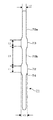
続いて本発明の要部が構成されているステージ(載置台)41の周辺の載置機構の構成について図2〜図3をも参照しながら説明する。ステージ41は例えば円形に構成され、処理容器20の小径の円筒部20bの底部に支持部材42を介して支持されて、処理容器20の大径の円筒部20aの中央部に位置するように設けられており、このステージ41の載置面41aに載置されたウエハWは水平に保たれるようになっている。図中43はステージ41に埋めこまれた、ステージ41上のウエハWの温調手段をなすヒータであり、図中44は載置面41a上のウエハWを吸着する静電チャックである。このステージ41は接地されており、ウエハWを載置する載置台の役割の他に下部電極としての役割を有している。なお図1では配線図は略解的に記載してあるが実際にはステージ41は処理容器20に電気的に接続されている。
Next, the configuration of the mounting mechanism around the stage (mounting table) 41 on which the main part of the present invention is configured will be described with reference to FIGS. The
ステージ41の例えば周方向には夫々間隔をおいて3つの貫通孔40が鉛直方向に形成されており、この貫通孔40内には例えばアルミナ等の材質により構成された円筒状のスリーブ51が設けられている。なお図中52はこのスリーブ51の孔であるピン挿通孔であり、図中53はスリーブ51の下端側の開口部である。スリーブ51の上端にはフランジ部51aが形成されており、このフランジ部51aが前記貫通孔40の上部側の拡径領域(凹部)に嵌入されることにより、スリーブ51がステージ41内に埋め込まれ、フランジ部51aの上面がステージ41の載置面41aと略同じ高さに位置している。
In the circumferential direction of the
スリーブ51の下部の外周にはねじが切られ、2つのナット54、54をスリーブ51に螺合させてステージ41の下面側に締め付けることによって、スリーブ51がステージ41に固着されている。このスリーブ51の長さはこの例ではステージ41の厚さよりも大きく形成され、スリーブ51の下端はステージ41の下方へと突出している。スリーブ51をこのような構成とすることでステージ41の下方に回りこんだ処理ガスが開口部53からピン挿通孔52内に侵入した場合その進入した処理ガスがピン挿通孔52内の上部側に達することが抑えられるため、このピン挿通孔52の上部側及び後述するリフタピン61の先端側に処理ガスによるデポ物が付着しにくくなる。
The outer periphery of the lower portion of the
スリーブ51の下端側の開口部53においては内側に向かうように環状に突出して形成された環状突出部56が設けられている。この環状突出部56の上側の面はリフタピン61が下降した場合に当該リフタピン61に当接してこれを支持する支持面57をなし、内側下方に向かって傾斜するように形成されている。
The
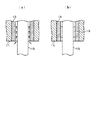
続いてリフタピン61について説明する。図3に示すようにリフタピン61は各スリーブ51の上部側からスリーブ51のピン挿通孔52内に挿入され、後述するように当該ピン挿通孔52内を昇降できるようになっている。このリフタピン61は例えばアルミナなどの材質により構成される。リフタピン61の中央には拡径部62が設けられており、この拡径部62における下端部即ち拡径部62から小径部分に移行する段差面63は例えば下方に向かうに従って徐々に縮径しており、言い換えれば内側下方に向かって傾斜している。この傾斜した段差面63はリフタピン61からピンベース64が離れているときに、支持面57に面接触し、これによりスリーブ51の下端側の開口部53が塞がれてこの開口部53からスリーブ51のピン挿通孔52内への気体の流入が抑えられるようになっている。なお以下の説明ではこのときのリフタピン61の位置をホームポジション(下降位置)と呼ぶ。
Next, the
またこのリフタピン61における拡径部62よりも上方側部分は、拡径部62よりも小径な小径部60として形成されている。拡径部62の軸方向の長さについては、リフタピン61がステージ41の載置面41aよりも突出してウエハWに対する受け渡し位置にあるときには、載置面41aよりも突出しないような寸法に設定されている。これはリフタピン61の拡径部62がスリーブ51の内壁をこすり、内壁に付着した成膜ガスによるデポ物を載置面41a上に押し上げ、このデポ物がパーティクルとして載置面41aに載置されたウエハWに付着することを防ぐためである。
Further, the upper portion of the
また拡径部62の外周面とスリーブ51の内周面との隙間は、リフタピン61がスムーズに昇降できる大きさであることが必要であるが、あまり大きいとリフタピン61の昇降動作が不安定になって次に述べるようにリフタピン61の傾きが大きくなって小径部60がスリーブ51の内周面に接触してしまうし、更にまた成膜ガスが下方から侵入したときに上側まで容易に入り込んでしまうことから、これらの兼ね合いで決定される。
Further, the clearance between the outer peripheral surface of the
拡径部62は、このように成膜ガスの上方側への侵入を抑える役割を果たすだけでなく、この例では、拡径部62とスリーブ51との隙間が小さいのでリフタピン61が傾いたときに、拡径部62自身がスリーブ51の内周面に接触してその傾きを抑え、これによりその上方の小径部60がスリーブ51の内周面に接触しないようにする役割も持っている。即ち、拡径部62とスリーブ51との隙間が小さいのでリフタピン61が傾いたときに、リフタピン61とスリーブ51との接触点が拡径部62の外周面となり、その上の小径部60は接触しないようになっている。従って小径部60がスリーブ51の内壁を擦ってデポ物(付着物)を載置面上41aに押し上げるおそれがない。
In this example, the
ここで各部位の寸法の一例を挙げておくと、図4に示すようにスリーブ51の口径dは4mm、拡径部62の長さL及び外径R1は、夫々20mm及び3.6mm、小径部60の外径r1は、2mmである。
Here, as an example of the dimensions of each part, as shown in FIG. 4, the diameter d of the
ホームポジションにあるリフタピンの下方側には例えばリフタピン61と間隔をおいてリフタピン61を押し上げるためのピンベース64が設けられており、各ピンベース64の下部にはこららピンベース64を支持するリフタアーム65が接続されている。この例ではピンベース64およびリフタアーム65により昇降体が構成される。図中66は駆動ロッドであり、その一端は前記リフタアーム65に接続されており、その他端は例えば円筒部20aの底面にて図示しない軸受け部を介して処理容器20の外へ伸長して昇降機構67に接続されている。図中68は駆動ロッド66と処理容器20との気密性を確保するためのベローズである。昇降機構67は駆動ロッド66を介してリフタアーム65を上昇させ、このリフタアーム65の上昇によりピンベース64が鉛直方向に上昇する。上昇したピンベース64はホームポジションに位置するリフタピン61の下端に当接し、さらにリフタピン61を鉛直方向に押し上げることでリフタピン61は上昇してその先端部が載置面41a上に突出するようになっている。
On the lower side of the lifter pin at the home position, for example, a
続いてこの成膜装置2により行われる一連の動作について説明する。先ずゲートバルブ23が開き、被処理基板であるウエハWが図示しない搬送機構により搬送口24を介して処理容器20内に搬入される。ウエハWがステージ41の中央部上に搬送されると昇降機構67により駆動ロッド66及びリフタアーム65を介してピンベース64が上昇する。図5(a)はホームポジションに位置するリフタピン61を示しており、ピンベース64が上昇するとリフタピン61下端に当接し、リフタピン61は鉛直方向に押し上げられて載置面41a上に突出する。図5(b)に示すようにリフタピン61の先端がウエハWの裏面を支持するとピンベース64の上昇が停止することによって、リフタピン61の上昇も停止する。上方向への付勢を失ったリフタピン61は傾き、同図に示すようにスリーブ51の内壁に拡径部62の上端が接する。なおリフタピン61と搬送機構とは平面的に干渉しないようになっている。
Next, a series of operations performed by the
その後、ピンベース64が下降するとリフタピン61がウエハWを保持した状態で下降し、スリーブ51内に没入すると、ウエハWが載置面41a上に載置される。さらにピンベース64の下降に伴いリフタピン61が下降すると拡径部62の下端の段差面63がスリーブの環状突起部56の支持面57に当接し、リフタピン61の自重により拡径部62側の段差面63が、支持面57に案内されながら滑り落ちて支持面57で囲まれるいわばすり鉢部に嵌合されて支持され、リフタピン61の軸P1とスリーブ51の軸Q1とが一致した状態(リフタピン61上昇前の図5(a)参照)つまりリフタピン61がスリーブ51の中心に位置合わせされた状態でリフタピン61がスリーブ51の環状突出部56に支持されることになる。このときピンベース64はリフタピン61よりも下方に位置する。
Thereafter, when the
一方、搬送機構が処理容器20内から退避し、ゲートバルブが閉じられると次にガス吐出口33A、33Bから処理空間26に処理ガスが吐出される。このようなガス供給が行われる一方で真空ポンプ22により処理容器20内が真空排気されて所定の圧力に設定され、またヒータ43及び処理容器20の内壁が夫々設定温度に加熱される。続いて高周波電源部32から上部電極であるガスシャワーヘッド3と下部電極であるステージ41との間に高周波電力を供給することによって、TiCl4ガス及びNH3ガスがプラズマ化されてウエハW上にTiNが堆積されて薄膜が形成される。
On the other hand, when the transfer mechanism is retracted from the
所定時間プロセスが行われると、高周波電力の供給及び各ガスの供給が停止され、その後リフタピン61及び搬送機構による搬送動作が既述の搬入動作と逆の手順で行われてウエハWが処理容器20内から搬出される。
When the process is performed for a predetermined time, the supply of high-frequency power and the supply of each gas are stopped, and then the transfer operation by the lifter pins 61 and the transfer mechanism is performed in the reverse order of the transfer operation described above, and the wafer W is processed into the
本実施形態のウエハWの載置機構2は、ステージ41に形成された貫通孔に設けられたスリーブ51の下端の開口部53に環状突出部56を形成し、リフタピン61が下降したときにこれに形成された拡径部62が環状突出部56に支持されて前記開口部53を塞ぐようにしている。従ってウエハWが載置されたステージ41の下方側に回り込んだ処理ガスは、スリーブ51の下端から侵入しにくくなり、処理ガスから生成したデポ物がリフタピン61とスリーブ51との間の隙間に蓄積することが抑えられる。従ってリフタピン61の昇降が阻害されることが抑えられ、その結果としてリフタピン61の正常な動作を確保するための、リフタピン61及びスリーブ51のクリーニングや交換等のメンテナンス作業を行う頻度を減らすことができる。
The wafer
またリフタピン61がホームポジションに戻るときには拡径部62が環状突出部56の傾斜面に案内されることでリフタピン61の姿勢が垂直状態に規制され、リフタピン61とスリーブ51との各中心軸が一致した状態になる。この例では、ホームポジションにあるリフタピン61を傾けたときに拡径部62とスリーブ51との接触により小径部がスリーブ51に接触しないようになっているので、リフタピン61の上昇時にはその上部側の小径部60がスリーブ51に接触することはないが、このような寸法設定をしなくてもリフタピン61は垂直姿勢で押し上げられ、しかも拡径部62よりも上部側は小径部となっているので、上昇する際にリフタピン61の上部側がスリーブ51に接触しなくなり、加えて拡径部62についてもスリーブ51の内壁と接触しにくくなる。従ってスリーブ51の内壁に付着したデポ物がこのリフタピン61により剥離されて押し上げられ、載置面41aに乗ることが抑えられる。その結果としてこのデポ物がパーティクルとなりウエハWを汚染することが抑えられる。
Further, when the
なお既述の実施形態においてはリフタピン61とピンベース64とは離れているが、リフタピン61がホームポジションに位置する際に前記開口部53を塞ぐことができれば本発明の効果が得られるため、例えばリフタピン61とピンベース64とが接続されるとともに、ピンベース64によりリフタピン61が垂直に支持されているような構成も本発明の権利範囲に含まれる。
In the above-described embodiment, the
またリフタピンは既述の実施形態のような形状とすることに限られず図6に示すような形状としてもよい。この図6に示すリフタピン71はその中央部に間隔をおいて第1の拡径部72、第2の拡径部73が先端側に向かってこの順に設けられている。このリフタピン71において第2の拡径部73の上側、及び第1の拡径部72と第2の拡径部73との間は、夫々各拡径部よりも小径な小径部70a,70bとして形成されている。第1の拡径部72の下端には既述のリフタピン61の拡径部62の下端と同様に傾斜した段差面74が形成され、図6(a)に示すようにリフタピン71がホームポジションに位置するときはスリーブ51の環状突出部56にこの段差面74が支持されて、既述の例と同様にリフタピン71が垂直姿勢でスリーブ51の開口部53を塞ぐようになっている。
Further, the lifter pin is not limited to the shape as in the above-described embodiment, and may have a shape as shown in FIG. The
そして図6(b)に示すように、リフタピン71がホームポジションにあるときに傾いたとしても第2の拡径部73がスリーブ51の内壁に接触することで、それよりも上の小径部70aがスリーブ51の内壁に接触しないように各寸法が設定されている。また図6(c)に示すようにリフタピン71がピンベース64により持ち上げられ、リフタピン71の先端部が載置面41a上に突出した際には第2の拡径部73はスリーブ51内に留まるように構成されている。
As shown in FIG. 6B, even if the
このリフタピン71の各部の大きさの一例を示すと、図7にl1で示す第1の拡径部72の長さは6mmであり、l2で示す第2の拡径部73の長さは6mmである。またl3で示す拡径部72と拡径部73とにより挟まれる小径部70bの長さは7.4mmである。前記小径部70a、70bの径の大きさr2は2mmであり、各拡径部の径の大きさR2は3.6mmである。なおスリーブ51の内径は先の例と同じである。
An example of the size of each part of the
通常デポ物を生成するガスが固体と固体との隙間に入り込むとそのガスのデポ物はその隙間のある部位に集中的に付着する傾向があるが、このようにリフタピン71を構成した場合、このリフタピン71がホームポジションに位置するときに開口部53からピン挿通孔52内へ前記TiCl4等の処理ガスが漏れて流入しても、その処理ガスは拡径部72とスリーブ51との隙間から拡径部72と拡径部73との間の広いスペースに拡散される。その結果として前記処理ガスから生成したデポ物が、拡径部72とスリーブ51との隙間に集中的に付着して、リフタピン71の昇降が阻害されることを抑えることができるためリフタピン71及びスリーブ51の交換頻度が短くなることを抑えることができる。
Normally, when a gas that generates a depot enters the gap between the solids, the depot of the gas tends to concentrate on the portion having the gap. However, when the
さらに図8に示すようにステージ(載置台)41に形成された貫通孔40に、直接リフタピンを挿入した構成であってもよい。具体的には、ステージ41の貫通孔40の下端側の開口部80に、内側に向かうように環状に突出して形成された環状突出部81が設けられている。この環状突出部81の上側の面は後述するリフタピン8が下降したときに当該リフタピン8に当接してこれを支持する支持面82をなし、内側方向に向かって傾斜するように形成されている。
Furthermore, as shown in FIG. 8, the structure which inserted the lifter pin directly in the through-
この貫通孔40内に挿入されるリフタピン8は、図8に示すように図6に示した実施例と同様の拡径部8aが中央部分に1個設けられている。即ち、この拡径部8aの上側は当該各径部8aよりも小径な小径部8bとして形成されている。また拡径部8aの下端には既述のリフタピン61の拡径部61の下端と同様に傾斜した段差面83が形成され、図8(a)に示すようにリフタピン8がホームポジションに位置するときにはステージ41の環状突出部81にこの段差面83が支持されて、既述の例と同様にリフタピン8が垂直姿勢でステージ41の開口部80を塞ぐようになっている。
As shown in FIG. 8, the
また図8(b)に示すように、リフタピン8がピンベース64により持ち上げられ、リフタピン8の先端部が載置面41a上に突出した際には前記拡径部8aはステージ41内に留まるように構成されている。
Further, as shown in FIG. 8B, when the
上述の例では、ステージ41の貫通孔40内に直接リフタピン8を挿入しているので、既述のようにスリーブ51を設けた場合に比べて、リフタピンを挿入する孔の全長が短くなる。そのため成膜装置2内にクリーニングガスを供給し、当該成膜装置2内をクリーニングする処理において、クリーニングガスがステージ41の貫通孔40の下方側まで到達し易くなり、貫通孔40の下方側に付着したデポ物(堆積物)を取り除き易くなる利点がある。
In the above example, since the lifter pins 8 are directly inserted into the through
また載置機構を構成する部品点数が少ないことから、部品を組み付ける作業時間を短縮することができ、コストの低減化も図れる。 In addition, since the number of parts constituting the mounting mechanism is small, it is possible to shorten the work time for assembling the parts and to reduce the cost.
2 成膜装置
41 ステージ
41a 載置面
51 スリーブ
52 ピン挿通孔
53 開口部
56 環状突出部
61 リフタピン
62 拡径部
64 ピンベース
DESCRIPTION OF
Claims (9)
前記ピン挿通孔の下端の開口部に内側に環状に突出して形成された環状突出部と、
前記リフタピンに形成され、当該リフタピンが下降したときに環状突出部に支持されて前記開口部を塞ぐ第1の拡径部と、
この第1の拡径部よりも上方側であってかつリフタピンが基板を受け取る上昇位置にあるときにリフタピンにおけるピン挿通孔の中に位置する部分に設けられた第2の拡径部と、を備えたことを特徴とする基板載置機構。 Provided in a processing container that forms a processing atmosphere by a processing gas, and is inserted into a mounting table on which a substrate to be processed is mounted and a pin insertion hole provided in the mounting table, and the substrate is transferred to the mounting table by a retracting operation. In a substrate mounting mechanism comprising a plurality of lifter pins for carrying out and lifting and lowering bodies that support these lifter pins, and lifting and lowering the lifter pins through the lifting body by the lifting mechanism,
An annular protrusion formed annularly inwardly in the opening at the lower end of the pin insertion hole;
A first diameter-increased portion formed on the lifter pin and supported by an annular protrusion when the lifter pin is lowered to close the opening;
A second enlarged-diameter portion provided in a portion located in the pin insertion hole in the lifter pin when the lifter pin is in the raised position for receiving the substrate above the first enlarged-diameter portion; A substrate mounting mechanism comprising the substrate mounting mechanism.
前記ピン挿通孔の下端の開口部に内側に環状に突出して形成された環状突出部と、
前記リフタピンに形成され、当該リフタピンが下降したときに環状突出部に支持されて前記開口部を塞ぎ、前記スリーブの内径よりも上下方向の長さ寸法が大きい拡径部と、を備え、
前記拡径部の下面側は、内側下方に向かって傾斜し、また前記環状突出部の上面側は、拡径部を案内してリフタピンをピン挿通孔の中央に位置させるために内側下方に向かって傾斜し、
前記リフタピンにおいて、基板を支持するときに突出する部分は拡径部よりも小径に形成され、
前記リフタピンは昇降体とは分離されて設けられており、リフタピンの自重により拡径部が環状突出部に支持され、
前記スリーブ内でリフタピンを傾けたときに拡径部とスリーブとが接触することで、リフタピンの小径部がスリーブに接触しないようにするために、前記拡径部の長さ寸法が設定されていることを特徴とする基板載置機構。 A mounting table provided for mounting a substrate to be processed in a processing container forming a processing atmosphere by a processing gas, and having a through hole, a pin insertion hole, and the mounting table from within the through hole of the mounting table A sleeve provided so as to protrude downward, a lifter pin inserted into the pin insertion hole for transferring the substrate to the mounting table by a retracting operation, a lifting body for supporting the lifter pin, and the lifting body In the substrate mounting mechanism comprising a lifting mechanism that lifts and lowers the lifter pin through,
An annular protrusion formed annularly inwardly in the opening at the lower end of the pin insertion hole;
The lifter pins are formed on, busy technique the opening the lifter pins is supported on the annular projection when lowered, and a diameter-increased portion length dimension in the vertical direction is greater than the inner diameter of the sleeve,
The lower surface side of the enlarged diameter portion is inclined inward and downward, and the upper surface side of the annular projecting portion is directed inward and downward to guide the enlarged diameter portion and position the lifter pin at the center of the pin insertion hole. Tilt and
In the lifter pin, the portion protruding when supporting the substrate is formed to have a smaller diameter than the enlarged diameter portion,
The lifter pin is provided separately from the lifting body, the enlarged diameter portion is supported by the annular protrusion by the weight of the lifter pin,
When the lifter pin is tilted in the sleeve, the enlarged diameter portion and the sleeve come into contact with each other so that the small diameter portion of the lifter pin does not contact the sleeve, and the length of the enlarged diameter portion is set. A substrate mounting mechanism characterized by that.
前記スリーブの下部の外周にはねじが切られ、ナットをスリーブに螺合させて載置台の下面側に締め付けることによって、スリーブが載置台に固着され、スリーブの下端はナットの下方へ突出していることを特徴とする請求項1ないし7のいずれか一項に記載の基板載置機構。 A screw is cut on the outer periphery of the lower portion of the sleeve, and the sleeve is fixed to the mounting table by screwing the nut into the sleeve and tightening to the lower surface side of the mounting table, and the lower end of the sleeve protrudes below the nut. The substrate mounting mechanism according to any one of claims 1 to 7, wherein
Priority Applications (5)
| Application Number | Priority Date | Filing Date | Title |
|---|---|---|---|
| JP2006095167A JP4687534B2 (en) | 2005-09-30 | 2006-03-30 | Substrate mounting mechanism and substrate processing apparatus |
| US11/527,730 US20070089672A1 (en) | 2005-09-30 | 2006-09-27 | Substrate placing mechanism |
| KR1020060094970A KR100951148B1 (en) | 2005-09-30 | 2006-09-28 | Substrate loading mechanism and substrate processing apparatus |
| TW095136443A TW200717695A (en) | 2005-09-30 | 2006-09-29 | Substrate loading mechanism and substrate processing apparatus |
| KR1020080064930A KR100909499B1 (en) | 2005-09-30 | 2008-07-04 | Substrate loading mechanism and substrate processing apparatus |
Applications Claiming Priority (3)
| Application Number | Priority Date | Filing Date | Title |
|---|---|---|---|
| JP2005288295 | 2005-09-30 | ||
| JP2005288295 | 2005-09-30 | ||
| JP2006095167A JP4687534B2 (en) | 2005-09-30 | 2006-03-30 | Substrate mounting mechanism and substrate processing apparatus |
Publications (3)
| Publication Number | Publication Date |
|---|---|
| JP2007123810A JP2007123810A (en) | 2007-05-17 |
| JP2007123810A5 JP2007123810A5 (en) | 2009-02-26 |
| JP4687534B2 true JP4687534B2 (en) | 2011-05-25 |
Family
ID=37984168
Family Applications (1)
| Application Number | Title | Priority Date | Filing Date |
|---|---|---|---|
| JP2006095167A Expired - Fee Related JP4687534B2 (en) | 2005-09-30 | 2006-03-30 | Substrate mounting mechanism and substrate processing apparatus |
Country Status (4)
| Country | Link |
|---|---|
| US (1) | US20070089672A1 (en) |
| JP (1) | JP4687534B2 (en) |
| KR (2) | KR100951148B1 (en) |
| TW (1) | TW200717695A (en) |
Cited By (1)
| Publication number | Priority date | Publication date | Assignee | Title |
|---|---|---|---|---|
| KR20210023427A (en) * | 2019-08-23 | 2021-03-04 | 세메스 주식회사 | Assembly for supporting substrate and apparatus for processing having the same |
Families Citing this family (30)
| Publication number | Priority date | Publication date | Assignee | Title |
|---|---|---|---|---|
| TWI349720B (en) * | 2007-05-30 | 2011-10-01 | Ind Tech Res Inst | A power-delivery mechanism and apparatus of plasma-enhanced chemical vapor deposition using the same |
| JP5148955B2 (en) | 2007-09-11 | 2013-02-20 | 東京エレクトロン株式会社 | Substrate mounting mechanism and substrate processing apparatus |
| US20090314211A1 (en) * | 2008-06-24 | 2009-12-24 | Applied Materials, Inc. | Big foot lift pin |
| US8218284B2 (en) * | 2008-07-24 | 2012-07-10 | Hermes-Microvision, Inc. | Apparatus for increasing electric conductivity to a semiconductor wafer substrate when exposure to electron beam |
| JP5155790B2 (en) * | 2008-09-16 | 2013-03-06 | 東京エレクトロン株式会社 | Substrate mounting table and substrate processing apparatus using the same |
| US8094428B2 (en) * | 2008-10-27 | 2012-01-10 | Hermes-Microvision, Inc. | Wafer grounding methodology |
| US9011602B2 (en) * | 2009-01-29 | 2015-04-21 | Lam Research Corporation | Pin lifting system |
| CN101812676B (en) * | 2010-05-05 | 2012-07-25 | 江苏综艺光伏有限公司 | Processing chamber used for semiconductor solar film plating |
| US9728429B2 (en) | 2010-07-27 | 2017-08-08 | Lam Research Corporation | Parasitic plasma prevention in plasma processing chambers |
| KR101432916B1 (en) * | 2013-01-04 | 2014-08-21 | 주식회사 엘지실트론 | Wafer lift apparatus |
| US9991153B2 (en) * | 2013-03-14 | 2018-06-05 | Applied Materials, Inc. | Substrate support bushing |
| US10195704B2 (en) * | 2013-03-15 | 2019-02-05 | Infineon Technologies Ag | Lift pin for substrate processing |
| US10192770B2 (en) * | 2014-10-03 | 2019-01-29 | Applied Materials, Inc. | Spring-loaded pins for susceptor assembly and processing methods using same |
| JP6403100B2 (en) * | 2016-01-25 | 2018-10-10 | 信越半導体株式会社 | Epitaxial growth apparatus and holding member |
| KR102339350B1 (en) * | 2017-04-03 | 2021-12-16 | 주식회사 미코세라믹스 | Ceramic heater |
| WO2019004201A1 (en) * | 2017-06-26 | 2019-01-03 | エピクルー ユーエスエー インコーポレイテッド | Processing chamber |
| JP6386632B2 (en) * | 2017-07-06 | 2018-09-05 | 東京エレクトロン株式会社 | Plasma processing equipment |
| KR101999449B1 (en) | 2017-11-23 | 2019-07-11 | 지현숙 | Water purifier for domestic nano bubble generation |
| JP6994981B2 (en) * | 2018-02-26 | 2022-01-14 | 東京エレクトロン株式会社 | Manufacturing method of plasma processing equipment and mounting table |
| KR20190102812A (en) | 2018-02-27 | 2019-09-04 | 지현숙 | Water purifier for domestic nano bubble generation |
| KR20190105420A (en) | 2018-03-05 | 2019-09-17 | 지현숙 | Water purifier for domestic nano bubble generation |
| JP7214021B2 (en) * | 2018-03-29 | 2023-01-27 | 東京エレクトロン株式会社 | PLASMA PROCESSING APPARATUS AND OBJECT CONVEYING METHOD |
| JP7018801B2 (en) * | 2018-03-29 | 2022-02-14 | 東京エレクトロン株式会社 | Plasma processing equipment and method of transporting the object to be processed |
| JP2021012952A (en) * | 2019-07-05 | 2021-02-04 | 東京エレクトロン株式会社 | Mounting stage, substrate processing apparatus, and assembly method of mounting stage |
| KR20220042114A (en) | 2019-07-25 | 2022-04-04 | 에피크루 가부시키가이샤 | Process chamber of epitaxial growth apparatus |
| JP2021097162A (en) * | 2019-12-18 | 2021-06-24 | 東京エレクトロン株式会社 | Substrate processing device and mounting table |
| CN113035682B (en) * | 2019-12-25 | 2023-03-31 | 中微半导体设备(上海)股份有限公司 | Lower electrode assembly and plasma processing device thereof |
| KR102588603B1 (en) * | 2020-09-23 | 2023-10-13 | 세메스 주식회사 | lift pin assembly and Apparatus for treating substrate with the assembly |
| USD980884S1 (en) | 2021-03-02 | 2023-03-14 | Applied Materials, Inc. | Lift pin |
| CN115341198B (en) * | 2022-07-05 | 2023-08-04 | 湖南红太阳光电科技有限公司 | Flat plate type PECVD equipment |
Citations (5)
| Publication number | Priority date | Publication date | Assignee | Title |
|---|---|---|---|---|
| JPS631044A (en) * | 1986-06-20 | 1988-01-06 | Hitachi Electronics Eng Co Ltd | Vapor phase reaction equipment |
| JP2002231794A (en) * | 2001-02-02 | 2002-08-16 | Tokyo Electron Ltd | Mechanism of placing workpiece |
| JP2003197719A (en) * | 2001-12-21 | 2003-07-11 | Komatsu Electronic Metals Co Ltd | Device for manufacturing semiconductor and structure for supporting substrate |
| JP2004214312A (en) * | 2002-12-27 | 2004-07-29 | Ulvac Japan Ltd | Substrate processing apparatus |
| JP2004349516A (en) * | 2003-05-23 | 2004-12-09 | Hitachi High-Technologies Corp | Substrate processor |
Family Cites Families (6)
| Publication number | Priority date | Publication date | Assignee | Title |
|---|---|---|---|---|
| JPH10132104A (en) * | 1996-10-28 | 1998-05-22 | Smc Corp | Pilot type three port directional control valve |
| JP3602324B2 (en) * | 1998-02-17 | 2004-12-15 | アルプス電気株式会社 | Plasma processing equipment |
| US6958098B2 (en) * | 2000-02-28 | 2005-10-25 | Applied Materials, Inc. | Semiconductor wafer support lift-pin assembly |
| KR100421783B1 (en) * | 2000-12-14 | 2004-03-10 | 볼보 컨스트럭션 이키프먼트 홀딩 스웨덴 에이비 | pressure control valve of pilot poppet |
| US6887317B2 (en) * | 2002-09-10 | 2005-05-03 | Applied Materials, Inc. | Reduced friction lift pin |
| KR100520817B1 (en) * | 2003-11-14 | 2005-10-12 | 삼성전자주식회사 | Apparatus for supporting a semiconductor substrate and apparatus for manufacturing a semiconductor device having the same |
-
2006
- 2006-03-30 JP JP2006095167A patent/JP4687534B2/en not_active Expired - Fee Related
- 2006-09-27 US US11/527,730 patent/US20070089672A1/en not_active Abandoned
- 2006-09-28 KR KR1020060094970A patent/KR100951148B1/en not_active IP Right Cessation
- 2006-09-29 TW TW095136443A patent/TW200717695A/en unknown
-
2008
- 2008-07-04 KR KR1020080064930A patent/KR100909499B1/en active IP Right Grant
Patent Citations (5)
| Publication number | Priority date | Publication date | Assignee | Title |
|---|---|---|---|---|
| JPS631044A (en) * | 1986-06-20 | 1988-01-06 | Hitachi Electronics Eng Co Ltd | Vapor phase reaction equipment |
| JP2002231794A (en) * | 2001-02-02 | 2002-08-16 | Tokyo Electron Ltd | Mechanism of placing workpiece |
| JP2003197719A (en) * | 2001-12-21 | 2003-07-11 | Komatsu Electronic Metals Co Ltd | Device for manufacturing semiconductor and structure for supporting substrate |
| JP2004214312A (en) * | 2002-12-27 | 2004-07-29 | Ulvac Japan Ltd | Substrate processing apparatus |
| JP2004349516A (en) * | 2003-05-23 | 2004-12-09 | Hitachi High-Technologies Corp | Substrate processor |
Cited By (2)
| Publication number | Priority date | Publication date | Assignee | Title |
|---|---|---|---|---|
| KR20210023427A (en) * | 2019-08-23 | 2021-03-04 | 세메스 주식회사 | Assembly for supporting substrate and apparatus for processing having the same |
| KR102297311B1 (en) * | 2019-08-23 | 2021-09-02 | 세메스 주식회사 | Assembly for supporting substrate and apparatus for processing having the same |
Also Published As
| Publication number | Publication date |
|---|---|
| US20070089672A1 (en) | 2007-04-26 |
| JP2007123810A (en) | 2007-05-17 |
| TW200717695A (en) | 2007-05-01 |
| KR100951148B1 (en) | 2010-04-07 |
| KR20070037363A (en) | 2007-04-04 |
| KR20080077941A (en) | 2008-08-26 |
| KR100909499B1 (en) | 2009-07-27 |
Similar Documents
| Publication | Publication Date | Title |
|---|---|---|
| JP4687534B2 (en) | Substrate mounting mechanism and substrate processing apparatus | |
| CN111430232B (en) | Plasma processing apparatus and mounting table for plasma processing apparatus | |
| JP3398936B2 (en) | Semiconductor processing equipment | |
| KR102077438B1 (en) | Semiconductor manufacturing device and processing method | |
| JP4354243B2 (en) | Elevating mechanism and processing apparatus for workpiece | |
| JP5091906B2 (en) | Elevating mechanism and processing apparatus for workpiece | |
| JP2007189222A (en) | Semiconductor processing apparatus with lift pin structure | |
| US11512391B2 (en) | Process kit for a high throughput processing chamber | |
| JP2006196691A (en) | Device for manufacturing semiconductor and manufacturing method for semiconductor device | |
| CN100440476C (en) | Substrate placing mechanism and substrate processing device | |
| KR20070098674A (en) | Substrate transferring apparatus, substrate processing apparatus, and substrate processing method | |
| CN112992769A (en) | Substrate processing apparatus and mounting table | |
| CN104733367B (en) | Lift pin assembly and substrate processing apparatus having the same | |
| JP4367959B2 (en) | Plasma processing equipment | |
| JP4450983B2 (en) | Plasma processing equipment for liquid crystal display substrate | |
| TWI834491B (en) | Plasma processing appratus and ring assembly thereof | |
| KR20220005993A (en) | Plasma processing apparatus and substrate support of plasma processing apparatus | |
| JP2023062845A (en) | Conveying method of object to be processed and processing apparatus | |
| CN113948438A (en) | Electrostatic chuck, etching semiconductor equipment and wafer mounting method | |
| KR20050112731A (en) | Lift pin assemable of semiconductor production device | |
| KR20070080766A (en) | Apparatus and method for treating a substrate | |
| WO2016178754A1 (en) | Process kit for a high throughput processing chamber |
Legal Events
| Date | Code | Title | Description |
|---|---|---|---|
| A521 | Request for written amendment filed |
Free format text: JAPANESE INTERMEDIATE CODE: A523 Effective date: 20090108 |
|
| A621 | Written request for application examination |
Free format text: JAPANESE INTERMEDIATE CODE: A621 Effective date: 20090108 |
|
| A977 | Report on retrieval |
Free format text: JAPANESE INTERMEDIATE CODE: A971007 Effective date: 20100924 |
|
| A131 | Notification of reasons for refusal |
Free format text: JAPANESE INTERMEDIATE CODE: A131 Effective date: 20101005 |
|
| A521 | Request for written amendment filed |
Free format text: JAPANESE INTERMEDIATE CODE: A523 Effective date: 20101206 |
|
| TRDD | Decision of grant or rejection written | ||
| A01 | Written decision to grant a patent or to grant a registration (utility model) |
Free format text: JAPANESE INTERMEDIATE CODE: A01 Effective date: 20110118 |
|
| A01 | Written decision to grant a patent or to grant a registration (utility model) |
Free format text: JAPANESE INTERMEDIATE CODE: A01 |
|
| A61 | First payment of annual fees (during grant procedure) |
Free format text: JAPANESE INTERMEDIATE CODE: A61 Effective date: 20110131 |
|
| R150 | Certificate of patent or registration of utility model |
Free format text: JAPANESE INTERMEDIATE CODE: R150 |
|
| FPAY | Renewal fee payment (event date is renewal date of database) |
Free format text: PAYMENT UNTIL: 20140225 Year of fee payment: 3 |
|
| R250 | Receipt of annual fees |
Free format text: JAPANESE INTERMEDIATE CODE: R250 |
|
| LAPS | Cancellation because of no payment of annual fees |