JP4681184B2 - 広帯域な励起を有する発光ダイオード白色光源 - Google Patents
広帯域な励起を有する発光ダイオード白色光源 Download PDFInfo
- Publication number
- JP4681184B2 JP4681184B2 JP2001535238A JP2001535238A JP4681184B2 JP 4681184 B2 JP4681184 B2 JP 4681184B2 JP 2001535238 A JP2001535238 A JP 2001535238A JP 2001535238 A JP2001535238 A JP 2001535238A JP 4681184 B2 JP4681184 B2 JP 4681184B2
- Authority
- JP
- Japan
- Prior art keywords
- light emitting
- light source
- white light
- emitting diode
- source according
- Prior art date
- Legal status (The legal status is an assumption and is not a legal conclusion. Google has not performed a legal analysis and makes no representation as to the accuracy of the status listed.)
- Expired - Lifetime
Links
Images


Classifications
-
- H—ELECTRICITY
- H01—ELECTRIC ELEMENTS
- H01L—SEMICONDUCTOR DEVICES NOT COVERED BY CLASS H10
- H01L33/00—Semiconductor devices with at least one potential-jump barrier or surface barrier specially adapted for light emission; Processes or apparatus specially adapted for the manufacture or treatment thereof or of parts thereof; Details thereof
- H01L33/48—Semiconductor devices with at least one potential-jump barrier or surface barrier specially adapted for light emission; Processes or apparatus specially adapted for the manufacture or treatment thereof or of parts thereof; Details thereof characterised by the semiconductor body packages
- H01L33/50—Wavelength conversion elements
-
- H—ELECTRICITY
- H01—ELECTRIC ELEMENTS
- H01L—SEMICONDUCTOR DEVICES NOT COVERED BY CLASS H10
- H01L33/00—Semiconductor devices with at least one potential-jump barrier or surface barrier specially adapted for light emission; Processes or apparatus specially adapted for the manufacture or treatment thereof or of parts thereof; Details thereof
- H01L33/02—Semiconductor devices with at least one potential-jump barrier or surface barrier specially adapted for light emission; Processes or apparatus specially adapted for the manufacture or treatment thereof or of parts thereof; Details thereof characterised by the semiconductor bodies
- H01L33/08—Semiconductor devices with at least one potential-jump barrier or surface barrier specially adapted for light emission; Processes or apparatus specially adapted for the manufacture or treatment thereof or of parts thereof; Details thereof characterised by the semiconductor bodies with a plurality of light emitting regions, e.g. laterally discontinuous light emitting layer or photoluminescent region integrated within the semiconductor body
-
- H—ELECTRICITY
- H01—ELECTRIC ELEMENTS
- H01L—SEMICONDUCTOR DEVICES NOT COVERED BY CLASS H10
- H01L2224/00—Indexing scheme for arrangements for connecting or disconnecting semiconductor or solid-state bodies and methods related thereto as covered by H01L24/00
- H01L2224/01—Means for bonding being attached to, or being formed on, the surface to be connected, e.g. chip-to-package, die-attach, "first-level" interconnects; Manufacturing methods related thereto
- H01L2224/26—Layer connectors, e.g. plate connectors, solder or adhesive layers; Manufacturing methods related thereto
- H01L2224/31—Structure, shape, material or disposition of the layer connectors after the connecting process
- H01L2224/32—Structure, shape, material or disposition of the layer connectors after the connecting process of an individual layer connector
- H01L2224/321—Disposition
- H01L2224/32151—Disposition the layer connector connecting between a semiconductor or solid-state body and an item not being a semiconductor or solid-state body, e.g. chip-to-substrate, chip-to-passive
- H01L2224/32221—Disposition the layer connector connecting between a semiconductor or solid-state body and an item not being a semiconductor or solid-state body, e.g. chip-to-substrate, chip-to-passive the body and the item being stacked
- H01L2224/32245—Disposition the layer connector connecting between a semiconductor or solid-state body and an item not being a semiconductor or solid-state body, e.g. chip-to-substrate, chip-to-passive the body and the item being stacked the item being metallic
-
- H—ELECTRICITY
- H01—ELECTRIC ELEMENTS
- H01L—SEMICONDUCTOR DEVICES NOT COVERED BY CLASS H10
- H01L2224/00—Indexing scheme for arrangements for connecting or disconnecting semiconductor or solid-state bodies and methods related thereto as covered by H01L24/00
- H01L2224/01—Means for bonding being attached to, or being formed on, the surface to be connected, e.g. chip-to-package, die-attach, "first-level" interconnects; Manufacturing methods related thereto
- H01L2224/42—Wire connectors; Manufacturing methods related thereto
- H01L2224/47—Structure, shape, material or disposition of the wire connectors after the connecting process
- H01L2224/48—Structure, shape, material or disposition of the wire connectors after the connecting process of an individual wire connector
- H01L2224/4805—Shape
- H01L2224/4809—Loop shape
- H01L2224/48091—Arched
-
- H—ELECTRICITY
- H01—ELECTRIC ELEMENTS
- H01L—SEMICONDUCTOR DEVICES NOT COVERED BY CLASS H10
- H01L2224/00—Indexing scheme for arrangements for connecting or disconnecting semiconductor or solid-state bodies and methods related thereto as covered by H01L24/00
- H01L2224/01—Means for bonding being attached to, or being formed on, the surface to be connected, e.g. chip-to-package, die-attach, "first-level" interconnects; Manufacturing methods related thereto
- H01L2224/42—Wire connectors; Manufacturing methods related thereto
- H01L2224/47—Structure, shape, material or disposition of the wire connectors after the connecting process
- H01L2224/48—Structure, shape, material or disposition of the wire connectors after the connecting process of an individual wire connector
- H01L2224/481—Disposition
- H01L2224/48151—Connecting between a semiconductor or solid-state body and an item not being a semiconductor or solid-state body, e.g. chip-to-substrate, chip-to-passive
- H01L2224/48221—Connecting between a semiconductor or solid-state body and an item not being a semiconductor or solid-state body, e.g. chip-to-substrate, chip-to-passive the body and the item being stacked
- H01L2224/48245—Connecting between a semiconductor or solid-state body and an item not being a semiconductor or solid-state body, e.g. chip-to-substrate, chip-to-passive the body and the item being stacked the item being metallic
- H01L2224/48247—Connecting between a semiconductor or solid-state body and an item not being a semiconductor or solid-state body, e.g. chip-to-substrate, chip-to-passive the body and the item being stacked the item being metallic connecting the wire to a bond pad of the item
-
- H—ELECTRICITY
- H01—ELECTRIC ELEMENTS
- H01L—SEMICONDUCTOR DEVICES NOT COVERED BY CLASS H10
- H01L2224/00—Indexing scheme for arrangements for connecting or disconnecting semiconductor or solid-state bodies and methods related thereto as covered by H01L24/00
- H01L2224/73—Means for bonding being of different types provided for in two or more of groups H01L2224/10, H01L2224/18, H01L2224/26, H01L2224/34, H01L2224/42, H01L2224/50, H01L2224/63, H01L2224/71
- H01L2224/732—Location after the connecting process
- H01L2224/73251—Location after the connecting process on different surfaces
- H01L2224/73265—Layer and wire connectors
-
- H—ELECTRICITY
- H01—ELECTRIC ELEMENTS
- H01L—SEMICONDUCTOR DEVICES NOT COVERED BY CLASS H10
- H01L33/00—Semiconductor devices with at least one potential-jump barrier or surface barrier specially adapted for light emission; Processes or apparatus specially adapted for the manufacture or treatment thereof or of parts thereof; Details thereof
- H01L33/02—Semiconductor devices with at least one potential-jump barrier or surface barrier specially adapted for light emission; Processes or apparatus specially adapted for the manufacture or treatment thereof or of parts thereof; Details thereof characterised by the semiconductor bodies
- H01L33/04—Semiconductor devices with at least one potential-jump barrier or surface barrier specially adapted for light emission; Processes or apparatus specially adapted for the manufacture or treatment thereof or of parts thereof; Details thereof characterised by the semiconductor bodies with a quantum effect structure or superlattice, e.g. tunnel junction
Description
本発明は、独立請求項の上位概念に記載された発光ダイオード白色光源に関する。本発明の方法は、とりわけGaNまたはInGaNをベースにした半導体発光ダイオードを有する発光ダイオード白色光源に関する。この発光ダイオード白色光源は透明材料からなる被覆体によって少なくとも部分的に包囲されている。この透明材料には、少なくとも部分的に、LEDから発散された波長を変換する変換物質が含まれている。ここでLEDは、複数の発光領域を有しており、この発光領域によって、比較的広帯域な発光スペクトルが変換物質の発光スペクトルの上側でエネルギー的に生成される。
【0002】
この種の構成素子は例えばドイツ特許公開第3804293号公報から公知である。ここにはエレクトロルミネセンスダイオードまたはレーザダイオードを有する装置が記載されている。このダイオードから放射された発光スペクトルは蛍光性の光変換有機色素の混じった、プラスチックから成るエレメントによって比較的大きな波長の方へシフトされる。それにより、この装置から放射された光は、発光ダイオードから送出された光とは別の色を有する。プラスチックに添加される色素の種類に依存して、一種類の同じ発光ダイオードタイプで、異なった色を発光する発光ダイオード装置を作製することができる。
【0003】
発光ダイオードに対する多数の滞在的適用分野、例えば自動車計器盤の標示素子、航空機や自動車の照明並びに、フルカラーディスプレイにおいては、混合光、とりわけ白色光を生じさせる発光ダイオード装置が強く望まれている。
【0004】
WO98/12757A1から、波長を変換する、エレクトロルミネセンス構成素子用の封かん剤が公知である。このエレクトロルミネセンス構成素子は、紫外線、青色光、また緑色光を送出する基体を、透明なエポキシ樹脂からなるベース上に有する。ここでこのエポキシ樹脂には、発光材料、とりわけ蛍光体のグループから成る発光材料色素を有する無機の発光材料色素粉末が混入されている。ここではその有利な実施例として、白色光源が示され、特にGaN、GaInN、GaAINまたはGaInAINをベースにした、420nmから460nmの範囲の発光極大値と発光材料を有するビーム発散型半導体発光ダイオードが説明されている。この発光材料は半導体基体から送出された青色ビームを、相補的な波長領域、特に青と黄か、または加色的な三元色、例えば青、緑、赤の波長領域に変換するように選択される。ここで黄から緑および赤色光は、発光材料によって生成される。そのようにして生成された白色光の色相(CIE表色系における色個所)は、1つまたは複数の発光材料の混合および濃度に関する適切な選択によって変えられる。
【0005】
同じようにWO98/54929A2から、紫外線/青色発光ダイオードを有する、可視光発光型半導体構成素子が公知である。ここでこの紫外線/青色発光ダイオードは支持体の深部に配置されている。この発光ダイオードの表面は光反射層を有し、発光ダイオードの光出射側を包囲する透明材料で満たされている。光の減結合を改善するために、この透明材料は発光ダイオードの光活性領域の屈折率よりも低い屈折率を有している。
【0006】
アメリカ合衆国特許第5851905号および日本国特許第0100022525号からそれぞれ、積層された量子井戸を有する発光ダイオードチップが公知である。この量子井戸は種々の発散波長を有し、チップは白色光を送出する。
【0007】
しかしながら前述したような形式のこれまでに公知の白色光源は、白色光源のスペクトル発光曲線がまだ最適でなく、白色光源の目で見える生理学的な印象が多岐に亘ってまだ十分ではないという欠点を有する。これは使用されている発光材料に原因があるのではなく、むしろ波長を変換する際に、吸収される光と発散される光との間のエネルギー的な間隔を任意に縮小できないことに原因がある。このような理由から、スペクトルホールが発散曲線に生じてしまう。図3には、ヒューレットパッカード社から市販されている白色光源(商品番号HLMP−CW15/16)の発散曲線が示されている。ここではInGaN発光ダイオードと、赤色蛍光体粒子および緑色蛍光体粒子を有する封かん剤が用いられている。この発散曲線では、発光ダイオードの発光極大値が参照符号Aで示され、発光材料の発光極大値はB1およびB2で示されている。このような発光スペクトルは、次のことによって規則的になる。すなわち、発光ダイオードから発散されたビームが常にある割合だけ変換物質に吸収され、より大きい波長の光に変換されることによって規則的になる。AとB1とのエネルギー的な間隔が物理的に制限されていることで、スペクトルホールが生じ、このスペクトルホールによってスペクトルの青色割合が顕著に減少してしまう。
【0008】
このような問題は、青色波長領域で発光極大値を有する発光ダイオード構成素子を付加的に配置することによって解決される。しかしこのような解決は不十分である。なぜならこのような解決には、極めて高い材料コストおよび加工時間がかかってしまうからである。なぜなら、さらなる半導体構成素子を製造しなければならないだけでなく、それを、加工されるべき白色光源内にわざわざ接続し、配線しなければならないからである。
【0009】
これに応じて本発明の課題は、前述した形式の白色光源において、そこから発散される光スペクトルを生理学的な視認性で見て、より白色光になるように改善することである。とりわけ本発明の課題は、発散された光スペクトルができるだけ均等でむらのない光強度特性を有する、改善された白色光源を提供することである。
【0010】
このような課題は、独立請求項に記載された特徴部分の構成によって解決される。
【0011】
これに応じて本発明の方法は半導体発光ダイオードと、この発光ダイオードを少なくとも部分的に包囲する、透明材料から成る被覆体とを有する白色光源を開示する。この透明材料には、発光ダイオードから発散された光の波長を少なくとも部分的に変換する変換物質が含まれている。ここで発光ダイオードは、少なくとも2つの発光領域を有する。これらの発光領域は、その発光スペクトルの極大値がエネルギー的に異なり、変換物質の発光スペクトルの極大値よりも短い波長を有するように形成される。さらにこれらの発光領域は発光ダイオードのメインの放射方向に相並んで配置され、発光極大値の光エネルギーはメインビーム方向に向かって増大する。
【0012】
発光領域をこのような順序で配置することによって、短波光の発散領域で長波光が再び吸収されてしまうことが阻止される。従って本発明によって従来技術の白色光源で存在したスペクトルホールが埋められる。このことは、変換物質の第1の発光極大値のさらに上側にエネルギー的につなぐことのできる、1つまたは多数の付加的な発光領域によって実現される。発光領域は共通のサブストレート上に、2つの電気的な外部コンタクト層の間に配置され、これによって共通の電圧源と接続される。
【0013】
第1の実施例で発光ダイオードはpn接合部を厳密に1つ有し、発光領域は異なる厚さおよび/または異なる材料組成を有する、相応数の量子井戸単層または多重量子井戸層によって形成される。このような実施例で、発光極大値間のエネルギー的なシフトは、量子井戸層の厚さおよび/または材料組成を変えて、最下の伝導帯および最上の価電子帯をシフトさせることで行われる。最も容易に実現できる実施例では、2つの発光領域は次のように形成される。すなわち、異なる厚さおよび/または異なるインジウム濃度を有する、InGaNから成る2つの量子井戸単層が、より大きいエネルギーギャップを有する2つの層の間にそれぞれはめ込まれ、相並んで配置されることで形成される。
【0014】
第2の実施例で発光ダイオードの発光領域は、相応数のpn接合部によって形成される。ここでpn接合部を、異なる材料組成を有するバルクボディ、すなわち例えば材料組合せInGaNでインジウムの割合が異なるバルクボディから形成してもよい。しかしpn接合部は、一方で量子井戸単層または多重量子井戸層を有することもでき、この場合には種々のpn接合部の量子井戸層は異なる厚さおよび/または材料組成をそれぞれ有する。隣接するpn接合部を、とりわけ簡易に鑞接層のような金属コンタクト層によって、相互に接続させることができる。しかし、隣接するpn接合部を、極めて抵抗の低いnp型トンネル接合部で相互に分割することによってモノリシックに集積することもできる。このnp型トンネル接合部はn+型にドーピングされた層と、このn+型にドーピングされた層と直接的に隣接するp+型にドーピングされた層とから成り、ここでこのn+型にドーピングされた層はpn接合部のn型領域と接続し、p+型にドーピングされた層はpn接合部のp型領域と接続している。またn+型にドーピングされた層ないしはp+型にドーピングされた層は、作動中にトンネル接合部に比較的低い電気抵抗が生じるように選択される。このような2つのpn接合部の接続方法は、従来技術(例えばvan der Ziel, et al. , "Appl. Phys. Lett." 41, 500頁, 1982)から公知であり、当該明細書ではこれ以上説明しない。
【0015】
本発明を図示された実施例に基づき以下でより詳細に説明する。
【0016】
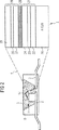
図1には第1の実施例に相応した、本発明による白色光源の断面図が半導体層構造の拡大図とともに示されている。図2には第2の実施例に相応した、本発明による白色光源の断面図が半導体層構造の拡大図とともに示されている。図3には市販されている従来の白色光源の発光スペクトルが示されている。図4には本発明による白色光源の発光スペクトルの例が示されている。
【0017】
図1に相応した本発明による白色光源で、紫外線/青色発光ダイオード1の背面コンタクトは、鑞等の金属性の導電性接続材料、または銀等の導電性接着剤によって第1の電気的接続部2上で固定されている。前面コンタクトは、ボンディングワイヤ9によって第2の電気的接続部3と接続されている。
【0018】
半導体発光ダイオード1の表面と、電気的接続部2および3の領域の一部は露出しており、硬化処理された、波長変換用封かん剤5によって直接的に包囲されている。この封かん剤は、例えば80〜90質量%でエポキシ樹脂から成り、15質量%以下のYAG:Ceから成る発光材料粒子6を含んでいる。通常、これには別の構成成分、例え結合剤、処理補助剤、疎水剤、ミネラルデフューザー並びにチキソトロピー剤が含まれている。
【0019】
図1の右側の部分図には、発光ダイオード1の半導体層構造が拡大され、詳細に示されている。n−型にドーピングされたGaNサブストレート10上にはMOCVD(有機金属CVD)またはMBE(分子線エピタキシー)等の成長方法によって、InGaNから成り、異なるインジウム割合を有する複数の半導体層が被着され、2つの量子井戸単層を構成する。材料InxGa1−xNの禁制帯幅はインジウム割合xの上昇に応じて減少する。
【0020】
比較的少ないインジウム割合xを有する、表向きはドーピングされていないInGaNバリヤ層11がまずは被着される。その上に、インジウム割合xが比較的多いInGaN量子井戸層12が厚さd1で被着される。この量子井戸層12上に、別のInGaNバリヤ層13が続く。このようにして量子井戸層12によって第1の発光領域が形成される。発光領域の発光極大値は、発光領域の厚さやインジウム割合、並びにバリヤ層のインジウム割合によって設定される。ここでバリヤ層13上には、インジウム割合xが比較的少ない、d1より薄い厚さd2の別のInGaN量子井戸層14が被着される。この量子井戸層14上には、再び比較的多いインジウム割合xを有するInGaNバリヤ層15が被着される。その上にはp−型にドーピングされたGaNコンタクト層16が半導体連続層を成層する。
【0021】
このようにして第2の発光領域がInGaN量子井戸層14によって形成される。量子井戸層12および14が同じインジウム割合を有してもよい。その場合に上方の量子井戸層14は、最下の伝導帯と最上の価電子帯との間隔がより大きいので、量子井戸層12よりエネルギー的に高い発光極大値を有する。しかし、量子井戸層12と量子井戸層14とのエネルギー的なシフトを微調整するために、付加的にインジウム割合を変えることもできる。例えば2つの量子井戸層12と14との厚さが同じでも、エネルギー的な離調をインジウム濃度を変えるだけで行うことができる。層構造の光活性領域部分を形成する、層11から層15は表向きはドーピングされていない。
【0022】
エネルギーギャップの光エネルギーがより少ない量子井戸層12が、下方に配置されていることによって、量子井戸層12から発散される光は、より大きいエネルギーギャップを有する上層によって損失されることは殆どなく、発光ダイオード1を包囲する変換封かん剤に達する。
【0023】
図4では図1による白色光源によって得られた、発光スペクトルの例が示されている。この発光スペクトルには量子井戸層12から発散されたビームが別のさらなる線A2として示されている。発光スペクトルのこのような部分は、蛍光体粒子6内で変換されることなく変換材料5を通過した量子井戸層12の放射線によって形成されている。このようにして線A2によって発光スペクトル内のスペクトルホールが埋められ、これにより発光スペクトルの規則的な光強度分布が実現される。
【0024】
このような方法では、2つ以上の量子井戸層を上下に配置することもできる。但しその場合には下方の量子井戸層のビームが、その上方の半導体材料によって吸収されないように常に気をつけなければならない。量子井戸層の禁制帯幅は、半導体層構成が成長する方向に断続的に広くならなければならない。これは、層がより薄くなければならない、および/またはインジウム割合がより少なくなければならないことを意味する。
【0025】
図2には本発明による白色光源の、第2の実施形態の例が断面図で示されている。この実施形態では、例えば2つのpn接合部21および26が垂直方向に上下に積層され、n+P+型トンネル接合部25によって電気的に相互に接続されている。トンネル接合部25は、高濃度(約1020cm−3)にドーピングされたn+型層ないしP+型層から成る。n+型層は隣接するpn接合部のn型領域に接続し、P+型層は他方で隣接するpn接合部のp型領域に接続する。各pn接合部は、活性な発光する中間層23ないし28を有する。
【0026】
詳細にはn型にドーピングされたGaNサブストレート20上に、n型にドーピングされたInGaN層22、p型にドーピングされたInGaN層24、n+P+型トンネル接合部25、n型にドーピングされたInGaN層27、最後にp型にドーピングされたInGaN層29が積層されている。層22と層24との間、また層27と層29との間には光活性領域23ないし28が存在する。これらの光活性領域は、バルクpn接合部を用いる場合、n−型層とp−型層との間にある空乏領域によって形成される。または、そのために被着された量子井戸単層または多重量子井戸層によって形成される。pn接合部21および26がバルクボディから形成される場合、光活性領域23と28との間のエネルギー的な離調は、インジウム割合を介して調整される。これは光活性領域28のインジウム割合がより少ないことを意味する。バルクボディを用いる場合、隣接する層22と24、また27と29が光活性領域23ないし28のように、それぞれ同じインジウム割合を有することもできる。量子井戸単層または多重量子井戸層を用いる場合、第1の実施形態を参照されたい。
【0027】
n+P+型トンネル接合部25は、十分に広いエネルギーギャップを有する材料、例えばGaNから選択されるように注意が必要である、それにより光活性領域23の光ビームの吸収は生じない。
【0028】
また希望により、2つ以上のpn接合部を上下に積層し、n+P+型トンネル接合部25によって電気的に相互に接続することもできる。
【0029】
高濃度にドーピングされたトンネル接合部を使用することによって、半導体発光ダイオード1全体を第2の実施例に従ってモノシリックに、すなわち成長通路内に作製することができるという利点が得られる。しかし択一的に、pn接合部を平坦に相互に鑞接してもよいし、他の方法でpn接合部を金属性コンタクト層によって相互に電気的に接続してもよい。
【0030】
図2に相応する実施例によって、発光スペクトルを図4に相応するようにすることができる。
【0031】
本発明は、SMD(表面実装設計)構成形態に基づく図1および図2に従って説明されているが、いわゆるラジアルダイオードとして同じように実現することもできる。
【図面の簡単な説明】
【図1】 図1には第1の実施例に相応した、本発明による白色光源の断面図が半導体層構造の拡大図とともに示されている。
【図2】 図2には第2の実施例に相応した、本発明による白色光源の断面図が半導体層構造の拡大図とともに示されている。
【図3】 図3には市販されている従来の白色光源の発光スペクトルが示されている。
【図4】 図4には本発明による白色光源の発光スペクトルの例が示されている。
Claims (20)
- 白色光源であって、
該白色光源は半導体発光ダイオード(1)と、
該発光ダイオード(1)を少なくとも部分的に包囲する、透明材料から成る被覆体(5)とを有しており、
ここで前記透明材料には、前記発光ダイオード(1)から発散される光の波長を少なくとも部分的に変換する変換物質(6)が含まれている形式の白色光源において、
前記発光ダイオード(1)は、少なくとも2つの発光領域を有しており、
該2つの発光領域の厚さが異なっているので、当該2つの発光領域の発光スペクトルの極大値(A 1 ,A 2 )はエネルギー的に異なり、かつ前記変換物質(6)の発光スペクトルの1つまたは複数の極大値(B 1 ,B 2 )よりも短い波長を有するように、該2つの発光領域は構成されており、
さらに前記2つの発光領域は、発光スペクトルの極大値のエネルギーが前記発光ダイオード(1)のメインビーム方向で増加するように、前記発光ダイオード(1)のメインビーム方向に相並んで配置されている、ことを特徴とする白色光源。 - 前記発光ダイオード(1)は、pn接合部を厳密に1つ有しており、
前記発光領域は、異なる厚さおよび/または異なる材料組成を有する、相応数の量子井戸単層または多重量子井戸層(12、14)によって構成されている、請求項1記載の白色光源。 - 前記発光ダイオード(1)の発光領域は、相応数のpn接合部(21、26)によって形成されている、請求項1記載の白色光源。
- 前記pn接合部(21、26)は、異なる材料組成を有するバルクボディから形成されている、請求項3記載の白色光源。
- 前記pn接合部(21、26)のうちの少なくとも1つには量子井戸単層または多重量子井戸層が含まれている、請求項3記載の白色光源。
- 前記pn接合部(21、26)にはそれぞれ1つの、量子井戸単層または多重量子井戸層が含まれており、
種々異なるpn接合部の量子井戸層は、様々な厚さおよび/または様々な材料組成を有している、請求項5記載の白色光源。 - 隣接するpn接合部(21、26)は、それぞれn+P+型トンネル接合部(25)によって相互にコンタクトされており、
該n+P+型トンネル接合部は、n+型にドーピングされた層と、該n+型にドーピングされた層に当接しているp+型にドーピングされた層とから成り、
ここでこのn+型にドーピングされた層は、一方のpn接合部(21)のn型領域と接続しており、
p+型にドーピングされた層は、別のpn接合部(26)のp型領域と接続しており、
n+ドーピング濃度ないしはp+ドーピング濃度は、前記トンネル接合部の電気抵抗が比較的低くなるように選択されている、請求項3記載の白色光源。 - 前記半導体発光ダイオード(1)全体はモノリシックに作製されている、請求項7記載の白色光源。
- 隣接するpn接合部(21、26)はそれぞれ、鑞接層等の金属性コンタクト層によって相互に電気的に接続されている、請求項3から6までのいずれか1項記載の白色光源。
- 前記半導体発光ダイオード(1)は、GaNまたはInGaNをベースにして形成されている、請求項1記載の白色光源。
- 前記半導体発光ダイオード(1)は、紫外線/青色発光の半導体発光ダイオード(1)である、請求項1記載の白色光源。
- 前記白色光源の広帯域の発光スペクトルが形成される、請求項1記載の白色光源。
- 前記複数の発光領域はエネルギー的なシフトのために、付加的に、異なる材料組成で構成されている、請求項1記載の白色光源。
- 前記複数の発光領域は、異なる厚さおよび異なるインジウム濃度を有している、請求項12記載の白色光源。
- 前記複数の発光領域は、共通のサブストレート上に、かつ2つの電気的な外部コンタクト層の間に配置されており、当該発光領域は共通の電圧源と接続される、請求項1記載の白色光源。
- 前記複数の発光領域はそれぞれ、比較的広いエネルギーギャップを有する2つの層の間にそれぞれはめ込まれ、相並んで配置されている、請求項1記載の白色光源。
- 前記被覆体は80〜90質量%でエポキシ樹脂から成り、15質量%以下のYAG:Ceから成る発光材料粒子(6)を含んでいる、請求項1記載の白色光源。
- 前記被覆体内に別の構成成分が含まれている、請求項17記載の白色光源。
- 前記別の構成成分は、結合剤、処理補助剤、疎水剤、ミネラルデフューザーおよび/またはチキソトロピー剤である、請求項18記載の白色光源。
- 前記半導体発光ダイオード(1)の層は、有機金属気相成長法または分子線エピタキシーによって、GaNサブストレート(10)上に析出される、請求項1記載の白色光源。
Applications Claiming Priority (3)
| Application Number | Priority Date | Filing Date | Title |
|---|---|---|---|
| DE19952932A DE19952932C1 (de) | 1999-11-03 | 1999-11-03 | LED-Weißlichtquelle mit breitbandiger Anregung |
| DE19952932.9 | 1999-11-03 | ||
| PCT/DE2000/003520 WO2001033640A1 (de) | 1999-11-03 | 2000-10-06 | Led-weisslichtquelle mit breitbandiger anregung |
Publications (3)
| Publication Number | Publication Date |
|---|---|
| JP2003513474A JP2003513474A (ja) | 2003-04-08 |
| JP2003513474A5 JP2003513474A5 (ja) | 2011-01-13 |
| JP4681184B2 true JP4681184B2 (ja) | 2011-05-11 |
Family
ID=7927797
Family Applications (1)
| Application Number | Title | Priority Date | Filing Date |
|---|---|---|---|
| JP2001535238A Expired - Lifetime JP4681184B2 (ja) | 1999-11-03 | 2000-10-06 | 広帯域な励起を有する発光ダイオード白色光源 |
Country Status (5)
| Country | Link |
|---|---|
| US (1) | US6734467B2 (ja) |
| JP (1) | JP4681184B2 (ja) |
| DE (1) | DE19952932C1 (ja) |
| TW (1) | TW476166B (ja) |
| WO (1) | WO2001033640A1 (ja) |
Families Citing this family (78)
| Publication number | Priority date | Publication date | Assignee | Title |
|---|---|---|---|---|
| JP3404064B2 (ja) * | 1993-03-09 | 2003-05-06 | 株式会社日立製作所 | 半導体装置及びその製造方法 |
| US6633120B2 (en) | 1998-11-19 | 2003-10-14 | Unisplay S.A. | LED lamps |
| GB2366074A (en) * | 2000-02-15 | 2002-02-27 | Hassan Paddy Abdel Salam | LED light source with two vertically-stacked LEDs of different colours |
| US7768210B2 (en) * | 1999-12-22 | 2010-08-03 | General Electric Company | Hybrid electroluminescent devices |
| AUPQ818100A0 (en) * | 2000-06-15 | 2000-07-06 | Arlec Australia Limited | Led lamp |
| KR20040029385A (ko) * | 2001-08-01 | 2004-04-06 | 남 영 김 | 화상표시장치 |
| WO2003017320A1 (en) * | 2001-08-21 | 2003-02-27 | Nam-Young Kim | Lamp utilizing a light emitted diode |
| US6970512B2 (en) | 2001-08-28 | 2005-11-29 | Sbc Technology Resources, Inc. | Method and system to improve the transport of compressed video data |
| JP4307113B2 (ja) * | 2002-03-19 | 2009-08-05 | 宣彦 澤木 | 半導体発光素子およびその製造方法 |
| DE10214951A1 (de) * | 2002-04-04 | 2003-05-22 | G L I Global Light Ind Gmbh | Lichtabstrahlendes Halbleiterbauelement |
| US6841802B2 (en) | 2002-06-26 | 2005-01-11 | Oriol, Inc. | Thin film light emitting diode |
| US6822991B2 (en) * | 2002-09-30 | 2004-11-23 | Lumileds Lighting U.S., Llc | Light emitting devices including tunnel junctions |
| US6806658B2 (en) * | 2003-03-07 | 2004-10-19 | Agilent Technologies, Inc. | Method for making an LED |
| KR101148332B1 (ko) * | 2003-04-30 | 2012-05-25 | 크리, 인코포레이티드 | 콤팩트 광학 특성을 지닌 높은 전력의 발광 소자 패키지 |
| US7005679B2 (en) | 2003-05-01 | 2006-02-28 | Cree, Inc. | Multiple component solid state white light |
| US7906790B2 (en) | 2003-06-24 | 2011-03-15 | GE Lighting Solutions, LLC | Full spectrum phosphor blends for white light generation with LED chips |
| JP4699681B2 (ja) * | 2003-06-27 | 2011-06-15 | パナソニック株式会社 | Ledモジュール、および照明装置 |
| TW200525779A (en) * | 2004-01-27 | 2005-08-01 | Super Nova Optoelectronics Corp | White-like light emitting device and its manufacturing method |
| DE102004004765A1 (de) * | 2004-01-29 | 2005-09-01 | Rwe Space Solar Power Gmbh | Aktive Zonen aufweisende Halbleiterstruktur |
| DE102005020695B4 (de) * | 2004-04-30 | 2006-06-22 | Optotransmitter-Umweltschutz-Technologie E.V. | Vorrichtung zur Emission von Strahlung mit einstellbarer Spektraleigenschaft |
| KR101433343B1 (ko) * | 2004-05-05 | 2014-08-22 | 렌슬러 폴리테크닉 인스티튜트 | 고체-상태 에미터 및 하향-변환 재료를 이용한 고효율 광 소스 |
| US7837348B2 (en) | 2004-05-05 | 2010-11-23 | Rensselaer Polytechnic Institute | Lighting system using multiple colored light emitting sources and diffuser element |
| US7534633B2 (en) * | 2004-07-02 | 2009-05-19 | Cree, Inc. | LED with substrate modifications for enhanced light extraction and method of making same |
| EP1769050B1 (en) * | 2004-07-06 | 2013-01-16 | Lightscape Materials Inc. | Efficient, green-emitting phosphors, and combinations with red-emitting phosphors |
| US20060012289A1 (en) * | 2004-07-19 | 2006-01-19 | General Electric Company | Hybrid electroluminescent devices |
| US7323721B2 (en) * | 2004-09-09 | 2008-01-29 | Blue Photonics Inc. | Monolithic multi-color, multi-quantum well semiconductor LED |
| US7745814B2 (en) * | 2004-12-09 | 2010-06-29 | 3M Innovative Properties Company | Polychromatic LED's and related semiconductor devices |
| US7719015B2 (en) * | 2004-12-09 | 2010-05-18 | 3M Innovative Properties Company | Type II broadband or polychromatic LED's |
| US7402831B2 (en) * | 2004-12-09 | 2008-07-22 | 3M Innovative Properties Company | Adapting short-wavelength LED's for polychromatic, broadband, or “white” emission |
| TWI247439B (en) * | 2004-12-17 | 2006-01-11 | Genesis Photonics Inc | Light-emitting diode device |
| CN1684279A (zh) * | 2005-02-25 | 2005-10-19 | 炬鑫科技股份有限公司 | 发光元件 |
| FR2883653B1 (fr) * | 2005-03-22 | 2007-05-25 | Gemplus Sa | Module electronique et carte a puce avec indicateur lumineux |
| US7276183B2 (en) * | 2005-03-25 | 2007-10-02 | Sarnoff Corporation | Metal silicate-silica-based polymorphous phosphors and lighting devices |
| US7690167B2 (en) * | 2005-04-28 | 2010-04-06 | Antonic James P | Structural support framing assembly |
| TWM279023U (en) * | 2005-04-29 | 2005-10-21 | Super Nova Optoelectronics Cor | White light emitting diode device |
| CN100508223C (zh) * | 2005-05-24 | 2009-07-01 | 新世纪光电股份有限公司 | 二极管发光装置 |
| CN100508224C (zh) * | 2005-06-13 | 2009-07-01 | 新世纪光电股份有限公司 | 具有发光二极管的白光装置 |
| CN101138104B (zh) * | 2005-06-23 | 2011-08-24 | 伦斯勒工业学院 | 利用短波长led和下变频材料产生白光的封装设计 |
| JP5285835B2 (ja) * | 2005-07-13 | 2013-09-11 | 株式会社東芝 | 半導体素子およびその製造方法 |
| BRPI0618866A2 (pt) * | 2005-11-24 | 2016-09-06 | Koninkl Philips Electronics Nv | construção de diodo emissor de luz (led), método para ajuste do valor de saída de temperatura de cor de uma construção de led, e, meio para ajuste de uma temperatura de cor resultante de uma construção de led |
| US20070125984A1 (en) * | 2005-12-01 | 2007-06-07 | Sarnoff Corporation | Phosphors protected against moisture and LED lighting devices |
| US8906262B2 (en) * | 2005-12-02 | 2014-12-09 | Lightscape Materials, Inc. | Metal silicate halide phosphors and LED lighting devices using the same |
| US20070145879A1 (en) * | 2005-12-22 | 2007-06-28 | Abramov Vladimir S | Light emitting halogen-silicate photophosphor compositions and systems |
| JP2009527071A (ja) | 2005-12-22 | 2009-07-23 | クリー エル イー ディー ライティング ソリューションズ インコーポレイテッド | 照明装置 |
| KR20080106402A (ko) | 2006-01-05 | 2008-12-05 | 일루미텍스, 인크. | Led로부터 광을 유도하기 위한 개별 광학 디바이스 |
| JP2007266579A (ja) * | 2006-02-28 | 2007-10-11 | Toshiba Lighting & Technology Corp | 発光装置 |
| JP2007281257A (ja) * | 2006-04-07 | 2007-10-25 | Toyoda Gosei Co Ltd | Iii族窒化物半導体発光素子 |
| CN102437152A (zh) | 2006-04-24 | 2012-05-02 | 克利公司 | 侧视表面安装式白光led |
| US7952110B2 (en) * | 2006-06-12 | 2011-05-31 | 3M Innovative Properties Company | LED device with re-emitting semiconductor construction and converging optical element |
| WO2007146861A1 (en) * | 2006-06-12 | 2007-12-21 | 3M Innovative Properties Company | Led device with re-emitting semiconductor construction and converging optical element |
| US7863634B2 (en) * | 2006-06-12 | 2011-01-04 | 3M Innovative Properties Company | LED device with re-emitting semiconductor construction and reflector |
| US20070284565A1 (en) * | 2006-06-12 | 2007-12-13 | 3M Innovative Properties Company | Led device with re-emitting semiconductor construction and optical element |
| US7902542B2 (en) * | 2006-06-14 | 2011-03-08 | 3M Innovative Properties Company | Adapted LED device with re-emitting semiconductor construction |
| US7703942B2 (en) * | 2006-08-31 | 2010-04-27 | Rensselaer Polytechnic Institute | High-efficient light engines using light emitting diodes |
| US20100224890A1 (en) * | 2006-09-18 | 2010-09-09 | Cree, Inc. | Light emitting diode chip with electrical insulation element |
| EP2070123A2 (en) | 2006-10-02 | 2009-06-17 | Illumitex, Inc. | Led system and method |
| CN101605867B (zh) * | 2006-10-03 | 2013-05-08 | 渲染材料公司 | 金属硅酸盐卤化物磷光体以及使用它们的led照明器件 |
| US7889421B2 (en) * | 2006-11-17 | 2011-02-15 | Rensselaer Polytechnic Institute | High-power white LEDs and manufacturing method thereof |
| US20080197369A1 (en) * | 2007-02-20 | 2008-08-21 | Cree, Inc. | Double flip semiconductor device and method for fabrication |
| US10256385B2 (en) | 2007-10-31 | 2019-04-09 | Cree, Inc. | Light emitting die (LED) packages and related methods |
| US9431589B2 (en) * | 2007-12-14 | 2016-08-30 | Cree, Inc. | Textured encapsulant surface in LED packages |
| US20090159915A1 (en) * | 2007-12-19 | 2009-06-25 | Shaul Branchevsky | Led insert module and multi-layer lens |
| US8178888B2 (en) * | 2008-02-01 | 2012-05-15 | Cree, Inc. | Semiconductor light emitting devices with high color rendering |
| EP2240968A1 (en) | 2008-02-08 | 2010-10-20 | Illumitex, Inc. | System and method for emitter layer shaping |
| CN103715318A (zh) | 2008-02-15 | 2014-04-09 | 克里公司 | 用于提供白色光输出的宽带发光器件灯 |
| TW201034256A (en) | 2008-12-11 | 2010-09-16 | Illumitex Inc | Systems and methods for packaging light-emitting diode devices |
| US8585253B2 (en) | 2009-08-20 | 2013-11-19 | Illumitex, Inc. | System and method for color mixing lens array |
| US8449128B2 (en) | 2009-08-20 | 2013-05-28 | Illumitex, Inc. | System and method for a lens and phosphor layer |
| US8575592B2 (en) * | 2010-02-03 | 2013-11-05 | Cree, Inc. | Group III nitride based light emitting diode structures with multiple quantum well structures having varying well thicknesses |
| US9331252B2 (en) | 2011-08-23 | 2016-05-03 | Micron Technology, Inc. | Wavelength converters, including polarization-enhanced carrier capture converters, for solid state lighting devices, and associated systems and methods |
| CN104160212B (zh) * | 2012-03-01 | 2018-10-12 | 飞利浦灯具控股公司 | Led照明布置 |
| FR3004005B1 (fr) * | 2013-03-28 | 2016-11-25 | Commissariat Energie Atomique | Diode electroluminescente a multiples puits quantiques et jonction p-n asymetrique |
| DE102013104954A1 (de) | 2013-05-14 | 2014-11-20 | Osram Opto Semiconductors Gmbh | Optoelektronisches Bauelement und Verfahren zu seiner Herstellung |
| CN104241262B (zh) | 2013-06-14 | 2020-11-06 | 惠州科锐半导体照明有限公司 | 发光装置以及显示装置 |
| US9601656B1 (en) * | 2014-06-13 | 2017-03-21 | Silego Technology, Inc. | Method of manufacturing low cost, high efficiency LED |
| US10054485B2 (en) | 2016-03-17 | 2018-08-21 | Raytheon Company | UV LED-phosphor based hyperspectral calibrator |
| US10371325B1 (en) * | 2018-06-25 | 2019-08-06 | Intematix Corporation | Full spectrum white light emitting devices |
| JP7101347B2 (ja) | 2019-12-27 | 2022-07-15 | 日亜化学工業株式会社 | 発光素子の製造方法 |
Citations (4)
| Publication number | Priority date | Publication date | Assignee | Title |
|---|---|---|---|---|
| US3875473A (en) * | 1972-12-13 | 1975-04-01 | Philips Corp | Polychromatic electroluminescent device |
| WO1998012757A1 (de) * | 1996-09-20 | 1998-03-26 | Siemens Aktiengesellschaft | Wellenlängenkonvertierende vergussmasse, deren verwendung und verfahren zu deren herstellung |
| US5851905A (en) * | 1996-07-11 | 1998-12-22 | North Carolina State University | Methods of forming indium gallium nitride or aluminum indium gallium nitride using controlled hydrogen gas flows |
| JP2001196645A (ja) * | 1999-10-25 | 2001-07-19 | Nichia Chem Ind Ltd | 発光装置 |
Family Cites Families (8)
| Publication number | Priority date | Publication date | Assignee | Title |
|---|---|---|---|---|
| JPS48102585A (ja) * | 1972-04-04 | 1973-12-22 | ||
| DE3804293A1 (de) * | 1988-02-12 | 1989-08-24 | Philips Patentverwaltung | Anordnung mit einer elektrolumineszenz- oder laserdiode |
| JPH0710003B2 (ja) * | 1988-03-11 | 1995-02-01 | 信越半導体株式会社 | 混色発光半導体素子 |
| JP3649748B2 (ja) * | 1993-03-22 | 2005-05-18 | 三洋電機株式会社 | 発光ダイオードランプ |
| JPH08335718A (ja) * | 1995-06-08 | 1996-12-17 | Daido Steel Co Ltd | 発光ダイオード |
| JP3543498B2 (ja) * | 1996-06-28 | 2004-07-14 | 豊田合成株式会社 | 3族窒化物半導体発光素子 |
| US5813753A (en) * | 1997-05-27 | 1998-09-29 | Philips Electronics North America Corporation | UV/blue led-phosphor device with efficient conversion of UV/blues light to visible light |
| DE29914941U1 (de) * | 1999-08-26 | 1999-11-25 | Everlight Electronics Co | Mit LED's arbeitende Farb-Mischvorrichtung |
-
1999
- 1999-11-03 DE DE19952932A patent/DE19952932C1/de not_active Expired - Lifetime
-
2000
- 2000-10-06 JP JP2001535238A patent/JP4681184B2/ja not_active Expired - Lifetime
- 2000-10-06 WO PCT/DE2000/003520 patent/WO2001033640A1/de active Application Filing
- 2000-10-26 TW TW089122534A patent/TW476166B/zh not_active IP Right Cessation
-
2002
- 2002-05-03 US US10/137,885 patent/US6734467B2/en not_active Expired - Lifetime
Patent Citations (4)
| Publication number | Priority date | Publication date | Assignee | Title |
|---|---|---|---|---|
| US3875473A (en) * | 1972-12-13 | 1975-04-01 | Philips Corp | Polychromatic electroluminescent device |
| US5851905A (en) * | 1996-07-11 | 1998-12-22 | North Carolina State University | Methods of forming indium gallium nitride or aluminum indium gallium nitride using controlled hydrogen gas flows |
| WO1998012757A1 (de) * | 1996-09-20 | 1998-03-26 | Siemens Aktiengesellschaft | Wellenlängenkonvertierende vergussmasse, deren verwendung und verfahren zu deren herstellung |
| JP2001196645A (ja) * | 1999-10-25 | 2001-07-19 | Nichia Chem Ind Ltd | 発光装置 |
Also Published As
| Publication number | Publication date |
|---|---|
| WO2001033640A1 (de) | 2001-05-10 |
| DE19952932C1 (de) | 2001-05-03 |
| TW476166B (en) | 2002-02-11 |
| US6734467B2 (en) | 2004-05-11 |
| JP2003513474A (ja) | 2003-04-08 |
| US20020167014A1 (en) | 2002-11-14 |
Similar Documents
| Publication | Publication Date | Title |
|---|---|---|
| JP4681184B2 (ja) | 広帯域な励起を有する発光ダイオード白色光源 | |
| JP4101468B2 (ja) | 発光装置の製造方法 | |
| Schlotter et al. | Fabrication and characterization of GaN/InGaN/AlGaN double heterostructure LEDs and their application in luminescence conversion LEDs | |
| US10930817B2 (en) | Light-emitting device | |
| US20080210958A1 (en) | Semiconductor white light emitting device and method for manufacturing the same | |
| US20110012141A1 (en) | Single-color wavelength-converted light emitting devices | |
| KR20090060358A (ko) | Led 반도체 소자 및 그의 이용 | |
| JP5289448B2 (ja) | 放射放出用の半導体ボディ | |
| DE202011110024U1 (de) | Weisslichtgerät | |
| EP1528604A2 (en) | Semiconductor light emitting devices with enhanced luminous efficiency | |
| EP3201953B1 (en) | Light source with tunable emission spectrum | |
| JP2002170999A (ja) | 発光装置及びその製造方法 | |
| US20110141716A1 (en) | Illumination Device for Backlighting a Display, and a Display Comprising such an Illumination Device | |
| CN107565009A (zh) | Led模块 | |
| KR100422944B1 (ko) | 반도체 엘이디(led) 소자 | |
| KR100433989B1 (ko) | 반도체 엘이디 소자 및 그 제조방법 | |
| KR20110117415A (ko) | 반도체 발광소자, 반도체 발광소자 패키지 및 반도체 발광소자의 제조방법 | |
| US10510925B2 (en) | Light-emitting device and lighting system comprising same | |
| JP2008041807A (ja) | 白色光源 | |
| KR100573488B1 (ko) | 발광장치 | |
| US10199534B2 (en) | Light-emitting diode, light-emitting diode package, and lighting system including same | |
| KR100665174B1 (ko) | 반도체 발광 소자 | |
| KR102423748B1 (ko) | 발광장치 | |
| TW202021155A (zh) | 具有光散射調諧之發光器件以控制色彩偏移 | |
| JPH11204836A (ja) | 半導体発光素子 |
Legal Events
| Date | Code | Title | Description |
|---|---|---|---|
| A621 | Written request for application examination |
Free format text: JAPANESE INTERMEDIATE CODE: A621 Effective date: 20071003 |
|
| A131 | Notification of reasons for refusal |
Free format text: JAPANESE INTERMEDIATE CODE: A131 Effective date: 20100818 |
|
| A524 | Written submission of copy of amendment under section 19 (pct) |
Free format text: JAPANESE INTERMEDIATE CODE: A524 Effective date: 20101117 |
|
| A521 | Written amendment |
Free format text: JAPANESE INTERMEDIATE CODE: A523 Effective date: 20101118 |
|
| TRDD | Decision of grant or rejection written | ||
| RD04 | Notification of resignation of power of attorney |
Free format text: JAPANESE INTERMEDIATE CODE: A7424 Effective date: 20101228 |
|
| A01 | Written decision to grant a patent or to grant a registration (utility model) |
Free format text: JAPANESE INTERMEDIATE CODE: A01 Effective date: 20110107 |
|
| A01 | Written decision to grant a patent or to grant a registration (utility model) |
Free format text: JAPANESE INTERMEDIATE CODE: A01 |
|
| A61 | First payment of annual fees (during grant procedure) |
Free format text: JAPANESE INTERMEDIATE CODE: A61 Effective date: 20110204 |
|
| R150 | Certificate of patent or registration of utility model |
Ref document number: 4681184 Country of ref document: JP Free format text: JAPANESE INTERMEDIATE CODE: R150 Free format text: JAPANESE INTERMEDIATE CODE: R150 |
|
| FPAY | Renewal fee payment (event date is renewal date of database) |
Free format text: PAYMENT UNTIL: 20140210 Year of fee payment: 3 |
|
| R250 | Receipt of annual fees |
Free format text: JAPANESE INTERMEDIATE CODE: R250 |
|
| R250 | Receipt of annual fees |
Free format text: JAPANESE INTERMEDIATE CODE: R250 |
|
| R250 | Receipt of annual fees |
Free format text: JAPANESE INTERMEDIATE CODE: R250 |
|
| R250 | Receipt of annual fees |
Free format text: JAPANESE INTERMEDIATE CODE: R250 |
|
| R250 | Receipt of annual fees |
Free format text: JAPANESE INTERMEDIATE CODE: R250 |
|
| R250 | Receipt of annual fees |
Free format text: JAPANESE INTERMEDIATE CODE: R250 |
|
| R250 | Receipt of annual fees |
Free format text: JAPANESE INTERMEDIATE CODE: R250 |