JP4660552B2 - 表示パネル用の基板とこの基板を備える表示パネル - Google Patents
表示パネル用の基板とこの基板を備える表示パネル Download PDFInfo
- Publication number
- JP4660552B2 JP4660552B2 JP2007536469A JP2007536469A JP4660552B2 JP 4660552 B2 JP4660552 B2 JP 4660552B2 JP 2007536469 A JP2007536469 A JP 2007536469A JP 2007536469 A JP2007536469 A JP 2007536469A JP 4660552 B2 JP4660552 B2 JP 4660552B2
- Authority
- JP
- Japan
- Prior art keywords
- pattern
- signal line
- line
- display panel
- substrate
- Prior art date
- Legal status (The legal status is an assumption and is not a legal conclusion. Google has not performed a legal analysis and makes no representation as to the accuracy of the status listed.)
- Expired - Fee Related
Links
Images

Classifications
-
- G—PHYSICS
- G02—OPTICS
- G02F—OPTICAL DEVICES OR ARRANGEMENTS FOR THE CONTROL OF LIGHT BY MODIFICATION OF THE OPTICAL PROPERTIES OF THE MEDIA OF THE ELEMENTS INVOLVED THEREIN; NON-LINEAR OPTICS; FREQUENCY-CHANGING OF LIGHT; OPTICAL LOGIC ELEMENTS; OPTICAL ANALOGUE/DIGITAL CONVERTERS
- G02F1/00—Devices or arrangements for the control of the intensity, colour, phase, polarisation or direction of light arriving from an independent light source, e.g. switching, gating or modulating; Non-linear optics
- G02F1/01—Devices or arrangements for the control of the intensity, colour, phase, polarisation or direction of light arriving from an independent light source, e.g. switching, gating or modulating; Non-linear optics for the control of the intensity, phase, polarisation or colour
- G02F1/13—Devices or arrangements for the control of the intensity, colour, phase, polarisation or direction of light arriving from an independent light source, e.g. switching, gating or modulating; Non-linear optics for the control of the intensity, phase, polarisation or colour based on liquid crystals, e.g. single liquid crystal display cells
- G02F1/133—Constructional arrangements; Operation of liquid crystal cells; Circuit arrangements
- G02F1/136—Liquid crystal cells structurally associated with a semi-conducting layer or substrate, e.g. cells forming part of an integrated circuit
- G02F1/1362—Active matrix addressed cells
-
- G—PHYSICS
- G02—OPTICS
- G02F—OPTICAL DEVICES OR ARRANGEMENTS FOR THE CONTROL OF LIGHT BY MODIFICATION OF THE OPTICAL PROPERTIES OF THE MEDIA OF THE ELEMENTS INVOLVED THEREIN; NON-LINEAR OPTICS; FREQUENCY-CHANGING OF LIGHT; OPTICAL LOGIC ELEMENTS; OPTICAL ANALOGUE/DIGITAL CONVERTERS
- G02F1/00—Devices or arrangements for the control of the intensity, colour, phase, polarisation or direction of light arriving from an independent light source, e.g. switching, gating or modulating; Non-linear optics
- G02F1/01—Devices or arrangements for the control of the intensity, colour, phase, polarisation or direction of light arriving from an independent light source, e.g. switching, gating or modulating; Non-linear optics for the control of the intensity, phase, polarisation or colour
- G02F1/13—Devices or arrangements for the control of the intensity, colour, phase, polarisation or direction of light arriving from an independent light source, e.g. switching, gating or modulating; Non-linear optics for the control of the intensity, phase, polarisation or colour based on liquid crystals, e.g. single liquid crystal display cells
- G02F1/133—Constructional arrangements; Operation of liquid crystal cells; Circuit arrangements
- G02F1/1333—Constructional arrangements; Manufacturing methods
- G02F1/133354—Arrangements for aligning or assembling substrates
-
- G—PHYSICS
- G02—OPTICS
- G02F—OPTICAL DEVICES OR ARRANGEMENTS FOR THE CONTROL OF LIGHT BY MODIFICATION OF THE OPTICAL PROPERTIES OF THE MEDIA OF THE ELEMENTS INVOLVED THEREIN; NON-LINEAR OPTICS; FREQUENCY-CHANGING OF LIGHT; OPTICAL LOGIC ELEMENTS; OPTICAL ANALOGUE/DIGITAL CONVERTERS
- G02F1/00—Devices or arrangements for the control of the intensity, colour, phase, polarisation or direction of light arriving from an independent light source, e.g. switching, gating or modulating; Non-linear optics
- G02F1/01—Devices or arrangements for the control of the intensity, colour, phase, polarisation or direction of light arriving from an independent light source, e.g. switching, gating or modulating; Non-linear optics for the control of the intensity, phase, polarisation or colour
- G02F1/13—Devices or arrangements for the control of the intensity, colour, phase, polarisation or direction of light arriving from an independent light source, e.g. switching, gating or modulating; Non-linear optics for the control of the intensity, phase, polarisation or colour based on liquid crystals, e.g. single liquid crystal display cells
- G02F1/133—Constructional arrangements; Operation of liquid crystal cells; Circuit arrangements
- G02F1/136—Liquid crystal cells structurally associated with a semi-conducting layer or substrate, e.g. cells forming part of an integrated circuit
- G02F1/1362—Active matrix addressed cells
- G02F1/136231—Active matrix addressed cells for reducing the number of lithographic steps
-
- Y—GENERAL TAGGING OF NEW TECHNOLOGICAL DEVELOPMENTS; GENERAL TAGGING OF CROSS-SECTIONAL TECHNOLOGIES SPANNING OVER SEVERAL SECTIONS OF THE IPC; TECHNICAL SUBJECTS COVERED BY FORMER USPC CROSS-REFERENCE ART COLLECTIONS [XRACs] AND DIGESTS
- Y10—TECHNICAL SUBJECTS COVERED BY FORMER USPC
- Y10T—TECHNICAL SUBJECTS COVERED BY FORMER US CLASSIFICATION
- Y10T428/00—Stock material or miscellaneous articles
- Y10T428/24—Structurally defined web or sheet [e.g., overall dimension, etc.]
- Y10T428/24802—Discontinuous or differential coating, impregnation or bond [e.g., artwork, printing, retouched photograph, etc.]
Landscapes
- Physics & Mathematics (AREA)
- Nonlinear Science (AREA)
- Engineering & Computer Science (AREA)
- Microelectronics & Electronic Packaging (AREA)
- Mathematical Physics (AREA)
- Chemical & Material Sciences (AREA)
- Crystallography & Structural Chemistry (AREA)
- General Physics & Mathematics (AREA)
- Optics & Photonics (AREA)
- Liquid Crystal (AREA)
- Devices For Indicating Variable Information By Combining Individual Elements (AREA)
Description
Claims (4)
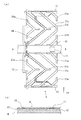
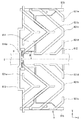
- 基板の表面にゲート信号線のパターンと、ソース信号線のパターンおよびドレイン線のパターンとが絶縁層を挟んで積層状に形成される表示パネル用の基板であって、前記ゲート信号線のパターンと、前記ソース信号線のパターンおよび前記ドレイン線のパターンとの位置合わせ精度を測定するための位置測定マークが前記ゲート信号線のパターンに重畳する位置に浮島状に形成されることを特徴とする表示パネル用の基板。
- 前記位置測定マークは、前記ソース信号線のパターンおよび前記ドレイン線のパターンが形成される層と同じ層に形成されることを特徴とする請求項1に記載の表示パネル用の基板。
- 前記位置測定マークは、少なくとも一辺以上の直線部分を含む形状であることを特徴とする請求項1または請求項2に記載の表示パネル用の基板。
- 請求項1から請求項3のいずれか一項に記載の表示パネル用の基板を備えることを特徴とする表示パネル。
Applications Claiming Priority (3)
| Application Number | Priority Date | Filing Date | Title |
|---|---|---|---|
| JP2005275640 | 2005-09-22 | ||
| JP2005275640 | 2005-09-22 | ||
| PCT/JP2006/318331 WO2007034740A1 (ja) | 2005-09-22 | 2006-09-15 | 表示パネル用の基板とこの基板を備える表示パネル |
Publications (2)
| Publication Number | Publication Date |
|---|---|
| JPWO2007034740A1 JPWO2007034740A1 (ja) | 2009-03-26 |
| JP4660552B2 true JP4660552B2 (ja) | 2011-03-30 |
Family
ID=37888785
Family Applications (1)
| Application Number | Title | Priority Date | Filing Date |
|---|---|---|---|
| JP2007536469A Expired - Fee Related JP4660552B2 (ja) | 2005-09-22 | 2006-09-15 | 表示パネル用の基板とこの基板を備える表示パネル |
Country Status (4)
| Country | Link |
|---|---|
| US (3) | US8022559B2 (ja) |
| JP (1) | JP4660552B2 (ja) |
| CN (1) | CN101268415A (ja) |
| WO (1) | WO2007034740A1 (ja) |
Families Citing this family (3)
| Publication number | Priority date | Publication date | Assignee | Title |
|---|---|---|---|---|
| CN102646629B (zh) * | 2011-07-05 | 2014-04-02 | 北京京东方光电科技有限公司 | 一种阵列基板及其制造方法 |
| CN105511126B (zh) * | 2016-01-21 | 2018-11-13 | 京东方科技集团股份有限公司 | 显示面板及其制备方法和检测方法 |
| KR102673361B1 (ko) * | 2019-08-02 | 2024-06-13 | 삼성디스플레이 주식회사 | 표시 장치 |
Citations (2)
| Publication number | Priority date | Publication date | Assignee | Title |
|---|---|---|---|---|
| JPH05323342A (ja) * | 1992-05-19 | 1993-12-07 | Casio Comput Co Ltd | 導電性パターン形成パネル |
| JP2003302654A (ja) * | 2002-04-12 | 2003-10-24 | Hitachi Ltd | 表示装置 |
Family Cites Families (18)
| Publication number | Priority date | Publication date | Assignee | Title |
|---|---|---|---|---|
| JPH04294329A (ja) | 1991-03-22 | 1992-10-19 | G T C:Kk | 液晶表示装置およびその製造方法 |
| TW543787U (en) * | 1996-03-29 | 2003-07-21 | Toshiba Corp | Liquid crystal display apparatus |
| US6204895B1 (en) * | 1997-09-30 | 2001-03-20 | Kabushiki Kaisha Toshiba | Display panel associated with light collecting plate and position adjusting method using microlenses for the display panel |
| JP3538073B2 (ja) * | 1999-07-29 | 2004-06-14 | Nec液晶テクノロジー株式会社 | Tftを搭載する基板側に色層を有するアクティブマトリクス型液晶表示装置及びその製造方法 |
| JP2001148480A (ja) * | 1999-11-18 | 2001-05-29 | Nec Corp | 薄膜トランジスタ、薄膜トランジスタの製造装置、および薄膜トランジスタその製造方法 |
| JP4884586B2 (ja) * | 2000-12-18 | 2012-02-29 | 株式会社 日立ディスプレイズ | 液晶表示装置 |
| JP2002221735A (ja) * | 2001-01-26 | 2002-08-09 | Matsushita Electric Ind Co Ltd | アクティブマトリクス基板、液晶表示装置、および、それらの製造方法 |
| JP2003058073A (ja) * | 2001-08-08 | 2003-02-28 | Seiko Epson Corp | 電気光学装置の製造方法、電気光学装置、および電子機器 |
| KR100801151B1 (ko) * | 2001-10-04 | 2008-02-05 | 엘지.필립스 엘시디 주식회사 | 액정표시장치용 블랙매트릭스 |
| JP3992976B2 (ja) * | 2001-12-21 | 2007-10-17 | 株式会社半導体エネルギー研究所 | 半導体装置の作製方法 |
| JP2003209041A (ja) * | 2002-01-15 | 2003-07-25 | Seiko Epson Corp | パターンの位置合わせ精度測定方法、パターンの形成方法、電気光学装置の製造方法、半導体装置の製造方法 |
| TWI310849B (en) * | 2002-02-06 | 2009-06-11 | Au Optronics Corp | Pixel structure |
| JP2004054069A (ja) * | 2002-07-23 | 2004-02-19 | Advanced Display Inc | 表示装置及び表示装置の断線修復方法 |
| JP2004304083A (ja) * | 2003-03-31 | 2004-10-28 | Seiko Epson Corp | パターニング精度測定方法、パターンの形成方法、薄膜トランジスタの製造方法、半導体装置の製造方法、電気光学装置、および電子機器 |
| JP2004317728A (ja) * | 2003-04-15 | 2004-11-11 | Seiko Epson Corp | アライメントマーク付き基板及びその製造方法並びに電気光学装置用基板及び電気光学装置 |
| JP4522145B2 (ja) | 2004-05-25 | 2010-08-11 | シャープ株式会社 | 表示装置用基板、その製造方法及び表示装置 |
| TW200638143A (en) * | 2004-10-29 | 2006-11-01 | Toshiba Matsushita Display Tec | Display device |
| KR101140241B1 (ko) * | 2005-06-27 | 2012-04-26 | 엘지디스플레이 주식회사 | 얼라인 마크를 포함한 액정표시소자 |
-
2006
- 2006-09-15 CN CNA2006800348352A patent/CN101268415A/zh active Pending
- 2006-09-15 US US12/067,518 patent/US8022559B2/en active Active
- 2006-09-15 JP JP2007536469A patent/JP4660552B2/ja not_active Expired - Fee Related
- 2006-09-15 WO PCT/JP2006/318331 patent/WO2007034740A1/ja not_active Ceased
-
2010
- 2010-12-30 US US12/981,699 patent/US8008789B2/en active Active
-
2011
- 2011-07-14 US US13/182,466 patent/US8193649B2/en active Active
Patent Citations (2)
| Publication number | Priority date | Publication date | Assignee | Title |
|---|---|---|---|---|
| JPH05323342A (ja) * | 1992-05-19 | 1993-12-07 | Casio Comput Co Ltd | 導電性パターン形成パネル |
| JP2003302654A (ja) * | 2002-04-12 | 2003-10-24 | Hitachi Ltd | 表示装置 |
Also Published As
| Publication number | Publication date |
|---|---|
| US8022559B2 (en) | 2011-09-20 |
| JPWO2007034740A1 (ja) | 2009-03-26 |
| US8193649B2 (en) | 2012-06-05 |
| US8008789B2 (en) | 2011-08-30 |
| WO2007034740A1 (ja) | 2007-03-29 |
| US20090236760A1 (en) | 2009-09-24 |
| US20110267569A1 (en) | 2011-11-03 |
| CN101268415A (zh) | 2008-09-17 |
| US20110096284A1 (en) | 2011-04-28 |
Similar Documents
| Publication | Publication Date | Title |
|---|---|---|
| JP4869789B2 (ja) | 表示装置 | |
| JP4600463B2 (ja) | 液晶表示装置 | |
| US11841590B2 (en) | Display device | |
| JP5448940B2 (ja) | 液晶表示装置 | |
| US12025898B2 (en) | Display device | |
| US10520761B2 (en) | Method of producing substrate having alignment mark | |
| WO2017119338A1 (ja) | 表示装置 | |
| JP4660552B2 (ja) | 表示パネル用の基板とこの基板を備える表示パネル | |
| CN109754764B (zh) | 显示装置 | |
| JP2022132583A (ja) | 検出装置 | |
| CN111722447A (zh) | 显示装置 | |
| KR101183409B1 (ko) | 액티브 매트릭스 기판, 표시 패널 및 표시 장치 | |
| JP5403539B2 (ja) | 横電界方式の液晶表示装置 | |
| JP4609483B2 (ja) | 液晶表示装置 | |
| JP2009003381A (ja) | 電極接続構造および液晶表示ユニット | |
| US10330994B2 (en) | Active matrix substrate, liquid crystal panel, and method for manufacturing active matrix substrate | |
| JP2007093859A (ja) | 液晶装置および電子機器 | |
| JP2006276747A (ja) | パターン形成方法及び液晶表示装置の製造方法 | |
| CN116027598A (zh) | 有源矩阵基板和显示装置 | |
| TW201913194A (zh) | 主動元件基板 |
Legal Events
| Date | Code | Title | Description |
|---|---|---|---|
| A131 | Notification of reasons for refusal |
Free format text: JAPANESE INTERMEDIATE CODE: A131 Effective date: 20100921 |
|
| A521 | Request for written amendment filed |
Free format text: JAPANESE INTERMEDIATE CODE: A523 Effective date: 20101112 |
|
| TRDD | Decision of grant or rejection written | ||
| A01 | Written decision to grant a patent or to grant a registration (utility model) |
Free format text: JAPANESE INTERMEDIATE CODE: A01 Effective date: 20101207 |
|
| A01 | Written decision to grant a patent or to grant a registration (utility model) |
Free format text: JAPANESE INTERMEDIATE CODE: A01 |
|
| A61 | First payment of annual fees (during grant procedure) |
Free format text: JAPANESE INTERMEDIATE CODE: A61 Effective date: 20101228 |
|
| FPAY | Renewal fee payment (event date is renewal date of database) |
Free format text: PAYMENT UNTIL: 20140107 Year of fee payment: 3 |
|
| R150 | Certificate of patent or registration of utility model |
Ref document number: 4660552 Country of ref document: JP Free format text: JAPANESE INTERMEDIATE CODE: R150 Free format text: JAPANESE INTERMEDIATE CODE: R150 |
|
| LAPS | Cancellation because of no payment of annual fees |