JP4660552B2 - Display panel substrate and display panel including the substrate - Google Patents
Display panel substrate and display panel including the substrate Download PDFInfo
- Publication number
- JP4660552B2 JP4660552B2 JP2007536469A JP2007536469A JP4660552B2 JP 4660552 B2 JP4660552 B2 JP 4660552B2 JP 2007536469 A JP2007536469 A JP 2007536469A JP 2007536469 A JP2007536469 A JP 2007536469A JP 4660552 B2 JP4660552 B2 JP 4660552B2
- Authority
- JP
- Japan
- Prior art keywords
- pattern
- signal line
- line
- display panel
- substrate
- Prior art date
- Legal status (The legal status is an assumption and is not a legal conclusion. Google has not performed a legal analysis and makes no representation as to the accuracy of the status listed.)
- Expired - Fee Related
Links
Images

Classifications
-
- G—PHYSICS
- G02—OPTICS
- G02F—OPTICAL DEVICES OR ARRANGEMENTS FOR THE CONTROL OF LIGHT BY MODIFICATION OF THE OPTICAL PROPERTIES OF THE MEDIA OF THE ELEMENTS INVOLVED THEREIN; NON-LINEAR OPTICS; FREQUENCY-CHANGING OF LIGHT; OPTICAL LOGIC ELEMENTS; OPTICAL ANALOGUE/DIGITAL CONVERTERS
- G02F1/00—Devices or arrangements for the control of the intensity, colour, phase, polarisation or direction of light arriving from an independent light source, e.g. switching, gating or modulating; Non-linear optics
- G02F1/01—Devices or arrangements for the control of the intensity, colour, phase, polarisation or direction of light arriving from an independent light source, e.g. switching, gating or modulating; Non-linear optics for the control of the intensity, phase, polarisation or colour
- G02F1/13—Devices or arrangements for the control of the intensity, colour, phase, polarisation or direction of light arriving from an independent light source, e.g. switching, gating or modulating; Non-linear optics for the control of the intensity, phase, polarisation or colour based on liquid crystals, e.g. single liquid crystal display cells
- G02F1/133—Constructional arrangements; Operation of liquid crystal cells; Circuit arrangements
- G02F1/136—Liquid crystal cells structurally associated with a semi-conducting layer or substrate, e.g. cells forming part of an integrated circuit
- G02F1/1362—Active matrix addressed cells
-
- G—PHYSICS
- G02—OPTICS
- G02F—OPTICAL DEVICES OR ARRANGEMENTS FOR THE CONTROL OF LIGHT BY MODIFICATION OF THE OPTICAL PROPERTIES OF THE MEDIA OF THE ELEMENTS INVOLVED THEREIN; NON-LINEAR OPTICS; FREQUENCY-CHANGING OF LIGHT; OPTICAL LOGIC ELEMENTS; OPTICAL ANALOGUE/DIGITAL CONVERTERS
- G02F1/00—Devices or arrangements for the control of the intensity, colour, phase, polarisation or direction of light arriving from an independent light source, e.g. switching, gating or modulating; Non-linear optics
- G02F1/01—Devices or arrangements for the control of the intensity, colour, phase, polarisation or direction of light arriving from an independent light source, e.g. switching, gating or modulating; Non-linear optics for the control of the intensity, phase, polarisation or colour
- G02F1/13—Devices or arrangements for the control of the intensity, colour, phase, polarisation or direction of light arriving from an independent light source, e.g. switching, gating or modulating; Non-linear optics for the control of the intensity, phase, polarisation or colour based on liquid crystals, e.g. single liquid crystal display cells
- G02F1/133—Constructional arrangements; Operation of liquid crystal cells; Circuit arrangements
- G02F1/1333—Constructional arrangements; Manufacturing methods
- G02F1/133354—Arrangements for aligning or assembling substrates
-
- G—PHYSICS
- G02—OPTICS
- G02F—OPTICAL DEVICES OR ARRANGEMENTS FOR THE CONTROL OF LIGHT BY MODIFICATION OF THE OPTICAL PROPERTIES OF THE MEDIA OF THE ELEMENTS INVOLVED THEREIN; NON-LINEAR OPTICS; FREQUENCY-CHANGING OF LIGHT; OPTICAL LOGIC ELEMENTS; OPTICAL ANALOGUE/DIGITAL CONVERTERS
- G02F1/00—Devices or arrangements for the control of the intensity, colour, phase, polarisation or direction of light arriving from an independent light source, e.g. switching, gating or modulating; Non-linear optics
- G02F1/01—Devices or arrangements for the control of the intensity, colour, phase, polarisation or direction of light arriving from an independent light source, e.g. switching, gating or modulating; Non-linear optics for the control of the intensity, phase, polarisation or colour
- G02F1/13—Devices or arrangements for the control of the intensity, colour, phase, polarisation or direction of light arriving from an independent light source, e.g. switching, gating or modulating; Non-linear optics for the control of the intensity, phase, polarisation or colour based on liquid crystals, e.g. single liquid crystal display cells
- G02F1/133—Constructional arrangements; Operation of liquid crystal cells; Circuit arrangements
- G02F1/136—Liquid crystal cells structurally associated with a semi-conducting layer or substrate, e.g. cells forming part of an integrated circuit
- G02F1/1362—Active matrix addressed cells
- G02F1/136231—Active matrix addressed cells for reducing the number of lithographic steps
-
- Y—GENERAL TAGGING OF NEW TECHNOLOGICAL DEVELOPMENTS; GENERAL TAGGING OF CROSS-SECTIONAL TECHNOLOGIES SPANNING OVER SEVERAL SECTIONS OF THE IPC; TECHNICAL SUBJECTS COVERED BY FORMER USPC CROSS-REFERENCE ART COLLECTIONS [XRACs] AND DIGESTS
- Y10—TECHNICAL SUBJECTS COVERED BY FORMER USPC
- Y10T—TECHNICAL SUBJECTS COVERED BY FORMER US CLASSIFICATION
- Y10T428/00—Stock material or miscellaneous articles
- Y10T428/24—Structurally defined web or sheet [e.g., overall dimension, etc.]
- Y10T428/24802—Discontinuous or differential coating, impregnation or bond [e.g., artwork, printing, retouched photograph, etc.]
Landscapes
- Physics & Mathematics (AREA)
- Nonlinear Science (AREA)
- Engineering & Computer Science (AREA)
- Microelectronics & Electronic Packaging (AREA)
- Mathematical Physics (AREA)
- Chemical & Material Sciences (AREA)
- Crystallography & Structural Chemistry (AREA)
- General Physics & Mathematics (AREA)
- Optics & Photonics (AREA)
- Liquid Crystal (AREA)
- Devices For Indicating Variable Information By Combining Individual Elements (AREA)
Description
本発明は、表示パネル用の基板とこの基板を備える表示パネルに関するものであり、特に好適には、導電性の膜や絶縁性の膜などからなるパターンが積層状に形成される液晶表示パネル用の基板と、この基板を備える液晶表示パネルに関するものである。 The present invention relates to a display panel substrate and a display panel including the substrate, and particularly preferably for a liquid crystal display panel in which a pattern made of a conductive film or an insulating film is formed in a laminated form. And a liquid crystal display panel including the substrate.
一般的な液晶表示パネルは、アレイ基板とカラーフィルタ基板とを備え、これらの間に液晶が充填されるという構成を有する。これらアレイ基板やカラーフィルタ基板の表面には、導電性の膜や絶縁性の膜などのパターンが積層状に形成される。 A general liquid crystal display panel includes an array substrate and a color filter substrate, and has a configuration in which liquid crystal is filled therebetween. A pattern such as a conductive film or an insulating film is formed on the surface of the array substrate or the color filter substrate in a laminated form.
図3は、従来の液晶表示パネル9に形成される配線などのパターンの一例を、模式的に示した平面図である。なおこの図3は、一絵素分を抽出して示している。アレイ基板には、ゲート信号線912および補助容量線915のパターンが形成される層と、ソース信号線913およびドレイン線914のパターンが形成される層とを有し、これらの層が絶縁膜(図示せず)を挟んで積層される。そしてこれらのパターンにより、薄膜トランジスタやその他の所定の配線などが構築される。
FIG. 3 is a plan view schematically showing an example of a pattern such as wiring formed on the conventional liquid crystal display panel 9. Note that FIG. 3 shows one picture element extracted. The array substrate has a layer in which the pattern of the
薄膜トランジスタなどが設計通りの特性を有するようにするため、ゲート信号線912および補助容量線915のパターンと、ソース信号線913およびドレイン線914のパターンとを、所定の精度で位置合わせして形成する必要がある。そこで、ゲート信号線912および補助容量線915のパターンと、ソース信号線913およびドレイン線914のパターンとを形成した後、これらのパターンの位置合わせの精度を測定する。そして、位置合わせの精度が所定の許容範囲から逸脱している場合には、ソース信号線913およびドレイン線914を形成しなおす。
In order for the thin film transistor or the like to have designed characteristics, the pattern of the
このような位置合わせの精度の測定は、たとえば画像認識を用いて行われる。このため、ソース信号線913およびドレイン線914には、画像認識で用いるための測定用のマークやパターンが形成されることがある。たとえば、図3に示す構成では、ドレイン線914の一部にX軸方向に延伸する直線部分914aが形成される。そしてこの直線部分914aのエッジとゲート信号線912のエッジとを画像認識を用いて検出し、その結果を用いてY軸方向の相互の位置関係(たとえば、ゲート信号線912の中心線Cとドレイン線914の直線部分914aの中心線Bの間の距離D)を測定する。
Such alignment accuracy is measured using image recognition, for example. Therefore, a measurement mark or pattern for use in image recognition may be formed on the
なお、本発明に関連する先行技術文献として、特開2003−302654号公報が挙げられる。 As a prior art document related to the present invention, JP-A-2003-302654 is cited.
ところで液晶表示パネルは、輝度を高くするために各絵素の開口率を大きくしたいという要求がある。そこで図3に示す構成のように、対向基板に液晶の配向を制御する構造物921a〜921eが形成される場合、ドレイン線914を、この構造物921a〜921eのいずれかにできる限り重畳させる構成が用いられることがある。しかしながら、X軸方向に延伸して形成される直線部分914aを、これらの構造物921a〜921eに重畳させることは困難である。この結果、これらの構造物921a〜921eに重畳しない部分が、絵素の開口率を低下させている。
By the way, the liquid crystal display panel is required to increase the aperture ratio of each picture element in order to increase the luminance. Therefore, as shown in FIG. 3, in the case where
したがって開口率を向上させるには、ドレイン線914のうち、配向を制御する構造物921a〜921eに重畳しない部分の面積を、できる限り小さくすることが好ましい。しかしながらこの直線部分914aは、画像認識において、所定の精度でエッジが検出できるよう、ある程度の長さが必要となる。また、この構造物921a〜921eに重畳しない部分の幅を細くすると、プロセスマージンが小さくなるから、歩留まりの低下の一因となるおそれがある。
Therefore, in order to improve the aperture ratio, it is preferable that the area of the
上記実情に鑑み、本発明が解決しようとする課題は、絵素の開口率の向上を図りつつ位置合わせ精度の測定ができる表示用パネルの基板およびとこの基板を用いた表示パネルを提供すること、または、プロセスマージンを小さくすることなく絵素の開口率の向上を図ることができる表示用パネルの基板およびこの基板を用いた表示パネルを提供することである。 In view of the above circumstances, the problem to be solved by the present invention is to provide a display panel substrate capable of measuring the alignment accuracy while improving the aperture ratio of the picture element, and a display panel using the substrate. Alternatively, it is an object of the present invention to provide a display panel substrate and a display panel using the substrate, which can improve the aperture ratio of picture elements without reducing the process margin.
このような課題を解決するため、本発明は、ゲート信号線のパターンと、ソース信号線のパターンおよびドレイン線のパターンとの位置合わせ精度を測定するための位置測定マークを、前記ゲート信号線のパターンに重畳する位置に浮島状に形成するものである。ここで、「浮島状」とは、ゲート信号線のパターン、またはソース信号線のパターンおよびドレイン線のパターンを形成する導電性の要素とは電気的な接続が構成されない、または電気的な接続を意図していないことをいう。また、ゲート信号線のパターン、またはソース信号線のパターンおよびドレイン線のパターンとの関係において、なんらの電気的もしくは電子的な機能を有しない、または有することを意図しないことをいうものであってもよい。
In order to solve such a problem, the present invention provides a position measurement mark for measuring the alignment accuracy of a pattern of a gate signal line and a pattern of a source signal line and a pattern of a drain line. It is formed in a floating island shape at a position overlapping the pattern . Here, “floating island” means that the electrical connection with the conductive element forming the pattern of the gate signal line, or the pattern of the source signal line and the pattern of the drain line is not configured, or the electrical connection. That is not intended. In addition, in relation to the pattern of the gate signal line, or the pattern of the source signal line and the pattern of the drain line, it means that it does not have or is not intended to have any electrical or electronic function. Also good.
この位置測定マークは、ソース信号線のパターンおよびドレイン線のパターンが形成される層と同じ層に形成されることが好ましい。また、この位置測定マークは、絵素の開口率を低下させない位置に形成されることが好ましい。たとえば、この位置測定マークが形成される層が、ソース信号線のパターンおよびドレイン線のパターンが形成される層と同じ層であれば、形成される位置は、少なくとも一部がゲート信号線のパターンに重畳する位置とすることが好ましい。
This position measurement mark is preferably formed in the same layer as the layer in which the pattern of the source signal line and the pattern of the drain line are formed . The position measurement mark is preferably formed at a position where the aperture ratio of the picture element is not lowered. For example, if the layer in which the position measurement mark is formed is the same layer as the layer in which the source signal line pattern and the drain line pattern are formed, the position to be formed is at least partially in the pattern of the gate signal line. It is preferable that the position overlaps with the position.
この位置測定マークは、画像認識を用いた場合に、その位置を精度よく検出できる形状であることが好ましい。たとえば、少なくとも一辺以上の直線部分を含む形状に形成されることが好ましい。 The position measurement mark preferably has a shape that can accurately detect the position when image recognition is used. For example, it is preferably formed in a shape including at least one straight line portion.
本発明によれば、ゲート信号線のパターンと、ソース信号線およびドレイン線のパターンの位置合わせ精度の測定は、前記ゲート信号線のパターンに重畳する位置に浮島状に形成される位置測定マークを用いて測定できる。したがって、ドレイン線のパターンなどに、位置測定用の直線部分などを形成する必要がなくなるから、ドレイン線のパターンの設計の自由度が向上する。この結果、ドレイン線のパターンを、できる限り他の遮光性の要素に重畳させる設計にできるから、絵素の開口率の向上を図ることができる。また、位置測定マークは、ゲート信号線のパターンに重畳する位置に形成されているので、この位置測定マークが絵素の開口率を低下させることがない。
According to the present invention, the alignment accuracy of the pattern of the gate signal line and the pattern of the source signal line and the drain line is measured by using a position measurement mark formed in a floating island shape at a position overlapping the gate signal line pattern. Can be measured. Therefore, it is not necessary to form a straight line portion for position measurement in the drain line pattern and the like, and the degree of freedom in designing the drain line pattern is improved. As a result, the drain line pattern can be designed to overlap with other light-shielding elements as much as possible, so that the aperture ratio of the picture element can be improved. Further, since the position measurement mark is formed at a position overlapping the gate signal line pattern, the position measurement mark does not reduce the aperture ratio of the picture element.
また、絵素の開口率の向上を図るためにドレイン線のパターンの幅を細くする必要がなくなる。このため、プロセスマージンを低下させることなく開口率の向上を図ることができる。さらに開口率の向上よってバックライトのコストを低下することもできる。
Further, it is not necessary to reduce the width of the drain line pattern in order to improve the aperture ratio of the picture element. Therefore, the aperture ratio can be improved without reducing the process margin. Furthermore, the cost of the backlight can be reduced by improving the aperture ratio.
また、この位置測定マークが、少なくとも一辺以上の直線部分を含む形状であれば、画像認識を用いてこの直線部分のエッジの検出することにより、位置を精度よく測定することができる。 In addition, if the position measurement mark has a shape including at least one side of a straight line portion, the position can be accurately measured by detecting the edge of the straight line portion using image recognition.
そして、このような基板を用いて表示パネルを構成すれば、絵素の開口率が大きく、輝度の高い表示パネルを提供することができる。 When a display panel is configured using such a substrate, a display panel having a large aperture ratio of picture elements and high luminance can be provided.
以下に、本発明の実施形態について、図面を参照して詳細に説明する。以下に示す実施形態は、液晶表示パネルのアレイ基板に適用されるものである。 Embodiments of the present invention will be described below in detail with reference to the drawings. The following embodiment is applied to an array substrate of a liquid crystal display panel.
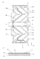
図1(a)は、本発明の実施形態に係る表示パネル用の基板を用いて構築される絵素の構成を模式的に示した平面図であり、図1(b)は、図1(a)のA−A線断面図である。図1に示すように、本発明の実施形態に係る表示パネル用の基板1は、ガラス基板などの透明基板16の表面に、ゲート信号線12および補助容量線15と、第一の絶縁層17と、ソース信号線13およびドレイン14線と、第二の絶縁層18とが、積層して形成される。また、ゲート信号線12に重畳する位置に、位置測定マーク11が浮島状に形成される。一方、対向基板(たとえばカラーフィルタ基板)には、液晶の配向を制御するための凸状の構造物21a〜21eが形成される。ここではこの構造物を、「配向制御構造物」と称する。
FIG. 1A is a plan view schematically showing a configuration of a picture element constructed using a display panel substrate according to an embodiment of the present invention, and FIG. It is AA sectional view taken on the line of a). As shown in FIG. 1, a display panel substrate 1 according to an embodiment of the present invention includes a
ゲート信号線12および補助容量線15は、同じ材料により同じ工程において同一の層に形成される。そしてその表面に絶縁層が形成される。さらにその表面に、ソース信号線13およびドレイン線14が、同じ材料により同じ工程において同一の層に形成される。これにより、ゲート信号線12および補助容量線15のパターンと、ソース信号線13およびドレイン線14のパターンとが、絶縁膜の層を挟んで積層される構成となる。これらのゲート信号線12、補助容量線15、ソース信号線13、ドレイン線14の構成、材質、形成方法などは、従来一般の構成や方法が適用できることから、説明は省略する。
The
位置測定マーク11は、ソース信号線13およびドレイン線14のパターンと、ゲート信号線12のパターンとの相対的な位置を測定するためのパターンである。この位置測定マーク11は、ソース信号線13およびドレイン線14のパターンと同じ層に形成される。そして、ソース信号線13およびドレイン線14のパターンを形成する工程において、同じ材料を用いて同じ工程で形成される。したがって、この位置測定マーク11と、ソース信号線13およびドレイン線14のパターンとの相対的な位置関係は固定されている。
The
この位置測定マーク11は、ゲート信号線12、補助容量線15、ソース信号線13もしくはドレイン線14のいずれとも電気的な接続が構成されない、または電気的な接続が意図されない。別の言い方をすれば、この位置測定マーク11は、前記各線12,13,14,15との関係において、なんらの電気的・電子的な機能を有しない、または機能させることを意図しない。すなわち、薄膜トランジスタの駆動に対して、なんらの寄与や影響を有することを意図していない。
The
この位置測定マーク11は、画像認識を用いてそのエッジを検出でき、かつ検出されたエッジからその位置を算出できる形状に形成される。たとえば、図1に示すような正方形や、その他長方形といった四辺形などが適用できる。四辺形のように、相対向する辺が存在する形状であれば、対向する辺のエッジを検出してそれらの中心を算出できるから、高精度で位置の測定を行える。
The
なお、四辺形に限らず、少なくとも一辺以上の直線部分を含む形状も適用できる。この場合、この位置測定マーク11がY軸方向の位置合わせ精度を測定するためのものであれば、その直線部分が、X軸方向に延伸する形状であることが好ましい。一方、X軸方向の位置合わせ精度の測定に用いるものであれば、その直線部分がY軸方向に延伸するものであることが好ましい。このような形状であれば、この直線部分のエッジを検出することにより、各軸方向の位置の測定を行える。
Note that not only the quadrilateral shape but also a shape including a straight line portion of at least one side is applicable. In this case, if the
次いで、この位置測定マーク11を用いたソース信号線13およびドレイン線14のパターンと、ゲート信号線12のパターンとの位置合わせ精度の測定方法について説明する。ここでは、Y軸方向の位置合わせ精度の測定について記す。
Next, a method for measuring the alignment accuracy between the pattern of the
透明基板16上に、ゲート信号線12および補助容量線15、第一の絶縁層17、ソース信号線13およびドレイン線14、位置測定マーク11、第二の絶縁層18を形成した後、位置測定マーク11が含まれる領域を撮影する。この際、ゲート信号線12のエッジが視野内に収まるようにする。そして、画像認識によって、位置測定マーク11のX軸方向に平行な辺のエッジと、ゲート信号線のX軸方向に平行な辺のエッジを検出する。検出した各辺のエッジから、位置測定マークの中心線の位置と、ゲート信号線の中心線の位置を算出する(なお図1は、位置測定マーク11の中心線とゲート信号線12の中心線とが一致している状態を示しており、A−A線はこの両方に共通の中心線を示す)。そして算出された各中心線から、位置測定マーク11とゲート信号線12とのY軸方向の相対的な位置関係を算出する。これにより、ゲート信号線12のパターンと、ソース信号線13およびドレイン線14のパターンとのY軸方向の位置合わせ精度が測定できる。
After forming the
算出された位置合わせ精度が許容範囲内にあれば、次の工程に進む。相対的な位置が許容範囲を超えてずれている場合には、ソース信号線13およびドレイン線14の形成をやり直す。なお、画像認識の方法、画像認識に用いる装置は、従来一般に用いられる各種方法や各種装置を適用できる。したがって、これらの説明は省略する。
If the calculated alignment accuracy is within the allowable range, the process proceeds to the next step. When the relative position is shifted beyond the allowable range, the
このような位置測定マーク11を用いて位置合わせ精度の測定を行う構成とすれば、ドレイン線14に位置合わせ精度の測定用の直線部分を形成する必要がなくなる。このため、ドレイン線14の設計の自由度が向上する。したがって、ドレイン線14を、そのほぼ全長にわたって対向基板に形成される配向制御構造物21a〜21eのいずれかに重畳させる設計にでき、絵素の開口率の向上が図られる。また、開口率を低下させないためにドレイン線14の幅を細くする必要もなくなるから、プロセスマージンを小さくしなくてもよい。さらに、この位置測定マーク11は、ゲート信号線12に重畳しているから、絵素の開口率を低下させない。また、浮島状に形成されるから、絵素の駆動にも影響を与えることはない。
If the
以上、本発明の実施形態について詳細に説明したが、本発明は、前記実施形態になんら限定されるものではなく、本発明の趣旨を逸脱しない範囲において種々の改変が可能である。 As mentioned above, although embodiment of this invention was described in detail, this invention is not limited to the said embodiment at all, and various modification | change is possible in the range which does not deviate from the meaning of this invention.
前記実施形態においては、位置測定マーク11が正方形に形成される構成を示したが、この形状に限定されるものではない。要は、画像認識を用いてそのエッジを検出でき、かつ検出されたエッジからその位置を算出できる形状に形成されればよい。
In the said embodiment, although the
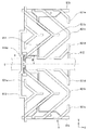
図2は、本発明の実施形態に係る基板の変形例を示す。この図2に示すように、位置測定マーク11’が長方形に形成される構成であってもよい。この位置測定マーク11’をY軸方向の位置合わせ精度の測定に用いるのであれば、X軸に平行な辺の長さが、画像認識を用いて所定の精度でそのエッジを検出できる程度であればよい。一方、Y軸に平行な辺の長さは特に限定されない。したがって、図に示すようなY軸方向に短い長方形のほか、Y軸方向に長い長方形であってもよい。
FIG. 2 shows a modification of the substrate according to the embodiment of the present invention. As shown in FIG. 2, the position measurement mark 11 'may be formed in a rectangular shape. If this
また、三角形やその他の多角形であってもよい。また、直線部分を有する形状に限らず、曲線部分を有する形状であってもよい。たとえば、浮島パターンのエッジに円弧形状が含まれる形状であれば、検出されたエッジから円弧の中心を算出することができる。したがって、円形、半月形、扇形などの形状であってもよい。 Further, it may be a triangle or other polygons. Further, the shape is not limited to a shape having a straight line portion, but may be a shape having a curved line portion. For example, if the arc shape is included in the edge of the floating island pattern, the center of the arc can be calculated from the detected edge. Therefore, it may be a circular shape, a half moon shape, a sector shape, or the like.
位置測定マークが形成される位置は、ゲート信号線との相対的な位置関係を測定できる位置であればよい。たとえば、本実施形態のように、ゲート信号線と補助容量線とが同時に形成される構成であれば(換言すると、ゲート信号線と補助容量線との相対的な位置関係が固定されている構成であれば)、補助容量線に重畳する位置であってもよい。また、必ずしもゲート信号線または補助容量線に重畳する位置である必要はない。たとえば、ゲート信号線または補助容量線の近傍の位置であってもよい。ただし、絵素の開口部を低下させないためには、絵素の領域外であることが好ましい。 The position where the position measurement mark is formed may be a position where the relative positional relationship with the gate signal line can be measured. For example, as in the present embodiment, if the gate signal line and the auxiliary capacitance line are formed at the same time (in other words, the relative positional relationship between the gate signal line and the auxiliary capacitance line is fixed) If so, the position may be superimposed on the auxiliary capacitance line. Further, the position does not necessarily overlap with the gate signal line or the auxiliary capacitance line. For example, it may be a position in the vicinity of the gate signal line or the auxiliary capacitance line. However, in order not to reduce the opening of the picture element, it is preferable to be outside the picture element region.
位置測定マークが形成される層も、ソース信号線およびドレイン線のパターンが形成される層と同じである必要ない。さらに、前記実施形態およびその変形例においては、位置測定マークがゲート信号線に完全に重畳する構成を示したが、必ずしも全体が重畳する構成である必要はなく、一部が重畳する構成であってもよい。 The layer in which the position measurement mark is formed need not be the same as the layer in which the pattern of the source signal line and the drain line is formed. Furthermore, in the above-described embodiment and the modification thereof, the configuration in which the position measurement mark is completely superimposed on the gate signal line is shown. However, the entire configuration is not necessarily superimposed, and a portion is superimposed. May be.
なお、前記実施形態においては、Y軸方向の位置合わせ精度の測定に用いる構成を示したが、X軸方向の位置合わせ精度の測定に用いることもできる。 In the above-described embodiment, the configuration used for measuring the alignment accuracy in the Y-axis direction is shown. However, the configuration can also be used for measuring the alignment accuracy in the X-axis direction.
Claims (4)
Applications Claiming Priority (3)
| Application Number | Priority Date | Filing Date | Title |
|---|---|---|---|
| JP2005275640 | 2005-09-22 | ||
| JP2005275640 | 2005-09-22 | ||
| PCT/JP2006/318331 WO2007034740A1 (en) | 2005-09-22 | 2006-09-15 | Display panel substrate and display panel having the substrate |
Publications (2)
| Publication Number | Publication Date |
|---|---|
| JPWO2007034740A1 JPWO2007034740A1 (en) | 2009-03-26 |
| JP4660552B2 true JP4660552B2 (en) | 2011-03-30 |
Family
ID=37888785
Family Applications (1)
| Application Number | Title | Priority Date | Filing Date |
|---|---|---|---|
| JP2007536469A Expired - Fee Related JP4660552B2 (en) | 2005-09-22 | 2006-09-15 | Display panel substrate and display panel including the substrate |
Country Status (4)
| Country | Link |
|---|---|
| US (3) | US8022559B2 (en) |
| JP (1) | JP4660552B2 (en) |
| CN (1) | CN101268415A (en) |
| WO (1) | WO2007034740A1 (en) |
Families Citing this family (3)
| Publication number | Priority date | Publication date | Assignee | Title |
|---|---|---|---|---|
| CN102646629B (en) * | 2011-07-05 | 2014-04-02 | 北京京东方光电科技有限公司 | Array substrate and manufacturing method thereof |
| CN105511126B (en) * | 2016-01-21 | 2018-11-13 | 京东方科技集团股份有限公司 | Display panel and preparation method thereof and detection method |
| KR102673361B1 (en) * | 2019-08-02 | 2024-06-13 | 삼성디스플레이 주식회사 | Display device |
Citations (2)
| Publication number | Priority date | Publication date | Assignee | Title |
|---|---|---|---|---|
| JPH05323342A (en) * | 1992-05-19 | 1993-12-07 | Casio Comput Co Ltd | Conductive pattern formed panel |
| JP2003302654A (en) * | 2002-04-12 | 2003-10-24 | Hitachi Ltd | Display device |
Family Cites Families (18)
| Publication number | Priority date | Publication date | Assignee | Title |
|---|---|---|---|---|
| JPH04294329A (en) | 1991-03-22 | 1992-10-19 | G T C:Kk | Liquid crystal display device |
| TW543787U (en) * | 1996-03-29 | 2003-07-21 | Toshiba Corp | Liquid crystal display apparatus |
| US6204895B1 (en) * | 1997-09-30 | 2001-03-20 | Kabushiki Kaisha Toshiba | Display panel associated with light collecting plate and position adjusting method using microlenses for the display panel |
| JP3538073B2 (en) * | 1999-07-29 | 2004-06-14 | Nec液晶テクノロジー株式会社 | Active matrix type liquid crystal display device having a color layer on a substrate side on which a TFT is mounted and a method of manufacturing the same |
| JP2001148480A (en) * | 1999-11-18 | 2001-05-29 | Nec Corp | Thin film transistor and device and method for manufacturing the same |
| JP4884586B2 (en) * | 2000-12-18 | 2012-02-29 | 株式会社 日立ディスプレイズ | Liquid crystal display |
| JP2002221735A (en) * | 2001-01-26 | 2002-08-09 | Matsushita Electric Ind Co Ltd | Active matrix substrate, liquid crystal display device, and manufacturing method thereof |
| JP2003058073A (en) * | 2001-08-08 | 2003-02-28 | Seiko Epson Corp | Electro-optical device manufacturing method, electro-optical device, and electronic apparatus |
| KR100801151B1 (en) * | 2001-10-04 | 2008-02-05 | 엘지.필립스 엘시디 주식회사 | Black Matrix for Liquid Crystal Display |
| JP3992976B2 (en) * | 2001-12-21 | 2007-10-17 | 株式会社半導体エネルギー研究所 | Method for manufacturing semiconductor device |
| JP2003209041A (en) * | 2002-01-15 | 2003-07-25 | Seiko Epson Corp | Pattern alignment accuracy measuring method, pattern forming method, manufacturing method of electro-optical device, manufacturing method of semiconductor device |
| TWI310849B (en) * | 2002-02-06 | 2009-06-11 | Au Optronics Corp | Pixel structure |
| JP2004054069A (en) * | 2002-07-23 | 2004-02-19 | Advanced Display Inc | Display device and method for repairing disconnection of display device |
| JP2004304083A (en) * | 2003-03-31 | 2004-10-28 | Seiko Epson Corp | Patterning accuracy measuring method, pattern forming method, thin film transistor manufacturing method, semiconductor device manufacturing method, electro-optical device, and electronic equipment |
| JP2004317728A (en) * | 2003-04-15 | 2004-11-11 | Seiko Epson Corp | Substrate with alignment mark, method of manufacturing the same, substrate for electro-optical device, and electro-optical device |
| JP4522145B2 (en) | 2004-05-25 | 2010-08-11 | シャープ株式会社 | Display device substrate, manufacturing method thereof, and display device |
| TW200638143A (en) * | 2004-10-29 | 2006-11-01 | Toshiba Matsushita Display Tec | Display device |
| KR101140241B1 (en) * | 2005-06-27 | 2012-04-26 | 엘지디스플레이 주식회사 | Liquid crsytal display device using allign mark |
-
2006
- 2006-09-15 CN CNA2006800348352A patent/CN101268415A/en active Pending
- 2006-09-15 US US12/067,518 patent/US8022559B2/en active Active
- 2006-09-15 JP JP2007536469A patent/JP4660552B2/en not_active Expired - Fee Related
- 2006-09-15 WO PCT/JP2006/318331 patent/WO2007034740A1/en not_active Ceased
-
2010
- 2010-12-30 US US12/981,699 patent/US8008789B2/en active Active
-
2011
- 2011-07-14 US US13/182,466 patent/US8193649B2/en active Active
Patent Citations (2)
| Publication number | Priority date | Publication date | Assignee | Title |
|---|---|---|---|---|
| JPH05323342A (en) * | 1992-05-19 | 1993-12-07 | Casio Comput Co Ltd | Conductive pattern formed panel |
| JP2003302654A (en) * | 2002-04-12 | 2003-10-24 | Hitachi Ltd | Display device |
Also Published As
| Publication number | Publication date |
|---|---|
| US8022559B2 (en) | 2011-09-20 |
| JPWO2007034740A1 (en) | 2009-03-26 |
| US8193649B2 (en) | 2012-06-05 |
| US8008789B2 (en) | 2011-08-30 |
| WO2007034740A1 (en) | 2007-03-29 |
| US20090236760A1 (en) | 2009-09-24 |
| US20110267569A1 (en) | 2011-11-03 |
| CN101268415A (en) | 2008-09-17 |
| US20110096284A1 (en) | 2011-04-28 |
Similar Documents
| Publication | Publication Date | Title |
|---|---|---|
| JP4869789B2 (en) | Display device | |
| JP4600463B2 (en) | Liquid crystal display | |
| US11841590B2 (en) | Display device | |
| JP5448940B2 (en) | Liquid crystal display | |
| US12025898B2 (en) | Display device | |
| US10520761B2 (en) | Method of producing substrate having alignment mark | |
| WO2017119338A1 (en) | Display device | |
| JP4660552B2 (en) | Display panel substrate and display panel including the substrate | |
| CN109754764B (en) | display device | |
| JP2022132583A (en) | detector | |
| CN111722447A (en) | display device | |
| KR101183409B1 (en) | Active matrix substrate, display panel and display device | |
| JP5403539B2 (en) | Horizontal electric field type liquid crystal display device | |
| JP4609483B2 (en) | Liquid crystal display device | |
| JP2009003381A (en) | Electrode connection structure and liquid crystal display unit | |
| US10330994B2 (en) | Active matrix substrate, liquid crystal panel, and method for manufacturing active matrix substrate | |
| JP2007093859A (en) | Liquid crystal device and electronic apparatus | |
| JP2006276747A (en) | Pattern forming method and manufacturing method of liquid crystal display device | |
| CN116027598A (en) | Active matrix substrate and display device | |
| TW201913194A (en) | Active device substrate |
Legal Events
| Date | Code | Title | Description |
|---|---|---|---|
| A131 | Notification of reasons for refusal |
Free format text: JAPANESE INTERMEDIATE CODE: A131 Effective date: 20100921 |
|
| A521 | Request for written amendment filed |
Free format text: JAPANESE INTERMEDIATE CODE: A523 Effective date: 20101112 |
|
| TRDD | Decision of grant or rejection written | ||
| A01 | Written decision to grant a patent or to grant a registration (utility model) |
Free format text: JAPANESE INTERMEDIATE CODE: A01 Effective date: 20101207 |
|
| A01 | Written decision to grant a patent or to grant a registration (utility model) |
Free format text: JAPANESE INTERMEDIATE CODE: A01 |
|
| A61 | First payment of annual fees (during grant procedure) |
Free format text: JAPANESE INTERMEDIATE CODE: A61 Effective date: 20101228 |
|
| FPAY | Renewal fee payment (event date is renewal date of database) |
Free format text: PAYMENT UNTIL: 20140107 Year of fee payment: 3 |
|
| R150 | Certificate of patent or registration of utility model |
Ref document number: 4660552 Country of ref document: JP Free format text: JAPANESE INTERMEDIATE CODE: R150 Free format text: JAPANESE INTERMEDIATE CODE: R150 |
|
| LAPS | Cancellation because of no payment of annual fees |