JP4639352B2 - 波長≦100nmで物体を検査する検査系 - Google Patents
波長≦100nmで物体を検査する検査系 Download PDFInfo
- Publication number
- JP4639352B2 JP4639352B2 JP2004504243A JP2004504243A JP4639352B2 JP 4639352 B2 JP4639352 B2 JP 4639352B2 JP 2004504243 A JP2004504243 A JP 2004504243A JP 2004504243 A JP2004504243 A JP 2004504243A JP 4639352 B2 JP4639352 B2 JP 4639352B2
- Authority
- JP
- Japan
- Prior art keywords
- mirror
- plane
- image
- mask
- imaging
- Prior art date
- Legal status (The legal status is an assumption and is not a legal conclusion. Google has not performed a legal analysis and makes no representation as to the accuracy of the status listed.)
- Expired - Lifetime
Links
- 238000007689 inspection Methods 0.000 title claims abstract description 77
- 230000003287 optical effect Effects 0.000 claims abstract description 80
- 238000003384 imaging method Methods 0.000 claims description 67
- 238000005286 illumination Methods 0.000 claims description 41
- 238000001393 microlithography Methods 0.000 abstract description 11
- 238000000034 method Methods 0.000 abstract description 9
- 230000007547 defect Effects 0.000 description 25
- 238000005259 measurement Methods 0.000 description 25
- 230000008439 repair process Effects 0.000 description 11
- 238000004458 analytical method Methods 0.000 description 8
- 238000004519 manufacturing process Methods 0.000 description 7
- 230000008569 process Effects 0.000 description 7
- 210000001747 pupil Anatomy 0.000 description 7
- OAICVXFJPJFONN-UHFFFAOYSA-N Phosphorus Chemical compound [P] OAICVXFJPJFONN-UHFFFAOYSA-N 0.000 description 4
- 238000001900 extreme ultraviolet lithography Methods 0.000 description 4
- 238000004088 simulation Methods 0.000 description 4
- 239000000758 substrate Substances 0.000 description 4
- 230000008859 change Effects 0.000 description 3
- 230000000875 corresponding effect Effects 0.000 description 3
- 238000011156 evaluation Methods 0.000 description 3
- 230000004907 flux Effects 0.000 description 3
- 238000012634 optical imaging Methods 0.000 description 3
- 238000012545 processing Methods 0.000 description 3
- 230000008901 benefit Effects 0.000 description 2
- 230000005540 biological transmission Effects 0.000 description 2
- 238000004364 calculation method Methods 0.000 description 2
- 239000000463 material Substances 0.000 description 2
- 238000000206 photolithography Methods 0.000 description 2
- 238000002360 preparation method Methods 0.000 description 2
- 238000003908 quality control method Methods 0.000 description 2
- 230000009467 reduction Effects 0.000 description 2
- 238000012360 testing method Methods 0.000 description 2
- 238000001015 X-ray lithography Methods 0.000 description 1
- 230000032683 aging Effects 0.000 description 1
- 230000003321 amplification Effects 0.000 description 1
- 230000015572 biosynthetic process Effects 0.000 description 1
- 239000000969 carrier Substances 0.000 description 1
- 238000012512 characterization method Methods 0.000 description 1
- 238000004140 cleaning Methods 0.000 description 1
- 230000002596 correlated effect Effects 0.000 description 1
- 230000008878 coupling Effects 0.000 description 1
- 238000010168 coupling process Methods 0.000 description 1
- 238000005859 coupling reaction Methods 0.000 description 1
- 238000013461 design Methods 0.000 description 1
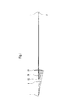
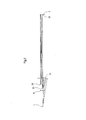
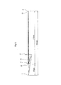
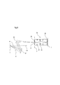
- 238000010586 diagram Methods 0.000 description 1
- 230000000694 effects Effects 0.000 description 1
- 230000005684 electric field Effects 0.000 description 1
- 238000005516 engineering process Methods 0.000 description 1
- 238000007730 finishing process Methods 0.000 description 1
- 239000011521 glass Substances 0.000 description 1
- 150000002500 ions Chemical class 0.000 description 1
- 238000004377 microelectronic Methods 0.000 description 1
- 238000003199 nucleic acid amplification method Methods 0.000 description 1
- 238000005457 optimization Methods 0.000 description 1
- 238000002047 photoemission electron microscopy Methods 0.000 description 1
- 230000005855 radiation Effects 0.000 description 1
- 230000003595 spectral effect Effects 0.000 description 1
- 238000001228 spectrum Methods 0.000 description 1
- 238000003860 storage Methods 0.000 description 1
- 230000009897 systematic effect Effects 0.000 description 1
- 230000000007 visual effect Effects 0.000 description 1
- 238000003963 x-ray microscopy Methods 0.000 description 1
Images


Classifications
-
- G—PHYSICS
- G21—NUCLEAR PHYSICS; NUCLEAR ENGINEERING
- G21K—TECHNIQUES FOR HANDLING PARTICLES OR IONISING RADIATION NOT OTHERWISE PROVIDED FOR; IRRADIATION DEVICES; GAMMA RAY OR X-RAY MICROSCOPES
- G21K7/00—Gamma- or X-ray microscopes
-
- B—PERFORMING OPERATIONS; TRANSPORTING
- B82—NANOTECHNOLOGY
- B82Y—SPECIFIC USES OR APPLICATIONS OF NANOSTRUCTURES; MEASUREMENT OR ANALYSIS OF NANOSTRUCTURES; MANUFACTURE OR TREATMENT OF NANOSTRUCTURES
- B82Y10/00—Nanotechnology for information processing, storage or transmission, e.g. quantum computing or single electron logic
-
- G—PHYSICS
- G21—NUCLEAR PHYSICS; NUCLEAR ENGINEERING
- G21K—TECHNIQUES FOR HANDLING PARTICLES OR IONISING RADIATION NOT OTHERWISE PROVIDED FOR; IRRADIATION DEVICES; GAMMA RAY OR X-RAY MICROSCOPES
- G21K1/00—Arrangements for handling particles or ionising radiation, e.g. focusing or moderating
- G21K1/06—Arrangements for handling particles or ionising radiation, e.g. focusing or moderating using diffraction, refraction or reflection, e.g. monochromators
- G21K1/062—Devices having a multilayer structure
Landscapes
- Engineering & Computer Science (AREA)
- Physics & Mathematics (AREA)
- High Energy & Nuclear Physics (AREA)
- Chemical & Material Sciences (AREA)
- Nanotechnology (AREA)
- General Engineering & Computer Science (AREA)
- Theoretical Computer Science (AREA)
- Crystallography & Structural Chemistry (AREA)
- Spectroscopy & Molecular Physics (AREA)
- Mathematical Physics (AREA)
- Analysing Materials By The Use Of Radiation (AREA)
- Lenses (AREA)
- Exposure Of Semiconductors, Excluding Electron Or Ion Beam Exposure (AREA)
- Investigating Or Analysing Materials By Optical Means (AREA)
Applications Claiming Priority (3)
| Application Number | Priority Date | Filing Date | Title |
|---|---|---|---|
| DE10220816A DE10220816A1 (de) | 2002-05-10 | 2002-05-10 | Reflektives Röntgenmikroskop und Inspektionssystem zur Untersuchung von Objekten mit Wellenlängen 100 nm |
| DE10220815A DE10220815A1 (de) | 2002-05-10 | 2002-05-10 | Reflektives Röntgenmikroskop und Inspektionssystem zur Untersuchung von Objekten mit Wellenlängen 100 nm |
| PCT/EP2003/004803 WO2003096356A2 (de) | 2002-05-10 | 2003-05-08 | Reflektives röntgenmikroskop und inspektionssystem zur untersuchung von objekten mit wellenlängen ≤ 100nm |
Related Child Applications (1)
| Application Number | Title | Priority Date | Filing Date |
|---|---|---|---|
| JP2009255986A Division JP2010032542A (ja) | 2002-05-10 | 2009-11-09 | 波長≦100nmで物体を検査する反射型X線顕微鏡および検査系 |
Publications (2)
| Publication Number | Publication Date |
|---|---|
| JP2005525565A JP2005525565A (ja) | 2005-08-25 |
| JP4639352B2 true JP4639352B2 (ja) | 2011-02-23 |
Family
ID=29421498
Family Applications (2)
| Application Number | Title | Priority Date | Filing Date |
|---|---|---|---|
| JP2004504243A Expired - Lifetime JP4639352B2 (ja) | 2002-05-10 | 2003-05-08 | 波長≦100nmで物体を検査する検査系 |
| JP2009255986A Pending JP2010032542A (ja) | 2002-05-10 | 2009-11-09 | 波長≦100nmで物体を検査する反射型X線顕微鏡および検査系 |
Family Applications After (1)
| Application Number | Title | Priority Date | Filing Date |
|---|---|---|---|
| JP2009255986A Pending JP2010032542A (ja) | 2002-05-10 | 2009-11-09 | 波長≦100nmで物体を検査する反射型X線顕微鏡および検査系 |
Country Status (7)
| Country | Link |
|---|---|
| US (1) | US7623620B2 (enExample) |
| EP (2) | EP1446813B1 (enExample) |
| JP (2) | JP4639352B2 (enExample) |
| AT (1) | ATE488013T1 (enExample) |
| AU (1) | AU2003268097A1 (enExample) |
| DE (1) | DE50313254D1 (enExample) |
| WO (1) | WO2003096356A2 (enExample) |
Families Citing this family (31)
| Publication number | Priority date | Publication date | Assignee | Title |
|---|---|---|---|---|
| US7351980B2 (en) * | 2005-03-31 | 2008-04-01 | Kla-Tencor Technologies Corp. | All-reflective optical systems for broadband wafer inspection |
| WO2007020004A1 (de) * | 2005-08-17 | 2007-02-22 | Carl Zeiss Smt Ag | Projektionsobjektiv und verfahren zur optimierung einer systemblende eines projektionsobjektivs |
| US7564564B2 (en) * | 2006-08-22 | 2009-07-21 | Artium Technologies, Inc. | Automatic set-up for instrument functions |
| DE102006044202A1 (de) * | 2006-09-15 | 2008-05-21 | Fahrzeugwerk Bernard Krone Gmbh | Dolly-Achse |
| US20080144167A1 (en) * | 2006-12-13 | 2008-06-19 | General Electric Company | Optical imaging system and method for high speed and high resolution |
| DE102007062198A1 (de) | 2007-12-21 | 2009-06-25 | Carl Zeiss Microimaging Gmbh | Katoptrisches Objektiv zur Abbildung eines im Wesentlichen linienförmigen Objektes |
| DE102008015996A1 (de) * | 2008-03-27 | 2009-10-01 | Carl Zeiss Sms Gmbh | Mikroskop und Mikroskopierverfahren zur Untersuchung eines reflektierenden Objektes |
| KR101535230B1 (ko) * | 2009-06-03 | 2015-07-09 | 삼성전자주식회사 | Euv 마스크용 공간 영상 측정 장치 및 방법 |
| WO2010148293A2 (en) | 2009-06-19 | 2010-12-23 | Kla-Tencor Corporation | Euv high throughput inspection system for defect detection on patterned euv masks, mask blanks, and wafers |
| SG176552A1 (en) * | 2009-06-19 | 2012-01-30 | Kla Tencor Tech Corp | Inspection systems and methods for detecting defects on extreme ultraviolet mask blanks |
| NL2004949A (en) * | 2009-08-21 | 2011-02-22 | Asml Netherlands Bv | Inspection method and apparatus. |
| DE102010009022B4 (de) | 2010-02-22 | 2019-10-24 | Carl Zeiss Smt Gmbh | Beleuchtungssystem sowie Projektionsobjektiv einer Maskeninspektionsanlage |
| DE102010029049B4 (de) | 2010-05-18 | 2014-03-13 | Carl Zeiss Smt Gmbh | Beleuchtungsoptik für ein Metrologiesystem für die Untersuchung eines Objekts mit EUV-Beleuchtungslicht sowie Metrologiesystem mit einer derartigen Beleuchtungsoptik |
| DE102010025033B4 (de) * | 2010-06-23 | 2021-02-11 | Carl Zeiss Smt Gmbh | Verfahren zur Defekterkennung und Reparatur von EUV-Masken |
| DE102010047050B4 (de) * | 2010-09-29 | 2021-09-16 | Carl Zeiss Smt Gmbh | Verfahren zur Charakterisierung einer Struktur auf einer Maske und Vorrichtung zur Durchführung des Verfahrens |
| US8837041B2 (en) * | 2010-11-23 | 2014-09-16 | Carl Zeiss Smt Gmbh | Magnifying imaging optical system and metrology system with an imaging optical system of this type |
| JP4761588B1 (ja) * | 2010-12-01 | 2011-08-31 | レーザーテック株式会社 | Euvマスク検査装置 |
| WO2012096847A2 (en) | 2011-01-11 | 2012-07-19 | Kla-Tencor Corporation | Apparatus for euv imaging and methods of using same |
| DE102011003302A1 (de) | 2011-01-28 | 2012-08-02 | Carl Zeiss Smt Gmbh | Vergrößerte abbildende Optik sowie Metrologiesystem mit einer derartigen abbildenden Optik |
| DE102011005881A1 (de) | 2011-03-22 | 2012-05-03 | Carl Zeiss Smt Gmbh | Verfahren zur Einstellung eines Beleuchtungssystems einer Projektionsbelichtungsanlage für die Projektionslithographie |
| DE102011079382B4 (de) * | 2011-07-19 | 2020-11-12 | Carl Zeiss Smt Gmbh | Verfahren und Vorrichtung zum Analysieren und zum Beseitigen eines Defekts einer EUV Maske |
| DE102013204445A1 (de) * | 2013-03-14 | 2014-09-18 | Carl Zeiss Smt Gmbh | Vergrößernde abbildende Optik sowie EUV-Maskeninspektionssystem mit einer derartigen abbildenden Optik |
| DE102013212613B4 (de) | 2013-06-28 | 2015-07-23 | Carl Zeiss Sms Gmbh | Beleuchtungsoptik für ein Metrologiesystem sowie Metrologiesystem mit einer derartigen Beleuchtungsoptik |
| DE102014219755A1 (de) | 2013-10-30 | 2015-04-30 | Carl Zeiss Smt Gmbh | Reflektives optisches Element |
| WO2015124386A1 (en) * | 2014-02-21 | 2015-08-27 | Paul Scherrer Institut | An imaging system in reflection mode using coherent diffraction imaging methods and using micro-pinhole and aperture system |
| EP3518041A1 (en) * | 2018-01-30 | 2019-07-31 | ASML Netherlands B.V. | Inspection apparatus and inspection method |
| JP2020173296A (ja) * | 2019-04-08 | 2020-10-22 | 株式会社ニューフレアテクノロジー | Euvマスクのパターン検査装置及びeuvマスクのパターン検査方法 |
| CN113994485A (zh) * | 2019-05-10 | 2022-01-28 | 日亚化学工业株式会社 | 图像显示装置的制造方法以及图像显示装置 |
| DE102023204172A1 (de) * | 2023-05-05 | 2024-11-07 | Carl Zeiss Smt Gmbh | Optisches System für ein Metrologiesystem sowie Metrologiesystem mit einem derartigen optischen System |
| DE102023129681A1 (de) * | 2023-10-27 | 2025-04-30 | Carl Zeiss Smt Gmbh | Verfahren und Steuervorrichtung zum Analysieren eines Bildes eines Rohlings einer Photomaske für die Mikrolithographie |
| DE102024203890A1 (de) | 2024-04-25 | 2025-10-30 | Carl Zeiss Smt Gmbh | Verfahren zur hochgenauen Lagebestimmung einer Struktur |
Family Cites Families (25)
| Publication number | Priority date | Publication date | Assignee | Title |
|---|---|---|---|---|
| JPS612124A (ja) | 1984-06-14 | 1986-01-08 | Canon Inc | 結像光学系 |
| JP2603225B2 (ja) * | 1986-07-11 | 1997-04-23 | キヤノン株式会社 | X線投影露光装置及び半導体製造方法 |
| EP0947882B1 (en) * | 1986-07-11 | 2006-03-29 | Canon Kabushiki Kaisha | X-ray reduction projection exposure system of reflection type |
| US4912737A (en) | 1987-10-30 | 1990-03-27 | Hamamatsu Photonics K.K. | X-ray image observing device |
| JPH02210299A (ja) | 1989-02-10 | 1990-08-21 | Olympus Optical Co Ltd | X線用光学系及びそれに用いる多層膜反射鏡 |
| JPH0782117B2 (ja) * | 1989-02-23 | 1995-09-06 | オリンパス光学工業株式会社 | 反射型結像光学系 |
| JP2865257B2 (ja) | 1989-03-07 | 1999-03-08 | オリンパス光学工業株式会社 | シュヴアルツシルド光学系 |
| US5063586A (en) | 1989-10-13 | 1991-11-05 | At&T Bell Laboratories | Apparatus for semiconductor lithography |
| JP2945431B2 (ja) | 1990-03-01 | 1999-09-06 | オリンパス光学工業株式会社 | 結像型x線顕微鏡 |
| JP2921038B2 (ja) | 1990-06-01 | 1999-07-19 | キヤノン株式会社 | X線を用いた観察装置 |
| DE4027285A1 (de) | 1990-08-29 | 1992-03-05 | Zeiss Carl Fa | Roentgenmikroskop |
| US5291339A (en) | 1990-11-30 | 1994-03-01 | Olympus Optical Co., Ltd. | Schwarzschild optical system |
| JPH04321047A (ja) | 1991-01-21 | 1992-11-11 | Nikon Corp | フォトマスク検査装置及びフォトマスク検査方法 |
| JPH04353800A (ja) * | 1991-05-31 | 1992-12-08 | Olympus Optical Co Ltd | 軟x線顕微鏡 |
| US5177774A (en) * | 1991-08-23 | 1993-01-05 | Trustees Of Princeton University | Reflection soft X-ray microscope and method |
| JPH06237016A (ja) * | 1993-02-09 | 1994-08-23 | Matsushita Electric Ind Co Ltd | 光ファイバモジュールおよびその製造方法 |
| JPH0728226A (ja) | 1993-04-30 | 1995-01-31 | Internatl Business Mach Corp <Ibm> | 領域的イメージを測定する装置及び方法 |
| JP3336361B2 (ja) * | 1993-06-11 | 2002-10-21 | 株式会社ニコン | 縮小投影露光用反射型x線マスクの検査装置および検査方法 |
| US6438199B1 (en) | 1998-05-05 | 2002-08-20 | Carl-Zeiss-Stiftung | Illumination system particularly for microlithography |
| DE19923609A1 (de) * | 1998-05-30 | 1999-12-02 | Zeiss Carl Fa | Ringfeld-4-Spiegelsysteme mit konvexem Primärspiegel für die EUV-Lithographie |
| US6328482B1 (en) * | 1998-06-08 | 2001-12-11 | Benjamin Bin Jian | Multilayer optical fiber coupler |
| JP4374735B2 (ja) * | 1999-08-11 | 2009-12-02 | 株式会社ニコン | 反射型軟x線顕微鏡、マスク検査装置及び反射マスクの製造方法 |
| EP1126477A3 (de) * | 2000-02-14 | 2003-06-18 | Leica Microsystems Lithography GmbH | Verfahren zur Untersuchung von Strukturen auf einem Halbleiter-Substrat |
| JP2002329473A (ja) * | 2001-02-27 | 2002-11-15 | Jeol Ltd | X線分光器を備えた透過型電子顕微鏡 |
| DE10319269A1 (de) * | 2003-04-25 | 2004-11-25 | Carl Zeiss Sms Gmbh | Abbildungssystem für ein, auf extrem ultravioletter (EUV) Strahlung basierendem Mikroskop |
-
2003
- 2003-05-08 DE DE50313254T patent/DE50313254D1/de not_active Expired - Lifetime
- 2003-05-08 EP EP03740130A patent/EP1446813B1/de not_active Expired - Lifetime
- 2003-05-08 JP JP2004504243A patent/JP4639352B2/ja not_active Expired - Lifetime
- 2003-05-08 AT AT03740130T patent/ATE488013T1/de active
- 2003-05-08 AU AU2003268097A patent/AU2003268097A1/en not_active Abandoned
- 2003-05-08 WO PCT/EP2003/004803 patent/WO2003096356A2/de not_active Ceased
- 2003-05-08 EP EP04013866.1A patent/EP1455365A3/de not_active Withdrawn
-
2004
- 2004-11-08 US US10/983,362 patent/US7623620B2/en not_active Expired - Lifetime
-
2009
- 2009-11-09 JP JP2009255986A patent/JP2010032542A/ja active Pending
Also Published As
| Publication number | Publication date |
|---|---|
| JP2010032542A (ja) | 2010-02-12 |
| ATE488013T1 (de) | 2010-11-15 |
| US7623620B2 (en) | 2009-11-24 |
| EP1446813A2 (de) | 2004-08-18 |
| WO2003096356A2 (de) | 2003-11-20 |
| DE50313254D1 (de) | 2010-12-23 |
| AU2003268097A1 (en) | 2003-11-11 |
| EP1455365A3 (de) | 2014-12-17 |
| JP2005525565A (ja) | 2005-08-25 |
| US20050201514A1 (en) | 2005-09-15 |
| AU2003268097A8 (en) | 2003-11-11 |
| EP1455365A2 (de) | 2004-09-08 |
| WO2003096356A3 (de) | 2004-05-21 |
| EP1446813B1 (de) | 2010-11-10 |
Similar Documents
| Publication | Publication Date | Title |
|---|---|---|
| JP4639352B2 (ja) | 波長≦100nmで物体を検査する検査系 | |
| JP6132319B2 (ja) | 結像光学系 | |
| JP6470188B2 (ja) | 拡大結像光学ユニット及びそのような結像光学ユニットを有するeuvマスク検査系 | |
| US20040057107A1 (en) | Reflective lithography mask inspection tool based on achromatic fresnel optics | |
| US20130063716A1 (en) | Illumination optics for a metrology system for examining an object using euv illumination light and metrology system comprising an illumination optics of this type | |
| JP5643755B2 (ja) | 結像光学系 | |
| JP3996135B2 (ja) | リソグラフィー装置およびデバイス製造方法 | |
| JPH10177139A (ja) | 反射屈折両特性原理を用いた広帯域紫外線画像システム | |
| DE10220815A1 (de) | Reflektives Röntgenmikroskop und Inspektionssystem zur Untersuchung von Objekten mit Wellenlängen 100 nm | |
| JP2008176326A (ja) | 結像光学系 | |
| DE10220816A1 (de) | Reflektives Röntgenmikroskop und Inspektionssystem zur Untersuchung von Objekten mit Wellenlängen 100 nm | |
| EP3762781B1 (en) | Arbitrary wavefront compensator for deep-ultraviolet (duv) optical imaging system | |
| JP5686901B2 (ja) | 投影露光システム及び投影露光方法 | |
| JP2006332586A (ja) | 測定装置、露光装置及び方法、並びに、デバイス製造方法 | |
| JP2024059661A (ja) | 計測光に関する物体の反射率を計測するための方法およびその方法を実行するための計量システム | |
| TWI443474B (zh) | 光學系統、包含此類型光學系統之用於微蝕刻的投影曝光裝置、以及以此類型投影曝光裝置製造微結構組件之方法 | |
| KR100756139B1 (ko) | 노광장치 및 그것을 이용한 디바이스의 제조방법 | |
| Goldberg et al. | Actinic extreme ultraviolet mask inspection beyond 0.25 numericalaperture | |
| US6894837B2 (en) | Imaging system for an extreme ultraviolet (EUV) beam-based microscope | |
| Juschkin et al. | Two magnification steps EUV microscopy with a Schwarzschild objective and an adapted zone plate lens | |
| TWI912074B (zh) | 用於測量系統以檢查物體的放大成像光學單元 | |
| US20070070502A1 (en) | Illuminating and imaging system comprising a diffractive beam splitter | |
| JP2024534800A (ja) | X線照射された物体を結像する(image)結像光学機構 | |
| JP2024170372A (ja) | 計測システム用の光学系、およびそのような光学系を備える計測システム | |
| JP2003279341A (ja) | 測定方法、投影光学系の調整方法、露光装置の調整方法、露光装置、及びデバイス製造方法 |
Legal Events
| Date | Code | Title | Description |
|---|---|---|---|
| A521 | Request for written amendment filed |
Free format text: JAPANESE INTERMEDIATE CODE: A523 Effective date: 20041202 |
|
| A621 | Written request for application examination |
Free format text: JAPANESE INTERMEDIATE CODE: A621 Effective date: 20051125 |
|
| A131 | Notification of reasons for refusal |
Free format text: JAPANESE INTERMEDIATE CODE: A131 Effective date: 20080709 |
|
| A601 | Written request for extension of time |
Free format text: JAPANESE INTERMEDIATE CODE: A601 Effective date: 20081009 |
|
| A602 | Written permission of extension of time |
Free format text: JAPANESE INTERMEDIATE CODE: A602 Effective date: 20081023 |
|
| A601 | Written request for extension of time |
Free format text: JAPANESE INTERMEDIATE CODE: A601 Effective date: 20081110 |
|
| A602 | Written permission of extension of time |
Free format text: JAPANESE INTERMEDIATE CODE: A602 Effective date: 20081119 |
|
| A601 | Written request for extension of time |
Free format text: JAPANESE INTERMEDIATE CODE: A601 Effective date: 20081209 |
|
| A521 | Request for written amendment filed |
Free format text: JAPANESE INTERMEDIATE CODE: A523 Effective date: 20090105 |
|
| A602 | Written permission of extension of time |
Free format text: JAPANESE INTERMEDIATE CODE: A602 Effective date: 20090106 |
|
| A131 | Notification of reasons for refusal |
Free format text: JAPANESE INTERMEDIATE CODE: A131 Effective date: 20090507 |
|
| A601 | Written request for extension of time |
Free format text: JAPANESE INTERMEDIATE CODE: A601 Effective date: 20090731 |
|
| A602 | Written permission of extension of time |
Free format text: JAPANESE INTERMEDIATE CODE: A602 Effective date: 20090807 |
|
| A601 | Written request for extension of time |
Free format text: JAPANESE INTERMEDIATE CODE: A601 Effective date: 20090907 |
|
| A602 | Written permission of extension of time |
Free format text: JAPANESE INTERMEDIATE CODE: A602 Effective date: 20090924 |
|
| RD02 | Notification of acceptance of power of attorney |
Free format text: JAPANESE INTERMEDIATE CODE: A7422 Effective date: 20091008 |
|
| RD03 | Notification of appointment of power of attorney |
Free format text: JAPANESE INTERMEDIATE CODE: A7423 Effective date: 20091008 |
|
| A521 | Request for written amendment filed |
Free format text: JAPANESE INTERMEDIATE CODE: A523 Effective date: 20091109 |
|
| A131 | Notification of reasons for refusal |
Free format text: JAPANESE INTERMEDIATE CODE: A131 Effective date: 20100531 |
|
| A521 | Request for written amendment filed |
Free format text: JAPANESE INTERMEDIATE CODE: A523 Effective date: 20100830 |
|
| TRDD | Decision of grant or rejection written | ||
| A01 | Written decision to grant a patent or to grant a registration (utility model) |
Free format text: JAPANESE INTERMEDIATE CODE: A01 Effective date: 20101012 |
|
| A01 | Written decision to grant a patent or to grant a registration (utility model) |
Free format text: JAPANESE INTERMEDIATE CODE: A01 |
|
| A61 | First payment of annual fees (during grant procedure) |
Free format text: JAPANESE INTERMEDIATE CODE: A61 Effective date: 20101108 |
|
| R150 | Certificate of patent or registration of utility model |
Free format text: JAPANESE INTERMEDIATE CODE: R150 Ref document number: 4639352 Country of ref document: JP Free format text: JAPANESE INTERMEDIATE CODE: R150 |
|
| FPAY | Renewal fee payment (event date is renewal date of database) |
Free format text: PAYMENT UNTIL: 20131210 Year of fee payment: 3 |
|
| R250 | Receipt of annual fees |
Free format text: JAPANESE INTERMEDIATE CODE: R250 |
|
| R250 | Receipt of annual fees |
Free format text: JAPANESE INTERMEDIATE CODE: R250 |
|
| R250 | Receipt of annual fees |
Free format text: JAPANESE INTERMEDIATE CODE: R250 |
|
| R250 | Receipt of annual fees |
Free format text: JAPANESE INTERMEDIATE CODE: R250 |
|
| S111 | Request for change of ownership or part of ownership |
Free format text: JAPANESE INTERMEDIATE CODE: R313115 |
|
| S631 | Written request for registration of reclamation of domicile |
Free format text: JAPANESE INTERMEDIATE CODE: R313631 |
|
| R350 | Written notification of registration of transfer |
Free format text: JAPANESE INTERMEDIATE CODE: R350 |
|
| R250 | Receipt of annual fees |
Free format text: JAPANESE INTERMEDIATE CODE: R250 |
|
| R250 | Receipt of annual fees |
Free format text: JAPANESE INTERMEDIATE CODE: R250 |
|
| R250 | Receipt of annual fees |
Free format text: JAPANESE INTERMEDIATE CODE: R250 |
|
| R250 | Receipt of annual fees |
Free format text: JAPANESE INTERMEDIATE CODE: R250 |
|
| R250 | Receipt of annual fees |
Free format text: JAPANESE INTERMEDIATE CODE: R250 |
|
| R250 | Receipt of annual fees |
Free format text: JAPANESE INTERMEDIATE CODE: R250 |
|
| EXPY | Cancellation because of completion of term |