JP4606103B2 - 液晶表示装置 - Google Patents
液晶表示装置 Download PDFInfo
- Publication number
- JP4606103B2 JP4606103B2 JP2004274993A JP2004274993A JP4606103B2 JP 4606103 B2 JP4606103 B2 JP 4606103B2 JP 2004274993 A JP2004274993 A JP 2004274993A JP 2004274993 A JP2004274993 A JP 2004274993A JP 4606103 B2 JP4606103 B2 JP 4606103B2
- Authority
- JP
- Japan
- Prior art keywords
- pixel
- electrode
- liquid crystal
- pixel electrode
- signal line
- Prior art date
- Legal status (The legal status is an assumption and is not a legal conclusion. Google has not performed a legal analysis and makes no representation as to the accuracy of the status listed.)
- Active
Links
- 239000004973 liquid crystal related substance Substances 0.000 title claims description 56
- 239000010408 film Substances 0.000 claims description 40
- 239000010409 thin film Substances 0.000 claims description 32
- 239000004065 semiconductor Substances 0.000 claims description 19
- 239000000758 substrate Substances 0.000 claims description 15
- 239000004020 conductor Substances 0.000 claims description 9
- 244000126211 Hericium coralloides Species 0.000 claims 1
- 101100489584 Solanum lycopersicum TFT1 gene Proteins 0.000 description 21
- 239000010410 layer Substances 0.000 description 20
- 101100214488 Solanum lycopersicum TFT2 gene Proteins 0.000 description 19
- 230000001681 protective effect Effects 0.000 description 13
- 101100309712 Arabidopsis thaliana SD11 gene Proteins 0.000 description 12
- 230000005684 electric field Effects 0.000 description 12
- 101100309717 Arabidopsis thaliana SD22 gene Proteins 0.000 description 11
- 102100036464 Activated RNA polymerase II transcriptional coactivator p15 Human genes 0.000 description 5
- 101000713904 Homo sapiens Activated RNA polymerase II transcriptional coactivator p15 Proteins 0.000 description 5
- 229910004444 SUB1 Inorganic materials 0.000 description 5
- 230000000694 effects Effects 0.000 description 5
- 230000015572 biosynthetic process Effects 0.000 description 3
- 230000008859 change Effects 0.000 description 3
- 230000007547 defect Effects 0.000 description 3
- 238000010586 diagram Methods 0.000 description 3
- 239000000463 material Substances 0.000 description 3
- 229910010272 inorganic material Inorganic materials 0.000 description 2
- 239000011147 inorganic material Substances 0.000 description 2
- 238000004519 manufacturing process Methods 0.000 description 2
- 239000011159 matrix material Substances 0.000 description 2
- 238000000034 method Methods 0.000 description 2
- 239000011368 organic material Substances 0.000 description 2
- 229910004438 SUB2 Inorganic materials 0.000 description 1
- 101100311330 Schizosaccharomyces pombe (strain 972 / ATCC 24843) uap56 gene Proteins 0.000 description 1
- 239000003086 colorant Substances 0.000 description 1
- 230000001771 impaired effect Effects 0.000 description 1
- AMGQUBHHOARCQH-UHFFFAOYSA-N indium;oxotin Chemical compound [In].[Sn]=O AMGQUBHHOARCQH-UHFFFAOYSA-N 0.000 description 1
- 239000011229 interlayer Substances 0.000 description 1
- OSDXSOSJRPQCHJ-XVNBXDOJSA-N methyl 3-(3,4-dihydroxyphenyl)-3-[(E)-3-(3,4-dihydroxyphenyl)prop-2-enoyl]oxypropanoate Chemical compound C=1C=C(O)C(O)=CC=1C(CC(=O)OC)OC(=O)\C=C\C1=CC=C(O)C(O)=C1 OSDXSOSJRPQCHJ-XVNBXDOJSA-N 0.000 description 1
- 230000004048 modification Effects 0.000 description 1
- 238000012986 modification Methods 0.000 description 1
- 230000002093 peripheral effect Effects 0.000 description 1
- 230000008569 process Effects 0.000 description 1
- 230000009467 reduction Effects 0.000 description 1
- 101150018444 sub2 gene Proteins 0.000 description 1
- 239000000126 substance Substances 0.000 description 1
Images


Classifications
-
- G—PHYSICS
- G02—OPTICS
- G02F—OPTICAL DEVICES OR ARRANGEMENTS FOR THE CONTROL OF LIGHT BY MODIFICATION OF THE OPTICAL PROPERTIES OF THE MEDIA OF THE ELEMENTS INVOLVED THEREIN; NON-LINEAR OPTICS; FREQUENCY-CHANGING OF LIGHT; OPTICAL LOGIC ELEMENTS; OPTICAL ANALOGUE/DIGITAL CONVERTERS
- G02F1/00—Devices or arrangements for the control of the intensity, colour, phase, polarisation or direction of light arriving from an independent light source, e.g. switching, gating or modulating; Non-linear optics
- G02F1/01—Devices or arrangements for the control of the intensity, colour, phase, polarisation or direction of light arriving from an independent light source, e.g. switching, gating or modulating; Non-linear optics for the control of the intensity, phase, polarisation or colour
- G02F1/13—Devices or arrangements for the control of the intensity, colour, phase, polarisation or direction of light arriving from an independent light source, e.g. switching, gating or modulating; Non-linear optics for the control of the intensity, phase, polarisation or colour based on liquid crystals, e.g. single liquid crystal display cells
- G02F1/133—Constructional arrangements; Operation of liquid crystal cells; Circuit arrangements
- G02F1/1333—Constructional arrangements; Manufacturing methods
- G02F1/1343—Electrodes
- G02F1/134309—Electrodes characterised by their geometrical arrangement
- G02F1/134363—Electrodes characterised by their geometrical arrangement for applying an electric field parallel to the substrate, i.e. in-plane switching [IPS]
-
- G—PHYSICS
- G02—OPTICS
- G02F—OPTICAL DEVICES OR ARRANGEMENTS FOR THE CONTROL OF LIGHT BY MODIFICATION OF THE OPTICAL PROPERTIES OF THE MEDIA OF THE ELEMENTS INVOLVED THEREIN; NON-LINEAR OPTICS; FREQUENCY-CHANGING OF LIGHT; OPTICAL LOGIC ELEMENTS; OPTICAL ANALOGUE/DIGITAL CONVERTERS
- G02F1/00—Devices or arrangements for the control of the intensity, colour, phase, polarisation or direction of light arriving from an independent light source, e.g. switching, gating or modulating; Non-linear optics
- G02F1/01—Devices or arrangements for the control of the intensity, colour, phase, polarisation or direction of light arriving from an independent light source, e.g. switching, gating or modulating; Non-linear optics for the control of the intensity, phase, polarisation or colour
- G02F1/13—Devices or arrangements for the control of the intensity, colour, phase, polarisation or direction of light arriving from an independent light source, e.g. switching, gating or modulating; Non-linear optics for the control of the intensity, phase, polarisation or colour based on liquid crystals, e.g. single liquid crystal display cells
- G02F1/133—Constructional arrangements; Operation of liquid crystal cells; Circuit arrangements
- G02F1/136—Liquid crystal cells structurally associated with a semi-conducting layer or substrate, e.g. cells forming part of an integrated circuit
- G02F1/1362—Active matrix addressed cells
- G02F1/13624—Active matrix addressed cells having more than one switching element per pixel
-
- G—PHYSICS
- G02—OPTICS
- G02F—OPTICAL DEVICES OR ARRANGEMENTS FOR THE CONTROL OF LIGHT BY MODIFICATION OF THE OPTICAL PROPERTIES OF THE MEDIA OF THE ELEMENTS INVOLVED THEREIN; NON-LINEAR OPTICS; FREQUENCY-CHANGING OF LIGHT; OPTICAL LOGIC ELEMENTS; OPTICAL ANALOGUE/DIGITAL CONVERTERS
- G02F2201/00—Constructional arrangements not provided for in groups G02F1/00 - G02F7/00
- G02F2201/50—Protective arrangements
- G02F2201/506—Repairing, e.g. with redundant arrangement against defective part
- G02F2201/508—Pseudo repairing, e.g. a defective part is brought into a condition in which it does not disturb the functioning of the device
Landscapes
- Physics & Mathematics (AREA)
- Nonlinear Science (AREA)
- Geometry (AREA)
- Mathematical Physics (AREA)
- Chemical & Material Sciences (AREA)
- Crystallography & Structural Chemistry (AREA)
- General Physics & Mathematics (AREA)
- Optics & Photonics (AREA)
- Liquid Crystal (AREA)
- Devices For Indicating Variable Information By Combining Individual Elements (AREA)
Description
本発明による液晶表示装置は、たとえば、液晶を挟んで対向配置される一対の基板の内の一方の基板に、複数の画素領域を形成し、当該画素領域内に画素電極と対向電極とを備え、前記対向電極と前記画素電極は絶縁膜を介してお互いに重畳するように形成されている液晶表示装置であって、
前記各画素領域の画素電極は、第1の画素電極と第2の画素電極からなり、
前記画素領域には、更に、当該画素領域に映像信号を供給するドレイン信号線に接続された第1のスイッチング素子と第2のスイッチング素子を備え、
前記第1の画素電極は前記第1のスイッチング素子に接続され、前記第2の画素電極は前記第2のスイッチング素子に接続され、
前記第1及び第2の画素電極は交互に配置され、
前記各画素領域の対向電極は、ゲート信号線を間にして隣接する他の画素領域に配置される他の対向電極と、前記ゲート信号線をも被って形成される絶縁膜上に形成された導電層を介して互いに電気的に接続されていることを特徴とする。
本発明による液晶表示装置は、たとえば、(1)の構成を前提とし、前記第1及び第2のスイッチング素子は共通のゲート信号線からの信号によってオンするように構成されていることを特徴とする。
本発明による液晶表示装置は、たとえば、(1)の構成を前提とし、前記第1及び第2の画素電極のうち一方の画素電極は、前記画素領域を挟んで配置される一方のドレイン信号線に各電極を共通に接続する導電体が隣接して配置される櫛歯状のパターンをなすとともに、他方の画素電極は他方のドレイン信号線に各電極を共通に接続する導電体が隣接して配置される櫛歯状のパターンをなすことを特徴とする。
本発明による液晶表示装置は、たとえば、(1)の構成を前提とし、前記各画素領域の対向電極は、ゲート信号線を間にして隣接する他の画素領域に配置される他の対向電極と、前記ゲート信号線をも被って形成される絶縁膜上に形成された導電層を介して互いに電気的に接続されていることを特徴とする。
本発明による液晶表示装置は、たとえば、液晶を挟んで対向配置される一対の基板の内の一方の基板に、複数のゲート信号線とドレイン信号線の交差によって定義される複数の画素領域を形成し、当該各画素領域に画素電極と対向電極を備え、前記対向電極と前記画素電極は絶縁膜を介して形成されている液晶表示装置であって、
前記各画素領域の対向電極は、前記ドレイン信号線とゲート信号線に接しないように矩形状に形成され、
前記各画素領域の画素電極は、第1の画素電極と第2の画素電極からなり、前記第1の画素電極と前記第2の画素電極は、前記対向電極に重畳する位置に形成され、
前記画素領域には、更に、当該画素領域に映像信号を供給するドレイン信号線に接続された第1のスイッチング素子と第2のスイッチング素子を備え、
前記第1及び第2の画素電極は交互に配置され、
かつ、前記第1及び第2の薄膜トランジスタは共通の半導体層を有し、前記半導体層の上面に、前記半導体層と前記第1の画素電極を接続する第1のソース電極と、前記半導体層と前記第2の画素電極を接続する第2のソース電極と、前記第1のソース電極と対を成す第1のドレイン電極と、前記第1のソース電極と対を成す第2のドレイン電極を備えたことを特徴とする。
(6)
本発明による液晶表示装置は、例えば(5)の構成を前提とし、前記第1及び第2のドレイン電極は、前記第1及び第2のソース電極の先端部を中心とした半円弧状をなすとともに、前記第1及び第2のドレイン電極は、互いに隣接する箇所において物理的に共通接続されていることを特徴とする。
(7)
本発明による液晶表示装置は、例えば(6)の構成を前提とし、前記第1及び第2のドレイン電極の共通接続された部分における幅は、該部分以外の箇所の幅と同じになっていることを特徴とする。
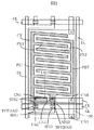
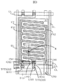
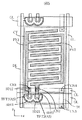
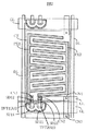
図8は本発明による液晶表示装置の一実施例を示す等価回路図である。図8に示す等価回路は、液晶を挟んで対向配置される各基板のうち一方の基板の液晶側の面に形成されたそれを示している。
Claims (7)
- 液晶を挟んで対向配置される一対の基板の内の一方の基板に、複数の画素領域を形成し、当該画素領域内に画素電極と対向電極とを備え、前記対向電極と前記画素電極は絶縁膜を介してお互いに重畳するように形成されている液晶表示装置であって、
前記各画素領域の画素電極は、第1の画素電極と第2の画素電極からなり、
前記画素領域には、更に、当該画素領域に映像信号を供給するドレイン信号線に接続された第1のスイッチング素子と第2のスイッチング素子を備え、
前記第1の画素電極は前記第1のスイッチング素子に接続され、前記第2の画素電極は前記第2のスイッチング素子に接続され、
前記第1及び第2の画素電極は交互に配置され、
前記各画素領域の対向電極は、ゲート信号線を間にして隣接する他の画素領域に配置される他の対向電極と、前記ゲート信号線をも被って形成される絶縁膜上に形成された導電層を介して互いに電気的に接続されていることを特徴とする液晶表示装置。 - 前記第1及び第2のスイッチング素子は共通のゲート信号線からの信号によってオンするように構成されていることを特徴とする請求項1に記載の液晶表示装置。
- 前記第1及び第2の画素電極のうち一方の画素電極は、前記画素領域を挟んで配置される一方のドレイン信号線に各電極を共通に接続する導電体が隣接して配置される櫛歯状のパターンをなすとともに、他方の画素電極は他方のドレイン信号線に各電極を共通に接続する導電体が隣接して配置される櫛歯状のパターンをなすことを特徴とする請求項1に記載の液晶表示装置。
- 前記各画素領域の対向電極は、ゲート信号線を間にして隣接する他の画素領域に配置される他の対向電極と、前記ゲート信号線をも被って形成される絶縁膜上に形成された導電層を介して互いに電気的に接続されていることを特徴とする請求項1に記載の液晶表示装置。
- 液晶を挟んで対向配置される一対の基板の内の一方の基板に、複数のゲート信号線とドレイン信号線の交差によって定義される複数の画素領域を形成し、当該各画素領域に画素電極と対向電極を備え、前記対向電極と前記画素電極は絶縁膜を介して形成されている液晶表示装置であって、
前記各画素領域の対向電極は、前記ドレイン信号線とゲート信号線に接しないように矩形状に形成され、
前記各画素領域の画素電極は、第1の画素電極と第2の画素電極からなり、前記第1の画素電極と前記第2の画素電極は、前記対向電極に重畳する位置に形成され、
前記画素領域には、更に、当該画素領域に映像信号を供給するドレイン信号線に接続された第1のスイッチング素子と第2のスイッチング素子を備え、
前記第1及び第2の画素電極は交互に配置され、
かつ、前記第1及び第2の薄膜トランジスタは共通の半導体層を有し、前記半導体層の上面に、前記半導体層と前記第1の画素電極を接続する第1のソース電極と、前記半導体層と前記第2の画素電極を接続する第2のソース電極と、前記第1のソース電極と対を成す第1のドレイン電極と、前記第1のソース電極と対を成す第2のドレイン電極を備えたことを特徴とする液晶表示装置。 - 前記第1及び第2のドレイン電極は、前記第1及び第2のソース電極の先端部を中心とした半円弧状をなすとともに、前記第1及び第2のドレイン電極は、互いに隣接する箇所において物理的に共通接続されていることを特徴とする請求項5に記載の液晶表示装置。
- 前記第1及び第2のドレイン電極の共通接続された部分における幅は、該部分以外の箇所の幅と同じになっていることを特徴とする請求項6に記載の液晶表示装置。
Priority Applications (6)
| Application Number | Priority Date | Filing Date | Title |
|---|---|---|---|
| JP2004274993A JP4606103B2 (ja) | 2004-09-22 | 2004-09-22 | 液晶表示装置 |
| US11/213,923 US7486363B2 (en) | 2004-09-22 | 2005-08-30 | Liquid crystal display device having first and second pixel electrodes overlapped to a counter electrode and connected to separate switching elements |
| CN2008101096468A CN101303498B (zh) | 2004-09-22 | 2005-09-21 | 液晶显示装置 |
| CNB2005101035475A CN100495175C (zh) | 2004-09-22 | 2005-09-21 | 液晶显示装置 |
| US12/232,156 US7643102B2 (en) | 2004-09-22 | 2008-09-11 | Liquid crystal display device having first and second pixel electrodes overlapping a common electrode and connected to first and second switching elements respectively |
| US12/591,403 US8144282B2 (en) | 2004-09-22 | 2009-11-18 | Liquid crystal display device having first and second pixel electrodes overlapping a common electrode and connected to first and second switching elements respectively |
Applications Claiming Priority (1)
| Application Number | Priority Date | Filing Date | Title |
|---|---|---|---|
| JP2004274993A JP4606103B2 (ja) | 2004-09-22 | 2004-09-22 | 液晶表示装置 |
Publications (3)
| Publication Number | Publication Date |
|---|---|
| JP2006091274A JP2006091274A (ja) | 2006-04-06 |
| JP2006091274A5 JP2006091274A5 (ja) | 2007-08-30 |
| JP4606103B2 true JP4606103B2 (ja) | 2011-01-05 |
Family
ID=36073554
Family Applications (1)
| Application Number | Title | Priority Date | Filing Date |
|---|---|---|---|
| JP2004274993A Active JP4606103B2 (ja) | 2004-09-22 | 2004-09-22 | 液晶表示装置 |
Country Status (3)
| Country | Link |
|---|---|
| US (3) | US7486363B2 (ja) |
| JP (1) | JP4606103B2 (ja) |
| CN (2) | CN100495175C (ja) |
Families Citing this family (21)
| Publication number | Priority date | Publication date | Assignee | Title |
|---|---|---|---|---|
| KR101240644B1 (ko) * | 2005-08-09 | 2013-03-11 | 삼성디스플레이 주식회사 | 박막 트랜지스터 표시판 |
| JP4884820B2 (ja) * | 2006-04-12 | 2012-02-29 | 株式会社 日立ディスプレイズ | 液晶表示装置 |
| TWI352868B (en) * | 2006-11-03 | 2011-11-21 | Au Optronics Corp | Liquid crystal display pannel and active device ar |
| KR101382481B1 (ko) * | 2007-09-03 | 2014-04-09 | 삼성디스플레이 주식회사 | 표시 장치 |
| EP2077466A1 (en) * | 2008-01-07 | 2009-07-08 | TPO Displays Corp. | Electrode structure for an LCD device |
| TWI333586B (en) * | 2008-02-19 | 2010-11-21 | Au Optronics Corp | Multi domain vertical alignment substrate and display device thereof |
| JP4730410B2 (ja) | 2008-03-27 | 2011-07-20 | エプソンイメージングデバイス株式会社 | 電気光学装置及び電子機器 |
| US8441731B2 (en) * | 2008-09-04 | 2013-05-14 | Innovega, Inc. | System and apparatus for pixel matrix see-through display panels |
| JP2010060857A (ja) * | 2008-09-04 | 2010-03-18 | Hitachi Displays Ltd | 液晶表示装置 |
| KR20100067481A (ko) * | 2008-12-11 | 2010-06-21 | 삼성전자주식회사 | 액정 표시 장치 |
| KR101542401B1 (ko) * | 2009-03-05 | 2015-08-07 | 삼성디스플레이 주식회사 | 액정 표시 장치 및 액정 표시 장치의 구동 방법 |
| US7932519B1 (en) * | 2009-12-28 | 2011-04-26 | Century Display(Shenzhen)Co.,Ltd. | Pixel structure |
| KR101733150B1 (ko) | 2010-03-05 | 2017-05-25 | 삼성디스플레이 주식회사 | 액정 표시 장치 |
| CN202443224U (zh) * | 2011-11-25 | 2012-09-19 | 北京京东方光电科技有限公司 | 像素结构及液晶面板 |
| TW201423206A (zh) * | 2012-12-14 | 2014-06-16 | Au Optronics Corp | 液晶顯示面板 |
| JP2014206639A (ja) * | 2013-04-12 | 2014-10-30 | 株式会社ジャパンディスプレイ | 液晶表示装置 |
| CN105785654A (zh) * | 2014-12-22 | 2016-07-20 | 业鑫科技顾问股份有限公司 | 液晶显示面板及其制作方法 |
| CN107482021B (zh) * | 2017-08-21 | 2020-01-24 | 京东方科技集团股份有限公司 | 阵列基板及显示装置 |
| CN207408720U (zh) * | 2017-11-01 | 2018-05-25 | 京东方科技集团股份有限公司 | 一种阵列基板和显示装置 |
| CN109557737B (zh) * | 2018-12-18 | 2020-10-16 | 武汉华星光电技术有限公司 | 一种阵列基板及显示面板 |
| CN109669305B (zh) * | 2019-02-21 | 2022-11-04 | 昆山龙腾光电股份有限公司 | 阵列基板和液晶显示面板 |
Citations (4)
| Publication number | Priority date | Publication date | Assignee | Title |
|---|---|---|---|---|
| JPH03196019A (ja) * | 1989-12-25 | 1991-08-27 | Mitsubishi Electric Corp | マトリクス型表示装置 |
| JPH08328043A (ja) * | 1995-02-01 | 1996-12-13 | Seiko Epson Corp | 液晶表示装置 |
| JP2001109018A (ja) * | 1999-10-12 | 2001-04-20 | Matsushita Electric Ind Co Ltd | 液晶表示装置およびその駆動方法 |
| WO2004023201A1 (en) * | 2002-09-09 | 2004-03-18 | Samsung Electronics Co., Ltd. | Multi-domain liquid crystal display and a thin film transistor substrate of the same |
Family Cites Families (22)
| Publication number | Priority date | Publication date | Assignee | Title |
|---|---|---|---|---|
| US5229644A (en) * | 1987-09-09 | 1993-07-20 | Casio Computer Co., Ltd. | Thin film transistor having a transparent electrode and substrate |
| JPH07119919B2 (ja) * | 1991-05-15 | 1995-12-20 | インターナショナル・ビジネス・マシーンズ・コーポレイション | 液晶表示装置 |
| US5532180A (en) * | 1995-06-02 | 1996-07-02 | Ois Optical Imaging Systems, Inc. | Method of fabricating a TFT with reduced channel length |
| JP3464570B2 (ja) * | 1995-08-21 | 2003-11-10 | 株式会社 日立ディスプレイズ | カラー液晶表示素子 |
| US6532053B2 (en) * | 1996-12-18 | 2003-03-11 | Hitachi, Ltd. | Transverse electric field system liquid crystal display device suitable for improving aperture ratio |
| US20010011981A1 (en) * | 1996-12-27 | 2001-08-09 | Tsunenori Yamamoto | Active matrix addressed liquid crystal display device |
| US5808706A (en) * | 1997-03-19 | 1998-09-15 | Samsung Electronics Co., Ltd. | Thin-film transistor liquid crystal display devices having cross-coupled storage capacitors |
| US6441401B1 (en) * | 1999-03-19 | 2002-08-27 | Samsung Electronics Co., Ltd. | Thin film transistor array panel for liquid crystal display and method for repairing the same |
| KR100311211B1 (ko) * | 1999-06-29 | 2001-11-02 | 박종섭 | 반사형 액정 표시 장치 |
| US6636289B2 (en) * | 2000-04-19 | 2003-10-21 | Lg.Philips Lcd Co., Ltd. | In-plane switching LCD panel with multiple domains and rubbing directions symetric about a line |
| KR100520381B1 (ko) * | 2000-05-31 | 2005-10-11 | 비오이 하이디스 테크놀로지 주식회사 | 프린지 필드 구동 액정표시장치 |
| JP3427981B2 (ja) * | 2000-07-05 | 2003-07-22 | 日本電気株式会社 | 液晶表示装置及びその製造方法 |
| KR100372577B1 (ko) * | 2000-08-07 | 2003-02-17 | 엘지.필립스 엘시디 주식회사 | 광시야각 액정 표시 장치 |
| JP4757393B2 (ja) * | 2001-03-23 | 2011-08-24 | Nec液晶テクノロジー株式会社 | 液晶表示装置及びその製造方法 |
| JP4647843B2 (ja) * | 2001-06-28 | 2011-03-09 | 株式会社日立製作所 | 液晶表示装置 |
| WO2003044595A1 (en) * | 2001-11-22 | 2003-05-30 | Samsung Electronics Co., Ltd. | Liquid crystal display and thin film transistor array panel |
| KR100905470B1 (ko) * | 2002-11-20 | 2009-07-02 | 삼성전자주식회사 | 박막 트랜지스터 어레이 기판 |
| KR100951348B1 (ko) * | 2003-04-04 | 2010-04-08 | 삼성전자주식회사 | 다중 도메인 액정 표시 장치 및 그 박막 트랜지스터 기판 |
| KR20040105934A (ko) * | 2003-06-10 | 2004-12-17 | 삼성전자주식회사 | 다중 도메인 액정 표시 장치 및 그에 사용되는 표시판 |
| KR100698049B1 (ko) * | 2003-06-26 | 2007-03-23 | 엘지.필립스 엘시디 주식회사 | 액정표시장치 및 그의 제조방법 |
| US7206048B2 (en) * | 2003-08-13 | 2007-04-17 | Samsung Electronics Co., Ltd. | Liquid crystal display and panel therefor |
| JP4381782B2 (ja) * | 2003-11-18 | 2009-12-09 | 株式会社 日立ディスプレイズ | 液晶表示装置 |
-
2004
- 2004-09-22 JP JP2004274993A patent/JP4606103B2/ja active Active
-
2005
- 2005-08-30 US US11/213,923 patent/US7486363B2/en active Active
- 2005-09-21 CN CNB2005101035475A patent/CN100495175C/zh active Active
- 2005-09-21 CN CN2008101096468A patent/CN101303498B/zh active Active
-
2008
- 2008-09-11 US US12/232,156 patent/US7643102B2/en active Active
-
2009
- 2009-11-18 US US12/591,403 patent/US8144282B2/en active Active
Patent Citations (4)
| Publication number | Priority date | Publication date | Assignee | Title |
|---|---|---|---|---|
| JPH03196019A (ja) * | 1989-12-25 | 1991-08-27 | Mitsubishi Electric Corp | マトリクス型表示装置 |
| JPH08328043A (ja) * | 1995-02-01 | 1996-12-13 | Seiko Epson Corp | 液晶表示装置 |
| JP2001109018A (ja) * | 1999-10-12 | 2001-04-20 | Matsushita Electric Ind Co Ltd | 液晶表示装置およびその駆動方法 |
| WO2004023201A1 (en) * | 2002-09-09 | 2004-03-18 | Samsung Electronics Co., Ltd. | Multi-domain liquid crystal display and a thin film transistor substrate of the same |
Also Published As
| Publication number | Publication date |
|---|---|
| CN100495175C (zh) | 2009-06-03 |
| CN101303498B (zh) | 2011-09-07 |
| US7643102B2 (en) | 2010-01-05 |
| JP2006091274A (ja) | 2006-04-06 |
| US20060061723A1 (en) | 2006-03-23 |
| US20100066935A1 (en) | 2010-03-18 |
| US7486363B2 (en) | 2009-02-03 |
| US20090015775A1 (en) | 2009-01-15 |
| CN101303498A (zh) | 2008-11-12 |
| CN1752827A (zh) | 2006-03-29 |
| US8144282B2 (en) | 2012-03-27 |
Similar Documents
| Publication | Publication Date | Title |
|---|---|---|
| JP4606103B2 (ja) | 液晶表示装置 | |
| JP5448875B2 (ja) | 液晶表示装置 | |
| JP4381782B2 (ja) | 液晶表示装置 | |
| JP5165169B2 (ja) | 液晶表示装置 | |
| JP5876526B2 (ja) | 液晶表示装置 | |
| JP4326307B2 (ja) | 液晶表示装置 | |
| JP4516348B2 (ja) | 液晶表示装置 | |
| JP3712899B2 (ja) | 液晶表示装置 | |
| KR100966452B1 (ko) | 수평전계방식 액정표시소자 및 그 제조방법 | |
| JP4364925B2 (ja) | アクティブマトリクス基板、液晶パネル、液晶表示装置、テレビジョン受像機 | |
| JP2009223245A (ja) | 液晶表示装置 | |
| JP2003195330A (ja) | 液晶表示装置 | |
| JP4424925B2 (ja) | 表示装置 | |
| JP5551553B2 (ja) | 液晶表示装置 | |
| JP4217170B2 (ja) | 液晶表示装置およびその駆動方法 | |
| JP2004177788A (ja) | 液晶表示装置 | |
| JP4584614B2 (ja) | 液晶表示装置 | |
| JP4381785B2 (ja) | 液晶表示装置 | |
| JP2009080376A (ja) | 液晶表示装置 | |
| JP5595678B2 (ja) | 液晶表示装置 | |
| JP2003057670A (ja) | 液晶表示装置 | |
| KR100852807B1 (ko) | 프린지 필드 스위칭 모드 액정표시장치 | |
| KR20080024963A (ko) | 액정 표시 장치 | |
| JP2007139934A (ja) | 液晶表示装置 | |
| JP5513052B2 (ja) | 液晶表示装置 |
Legal Events
| Date | Code | Title | Description |
|---|---|---|---|
| A521 | Request for written amendment filed |
Free format text: JAPANESE INTERMEDIATE CODE: A523 Effective date: 20070711 |
|
| A621 | Written request for application examination |
Free format text: JAPANESE INTERMEDIATE CODE: A621 Effective date: 20070711 |
|
| A977 | Report on retrieval |
Free format text: JAPANESE INTERMEDIATE CODE: A971007 Effective date: 20100616 |
|
| A131 | Notification of reasons for refusal |
Free format text: JAPANESE INTERMEDIATE CODE: A131 Effective date: 20100706 |
|
| A521 | Request for written amendment filed |
Free format text: JAPANESE INTERMEDIATE CODE: A523 Effective date: 20100903 |
|
| TRDD | Decision of grant or rejection written | ||
| A01 | Written decision to grant a patent or to grant a registration (utility model) |
Free format text: JAPANESE INTERMEDIATE CODE: A01 Effective date: 20100928 |
|
| A01 | Written decision to grant a patent or to grant a registration (utility model) |
Free format text: JAPANESE INTERMEDIATE CODE: A01 |
|
| A61 | First payment of annual fees (during grant procedure) |
Free format text: JAPANESE INTERMEDIATE CODE: A61 Effective date: 20101005 |
|
| R150 | Certificate of patent or registration of utility model |
Ref document number: 4606103 Country of ref document: JP Free format text: JAPANESE INTERMEDIATE CODE: R150 Free format text: JAPANESE INTERMEDIATE CODE: R150 |
|
| FPAY | Renewal fee payment (event date is renewal date of database) |
Free format text: PAYMENT UNTIL: 20131015 Year of fee payment: 3 |
|
| FPAY | Renewal fee payment (event date is renewal date of database) |
Free format text: PAYMENT UNTIL: 20131015 Year of fee payment: 3 |
|
| S111 | Request for change of ownership or part of ownership |
Free format text: JAPANESE INTERMEDIATE CODE: R313121 Free format text: JAPANESE INTERMEDIATE CODE: R313115 |
|
| FPAY | Renewal fee payment (event date is renewal date of database) |
Free format text: PAYMENT UNTIL: 20131015 Year of fee payment: 3 |
|
| R350 | Written notification of registration of transfer |
Free format text: JAPANESE INTERMEDIATE CODE: R350 |
|
| R250 | Receipt of annual fees |
Free format text: JAPANESE INTERMEDIATE CODE: R250 |
|
| R250 | Receipt of annual fees |
Free format text: JAPANESE INTERMEDIATE CODE: R250 |
|
| R250 | Receipt of annual fees |
Free format text: JAPANESE INTERMEDIATE CODE: R250 |
|
| R250 | Receipt of annual fees |
Free format text: JAPANESE INTERMEDIATE CODE: R250 |
|
| R250 | Receipt of annual fees |
Free format text: JAPANESE INTERMEDIATE CODE: R250 |
|
| R250 | Receipt of annual fees |
Free format text: JAPANESE INTERMEDIATE CODE: R250 |
|
| R250 | Receipt of annual fees |
Free format text: JAPANESE INTERMEDIATE CODE: R250 |
|
| R250 | Receipt of annual fees |
Free format text: JAPANESE INTERMEDIATE CODE: R250 |
|
| S531 | Written request for registration of change of domicile |
Free format text: JAPANESE INTERMEDIATE CODE: R313531 |
|
| S533 | Written request for registration of change of name |
Free format text: JAPANESE INTERMEDIATE CODE: R313533 |
|
| R350 | Written notification of registration of transfer |
Free format text: JAPANESE INTERMEDIATE CODE: R350 |
|
| R250 | Receipt of annual fees |
Free format text: JAPANESE INTERMEDIATE CODE: R250 |
|
| R250 | Receipt of annual fees |
Free format text: JAPANESE INTERMEDIATE CODE: R250 |
|
| S111 | Request for change of ownership or part of ownership |
Free format text: JAPANESE INTERMEDIATE CODE: R313117 |
|
| R350 | Written notification of registration of transfer |
Free format text: JAPANESE INTERMEDIATE CODE: R350 |
|
| R250 | Receipt of annual fees |
Free format text: JAPANESE INTERMEDIATE CODE: R250 |