JP4515143B2 - 感熱式流量検出素子の製造方法 - Google Patents
感熱式流量検出素子の製造方法 Download PDFInfo
- Publication number
- JP4515143B2 JP4515143B2 JP2004139533A JP2004139533A JP4515143B2 JP 4515143 B2 JP4515143 B2 JP 4515143B2 JP 2004139533 A JP2004139533 A JP 2004139533A JP 2004139533 A JP2004139533 A JP 2004139533A JP 4515143 B2 JP4515143 B2 JP 4515143B2
- Authority
- JP
- Japan
- Prior art keywords
- flow rate
- rate detection
- dummy pattern
- manufacturing
- film
- Prior art date
- Legal status (The legal status is an assumption and is not a legal conclusion. Google has not performed a legal analysis and makes no representation as to the accuracy of the status listed.)
- Expired - Fee Related
Links
- 238000001514 detection method Methods 0.000 title claims description 66
- 238000004519 manufacturing process Methods 0.000 title claims description 49
- 238000000034 method Methods 0.000 title claims description 32
- 239000000758 substrate Substances 0.000 claims description 49
- 238000010438 heat treatment Methods 0.000 claims description 32
- 230000001681 protective effect Effects 0.000 claims description 28
- 238000007689 inspection Methods 0.000 claims description 17
- XLYOFNOQVPJJNP-UHFFFAOYSA-N water Substances O XLYOFNOQVPJJNP-UHFFFAOYSA-N 0.000 claims description 15
- 238000000926 separation method Methods 0.000 claims description 2
- 239000010408 film Substances 0.000 description 72
- 230000007547 defect Effects 0.000 description 17
- 239000010409 thin film Substances 0.000 description 17
- BASFCYQUMIYNBI-UHFFFAOYSA-N platinum Chemical compound [Pt] BASFCYQUMIYNBI-UHFFFAOYSA-N 0.000 description 13
- WGTYBPLFGIVFAS-UHFFFAOYSA-M tetramethylammonium hydroxide Chemical compound [OH-].C[N+](C)(C)C WGTYBPLFGIVFAS-UHFFFAOYSA-M 0.000 description 8
- 229910052697 platinum Inorganic materials 0.000 description 7
- 238000004544 sputter deposition Methods 0.000 description 7
- 229910052581 Si3N4 Inorganic materials 0.000 description 6
- 238000005530 etching Methods 0.000 description 6
- 238000000206 photolithography Methods 0.000 description 6
- HQVNEWCFYHHQES-UHFFFAOYSA-N silicon nitride Chemical compound N12[Si]34N5[Si]62N3[Si]51N64 HQVNEWCFYHHQES-UHFFFAOYSA-N 0.000 description 6
- 238000000151 deposition Methods 0.000 description 5
- 238000005868 electrolysis reaction Methods 0.000 description 5
- 239000000463 material Substances 0.000 description 5
- 238000012545 processing Methods 0.000 description 5
- 238000001312 dry etching Methods 0.000 description 4
- 238000001039 wet etching Methods 0.000 description 4
- 230000007423 decrease Effects 0.000 description 3
- 239000012530 fluid Substances 0.000 description 3
- 229910052710 silicon Inorganic materials 0.000 description 3
- 239000010703 silicon Substances 0.000 description 3
- 238000007740 vapor deposition Methods 0.000 description 3
- HEMHJVSKTPXQMS-UHFFFAOYSA-M Sodium hydroxide Chemical compound [OH-].[Na+] HEMHJVSKTPXQMS-UHFFFAOYSA-M 0.000 description 2
- 239000003513 alkali Substances 0.000 description 2
- 239000013078 crystal Substances 0.000 description 2
- 238000010586 diagram Methods 0.000 description 2
- 230000000694 effects Effects 0.000 description 2
- 230000000087 stabilizing effect Effects 0.000 description 2
- 238000012360 testing method Methods 0.000 description 2
- 238000009529 body temperature measurement Methods 0.000 description 1
- 238000002485 combustion reaction Methods 0.000 description 1
- 239000004020 conductor Substances 0.000 description 1
- 238000007796 conventional method Methods 0.000 description 1
- 230000007797 corrosion Effects 0.000 description 1
- 238000005260 corrosion Methods 0.000 description 1
- 230000001419 dependent effect Effects 0.000 description 1
- 230000006866 deterioration Effects 0.000 description 1
- 238000001035 drying Methods 0.000 description 1
- 230000020169 heat generation Effects 0.000 description 1
- 239000010410 layer Substances 0.000 description 1
- 238000000059 patterning Methods 0.000 description 1
- 150000003057 platinum Chemical class 0.000 description 1
- 239000011241 protective layer Substances 0.000 description 1
- 230000035945 sensitivity Effects 0.000 description 1
- 239000000126 substance Substances 0.000 description 1
- 230000000007 visual effect Effects 0.000 description 1
Images


Classifications
-
- G—PHYSICS
- G01—MEASURING; TESTING
- G01F—MEASURING VOLUME, VOLUME FLOW, MASS FLOW OR LIQUID LEVEL; METERING BY VOLUME
- G01F1/00—Measuring the volume flow or mass flow of fluid or fluent solid material wherein the fluid passes through a meter in a continuous flow
- G01F1/68—Measuring the volume flow or mass flow of fluid or fluent solid material wherein the fluid passes through a meter in a continuous flow by using thermal effects
-
- H—ELECTRICITY
- H01—ELECTRIC ELEMENTS
- H01L—SEMICONDUCTOR DEVICES NOT COVERED BY CLASS H10
- H01L27/00—Devices consisting of a plurality of semiconductor or other solid-state components formed in or on a common substrate
- H01L27/14—Devices consisting of a plurality of semiconductor or other solid-state components formed in or on a common substrate including semiconductor components sensitive to infrared radiation, light, electromagnetic radiation of shorter wavelength or corpuscular radiation and specially adapted either for the conversion of the energy of such radiation into electrical energy or for the control of electrical energy by such radiation
- H01L27/144—Devices controlled by radiation
- H01L27/146—Imager structures
- H01L27/14683—Processes or apparatus peculiar to the manufacture or treatment of these devices or parts thereof
- H01L27/14687—Wafer level processing
-
- H—ELECTRICITY
- H01—ELECTRIC ELEMENTS
- H01L—SEMICONDUCTOR DEVICES NOT COVERED BY CLASS H10
- H01L27/00—Devices consisting of a plurality of semiconductor or other solid-state components formed in or on a common substrate
- H01L27/14—Devices consisting of a plurality of semiconductor or other solid-state components formed in or on a common substrate including semiconductor components sensitive to infrared radiation, light, electromagnetic radiation of shorter wavelength or corpuscular radiation and specially adapted either for the conversion of the energy of such radiation into electrical energy or for the control of electrical energy by such radiation
- H01L27/144—Devices controlled by radiation
- H01L27/146—Imager structures
- H01L27/14643—Photodiode arrays; MOS imagers
Description
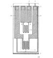
図1は、実施の形態1に係る感熱式の流量検出素子12の製造工程における基板上の配置を示す上面図である。また、図2は、図1に示される流量検出素子12の構造を示す上面図である。また、図3は、図2に示される流量検出素子12の構造を示す断面図である。図1,2においては、図示の都合上、図3に示される保護膜3は省略している。
実施の形態1に係る感熱式流量検出素子の製造方法においては、基板1を水17に浸漬させた状態で通電し、水17の電気分解をチェックすることにより、カバレッジ欠陥の検査を行っている。しかし、水17に浸漬させる代わりに、保護膜3上に導電性膜を形成し、この導電性膜を用いてカバレッジ欠陥の検査を行ってもよい。
Claims (7)
- 基板上に形成された絶縁性の支持膜と前記基板を部分的に除去することにより形成されたダイヤフラムとを有する感熱式流量検出素子の製造方法であって、
感熱抵抗膜からなり発熱用抵抗体および測温用抵抗体を有する流量検出用パターンを前記支持膜上に複数個形成する流量検出用パターン形成工程と、
前記感熱抵抗膜からなり複数の前記流量検出用パターンを電気的に接続させるためのダミーパターンを前記支持膜上に形成するダミーパターン形成工程と、
前記流量検出用パターンおよび前記ダミーパターン上に保護膜を形成する工程と、
前記ダミーパターンを用いて複数の前記流量検出用パターンに対し所定の処理を実行する工程と、
複数の前記流量検出用パターンを個々に分離し前記ダミーパターンによる接続から解放する工程と
を備え、
前記所定の処理は、前記保護膜で覆われ前記ダミーパターンにより接続された複数の前記流量検出用パターンを水に浸漬させた状態で通電することによる前記保護膜の検査を含む
ことを特徴とする感熱式流量検出素子の製造方法。 - 請求項1に記載の感熱式流量検出素子の製造方法であって、
前記ダミーパターンを電気的に外部と接続させるためのダミーパターン用電極を形成する工程
をさらに備えることを特徴とする感熱式流量検出素子の製造方法。 - 請求項1又は請求項2に記載の感熱式流量検出素子の製造方法であって、
前記ダミーパターン形成工程において、前記ダミーパターンは、隣接する前記流量検出用パターン同士において前記発熱用抵抗体同士を並列に電気的に接続させるように形成される
ことを特徴とする感熱式流量検出素子の製造方法。 - 請求項1乃至請求項3のいずれかに記載の感熱式流量検出素子の製造方法であって、
前記ダミーパターンの分離端を保護膜で覆う工程
をさらに備えることを特徴とする感熱式流量検出素子の製造方法。 - 請求項1乃至請求項4のいずれかに記載の感熱式流量検出素子の製造方法であって、
前記ダミーパターン形成工程において、前記ダミーパターンは、隣接する前記流量検出用パターン同士において前記測温用抵抗体を電気的に接続させるように形成される
ことを特徴とする感熱式流量検出素子の製造方法。 - 請求項1乃至請求項5のいずれかに記載の感熱式流量検出素子の製造方法であって、
前記流量検出用パターンおよび前記ダミーパターン上に保護膜を形成し、さらにその上に導電性膜を形成する工程
をさらに備えることを特徴とする感熱式流量検出素子の製造方法。 - 請求項1乃至請求項6のいずれかに記載の感熱式流量検出素子の製造方法であって、
前記流量検出用パターン形成工程と前記ダミーパターン形成工程とは同一の工程において行われる
ことを特徴とする感熱式流量検出素子の製造方法。
Priority Applications (4)
| Application Number | Priority Date | Filing Date | Title |
|---|---|---|---|
| JP2004139533A JP4515143B2 (ja) | 2004-05-10 | 2004-05-10 | 感熱式流量検出素子の製造方法 |
| US10/944,390 US6995028B2 (en) | 2004-05-10 | 2004-09-20 | Method of manufacturing thermal type flow sensing elements |
| KR1020040083109A KR100592177B1 (ko) | 2004-05-10 | 2004-10-18 | 감열식 유량 검출 소자의 제조 방법 |
| DE102004052634A DE102004052634B4 (de) | 2004-05-10 | 2004-10-29 | Verfahren zur Herstellung von Wärme-Flussmesselementen |
Applications Claiming Priority (1)
| Application Number | Priority Date | Filing Date | Title |
|---|---|---|---|
| JP2004139533A JP4515143B2 (ja) | 2004-05-10 | 2004-05-10 | 感熱式流量検出素子の製造方法 |
Publications (3)
| Publication Number | Publication Date |
|---|---|
| JP2005321294A JP2005321294A (ja) | 2005-11-17 |
| JP2005321294A5 JP2005321294A5 (ja) | 2007-04-12 |
| JP4515143B2 true JP4515143B2 (ja) | 2010-07-28 |
Family
ID=35239924
Family Applications (1)
| Application Number | Title | Priority Date | Filing Date |
|---|---|---|---|
| JP2004139533A Expired - Fee Related JP4515143B2 (ja) | 2004-05-10 | 2004-05-10 | 感熱式流量検出素子の製造方法 |
Country Status (4)
| Country | Link |
|---|---|
| US (1) | US6995028B2 (ja) |
| JP (1) | JP4515143B2 (ja) |
| KR (1) | KR100592177B1 (ja) |
| DE (1) | DE102004052634B4 (ja) |
Families Citing this family (3)
| Publication number | Priority date | Publication date | Assignee | Title |
|---|---|---|---|---|
| US20130313675A1 (en) * | 2011-03-02 | 2013-11-28 | Hitachi Automotive Systems ,Ltd. | Thermal Type Flowmeter |
| DE112011105438B4 (de) * | 2011-07-13 | 2020-06-18 | Hitachi Automotive Systems, Ltd. | Durchflussmengenmesser |
| JP6475198B2 (ja) * | 2016-06-29 | 2019-02-27 | 太陽誘電株式会社 | 可変容量デバイス及びアンテナ装置 |
Citations (4)
| Publication number | Priority date | Publication date | Assignee | Title |
|---|---|---|---|---|
| JPS6397237U (ja) * | 1986-12-12 | 1988-06-23 | ||
| JPH10206205A (ja) * | 1997-01-22 | 1998-08-07 | Ricoh Co Ltd | マイクロブリッジセンサの製造方法 |
| JP2001056310A (ja) * | 1999-08-20 | 2001-02-27 | Sony Corp | 半導体装置の検査方法 |
| WO2001084088A1 (fr) * | 2000-05-02 | 2001-11-08 | Hitachi, Ltd. | Dispositif de mesure d'une quantite physique, procede de fabrication associe, et systeme de commande de vehicule mettant en oeuvre ce dispositif de mesure de quantite physique |
Family Cites Families (13)
| Publication number | Priority date | Publication date | Assignee | Title |
|---|---|---|---|---|
| US3849872A (en) * | 1972-10-24 | 1974-11-26 | Ibm | Contacting integrated circuit chip terminal through the wafer kerf |
| US4426773A (en) * | 1981-05-15 | 1984-01-24 | General Electric Ceramics, Inc. | Array of electronic packaging substrates |
| US4855253A (en) * | 1988-01-29 | 1989-08-08 | Hewlett-Packard | Test method for random defects in electronic microstructures |
| US5389556A (en) * | 1992-07-02 | 1995-02-14 | Lsi Logic Corporation | Individually powering-up unsingulated dies on a wafer |
| US5532174A (en) * | 1994-04-22 | 1996-07-02 | Lsi Logic Corporation | Wafer level integrated circuit testing with a sacrificial metal layer |
| US6744346B1 (en) * | 1998-02-27 | 2004-06-01 | Micron Technology, Inc. | Electronic device workpieces, methods of semiconductor processing and methods of sensing temperature of an electronic device workpiece |
| JP3513041B2 (ja) * | 1999-01-25 | 2004-03-31 | 三菱電機株式会社 | 流量センサ |
| JP3455473B2 (ja) * | 1999-07-14 | 2003-10-14 | 三菱電機株式会社 | 感熱式流量センサ |
| JP3461469B2 (ja) * | 1999-07-27 | 2003-10-27 | 株式会社日立製作所 | 熱式空気流量センサ及び内燃機関制御装置 |
| US6133054A (en) * | 1999-08-02 | 2000-10-17 | Motorola, Inc. | Method and apparatus for testing an integrated circuit |
| US6225141B1 (en) * | 1999-09-03 | 2001-05-01 | Johnson Controls Technology Co. | Temperature sensor manufacturing process |
| JP5138134B2 (ja) * | 2001-07-16 | 2013-02-06 | 株式会社デンソー | 薄膜式センサの製造方法ならびにフローセンサの製造方法 |
| US6844218B2 (en) * | 2001-12-27 | 2005-01-18 | Texas Instruments Incorporated | Semiconductor wafer with grouped integrated circuit die having inter-die connections for group testing |
-
2004
- 2004-05-10 JP JP2004139533A patent/JP4515143B2/ja not_active Expired - Fee Related
- 2004-09-20 US US10/944,390 patent/US6995028B2/en active Active
- 2004-10-18 KR KR1020040083109A patent/KR100592177B1/ko active IP Right Grant
- 2004-10-29 DE DE102004052634A patent/DE102004052634B4/de not_active Expired - Fee Related
Patent Citations (4)
| Publication number | Priority date | Publication date | Assignee | Title |
|---|---|---|---|---|
| JPS6397237U (ja) * | 1986-12-12 | 1988-06-23 | ||
| JPH10206205A (ja) * | 1997-01-22 | 1998-08-07 | Ricoh Co Ltd | マイクロブリッジセンサの製造方法 |
| JP2001056310A (ja) * | 1999-08-20 | 2001-02-27 | Sony Corp | 半導体装置の検査方法 |
| WO2001084088A1 (fr) * | 2000-05-02 | 2001-11-08 | Hitachi, Ltd. | Dispositif de mesure d'une quantite physique, procede de fabrication associe, et systeme de commande de vehicule mettant en oeuvre ce dispositif de mesure de quantite physique |
Also Published As
| Publication number | Publication date |
|---|---|
| JP2005321294A (ja) | 2005-11-17 |
| KR100592177B1 (ko) | 2006-06-26 |
| US20050250239A1 (en) | 2005-11-10 |
| US6995028B2 (en) | 2006-02-07 |
| DE102004052634A1 (de) | 2005-12-08 |
| DE102004052634B4 (de) | 2012-04-19 |
| KR20050107727A (ko) | 2005-11-15 |
Similar Documents
| Publication | Publication Date | Title |
|---|---|---|
| US7180302B2 (en) | Method and system for determining cracks and broken components in armor | |
| JP4902679B2 (ja) | 計測素子 | |
| JP2017161325A (ja) | ガスセンサの検査方法およびガスセンサの製造方法 | |
| JP4515143B2 (ja) | 感熱式流量検出素子の製造方法 | |
| US6845662B2 (en) | Thermosensitive flow rate detecting element and method for the manufacture thereof | |
| JP2011174876A (ja) | ダイアフラム部を有する基板を備えたセンサ装置、及び同センサ装置を複数備えたセンサ装置アレイ | |
| JP3853260B2 (ja) | 評価用素子を含む半導体装置及び該評価用素子を用いた故障解析方法 | |
| JP4746609B2 (ja) | 半導体装置及びその製造方法 | |
| CN106158743B (zh) | 利用多感应像素检测多种气体的传感器的制造方法 | |
| JP3741086B2 (ja) | 絶縁分離型半導体装置のための評価用半導体基板及び絶縁不良評価方法 | |
| TWI445973B (zh) | 電氣連接裝置及使用其之測試裝置 | |
| KR101820675B1 (ko) | 다층 저항식 다점 온도측정 웨이퍼 센서 및 그 제조방법 | |
| JP4487424B2 (ja) | 薄膜部を有するセンサの検査方法 | |
| JP4912056B2 (ja) | プローバ用チャック | |
| CN1129529C (zh) | 喷墨印头芯片及喷墨印头寿命与缺陷的检测方法 | |
| JP2002198576A (ja) | 半導体装置 | |
| JP3524049B2 (ja) | 配線パタ−ンの検査方法 | |
| JP2006013225A (ja) | 異物検出用teg、異物検出装置及び異物検出方法 | |
| JP2008211118A (ja) | 帯電量評価素子 | |
| JP4428945B2 (ja) | 圧電アクチュエータの評価方法及び液滴吐出装置の製造方法 | |
| KR101746558B1 (ko) | 다층 저항식 다점 온도측정 웨이퍼 센서 및 그 제조방법 | |
| JP4179004B2 (ja) | 半導体センサ装置 | |
| CN117949813A (zh) | 芯片检测电路及方法 | |
| JP6180900B2 (ja) | 応力検知用素子および応力検知方法 | |
| JP2000250057A (ja) | 液晶表示装置における透明電極パターンの検査方法 |
Legal Events
| Date | Code | Title | Description |
|---|---|---|---|
| A521 | Written amendment |
Free format text: JAPANESE INTERMEDIATE CODE: A523 Effective date: 20070223 |
|
| A621 | Written request for application examination |
Free format text: JAPANESE INTERMEDIATE CODE: A621 Effective date: 20070223 |
|
| RD04 | Notification of resignation of power of attorney |
Free format text: JAPANESE INTERMEDIATE CODE: A7424 Effective date: 20091118 |
|
| A977 | Report on retrieval |
Free format text: JAPANESE INTERMEDIATE CODE: A971007 Effective date: 20091207 |
|
| A131 | Notification of reasons for refusal |
Free format text: JAPANESE INTERMEDIATE CODE: A131 Effective date: 20091215 |
|
| A521 | Written amendment |
Free format text: JAPANESE INTERMEDIATE CODE: A523 Effective date: 20100203 |
|
| A131 | Notification of reasons for refusal |
Free format text: JAPANESE INTERMEDIATE CODE: A131 Effective date: 20100223 |
|
| A521 | Written amendment |
Free format text: JAPANESE INTERMEDIATE CODE: A523 Effective date: 20100420 |
|
| TRDD | Decision of grant or rejection written | ||
| A01 | Written decision to grant a patent or to grant a registration (utility model) |
Free format text: JAPANESE INTERMEDIATE CODE: A01 Effective date: 20100511 |
|
| A01 | Written decision to grant a patent or to grant a registration (utility model) |
Free format text: JAPANESE INTERMEDIATE CODE: A01 |
|
| A61 | First payment of annual fees (during grant procedure) |
Free format text: JAPANESE INTERMEDIATE CODE: A61 Effective date: 20100512 |
|
| R150 | Certificate of patent or registration of utility model |
Ref document number: 4515143 Country of ref document: JP Free format text: JAPANESE INTERMEDIATE CODE: R150 Free format text: JAPANESE INTERMEDIATE CODE: R150 |
|
| FPAY | Renewal fee payment (event date is renewal date of database) |
Free format text: PAYMENT UNTIL: 20130521 Year of fee payment: 3 |
|
| FPAY | Renewal fee payment (event date is renewal date of database) |
Free format text: PAYMENT UNTIL: 20140521 Year of fee payment: 4 |
|
| R250 | Receipt of annual fees |
Free format text: JAPANESE INTERMEDIATE CODE: R250 |
|
| R250 | Receipt of annual fees |
Free format text: JAPANESE INTERMEDIATE CODE: R250 |
|
| R250 | Receipt of annual fees |
Free format text: JAPANESE INTERMEDIATE CODE: R250 |
|
| R250 | Receipt of annual fees |
Free format text: JAPANESE INTERMEDIATE CODE: R250 |
|
| R250 | Receipt of annual fees |
Free format text: JAPANESE INTERMEDIATE CODE: R250 |
|
| LAPS | Cancellation because of no payment of annual fees |