JP4444693B2 - 光学波長板の製造方法 - Google Patents
光学波長板の製造方法 Download PDFInfo
- Publication number
- JP4444693B2 JP4444693B2 JP2004053252A JP2004053252A JP4444693B2 JP 4444693 B2 JP4444693 B2 JP 4444693B2 JP 2004053252 A JP2004053252 A JP 2004053252A JP 2004053252 A JP2004053252 A JP 2004053252A JP 4444693 B2 JP4444693 B2 JP 4444693B2
- Authority
- JP
- Japan
- Prior art keywords
- heat treatment
- phase difference
- etching
- dielectric
- dielectric medium
- Prior art date
- Legal status (The legal status is an assumption and is not a legal conclusion. Google has not performed a legal analysis and makes no representation as to the accuracy of the status listed.)
- Expired - Fee Related
Links
Images


Classifications
-
- G—PHYSICS
- G02—OPTICS
- G02B—OPTICAL ELEMENTS, SYSTEMS OR APPARATUS
- G02B5/00—Optical elements other than lenses
- G02B5/18—Diffraction gratings
- G02B5/1847—Manufacturing methods
- G02B5/1857—Manufacturing methods using exposure or etching means, e.g. holography, photolithography, exposure to electron or ion beams
-
- G—PHYSICS
- G02—OPTICS
- G02B—OPTICAL ELEMENTS, SYSTEMS OR APPARATUS
- G02B5/00—Optical elements other than lenses
- G02B5/30—Polarising elements
- G02B5/3083—Birefringent or phase retarding elements
-
- Y—GENERAL TAGGING OF NEW TECHNOLOGICAL DEVELOPMENTS; GENERAL TAGGING OF CROSS-SECTIONAL TECHNOLOGIES SPANNING OVER SEVERAL SECTIONS OF THE IPC; TECHNICAL SUBJECTS COVERED BY FORMER USPC CROSS-REFERENCE ART COLLECTIONS [XRACs] AND DIGESTS
- Y10—TECHNICAL SUBJECTS COVERED BY FORMER USPC
- Y10T—TECHNICAL SUBJECTS COVERED BY FORMER US CLASSIFICATION
- Y10T428/00—Stock material or miscellaneous articles
- Y10T428/24—Structurally defined web or sheet [e.g., overall dimension, etc.]
- Y10T428/24479—Structurally defined web or sheet [e.g., overall dimension, etc.] including variation in thickness
- Y10T428/24612—Composite web or sheet
-
- Y—GENERAL TAGGING OF NEW TECHNOLOGICAL DEVELOPMENTS; GENERAL TAGGING OF CROSS-SECTIONAL TECHNOLOGIES SPANNING OVER SEVERAL SECTIONS OF THE IPC; TECHNICAL SUBJECTS COVERED BY FORMER USPC CROSS-REFERENCE ART COLLECTIONS [XRACs] AND DIGESTS
- Y10—TECHNICAL SUBJECTS COVERED BY FORMER USPC
- Y10T—TECHNICAL SUBJECTS COVERED BY FORMER US CLASSIFICATION
- Y10T428/00—Stock material or miscellaneous articles
- Y10T428/24—Structurally defined web or sheet [e.g., overall dimension, etc.]
- Y10T428/24802—Discontinuous or differential coating, impregnation or bond [e.g., artwork, printing, retouched photograph, etc.]
Description
na={n1 2+n2 2(1−q)}1/2・・・・(1)
nb={(1/n1)2q+(1/n2)2(1−q)}-1/2・・・・(2)
Δn=|na―nb|・・・・(3)
ΔΦ[rad]=(2πD/λ)Δn・・・・(4)
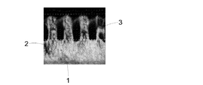
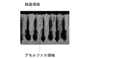
2 誘電体媒質
3 矩形格子
11 熱処理装置
12 熱源
Claims (2)
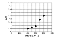
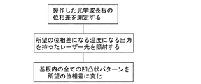
- 少なくとも1つの誘電体媒質を基板上にアモルファス状態で成膜し、前記誘電体媒質をエッチングして可視光の波長よりも短い周期構造を有する凹凸状格子パターンを製造し、前記エッチングした前記誘電体媒質を熱処理により結晶化させて膜の屈折率を大きくし、前記熱処理における熱処理温度を変えることにより、前記凹凸状格子パターンの位相差の大きさを制御することを特徴とする光学波長板の製造方法。
- 少なくとも1つの誘電体媒質を基板上にアモルファス状態で成膜し、前記誘電体媒質をエッチングして可視光の波長よりも短い周期構造を有する凹凸状格子パターンを製造し、前記エッチングした前記誘電体媒質を熱処理により結晶化させて膜の屈折率を大きくし、前記誘電体媒質をエッチングして製造した前記凹凸状格子パターンの位相差の均一性が悪いとき、前記位相差に適した温度で熱処理し前記位相差を揃えることを特徴とする光学波長板の製造方法。
Priority Applications (4)
| Application Number | Priority Date | Filing Date | Title |
|---|---|---|---|
| JP2004053252A JP4444693B2 (ja) | 2004-02-27 | 2004-02-27 | 光学波長板の製造方法 |
| US11/064,602 US7428101B2 (en) | 2004-02-27 | 2005-02-24 | Optical retardation plate and method of manufacturing the same |
| EP05251146A EP1569014B1 (en) | 2004-02-27 | 2005-02-25 | Optical retardation plate and method of manufacturing the same |
| DE602005007782T DE602005007782D1 (de) | 2004-02-27 | 2005-02-25 | Optische Verzögerungsplatte und Verfahren zu ihrer Herstellung |
Applications Claiming Priority (1)
| Application Number | Priority Date | Filing Date | Title |
|---|---|---|---|
| JP2004053252A JP4444693B2 (ja) | 2004-02-27 | 2004-02-27 | 光学波長板の製造方法 |
Publications (3)
| Publication Number | Publication Date |
|---|---|
| JP2005242083A JP2005242083A (ja) | 2005-09-08 |
| JP2005242083A5 JP2005242083A5 (ja) | 2007-04-12 |
| JP4444693B2 true JP4444693B2 (ja) | 2010-03-31 |
Family
ID=34747536
Family Applications (1)
| Application Number | Title | Priority Date | Filing Date |
|---|---|---|---|
| JP2004053252A Expired - Fee Related JP4444693B2 (ja) | 2004-02-27 | 2004-02-27 | 光学波長板の製造方法 |
Country Status (4)
| Country | Link |
|---|---|
| US (1) | US7428101B2 (ja) |
| EP (1) | EP1569014B1 (ja) |
| JP (1) | JP4444693B2 (ja) |
| DE (1) | DE602005007782D1 (ja) |
Families Citing this family (9)
| Publication number | Priority date | Publication date | Assignee | Title |
|---|---|---|---|---|
| JP4814002B2 (ja) * | 2005-09-30 | 2011-11-09 | 株式会社リコー | 位相板の製造方法・光学素子および画像投射装置 |
| JP4597848B2 (ja) * | 2005-11-30 | 2010-12-15 | 京セラキンセキ株式会社 | 偏光変換素子 |
| JP2008008990A (ja) * | 2006-06-27 | 2008-01-17 | Ricoh Co Ltd | 波長板、画像投射装置、及び光ピックアップ装置 |
| JP2008164680A (ja) * | 2006-12-27 | 2008-07-17 | Canon Inc | 光学波長板及び該波長板の製造方法 |
| US7635634B2 (en) * | 2007-04-16 | 2009-12-22 | Infineon Technologies Ag | Dielectric apparatus and associated methods |
| WO2009123172A1 (ja) * | 2008-03-31 | 2009-10-08 | Hoya株式会社 | フォトマスクブランク、フォトマスクおよびフォトマスクブランクの製造方法 |
| CN103033862A (zh) * | 2012-12-17 | 2013-04-10 | 武汉电信器件有限公司 | 一种用于制备dfb激光器相移光栅的反射镜装置及其制备方法 |
| KR102501643B1 (ko) * | 2015-09-24 | 2023-02-20 | 삼성전자주식회사 | 고굴절률 광학 기능층을 포함하는 광학 장치 및 상기 광학 장치의 제조 방법 |
| US11740399B2 (en) * | 2018-02-06 | 2023-08-29 | Raytheon Company | Low cost dispersive optical elements |
Family Cites Families (5)
| Publication number | Priority date | Publication date | Assignee | Title |
|---|---|---|---|---|
| JP2909363B2 (ja) | 1993-09-28 | 1999-06-23 | 日立金属株式会社 | 静磁波マイクロ波装置 |
| DE19502727A1 (de) * | 1995-01-28 | 1996-08-01 | Heidenhain Gmbh Dr Johannes | Phasengitter |
| JP2002182003A (ja) * | 2000-12-14 | 2002-06-26 | Canon Inc | 反射防止機能素子、光学素子、光学系および光学機器 |
| US6947215B2 (en) * | 2001-12-27 | 2005-09-20 | Canon Kabushiki Kaisha | Optical element, optical functional device, polarization conversion device, image display apparatus, and image display system |
| US6930326B2 (en) * | 2002-03-26 | 2005-08-16 | Semiconductor Energy Laboratory Co., Ltd. | Semiconductor circuit and method of fabricating the same |
-
2004
- 2004-02-27 JP JP2004053252A patent/JP4444693B2/ja not_active Expired - Fee Related
-
2005
- 2005-02-24 US US11/064,602 patent/US7428101B2/en not_active Expired - Fee Related
- 2005-02-25 EP EP05251146A patent/EP1569014B1/en not_active Expired - Fee Related
- 2005-02-25 DE DE602005007782T patent/DE602005007782D1/de active Active
Also Published As
| Publication number | Publication date |
|---|---|
| US7428101B2 (en) | 2008-09-23 |
| EP1569014A1 (en) | 2005-08-31 |
| EP1569014B1 (en) | 2008-07-02 |
| DE602005007782D1 (de) | 2008-08-14 |
| JP2005242083A (ja) | 2005-09-08 |
| US20050191467A1 (en) | 2005-09-01 |
Similar Documents
| Publication | Publication Date | Title |
|---|---|---|
| US7428101B2 (en) | Optical retardation plate and method of manufacturing the same | |
| US11733533B2 (en) | Fabrication of diffraction gratings | |
| US7129183B2 (en) | Method of forming grating microstrutures by anodic oxidation | |
| US8120848B2 (en) | Waveplate utilizing form birefringence and waveplate manufacturing method | |
| US20080211133A1 (en) | Mold, production process of mold, imprint apparatus, and imprint method | |
| KR20130062896A (ko) | 편광 분리 소자 | |
| JP2850878B2 (ja) | 偏光ビームスプリッタおよびその製造方法 | |
| JP2007011206A (ja) | 素子および素子の製造方法 | |
| JPH0799402B2 (ja) | 波長板 | |
| JP4999401B2 (ja) | 表面に微細凹凸形状をもつ光学素子の製造方法 | |
| KR20200017204A (ko) | 경사 입사 증착을 이용한 선형 편광자 제조 방법 및 이에 의해 제조된 선형 편광자 | |
| JP2005242083A5 (ja) | ||
| JP2009215104A (ja) | 微細凹凸構造の形成方法、及び微細凹凸構造を有する基板 | |
| TW201340172A (zh) | 具有奈米圖案的透明基板及其製造方法 | |
| JP4164895B2 (ja) | 偏光性回折格子の作成方法 | |
| JPH0812302B2 (ja) | チタン酸化物薄膜の製造方法 | |
| Liu et al. | Optical nanostructures fabricated by SU-8 based nanoimprint lithography | |
| JP4116324B2 (ja) | 偏光分離素子およびその製造方法 | |
| WO2016132816A1 (ja) | 光学デバイスの製造方法 | |
| JPH08101320A (ja) | 微小構造体およびその作製方法 | |
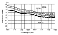
| Isano et al. | Improvement of phase retardation of wave plate with subwavelength structures by heat treatment | |
| JP2004063506A (ja) | 強誘電体膜の加工方法 | |
| JP2001249224A (ja) | 回折格子型偏光素子及びその製造方法 | |
| JPH07225469A (ja) | 露光用マスクおよびその製造方法 | |
| WO2013125933A2 (ru) | Халькогенидный as-se-s электронный резист |
Legal Events
| Date | Code | Title | Description |
|---|---|---|---|
| A521 | Written amendment |
Free format text: JAPANESE INTERMEDIATE CODE: A523 Effective date: 20070222 |
|
| A621 | Written request for application examination |
Free format text: JAPANESE INTERMEDIATE CODE: A621 Effective date: 20070222 |
|
| A977 | Report on retrieval |
Free format text: JAPANESE INTERMEDIATE CODE: A971007 Effective date: 20091106 |
|
| A131 | Notification of reasons for refusal |
Free format text: JAPANESE INTERMEDIATE CODE: A131 Effective date: 20091110 |
|
| A521 | Written amendment |
Free format text: JAPANESE INTERMEDIATE CODE: A523 Effective date: 20091214 |
|
| TRDD | Decision of grant or rejection written | ||
| A01 | Written decision to grant a patent or to grant a registration (utility model) |
Free format text: JAPANESE INTERMEDIATE CODE: A01 Effective date: 20100112 |
|
| A01 | Written decision to grant a patent or to grant a registration (utility model) |
Free format text: JAPANESE INTERMEDIATE CODE: A01 |
|
| A61 | First payment of annual fees (during grant procedure) |
Free format text: JAPANESE INTERMEDIATE CODE: A61 Effective date: 20100114 |
|
| R150 | Certificate of patent or registration of utility model |
Free format text: JAPANESE INTERMEDIATE CODE: R150 |
|
| FPAY | Renewal fee payment (event date is renewal date of database) |
Free format text: PAYMENT UNTIL: 20130122 Year of fee payment: 3 |
|
| FPAY | Renewal fee payment (event date is renewal date of database) |
Free format text: PAYMENT UNTIL: 20140122 Year of fee payment: 4 |
|
| LAPS | Cancellation because of no payment of annual fees |