JP4337574B2 - LIGHT EMITTING DEVICE AND METHOD FOR FORMING THE SAME - Google Patents
LIGHT EMITTING DEVICE AND METHOD FOR FORMING THE SAME Download PDFInfo
- Publication number
- JP4337574B2 JP4337574B2 JP2004037716A JP2004037716A JP4337574B2 JP 4337574 B2 JP4337574 B2 JP 4337574B2 JP 2004037716 A JP2004037716 A JP 2004037716A JP 2004037716 A JP2004037716 A JP 2004037716A JP 4337574 B2 JP4337574 B2 JP 4337574B2
- Authority
- JP
- Japan
- Prior art keywords
- light emitting
- wavelength conversion
- conversion member
- light
- emitting device
- Prior art date
- Legal status (The legal status is an assumption and is not a legal conclusion. Google has not performed a legal analysis and makes no representation as to the accuracy of the status listed.)
- Expired - Fee Related
Links
- 238000000034 method Methods 0.000 title claims description 60
- 238000006243 chemical reaction Methods 0.000 claims description 224
- OAICVXFJPJFONN-UHFFFAOYSA-N Phosphorus Chemical compound [P] OAICVXFJPJFONN-UHFFFAOYSA-N 0.000 claims description 196
- 239000000463 material Substances 0.000 claims description 114
- 239000000203 mixture Substances 0.000 claims description 106
- 239000000758 substrate Substances 0.000 claims description 75
- 239000002245 particle Substances 0.000 claims description 38
- 229910052712 strontium Inorganic materials 0.000 claims description 38
- 229910052791 calcium Inorganic materials 0.000 claims description 32
- 229910052782 aluminium Inorganic materials 0.000 claims description 30
- 238000007789 sealing Methods 0.000 claims description 28
- 229910052761 rare earth metal Inorganic materials 0.000 claims description 20
- 239000000126 substance Substances 0.000 claims description 20
- 229910052727 yttrium Inorganic materials 0.000 claims description 20
- 229910052788 barium Inorganic materials 0.000 claims description 16
- 239000011230 binding agent Substances 0.000 claims description 16
- 229910052749 magnesium Inorganic materials 0.000 claims description 16
- 229910052725 zinc Inorganic materials 0.000 claims description 15
- 229910052710 silicon Inorganic materials 0.000 claims description 12
- 229910052688 Gadolinium Inorganic materials 0.000 claims description 11
- 230000004888 barrier function Effects 0.000 claims description 11
- 229910052771 Terbium Inorganic materials 0.000 claims description 10
- 229910052746 lanthanum Inorganic materials 0.000 claims description 10
- 229910052765 Lutetium Inorganic materials 0.000 claims description 9
- 229910052772 Samarium Inorganic materials 0.000 claims description 8
- 229910052738 indium Inorganic materials 0.000 claims description 6
- 229910052732 germanium Inorganic materials 0.000 claims description 5
- 229910052790 beryllium Inorganic materials 0.000 claims description 4
- 229910052799 carbon Inorganic materials 0.000 claims description 4
- 229910052706 scandium Inorganic materials 0.000 claims description 4
- 229910052718 tin Inorganic materials 0.000 claims description 4
- 229910052719 titanium Inorganic materials 0.000 claims description 3
- 229910052726 zirconium Inorganic materials 0.000 claims description 3
- 229910052735 hafnium Inorganic materials 0.000 claims 1
- 239000010410 layer Substances 0.000 description 69
- 239000011575 calcium Substances 0.000 description 55
- 239000004065 semiconductor Substances 0.000 description 51
- 150000004767 nitrides Chemical class 0.000 description 47
- 229920005989 resin Polymers 0.000 description 41
- 239000011347 resin Substances 0.000 description 41
- 229910052693 Europium Inorganic materials 0.000 description 35
- NJPPVKZQTLUDBO-UHFFFAOYSA-N novaluron Chemical compound C1=C(Cl)C(OC(F)(F)C(OC(F)(F)F)F)=CC=C1NC(=O)NC(=O)C1=C(F)C=CC=C1F NJPPVKZQTLUDBO-UHFFFAOYSA-N 0.000 description 31
- 239000011572 manganese Substances 0.000 description 28
- 229910052751 metal Inorganic materials 0.000 description 28
- 239000002184 metal Substances 0.000 description 28
- 239000002994 raw material Substances 0.000 description 28
- 229910052684 Cerium Inorganic materials 0.000 description 23
- 229920002050 silicone resin Polymers 0.000 description 20
- 239000002223 garnet Substances 0.000 description 18
- -1 nitride compound Chemical class 0.000 description 17
- XAGFODPZIPBFFR-UHFFFAOYSA-N aluminium Chemical compound [Al] XAGFODPZIPBFFR-UHFFFAOYSA-N 0.000 description 16
- 239000012298 atmosphere Substances 0.000 description 16
- 150000001875 compounds Chemical class 0.000 description 16
- 239000010931 gold Substances 0.000 description 14
- 238000002156 mixing Methods 0.000 description 14
- 229910002601 GaN Inorganic materials 0.000 description 12
- 238000001723 curing Methods 0.000 description 12
- 238000010304 firing Methods 0.000 description 12
- 229910052748 manganese Inorganic materials 0.000 description 12
- 229910007991 Si-N Inorganic materials 0.000 description 10
- VYPSYNLAJGMNEJ-UHFFFAOYSA-N Silicium dioxide Chemical compound O=[Si]=O VYPSYNLAJGMNEJ-UHFFFAOYSA-N 0.000 description 10
- 229910006294 Si—N Inorganic materials 0.000 description 10
- 230000015572 biosynthetic process Effects 0.000 description 10
- 230000007423 decrease Effects 0.000 description 10
- 230000005284 excitation Effects 0.000 description 10
- 238000010438 heat treatment Methods 0.000 description 10
- 238000009877 rendering Methods 0.000 description 10
- 229910052594 sapphire Inorganic materials 0.000 description 10
- 239000010980 sapphire Substances 0.000 description 10
- MUBZPKHOEPUJKR-UHFFFAOYSA-N Oxalic acid Chemical compound OC(=O)C(O)=O MUBZPKHOEPUJKR-UHFFFAOYSA-N 0.000 description 9
- 239000003795 chemical substances by application Substances 0.000 description 9
- 238000009826 distribution Methods 0.000 description 9
- 238000004519 manufacturing process Methods 0.000 description 9
- 229910052796 boron Inorganic materials 0.000 description 8
- 230000008859 change Effects 0.000 description 8
- 238000009792 diffusion process Methods 0.000 description 8
- OGPBJKLSAFTDLK-UHFFFAOYSA-N europium atom Chemical compound [Eu] OGPBJKLSAFTDLK-UHFFFAOYSA-N 0.000 description 8
- CNQCVBJFEGMYDW-UHFFFAOYSA-N lawrencium atom Chemical compound [Lr] CNQCVBJFEGMYDW-UHFFFAOYSA-N 0.000 description 8
- 238000007650 screen-printing Methods 0.000 description 8
- VWQVUPCCIRVNHF-UHFFFAOYSA-N yttrium atom Chemical compound [Y] VWQVUPCCIRVNHF-UHFFFAOYSA-N 0.000 description 8
- 229910052784 alkaline earth metal Inorganic materials 0.000 description 7
- GWXLDORMOJMVQZ-UHFFFAOYSA-N cerium Chemical compound [Ce] GWXLDORMOJMVQZ-UHFFFAOYSA-N 0.000 description 7
- PMHQVHHXPFUNSP-UHFFFAOYSA-M copper(1+);methylsulfanylmethane;bromide Chemical compound Br[Cu].CSC PMHQVHHXPFUNSP-UHFFFAOYSA-M 0.000 description 7
- 238000000295 emission spectrum Methods 0.000 description 7
- 239000007789 gas Substances 0.000 description 7
- 230000017525 heat dissipation Effects 0.000 description 7
- 239000012299 nitrogen atmosphere Substances 0.000 description 7
- TWNQGVIAIRXVLR-UHFFFAOYSA-N oxo(oxoalumanyloxy)alumane Chemical compound O=[Al]O[Al]=O TWNQGVIAIRXVLR-UHFFFAOYSA-N 0.000 description 7
- 238000007665 sagging Methods 0.000 description 7
- 229910052777 Praseodymium Inorganic materials 0.000 description 6
- XUIMIQQOPSSXEZ-UHFFFAOYSA-N Silicon Chemical compound [Si] XUIMIQQOPSSXEZ-UHFFFAOYSA-N 0.000 description 6
- 238000000862 absorption spectrum Methods 0.000 description 6
- 229910052915 alkaline earth metal silicate Inorganic materials 0.000 description 6
- 239000003086 colorant Substances 0.000 description 6
- 229910052802 copper Inorganic materials 0.000 description 6
- 239000002019 doping agent Substances 0.000 description 6
- 230000000694 effects Effects 0.000 description 6
- 230000003287 optical effect Effects 0.000 description 6
- 229910052760 oxygen Inorganic materials 0.000 description 6
- 238000004382 potting Methods 0.000 description 6
- 230000008569 process Effects 0.000 description 6
- 238000000518 rheometry Methods 0.000 description 6
- 239000010703 silicon Substances 0.000 description 6
- 229910052581 Si3N4 Inorganic materials 0.000 description 5
- 239000002585 base Substances 0.000 description 5
- 239000000470 constituent Substances 0.000 description 5
- 230000004907 flux Effects 0.000 description 5
- 229910052733 gallium Inorganic materials 0.000 description 5
- 239000007788 liquid Substances 0.000 description 5
- OHSVLFRHMCKCQY-UHFFFAOYSA-N lutetium atom Chemical compound [Lu] OHSVLFRHMCKCQY-UHFFFAOYSA-N 0.000 description 5
- 229910052759 nickel Inorganic materials 0.000 description 5
- 229910018072 Al 2 O 3 Inorganic materials 0.000 description 4
- VTYYLEPIZMXCLO-UHFFFAOYSA-L Calcium carbonate Chemical compound [Ca+2].[O-]C([O-])=O VTYYLEPIZMXCLO-UHFFFAOYSA-L 0.000 description 4
- 229910052779 Neodymium Inorganic materials 0.000 description 4
- UHAQRCJYQAKQEE-UHFFFAOYSA-M [O-2].[OH-].O.[Al+3].P Chemical compound [O-2].[OH-].O.[Al+3].P UHAQRCJYQAKQEE-UHFFFAOYSA-M 0.000 description 4
- 229910052804 chromium Inorganic materials 0.000 description 4
- 238000010586 diagram Methods 0.000 description 4
- 239000003822 epoxy resin Substances 0.000 description 4
- 229910001940 europium oxide Inorganic materials 0.000 description 4
- AEBZCFFCDTZXHP-UHFFFAOYSA-N europium(3+);oxygen(2-) Chemical compound [O-2].[O-2].[O-2].[Eu+3].[Eu+3] AEBZCFFCDTZXHP-UHFFFAOYSA-N 0.000 description 4
- 238000000605 extraction Methods 0.000 description 4
- 229920000647 polyepoxide Polymers 0.000 description 4
- HQVNEWCFYHHQES-UHFFFAOYSA-N silicon nitride Chemical compound N12[Si]34N5[Si]62N3[Si]51N64 HQVNEWCFYHHQES-UHFFFAOYSA-N 0.000 description 4
- 229910052814 silicon oxide Inorganic materials 0.000 description 4
- 229910052709 silver Inorganic materials 0.000 description 4
- 239000007858 starting material Substances 0.000 description 4
- IJGRMHOSHXDMSA-UHFFFAOYSA-N Atomic nitrogen Chemical compound N#N IJGRMHOSHXDMSA-UHFFFAOYSA-N 0.000 description 3
- BVKZGUZCCUSVTD-UHFFFAOYSA-L Carbonate Chemical compound [O-]C([O-])=O BVKZGUZCCUSVTD-UHFFFAOYSA-L 0.000 description 3
- JMASRVWKEDWRBT-UHFFFAOYSA-N Gallium nitride Chemical compound [Ga]#N JMASRVWKEDWRBT-UHFFFAOYSA-N 0.000 description 3
- BQCADISMDOOEFD-UHFFFAOYSA-N Silver Chemical compound [Ag] BQCADISMDOOEFD-UHFFFAOYSA-N 0.000 description 3
- 229910052769 Ytterbium Inorganic materials 0.000 description 3
- WAAQUBJIWXTCPY-UHFFFAOYSA-N [O-2].[Al+3].P.[Y+3] Chemical compound [O-2].[Al+3].P.[Y+3] WAAQUBJIWXTCPY-UHFFFAOYSA-N 0.000 description 3
- 238000010521 absorption reaction Methods 0.000 description 3
- 239000002253 acid Substances 0.000 description 3
- 239000012190 activator Substances 0.000 description 3
- 229910045601 alloy Inorganic materials 0.000 description 3
- 239000000956 alloy Substances 0.000 description 3
- 239000007864 aqueous solution Substances 0.000 description 3
- 239000012300 argon atmosphere Substances 0.000 description 3
- QVGXLLKOCUKJST-UHFFFAOYSA-N atomic oxygen Chemical compound [O] QVGXLLKOCUKJST-UHFFFAOYSA-N 0.000 description 3
- QVQLCTNNEUAWMS-UHFFFAOYSA-N barium oxide Chemical compound [Ba]=O QVQLCTNNEUAWMS-UHFFFAOYSA-N 0.000 description 3
- 238000005520 cutting process Methods 0.000 description 3
- 239000010408 film Substances 0.000 description 3
- 239000011521 glass Substances 0.000 description 3
- 229910052737 gold Inorganic materials 0.000 description 3
- 230000031700 light absorption Effects 0.000 description 3
- 239000007791 liquid phase Substances 0.000 description 3
- 235000006408 oxalic acid Nutrition 0.000 description 3
- 239000001301 oxygen Substances 0.000 description 3
- 229910052698 phosphorus Inorganic materials 0.000 description 3
- 239000000843 powder Substances 0.000 description 3
- 238000010298 pulverizing process Methods 0.000 description 3
- 229910052703 rhodium Inorganic materials 0.000 description 3
- 239000000377 silicon dioxide Substances 0.000 description 3
- 239000000243 solution Substances 0.000 description 3
- 238000004544 sputter deposition Methods 0.000 description 3
- 229920001187 thermosetting polymer Polymers 0.000 description 3
- QGZKDVFQNNGYKY-UHFFFAOYSA-N Ammonia Chemical compound N QGZKDVFQNNGYKY-UHFFFAOYSA-N 0.000 description 2
- NLXLAEXVIDQMFP-UHFFFAOYSA-N Ammonia chloride Chemical compound [NH4+].[Cl-] NLXLAEXVIDQMFP-UHFFFAOYSA-N 0.000 description 2
- PZNSFCLAULLKQX-UHFFFAOYSA-N Boron nitride Chemical compound N#B PZNSFCLAULLKQX-UHFFFAOYSA-N 0.000 description 2
- 229910052692 Dysprosium Inorganic materials 0.000 description 2
- 229910052691 Erbium Inorganic materials 0.000 description 2
- KRHYYFGTRYWZRS-UHFFFAOYSA-M Fluoride anion Chemical compound [F-] KRHYYFGTRYWZRS-UHFFFAOYSA-M 0.000 description 2
- GYHNNYVSQQEPJS-UHFFFAOYSA-N Gallium Chemical compound [Ga] GYHNNYVSQQEPJS-UHFFFAOYSA-N 0.000 description 2
- 229910052689 Holmium Inorganic materials 0.000 description 2
- UFHFLCQGNIYNRP-UHFFFAOYSA-N Hydrogen Chemical compound [H][H] UFHFLCQGNIYNRP-UHFFFAOYSA-N 0.000 description 2
- PWHULOQIROXLJO-UHFFFAOYSA-N Manganese Chemical compound [Mn] PWHULOQIROXLJO-UHFFFAOYSA-N 0.000 description 2
- 229910019018 Mg 2 Si Inorganic materials 0.000 description 2
- 229910017639 MgSi Inorganic materials 0.000 description 2
- 229910004298 SiO 2 Inorganic materials 0.000 description 2
- 229910006360 Si—O—N Inorganic materials 0.000 description 2
- 229910004122 SrSi Inorganic materials 0.000 description 2
- 229910052775 Thulium Inorganic materials 0.000 description 2
- 150000004703 alkoxides Chemical class 0.000 description 2
- PSBUJOCDKOWAGJ-UHFFFAOYSA-N azanylidyneeuropium Chemical compound [Eu]#N PSBUJOCDKOWAGJ-UHFFFAOYSA-N 0.000 description 2
- 229910002113 barium titanate Inorganic materials 0.000 description 2
- JRPBQTZRNDNNOP-UHFFFAOYSA-N barium titanate Chemical compound [Ba+2].[Ba+2].[O-][Ti]([O-])([O-])[O-] JRPBQTZRNDNNOP-UHFFFAOYSA-N 0.000 description 2
- 230000008901 benefit Effects 0.000 description 2
- 238000001354 calcination Methods 0.000 description 2
- 229910000019 calcium carbonate Inorganic materials 0.000 description 2
- 238000005253 cladding Methods 0.000 description 2
- 238000000975 co-precipitation Methods 0.000 description 2
- 230000003081 coactivator Effects 0.000 description 2
- 239000011248 coating agent Substances 0.000 description 2
- 238000000576 coating method Methods 0.000 description 2
- 230000000052 comparative effect Effects 0.000 description 2
- 230000000295 complement effect Effects 0.000 description 2
- 239000013078 crystal Substances 0.000 description 2
- 238000005530 etching Methods 0.000 description 2
- 238000011049 filling Methods 0.000 description 2
- 239000001257 hydrogen Substances 0.000 description 2
- 229910052739 hydrogen Inorganic materials 0.000 description 2
- XLYOFNOQVPJJNP-UHFFFAOYSA-M hydroxide Chemical compound [OH-] XLYOFNOQVPJJNP-UHFFFAOYSA-M 0.000 description 2
- AMWRITDGCCNYAT-UHFFFAOYSA-L hydroxy(oxo)manganese;manganese Chemical compound [Mn].O[Mn]=O.O[Mn]=O AMWRITDGCCNYAT-UHFFFAOYSA-L 0.000 description 2
- 150000003949 imides Chemical class 0.000 description 2
- 239000012535 impurity Substances 0.000 description 2
- APFVFJFRJDLVQX-UHFFFAOYSA-N indium atom Chemical compound [In] APFVFJFRJDLVQX-UHFFFAOYSA-N 0.000 description 2
- 229910010272 inorganic material Inorganic materials 0.000 description 2
- 239000011147 inorganic material Substances 0.000 description 2
- 238000005304 joining Methods 0.000 description 2
- 238000010030 laminating Methods 0.000 description 2
- 239000007769 metal material Substances 0.000 description 2
- 238000000465 moulding Methods 0.000 description 2
- 229910052757 nitrogen Inorganic materials 0.000 description 2
- 239000012071 phase Substances 0.000 description 2
- 239000000049 pigment Substances 0.000 description 2
- 235000012239 silicon dioxide Nutrition 0.000 description 2
- 239000004332 silver Substances 0.000 description 2
- 239000002356 single layer Substances 0.000 description 2
- 229910000679 solder Inorganic materials 0.000 description 2
- 238000003980 solgel method Methods 0.000 description 2
- 230000035882 stress Effects 0.000 description 2
- 230000008646 thermal stress Effects 0.000 description 2
- 239000010409 thin film Substances 0.000 description 2
- 230000009974 thixotropic effect Effects 0.000 description 2
- 239000010936 titanium Substances 0.000 description 2
- XCZXGTMEAKBVPV-UHFFFAOYSA-N trimethylgallium Chemical compound C[Ga](C)C XCZXGTMEAKBVPV-UHFFFAOYSA-N 0.000 description 2
- IBEFSUTVZWZJEL-UHFFFAOYSA-N trimethylindium Chemical compound C[In](C)C IBEFSUTVZWZJEL-UHFFFAOYSA-N 0.000 description 2
- 229910052720 vanadium Inorganic materials 0.000 description 2
- XLYOFNOQVPJJNP-UHFFFAOYSA-N water Substances O XLYOFNOQVPJJNP-UHFFFAOYSA-N 0.000 description 2
- DDFHBQSCUXNBSA-UHFFFAOYSA-N 5-(5-carboxythiophen-2-yl)thiophene-2-carboxylic acid Chemical compound S1C(C(=O)O)=CC=C1C1=CC=C(C(O)=O)S1 DDFHBQSCUXNBSA-UHFFFAOYSA-N 0.000 description 1
- 229920000178 Acrylic resin Polymers 0.000 description 1
- 239000004925 Acrylic resin Substances 0.000 description 1
- 229910002704 AlGaN Inorganic materials 0.000 description 1
- 229910015363 Au—Sn Inorganic materials 0.000 description 1
- 229910052582 BN Inorganic materials 0.000 description 1
- 229910016066 BaSi Inorganic materials 0.000 description 1
- 230000005457 Black-body radiation Effects 0.000 description 1
- BTBUEUYNUDRHOZ-UHFFFAOYSA-N Borate Chemical compound [O-]B([O-])[O-] BTBUEUYNUDRHOZ-UHFFFAOYSA-N 0.000 description 1
- ZOXJGFHDIHLPTG-UHFFFAOYSA-N Boron Chemical group [B] ZOXJGFHDIHLPTG-UHFFFAOYSA-N 0.000 description 1
- 229910004709 CaSi Inorganic materials 0.000 description 1
- 229910020314 ClBr Inorganic materials 0.000 description 1
- 239000004606 Fillers/Extenders Substances 0.000 description 1
- 229910005793 GeO 2 Inorganic materials 0.000 description 1
- 229910052766 Lawrencium Inorganic materials 0.000 description 1
- 229910020220 Pb—Sn Inorganic materials 0.000 description 1
- 206010037660 Pyrexia Diseases 0.000 description 1
- 229910008048 Si-S Inorganic materials 0.000 description 1
- 229910006336 Si—S Inorganic materials 0.000 description 1
- 229910020816 Sn Pb Inorganic materials 0.000 description 1
- 229910020922 Sn-Pb Inorganic materials 0.000 description 1
- 229910008783 Sn—Pb Inorganic materials 0.000 description 1
- 229910003668 SrAl Inorganic materials 0.000 description 1
- ATJFFYVFTNAWJD-UHFFFAOYSA-N Tin Chemical compound [Sn] ATJFFYVFTNAWJD-UHFFFAOYSA-N 0.000 description 1
- GWEVSGVZZGPLCZ-UHFFFAOYSA-N Titan oxide Chemical compound O=[Ti]=O GWEVSGVZZGPLCZ-UHFFFAOYSA-N 0.000 description 1
- 229920001807 Urea-formaldehyde Polymers 0.000 description 1
- 229910001361 White metal Inorganic materials 0.000 description 1
- UAHZTKVCYHJBJQ-UHFFFAOYSA-N [P].S=O Chemical compound [P].S=O UAHZTKVCYHJBJQ-UHFFFAOYSA-N 0.000 description 1
- NIXOWILDQLNWCW-UHFFFAOYSA-N acrylic acid group Chemical group C(C=C)(=O)O NIXOWILDQLNWCW-UHFFFAOYSA-N 0.000 description 1
- 239000000654 additive Substances 0.000 description 1
- 230000000996 additive effect Effects 0.000 description 1
- 230000002411 adverse Effects 0.000 description 1
- 239000003513 alkali Substances 0.000 description 1
- 150000004645 aluminates Chemical class 0.000 description 1
- PNEYBMLMFCGWSK-UHFFFAOYSA-N aluminium oxide Inorganic materials [O-2].[O-2].[O-2].[Al+3].[Al+3] PNEYBMLMFCGWSK-UHFFFAOYSA-N 0.000 description 1
- JNDMLEXHDPKVFC-UHFFFAOYSA-N aluminum;oxygen(2-);yttrium(3+) Chemical compound [O-2].[O-2].[O-2].[Al+3].[Y+3] JNDMLEXHDPKVFC-UHFFFAOYSA-N 0.000 description 1
- 150000001408 amides Chemical class 0.000 description 1
- 229910021529 ammonia Inorganic materials 0.000 description 1
- 235000019270 ammonium chloride Nutrition 0.000 description 1
- 229910052787 antimony Inorganic materials 0.000 description 1
- 229910052586 apatite Inorganic materials 0.000 description 1
- 229910052789 astatine Inorganic materials 0.000 description 1
- 238000000498 ball milling Methods 0.000 description 1
- OYLGJCQECKOTOL-UHFFFAOYSA-L barium fluoride Chemical compound [F-].[F-].[Ba+2] OYLGJCQECKOTOL-UHFFFAOYSA-L 0.000 description 1
- 229910001632 barium fluoride Inorganic materials 0.000 description 1
- 230000005540 biological transmission Effects 0.000 description 1
- 229910052794 bromium Inorganic materials 0.000 description 1
- 229910052793 cadmium Inorganic materials 0.000 description 1
- ODINCKMPIJJUCX-UHFFFAOYSA-N calcium oxide Inorganic materials [Ca]=O ODINCKMPIJJUCX-UHFFFAOYSA-N 0.000 description 1
- 125000005587 carbonate group Chemical group 0.000 description 1
- 239000012159 carrier gas Substances 0.000 description 1
- 229910052801 chlorine Inorganic materials 0.000 description 1
- 239000002131 composite material Substances 0.000 description 1
- 238000001816 cooling Methods 0.000 description 1
- 239000011258 core-shell material Substances 0.000 description 1
- 230000003247 decreasing effect Effects 0.000 description 1
- 238000000151 deposition Methods 0.000 description 1
- 230000006866 deterioration Effects 0.000 description 1
- AJNVQOSZGJRYEI-UHFFFAOYSA-N digallium;oxygen(2-) Chemical compound [O-2].[O-2].[O-2].[Ga+3].[Ga+3] AJNVQOSZGJRYEI-UHFFFAOYSA-N 0.000 description 1
- 229910001873 dinitrogen Inorganic materials 0.000 description 1
- 239000006185 dispersion Substances 0.000 description 1
- 238000001035 drying Methods 0.000 description 1
- 230000005496 eutectics Effects 0.000 description 1
- 238000000695 excitation spectrum Methods 0.000 description 1
- 230000002349 favourable effect Effects 0.000 description 1
- 239000000945 filler Substances 0.000 description 1
- 239000010419 fine particle Substances 0.000 description 1
- 239000012530 fluid Substances 0.000 description 1
- 150000002259 gallium compounds Chemical class 0.000 description 1
- 229910001195 gallium oxide Inorganic materials 0.000 description 1
- GNPVGFCGXDBREM-UHFFFAOYSA-N germanium atom Chemical group [Ge] GNPVGFCGXDBREM-UHFFFAOYSA-N 0.000 description 1
- PCHJSUWPFVWCPO-UHFFFAOYSA-N gold Chemical compound [Au] PCHJSUWPFVWCPO-UHFFFAOYSA-N 0.000 description 1
- 230000005484 gravity Effects 0.000 description 1
- 150000004820 halides Chemical class 0.000 description 1
- 229910052736 halogen Inorganic materials 0.000 description 1
- 150000002367 halogens Chemical class 0.000 description 1
- 238000013007 heat curing Methods 0.000 description 1
- 230000020169 heat generation Effects 0.000 description 1
- 125000005842 heteroatom Chemical group 0.000 description 1
- 230000006872 improvement Effects 0.000 description 1
- 239000011261 inert gas Substances 0.000 description 1
- 238000001746 injection moulding Methods 0.000 description 1
- 150000002500 ions Chemical class 0.000 description 1
- 229910052741 iridium Inorganic materials 0.000 description 1
- 229910052742 iron Inorganic materials 0.000 description 1
- MRELNEQAGSRDBK-UHFFFAOYSA-N lanthanum(3+);oxygen(2-) Chemical compound [O-2].[O-2].[O-2].[La+3].[La+3] MRELNEQAGSRDBK-UHFFFAOYSA-N 0.000 description 1
- 238000007561 laser diffraction method Methods 0.000 description 1
- RYZCLUQMCYZBJQ-UHFFFAOYSA-H lead(2+);dicarbonate;dihydroxide Chemical group [OH-].[OH-].[Pb+2].[Pb+2].[Pb+2].[O-]C([O-])=O.[O-]C([O-])=O RYZCLUQMCYZBJQ-UHFFFAOYSA-H 0.000 description 1
- 229910052744 lithium Inorganic materials 0.000 description 1
- 230000007774 longterm Effects 0.000 description 1
- 150000002663 lutetium compounds Chemical class 0.000 description 1
- WPBNNNQJVZRUHP-UHFFFAOYSA-L manganese(2+);methyl n-[[2-(methoxycarbonylcarbamothioylamino)phenyl]carbamothioyl]carbamate;n-[2-(sulfidocarbothioylamino)ethyl]carbamodithioate Chemical compound [Mn+2].[S-]C(=S)NCCNC([S-])=S.COC(=O)NC(=S)NC1=CC=CC=C1NC(=S)NC(=O)OC WPBNNNQJVZRUHP-UHFFFAOYSA-L 0.000 description 1
- VASIZKWUTCETSD-UHFFFAOYSA-N manganese(II) oxide Inorganic materials [Mn]=O VASIZKWUTCETSD-UHFFFAOYSA-N 0.000 description 1
- 229910052914 metal silicate Inorganic materials 0.000 description 1
- 238000002488 metal-organic chemical vapour deposition Methods 0.000 description 1
- 150000002739 metals Chemical class 0.000 description 1
- 229910003465 moissanite Inorganic materials 0.000 description 1
- 229910052750 molybdenum Inorganic materials 0.000 description 1
- 239000011368 organic material Substances 0.000 description 1
- UHTYDNCIXKPJDA-UHFFFAOYSA-H oxalate;praseodymium(3+) Chemical compound [Pr+3].[Pr+3].[O-]C(=O)C([O-])=O.[O-]C(=O)C([O-])=O.[O-]C(=O)C([O-])=O UHTYDNCIXKPJDA-UHFFFAOYSA-H 0.000 description 1
- MMKQUGHLEMYQSG-UHFFFAOYSA-N oxygen(2-);praseodymium(3+) Chemical compound [O-2].[O-2].[O-2].[Pr+3].[Pr+3] MMKQUGHLEMYQSG-UHFFFAOYSA-N 0.000 description 1
- 230000000149 penetrating effect Effects 0.000 description 1
- VSIIXMUUUJUKCM-UHFFFAOYSA-D pentacalcium;fluoride;triphosphate Chemical compound [F-].[Ca+2].[Ca+2].[Ca+2].[Ca+2].[Ca+2].[O-]P([O-])([O-])=O.[O-]P([O-])([O-])=O.[O-]P([O-])([O-])=O VSIIXMUUUJUKCM-UHFFFAOYSA-D 0.000 description 1
- 230000035699 permeability Effects 0.000 description 1
- 239000011574 phosphorus Chemical group 0.000 description 1
- 230000000704 physical effect Effects 0.000 description 1
- 238000007747 plating Methods 0.000 description 1
- 229910052697 platinum Inorganic materials 0.000 description 1
- 229910052700 potassium Inorganic materials 0.000 description 1
- 150000003114 praseodymium compounds Chemical class 0.000 description 1
- 229910003447 praseodymium oxide Inorganic materials 0.000 description 1
- 238000003825 pressing Methods 0.000 description 1
- 238000007639 printing Methods 0.000 description 1
- 238000010791 quenching Methods 0.000 description 1
- 230000000171 quenching effect Effects 0.000 description 1
- 230000005855 radiation Effects 0.000 description 1
- 229910001404 rare earth metal oxide Inorganic materials 0.000 description 1
- 150000002910 rare earth metals Chemical class 0.000 description 1
- 239000011342 resin composition Substances 0.000 description 1
- 230000002441 reversible effect Effects 0.000 description 1
- 229910052702 rhenium Inorganic materials 0.000 description 1
- 238000000790 scattering method Methods 0.000 description 1
- 238000004062 sedimentation Methods 0.000 description 1
- 229910052711 selenium Inorganic materials 0.000 description 1
- SBIBMFFZSBJNJF-UHFFFAOYSA-N selenium;zinc Chemical compound [Se]=[Zn] SBIBMFFZSBJNJF-UHFFFAOYSA-N 0.000 description 1
- 238000004904 shortening Methods 0.000 description 1
- 229910010271 silicon carbide Inorganic materials 0.000 description 1
- 229910052708 sodium Inorganic materials 0.000 description 1
- 239000011734 sodium Substances 0.000 description 1
- GCLGEJMYGQKIIW-UHFFFAOYSA-H sodium hexametaphosphate Chemical compound [Na]OP1(=O)OP(=O)(O[Na])OP(=O)(O[Na])OP(=O)(O[Na])OP(=O)(O[Na])OP(=O)(O[Na])O1 GCLGEJMYGQKIIW-UHFFFAOYSA-H 0.000 description 1
- 235000019982 sodium hexametaphosphate Nutrition 0.000 description 1
- 239000007787 solid Substances 0.000 description 1
- 229910052596 spinel Inorganic materials 0.000 description 1
- 239000011029 spinel Substances 0.000 description 1
- 238000003892 spreading Methods 0.000 description 1
- 230000007480 spreading Effects 0.000 description 1
- 238000006467 substitution reaction Methods 0.000 description 1
- 239000000725 suspension Substances 0.000 description 1
- 230000002194 synthesizing effect Effects 0.000 description 1
- 229910052714 tellurium Inorganic materials 0.000 description 1
- 239000001577 tetrasodium phosphonato phosphate Substances 0.000 description 1
- 238000005979 thermal decomposition reaction Methods 0.000 description 1
- OGIDPMRJRNCKJF-UHFFFAOYSA-N titanium oxide Inorganic materials [Ti]=O OGIDPMRJRNCKJF-UHFFFAOYSA-N 0.000 description 1
- 229910052721 tungsten Inorganic materials 0.000 description 1
- 238000007740 vapor deposition Methods 0.000 description 1
- 238000005406 washing Methods 0.000 description 1
- 239000010969 white metal Substances 0.000 description 1
Images


Classifications
-
- H—ELECTRICITY
- H01—ELECTRIC ELEMENTS
- H01L—SEMICONDUCTOR DEVICES NOT COVERED BY CLASS H10
- H01L2224/00—Indexing scheme for arrangements for connecting or disconnecting semiconductor or solid-state bodies and methods related thereto as covered by H01L24/00
- H01L2224/01—Means for bonding being attached to, or being formed on, the surface to be connected, e.g. chip-to-package, die-attach, "first-level" interconnects; Manufacturing methods related thereto
- H01L2224/10—Bump connectors; Manufacturing methods related thereto
- H01L2224/15—Structure, shape, material or disposition of the bump connectors after the connecting process
- H01L2224/16—Structure, shape, material or disposition of the bump connectors after the connecting process of an individual bump connector
- H01L2224/161—Disposition
- H01L2224/16151—Disposition the bump connector connecting between a semiconductor or solid-state body and an item not being a semiconductor or solid-state body, e.g. chip-to-substrate, chip-to-passive
- H01L2224/16221—Disposition the bump connector connecting between a semiconductor or solid-state body and an item not being a semiconductor or solid-state body, e.g. chip-to-substrate, chip-to-passive the body and the item being stacked
- H01L2224/16225—Disposition the bump connector connecting between a semiconductor or solid-state body and an item not being a semiconductor or solid-state body, e.g. chip-to-substrate, chip-to-passive the body and the item being stacked the item being non-metallic, e.g. insulating substrate with or without metallisation
Description
本発明は、発光素子と蛍光物質とを利用した発光装置、およびその製造方法に関わり、特に発光効率が高く、発光観測方位によって色度ズレが少なく光学特性に優れ、信頼性の高い発光装置およびその製造方法を提供することを目的とする。 The present invention relates to a light-emitting device using a light-emitting element and a fluorescent material, and a method for manufacturing the light-emitting device, and particularly to a light-emitting device that has high emission efficiency, little chromaticity deviation depending on the emission observation direction, excellent optical characteristics, and high reliability. It aims at providing the manufacturing method.
近年、発光素子と、発光素子からの光の少なくとも一部を吸収して異なる波長を有する光を発光する蛍光物質とを組み合わせた発光装置が製品化されている。例えば、特開平11−40848号公報や特開2001−15817号公報に開示される発光装置は、支持基板にフリップチップ実装された発光素子の周辺に、蛍光体を含有する樹脂の層がディペンサーを利用したポッティングやスクリーン印刷にて配置されて形成されている。 In recent years, light-emitting devices that combine a light-emitting element and a fluorescent material that emits light having different wavelengths by absorbing at least part of the light from the light-emitting element have been commercialized. For example, in a light emitting device disclosed in Japanese Patent Application Laid-Open No. 11-40848 and Japanese Patent Application Laid-Open No. 2001-15817, a resin layer containing a phosphor has a dispenser around a light emitting element flip-chip mounted on a support substrate. It is arranged and formed by using potting or screen printing.
しかしながら、ディペンサーを利用したポッティングによる波長変換部材の形成方法は、蛍光体含有の液状樹脂を供給し、波長変換部材を形成するときに、液状樹脂のレオロジーにより波長変換部材の表面が曲面となってしまい、発光素子の周辺で均一な層厚の波長変換部材が形成されない。また、スクリーン印刷による波長変換部材の形成方法も同様に、液状樹脂のレオロジーにより発光素子の側面側において波長変換部材の表面が曲面となってしまい、均一な層厚の波長変換部材が形成されない。したがって、発光素子からの光と、その光が蛍光体により波長変換された光との混色光の色温度が各発光観測方位によって異なり、色度ズレが少なく信頼性の高い発光装置とすることができない。 However, in the method of forming a wavelength conversion member by potting using a dispenser, when the phosphor-containing liquid resin is supplied and the wavelength conversion member is formed, the surface of the wavelength conversion member becomes a curved surface due to the rheology of the liquid resin. Therefore, a wavelength conversion member having a uniform layer thickness is not formed around the light emitting element. Similarly, in the method of forming the wavelength conversion member by screen printing, the surface of the wavelength conversion member becomes a curved surface on the side surface side of the light emitting element due to the rheology of the liquid resin, and the wavelength conversion member having a uniform layer thickness is not formed. Therefore, the color temperature of the mixed color light of the light from the light emitting element and the light whose wavelength is converted by the phosphor varies depending on each light emission observation direction, and the light emitting device has a low chromaticity shift and high reliability. Can not.
また、発光素子の電極が導電パターンにバンプを介して接合された発光装置において、発光素子からの放熱は主にバンプを介してサブマウントの方向へ行われることとなり、バンプの周辺およびサブマウントが発熱する。一般に、蛍光体は蛍光体の周囲温度の上昇と共に発光輝度が低下する傾向にある。従って、バンプの周辺に蛍光体を配置すると、発光装置の発光効率が低下する。 In the light emitting device in which the electrode of the light emitting element is bonded to the conductive pattern via the bump, the heat radiation from the light emitting element is mainly performed in the direction of the submount via the bump. Fever. In general, phosphors tend to have lower emission luminance as the ambient temperature of the phosphor increases. Therefore, if the phosphor is disposed around the bump, the light emission efficiency of the light emitting device is lowered.
そこで、本発明は、発光観測方位によって混色光の色温度が異なることなく、発光効率が高い発光装置およびその形成方法を提供することを目的とする。 Therefore, an object of the present invention is to provide a light emitting device having high light emission efficiency and a method for forming the same without causing the color temperature of mixed color light to vary depending on the light emission observation direction.
以上の目的を達成するために本発明に係る発光装置は、電極が導電部材を介して支持基板の導電パターンに対向し接合されている発光素子と、該発光素子の光の少なくとも一部を吸収して異なる波長を有する光を発する蛍光物質を含有し前記発光素子の少なくとも一部を被覆する波長変換部材とを有する発光装置において、上記波長変換部材は、上記導電部材から離間されていることを特徴とする。さらに、上記波長変換部材は、上記支持基板から少なくとも部分的に離間されている。また、波長変換部材は、導電部材または支持基板から樹脂を含む部材、例えばアンダーフィル材を介して離間されていることが好ましい。このように構成すると、蛍光体の輝度が周囲温度の上昇と共に低下することを抑制することができるため、従来技術と比較して発光効率の高い発光装置とすることができる。また、従来技術と比較して発光観測方位によって層厚が均一の波長変換部材を有するため、発光観測方位によって色温度がほぼ同じの発光装置とすることができる。 In order to achieve the above object, a light emitting device according to the present invention absorbs at least a part of light of a light emitting element in which an electrode is opposed to and bonded to a conductive pattern of a support substrate via a conductive member. And a wavelength conversion member that includes a fluorescent material that emits light having different wavelengths and covers at least a part of the light emitting element, wherein the wavelength conversion member is separated from the conductive member. Features. Further, the wavelength conversion member is at least partially separated from the support substrate. Moreover, it is preferable that the wavelength conversion member is separated from the conductive member or the support substrate via a member containing resin, for example, an underfill material. If comprised in this way, since it can suppress that the brightness | luminance of fluorescent substance falls with the raise of ambient temperature, it can be set as the light-emitting device with high luminous efficiency compared with a prior art. In addition, since the wavelength conversion member having a uniform layer thickness according to the emission observation direction is provided as compared with the prior art, a light emitting device having substantially the same color temperature according to the emission observation direction can be obtained.
また、上記波長変換部材は、上記発光素子の側面方向に配置される第一の波長変換部材と、上記発光素子の発光観測面側主面を被覆する第二の波長変換部材とからなり、上記第一の波長変換部材は、上記発光観測面側主面を含む平面から突出する上端部を有し、上記第二の波長変換部材は、上記上端部の少なくとも一部を被覆することが好ましい。また、第二の波長変換部材は、上記発光素子の側面と上記第一の波長変換部材との間に介在していることが好ましい。このように構成すると、発光観測方位によって色温度がほぼ同じの発光装置とし、第二の波長変換部材を発光素子の発光観測面側主面方向にて強固に固定保持することができるため、信頼性の高い発光装置とすることができる。 The wavelength conversion member includes a first wavelength conversion member disposed in a side surface direction of the light emitting element and a second wavelength conversion member covering the light emission observation surface side main surface of the light emitting element. Preferably, the first wavelength conversion member has an upper end portion protruding from a plane including the emission observation surface side main surface, and the second wavelength conversion member covers at least a part of the upper end portion. Moreover, it is preferable that the 2nd wavelength conversion member is interposed between the side surface of the said light emitting element, and said 1st wavelength conversion member. This configuration makes it possible to obtain a light emitting device having substantially the same color temperature depending on the light emission observation direction, and the second wavelength conversion member can be firmly fixed and held in the direction of the main light emission surface side of the light emitting element. A highly light-emitting device can be obtained.
また、上記第一の波長変換部材は、上記第二の波長変換部材の発光観測面側主面を含む平面から突出する上端部を有し、上記第二の波長変換部材が該上端部により位置決めされる封止部材を有する。このように構成すると、封止部材を発光素子の主面方向にて固定保持することができるため、信頼性の高い発光装置とすることができる。 Further, the first wavelength conversion member has an upper end portion protruding from a plane including the main surface on the light emission observation surface side of the second wavelength conversion member, and the second wavelength conversion member is positioned by the upper end portion. Having a sealing member. If comprised in this way, since a sealing member can be fixedly held in the main surface direction of a light emitting element, it can be set as a reliable light-emitting device.
また、蛍光物質は、AlとY、Lu、Sc、La、Gd、Tb、Eu、Ga、In及びSmから選択された少なくとも一つの元素とを含み、かつ希土類元素から選択された少なくとも一つの元素で付活された蛍光体、および、Nを含み、かつBe、Mg、Ca、Sr、Ba、及びZnから選択された少なくとも一つの元素と、C、Si、Ge、Sn、Ti、Zr、及びHfから選択された少なくとも一つの元素とを含み、希土類元素から選択された少なくとも一つの元素で付活された蛍光体から選択された少なくとも一種の蛍光体である。これにより、本発明にかかる発光装置は、発光素子からの光と、発光素子からの光の少なくとも一部が蛍光物質により吸収され異なる波長を有する光との混色光を発光することができる。また、二種以上の蛍光体を組み合わせることにより混色光の演色性を向上させることができる。さらに、第二の波長変換部材に含有される粒子状蛍光物質の中心粒径は、第一の波長変換部材に含有される粒子状蛍光物質の中心粒径より大きい。これにより、波長変換部材中の蛍光体分布を均一とし、発光輝度が高く発光観測方位によって色度が均一な発光装置とすることができる。 The fluorescent material includes Al and at least one element selected from Y, Lu, Sc, La, Gd, Tb, Eu, Ga, In and Sm, and at least one element selected from rare earth elements. And at least one element selected from Be, Mg, Ca, Sr, Ba, and Zn, and C, Si, Ge, Sn, Ti, Zr, and It is at least one phosphor selected from phosphors including at least one element selected from Hf and activated by at least one element selected from rare earth elements. As a result, the light emitting device according to the present invention can emit mixed color light of light from the light emitting element and light having different wavelengths in which at least part of the light from the light emitting element is absorbed by the fluorescent material. In addition, the color rendering properties of mixed color light can be improved by combining two or more kinds of phosphors. Furthermore, the center particle size of the particulate fluorescent material contained in the second wavelength conversion member is larger than the center particle size of the particulate fluorescent material contained in the first wavelength conversion member. Thereby, the phosphor distribution in the wavelength conversion member can be made uniform, and the light emitting device having high emission luminance and uniform chromaticity according to the emission observation direction can be obtained.
さらに、以上の目的を達成するために本発明に係る発光装置の形成方法は、発光素子と、該発光素子からの光の少なくとも一部を吸収して異なる波長を有する光を発光する蛍光物質を含有する波長変換部材とを有する発光装置の形成方法において、蛍光物質と該蛍光物質を固着させる結着剤との混合物を上記発光素子の外周に沿うように供給する第一の工程と、上記混合物を障壁として位置決めし、上記発光素子の主面側に蛍光物質と結着剤との混合物を供給する第二の工程と、上記混合物のうち少なくとも一方を硬化させる第三の工程とを含むことを特徴とする。このように構成すると、従来技術と比較して発光観測方位によって色温度がほぼ同じ発光装置を容易に形成することができる。 Furthermore, in order to achieve the above object, a method for forming a light-emitting device according to the present invention includes a light-emitting element and a phosphor that emits light having different wavelengths by absorbing at least part of light from the light-emitting element. In a method for forming a light emitting device having a wavelength conversion member, a first step of supplying a mixture of a fluorescent material and a binder for fixing the fluorescent material along the outer periphery of the light emitting element, and the mixture A second step of supplying a mixture of a fluorescent material and a binder to the main surface side of the light emitting element, and a third step of curing at least one of the mixture. Features. With this configuration, it is possible to easily form a light emitting device having substantially the same color temperature depending on the light emission observation direction as compared with the prior art.
また、第一の工程により供給された混合物は、第二の工程の前に硬化されることが好ましい。このように構成すると、硬化された第一の波長変換部材を障壁として第二の波長変換部材の材料を位置決めすることが容易にできる。 Moreover, it is preferable that the mixture supplied by the 1st process is hardened | cured before a 2nd process. If comprised in this way, the material of the 2nd wavelength conversion member can be easily positioned by making the hardened 1st wavelength conversion member into a barrier.
また、第一の工程の前に、発光素子の電極が導電部材を介して支持基板の導電パターンに接合される。このように、フリップチップ実装において、バンプのような導電部材から離間させて波長変換部材を形成することにより、従来技術と比較して放熱性を向上させ発光効率の高い発光装置をとすることが容易にできる。 Further, before the first step, the electrode of the light emitting element is bonded to the conductive pattern of the support substrate via the conductive member. As described above, in the flip-chip mounting, by forming the wavelength conversion member away from the conductive member such as the bump, it is possible to improve the heat dissipation and make the light emitting device with high light emission efficiency as compared with the prior art. Easy to do.
また、本発明は、第二の工程により供給される混合物中の粒子状蛍光物質の中心粒径が、第一の工程により供給される混合物中の粒子状蛍光物質の中心粒径より大きくすることができる。これにより、発光輝度が高く発光観測方位によって色度が均一な発光装置を形成することが容易にできる。 In the present invention, the center particle size of the particulate fluorescent material in the mixture supplied in the second step is larger than the center particle size of the particulate fluorescent material in the mixture supplied in the first step. Can do. Thereby, it is possible to easily form a light emitting device having high light emission luminance and uniform chromaticity according to the light emission observation direction.
本発明にかかる発光装置は、周囲温度の上昇による発光効率の低下を抑え、発光観測方位によって混色光の色温度が異なることがない。また、本発明にかかる形成方法によれば、発光観測方位によって混色光の色温度や色度が異なることがない発光装置を容易に形成することができる。 The light emitting device according to the present invention suppresses a decrease in light emission efficiency due to an increase in ambient temperature, and the color temperature of the mixed color light does not vary depending on the light emission observation direction. Further, according to the forming method of the present invention, it is possible to easily form a light emitting device in which the color temperature or chromaticity of the mixed color light does not differ depending on the emission observation direction.
本発明を実施するための最良の形態を、以下に図面を参照しながら説明する。ただし、以下に示す形態は、本発明の技術思想を具体化するための発光装置およびその形成方法を例示するものであって、本発明は発光装置およびその形成方法を以下に限定するものではない。また、各図面に示す部材の大きさや位置関係などは説明を明確にするために誇張しているところがある。 The best mode for carrying out the present invention will be described below with reference to the drawings. However, the embodiments described below exemplify a light emitting device and a method for forming the same for embodying the technical idea of the present invention, and the present invention does not limit the light emitting device and the method for forming the same to the following. . Further, the size and positional relationship of the members shown in the drawings are exaggerated for clarity of explanation.
近年、LEDチップと、そのLEDチップの発光のうち少なくとも一部を吸収して異なる波長を有する光を発光する蛍光物質とを組み合わせ、それらの混色光を得る発光装置がある。例えば、特開2001−15817号公報に開示される発光装置は、サブマウントと呼ばれる支持基板にフリップチップ実装されたLEDチップの周辺に蛍光体を含有する樹脂がスクリーン印刷にて形成されている。ここで、本明細書中における「フリップチップ実装」とは、発光素子の電極を、バンプと呼ばれる導電部材と介して支持基板の導電パターンに対向させ、接合する実装方法をいう。 In recent years, there is a light-emitting device that combines a LED chip and a fluorescent material that emits light having different wavelengths by absorbing at least a part of light emitted from the LED chip and obtains mixed color light thereof. For example, in a light emitting device disclosed in Japanese Patent Laid-Open No. 2001-15817, a resin containing a phosphor is formed by screen printing around an LED chip flip-chip mounted on a support substrate called a submount. Here, “flip chip mounting” in this specification refers to a mounting method in which electrodes of a light emitting element are opposed to a conductive pattern of a support substrate through a conductive member called a bump and bonded.
しかしながら、ディペンサーによるポッティングによって形成された波長変換部材は、波長変換部材を形成するときに、液状樹脂のレオロジーにより波長変換部材の表面が曲面となってしまい、発光素子の周辺で均一な層厚の波長変換部材とならない。また、スクリーン印刷により形成された波長変換部材は、発光素子の主面側はほぼ均一な層厚の波長変換部材が形成されるものの、発光素子の側面側において、液状樹脂のレオロジーにより波長変換部材の表面が曲面となってしまい均一な層厚の波長変換部材とならない。したがって、発光素子の周囲に形成されている波長変換部材の各方位において、蛍光体による波長変換の程度が異なることとなる。そのため、発光素子からの光と、その光が蛍光体により波長変換された光との混色光の色温度が発光観測方位によって異なり、色度ズレが少なく信頼性の高い発光装置とすることができない。また、上記のような形成方法により波長変換部材を形成するとき、発光素子の側方端面側において波長変換部材を所望の位置に配置することが容易でない。例えば、周囲温度の上昇と共に蛍光体の輝度が低下する蛍光体をバンプやサブマウントのような発熱体から離間させて配置することが難しい。なぜなら、発熱体へのタレを防止するために比較的粘度の高い材料にて発光素子全体を被覆しようとすると、波長変換部材の形成工程全体の作業性を低下させてしまうからである。 However, when the wavelength conversion member formed by potting with a dispenser is formed, the surface of the wavelength conversion member becomes a curved surface due to the rheology of the liquid resin, and the layer thickness is uniform around the light emitting element. It does not become a wavelength conversion member. In addition, the wavelength conversion member formed by screen printing has a wavelength conversion member having a substantially uniform layer thickness on the main surface side of the light emitting element, but the wavelength conversion member is formed on the side surface side of the light emitting element by the rheology of the liquid resin. As a result, the surface becomes a curved surface and does not become a wavelength conversion member having a uniform layer thickness. Therefore, the degree of wavelength conversion by the phosphor is different in each orientation of the wavelength conversion member formed around the light emitting element. Therefore, the color temperature of the mixed color light of the light from the light emitting element and the light whose wavelength is converted by the phosphor differs depending on the light emission observation direction, and the light emitting device with little chromaticity deviation cannot be obtained. . Moreover, when forming a wavelength conversion member with the above forming methods, it is not easy to arrange the wavelength conversion member at a desired position on the side end face side of the light emitting element. For example, it is difficult to dispose a phosphor whose luminance decreases as the ambient temperature rises away from a heating element such as a bump or a submount. This is because, if an attempt is made to cover the entire light emitting element with a material having a relatively high viscosity in order to prevent sagging of the heating element, the workability of the entire wavelength conversion member forming process is lowered.
そこで、電極が導電部材を介して支持基板の導電パターンに対向し接合されている発光素子と、該発光素子の光の少なくとも一部を吸収して異なる波長を有する光を発する蛍光物質を含有し発光素子の少なくとも一部を被覆する波長変換部材とを有する発光装置において、本願発明者らは、発光素子の側面方向と主面方向における波長変換部材をそれぞれ別工程にて形成し、上記波長変換部材を上記導電部材または上記支持基板のうち少なくとも一方から離間させることにより上述したような課題を解決するに至った。 Therefore, a light emitting element in which an electrode is opposed to and bonded to the conductive pattern of the support substrate through a conductive member, and a fluorescent material that emits light having a different wavelength by absorbing at least part of the light of the light emitting element are included. In a light-emitting device having a wavelength conversion member that covers at least a part of the light-emitting element, the inventors of the present application form the wavelength conversion member in the side surface direction and the main surface direction of the light-emitting element in separate steps, respectively, The problem as described above has been solved by separating the member from at least one of the conductive member and the support substrate.
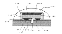
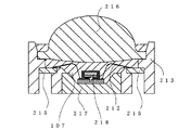
即ち、本願発明にかかる発光装置は、図1に示されるように、支持基板101に実装された発光素子103の側方端面側に形成された第一の波長変換部材104と、発光素子103の主面側を被覆するように形成された第二の波長変換部材105とを有する。第一、第二の波長変換部材104、105は、蛍光体とともに該蛍光体を固着させる結着剤により構成されている。また、第一の波長変換部材104の上端部は、支持基板101の主面からの高さが、発光素子103の主面より高くなるように形成されている。したがって、第一の波長変換部材104の上端部が第二の波長変換部材105の障壁となり、第二の波長変換部材105が発光素子103の主面側からこぼれ落ちないように構成されている。このような構成は、発光観測面をレベリングさせて平滑面とすることを目的として、未硬化の状態で流動性を有する樹脂を結着剤としたとき特に効果がある。さらに、上記波長変換部材は、上記発光素子の側方において、発熱体であるバンプ102から離間されており、熱に弱い蛍光体の輝度の低下を抑制し、発光効率の高い発光装置とすることができる。
That is, as shown in FIG. 1, the light emitting device according to the present invention includes a first
また、発光素子と、該発光素子からの光の少なくとも一部を吸収して異なる波長を有する光を発光する蛍光物質を含有する波長変換部材とを有する発光装置の形成方法において、本願発明者らは、上記発光素子の外周に沿うように蛍光物質と結着剤との混合物を供給する第一の工程と、上記混合物を障壁として位置決めし、上記発光素子の主面側に蛍光物質と結着剤との混合物を供給する第二の工程と、上記混合物のうち少なくとも一方を硬化させる第三の工程とを含む発光装置の形成方法とすることにより上述したような課題を解決するに至った。 Further, in a method for forming a light-emitting device including a light-emitting element and a wavelength conversion member containing a fluorescent material that emits light having a different wavelength by absorbing at least part of light from the light-emitting element, the inventors of the present application. A first step of supplying a mixture of a fluorescent substance and a binder along the outer periphery of the light emitting element, positioning the mixture as a barrier, and binding the fluorescent substance on the main surface side of the light emitting element By forming a light emitting device forming method including a second step of supplying a mixture with an agent and a third step of curing at least one of the mixtures, the above-described problems have been solved.
即ち、本願発明にかかる発光装置の形成方法は、少なくとも以下の工程Aから工程Cを含むことを特徴とする。図9は、本願発明にかかる発光装置の形成方法のうち、工程Aの一実施例を模式的に示す斜視図である。図10、図11および図12は、本願発明にかかる発光装置の形成方法のうち、工程Bの一実施例を模式的に示す斜視図および断面図である。 That is, the method for forming a light emitting device according to the present invention includes at least the following steps A to C. FIG. 9 is a perspective view schematically showing one embodiment of step A in the method for forming a light emitting device according to the present invention. 10, FIG. 11 and FIG. 12 are a perspective view and a cross-sectional view schematically showing an example of the process B in the method for forming a light emitting device according to the present invention.
工程A;図9に示されるように、支持基板に実装された発光素子の外周に沿って、発光素子の側面方向に蛍光物質と結着剤である樹脂材料との混合物(以下、「硬化性組成物」と呼ぶことがある。)を配置させる。このとき、図1あるいは図5に示されるように、発光素子の側面と混合物の外壁面との距離aは、発光素子が実装されている側の支持基板の主面から混合物の上端部までの距離b(第一の波長変換部材の高さ;b)と、上記支持基板の主面から発光素子の発光観測面側主面までの距離hとの差分(b−h)(上端部の厚み)とほぼ等しいことが好ましい。言い換えると、第一の波長変換部材を形成する混合物の上端部は、発光素子の側面と混合物の外壁面との距離aだけ、透光性基板210の発光観測面側主面から突出するように配置することが好ましい。これにより、発光素子は、均一な厚みを有する波長変換部材にて被覆され、発光観測方位によって色温度の変化が少ない発光装置とすることができる。
Step A: As shown in FIG. 9, along the outer periphery of the light-emitting element mounted on the support substrate, a mixture of a fluorescent material and a resin material as a binder (hereinafter referred to as “curability”) in the lateral direction of the light-emitting element. "Sometimes referred to as a" composition "). At this time, as shown in FIG. 1 or FIG. 5, the distance a between the side surface of the light emitting element and the outer wall surface of the mixture is from the main surface of the support substrate on the side where the light emitting element is mounted to the upper end of the mixture. Difference (b−h) (thickness of upper end portion) between distance b (height of first wavelength conversion member; b) and distance h from the main surface of the support substrate to the main surface of the light emitting element on the light emission observation surface side Is preferably substantially equal to). In other words, the upper end portion of the mixture forming the first wavelength conversion member protrudes from the emission observation surface side main surface of the
本工程における形成方法は、図9に示されるディスペンサー202を利用した方法である。なお、本形態ではディペンサーを利用するが、メタルマスク法や、以下の工程で利用されるスクリーン印刷による形成方法により、蛍光体含有の樹脂材料を配置させてもよい。また、本発明による形成方法によれば、異なる種類の蛍光体含有の樹脂材料を発光素子の側方端面側のみに多層に配置させることも容易にできる。
The forming method in this step is a method using the
工程B;図10および図11に示されるように、発光素子の上面を被覆するようにディスペンサーを利用したポッティング、あるいは図12に示されるように、スクリーン印刷にて蛍光体含有の樹脂材料を配置させる。例えば、ディスペンサーを利用するとき、図10に示されるように、工程Aにて配置された硬化性組成物201の縁に沿うように硬化性組成物203を発光素子103主面へ供給した後、発光素子103主面の中心方向に向かって渦巻き状かつ連続的に硬化性組成物203を供給することができる。また、図11に示されるように、工程Aにて配置された硬化性組成物201の方向へ、発光素子103の中心付近から渦巻き状かつ連続的に硬化性組成物203を供給することができる。このとき、硬化性組成物203が供給される途中で、含有される蛍光物質の種類を変更したり、拡散剤を含有させたりすることもできる。これにより、種類の異なる蛍光体相互間における発光の吸収および発光装置の配光特性を考慮し、発光効率の高い発光装置とすることができる。
Step B: Potting using a dispenser to cover the upper surface of the light emitting element as shown in FIGS. 10 and 11, or arranging a phosphor-containing resin material by screen printing as shown in FIG. Let For example, when using a dispenser, as shown in FIG. 10, after supplying the curable composition 203 to the main surface of the
本工程において、工程Aにて配置させた混合物、あるいはそれが硬化された第一の波長変換部材は、本工程において供給される混合物の流動を妨げる障壁となり、供給される硬化性組成物203の位置決めを行うことが容易にできる。即ち、発光素子が実装されている側の支持基板の主面から混合物の上端部までの距離bと、上記支持基板の主面から発光素子の発光観測面側主面までの距離hとの差分(b−h)が障壁の高さとなり、また本工程において供給される硬化性組成物203の厚みcとなる。また、この厚みcは、発光素子の側面と混合物の外壁面との距離aと等しくすることができる。これにより、発光素子は、均一な厚みを有する第一、第二の波長変換部材104、105にて被覆され、発光観測方位によって色温度の変化が少ない発光装置とすることができる。また、上記工程Aにて配置させた混合物より、含有される蛍光体の量を大きくしたり、小さくしたりすることができる。
In this step, the mixture disposed in step A or the first wavelength conversion member on which it is cured serves as a barrier that prevents the flow of the mixture supplied in this step, and the curable composition 203 supplied It is easy to perform positioning. That is, the difference between the distance b from the main surface of the support substrate on the side where the light emitting element is mounted to the upper end of the mixture and the distance h from the main surface of the support substrate to the main surface of the light emitting element on the light emission observation surface side (Bh) is the height of the barrier, and is the thickness c of the curable composition 203 supplied in this step. The thickness c can be made equal to the distance a between the side surface of the light emitting element and the outer wall surface of the mixture. As a result, the light emitting element is covered with the first and second
工程C;所定時間静置させることにより蛍光体含有の混合物の平滑面を得た後、混合物を硬化させることにより、発光素子の側方端部側を被覆するような第一の波長変換部材、および発光素子の主面側を被覆するような第二の波長変換部材を形成する。フリップチップ実装された発光素子と支持基板との間に生じる隙間には、アンダーフィル材として樹脂を供給することが好ましい。このように構成することにより、発光装置の放熱性が向上し、発光素子と支持基板との熱膨張や機械的な応力を緩和させることができるため、発光装置の信頼性を向上させることができる。また、アンダーフィル材が波長変換部材とバンプやサブマウントとを介するように配置されることにより、波長変換部材とバンプやサブマウントを離間させることができる。 Step C: After obtaining a smooth surface of the phosphor-containing mixture by allowing it to stand for a predetermined time, a first wavelength conversion member that covers the side end portion side of the light-emitting element by curing the mixture, And the 2nd wavelength conversion member which coat | covers the main surface side of a light emitting element is formed. It is preferable to supply a resin as an underfill material to a gap generated between the light emitting element mounted on the flip chip and the support substrate. With such a configuration, the heat dissipation of the light emitting device is improved, and the thermal expansion and mechanical stress between the light emitting element and the support substrate can be relieved, so that the reliability of the light emitting device can be improved. . In addition, the wavelength conversion member and the bump or submount can be separated from each other by disposing the underfill material via the wavelength conversion member and the bump or submount.
なお、第一の波長変換部材および第二の波長変換部材を形成する混合物は、別々に硬化させてもよいし、同時に硬化させてもよい。即ち、第一の波長変換部材の材料を硬化させた後、発光素子の主面側に蛍光体含有の樹脂を配置させてもよい。このように別々に硬化させることにより、第二の波長変換部材を形成するための位置決めを容易に行うことができる。また、別々に硬化させることにより、第一の波長変換部材と第二の波長変換部材との界面が生じる。以下、本形態の各構成について詳述する。 In addition, the mixture which forms a 1st wavelength conversion member and a 2nd wavelength conversion member may be hardened separately, and may be hardened simultaneously. That is, after the material of the first wavelength conversion member is cured, a phosphor-containing resin may be disposed on the main surface side of the light emitting element. By separately curing in this way, positioning for forming the second wavelength conversion member can be easily performed. Moreover, the interface of a 1st wavelength conversion member and a 2nd wavelength conversion member arises by making it harden | cure separately. Hereinafter, each structure of this form is explained in full detail.
[波長変換部材]
本形態における波長変換部材は、発光素子の周辺に配置され、発光素子からの光を吸収して異なる波長を含む光を発光可能な部材である。波長変換部材には、有機蛍光体や以下に述べる無機蛍光体のような蛍光物質の他、発光素子からの光を発光観測面方向に散乱させる拡散剤や、発光素子から放出される波長の一部をカットするフィルター効果を持つ着色剤、顔料を含有させることもできる。ここで、第一の波長変換部材および第二の波長変換部材に含有される拡散剤、蛍光物質を固着させる結着剤と蛍光物質との混合比率、種類は同じである必要はない。即ち、第一の波長変換部材と第二の波長変換部材とは、異なる混合比率で、異なる種類の拡散剤や蛍光物質を含有してもよい。また、第一の波長変換部材および第二の波長変換部材は、それぞれ多数隣接させて形成することにより多層構造とすることができる。例えば、図3に示されるように第一の波長変換部材104aおよび104b、第二の波長変換部材105aおよび105bとすることもできる。さらに、このように多層構造としたとき、結着剤、含有される蛍光物質や拡散剤の種類、量および粒径を層ごとに変えたり、屈折率を変化させることができる。以下、発光素子の側方端面側に形成される第一の波長変換部材、発光素子の主面方向に配置される第二の波長変換部材について、それぞれ詳述する。
[Wavelength conversion member]
The wavelength conversion member in the present embodiment is a member that is disposed around the light emitting element and can emit light including different wavelengths by absorbing light from the light emitting element. The wavelength conversion member includes a fluorescent material such as an organic phosphor or an inorganic phosphor described below, a diffusing agent that scatters light from the light emitting element in the direction of the light emission observation surface, and a wavelength emitted from the light emitting element. A colorant or a pigment having a filter effect for cutting off the part can also be contained. Here, the mixing ratio and type of the diffusing agent, the binder for fixing the fluorescent material and the fluorescent material contained in the first wavelength converting member and the second wavelength converting member need not be the same. That is, the first wavelength conversion member and the second wavelength conversion member may contain different types of diffusing agents and fluorescent materials at different mixing ratios. Moreover, the first wavelength conversion member and the second wavelength conversion member can be formed in a multilayer structure by being formed adjacent to each other. For example, as shown in FIG. 3, the first wavelength conversion members 104a and 104b and the second wavelength conversion members 105a and 105b may be used. Further, when the multilayer structure is used as described above, the type, amount and particle size of the binder, the fluorescent material and the diffusing agent contained therein can be changed for each layer, and the refractive index can be changed. Hereinafter, the first wavelength conversion member formed on the side end surface side of the light emitting element and the second wavelength conversion member arranged in the main surface direction of the light emitting element will be described in detail.
(第一の波長変換部材104)
本形態における第一の波長変換部材を形成するための材料としては、タレの生じにくい比較的チキソ性の高い樹脂が結着剤として使用される。このようにチキソ性の高い材料とすることにより、発光素子と支持基板との隙間に入りにくく、導電部材の方にタレないようにすることができる。例えば、封止用樹脂と同一組成(但し、チキソ性が異なる。)のものを使用できる。チキソ性の範囲は、タレや高さ不足を生じない程度に、作業性よく均一高さの形成が容易にできるように調整される。
(First wavelength conversion member 104)
As a material for forming the first wavelength conversion member in the present embodiment, a resin having a relatively high thixotropy that hardly causes sagging is used as a binder. By using a material with high thixotropy in this way, it is difficult to enter the gap between the light emitting element and the support substrate, and the conductive member can be prevented from sagging. For example, a resin having the same composition as the sealing resin (however, the thixotropy is different) can be used. The range of thixotropy is adjusted so that a uniform height can be easily formed with good workability to such an extent that sagging and lack of height do not occur.
第一の波長変換部材の高さは、支持基板に搭載された発光素子の支持基板からの高さとほぼ同程度の高さに形成されるが、これより多少低くても第二の波長変換部材の形成材料を発光素子の主面側に位置決めできる程度の高さがあれば特に問題はない。 The height of the first wavelength conversion member is formed to be substantially the same as the height of the light emitting element mounted on the support substrate from the support substrate, but the second wavelength conversion member may be slightly lower than this. There is no particular problem as long as the forming material is high enough to be positioned on the main surface side of the light emitting element.
第一の波長変換部材を形成するための樹脂材料は、熱硬化性樹脂の場合、加熱硬化時の熱により粘度が低下しないことが好ましい。このような材料としては、封止用樹脂に超微粉のシリカ粉末或いは微細なゴム粒子を樹脂でくるんだコアシェル型の微細粒子を樹脂成分100部に対し、0.1〜10部の範囲で添加したものを挙げることができる。 When the resin material for forming the first wavelength conversion member is a thermosetting resin, it is preferable that the viscosity does not decrease due to heat at the time of heat curing. As such a material, a core-shell type fine particle in which ultrafine silica powder or fine rubber particles are wrapped in a resin for sealing is added in a range of 0.1 to 10 parts per 100 parts of the resin component. Can be mentioned.
発光素子を支持基板に実装させる方法として、発光素子の電極を支持基板の導電パターンに配置したバンプに対向させて、荷重、熱および超音波を加えて接合する方法がある。ここで、本形態において、フリップチップ実装したとき、上述したように、第一の波長変換部材の材料をチキソ性のある材料とすると、その材料は発光素子と支持基板との間に入り込み難く、発光素子と支持基板との間に隙間が生じる。そこで、第一の波長変換部材を形成する材料の配置前に、発光素子と支持基板との間にアンダーフィル材206を注入することが好ましい。図4に示されるように、チキソ性のあるアンダーフィル材206を配置させることにより、第一の波長変換部材104と発熱体であるバンプ102とを離間させて配置することができる。ところで、発光素子103の発熱は、バンプ102を介して支持基板101の方向へ放熱される。したがって、支持基板101は、バンプ102と同様に発熱体となる。本形態において、第一の波長変換部材104は、発熱体である支持基板101からアンダーフィル材206を介し離間させて配置することもできる。このようにアンダーフィル材を発熱体から間隔を空けて配置することにより、第一の波長変換部材に含有される蛍光物質の輝度低下を抑制し、発光効率の高い発光装置とすることができる。
As a method for mounting the light emitting element on the support substrate, there is a method in which the electrode of the light emitting element is opposed to the bump arranged on the conductive pattern of the support substrate and bonded by applying a load, heat and ultrasonic waves. Here, in this embodiment, when flip chip mounting is performed, as described above, if the material of the first wavelength conversion member is a thixotropic material, it is difficult for the material to enter between the light emitting element and the support substrate. A gap is generated between the light emitting element and the support substrate. Therefore, it is preferable to inject an
アンダーフィル材206は、フリップチップ実装前に支持基板に配置されるか、フリップチップ実装後、第一の波長変換部材を形成する材料の配置前に発光素子と支持基板との間に注入され、熱硬化される。アンダーフィルの材料は、例えば、シリコーン樹脂、エポキシ樹脂等の熱硬化性樹脂である。アンダーフィルの熱伝導性を向上させるため、あるいはアンダーフィルの熱応力を緩和させるため、さらに窒化アルミニウム、酸化珪素、酸化アルミニウム及びそれらの複合混合物等が樹脂に混入されてもよい。アンダーフィルの量は、発光素子の正負両電極とサブマウントとの間に生じた隙間を埋めることができる量である。
The
(第二の波長変換部材105)
第一の波長変換部材の形成後、あるいは第一の波長変換部材を形成する材料を配置し硬化前の段階で、発光素子の主面側を被覆するように、外縁が第一の波長変換部材にかかるように第二の波長変換部材の形成材料が配置される。第二の波長変換部材を形成する材料の配置には、孔版印刷、スクリーン印刷およびポッティングのような形成方法が適用される。このような形成方法により配置された第二の波長変換部材の材料は、硬化までの間は流動性を有するが、発光素子の側方端面方向への流動は、先に形成された第一の波長変換部材あるいはその硬化前の材料により阻止される。そのため、第二の波長変換部材の材料は、そのレオロジーと相俟って配置した時点の形状をそのまま保持する。また、第二の波長変換部材の表面は、硬化時までは、その材料が依然流動性を有しているので、自然に平坦になり平滑性が得られる。
(Second wavelength conversion member 105)
After forming the first wavelength conversion member, or before arranging the material for forming the first wavelength conversion member and before curing, the outer edge is the first wavelength conversion member so as to cover the main surface side of the light emitting element. The material for forming the second wavelength conversion member is arranged as described above. Forming methods such as stencil printing, screen printing, and potting are applied to the arrangement of the material forming the second wavelength conversion member. The material of the second wavelength conversion member arranged by such a forming method has fluidity until curing, but the flow in the direction of the side end face of the light emitting element is the first formed first. It is blocked by the wavelength conversion member or the material before curing. Therefore, the material of the second wavelength conversion member retains the shape at the time when the material is disposed in combination with the rheology. Further, since the surface of the second wavelength conversion member is still fluid until it is cured, the surface is naturally flat and smoothness can be obtained.
発光素子を第二の波長変換部材の材料で被覆した後は、その材料を硬化させ、第一の波長変換部材が未硬化の場合は、第一の波長変換部材と共に加熱硬化させる。さらに、本発明の別の実施形態として、各層で蛍光体の種類が異なるように多層構造とされた波長変換部材をストライプ状、同心円状の波長変換部材として発光素子の上面を被覆するように設けることができる。これにより、種類の異なる蛍光体相互間における発光の吸収および発光装置の配光特性を考慮し、発光効率の高い発光装置とすることができる。 After the light emitting element is coated with the material of the second wavelength conversion member, the material is cured, and when the first wavelength conversion member is uncured, the material is heated and cured together with the first wavelength conversion member. Furthermore, as another embodiment of the present invention, a wavelength conversion member having a multilayer structure so that the types of phosphors are different in each layer is provided as a striped or concentric wavelength conversion member so as to cover the upper surface of the light emitting element. be able to. Accordingly, it is possible to obtain a light emitting device with high light emission efficiency in consideration of absorption of light emission between phosphors of different types and light distribution characteristics of the light emitting device.
また、第一の波長変換部材104は、発光観測面側主面を含む平面から突出する上端部を有し、第二の波長変換部材105は、上端部の少なくとも一部を被覆することが好ましい。このように構成することにより、第二の波長変換部材105が発光観測面側主面において固定保持され横方向にズレ動くことがないため、信頼性の高い発光装置とすることができる。
Moreover, it is preferable that the first
また、第二の波長変換部材105は、発光素子の側面と第一の波長変換部材104との間に介在していることが好ましい。このように構成することにより、第二の波長変換部材105が発光素子の発光観測面側主面において強固に固定保持され、脱落することがないため、信頼性の高い発光装置とすることができる。さらに、第一の波長変換部材104と発光素子の側面と第一の波長変換部材104との間に介在している第二の波長変換部材105とで、含有される蛍光体の種類を変えることにより、所望の光学特性を有する発光装置とすることもできる。
The second
上述した第一および第二の波長変換部材を構成する材料であり、蛍光体を固着させる結着剤である材料は、耐光性、透光性に優れた熱硬化性樹脂、例えばエポキシ樹脂、アクリル樹脂、イミド樹脂、シリコン樹脂などの有機物質や、金属アルコキシドを出発原料としてゾルゲル法により得られた透光性無機部材や、ガラスなど無機物質を選択することができる。また、波長変換部材に発光素子からの光を拡散させる目的で酸化アルミニウム、酸化バリウム、チタン酸バリウム、酸化珪素などを含有させることもできる。同様に外来光や発光素子からの不要な波長をカットするフィルター効果を持たすために各種着色剤を添加させることもできる。また、封止樹脂の内部応力を緩和させる各種フィラーを含有させることもできる。 The material constituting the first and second wavelength conversion members described above and the binder for fixing the phosphor is a thermosetting resin excellent in light resistance and translucency, for example, epoxy resin, acrylic An organic substance such as a resin, an imide resin, or a silicon resin, a translucent inorganic member obtained by a sol-gel method using a metal alkoxide as a starting material, or an inorganic substance such as glass can be selected. In addition, aluminum oxide, barium oxide, barium titanate, silicon oxide, or the like can be contained in the wavelength conversion member for the purpose of diffusing light from the light emitting element. Similarly, various colorants can be added in order to have a filter effect of cutting unnecessary wavelengths from extraneous light and light emitting elements. Moreover, various fillers that relieve internal stress of the sealing resin can also be contained.
第一の波長変換部材および第二の波長変換部材は、ともに層厚が20μm〜100μm程度の均一な層とすることができる。また、第一の波長変換部材に含有される蛍光体の量を第二の蛍光体に含有される蛍光体の量より少なくすることができる。これにより、発光観測方位による色温度差が少ない発光装置とすることができる。 Both the first wavelength conversion member and the second wavelength conversion member can be a uniform layer having a layer thickness of about 20 μm to 100 μm. Further, the amount of the phosphor contained in the first wavelength conversion member can be made smaller than the amount of the phosphor contained in the second phosphor. As a result, a light emitting device with a small color temperature difference depending on the light emission observation direction can be obtained.
[蛍光物質106]
本発明では、発光素子の半導体素子構造中、発光素子を被覆する封止部材、発光素子を支持体やリード電極に固着させるダイボンド材、発光素子と支持基板との間に設けられる樹脂層、およびパッケージのような支持基体など、各構成部材中および/または各構成部材の周辺に無機蛍光体や有機蛍光体のような種々の蛍光物質を配置させることができる。また特に、封止部材と組み合わされる蛍光物質は、封止部材の発光観測面側表面を被覆するようにシート状に設けられる他、封止部材の発光観測面側表面あるいは発光素子から離間させた位置に、蛍光体を含む層、蛍光体を含むシートあるいはフィルターとして設けることもできる。このように離間させることにより、発光素子周辺の熱による蛍光体の輝度低下を抑制し、発光効率の高い発光装置とすることができる。
[Fluorescent substance 106]
In the present invention, in the semiconductor element structure of the light emitting element, a sealing member that covers the light emitting element, a die bond material that fixes the light emitting element to a support or a lead electrode, a resin layer provided between the light emitting element and the support substrate, and Various fluorescent materials such as an inorganic phosphor and an organic phosphor can be arranged in and / or around each component such as a support base such as a package. In particular, the fluorescent material combined with the sealing member is provided in a sheet shape so as to cover the light emission observation surface side surface of the sealing member, and is separated from the light emission observation surface side surface of the sealing member or the light emitting element. It can also be provided at a position as a layer containing a phosphor, a sheet containing a phosphor or a filter. By separating them in this manner, it is possible to suppress a decrease in luminance of the phosphor due to heat around the light emitting element and to obtain a light emitting device with high luminous efficiency.
本願発明に利用可能な蛍光体は、発光素子から放出される可視光や紫外光の一部を吸収し、その吸収した光の波長と異なる波長を有する光を発光するものである。特に、本形態に用いられる蛍光体は、少なくとも発光素子から発光された光によって励起され、波長変換した光を発光する蛍光体をいい、該蛍光体を固着させる結着剤とともに波長変換部材を構成する。 The phosphor that can be used in the present invention absorbs part of visible light and ultraviolet light emitted from the light emitting element, and emits light having a wavelength different from the wavelength of the absorbed light. In particular, the phosphor used in this embodiment refers to a phosphor that emits a wavelength-converted light that is excited by at least light emitted from the light-emitting element, and constitutes a wavelength conversion member together with a binder that fixes the phosphor. To do.
発光素子からの光と、蛍光体が発光した光が補色関係などにある場合、それぞれの光を混色させることで白色系の混色光を発光することができる。具体的には、発光素子からの光と、それによって励起され発光する蛍光体の光がそれぞれ光の3原色(赤色系、緑色系、青色系)に相当する場合や発光素子が発光した青色系の光と、それによって励起され発光する蛍光体の黄色系の光が挙げられる。 When the light from the light emitting element and the light emitted from the phosphor are in a complementary color relationship or the like, white mixed color light can be emitted by mixing each light. Specifically, the light emitted from the light emitting element and the phosphor light excited and emitted thereby correspond to the three primary colors of light (red, green, and blue), or the blue light emitted from the light emitting element. And yellow light of a phosphor that is excited to emit light.
発光装置の発光色は、蛍光体と、蛍光体の結着剤として働く各種樹脂やガラス等の無機部材との比率、蛍光体の比重、蛍光体の量および形状などを種々調整すること、及び発光素子の発光波長を選択することにより、混色光の色温度を変化させ電球色領域の光など任意の白色系の色調を提供させることができる。発光装置の外部には、発光素子からの光と蛍光体からの光がモールド部材を効率よく透過することが好ましい。 The emission color of the light-emitting device can be adjusted in various ways such as the ratio between the phosphor and various members such as various resins and glass that act as a binder for the phosphor, the specific gravity of the phosphor, the amount and shape of the phosphor, and By selecting the light emission wavelength of the light emitting element, it is possible to change the color temperature of the mixed color light and provide an arbitrary white color tone such as light in the light bulb color region. It is preferable that the light from the light emitting element and the light from the phosphor efficiently pass through the mold member outside the light emitting device.
このような蛍光体は、気相や液相中で自重によって沈降するため、気相や液相中に分散させ均一に放出させ、特に液相中においては懸濁液を静置させることで、より均一性の高い蛍光体を持つ層を形成させることができる。さらに、所望に応じて複数回繰り返すことにより所望の蛍光体量を形成することができる。 Since such a phosphor settles under its own weight in the gas phase or liquid phase, it is dispersed and uniformly released in the gas phase or liquid phase, and in particular in the liquid phase, the suspension is allowed to stand, A layer having a phosphor with higher uniformity can be formed. Furthermore, a desired phosphor amount can be formed by repeating a plurality of times as desired.
以上のようにして形成される蛍光体は、発光装置の表面上において一層からなる波長変換部材中に二種類以上存在してもよいし、二層からなる波長変換部材中にそれぞれ一種類あるいは二種類以上存在してもよい。このようにすると、異なる種類の蛍光体からの光の混色による白色光が得られる。この場合、各蛍光物質から発光される光をより良く混色しかつ色ムラを減少させるために、各蛍光体の平均粒径及び形状は類似していることが好ましい。 Two or more kinds of phosphors formed as described above may be present in a single-layer wavelength conversion member on the surface of the light-emitting device, or one or two of each of the two-layer wavelength conversion member. There may be more than one type. In this way, white light can be obtained by mixing colors from different types of phosphors. In this case, it is preferable that the average particle diameters and shapes of the phosphors are similar in order to better mix the light emitted from the phosphors and reduce color unevenness.
ここで、本明細書中における蛍光体の中心粒径とは、体積基準粒度分布曲線により得られる値であり、体積基準粒度分布曲線は、レーザ回折・散乱法により蛍光体の粒度分布を測定し得られるものである。具体的には、気温25℃、湿度70%の環境下において、濃度が0.05%であるヘキサメタリン酸ナトリウム水溶液に蛍光体を分散させ、レーザ回折式粒度分布測定装置(SALD−2000A)により、粒径範囲0.03μm〜700μmにて測定し得られたものである。 Here, the central particle diameter of the phosphor in the present specification is a value obtained by a volume-based particle size distribution curve, and the volume-based particle size distribution curve is obtained by measuring the particle size distribution of the phosphor by a laser diffraction / scattering method. It is obtained. Specifically, in an environment where the temperature is 25 ° C. and the humidity is 70%, the phosphor is dispersed in a sodium hexametaphosphate aqueous solution having a concentration of 0.05%, and a laser diffraction particle size distribution analyzer (SALD-2000A) It was obtained by measuring in a particle size range of 0.03 μm to 700 μm.
本実施の形態において使用される蛍光体は、イットリウム・アルミニウム・ガーネット系蛍光体やルテチウム・アルミニウム・ガーネット系蛍光体に代表されるアルミニウム・ガーネット系蛍光体と、赤色系の光を発光可能な蛍光体、特に窒化物系蛍光体とを組み合わせたものを使用することもできる。これらのYAG系蛍光体および窒化物系蛍光体は、混合して波長変換部材中に含有させてもよいし、複数の層から構成される波長変換部材中に別々に含有させてもよい。以下、それぞれの蛍光体について詳細に説明していく。 The phosphors used in the present embodiment are yttrium / aluminum / garnet phosphors and aluminum / garnet phosphors typified by lutetium / aluminum / garnet phosphors and fluorescence capable of emitting red light. In combination, it is also possible to use a combination of a phosphor, particularly a nitride-based phosphor. These YAG phosphors and nitride phosphors may be mixed and contained in the wavelength conversion member, or may be separately contained in the wavelength conversion member composed of a plurality of layers. Hereinafter, each phosphor will be described in detail.
(アルミニウム・ガーネット系蛍光体)
本実施の形態に用いられるアルミニウム・ガーネット系蛍光体とは、Alを含み、かつY、Lu、Sc、La、Gd、Tb、Eu及びSmから選択された少なくとも一つの元素と、Ga及びInから選択された一つの元素とを含み、希土類元素から選択された少なくとも一つの元素で付活された蛍光体であり、LEDチップから発光された可視光や紫外線で励起されて発光する蛍光体である。例えば、Tb2.95Ce0.05Al5O12、Y2.90Ce0.05Tb0.05Al5O12、Y2.94Ce0.05Pr0.01Al5O12、Y2.90Ce0.05Pr0.05Al5O12等が挙げられる。
(Aluminum / garnet phosphor)
The aluminum garnet phosphor used in the present embodiment includes Al and at least one element selected from Y, Lu, Sc, La, Gd, Tb, Eu, and Sm, and Ga and In. It is a phosphor that contains one selected element and is activated by at least one element selected from rare earth elements, and is a phosphor that emits light when excited by visible light or ultraviolet light emitted from an LED chip. . For example, Tb 2.95 Ce 0.05 Al 5 O 12 , Y 2.90 Ce 0.05 Tb 0.05 Al 5 O 12 , Y 2.94 Ce 0.05 Pr 0.01 Al 5 O 12 , Y 2.90 Ce 0.05 Pr 0.05 Al 5 O 12 and the like.
特に本実施の形態において、Yを含み、かつCeあるいはPrで付活され組成の異なる二種類以上のイットリウム・アルミニウム酸化物系蛍光体(イットリウム・アルミニウム・ガーネット系蛍光体(以下、「YAG系蛍光体」と呼ぶ。))が利用される。特に、高輝度且つ長時間の使用時においては(Re1-xSmx)3(Al1-yGay)5O12:Ce(0≦x<1、0≦y≦1、但し、Reは、Y,Gd,Laからなる群より選択される少なくとも一種の元素である。)などが好ましい。 In particular, in the present embodiment, two or more types of yttrium / aluminum oxide phosphors (yttrium / aluminum / garnet phosphors (hereinafter referred to as “YAG phosphors”) containing Y and activated by Ce or Pr and having different compositions. Called "body"))). In particular, at the time of high luminance and long-term use (Re 1-x Sm x) 3 (Al 1-y Ga y) 5 O 12: Ce (0 ≦ x <1,0 ≦ y ≦ 1, where, Re Is at least one element selected from the group consisting of Y, Gd, and La).
(Re1-xSmx)3(Al1-yGay)5O12:Ce蛍光体は、ガーネット構造のため、熱、光及び水分に強く、励起スペクトルのピークが470nm付近などにさせることができる。また、発光ピークも530nm付近にあり720nmまで裾を引くブロードな発光スペクトルを持たせることができる。 (Re 1-x Sm x) 3 (Al 1-y Ga y) 5 O 12: Ce phosphor, for garnet structure, heat, resistant to light and moisture, the peak of the excitation spectrum can be like in the vicinity of 470nm Can do. In addition, the emission peak is in the vicinity of 530 nm, and a broad emission spectrum that extends to 720 nm can be provided.
本発明の発光装置において、蛍光体は、2種類以上の蛍光体を混合させてもよい。即ち、上述したYAG系蛍光体について言えば、Al、Ga、Y、La及びGdやSmの含有量が異なる2種類以上の(Re1-xSmx)3(Al1-yGay)5O12:Ce蛍光体を混合させてRGBの波長成分を増やすことができる。また、現在のところ半導体発光素子の発光波長には、バラツキが生ずるものがあるため2種類以上の蛍光体を混合調整させて所望の白色系の混色光などを得ることができる。具体的には、発光素子の発光波長に合わせて色度点の異なる蛍光体の量を調整し含有させることでその蛍光体間と発光素子で結ばれる色度図上の任意の点を発光させることができる。 In the light emitting device of the present invention, the phosphor may be a mixture of two or more phosphors. That is, speaking the YAG fluorescent material described above, Al, Ga, Y, the content of La and Gd and Sm are two or more kinds of (Re 1-x Sm x) 3 (Al 1-y Ga y) 5 O 12 : Ce phosphors can be mixed to increase RGB wavelength components. At present, there are variations in the emission wavelength of the semiconductor light emitting device, so that two or more kinds of phosphors can be mixed and adjusted to obtain a desired white mixed color light or the like. Specifically, by adjusting the amount of phosphors having different chromaticity points in accordance with the emission wavelength of the light emitting element, the arbitrary points on the chromaticity diagram connected between the phosphors and the light emitting element are caused to emit light. be able to.
発光層に窒化物系化合物半導体を用いた発光素子から発光した青色系の光と、青色光を吸収させるためボディーカラーが黄色である蛍光体から発光する緑色系の光と、赤色系の光とを混色表示させると所望の白色系発光色表示を行うことができる。発光装置はこの混色を起こさせるために蛍光体の粉体やバルクをエポキシ樹脂、アクリル樹脂或いはシリコーン樹脂などの各種樹脂や酸化珪素、酸化アルミニウムなどの透光性無機物中に含有させることもできる。このように蛍光体が含有されたものは、発光素子からの光が透過する程度に薄く形成させたドット状のものや層状ものなど用途に応じて種々用いることができる。蛍光体と透光性無機物との比率や塗布、充填量を種々調整すること及び発光素子の発光波長を選択することにより白色を含め電球色など任意の色調を提供させることができる。 Blue light emitted from a light emitting device using a nitride compound semiconductor in the light emitting layer, green light emitted from a phosphor whose body color is yellow to absorb blue light, red light, When mixed color display is performed, a desired white light emission color display can be performed. In order to cause this color mixture, the light emitting device can contain phosphor powder and bulk in various resins such as epoxy resin, acrylic resin or silicone resin, and translucent inorganic materials such as silicon oxide and aluminum oxide. Such phosphors can be used in various ways depending on the application, such as dot-like and layer-like ones that are formed thin enough to transmit light from the light-emitting element. By adjusting the ratio, coating, and filling amount of the phosphor and the translucent inorganic substance and selecting the emission wavelength of the light emitting element, it is possible to provide an arbitrary color tone such as a light bulb color including white.
また、2種類以上の蛍光体をそれぞれ発光素子からの入射光に対して順に配置させることによって効率よく発光可能な発光装置とすることができる。即ち、反射部材を有する発光素子上には、長波長側に吸収波長があり長波長に発光可能な蛍光体が含有された色変換部材と、それよりも長波長側に吸収波長がありより長波長に発光可能な色変換部材とを積層などさせることで反射光を有効利用することができる。 Further, by arranging two or more kinds of phosphors in order with respect to the incident light from the light emitting element, a light emitting device capable of emitting light efficiently can be obtained. That is, on a light emitting element having a reflective member, a color conversion member containing a phosphor that has an absorption wavelength on the long wavelength side and can emit light at a long wavelength, and an absorption wavelength on the longer wavelength side that has a longer wavelength. The reflected light can be used effectively by laminating a color conversion member capable of emitting light at a wavelength.
YAG系蛍光体を使用すると、放射照度として(Ee)=0.1W・cm−2以上1000W・cm−2以下の発光素子と接する或いは近接して配置された場合においても高効率に十分な耐光性を有する発光装置とすることができる。 When a YAG phosphor is used, sufficient light resistance with high efficiency even when it is placed in contact with or close to a light emitting element having an irradiance of (Ee) = 0.1 W · cm −2 to 1000 W · cm −2 The light emitting device can be made to have the property.
本実施の形態に用いられるセリウムで付活された緑色系が発光可能なYAG系蛍光体では、ガーネット構造のため、熱、光及び水分に強く、励起吸収スペクトルのピーク波長が420nmから470nm付近にさせることができる。また、発光ピーク波長λpも510nm付近にあり700nm付近まで裾を引くブロードな発光スペクトルを持つ。一方、セリウムで付活されたイットリウム・アルミニウム酸化物系蛍光体である赤色系が発光可能なYAG系蛍光体でも、ガーネット構造であり熱、光及び水分に強く、励起吸収スペクトルのピーク波長が420nmから470nm付近にさせることができる。また、発光ピーク波長λpが600nm付近にあり750nm付近まで裾を引くブロードな発光スペクトルを持つ。 The cerium-activated YAG-based phosphor used in this embodiment and capable of emitting green light has a garnet structure and is resistant to heat, light, and moisture, and the peak wavelength of the excitation absorption spectrum is in the vicinity of 420 nm to 470 nm. Can be made. Also, the emission peak wavelength λp is near 510 nm, and has a broad emission spectrum that extends to the vicinity of 700 nm. On the other hand, the YAG phosphor that emits red light, which is an yttrium-aluminum oxide phosphor activated by cerium, has a garnet structure, is resistant to heat, light and moisture, and has a peak wavelength of 420 nm in the excitation absorption spectrum. To about 470 nm. Further, the emission peak wavelength λp is in the vicinity of 600 nm, and has a broad emission spectrum that extends to the vicinity of 750 nm.
ガーネット構造を持ったYAG系蛍光体の組成の内、Alの一部をGaで置換することで発光スペクトルが短波長側にシフトし、また組成のYの一部をGd及び/又はLaで置換することで、発光スペクトルが長波長側へシフトする。このように組成を変化することで発光色を連続的に調節することが可能である。したがって、長波長側の強度がGdの組成比で連続的に変えられるなど窒化物半導体の青色系発光を利用して白色系発光に変換するための理想条件を備えている。Yの置換が2割未満では、緑色成分が大きく赤色成分が少なくなり、8割以上では、赤み成分が増えるものの輝度が急激に低下する。また、励起吸収スペクトルについても同様に、ガーネット構造を持ったYAG系蛍光体の組成の内、Alの一部をGaで置換することで励起吸収スペクトルが短波長側にシフトし、また組成のYの一部をGd及び/又はLaで置換することで、励起吸収スペクトルが長波長側へシフトする。YAG系蛍光体の励起吸収スペクトルのピーク波長は、発光素子の発光スペクトルのピーク波長より短波長側にあることが好ましい。このように構成すると、発光素子に投入する電流を増加させた場合、励起吸収スペクトルのピーク波長は、発光素子の発光スペクトルのピーク波長にほぼ一致するため、蛍光体の励起効率を低下させることなく、色度ズレの発生を抑えた発光装置を形成することができる。 Of the composition of YAG phosphors with a garnet structure, the emission spectrum is shifted to the short wavelength side by substituting part of Al with Ga, and part of Y of the composition is replaced with Gd and / or La. By doing so, the emission spectrum shifts to the long wavelength side. In this way, it is possible to continuously adjust the emission color by changing the composition. Therefore, an ideal condition for converting white light emission by using blue light emission of the nitride semiconductor is provided such that the intensity on the long wavelength side is continuously changed by the composition ratio of Gd. If the substitution of Y is less than 20%, the green component is large and the red component is small, and if it is 80% or more, the redness component is increased but the luminance is drastically decreased. Similarly, the excitation absorption spectrum is shifted to the short wavelength side by substituting part of Al with Ga in the composition of the YAG phosphor having a garnet structure. By substituting a part of Gd and / or La, the excitation absorption spectrum is shifted to the longer wavelength side. The peak wavelength of the excitation absorption spectrum of the YAG phosphor is preferably on the shorter wavelength side than the peak wavelength of the emission spectrum of the light emitting element. With this configuration, when the current input to the light emitting element is increased, the peak wavelength of the excitation absorption spectrum substantially matches the peak wavelength of the emission spectrum of the light emitting element, so that the excitation efficiency of the phosphor is not reduced. Thus, a light emitting device in which the occurrence of chromaticity deviation is suppressed can be formed.
アルミニウム・ガーネット系蛍光体は、以下のような方法で製造することができる。まず、蛍光体は、Y、Gd、Ce、La、Al、Sm、Pr、Tb及びGaの原料として酸化物、又は高温で容易に酸化物になる化合物を使用し、それらを化学量論比で十分に混合して原料を得る。又は、Y、Gd、Ce、La、Sm、Pr、Tbの希土類元素を化学量論比で酸に溶解した溶解液を蓚酸で共沈したものを焼成して得られる共沈酸化物と、酸化アルミニウム、酸化ガリウムとを混合して混合原料を得る。これにフラックスとしてフッ化アンモニウム等のフッ化物を適量混合して坩堝に詰め、空気中1350〜1450°Cの温度範囲で2〜5時間焼成して焼成品を得、次に焼成品を水中でボールミルして、洗浄、分離、乾燥、最後に篩を通すことで得ることができる。また、別の実施の形態の蛍光体の製造方法では、蛍光体の原料を混合した混合原料とフラックスからなる混合物を、大気中又は弱還元雰囲気中にて行う第一焼成工程と、還元雰囲気中にて行う第二焼成工程とからなる、二段階で焼成することが好ましい。ここで、弱還元雰囲気とは、混合原料から所望の蛍光体を形成する反応過程において必要な酸素量は少なくとも含むように設定された弱い還元雰囲気のことをいい、この弱還元雰囲気中において所望とする蛍光体の構造形成が完了するまで第一焼成工程を行うことにより、蛍光体の黒変を防止し、かつ光の吸収効率の低下を防止できる。また、第二焼成工程における還元雰囲気とは、弱還元雰囲気より強い還元雰囲気をいう。このように二段階で焼成すると、励起波長の吸収効率の高い蛍光体が得られる。従って、このように形成された蛍光体にて発光装置を形成した場合に、所望とする色調を得るために必要な蛍光体量を減らすことができ、光取り出し効率の高い発光装置を形成することができる。 The aluminum garnet phosphor can be manufactured by the following method. First, phosphors use oxides or compounds that easily become oxides at high temperatures as raw materials for Y, Gd, Ce, La, Al, Sm, Pr, Tb and Ga, and they are added in a stoichiometric ratio. Mix thoroughly to obtain the raw material. Or a coprecipitated oxide obtained by calcining a solution obtained by coprecipitation of oxalic acid with a solution obtained by dissolving a rare earth element of Y, Gd, Ce, La, Sm, Pr, and Tb in an acid at a stoichiometric ratio with acid; Aluminum and gallium oxide are mixed to obtain a mixed raw material. An appropriate amount of fluoride such as ammonium fluoride is mixed with this as a flux and packed in a crucible, fired in air at a temperature range of 1350 to 1450 ° C. for 2 to 5 hours to obtain a fired product, and then the fired product in water. It can be obtained by ball milling, washing, separating, drying and finally passing through a sieve. Further, in the method for manufacturing a phosphor according to another embodiment, a first firing step in which a mixture composed of a mixture of phosphor materials and a flux is mixed in the atmosphere or in a weak reducing atmosphere, and in a reducing atmosphere. It is preferable to perform the baking in two stages, which includes the second baking step performed in step (b). Here, the weak reducing atmosphere refers to a weak reducing atmosphere set to include at least the amount of oxygen necessary in the reaction process of forming a desired phosphor from the mixed raw material. By performing the first firing step until the formation of the phosphor structure is completed, blackening of the phosphor can be prevented and a decrease in light absorption efficiency can be prevented. In addition, the reducing atmosphere in the second firing step refers to a reducing atmosphere stronger than the weak reducing atmosphere. By firing in two stages in this way, a phosphor with high absorption efficiency at the excitation wavelength can be obtained. Therefore, when a light emitting device is formed with the phosphor thus formed, the amount of the phosphor necessary for obtaining a desired color tone can be reduced, and a light emitting device with high light extraction efficiency can be formed. Can do.
組成の異なる2種類以上のセリウムで付活されたアルミニウム・ガーネット系蛍光体は、混合させて用いても良いし、それぞれ独立して配置させても良い。蛍光体をそれぞれ独立して配置させる場合、発光素子から光をより短波長側で吸収発光しやすい蛍光体、それよりも長波長側で吸収発光しやすい蛍光体の順に配置させることが好ましい。これによって効率よく吸収及び発光させることができる。
(ルテチウム・アルミニウム・ガーネット系蛍光体)
ルテチウム・アルミニウム・ガーネット系蛍光体とは、一般式(Lu1−a−bRaMb)3(Al1−cGac)5O12(但し、RはCeを必須とする少なくとも1種以上の希土類元素である。MはSc、Y、La、Gdから選択される少なくとも1種の元素であり、0.0001≦a≦0.5、0≦b≦0.5、0.0001≦a+b<1、0≦c≦0.8である。)で表される蛍光体である。例えば、組成式が(Lu0.99Ce0.01)3Al5O12、(Lu0.90Ce0.10)3Al5O12、(Lu0.99Ce0.01)3(Al0.5Ga0.5)5O12で表される蛍光体である。
Aluminum and garnet phosphors activated with two or more types of cerium having different compositions may be mixed or used independently. When the phosphors are arranged independently, it is preferable to arrange the phosphors in the order of the phosphor that easily absorbs and emits light from the light emitting element on the shorter wavelength side, and the phosphor that easily absorbs and emits light on the longer wavelength side. This makes it possible to efficiently absorb and emit light.
(Lutetium / Aluminum / Garnet phosphor)
The lutetium / aluminum / garnet phosphor is a general formula (Lu 1-ab R a M b ) 3 (Al 1-c Ga c ) 5 O 12 (provided that R is at least one element in which Ce is essential). The above rare earth elements, M is at least one element selected from Sc, Y, La, and Gd, and 0.0001 ≦ a ≦ 0.5, 0 ≦ b ≦ 0.5, 0.0001 ≦ a + b <1, 0 ≦ c ≦ 0.8.) For example, the composition formula is (Lu 0.99 Ce 0.01 ) 3 Al 5 O 12 , (Lu 0.90 Ce 0.10 ) 3 Al 5 O 12 , (Lu 0.99 Ce 0.01 ) 3 (Al a phosphor represented by 0.5 Ga 0.5) 5 O 12.
ルテチウム・アルミニウム・ガーネット系蛍光体(以下、「LAG系蛍光体」と呼ぶことがある。)は、次のようにして得られる。蛍光体原料として、ルテチウム化合物、希土類元素Rの化合物、希土類元素Mの化合物、アルミニウム化合物及びガリウム化合物を用い、各化合物について上記一般式の割合になるように秤取し、混合するか、又はこれら蛍光体原料にフラックスを加えて混合し、原料混合物を得る。この原料混合物をルツボに充填後、還元性雰囲気中、1200〜1600℃で焼成し、冷却後、分散処理することにより、上記一般式で表される本発明の蛍光体を得る。 The lutetium / aluminum / garnet phosphor (hereinafter sometimes referred to as “LAG phosphor”) is obtained as follows. As a phosphor raw material, a lutetium compound, a rare earth element R compound, a rare earth element M compound, an aluminum compound, and a gallium compound are used, and each compound is weighed and mixed so as to have the ratio of the above general formula, or these are mixed. Flux is added to the phosphor material and mixed to obtain a material mixture. After filling this raw material mixture into a crucible, it is fired at 1200 to 1600 ° C. in a reducing atmosphere, and after cooling, the phosphor of the present invention represented by the above general formula is obtained by dispersion treatment.
蛍光体原料として、酸化物又は熱分解により酸化物となる炭酸塩、水酸化物等の化合物が好ましく用いられる。また、蛍光体原料として、蛍光体を構成する各金属元素を全部又は一部含む共沈物を用いることもできる。例えば、これらの元素を含む水溶液にアルカリ、炭酸塩等の水溶液を加えると共沈物が得られるが、これを乾燥又は熱分解して用いることができる。また、フラックスとしてはフッ化物、ホウ酸塩等が好ましく、蛍光体原料100重量部に対し0.01〜1.0重量部の範囲で添加する。焼成雰囲気は、付活剤のセリウムが酸化されない還元性雰囲気が好ましい。水素濃度が3.0体積%以下の水素・窒素の混合ガス雰囲気がより好ましい。焼成温度は1200〜1600℃が好ましく、目的の中心粒径の蛍光体を得ることができる。より好ましくは1300〜1500℃である。 As the phosphor raw material, an oxide or a compound such as a carbonate or hydroxide that becomes an oxide by thermal decomposition is preferably used. Moreover, the coprecipitate which contains all or one part of each metal element which comprises a fluorescent substance can also be used as a fluorescent substance raw material. For example, when an aqueous solution such as alkali or carbonate is added to an aqueous solution containing these elements, a coprecipitate can be obtained, which can be used after being dried or thermally decomposed. Moreover, as a flux, a fluoride, a borate, etc. are preferable, and it adds in 0.01-1.0 weight part with respect to 100 weight part of fluorescent substance raw materials. The firing atmosphere is preferably a reducing atmosphere in which the activator cerium is not oxidized. A mixed gas atmosphere of hydrogen and nitrogen having a hydrogen concentration of 3.0% by volume or less is more preferable. The firing temperature is preferably 1200 to 1600 ° C., and a phosphor having a target center particle diameter can be obtained. More preferably, it is 1300-1500 degreeC.
上記一般式において、Rは付活剤であり、Ceを必須とする少なくとも1種以上の希土類元素であって、具体的には、Ce、La、Pr、Nd、Sm、Eu、Gd、Tb、Dy、Ho、Er、Tm、Yb、Lrである。RはCeのみでもよいが、CeとCe以外の希土類元素から選ばれる少なくとも1種以上の元素とを含んでいてもよい。Ce以外の希土類元素は、共付活剤として作用するためである。ここで、Rには、CeがR全量に対し70mol%以上含有されていることが好ましい。a値(R量)は、0.0001≦a≦0.5が好ましく、0.0001未満では発光輝度が低下し、0.5を越えても濃度消光によって発光輝度が低下する。より好ましくは、0.001≦a≦0.4、さらに好ましくは、0.005≦a≦0.2である。b値(M量)は、0≦b≦0.5が好ましく、より好ましくは0≦b≦0.4であり、さらに好ましくは0≦b≦0.3である。例えば、MがYの場合、b値が0.5を越えると長波長紫外線〜短波長可視光、特に360〜410nm励起による発光輝度が非常に低下してしまう。c値(Ga量)は、0≦c≦0.8が好ましく、より好ましくは0≦c≦0.5であり、さらに好ましくは0≦c≦0.3である。c値が0.8を越えると発光波長は短波長にシフトし、発光輝度が低下する。 In the above general formula, R is an activator and is at least one or more rare earth elements essential for Ce, specifically, Ce, La, Pr, Nd, Sm, Eu, Gd, Tb, Dy, Ho, Er, Tm, Yb, and Lr. R may be Ce alone, but may contain Ce and at least one element selected from rare earth elements other than Ce. This is because rare earth elements other than Ce act as coactivators. Here, it is preferable that Ce contains 70 mol% or more of Ce with respect to the total amount of R. The a value (R amount) is preferably 0.0001 ≦ a ≦ 0.5. If the value is less than 0.0001, the light emission luminance is lowered, and if it exceeds 0.5, the light emission luminance is lowered by concentration quenching. More preferably, 0.001 ≦ a ≦ 0.4, and still more preferably 0.005 ≦ a ≦ 0.2. The b value (M amount) is preferably 0 ≦ b ≦ 0.5, more preferably 0 ≦ b ≦ 0.4, and still more preferably 0 ≦ b ≦ 0.3. For example, when M is Y and the b value exceeds 0.5, the emission luminance due to excitation of long-wavelength ultraviolet light to short-wavelength visible light, particularly 360 to 410 nm is extremely lowered. The c value (Ga content) is preferably 0 ≦ c ≦ 0.8, more preferably 0 ≦ c ≦ 0.5, and still more preferably 0 ≦ c ≦ 0.3. When the c value exceeds 0.8, the emission wavelength shifts to a short wavelength, and the emission luminance decreases.
LAG系蛍光体の中心粒径は1〜100μmの範囲が好ましく、より好ましくは5〜50μmの範囲であり、さらに好ましくは5〜15μmの範囲である。1μmより小さい蛍光体は、凝集体を形成しやすい傾向にある。これに対し、5〜50μmの粒径範囲の蛍光体は、光の吸収率及び変換効率が高く、波長変換部材も形成しやすい。このように、光学的に優れた特徴を有する粒径の大きな蛍光体を含有させることにより、発光装置の量産性も向上する。また、上記中心粒径値を有する蛍光体が頻度高く含有されていることが好ましく、頻度値は20%〜50%が好ましい。このように粒径のバラツキが小さい蛍光体を用いることにより、より色ムラが抑制され良好な色調を有する発光装置が得られる。 The center particle size of the LAG phosphor is preferably in the range of 1 to 100 μm, more preferably in the range of 5 to 50 μm, and still more preferably in the range of 5 to 15 μm. Phosphors smaller than 1 μm tend to form aggregates. On the other hand, a phosphor having a particle size in the range of 5 to 50 μm has high light absorptivity and conversion efficiency, and easily forms a wavelength conversion member. As described above, the mass productivity of the light-emitting device is improved by including a phosphor having a large particle diameter and having optically excellent characteristics. Moreover, it is preferable that the fluorescent substance which has the said center particle size value is contained frequently, and 20%-50% of frequency values are preferable. By using a phosphor having a small variation in particle size in this way, a light emitting device having a favorable color tone with more suppressed color unevenness can be obtained.
ルテチウム・アルミニウム・ガーネット系蛍光体は300nm〜550nmの波長域の紫外線又は可視光により効率よく励起され発光することから、波長変換部材に含有される蛍光体として有効に利用することができる。さらに、組成式の異なる複数種のLAG系蛍光体、又はLAG系蛍光体を他の蛍光体とともに用いることにより、発光装置の発光色を種々変化させることができる。半導体発光素子からの青色系の発光と、該発光を吸収し黄色系の発光する蛍光体からの発光との混色により、白色系の混色光を発光する従来の発光装置は、発光素子からの光の一部を透過させて利用するため、構造自体を簡略化できると共に出力向上を行いやすいという利点がある。その一方、上記発光装置は、2色の混色による発光であるため、演色性が十分でなく、改良が求められている。そこで、LAG系蛍光体を利用して白色系の混色光を発する発光装置は、従来の発光装置と比較してその演色性を向上させることができる。また、LAG系蛍光体は、YAG系蛍光体と比較して温度特性に優れるため、劣化、色ずれの少ない発光装置を得ることができる。 Since the lutetium / aluminum / garnet phosphor is efficiently excited and emitted by ultraviolet rays or visible light in a wavelength region of 300 nm to 550 nm, it can be effectively used as a phosphor contained in the wavelength conversion member. Furthermore, by using a plurality of types of LAG phosphors having different composition formulas or LAG phosphors together with other phosphors, the emission color of the light emitting device can be variously changed. A conventional light emitting device that emits white light by mixing blue light emitted from a semiconductor light emitting element and light emitted from a phosphor emitting yellow light by absorbing the light emitted from the light emitting element. Since part of the light is used through transmission, there is an advantage that the structure itself can be simplified and the output can be easily improved. On the other hand, since the light emitting device emits light by mixing two colors, the color rendering properties are not sufficient, and improvement is required. Therefore, a light emitting device that emits white color mixed light using a LAG phosphor can improve its color rendering as compared with a conventional light emitting device. In addition, since the LAG phosphor has excellent temperature characteristics as compared with the YAG phosphor, a light emitting device with little deterioration and color shift can be obtained.
(窒化物系蛍光体)
本発明で使用される蛍光体は、Nを含み、かつBe、Mg、Ca、Sr、Ba、及びZnから選択された少なくとも一つの元素と、C、Si、Ge、Sn、Ti、Zr、及びHfから選択された少なくとも一つの元素とを含み、希土類元素から選択された少なくとも一つの元素で付活された窒化物系蛍光体もしようすることができる。また、本実施の形態に用いられる窒化物系蛍光体としては、LEDチップから発光された可視光、紫外線、及びYAG系蛍光体からの発光を吸収することによって励起され発光する蛍光体をいう。例えば、Ca−Ge−N:Eu,Z系、Sr−Ge−N:Eu,Z系、Sr−Ca−Ge−N:Eu,Z系、Ca−Ge−O−N:Eu,Z系、Sr−Ge−O−N:Eu,Z系、Sr−Ca−Ge−O−N:Eu,Z系、Ba−Si−N:Eu,Z系、Sr−Ba−Si−N:Eu,Z系、Ba−Si−O−N:Eu,Z系、Sr−Ba−Si−O−N:Eu,Z系、Ca−Si−C−N:Eu,Z系、Sr−Si−C−N:Eu,Z系、Sr−Ca−Si−C−N:Eu,Z系、Ca−Si−C−O−N:Eu,Z系、Sr−Si−C−O−N:Eu,Z系、Sr−Ca−Si−C−O−N:Eu,Z系、Mg−Si−N:Eu,Z系、Mg−Ca−Sr−Si−N:Eu,Z系、Sr−Mg−Si−N:Eu,Z系、Mg−Si−O−N:Eu,Z系、Mg−Ca−Sr−Si−O−N:Eu,Z系、Sr−Mg−Si−O−N:Eu,Z系、Ca−Zn−Si−C−N:Eu,Z系、Sr−Zn−Si−C−N:Eu,Z系、Sr−Ca−Zn−Si−C−N:Eu,Z系、Ca−Zn−Si−C−O−N:Eu,Z系、Sr−Zn−Si−C−O−N:Eu,Z系、Sr−Ca−Zn−Si−C−O−N:Eu,Z系、Mg−Zn−Si−N:Eu,Z系、Mg−Ca−Zn−Sr−Si−N:Eu,Z系、Sr−Zn−Mg−Si−N:Eu,Z系、Mg−Zn−Si−O−N:Eu,Z系、Mg−Ca−Zn−Sr−Si−O−N:Eu,Z系、Sr−Mg−Zn−Si−O−N:Eu,Z系、Ca−Zn−Si−Sn−C−N:Eu,Z系、Sr−Zn−Si−Sn−C−N:Eu,Z系、Sr−Ca−Zn−Si−Sn−C−N:Eu,Z系、Ca−Zn−Si−Sn−C−O−N:Eu,Z系、Sr−Zn−Si−Sn−C−O−N:Eu,Z系、Sr−Ca−Zn−Si−Sn−C−O−N:Eu,Z系、Mg−Zn−Si−Sn−N:Eu,Z系、Mg−Ca−Zn−Sr−Si−Sn−N:Eu,Z系、Sr−Zn−Mg−Si−Sn−N:Eu,Z系、Mg−Zn−Si−Sn−O−N:Eu,Z系、Mg−Ca−Zn−Sr−Si−Sn−O−N:Eu,Z系、Sr−Mg−Zn−Si−Sn−O−N:Eu,Z系など種々の組み合わせの蛍光体を製造することができる。希土類元素であることを示すZは、Y、La、Ce、Pr、Nd、Gd、Tb、Dy、Ho、Er、Luのうち少なくとも1種以上が含有されていることが好ましいが、Sc、Sm、Tm、Ybが含有されていてもよい。これらの希土類元素は、単体の他、酸化物、イミド、アミド等の状態で原料中に混合する。希土類元素は、主に安定な3価の電子配置を有するが、Yb、Sm等は2価、Ce、Pr、Tb等は4価の電子配置を有する。酸化物の希土類元素を用いた場合、酸素の関与が蛍光体の発光特性に影響を及ぼす。つまり酸素を含有することにより発光輝度の低下を生じる場合もある。その反面、残光を短くするなどの利点もある。但し、Mnを用いると粒径を大きくすることができ、発光輝度の向上を図ることができる。
(Nitride phosphor)
The phosphor used in the present invention contains N and at least one element selected from Be, Mg, Ca, Sr, Ba, and Zn, and C, Si, Ge, Sn, Ti, Zr, and A nitride-based phosphor containing at least one element selected from Hf and activated by at least one element selected from rare earth elements can also be used. The nitride-based phosphor used in the present embodiment refers to a phosphor that emits light when excited by absorbing visible light, ultraviolet light, and light emitted from the YAG-based phosphor emitted from the LED chip. For example, Ca—Ge—N: Eu, Z system, Sr—Ge—N: Eu, Z system, Sr—Ca—Ge—N: Eu, Z system, Ca—Ge—O—N: Eu, Z system, Sr—Ge—O—N: Eu, Z system, Sr—Ca—Ge—ON: Eu, Z system, Ba—Si—N: Eu, Z system, Sr—Ba—Si—N: Eu, Z Type, Ba-Si-ON: Eu, Z type, Sr-Ba-Si-ON: Eu, Z type, Ca-Si-CN: Eu, Z type, Sr-Si-CN : Eu, Z system, Sr-Ca-Si-CN: Eu, Z system, Ca-Si-C-O-N: Eu, Z system, Sr-Si-C-O-N: Eu, Z system Sr—Ca—Si—C—O—N: Eu, Z series, Mg—Si—N: Eu, Z series, Mg—Ca—Sr—Si—N: Eu, Z series, Sr—Mg—Si— N: Eu, Z-based, Mg-Si-O- : Eu, Z series, Mg-Ca-Sr-Si-ON: Eu, Z series, Sr-Mg-Si-ON: Eu, Z series, Ca-Zn-Si-CN: Eu, Z-based, Sr-Zn-Si-CN: Eu, Z-based, Sr-Ca-Zn-Si-CN: Eu, Z-based, Ca-Zn-Si-CN- Eu: Z System, Sr—Zn—Si—C—O—N: Eu, Z system, Sr—Ca—Zn—Si—C—O—N: Eu, Z system, Mg—Zn—Si—N: Eu, Z system Mg-Ca-Zn-Sr-Si-N: Eu, Z system, Sr-Zn-Mg-Si-N: Eu, Z system, Mg-Zn-Si-O-N: Eu, Z system, Mg- Ca-Zn-Sr-Si-ON: Eu, Z system, Sr-Mg-Zn-Si-ON: Eu, Z system, Ca-Zn-Si-Sn-CN: Eu, Z system , Sr-Zn-Si-S -CN: Eu, Z system, Sr-Ca-Zn-Si-Sn-CN: Eu, Z system, Ca-Zn-Si-Sn-C-O-N: Eu, Z system, Sr- Zn—Si—Sn—C—O—N: Eu, Z series, Sr—Ca—Zn—Si—Sn—C—O—N: Eu, Z series, Mg—Zn—Si—Sn—N: Eu, Z-based, Mg-Ca-Zn-Sr-Si-Sn-N: Eu, Z-based, Sr-Zn-Mg-Si-Sn-N: Eu, Z-based, Mg-Zn-Si-Sn-O-N : Eu, Z series, Mg-Ca-Zn-Sr-Si-Sn-ON: Eu, Z series, Sr-Mg-Zn-Si-Sn-ON: Various combinations such as Eu, Z series A phosphor can be manufactured. Z that indicates a rare earth element preferably contains at least one of Y, La, Ce, Pr, Nd, Gd, Tb, Dy, Ho, Er, and Lu, but Sc, Sm , Tm, Yb may be contained. These rare earth elements are mixed in the raw material in the form of oxides, imides, amides, etc. in addition to simple substances. Rare earth elements mainly have a stable trivalent electron configuration, while Yb, Sm, etc. have a divalent configuration, and Ce, Pr, Tb, etc. have a tetravalent electron configuration. When the rare earth element of the oxide is used, the involvement of oxygen affects the light emission characteristics of the phosphor. In other words, the emission luminance may be reduced by containing oxygen. On the other hand, there are also advantages such as shortening the afterglow. However, when Mn is used, the particle size can be increased and the emission luminance can be improved.
例えば、共付活剤としてLaを使用する。酸化ランタン(La2O3)は、白色の結晶で、空気中に放置すると速やかに炭酸塩に代わるため、不活性ガス雰囲気中で保存する。
例えば、共付活剤としてPrを使用する。酸化プラセオジム(Pr6O11)は、通常の希土類酸化物Z2O3と異なり、非化学量論的酸化物で、プラセオジムのシュウ酸塩、水酸化物、炭酸塩などを空気中で焼く800℃に加熱するとPr6O11の組成をもつ黒色の粉体として得られる。Pr6O11はプラセオジム化合物合成の出発物質となり、高純度のものも市販されている。
For example, La is used as a coactivator. Since lanthanum oxide (La 2 O 3 ) is a white crystal and is quickly replaced with carbonate when left in the air, it is stored in an inert gas atmosphere.
For example, Pr is used as a coactivator. Praseodymium oxide (Pr 6 O 11 ) is a non-stoichiometric oxide, unlike ordinary rare earth oxide Z 2 O 3, and burns praseodymium oxalate, hydroxide, carbonate, etc. in the air 800 When heated to 0 ° C., it is obtained as a black powder having a composition of Pr 6 O 11 . Pr 6 O 11 is a starting material for synthesizing a praseodymium compound, and a high-purity one is also commercially available.
特に本発明に係る蛍光体は、Mnが添加されたSr−Ca−Si−N:Eu、Ca−Si−N:Eu、Sr−Si−N:Eu、Sr−Ca−Si−O−N:Eu、Ca−Si−O−N:Eu、Sr−Si−O−N:Eu系シリコンナイトライドである。この蛍光体の基本構成元素は、一般式LXSiYN(2/3X+4/3Y):Eu若しくはLXSiYOZN(2/3X+4/3Y−2/3Z):Eu(Lは、Sr、Ca、SrとCaのいずれか。)で表される。一般式中、X及びYは、X=2、Y=5又は、X=1、Y=7であることが好ましいが、任意のものも使用できる。具体的には、基本構成元素は、Mnが添加された(SrXCa1−X)2Si5N8:Eu、Sr2Si5N8:Eu、Ca2Si5N8:Eu、SrXCa1−XSi7N10:Eu、SrSi7N10:Eu、CaSi7N10:Euで表される蛍光体を使用することが好ましいが、この蛍光体の組成中には、Mg、Sr、Ca、Ba、Zn、B、Al、Cu、Mn、Cr及びNiからなる群より選ばれる少なくとも1種以上が含有されていてもよい。但し、本発明は、この実施の形態及び実施例に限定されない。
Lは、Sr、Ca、SrとCaのいずれかである。SrとCaは、所望により配合比を変えることができる。
蛍光体の組成にSiを用いることにより安価で結晶性の良好な蛍光体を提供することができる。
In particular, the phosphor according to the present invention includes Sr—Ca—Si—N: Eu, Ca—Si—N: Eu, Sr—Si—N: Eu, and Sr—Ca—Si—O—N with Mn added: Eu, Ca-Si-ON: Eu, Sr-Si-ON: Eu-based silicon nitride. The basic constituent elements of this phosphor are represented by the general formula L X Si Y N (2 / 3X + 4 / 3Y) : Eu or L X Si Y O Z N (2 / 3X + 4 / 3Y-2 / 3Z) : Eu (L is Sr, Ca, or any one of Sr and Ca.) In the general formula, X and Y are preferably X = 2, Y = 5, or X = 1, Y = 7, but any can be used. Specifically, the basic constituent elements, Mn is added (Sr X Ca 1-X) 2 Si 5 N 8: Eu,
L is any one of Sr, Ca, Sr and Ca. The mixing ratio of Sr and Ca can be changed as desired.
By using Si for the composition of the phosphor, it is possible to provide an inexpensive phosphor with good crystallinity.
発光中心に希土類元素であるユウロピウムEuを用いる。ユウロピウムは、主に2価と3価のエネルギー準位を持つ。本発明の蛍光体は、母体のアルカリ土類金属系窒化ケイ素に対して、Eu2+を付活剤として用いる。Eu2+は、酸化されやすく、3価のEu2O3の組成で市販されている。しかし、市販のEu2O3では、Oの関与が大きく、良好な蛍光体が得られにくい。そのため、Eu2O3からOを、系外へ除去したものを使用することが好ましい。たとえば、ユウロピウム単体、窒化ユウロピウムを用いることが好ましい。但し、Mnを添加した場合は、その限りではない。 Europium Eu, which is a rare earth element, is used for the emission center. Europium mainly has bivalent and trivalent energy levels. The phosphor of the present invention uses Eu 2+ as an activator with respect to the base alkaline earth metal silicon nitride. Eu 2+ is easily oxidized and is commercially available with a trivalent Eu 2 O 3 composition. However, in commercially available Eu 2 O 3 , O is greatly involved and it is difficult to obtain a good phosphor. Therefore, it is preferable to use a material obtained by removing O from Eu 2 O 3 out of the system. For example, it is preferable to use europium alone or europium nitride. However, this is not the case when Mn is added.
Sr2Si5N8:Eu,Pr、Ba2Si5N8:Eu,Pr、Mg2Si5N8:Eu,Pr、Zn2Si5N8:Eu,Pr、SrSi7N10:Eu,Pr、BaSi7N10:Eu,Ce、MgSi7N10:Eu,Ce、ZnSi7N10:Eu,Ce、Sr2Ge5N8:Eu,Ce、Ba2Ge5N8:Eu,Pr、Mg2Ge5N8:Eu,Pr、Zn2Ge5N8:Eu,Pr、SrGe7N10:Eu,Ce、BaGe7N10:Eu,Pr、MgGe7N10:Eu,Pr、ZnGe7N10:Eu,Ce、Sr1.8Ca0.2Si5N8:Eu,Pr、Ba1.8Ca0.2Si5N8:Eu,Ce、Mg1.8Ca0.2Si5N8:Eu,Pr、Zn1.8Ca0.2Si5N8:Eu,Ce、Sr0.8Ca0.2Si7N10:Eu,La、Ba0.8Ca0.2Si7N10:Eu,La、Mg0.8Ca0.2Si7N10:Eu,Nd、Zn0.8Ca0.2Si7N10:Eu,Nd、Sr0.8Ca0.2Ge7N10:Eu,Tb、Ba0.8Ca0.2Ge7N10:Eu,Tb、Mg0.8Ca0.2Ge7N10:Eu,Pr、Zn0.8Ca0.2Ge7N10:Eu,Pr、Sr0.8Ca0.2Si6GeN10:Eu,Pr、Ba0.8Ca0.2Si6GeN10:Eu,Pr、Mg0.8Ca0.2Si6GeN10:Eu,Y、Zn0.8Ca0.2Si6GeN10:Eu,Y、Sr2Si5N8:Pr、Ba2Si5N8:Pr、Sr2Si5N8:Tb、BaGe7N10:Ceなどが製造できるがこれに限定されない。 Sr 2 Si 5 N 8: Eu , Pr, Ba 2 Si 5 N 8: Eu, Pr, Mg 2 Si 5 N 8: Eu, Pr, Zn 2 Si 5 N 8: Eu, Pr, SrSi 7 N 10: Eu , Pr, BaSi 7 N 10: Eu, Ce, MgSi 7 N 10: Eu, Ce, ZnSi 7 N 10: Eu, Ce, Sr 2 Ge 5 N 8: Eu, Ce, Ba 2 Ge 5 N 8: Eu, Pr, Mg 2 Ge 5 N 8 : Eu, Pr, Zn 2 Ge 5 N 8: Eu, Pr, SrGe 7 N 10: Eu, Ce, BaGe 7 N 10: Eu, Pr, MgGe 7 N 10: Eu, Pr , ZnGe 7 N 10: Eu, Ce, Sr 1.8 Ca 0.2 Si 5 N 8: Eu, Pr, Ba 1.8 Ca 0.2 Si 5 N 8: Eu, Ce, Mg 1.8 Ca 0 .2 Si 5 N 8 : Eu, Pr, Zn 1.8 Ca 0.2 Si 5 N 8 : Eu, Ce, Sr 0.8 Ca 0.2 Si 7 N 10 : Eu, La, Ba 0.8 Ca 0.2 Si 7 N 10: Eu, La, Mg 0.8 Ca 0.2 Si 7 N 10: Eu, Nd, Zn 0.8 Ca 0.2 Si 7 N 10: Eu, Nd, Sr 0.8 Ca 0.2 Ge 7 N 10: Eu, Tb, Ba 0.8 Ca 0.2 Ge 7 N 10: Eu, Tb, Mg 0.8 Ca 0.2 Ge 7 N 10: Eu, Pr, Zn 0.8 Ca 0.2 Ge 7 N 10 : Eu, Pr, Sr 0.8 Ca 0.2 Si 6 GeN 10 : Eu, Pr, Ba 0.8 Ca 0.2 Si 6 GeN 10 : Eu, Pr, Mg 0.8 Ca 0.2 Si 6 GeN 10: Eu, Y , Zn 0.8 Ca 0.2 Si GeN 10: Eu, Y, Sr 2 Si 5 N 8: Pr, Ba 2 Si 5 N 8: Pr, Sr 2 Si 5 N 8: Tb, BaGe 7 N 10: Ce , etc. can be manufactured without limitation.
添加物であるMnは、Eu2+の拡散を促進し、発光輝度、エネルギー効率、量子効率等の発光効率の向上を図る。Mnは、原料中に含有させるか、又は、製造工程中にMn単体若しくはMn化合物を含有させ、原料と共に焼成する。但し、Mnは、焼成後の基本構成元素中に含有されていないか、含有されていても当初含有量と比べて少量しか残存していない。これは、焼成工程において、Mnが飛散したためであると思われる。
蛍光体には、基本構成元素中に、若しくは、基本構成元素とともに、Mg、Ga,In,Li、Na,K、Re、Mo、Fe,Sr、Ca、Ba、Zn、B、Al、Cu、Mn、Cr、O及びNiからなる群より選ばれる少なくとも1種以上を含有する。これらの元素は、粒径を大きくしたり、発光輝度を高めたりする等の作用を有している。また、B、Al、Mg、Cr及びNiは、残光を抑えることができるという作用を有している。
Mn as an additive promotes diffusion of Eu 2+ and improves luminous efficiency such as luminous luminance, energy efficiency, and quantum efficiency. Mn is contained in the raw material, or contains Mn alone or a Mn compound during the manufacturing process, and is fired together with the raw material. However, Mn is not contained in the basic constituent elements after firing, or even if contained, only a small amount remains compared to the initial content. This is probably because Mn was scattered in the firing step.
The phosphor includes Mg, Ga, In, Li, Na, K, Re, Mo, Fe, Sr, Ca, Ba, Zn, B, Al, Cu, in the basic constituent element or together with the basic constituent element. It contains at least one selected from the group consisting of Mn, Cr, O and Ni. These elements have actions such as increasing the particle diameter and increasing the luminance of light emission. Further, B, Al, Mg, Cr and Ni have an effect that afterglow can be suppressed.
このような窒化物系蛍光体は、発光素子によって発光された青色光の一部を吸収して黄から赤色領域の光を発光する。窒化物系蛍光体をYAG系蛍光体と共に上記の構成を有する発光装置に使用して、発光素子により発光された青色光と、窒化物系蛍光体による黄色から赤色光とが混色により暖色系の白色系の混色光を発光する発光装置を提供する。窒化物系蛍光体の他に加える蛍光体には、セリウムで付活されたイットリウム・アルミニウム酸化物蛍光物質が含有されていることが好ましい。イットリウム・アルミニウム酸化物蛍光物質を含有することにより、所望の色度に調節することができるからである。セリウムで付活されたイットリウム・アルミニウム酸化物蛍光物質は、発光素子により発光された青色光の一部を吸収して黄色領域の光を発光する。ここで、発光素子により発光された青色光と、イットリウム・アルミニウム酸化物蛍光物質の黄色光とが混色により青白い白色に発光する。従って、このイットリウム・アルミニウム酸化物蛍光物質と赤色発光する蛍光体とを、透光性を有するコーティング部材中に一緒に混合し、発光素子により発光された青色光とを組み合わせることにより白色系の混色光を発光する発光装置を提供することができる。特に好ましいのは、色度が色度図における黒体放射の軌跡上に位置する白色系の混色光を発光する発光装置である。但し、所望の色温度の発光装置を提供するため、イットリウム・アルミニウム酸化物蛍光物質の蛍光体量と、赤色発光の蛍光体量を適宜変更することもできる。この白色系の混色光を発光する発光装置は、特殊演色評価数R9の改善を図っている。従来の青色発光素子とセリウムで付活されたイットリウム・アルミニウム酸化物蛍光物質との組合せのみの白色系発光装置は、色温度Tcp=4600K付近において特殊演色評価数R9がほぼ0に近く、赤み成分が不足していた。そのため特殊演色評価数R9を高めることが解決課題となっていたが、本発明において赤色発光の蛍光体をイットリウム・アルミニウム酸化物蛍光物質と共に用いることにより、色温度Tcp=4600K付近において特殊演色評価数R9を40付近まで高めることができる。 Such a nitride-based phosphor absorbs part of the blue light emitted by the light emitting element and emits light in the yellow to red region. Using a nitride-based phosphor together with a YAG-based phosphor in the light-emitting device having the above-described configuration, the blue light emitted from the light-emitting element and the yellow to red light by the nitride-based phosphor are mixed to produce a warm color system. Provided is a light-emitting device that emits white mixed-color light. It is preferable that the phosphor added in addition to the nitride-based phosphor contains an yttrium / aluminum oxide phosphor activated with cerium. This is because it can be adjusted to a desired chromaticity by containing the yttrium aluminum oxide fluorescent material. The yttrium / aluminum oxide phosphor activated with cerium absorbs part of the blue light emitted by the light emitting element and emits light in the yellow region. Here, the blue light emitted from the light emitting element and the yellow light of the yttrium / aluminum oxide fluorescent material emit light blue-white by mixing colors. Therefore, the yttrium / aluminum oxide phosphor and the phosphor emitting red light are mixed together in a translucent coating member and combined with the blue light emitted by the light emitting element, thereby mixing white color. A light-emitting device that emits light can be provided. Particularly preferred is a light-emitting device that emits white mixed color light whose chromaticity is located on the locus of black body radiation in the chromaticity diagram. However, in order to provide a light emitting device having a desired color temperature, the amount of phosphor of the yttrium / aluminum oxide phosphor and the amount of phosphor of red light emission can be appropriately changed. This light-emitting device that emits white-based mixed color light improves the special color rendering index R9. A conventional white light emitting device consisting only of a combination of a blue light emitting element and an yttrium aluminum oxide phosphor activated with cerium has a special color rendering index R9 of almost 0 at a color temperature of Tcp = 4600K, and a reddish component. Was lacking. For this reason, increasing the special color rendering index R9 has been a problem to be solved. However, in the present invention, the special color rendering index near the color temperature Tcp = 4600K is obtained by using the phosphor emitting red light together with the yttrium aluminum oxide phosphor. R9 can be increased to around 40.
次に、本発明に係る蛍光体((SrXCa1−X)2Si5N8:Eu)の製造方法を説明するが、本製造方法に限定されない。上記蛍光体には、Mn、Oが含有されている。
Next, the phosphor according to the present invention: is described a method of manufacturing the ((Sr X Ca 1-X ) 2 Si 5
原料のSr、Caを粉砕する。原料のSr、Caは、単体を使用することが好ましいが、イミド化合物、アミド化合物などの化合物を使用することもできる。また原料Sr、Caには、B、Al、Cu、Mg、Mn、MnO、Mn2O3、Al2O3などを含有するものでもよい。原料のSr、Caは、アルゴン雰囲気中、グローブボックス内で粉砕を行う。粉砕により得られたSr、Caは、平均粒径が約0.1μmから15μmであることが好ましいが、この範囲に限定されない。Sr、Caの純度は、2N以上であることが好ましいが、これに限定されない。より混合状態を良くするため、金属Ca、金属Sr、金属Euのうち少なくとも1以上を合金状態としたのち、窒化し、粉砕後、原料として用いることもできる。 Raw materials Sr and Ca are pulverized. The raw materials Sr and Ca are preferably used alone, but compounds such as imide compounds and amide compounds can also be used. The raw materials Sr and Ca may contain B, Al, Cu, Mg, Mn, MnO, Mn 2 O 3 , Al 2 O 3 and the like. The raw materials Sr and Ca are pulverized in a glove box in an argon atmosphere. Sr and Ca obtained by pulverization preferably have an average particle diameter of about 0.1 μm to 15 μm, but are not limited to this range. The purity of Sr and Ca is preferably 2N or higher, but is not limited thereto. In order to improve the mixed state, at least one of the metal Ca, the metal Sr, and the metal Eu can be alloyed, nitrided, pulverized, and used as a raw material.
原料のSiを粉砕する。原料のSiは、単体を使用することが好ましいが、窒化物化合物、イミド化合物、アミド化合物などを使用することもできる。例えば、Si3N4、Si(NH2)2、Mg2Siなどである。原料のSiの純度は、3N以上のものが好ましいが、Al2O3、Mg、金属ホウ化物(Co3B、Ni3B、CrB)、酸化マンガン、H3BO3、B2O3、Cu2O、CuOなどの化合物が含有されていてもよい。Siも、原料のSr、Caと同様に、アルゴン雰囲気中、若しくは、窒素雰囲気中、グローブボックス内で粉砕を行う。Si化合物の平均粒径は、約0.1μmから15μmであることが好ましい。 The raw material Si is pulverized. The raw material Si is preferably a simple substance, but a nitride compound, an imide compound, an amide compound, or the like can also be used. For example, Si 3 N 4 , Si (NH 2 ) 2 , Mg 2 Si, or the like. The purity of the raw material Si is preferably 3N or more, but Al 2 O 3 , Mg, metal borides (Co 3 B, Ni 3 B, CrB), manganese oxide, H 3 BO 3 , B 2 O 3 , Compounds such as Cu 2 O and CuO may be contained. Si is pulverized in a glove box in an argon atmosphere or a nitrogen atmosphere in the same manner as the raw materials Sr and Ca. The average particle size of the Si compound is preferably about 0.1 μm to 15 μm.
次に、原料のSr、Caを、窒素雰囲気中で窒化する。この反応式を、以下の式1および式2にそれぞれ示す。
Next, the raw materials Sr and Ca are nitrided in a nitrogen atmosphere. This reaction formula is shown in the following
3Sr + N2 → Sr3N2 ・・・(式1)
3Ca + N2 → Ca3N2 ・・・(式2)
Sr、Caを、窒素雰囲気中、600〜900℃、約5時間、窒化する。Sr、Caは、混合して窒化しても良いし、それぞれ個々に窒化しても良い。これにより、Sr、Caの窒化物を得ることができる。Sr、Caの窒化物は、高純度のものが好ましいが、市販のものも使用することができる。
3Sr + N 2 → Sr 3 N 2 (Formula 1)
3Ca + N 2 → Ca 3 N 2 (Formula 2)
Sr and Ca are nitrided in a nitrogen atmosphere at 600 to 900 ° C. for about 5 hours. Sr and Ca may be mixed and nitrided, or may be individually nitrided. Thereby, a nitride of Sr and Ca can be obtained. Sr and Ca nitrides are preferably of high purity, but commercially available ones can also be used.
原料のSiを、窒素雰囲気中で窒化する。この反応式を、以下の式3に示す。
The raw material Si is nitrided in a nitrogen atmosphere. This reaction formula is shown in the following
3Si + 2N2 → Si3N4 ・・・(式3)
ケイ素Siも、窒素雰囲気中、800〜1200℃、約5時間、窒化する。これにより、窒化ケイ素を得る。本発明で使用する窒化ケイ素は、高純度のものが好ましいが、市販のものも使用することができる。
3Si + 2N 2 → Si 3 N 4 (Formula 3)
Silicon Si is also nitrided in a nitrogen atmosphere at 800 to 1200 ° C. for about 5 hours. Thereby, silicon nitride is obtained. The silicon nitride used in the present invention is preferably highly pure, but commercially available ones can also be used.
Sr、Ca若しくはSr−Caの窒化物を粉砕する。Sr、Ca、Sr−Caの窒化物を、アルゴン雰囲気中、若しくは、窒素雰囲気中、グローブボックス内で粉砕を行う。
同様に、Siの窒化物を粉砕する。また、同様に、Euの化合物Eu2O3を粉砕する。Euの化合物として、酸化ユウロピウムを使用するが、金属ユウロピウム、窒化ユウロピウムなども使用可能である。このほか、原料のZは、イミド化合物、アミド化合物を用いることもできる。酸化ユウロピウムは、高純度のものが好ましいが、市販のものも使用することができる。粉砕後のアルカリ土類金属の窒化物、窒化ケイ素及び酸化ユウロピウムの平均粒径は、約0.1μmから15μmであることが好ましい。
Sr, Ca or Sr—Ca nitride is pulverized. Sr, Ca, and Sr—Ca nitrides are pulverized in a glove box in an argon atmosphere or a nitrogen atmosphere.
Similarly, Si nitride is pulverized. Similarly, the Eu compound Eu 2 O 3 is pulverized. Europium oxide is used as the Eu compound, but metal europium, europium nitride, and the like can also be used. In addition, as the raw material Z, an imide compound or an amide compound can be used. Europium oxide is preferably highly purified, but commercially available products can also be used. The average particle size of the alkaline earth metal nitride, silicon nitride and europium oxide after pulverization is preferably about 0.1 μm to 15 μm.
上記原料中には、Mg、Sr、Ca、Ba、Zn、B、Al、Cu、Mn、Cr、O及びNiからなる群より選ばれる少なくとも1種以上が含有されていてもよい。また、Mg、Zn、B等の上記元素を以下の混合工程において、配合量を調節して混合することもできる。これらの化合物は、単独で原料中に添加することもできるが、通常、化合物の形態で添加される。この種の化合物には、H3BO3、Cu2O3、MgCl2、MgO・CaO、Al2O3、金属ホウ化物(CrB、Mg3B2、AlB2、MnB)、B2O3、Cu2O、CuOなどがある。 The raw material may contain at least one selected from the group consisting of Mg, Sr, Ca, Ba, Zn, B, Al, Cu, Mn, Cr, O, and Ni. Further, the above elements such as Mg, Zn, and B can be mixed by adjusting the blending amount in the following mixing step. These compounds can be added alone to the raw material, but are usually added in the form of compounds. Such compounds include H 3 BO 3 , Cu 2 O 3 , MgCl 2 , MgO · CaO, Al 2 O 3 , metal borides (CrB, Mg 3 B 2 , AlB 2 , MnB), B 2 O 3 , Cu 2 O, CuO, and the like.
上記粉砕を行った後、Sr、Ca、Sr−Caの窒化物、Siの窒化物、Euの化合物Eu2O3を混合し、Mnを添加する。これらの混合物は、酸化されやすいため、Ar雰囲気中、又は、窒素雰囲気中、グローブボックス内で、混合を行う。 After the pulverization, Sr, Ca, Sr—Ca nitride, Si nitride, and Eu compound Eu 2 O 3 are mixed, and Mn is added. Since these mixtures are easily oxidized, they are mixed in a glove box in an Ar atmosphere or a nitrogen atmosphere.
最後に、Sr、Ca、Sr−Caの窒化物、Siの窒化物、Euの化合物Eu2O3の混合物をアンモニア雰囲気中で、焼成する。焼成により、Mnが添加された(SrXCa1−X)2Si5N8:Euで表される蛍光体を得ることができる。ただし、各原料の配合比率を変更することにより、目的とする蛍光体の組成を変更することができる。 Finally, a mixture of Sr, Ca, Sr—Ca nitride, Si nitride, and Eu compound Eu 2 O 3 is fired in an ammonia atmosphere. A phosphor represented by (Sr X Ca 1-X ) 2 Si 5 N 8 : Eu to which Mn is added can be obtained by firing. However, the composition of the target phosphor can be changed by changing the blending ratio of each raw material.
焼成は、管状炉、小型炉、高周波炉、メタル炉などを使用することができる。焼成温度は、1200から1700℃の範囲で焼成を行うことができるが、1400から1700℃の焼成温度が好ましい。焼成は、徐々に昇温を行い1200から1500℃で数時間焼成を行う一段階焼成を使用することが好ましいが、800から1000℃で一段階目の焼成を行い、徐々に加熱して1200から1500℃で二段階目の焼成を行う二段階焼成(多段階焼成)を使用することもできる。蛍光体の原料は、窒化ホウ素(BN)材質のるつぼ、ボートを用いて焼成を行うことが好ましい。窒化ホウ素材質のるつぼの他に、アルミナ(Al2O3)材質のるつぼを使用することもできる。 For firing, a tubular furnace, a small furnace, a high-frequency furnace, a metal furnace, or the like can be used. Firing can be performed in the range of 1200 to 1700 ° C., but a firing temperature of 1400 to 1700 ° C. is preferable. It is preferable to use a one-step baking in which the temperature is gradually raised and baking is performed at 1200 to 1500 ° C. for several hours, but the first step baking is performed at 800 to 1000 ° C. Two-stage baking (multi-stage baking) in which the second baking is performed at 1500 ° C. can also be used. The phosphor material is preferably fired using a boron nitride (BN) crucible or boat. Besides the crucible made of boron nitride, a crucible made of alumina (Al 2 O 3 ) can also be used.
以上の製造方法を使用することにより、目的とする蛍光体を得ることが可能である。 By using the above manufacturing method, it is possible to obtain a target phosphor.
本発明の実施例において、赤味を帯びた光を発光する蛍光体として、特に窒化物系蛍光体を使用するが、本発明においては、上述したYAG系蛍光体と赤色系の光を発光可能な蛍光体とを備える発光装置とすることも可能である。このような赤色系の光を発光可能な蛍光体は、波長が400〜600nmの光によって励起されて発光する蛍光体であり、例えば、Y2O2S:Eu、La2O2S:Eu、CaS:Eu、SrS:Eu、ZnS:Mn、ZnCdS:Ag,Al、ZnCdS:Cu,Al等が挙げられる。このようにYAG系蛍光体とともに赤色系の光を発光可能な蛍光体を使用することにより発光装置の演色性を向上させることが可能である。 In the embodiment of the present invention, a nitride-based phosphor is used as the phosphor that emits reddish light. In the present invention, the above-described YAG-based phosphor can emit red light. It is also possible to provide a light emitting device including a simple phosphor. Such a phosphor capable of emitting red light is a phosphor that emits light when excited by light having a wavelength of 400 to 600 nm. For example, Y 2 O 2 S: Eu, La 2 O 2 S: Eu. CaS: Eu, SrS: Eu, ZnS: Mn, ZnCdS: Ag, Al, ZnCdS: Cu, Al and the like. As described above, the color rendering property of the light emitting device can be improved by using the phosphor capable of emitting red light together with the YAG phosphor.
以上のようにして形成されるアルミニウムガーネット系蛍光体、および窒化物系蛍光体に代表される赤色系の光を発光可能な蛍光体は、発光素子の周辺において一層からなる波長変換部材中に二種類以上存在してもよいし、二層からなる波長変換部材中にそれぞれ一種類あるいは二種類以上存在してもよい。このような構成にすると、異なる種類の蛍光体からの光の混色による混色光が得られる。この場合、各蛍光物質から発光される光をより良く混色しかつ色ムラを減少させるために、各蛍光体の平均粒径及び形状は類似していることが好ましい。また、窒化物系蛍光体は、YAG系蛍光体により波長変換された光の一部を吸収してしまうことを考慮して、窒化系蛍光体がYAG系蛍光体より発光素子に近い位置に配置されるように波長変換部材を形成することが好ましい。このように構成することによって、YAG系蛍光体により波長変換された光の一部が窒化物系蛍光体に吸収されてしまうことがなくなり、YAG系蛍光体と窒化物系蛍光体とを混合して含有させた場合と比較して、混色光の演色性を向上させることができる。 The phosphors capable of emitting red light typified by the aluminum garnet-based phosphor and nitride-based phosphor formed as described above are included in two wavelength conversion members in the vicinity of the light-emitting element. One or more types may be present, or one type or two or more types may be present in the two-layer wavelength conversion member. With such a configuration, it is possible to obtain mixed color light by mixing light from different types of phosphors. In this case, it is preferable that the average particle diameters and shapes of the phosphors are similar in order to better mix the light emitted from the phosphors and reduce color unevenness. Also, considering that the nitride-based phosphor absorbs part of the light that has been wavelength-converted by the YAG-based phosphor, the nitride-based phosphor is disposed closer to the light emitting element than the YAG-based phosphor. It is preferable to form the wavelength conversion member as described above. With this configuration, a part of the light wavelength-converted by the YAG phosphor is not absorbed by the nitride phosphor, and the YAG phosphor and the nitride phosphor are mixed. The color rendering properties of mixed color light can be improved as compared with the case where it is contained.
(アルカリ土類金属珪酸塩)
本実施の形態における発光装置は、発光素子が発光した光の一部を吸収し、その吸収した光の波長と異なる波長を有する光を発光する蛍光体として、ユウロピウムで付活されたアルカリ土類金属珪酸塩を有することもできる。アルカリ土類金属珪酸塩は、青色領域の光を励起光とし、暖色系の混色光を発光する発光装置とすることができる。該アルカリ土類金属珪酸塩は、以下のような一般式で表されるアルカリ土類金属オルト珪酸塩が好ましい。
(2−x−y)SrO・x(Ba,Ca)O・(1−a−b−c−d)SiO2・aP2O5bAl2O3cB2O3dGeO2:yEu2+(式中、0<x<1.6、0.005<y<0.5、0<a、b、c、d<0.5である。)
(2−x−y)BaO・x(Sr,Ca)O・(1−a−b−c−d)SiO2・aP2O5bAl2O3cB2O3dGeO2:yEu2+(式中、0.01<x<1.6、0.005<y<0.5、0<a、b、c、d<0.5である。)
ここで、好ましくは、a、b、cおよびdの値のうち、少なくとも一つが0.01より大きい。
(Alkaline earth metal silicate)
The light-emitting device in this embodiment mode uses alkaline earth activated by europium as a phosphor that absorbs part of light emitted from a light-emitting element and emits light having a wavelength different from the wavelength of the absorbed light. It can also have a metal silicate. The alkaline earth metal silicate can be a light-emitting device that emits warm color mixed light using blue light as excitation light. The alkaline earth metal silicate is preferably an alkaline earth metal orthosilicate represented by the following general formula.
(2-x-y) SrO · x (Ba, Ca) O · (1-a-b-c-d)
(2-x-y) BaO · x (Sr, Ca) O · (1-a-b-c-d)
Here, preferably, at least one of the values of a, b, c and d is greater than 0.01.
本実施の形態における発光装置は、アルカリ土類金属塩からなる蛍光体として、上述したアルカリ土類金属珪酸塩の他、ユウロピウムおよび/またはマンガンで付活されたアルカリ土類金属アルミン酸塩やY(V,P,Si)O4:Eu、または次式で示されるアルカリ土類金属−マグネシウム−二珪酸塩を有することもできる。 The light-emitting device in the present embodiment is a phosphor composed of an alkaline earth metal salt. In addition to the alkaline earth metal silicate described above, alkaline earth metal aluminate or Y activated by europium and / or manganese is used. (V, P, Si) O 4 : Eu, or an alkaline earth metal-magnesium-disilicate represented by the following formula:
Me(3−x−y)MgSi2O3:xEu,yMn(式中、0.005<x<0.5、0.005<y<0.5、Meは、Baおよび/またはSrおよび/またはCaを示す。)
次に、本実施の形態におけるアルカリ土類金属珪酸塩からなる蛍光体の製造工程を説明する。
Me (3-xy) MgSi 2 O 3 : xEu, yMn (wherein 0.005 <x <0.5, 0.005 <y <0.5, Me represents Ba and / or Sr and / or Or Ca.)
Next, the manufacturing process of the phosphor made of alkaline earth metal silicate in the present embodiment will be described.
アルカリ土類金属珪酸塩の製造のために、選択した組成に応じて出発物質アルカリ土類金属炭酸塩、二酸化珪素ならびに酸化ユウロピウムの化学量論的量を密に混合し、かつ、蛍光体の製造に常用の固体反応で、還元性雰囲気のもと、温度1100℃および1400℃で所望の蛍光体に変換する。この際、0.2モル未満の塩化アンモニウムまたは他のハロゲン化物を添加することが好ましい。また、必要に応じて珪素の一部をゲルマニウム、ホウ素、アルミニウム、リンで置換することもできるし、ユウロピウムの一部をマンガンで置換することもできる。 For the production of alkaline earth metal silicates, the stoichiometric amounts of the starting materials alkaline earth metal carbonate, silicon dioxide and europium oxide are intimately mixed according to the selected composition, and the phosphor is produced. In a conventional solid reaction, the desired phosphor is converted at a temperature of 1100 ° C. and 1400 ° C. under a reducing atmosphere. At this time, it is preferable to add less than 0.2 mol of ammonium chloride or other halide. If necessary, part of silicon can be replaced with germanium, boron, aluminum, and phosphorus, and part of europium can be replaced with manganese.
上述したような蛍光体、即ち、ユウロピウムおよび/またはマンガンで付活されたアルカリ土類金属アルミン酸塩やY(V,P,Si)O4:Eu、Y2O2S:Eu3+の一つまたはこれらの蛍光体を組み合わせることによって、以下の表に実施例として示されるように、所望の色温度を有する発光色および高い色再現性を得ることができる。 One of the phosphors as described above, ie, alkaline earth metal aluminates activated with europium and / or manganese, Y (V, P, Si) O 4 : Eu, Y 2 O 2 S: Eu 3+ By combining one or these phosphors, as shown in the following table as an example, it is possible to obtain an emission color having a desired color temperature and high color reproducibility.
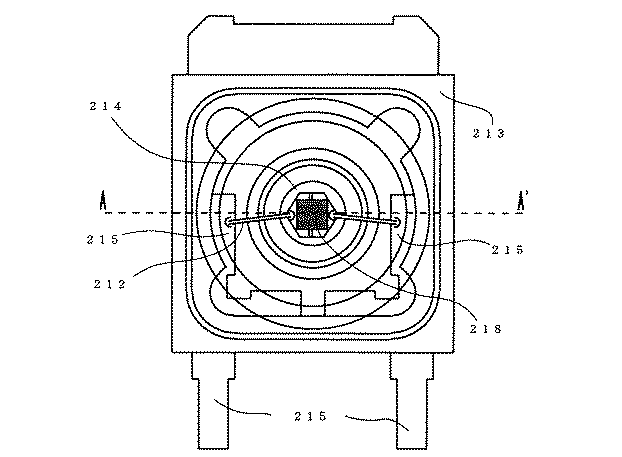
本実施の形態において、蛍光体として紫外光により励起されて発光する蛍光体も用いることができ、具体例として、以下の蛍光体が挙げられる。
(1)Eu、MnまたはEuとMnで付活されたアルカリ土類ハロゲンアパタイト蛍光体;例えば、M5(PO4)3(Cl、Br):Eu(但し、MはSr、Ca、Ba、Mgから選択される少なくとも一種)、Ca10(PO4)6ClBr:Mn、Euなどの蛍光体。
(2)Eu、MnまたはEuとMnで付活されたアルカリ土類アルミン酸塩蛍光体;例えば、BaMg2Al16O27:Eu、BaMg2Al16O27:Eu,Mn、Sr4Al14O25:Eu、SrAl2O4:Eu、CaAl2O4:Eu、BaMgAl10O17:Eu、BaMgAl10O17:Eu,Mnなどの蛍光体。
(3)Euで付活された希土類酸硫化物蛍光体;例えば、La2O2S:Eu、Y2O2S:Eu、Gd2O2S:Euなどの蛍光体。
(4)(Zn、Cd)S:Cu、Zn2GeO4:Mn、3.5MgO・0.5MgF2・GeO2:Mn、Mg6As2O11:Mn、(Mg、Ca、Sr、Ba)Ga2S4:Eu、Ca10(PO4)6FCl:Sb,Mn、や(5)Euで付活された有機錯体蛍光体。
In the present embodiment, a phosphor that emits light when excited by ultraviolet light can also be used as the phosphor, and specific examples include the following phosphors.
(1) Eu, Mn or alkaline earth halogen apatite phosphor activated with Eu and Mn; for example, M 5 (PO 4 ) 3 (Cl, Br): Eu (where M is Sr, Ca, Ba, Phosphors such as at least one selected from Mg), Ca 10 (PO 4 ) 6 ClBr: Mn, Eu.
(2) Eu, Mn or alkaline earth aluminate phosphor activated by Eu and Mn; for example, BaMg 2 Al 16 O 27 : Eu, BaMg 2 Al 16 O 27 : Eu, Mn, Sr 4 Al 14 Phosphors such as O 25 : Eu, SrAl 2 O 4 : Eu, CaAl 2 O 4 : Eu, BaMgAl 10 O 17 : Eu, BaMgAl 10 O 17 : Eu, Mn and the like.
(3) A rare earth oxysulfide phosphor activated with Eu; for example, a phosphor such as La 2 O 2 S: Eu, Y 2 O 2 S: Eu, or Gd 2 O 2 S: Eu.
(4) (Zn, Cd) S: Cu, Zn 2 GeO 4 : Mn, 3.5 MgO · 0.5 MgF 2 · GeO 2 : Mn, Mg 6 As 2 O 11 : Mn, (Mg, Ca, Sr, Ba ) Ga 2 S 4: Eu, Ca 10 (PO 4) 6 FCl: Sb, Mn, and (5) activated organic complex phosphors with Eu.
また、これらの蛍光体は、一層からなる波長変換部材中に単独で用いても良いし、混合して用いてもよい。さらに、二層以上が積層されてなる波長変換部材中にそれぞれ単独で用いても良いし、混合して用いてもよい。 In addition, these phosphors may be used alone in a single-layer wavelength conversion member, or may be used as a mixture. Furthermore, they may be used alone or in combination in a wavelength conversion member in which two or more layers are laminated.
[LEDチップ103]
本形態における発光素子として、LEDチップについて説明する。LEDチップを構成する半導体発光素子としては、ZnSeやGaNなど種々の半導体を使用したものを挙げることができるが、蛍光物質を使用する場合には、その蛍光物質を効率良く励起できる短波長が発光可能な窒化物半導体(InXAlYGa1−X−YN、0≦X、0≦Y、X+Y≦1)が好適に挙げられる。半導体の構造としては、MIS接合、PIN接合やpn接合などを有するホモ構造、ヘテロ構造あるいはダブルへテロ構成のものが挙げられる。半導体層の材料やその混晶度によって発光波長を種々選択することができる。また、半導体活性層を量子効果が生ずる薄膜に形成させた単一量子井戸構造や多重量子井戸構造とすることもできる。
[LED chip 103]
An LED chip will be described as a light emitting element in this embodiment. Examples of semiconductor light-emitting elements that constitute LED chips include those using various semiconductors such as ZnSe and GaN. When a fluorescent material is used, a short wavelength that can excite the fluorescent material efficiently is emitted. possible nitride semiconductor (in X Al Y Ga 1- X-Y N, 0 ≦ X, 0 ≦ Y, X + Y ≦ 1) is preferably exemplified. Examples of the semiconductor structure include a homostructure having a MIS junction, a PIN junction, and a pn junction, a heterostructure, or a double heterostructure. Various emission wavelengths can be selected depending on the material of the semiconductor layer and the degree of mixed crystal. In addition, a single quantum well structure or a multiple quantum well structure in which the semiconductor active layer is formed in a thin film in which a quantum effect is generated can be used.
窒化物半導体を使用した場合、半導体用基板にはサファイヤ、スピネル、SiC、Si、ZnO等の材料が好適に用いられる。結晶性の良い窒化物半導体を量産性よく形成させるためにはサファイヤ基板を用いることが好ましい。このサファイヤ基板上にMOCVD法などを用いて窒化物半導体を形成させることができる。サファイア基板上にGaN、AlN、GaAlN等のバッファー層を形成し、その上にpn接合を有する窒化物半導体を形成させる。 When a nitride semiconductor is used, a material such as sapphire, spinel, SiC, Si, ZnO is preferably used for the semiconductor substrate. In order to form a nitride semiconductor with good crystallinity with high productivity, it is preferable to use a sapphire substrate. A nitride semiconductor can be formed on the sapphire substrate by MOCVD or the like. A buffer layer of GaN, AlN, GaAlN or the like is formed on the sapphire substrate, and a nitride semiconductor having a pn junction is formed thereon.
窒化物半導体を使用したpn接合を有する発光素子の例として、バッファ層上に、n型窒化ガリウムで形成した第1のコンタクト層、n型窒化アルミニウム・ガリウムで形成させた第1のクラッド層、窒化インジウム・ガリウムで形成した活性層、p型窒化アルミニウム・ガリウムで形成した第2のクラッド層、p型窒化ガリウムで形成した第2のコンタクト層を順に積層させたダブルへテロ構成などが挙げられる。 As an example of a light emitting device having a pn junction using a nitride semiconductor, a first contact layer formed of n-type gallium nitride, a first clad layer formed of n-type aluminum nitride / gallium on a buffer layer, Examples include a double hetero structure in which an active layer formed of indium / gallium nitride, a second cladding layer formed of p-type aluminum nitride / gallium, and a second contact layer formed of p-type gallium nitride are sequentially stacked. .
窒化物半導体は、不純物をドープしない状態でn型導電性を示す。発光効率を向上させるなど所望のn型窒化物半導体を形成させる場合は、n型ドーパントとしてSi、Ge、Se、Te、C等を適宜導入することが好ましい。一方、p型窒化物半導体を形成させる場合は、p型ドーパントであるZn、Mg、Be、Ca、Sr、Ba等をドープさせる。窒化物半導体は、p型ドーパントをドープしただけではp型化しにくいためp型ドーパント導入後に、炉による加熱やプラズマ照射等により低抵抗化させることが好ましい。 Nitride semiconductors exhibit n-type conductivity without being doped with impurities. When forming a desired n-type nitride semiconductor, for example, to improve luminous efficiency, it is preferable to appropriately introduce Si, Ge, Se, Te, C, etc. as an n-type dopant. On the other hand, when forming a p-type nitride semiconductor, the p-type dopants such as Zn, Mg, Be, Ca, Sr, and Ba are doped. Since nitride semiconductors are not easily converted to p-type by simply doping with a p-type dopant, it is preferable to reduce resistance by heating in a furnace or plasma irradiation after introducing the p-type dopant.
p型半導体層には、発光素子に投入された電流をp型半導体層の全面に広げるための拡散電極が設けられる。さらに、拡散電極およびn型半導体層には、バンプや導電性ワイヤのような導電部材と接続するp側台座電極およびn側台座電極がそれぞれ設けられる。拡散電極あるいはp側台座電極、およびn側台座電極は、エッチング等の方法によりn型半導体層を露出させた後、蒸着法やスパッタリング法により行う。ここで、互いに平行な正負両電極を形成すると、支持基板に対して安定に実装でき、また、電極間を流れる電流が均一になることにより発光素子の発光面からの発光が均一になるため好ましい。 The p-type semiconductor layer is provided with a diffusion electrode for spreading the current input to the light emitting element over the entire surface of the p-type semiconductor layer. Furthermore, a p-side pedestal electrode and an n-side pedestal electrode connected to a conductive member such as a bump or a conductive wire are provided on the diffusion electrode and the n-type semiconductor layer, respectively. The diffusion electrode, the p-side pedestal electrode, and the n-side pedestal electrode are formed by vapor deposition or sputtering after exposing the n-type semiconductor layer by a method such as etching. Here, it is preferable to form both positive and negative electrodes parallel to each other, because it can be stably mounted on the support substrate, and since the current flowing between the electrodes becomes uniform, the light emission from the light emitting surface of the light emitting element becomes uniform. .
本形態における発光素子は、p側台座電極およびn側台座電極がストライプ状に交互に配列されていることが好ましい。また、p型半導体層に直線状に設けられるp側台座電極の本数は、n側台座電極の本数より多いことが好ましい。また、発光観測面方向から見たときのp側台座電極の幅は、n側台座電極の幅より広い。また、発光観測面方向から見たときのp側台座電極の面積は、n側台座電極の面積より広い。一般に、発光素子は、p型半導体層から下層の半導体積層構造における発熱を如何に放熱させるかが素子の放熱性を向上させる上で問題となる。従って、p側台座電極およびn側台座電極を上述したような構成とし、p側台座電極に設けられる導電部材をn側台座電極より多くすることにより、発光素子の放熱性を向上させることができる。さらに、発光素子の発光に寄与しないn側台座電極が形成されている領域を減らし、p側台座電極の領域を相対的に増やすことで発光素子の光取り出し効率を向上させることができる。本形態においてp側台座電極およびn側台座電極を交互にストライプ状に配列させるとき、n型台座電極のバンプ接合位置は、短冊状のn型台座電極の両隅とする。 In the light-emitting element in this embodiment, it is preferable that p-side pedestal electrodes and n-side pedestal electrodes are alternately arranged in a stripe shape. Moreover, it is preferable that the number of p-side pedestal electrodes provided linearly on the p-type semiconductor layer is larger than the number of n-side pedestal electrodes. Further, the width of the p-side pedestal electrode when viewed from the direction of the emission observation surface is wider than the width of the n-side pedestal electrode. Further, the area of the p-side pedestal electrode when viewed from the light emission observation plane direction is wider than the area of the n-side pedestal electrode. In general, in the light emitting element, how to dissipate heat generated in the semiconductor stacked structure from the p-type semiconductor layer to the lower layer becomes a problem in improving the heat dissipation of the element. Accordingly, the p-side pedestal electrode and the n-side pedestal electrode are configured as described above, and the number of conductive members provided on the p-side pedestal electrode is larger than that of the n-side pedestal electrode, thereby improving the heat dissipation of the light emitting element. . Furthermore, the light extraction efficiency of the light-emitting element can be improved by reducing the area where the n-side pedestal electrode that does not contribute to light emission of the light-emitting element is formed and relatively increasing the area of the p-side pedestal electrode. In this embodiment, when the p-side pedestal electrode and the n-side pedestal electrode are alternately arranged in a stripe shape, the bump bonding position of the n-type pedestal electrode is set to both corners of the strip-shaped n-type pedestal electrode.
本形態において、p側台座電極の材料および/またはp型半導体層側全面に形成される電極は、発光素子の出光を発光素子の透光性基板方向へ反射させる材料とすることが好ましい。例えば、Ag、Al、Rh、Rh/Irが挙げられる。その他、p型半導体層の全面にITO(インジウム(In)とスズ(Sn)の複合酸化物)や、Ni/Au等の金属薄膜を透光性電極として形成させることができる。 In this embodiment, the material of the p-side pedestal electrode and / or the electrode formed on the entire surface of the p-type semiconductor layer is preferably a material that reflects light emitted from the light-emitting element toward the light-transmitting substrate of the light-emitting element. For example, Ag, Al, Rh, Rh / Ir can be mentioned. In addition, a metal thin film such as ITO (complex oxide of indium (In) and tin (Sn)) or Ni / Au can be formed as a translucent electrode on the entire surface of the p-type semiconductor layer.
基板にサファイア等の透光性基板を用いた場合、正負両電極形成後、半導体ウエハーからチップ状にカットすることで、同一面側に正負両電極が設けられた窒化物半導体チップが得られ、発光素子を形成することができる。 When a transparent substrate such as sapphire is used as the substrate, after forming both positive and negative electrodes, by cutting into a chip shape from the semiconductor wafer, a nitride semiconductor chip provided with both positive and negative electrodes on the same surface side is obtained, A light emitting element can be formed.
本発明の発光装置において発光させる場合、蛍光体との補色等を考慮してLEDチップ103の主発光波長は350nm以上530nm以下が好ましい。
When light is emitted in the light emitting device of the present invention, the main light emission wavelength of the
[支持基板101]
本形態における支持基板(サブマウント)は、少なくとも発光素子に対向する面に導電パターンが施される。また、支持基板をリード電極に載置し導通させる構成とする場合には、発光素子に対向する面からリード電極に対向する面にかけて導電部材により導電パターンが施される。本発明における導電パターンは、外部のリード電極から発光素子に電力を供給し、支持基板に対して正負一対の配線パターンが絶縁分離されて形成される。導電パターンの材料とする金属は、金属相互間の接着性の良さ、いわゆる濡れ性等を考慮して選択される。例えば、Auバンプを介して、Auを含むLEDチップの電極とを超音波ダイボンドにより接合するとき、導電パターンは、AuまたはAuを含む合金とする。
[Support substrate 101]
The support substrate (submount) in this embodiment is provided with a conductive pattern on at least a surface facing the light emitting element. In the case where the support substrate is placed on the lead electrode to conduct, the conductive pattern is applied by the conductive member from the surface facing the light emitting element to the surface facing the lead electrode. The conductive pattern in the present invention is formed by supplying electric power from the external lead electrode to the light emitting element, and a pair of positive and negative wiring patterns are insulated and separated from the support substrate. The metal used as the material of the conductive pattern is selected in consideration of good adhesion between metals, so-called wettability. For example, when an electrode of an LED chip containing Au is bonded by an ultrasonic die bond via an Au bump, the conductive pattern is made of Au or an alloy containing Au.
支持基板の材料は、発光素子と熱膨張係数がほぼ等しいもの、例えば窒化物半導体発光素子に対して窒化アルミニウムが好ましい。このような材料を使用することにより、支持基板と発光素子との間に発生する熱応力の影響を緩和することができる。あるいは、支持基板の材料は、ツェナーダイオードの機能を備えさせることもでき安価でもあるシリコンが好ましい。例えば、n型シリコン基板内に選択的に不純物イオンの注入を行うことによりp型半導体領域を形成することができる。 The material of the support substrate is preferably aluminum nitride with respect to a light emitting element having substantially the same thermal expansion coefficient as that of the nitride semiconductor light emitting element. By using such a material, the influence of thermal stress generated between the support substrate and the light-emitting element can be reduced. Alternatively, the material of the support substrate is preferably silicon which can be provided with a Zener diode function and is inexpensive. For example, a p-type semiconductor region can be formed by selectively implanting impurity ions into an n-type silicon substrate.
サブマウントをツェナーダイオードとするとき、サブマウントの表面側には、p型およびn型半導体が形成され、該p型およびn型半導体に導電パターンの一部として設けられる電極は、それぞれ発光素子の負電極および正電極に対しバンプを介して逆並列に接続される。あるいは、サブマウントの表面側には、p型あるいはn型半導体の何れか一方が形成され、サブマウントの裏面側には、表面側とは極性が異なるようにn型半導体あるいはp型半導体の何れか一方が形成される。ここで、サブマウントの表面側において、p型あるいはn型半導体に導電パターンの一部として設けられる電極は、それぞれ発光素子の負電極および正電極に対しバンプを介して電気的および機械的に接続される。 When the submount is a Zener diode, p-type and n-type semiconductors are formed on the surface side of the submount, and the electrodes provided as part of the conductive pattern on the p-type and n-type semiconductors are respectively light emitting elements. The negative electrode and the positive electrode are connected in reverse parallel via bumps. Alternatively, either the p-type or the n-type semiconductor is formed on the surface side of the submount, and either the n-type semiconductor or the p-type semiconductor is formed on the back surface side of the submount so that the polarity is different from the surface side. Either one is formed. Here, on the surface side of the submount, the electrodes provided as part of the conductive pattern on the p-type or n-type semiconductor are electrically and mechanically connected to the negative electrode and the positive electrode of the light-emitting element through bumps, respectively. Is done.
サブマウントの導電パターンの材料は、反射率の高い銀白色の金属、例えばアルミニウム、銀、金あるいはそれらの合金とすることが好ましい。さらに、支持基板に対し、発光素子の実装に悪影響を与えない箇所に、孔や凹凸形状を設けることが好ましい。このような形状を設けることにより、半導体素子からの熱は支持から効率よく放熱することができる。支持基板の厚さ方向に少なくとも一つ以上の貫通孔を設け、貫通孔の内壁面に導電性部材が延材するように形成すると、放熱性がさらに向上するため好ましい。なお、本実施の形態における支持基板は、導電性ワイヤを介してリード電極と導電パターンとを接続しているが、導電パターンとリード電極とを直接接続する構成としても構わない。 The material of the conductive pattern of the submount is preferably a silver white metal having a high reflectance, such as aluminum, silver, gold, or an alloy thereof. Furthermore, it is preferable to provide a hole or a concavo-convex shape with respect to the supporting substrate in a place where the mounting of the light emitting element is not adversely affected. By providing such a shape, heat from the semiconductor element can be efficiently radiated from the support. It is preferable to provide at least one or more through holes in the thickness direction of the support substrate so that the conductive member extends on the inner wall surface of the through holes because heat dissipation is further improved. In addition, although the support substrate in this Embodiment has connected the lead electrode and the conductive pattern via the conductive wire, it is good also as a structure which connects a conductive pattern and a lead electrode directly.
支持基板に設けた導電パターンと半導体素子の電極との接続は、例えばAu、共晶ハンダ(Au−Sn、Pb−Sn)、鉛フリーハンダ等の接合部材によって超音波接合を行う。また、支持基板に設けた導電性パターンと、パッケージの凹部に露出させたリード電極との接続は、例えばAuペースト、Agペースト等の接合部材によって行う。 The conductive pattern provided on the support substrate is connected to the electrodes of the semiconductor element by ultrasonic bonding using a bonding member such as Au, eutectic solder (Au—Sn, Pb—Sn), lead-free solder, or the like. Further, the connection between the conductive pattern provided on the support substrate and the lead electrode exposed in the recess of the package is performed by a bonding member such as Au paste or Ag paste.
[導電部材102]
本形態における発光装置は、発光素子の少なくとも正負一対の何れか一方の電極が導電部材を介して支持基板の導電パターンに接合されている発光装置とすることができる。LEDチップの正負両電極と支持基板の導電パターンとの接合に使用される導電部材は、正負両電極および導電パターンと同一材料を少なくとも一種有するバンプと呼ばれる金属材料である。例えば、超音波ボンディングにおいて一般的に使用されるAuバンプ、Sn−Pb、Auを含む合金等からなるバンプである。ここで、Auのように発光素子からの光を一部吸収するようなバンプを選択したときには、バンプ近傍の樹脂層中における拡散剤の濃度を増加させることが好ましい。なお、この構成は、発光素子の電極として反射率の高い銀箔色の金属を含む構成とした場合には、特に必須でない。また、バンプは、本発明におけるLEDチップの電極に含まれる金属元素であって、支持基板の導電パターンにも含まれる金属元素を少なくとも一種含むことが好ましい。このようにすることにより、発光素子の電極、導電部材および導電パターンの接合強度が向上するため好ましい。
[Conductive member 102]
The light emitting device in this embodiment can be a light emitting device in which at least one of a pair of positive and negative electrodes of a light emitting element is bonded to a conductive pattern of a support substrate via a conductive member. The conductive member used for joining the positive and negative electrodes of the LED chip and the conductive pattern of the support substrate is a metal material called a bump having at least one kind of the same material as the positive and negative electrodes and the conductive pattern. For example, it is a bump made of an Au bump generally used in ultrasonic bonding, Sn-Pb, an alloy containing Au, or the like. Here, when a bump that partially absorbs light from the light emitting element, such as Au, is selected, it is preferable to increase the concentration of the diffusing agent in the resin layer near the bump. Note that this configuration is not particularly essential when the electrode of the light emitting element includes a silver foil metal having a high reflectance. Further, the bump is preferably a metal element contained in the electrode of the LED chip in the present invention and contains at least one metal element contained in the conductive pattern of the support substrate. By doing in this way, since the joining strength of the electrode of a light emitting element, a conductive member, and a conductive pattern improves, it is preferable.
[封止部材107]
本形態における波長変換部材を被覆するように、さらに封止部材を設けることもできる。例えば、図2に示されるように、第一の波長変換部材の上端部を障壁として用いることにより、封止部材107の材料の位置決めを行うことが容易にできる。さらに、封止部材107を屈折率の異なる他の封止部材で被覆することもできる。封止部材の材料は透光性であれば特に限定されず、シリコーン樹脂、エポキシ樹脂、ユリア樹脂、フッ素樹脂、および、それらの樹脂を少なくとも一種以上含むハイブリッド樹脂等、耐候性に優れた透光性樹脂を用いることができる。また、封止部材は有機物に限られず、一種以上の金属アルコキシドを出発原料としてゾルゲル法により得られる透光性無機部材、ガラスなどの耐光性に優れた無機物を用いることもできる。また、本形態において封止部材は、粘度増量剤、光拡散剤、顔料、蛍光物質等、使用用途に応じてあらゆる部材を添加することができる。光拡散剤として例えば、チタン酸バリウム、酸化チタン、酸化アルミニウム、酸化珪素、二酸化珪素、重質炭酸カルシウム、軽質炭酸カルシウム、および、それらを少なくとも一種以上含む混合物等を挙げることができる。更にまた、封止部材の発光面側を所望の形状にすることによってレンズ効果を持たせることができ、発光素子チップからの発光を集束させたりすることができる。具体的には、凸レンズ形状、凹レンズ形状さらには、発光観測面から見て楕円形状やそれらを複数組み合わせた形状にすることができる。
[Sealing member 107]
A sealing member can be further provided so as to cover the wavelength conversion member in this embodiment. For example, as shown in FIG. 2, the material of the sealing
以下、本発明に係る実施例について詳述する。なお、本発明は以下に示す実施例のみに限定されないことは言うまでもない。 Examples according to the present invention will be described in detail below. Needless to say, the present invention is not limited to the following examples.
本実施例にかかる発光装置は、図1に示されるように、サブマウント101にフリップチップ実装されたLEDチップ103の側方端面側を被覆するように形成された第一の波長変換部材104と、LEDチップ103の透光性基板210を被覆するようにスクリーン印刷にて形成された第二の波長変換部材105とを有する。第一、第二の波長変換部材は、シリコーン樹脂を結着剤として蛍光体が含有されており、第一の波長変換部材104の上部は、第二の波長変換部材105の障壁となり、第二の波長変換部材105がLEDチップ103の透光性基板側からこぼれ落ちないように構成されている。また、第一の波長変換部材104は、LEDチップ103の側方において、LEDチップ103のp、n台座電極208、209とサブマウント101の導電パターンを接合しているバンプ102から離間させてある。つまり、波長変換部材104とバンプ102との間に空隙が設けられている。
As shown in FIG. 1, the light emitting device according to this example includes a first
本実施例におけるLEDチップ103は、活性層として単色性発光ピークが可視光である475nmのIn0.2Ga0.8N半導体を有する窒化物半導体素子を用いる。より詳細に説明すると、発光素子であるLEDチップ103は、洗浄させたサファイア基板上にTMG(トリメチルガリウム)ガス、TMI(トリメチルインジウム)ガス、窒素ガス及びドーパントガスをキャリアガスと共に流し、MOCVD法で窒化物半導体を成膜させることにより形成させることができる。ドーパントガスとしてSiH4とCp2Mgを切り替えることによってn型窒化物半導体やp型窒化物半導体となる層を形成させる。
The
本実施例のLEDチップ103の素子構造としてはサファイア基板上に、アンドープの窒化物半導体であるGaN層、Siドープのn型電極が形成されたn型コンタクト層となるn型GaN層、アンドープの窒化物半導体であるGaN層を積層させ、さらに、バリア層となるGaN層、井戸層となるInGaN層を1セットとして5セット積層して最後にバリア層となるGaN層を活性層として積層させて構成し、該活性層は多重量子井戸構造としてある。さらに、活性層上にはMgがドープされたp型クラッド層としてAlGaN層、Mgがドープされたp型コンタクト層であるp型GaN層を順次積層させた構成としてある。(なお、サファイア基板上には低温でGaN層を形成させバッファ層とさせてある。また、p型半導体は、成膜後400℃以上でアニールさせてある。)
エッチングによりサファイア基板上の窒化物半導体に同一面側で、p型コンタクト層およびn型コンタクト層の各表面を露出させる。次に、p型コンタクト層上にRh、Irを材料とするスパッタリングを順に行い、ストライプ状に露出されたp型コンタクト層のほぼ全面に拡散電極211が設けられる。このような電極とすることにより、拡散電極211を流れる電流がp型コンタクト層の広範囲に広がるようにし、およびLEDチップの発光効率を向上させることができる。また、LEDチップ103を出光する光が全面の拡散電極211にて反射されサファイア基板の方向から出射されるため、フリップチップ実装されたLEDチップ103からの光取り出し効率を向上させることができる。
As an element structure of the
Etching exposes the surfaces of the p-type contact layer and the n-type contact layer on the same side of the nitride semiconductor on the sapphire substrate. Next, sputtering using Rh and Ir as materials is sequentially performed on the p-type contact layer, and the diffusion electrode 211 is provided on almost the entire surface of the p-type contact layer exposed in a stripe shape. By setting it as such an electrode, the electric current which flows through the diffused electrode 211 can be spread over a wide range of a p-type contact layer, and the luminous efficiency of an LED chip can be improved. Further, since the light emitted from the
さらに、W、Pt、Auを材料とするスパッタリングを順に行い、拡散電極211およびn型コンタクト層の一部に対し、積層させp側台座電極208とn側台座電極209を同時に形成させる。ここで、p側台座電極208とn側台座電極209を同時に形成させることで、電極を形成するための工程数を減らすことができる。
Further, sputtering using W, Pt, and Au as materials is sequentially performed, and the p-
次に、本実施例における支持基板であるサブマウント101について説明する。図1に示すように、本発明の一実施例に使用されるサブマウント101は、窒化アルミニウムのプレートにAuを材料とする導電パターンが施され、バンプ103を介してp側台座電極208およびn側台座電極209とそれぞれ対向する正負一対の電極が絶縁分離されている。
Next, the
以下、本実施例における発光装置の形成方法について述べる。図9および図10は、本実施例にかかる第一の波長変換部材の形成方法を示す模式的な斜視図であり、図12は、本実施例にかかる第二の波長変換部材の形成方法を示す模式的な断面図である。 Hereinafter, a method for forming a light emitting device in this embodiment will be described. 9 and 10 are schematic perspective views showing a method for forming the first wavelength conversion member according to the present embodiment, and FIG. 12 shows a method for forming the second wavelength conversion member according to the present embodiment. It is a typical sectional view shown.
まず、Auを材料とするメッキにより導電パターンを施した窒化アルミニウムのウェハに対してバンプボンダーによりバンプ103を形成しレベリングした後、LEDチップ103の正負一対の電極208、209を導電パターン207に設けたバンプ102に対向させる。そして、荷重、熱、超音波をかけることにより、LEDチップ103とサブマウント101の導電パターン207とを接合する。
First, after
蛍光物質は、Y、Gd、Ceの希土類元素を化学量論比で酸に溶解した溶解液を蓚酸で共沈させ、これを焼成して得られる共沈酸化物と、酸化アルミニウムとを混合して混合原料を得る。さらにフラックスとしてフッ化バリウムを混合した後坩堝に詰め、空気中1400℃の温度で3時間焼成することにより焼成品が得られる。焼成品を水中でボールミルして、洗浄、分離、乾燥、最後に篩を通して中心粒径が8μmである(Y0.995Gd0.005)2.750Al5O12:Ce0.250蛍光物質を形成する。シリコーン樹脂組成物に、上記蛍光物質を20〜75wt%含有させ、自転公転ミキサーにて5分間攪拌を行い、蛍光体と結着剤であるシリコーン樹脂との混合物である硬化性組成物201を得る。
The fluorescent material is prepared by co-precipitation with oxalic acid of a solution obtained by dissolving a rare earth element of Y, Gd, and Ce in an acid at a stoichiometric ratio with oxalic acid, and calcining the mixture, and then mixing aluminum oxide. To obtain a mixed raw material. Further, barium fluoride is mixed as a flux, then packed in a crucible, and fired in air at a temperature of 1400 ° C. for 3 hours to obtain a fired product. The fired product is ball milled in water, washed, separated, dried, and finally passed through a sieve to have a center particle size of 8 μm (Y 0.995 Gd 0.005 ) 2.750 Al 5 O 12 : Ce 0.250 phosphor Form. The above-mentioned fluorescent material is contained in a silicone resin composition in an amount of 20 to 75 wt%, and the mixture is stirred for 5 minutes with a rotation and revolution mixer to obtain a
図9に示されるように、得られた硬化性組成物201を発光素子の周囲へ、LEDチップ103の側方端部に接するように、ディスペンサー202にて供給する。具体的には、LEDチップ103の周囲を硬化性組成物201にて取り囲み、LEDチップ103の周囲を一周してからディスペンサー202の吐出口をLEDチップ103の内側方向に移動させ供給を終了させる。このとき、ディスペンサーの吐出口から連続してペースト状の混合物が供給されるように、混合物の粘度は調整されている。また、供給される硬化性組成物201の横幅は、約100μmとし、硬化性組成物201のサブマウントからの高さは、その上端部においてLEDチップの高さより約100μm高くなるように調整する。また、波長変換部材104のLEDチップ側壁面と最も近接しているバンプ102との間隔は、40〜50μmとなるように調整する。
As shown in FIG. 9, the obtained
次に、LEDチップ103の主面側であるサファイア基板面を被覆し、先の工程にて供給された硬化性組成物201の縁内に収まるように、スクリーン印刷にて硬化性組成物203を印刷する。図12に示されるようにスクリーン版204を配置し、スキージ205にてスキージングして硬化性組成物203を印刷する。さらに、所定時間静置して硬化性組成物203の表面が平坦化されたところで熱硬化させることにより、層厚が約100μmの波長変換部材104、105をLEDチップ103の周囲に均一な厚みで形成する。
Next, the sapphire substrate surface which is the main surface side of the
最後に、同一サブマウントの上に所望のLEDチップ数が実装されているように、パーティングラインに沿って窒化アルミニウムのウェハを切断する。 Finally, the aluminum nitride wafer is cut along the parting line so that the desired number of LED chips are mounted on the same submount.
図7は、本実施例における発光装置の模式的な上面図を示し、図8は、図7に示される発光装置のA−Aにおける断面図である。本実施例においてサブマウントに搭載されたLEDチップは、図7および図8に示されるように、銀ペーストにてパッケージ213の凹部底面214に固着される。さらに、導電性ワイヤ212にて、サブマウント101の導電パターンと、パッケージ213の凹部底面214近傍に露出されたリード電極215を接続することにより、発光装置としている。ここで、本実施例におけるパッケージ213は、成型用樹脂を材料とした射出成型により、金属基体217とリード電極215の一部が成型用樹脂に被覆されるように一体成型されている。また、金属基体217は、LEDチップ103を載置するための凹部底面214を有し、熱伝導性のよい金属を材料とするため、発光装置の放熱性を向上させることができる。また、本実施例における封止部材107は、凹部内に充填され導電性ワイヤ212の周囲を被覆するゲル状のシリコーン樹脂からなる第一の部位と、該第一の部位とレンズ216とを接着するラバー状シリコーン樹脂とからなる第二の部位とを有する多層構造とされている。このように、柔軟性を有するゲル状のシリコーン樹脂にて導電性ワイヤを被覆することにより、導電性ワイヤの断線を防ぎ、信頼性の高い発光装置とすることができる。
FIG. 7 is a schematic top view of the light emitting device in this example, and FIG. 8 is a cross-sectional view taken along line AA of the light emitting device shown in FIG. In this embodiment, the LED chip mounted on the submount is fixed to the
図13は、本実施例にかかる発光装置の観測方位(角度)による混色光の色温度の状態を示した図である。比較例とした従来の発光装置は、蛍光体を含有する樹脂がポッティングによって発光素子の周囲に形成されている。このように、本実施例における発光装置は、従来と比較して発光観測方位によって混色光の色温度の変化を少なくすることができる。 FIG. 13 is a diagram illustrating the state of the color temperature of the mixed color light depending on the observation direction (angle) of the light emitting device according to the present example. In a conventional light emitting device as a comparative example, a resin containing a phosphor is formed around a light emitting element by potting. As described above, the light emitting device in this embodiment can reduce the change in the color temperature of the mixed color light depending on the light emission observation direction as compared with the conventional case.
メタルマスクにより第一の波長変換部材を成型した後、メタルマスクを取り外し、第一および第二の波長変換部材を形成する他は、実施例1と同様に発光装置を形成する。 A light emitting device is formed in the same manner as in Example 1 except that the first wavelength conversion member is molded with a metal mask, the metal mask is removed, and the first and second wavelength conversion members are formed.
本実施例による発光装置は、実施例1の発光装置とほぼ同等の光学特性を得ることができる。 The light emitting device according to the present embodiment can obtain optical characteristics substantially equivalent to those of the light emitting device according to the first embodiment.
図2は、本実施例にかかる発光装置の模式的な断面図を示す。本実施例にかかる発光装置において、第一の波長変換部材104の上端部は、第二の波長変換部材105の発光観測面側主面を含む平面から突出している。即ち、第一の波長変換部材104の導電パターン207からの高さは、第二の波長変換部材105の発光観測面側最表面の高さより高くしてある。したがって、第一の波長変換部材の上端部を障壁とし、シリコン樹脂がこぼれ落ちないように位置決めして第二の波長変換部材を被覆し、硬化させることにより封止部材107を形成することができる。形成された封止部材107は、発光観測面側表面が曲面とされ、レンズ形状である。以上のように形成する以外は、他の実施例と同様に発光装置を形成する。
FIG. 2 is a schematic cross-sectional view of the light emitting device according to this example. In the light emitting device according to this example, the upper end portion of the first
本実施例の発光装置とすることにより、配光性を制御し発光装置の光取り出し効率を向上させることができる。 With the light emitting device of this embodiment, the light distribution can be controlled and the light extraction efficiency of the light emitting device can be improved.
図3は、本実施例にかかる発光装置の模式的な断面図を示す。本実施例における第一の波長変換部材および第二の波長変換部材は、含有される蛍光体の種類が異なる二層から形成されている。即ち、本実施例における波長変換部材は、LEDチップ103に近い方に配置される窒化物系蛍光体を含有する第一、第二の波長変換部材104b、105bと、それらを被覆するように配置されるYAG系蛍光体を含有する第一、第二の波長変換部材104a、105aとからなる。このような波長変換部材は、まず、窒化物系蛍光体を含有する硬化性組成物をLEDチップ103の周囲に供給した後、その硬化性組成物の周囲にYAG系蛍光体を含有する硬化性組成物を供給し、硬化させることにより形成することができる。
FIG. 3 is a schematic cross-sectional view of the light emitting device according to this example. The first wavelength conversion member and the second wavelength conversion member in the present embodiment are formed of two layers having different types of phosphors contained therein. That is, the wavelength conversion member in the present embodiment is arranged so as to cover the first and second wavelength conversion members 104b and 105b containing the nitride-based phosphors arranged closer to the
本実施例の波長変換部材の構成とすることにより、YAG系蛍光体の発光が窒化物系蛍光体に吸収されることがなくなるため、演色性を向上させた発光装置とすることができる。 By adopting the configuration of the wavelength conversion member of this example, the light emission of the YAG phosphor is not absorbed by the nitride phosphor, so that a light emitting device with improved color rendering can be obtained.
図4は、本実施例にかかる発光装置の模式的な断面図を示す。本実施例にかかる発光装置は、LEDチップ103の正負両電極間とサブマウント101との間、第一の波長変換部材104とバンプ102およびサブマウント101との間にアンダーフィル材206を有する。したがって、第一の波長変換部材104は、サブマウント101およびバンプ102の両方から離間されている。本実施例における第一の波長変換部材104は、所定の位置にアンダーフィル材206が供給されて硬化された後に、硬化性組成物がLEDチップ103の周囲およびアンダーフィル材206の上に供給されて形成される。なお、このとき第一の波長変換部材104とアンダーフィル材206との間には界面が生じる。しかしながら、第一の波長変換部材104とアンダーフィル材206との密着性を考慮すると、両者を同時に硬化させることにより、両者の間に界面を生じさせないことが好ましい。
FIG. 4 is a schematic cross-sectional view of the light emitting device according to this example. The light emitting device according to this example includes an
本実施例の波長変換部材の構成とすることにより、LEDチップ103からアンダーフィル材206を介してサブマウント101への放熱が促進され、また、蛍光体は、バンプやサブマウントのような発熱体から間隔を設けて配置されているため、蛍光体の輝度低下が抑制され、発光効率の高い発光装置とすることができる。
With the configuration of the wavelength conversion member of this embodiment, heat dissipation from the
図5は、本実施例にかかる発光装置の模式的な断面図を示す。本実施例における発光装置は、アンダーフィル材206を有する点では上記実施例5と同様であるが、アンダーフィル材の形成方法および配置個所が異なる。即ち、本実施例におけるアンダーフィル材206は、まずLEDチップ103の側面から所定の間隔を設けて第一の波長変換部材104を硬化成型した後、LEDチップ103の側面と第一の波長変換部材104との間にできた隙間から浸透性を有するシリコーン樹脂を注入し硬化させることにより形成される。一般に、フリップチップ実装されたLEDチップ103とサブマウント101との間隔は数十μmと狭く、バンプ102も存在するため、アンダーフィル材206の材料は浸透性を有することが好ましい。したがって、上記のような形成方法とすることにより、浸透性を有するシリコーン樹脂のタレを防ぎ、所定の位置にアンダーフィル材を形成することが容易にできる。さらに、第二の波長変換部材105は、アンダーフィル材206を形成した後、第一の波長変換部材104と、発光素子の側面および主面と、アンダーフィル材206を被覆するように蛍光体を含む硬化性組成物を供給し硬化させることにより形成される。
FIG. 5 is a schematic cross-sectional view of the light emitting device according to this example. The light emitting device in this example is the same as that in Example 5 in that it has an
また、本実施例における第二の波長変換部材105は、上記の形成方法をとることによりLEDチップ103の側面と第一の波長変換部材104との間に介在し、LEDチップ103の発光観測面側主面方向において強固に固定保持される。したがって、第二の波長変換部材の抜けが防止され、信頼性の高い発光装置とすることができる。
In addition, the second
本実施例における第一の波長変換部材104は、発熱体であるバンプ102から離間され、第二の波長変換部材105は、発熱体であるバンプ102およびサブマウント101の両方から離間されている。したがって、発光装置の発熱による蛍光体の輝度低下が抑制され、発光効率の高い発光装置とすることができる。
In the present embodiment, the first
図6は、本実施例にかかる発光装置の模式的な断面図を示す。また、図7は本実施例にかかる発光装置の模式的な上面図を示し、図8は、図7に示される点線AAにおける断面図を示す。本実施例にかかる発光装置は、第一、第二の波長変換部材104、105を封止部材107にて被覆する以外は他の実施例と同様の構成とする。さらに、図8に示されるように、第一、第二の波長変換部材104、105を被覆する封止部材107とは屈折率の異なる別の封止部材107を充填し、レンズ216を載置した発光装置とする。
FIG. 6 is a schematic cross-sectional view of the light emitting device according to this example. FIG. 7 is a schematic top view of the light emitting device according to this example, and FIG. 8 is a cross-sectional view taken along the dotted line AA shown in FIG. The light emitting device according to this example has the same configuration as that of the other examples except that the first and second
本実施例の構成とすることにより、発光観測方位によって色温度の変化が少ない発光装置とすることができる。 With the configuration of this example, a light-emitting device with little change in color temperature depending on the emission observation direction can be obtained.
本実施例における発光装置の形成方法は、硬化性組成物の塗布方法が異なる他は、上述した他の実施例と同様である。以下、本実施例における波長変換部材の形成工程を示す断面図を参照しながら波長変換部材の形成方法について詳述する。 The method of forming the light emitting device in this example is the same as the other examples described above, except that the application method of the curable composition is different. Hereinafter, the method for forming the wavelength conversion member will be described in detail with reference to cross-sectional views showing the steps for forming the wavelength conversion member in the present embodiment.
工程1.図14に示されるように、支持基板101にフリップチップ実装されたLEDチップ103に対してメタルマスク219を配置させる。メタルマスク219は、金属材料によって形成されており、LEDチップ103の外郭が収まる大きさの貫通孔を有する。貫通孔の内壁面は、LEDチップ103の側面に対向し、波長変換部材の外郭面の一部を成型する。したがって、貫通孔の内壁面は、滑らかであり、塗布された硬化性組成物に対する離型性が高いことが好ましい。また、LEDチップ103の上面(支持基板101と対向されてない側の主面)とメタルマスク219の上面との高さに差が設けられ、LEDチップ103の側面と貫通孔の内壁面との間には、硬化性組成物を配置するための所定の間隔が設けてある。
工程2.図15に示されるように、スキージ205に所定の押圧を加えながら移動させることにより、LEDチップ103の側面と上記貫通孔の内壁面とからなる隙間に、硬化性組成物として、(Y0.8Gd0.2)3Al5O12:Ceで表される蛍光体を10wt%含むシリコーン樹脂を注入する。このとき、図16に示されるようにLEDチップ103の上面は擦り切るようスキージに押圧を加えながら蛍光体含有シリコーン樹脂を移動させ、LEDチップ103の周囲に蛍光体含有シリコーン樹脂を配置させる。
本実施例において、硬化性組成物に含まれる樹脂材料の流動性を示す指標として「FLOW値」を定義する。本実施例における「FLOW値」とは、水平面に置かれた樹脂材料が所定の温度において流動して広がる領域の広さを数値化したものとする。即ち、本実施例におけるシリコーン樹脂のFLOW値は、水平面に載置された1gのシリコーン樹脂を150℃で1時間熱したとき、シリコーン樹脂が水平方向に広がった領域の最大径(mm)とする。本工程2におけるFLOW値は、8.5mmから11mmである。この値は、メタルマスクを外した後、硬化性組成物にタレが発生しないように調製された値である。
In this example, “FLOW value” is defined as an index indicating the fluidity of the resin material contained in the curable composition. The “FLOW value” in the present embodiment is a numerical value of the size of a region where a resin material placed on a horizontal plane flows and spreads at a predetermined temperature. That is, the FLOW value of the silicone resin in this example is the maximum diameter (mm) of the region where the silicone resin spreads in the horizontal direction when 1 g of the silicone resin placed on the horizontal surface is heated at 150 ° C. for 1 hour. . The FLOW value in this
工程3.図17に示されるように、LEDチップ103の上面側に蛍光体含有シリコーン樹脂を塗布する。なお、本工程3における蛍光体含有シリコーン樹脂は、上記工程2における蛍光体含有シリコーン樹脂よりFLOW値が大きく、16.5mmから19mmとする。このようにFLOW値を設定することにより、硬化性組成物は容易にレベリングし、LEDチップ103の上面に形成される波長変換部材の発光観測面は平滑面となる。本発明の形成方法によれば、LEDチップの側面と上面とでそれぞれ物性(レオロジー)の異なる硬化性組成物を配置することが容易にできる。即ち、LEDチップの側面にはタレの生じない硬化性組成物を塗布し、LEDチップの上面側にはレベリングし易い硬化性組成物を塗布することができる。したがって、LEDチップ103の全方位を均一な膜厚で被覆する波長変換部材を得ることができ、発光観測方位によって色度変化が少ない発光装置とすることができる。
工程4.メタルマスクを取り外し、LEDチップ103の上面に配置された硬化性組成物の発光観測面側の表面がレベリングして平滑面となるまで所定の時間放置する。
工程5.LEDチップ103の側面および上面に配置された硬化性組成物を150℃、1hrで硬化させることにより、層厚が70μmから80μmの波長変換部材を得る。
本実施例によって形成される波長変換部材は、LEDチップ103の発光観測面側全方位をほぼ均一な膜厚で被覆しており、発光装置の発光観測方向が異なっても色度の変化がない。したがって、本実施例における発光装置は、上述した他の実施例における効果に加え、さらに光学特性に優れた発光装置である。
The wavelength conversion member formed according to the present embodiment covers the light emission observation surface side of the
一般に、粒子状の蛍光体は、粒径が大きいほど輝度が高くなるが、粒子状の蛍光体の粒径を大きくすると、蛍光体の自重による沈降を要因とする蛍光体分布の不均一が生じやすい。特に、発光素子の側面方向に配置された硬化性組成物は、含有される蛍光体が不均一に分布しやすく、各発光観測方位によって色度が異なる発光装置となってしまう。 In general, the larger the particle size, the higher the luminance of the particulate phosphor. However, when the particle size of the particulate phosphor is increased, the phosphor distribution becomes uneven due to sedimentation due to the weight of the phosphor. Cheap. In particular, the curable composition disposed in the side surface direction of the light-emitting element tends to cause the phosphor contained therein to be unevenly distributed, resulting in a light-emitting device having different chromaticity depending on each light emission observation direction.
本発明は、LEDチップ103の側面側に配置するための硬化性組成物と、上面側に配置するための硬化性組成物とで、粒径が異なる粒子状蛍光体をそれぞれ含有させることができる。これにより、LEDチップ103の側面と上面とで異なる粒径の蛍光体を含有する波長変換部材を形成することが容易にできる。そこで本実施例では、上記実施例8の形成方法において、LEDチップ103の側面方向の波長変換部材に含有されるYAG系蛍光体(Y0.8Gd0.2)3Al5O12:Ceの中心粒径を8.6μmとし、LEDチップ103の主面方向の波長変換部材に含有されるYAG系蛍光体(Y0.8Gd0.2)3Al5O12:Ceの中心粒径を20μmとする。このように、LEDチップ103の主面方向の波長変換部材に含有される蛍光体の中心粒径をLEDチップ103の側面方向の波長変換部材に含有される蛍光体の粒径より大きくすることにより、LEDチップの側面方向では側面に沿った方向に均一に蛍光体が分布し、LEDチップの上面方向では粒径の大きい蛍光体を上面に沿った方向に蛍光体を分布させて配置することができる。したがって、本実施例によりLEDチップ103の主面方向の輝度を向上させ、発光観測方位により色度変化が少ない発光装置とすることができる。
In the present invention, particulate phosphors having different particle diameters can be contained in the curable composition for disposing on the side surface side of the
本願発明にかかる発光装置は、温度特性や光学特性に優れるため、高輝度発光が要求される室内照明、車のヘッドライト等の車載照明に利用可能である。 Since the light emitting device according to the present invention is excellent in temperature characteristics and optical characteristics, it can be used for in-vehicle lighting such as indoor lighting and car headlights that require high luminance light emission.
101・・・支持基板
102・・・バンプ
103・・・LEDチップ
104、104a、104b・・・第一の波長変換部材
105、105a、105b・・・第二の波長変換部材
106・・・蛍光物質
107・・・封止部材
201、203・・・硬化性組成物
202・・・ディスペンサー
204・・・スクリーン版
205・・・スキージ
206・・・アンダーフィル材
207・・・導電パターン
208・・・p側台座電極
209・・・n側台座電極
210・・・透光性基板
211・・・拡散電極
212・・・導電性ワイヤ
213・・・パッケージ
214・・・凹部底面
215・・・リード電極
216・・・レンズ
217・・・金属基体
218・・・波長変換部材を有する発光素子
101 ...
Claims (14)
前記波長変換部材は、前記発光素子の側面方向に配置される第一の波長変換部材と、その第一の波長変換部材とは別に、前記発光素子の主面を被覆する第二の波長変換部材と、から構成されており、
前記第二の波長変換部材に含有される蛍光物質の中心粒径は、前記第一の波長変換部材に含有される蛍光物質の中心粒径より大きいことを特徴とする発光装置。 A light-emitting device comprising: a light-emitting element having a pair of positive and negative electrodes on the same surface; a support substrate having a conductive pattern to which the electrodes are bonded via a conductive member; and a wavelength conversion member containing a fluorescent material. And
The wavelength conversion member is a first wavelength conversion member disposed in a side surface direction of the light emitting element, and a second wavelength conversion member that covers the main surface of the light emitting element separately from the first wavelength conversion member. And consists of
The light emitting device characterized in that the central particle diameter of the fluorescent material contained in the second wavelength conversion member is larger than the central particle size of the fluorescent material contained in the first wavelength conversion member.
または、Nを含み、かつBe、Mg、Ca、Sr、Ba、及びZnから選択された少なくとも一つの元素と、C、Si、Ge、Sn、Ti、Zr、及びHfから選択された少なくとも一つの元素とを含み、希土類元素から選択された少なくとも一つの元素で付活された蛍光体、
から選択された少なくとも一種の蛍光体である請求項1から8のいずれか一項に記載の発光装置。 The fluorescent material includes Al and at least one element selected from Y, Lu, Sc, La, Gd, Tb, Eu, Ga, In and Sm, and at least one element selected from rare earth elements Phosphor activated by
Or at least one element selected from C, Si, Ge, Sn, Ti, Zr, and Hf, and at least one element selected from Be, Mg, Ca, Sr, Ba, and Zn. A phosphor activated by at least one element selected from rare earth elements,
The light emitting device according to claim 1, wherein the light emitting device is at least one phosphor selected from the group consisting of:
蛍光物質と該蛍光物質を固着させる結着剤との混合物を、前記発光素子の外周に沿うように供給する第一の工程と、
前記混合物を障壁として位置決めし、前記発光素子の主面側に蛍光物質と結着剤との混合物を供給する第二の工程と、
前記混合物のうち少なくとも一方を硬化させる第三の工程と、を含むことを特徴とする発光装置の形成方法。 In a method for forming a light emitting device comprising: a light emitting element; a support substrate on which the light emitting element is disposed; and a wavelength conversion member containing a fluorescent material.
A first step of supplying a mixture of a fluorescent substance and a binder for fixing the fluorescent substance along the outer periphery of the light emitting element;
A second step of positioning the mixture as a barrier and supplying a mixture of a fluorescent substance and a binder to the main surface side of the light emitting element;
And a third step of curing at least one of the mixture.
Priority Applications (1)
| Application Number | Priority Date | Filing Date | Title |
|---|---|---|---|
| JP2004037716A JP4337574B2 (en) | 2003-09-25 | 2004-02-16 | LIGHT EMITTING DEVICE AND METHOD FOR FORMING THE SAME |
Applications Claiming Priority (2)
| Application Number | Priority Date | Filing Date | Title |
|---|---|---|---|
| JP2003332839 | 2003-09-25 | ||
| JP2004037716A JP4337574B2 (en) | 2003-09-25 | 2004-02-16 | LIGHT EMITTING DEVICE AND METHOD FOR FORMING THE SAME |
Publications (3)
| Publication Number | Publication Date |
|---|---|
| JP2005123560A JP2005123560A (en) | 2005-05-12 |
| JP2005123560A5 JP2005123560A5 (en) | 2006-12-28 |
| JP4337574B2 true JP4337574B2 (en) | 2009-09-30 |
Family
ID=34621990
Family Applications (1)
| Application Number | Title | Priority Date | Filing Date |
|---|---|---|---|
| JP2004037716A Expired - Fee Related JP4337574B2 (en) | 2003-09-25 | 2004-02-16 | LIGHT EMITTING DEVICE AND METHOD FOR FORMING THE SAME |
Country Status (1)
| Country | Link |
|---|---|
| JP (1) | JP4337574B2 (en) |
Cited By (1)
| Publication number | Priority date | Publication date | Assignee | Title |
|---|---|---|---|---|
| KR20140053203A (en) * | 2011-07-25 | 2014-05-07 | 오스람 게엠베하 | Carrier device, electrical device having a carrier device and method for producing same |
Families Citing this family (39)
| Publication number | Priority date | Publication date | Assignee | Title |
|---|---|---|---|---|
| US7754507B2 (en) * | 2005-06-09 | 2010-07-13 | Philips Lumileds Lighting Company, Llc | Method of removing the growth substrate of a semiconductor light emitting device |
| JP2006352036A (en) * | 2005-06-20 | 2006-12-28 | Rohm Co Ltd | White semiconductor light-emitting device |
| JP4761848B2 (en) * | 2005-06-22 | 2011-08-31 | 株式会社東芝 | Semiconductor light emitting device |
| KR101161383B1 (en) | 2005-07-04 | 2012-07-02 | 서울반도체 주식회사 | Light emitting diode and method for producing the same |
| JP4557824B2 (en) * | 2005-07-04 | 2010-10-06 | 株式会社東芝 | Light emitting device and manufacturing method thereof |
| JP2007066939A (en) * | 2005-08-29 | 2007-03-15 | Matsushita Electric Ind Co Ltd | Semiconductor light emitting device |
| KR100658970B1 (en) | 2006-01-09 | 2006-12-19 | 주식회사 메디아나전자 | LED device generating light with multi-wavelengths |
| JP4961827B2 (en) * | 2006-05-11 | 2012-06-27 | 日亜化学工業株式会社 | Light emitting device and manufacturing method thereof |
| JP5581060B2 (en) * | 2007-03-08 | 2014-08-27 | センセオニクス,インコーポレーテッド | Light-emitting diodes for harsh environments |
| JP2009026873A (en) * | 2007-07-18 | 2009-02-05 | Toshiba Lighting & Technology Corp | Light-emitting device |
| KR101363077B1 (en) | 2007-10-04 | 2014-02-17 | 삼성전자주식회사 | Light emitting device |
| US7687810B2 (en) * | 2007-10-22 | 2010-03-30 | Philips Lumileds Lighting Company, Llc | Robust LED structure for substrate lift-off |
| JP2011009572A (en) * | 2009-06-26 | 2011-01-13 | Citizen Electronics Co Ltd | Flip-chip packaging type led and method for manufacturing flip-chip packaging type led |
| KR101021416B1 (en) | 2009-08-03 | 2011-03-14 | 한국광기술원 | Light emitting diode having wavelength conversion piles and method for fabricating the same |
| TWI403005B (en) * | 2009-10-12 | 2013-07-21 | Intematix Technology Ct Corp | Light emitting diode and manufacture method thereof |
| JP5482160B2 (en) * | 2009-12-08 | 2014-04-23 | 日亜化学工業株式会社 | Method for manufacturing light emitting device |
| JP2010124004A (en) * | 2010-03-08 | 2010-06-03 | Toshiba Corp | Light-emitting device and method of manufacturing the same |
| JP5161907B2 (en) * | 2010-03-08 | 2013-03-13 | 株式会社東芝 | Light emitting device and manufacturing method thereof |
| KR101039979B1 (en) * | 2010-06-07 | 2011-06-09 | 엘지이노텍 주식회사 | Light emitting device package and lighting system |
| JP5673190B2 (en) * | 2011-02-18 | 2015-02-18 | 日亜化学工業株式会社 | Light emitting device |
| JP5562888B2 (en) * | 2011-03-24 | 2014-07-30 | 株式会社東芝 | Semiconductor light emitting device and method for manufacturing semiconductor light emitting device |
| KR101325735B1 (en) * | 2011-07-18 | 2013-11-08 | 한국광기술원 | Flip chip type light emitting diode device module and manufacturing method of the same |
| JP5902908B2 (en) | 2011-10-19 | 2016-04-13 | スタンレー電気株式会社 | Semiconductor light emitting device and vehicle lamp |
| JP2012080146A (en) * | 2012-01-27 | 2012-04-19 | Toshiba Corp | Optical semiconductor device |
| CN104205374B (en) * | 2012-03-30 | 2020-10-16 | 亮锐控股有限公司 | Light emitting device with wavelength converting side coating |
| KR102075585B1 (en) * | 2013-06-14 | 2020-02-11 | 엘지이노텍 주식회사 | Light emitting device, and lighting system |
| JP6209949B2 (en) | 2013-11-13 | 2017-10-11 | 日亜化学工業株式会社 | LIGHT EMITTING DEVICE AND LIGHT EMITTING DEVICE MANUFACTURING METHOD |
| JP6244857B2 (en) * | 2013-11-26 | 2017-12-13 | 日亜化学工業株式会社 | Light emitting device |
| JP2016018960A (en) * | 2014-07-10 | 2016-02-01 | エムテックスマート株式会社 | Manufacturing method of led and led |
| JP6327220B2 (en) | 2015-08-31 | 2018-05-23 | 日亜化学工業株式会社 | Light emitting device |
| KR101793385B1 (en) * | 2016-07-22 | 2017-11-03 | 주식회사 루멘스 | LED package and LED module comprising the same |
| JP6458793B2 (en) | 2016-11-21 | 2019-01-30 | 日亜化学工業株式会社 | Method for manufacturing light emitting device |
| DE102016124526A1 (en) * | 2016-12-15 | 2018-06-21 | Osram Opto Semiconductors Gmbh | Component with an optoelectronic component |
| JP2018186110A (en) * | 2017-04-24 | 2018-11-22 | 豊田合成株式会社 | Light-emitting device |
| CN109791966B (en) * | 2017-09-12 | 2023-08-08 | 苏州立琻半导体有限公司 | Light emitting device package |
| JP7130745B2 (en) * | 2017-11-08 | 2022-09-05 | 廈門市三安光電科技有限公司 | Ultraviolet LED package structure |
| JP7057508B2 (en) * | 2019-03-28 | 2022-04-20 | 日亜化学工業株式会社 | Light emitting device |
| CN112185983B (en) * | 2019-06-17 | 2023-03-24 | 成都辰显光电有限公司 | Display panel and display device |
| CN113488456A (en) * | 2021-06-25 | 2021-10-08 | 深圳市华星光电半导体显示技术有限公司 | Display device and manufacturing method thereof |
Family Cites Families (10)
| Publication number | Priority date | Publication date | Assignee | Title |
|---|---|---|---|---|
| JP3257455B2 (en) * | 1997-07-17 | 2002-02-18 | 松下電器産業株式会社 | Light emitting device |
| JP3584163B2 (en) * | 1998-07-27 | 2004-11-04 | サンケン電気株式会社 | Method for manufacturing semiconductor light emitting device |
| JP3399440B2 (en) * | 1999-04-26 | 2003-04-21 | 松下電器産業株式会社 | Composite light emitting element, light emitting device and method of manufacturing the same |
| JP4254141B2 (en) * | 2001-07-30 | 2009-04-15 | 日亜化学工業株式会社 | Light emitting device |
| US6878973B2 (en) * | 2001-08-23 | 2005-04-12 | Lumileds Lighting U.S., Llc | Reduction of contamination of light emitting devices |
| JP2003124521A (en) * | 2001-10-09 | 2003-04-25 | Rohm Co Ltd | Semiconductor light emitting device with case |
| JP4250949B2 (en) * | 2001-11-01 | 2009-04-08 | 日亜化学工業株式会社 | Light emitting device and manufacturing method thereof |
| JP4003866B2 (en) * | 2001-12-04 | 2007-11-07 | シチズン電子株式会社 | Surface mount type light emitting diode and manufacturing method thereof |
| JP2003243727A (en) * | 2001-12-14 | 2003-08-29 | Nichia Chem Ind Ltd | Light emitting apparatus |
| US20040188696A1 (en) * | 2003-03-28 | 2004-09-30 | Gelcore, Llc | LED power package |
-
2004
- 2004-02-16 JP JP2004037716A patent/JP4337574B2/en not_active Expired - Fee Related
Cited By (2)
| Publication number | Priority date | Publication date | Assignee | Title |
|---|---|---|---|---|
| KR20140053203A (en) * | 2011-07-25 | 2014-05-07 | 오스람 게엠베하 | Carrier device, electrical device having a carrier device and method for producing same |
| KR101939864B1 (en) * | 2011-07-25 | 2019-01-17 | 오스람 게엠베하 | Carrier device, electrical device having a carrier device and method for producing same |
Also Published As
| Publication number | Publication date |
|---|---|
| JP2005123560A (en) | 2005-05-12 |
Similar Documents
| Publication | Publication Date | Title |
|---|---|---|
| JP4337574B2 (en) | LIGHT EMITTING DEVICE AND METHOD FOR FORMING THE SAME | |
| JP4438492B2 (en) | Semiconductor device and manufacturing method thereof | |
| JP5138145B2 (en) | Phosphor laminate structure and light source using the same | |
| JP4667803B2 (en) | Light emitting device | |
| JP4374913B2 (en) | Light emitting device | |
| KR101142725B1 (en) | Light emitting film, luminescent device, method for manufacturing light emitting film and method for manufacturing luminescent device | |
| JP4645071B2 (en) | Package molded body and semiconductor device using the same | |
| JP4407204B2 (en) | Light emitting device | |
| JP4792726B2 (en) | Manufacturing method of support for semiconductor element | |
| JP4222017B2 (en) | Light emitting device | |
| JP4792751B2 (en) | Light emitting device and manufacturing method thereof | |
| KR100961322B1 (en) | Nitride Phosphor and Production Process Thereof, and Light Emitting Device | |
| JP3972889B2 (en) | Light emitting device and planar light source using the same | |
| JP4591071B2 (en) | Semiconductor device | |
| JPWO2006077740A1 (en) | Light emitting device and manufacturing method thereof | |
| JP2005294185A (en) | Light emitting device | |
| JP2002252372A (en) | Light-emitting diode | |
| JP4874510B2 (en) | Light emitting device and manufacturing method thereof | |
| JP4218328B2 (en) | Nitride phosphor and light emitting device using the same | |
| JP4539235B2 (en) | Semiconductor device and manufacturing method thereof | |
| JP4868735B2 (en) | Semiconductor device | |
| JP5177186B2 (en) | Support for semiconductor element, method for manufacturing the same, and semiconductor device | |
| JP4215046B2 (en) | Nitride phosphor and light emitting device using the same | |
| JP4492189B2 (en) | Light emitting device | |
| JP4120443B2 (en) | Manufacturing method of semiconductor device |
Legal Events
| Date | Code | Title | Description |
|---|---|---|---|
| A521 | Request for written amendment filed |
Free format text: JAPANESE INTERMEDIATE CODE: A523 Effective date: 20061110 |
|
| A621 | Written request for application examination |
Free format text: JAPANESE INTERMEDIATE CODE: A621 Effective date: 20061110 |
|
| A977 | Report on retrieval |
Free format text: JAPANESE INTERMEDIATE CODE: A971007 Effective date: 20090122 |
|
| A131 | Notification of reasons for refusal |
Free format text: JAPANESE INTERMEDIATE CODE: A131 Effective date: 20090203 |
|
| A521 | Request for written amendment filed |
Free format text: JAPANESE INTERMEDIATE CODE: A523 Effective date: 20090327 |
|
| TRDD | Decision of grant or rejection written | ||
| A01 | Written decision to grant a patent or to grant a registration (utility model) |
Free format text: JAPANESE INTERMEDIATE CODE: A01 Effective date: 20090609 |
|
| A01 | Written decision to grant a patent or to grant a registration (utility model) |
Free format text: JAPANESE INTERMEDIATE CODE: A01 |
|
| A61 | First payment of annual fees (during grant procedure) |
Free format text: JAPANESE INTERMEDIATE CODE: A61 Effective date: 20090622 |
|
| R150 | Certificate of patent or registration of utility model |
Ref document number: 4337574 Country of ref document: JP Free format text: JAPANESE INTERMEDIATE CODE: R150 Free format text: JAPANESE INTERMEDIATE CODE: R150 |
|
| FPAY | Renewal fee payment (event date is renewal date of database) |
Free format text: PAYMENT UNTIL: 20120710 Year of fee payment: 3 |
|
| FPAY | Renewal fee payment (event date is renewal date of database) |
Free format text: PAYMENT UNTIL: 20120710 Year of fee payment: 3 |
|
| FPAY | Renewal fee payment (event date is renewal date of database) |
Free format text: PAYMENT UNTIL: 20120710 Year of fee payment: 3 |
|
| FPAY | Renewal fee payment (event date is renewal date of database) |
Free format text: PAYMENT UNTIL: 20120710 Year of fee payment: 3 |
|
| FPAY | Renewal fee payment (event date is renewal date of database) |
Free format text: PAYMENT UNTIL: 20130710 Year of fee payment: 4 |
|
| R250 | Receipt of annual fees |
Free format text: JAPANESE INTERMEDIATE CODE: R250 |
|
| R250 | Receipt of annual fees |
Free format text: JAPANESE INTERMEDIATE CODE: R250 |
|
| R250 | Receipt of annual fees |
Free format text: JAPANESE INTERMEDIATE CODE: R250 |
|
| R250 | Receipt of annual fees |
Free format text: JAPANESE INTERMEDIATE CODE: R250 |
|
| R250 | Receipt of annual fees |
Free format text: JAPANESE INTERMEDIATE CODE: R250 |
|
| R250 | Receipt of annual fees |
Free format text: JAPANESE INTERMEDIATE CODE: R250 |
|
| R250 | Receipt of annual fees |
Free format text: JAPANESE INTERMEDIATE CODE: R250 |
|
| R250 | Receipt of annual fees |
Free format text: JAPANESE INTERMEDIATE CODE: R250 |
|
| R250 | Receipt of annual fees |
Free format text: JAPANESE INTERMEDIATE CODE: R250 |
|
| R250 | Receipt of annual fees |
Free format text: JAPANESE INTERMEDIATE CODE: R250 |
|
| LAPS | Cancellation because of no payment of annual fees |