JP4250949B2 - Light emitting device and manufacturing method thereof - Google Patents
Light emitting device and manufacturing method thereof Download PDFInfo
- Publication number
- JP4250949B2 JP4250949B2 JP2002319485A JP2002319485A JP4250949B2 JP 4250949 B2 JP4250949 B2 JP 4250949B2 JP 2002319485 A JP2002319485 A JP 2002319485A JP 2002319485 A JP2002319485 A JP 2002319485A JP 4250949 B2 JP4250949 B2 JP 4250949B2
- Authority
- JP
- Japan
- Prior art keywords
- light
- light emitting
- epoxy resin
- emitting device
- emitting element
- Prior art date
- Legal status (The legal status is an assumption and is not a legal conclusion. Google has not performed a legal analysis and makes no representation as to the accuracy of the status listed.)
- Expired - Lifetime
Links
Images


Classifications
-
- H—ELECTRICITY
- H01—ELECTRIC ELEMENTS
- H01L—SEMICONDUCTOR DEVICES NOT COVERED BY CLASS H10
- H01L2224/00—Indexing scheme for arrangements for connecting or disconnecting semiconductor or solid-state bodies and methods related thereto as covered by H01L24/00
- H01L2224/01—Means for bonding being attached to, or being formed on, the surface to be connected, e.g. chip-to-package, die-attach, "first-level" interconnects; Manufacturing methods related thereto
- H01L2224/26—Layer connectors, e.g. plate connectors, solder or adhesive layers; Manufacturing methods related thereto
- H01L2224/31—Structure, shape, material or disposition of the layer connectors after the connecting process
- H01L2224/32—Structure, shape, material or disposition of the layer connectors after the connecting process of an individual layer connector
- H01L2224/321—Disposition
- H01L2224/32151—Disposition the layer connector connecting between a semiconductor or solid-state body and an item not being a semiconductor or solid-state body, e.g. chip-to-substrate, chip-to-passive
- H01L2224/32221—Disposition the layer connector connecting between a semiconductor or solid-state body and an item not being a semiconductor or solid-state body, e.g. chip-to-substrate, chip-to-passive the body and the item being stacked
- H01L2224/32245—Disposition the layer connector connecting between a semiconductor or solid-state body and an item not being a semiconductor or solid-state body, e.g. chip-to-substrate, chip-to-passive the body and the item being stacked the item being metallic
-
- H—ELECTRICITY
- H01—ELECTRIC ELEMENTS
- H01L—SEMICONDUCTOR DEVICES NOT COVERED BY CLASS H10
- H01L2224/00—Indexing scheme for arrangements for connecting or disconnecting semiconductor or solid-state bodies and methods related thereto as covered by H01L24/00
- H01L2224/01—Means for bonding being attached to, or being formed on, the surface to be connected, e.g. chip-to-package, die-attach, "first-level" interconnects; Manufacturing methods related thereto
- H01L2224/42—Wire connectors; Manufacturing methods related thereto
- H01L2224/44—Structure, shape, material or disposition of the wire connectors prior to the connecting process
- H01L2224/45—Structure, shape, material or disposition of the wire connectors prior to the connecting process of an individual wire connector
- H01L2224/45001—Core members of the connector
- H01L2224/4501—Shape
- H01L2224/45012—Cross-sectional shape
- H01L2224/45015—Cross-sectional shape being circular
-
- H—ELECTRICITY
- H01—ELECTRIC ELEMENTS
- H01L—SEMICONDUCTOR DEVICES NOT COVERED BY CLASS H10
- H01L2224/00—Indexing scheme for arrangements for connecting or disconnecting semiconductor or solid-state bodies and methods related thereto as covered by H01L24/00
- H01L2224/01—Means for bonding being attached to, or being formed on, the surface to be connected, e.g. chip-to-package, die-attach, "first-level" interconnects; Manufacturing methods related thereto
- H01L2224/42—Wire connectors; Manufacturing methods related thereto
- H01L2224/44—Structure, shape, material or disposition of the wire connectors prior to the connecting process
- H01L2224/45—Structure, shape, material or disposition of the wire connectors prior to the connecting process of an individual wire connector
- H01L2224/45001—Core members of the connector
- H01L2224/45099—Material
- H01L2224/451—Material with a principal constituent of the material being a metal or a metalloid, e.g. boron (B), silicon (Si), germanium (Ge), arsenic (As), antimony (Sb), tellurium (Te) and polonium (Po), and alloys thereof
- H01L2224/45117—Material with a principal constituent of the material being a metal or a metalloid, e.g. boron (B), silicon (Si), germanium (Ge), arsenic (As), antimony (Sb), tellurium (Te) and polonium (Po), and alloys thereof the principal constituent melting at a temperature of greater than or equal to 400°C and less than 950°C
- H01L2224/45124—Aluminium (Al) as principal constituent
-
- H—ELECTRICITY
- H01—ELECTRIC ELEMENTS
- H01L—SEMICONDUCTOR DEVICES NOT COVERED BY CLASS H10
- H01L2224/00—Indexing scheme for arrangements for connecting or disconnecting semiconductor or solid-state bodies and methods related thereto as covered by H01L24/00
- H01L2224/01—Means for bonding being attached to, or being formed on, the surface to be connected, e.g. chip-to-package, die-attach, "first-level" interconnects; Manufacturing methods related thereto
- H01L2224/42—Wire connectors; Manufacturing methods related thereto
- H01L2224/44—Structure, shape, material or disposition of the wire connectors prior to the connecting process
- H01L2224/45—Structure, shape, material or disposition of the wire connectors prior to the connecting process of an individual wire connector
- H01L2224/45001—Core members of the connector
- H01L2224/45099—Material
- H01L2224/451—Material with a principal constituent of the material being a metal or a metalloid, e.g. boron (B), silicon (Si), germanium (Ge), arsenic (As), antimony (Sb), tellurium (Te) and polonium (Po), and alloys thereof
- H01L2224/45138—Material with a principal constituent of the material being a metal or a metalloid, e.g. boron (B), silicon (Si), germanium (Ge), arsenic (As), antimony (Sb), tellurium (Te) and polonium (Po), and alloys thereof the principal constituent melting at a temperature of greater than or equal to 950°C and less than 1550°C
- H01L2224/45144—Gold (Au) as principal constituent
-
- H—ELECTRICITY
- H01—ELECTRIC ELEMENTS
- H01L—SEMICONDUCTOR DEVICES NOT COVERED BY CLASS H10
- H01L2224/00—Indexing scheme for arrangements for connecting or disconnecting semiconductor or solid-state bodies and methods related thereto as covered by H01L24/00
- H01L2224/01—Means for bonding being attached to, or being formed on, the surface to be connected, e.g. chip-to-package, die-attach, "first-level" interconnects; Manufacturing methods related thereto
- H01L2224/42—Wire connectors; Manufacturing methods related thereto
- H01L2224/44—Structure, shape, material or disposition of the wire connectors prior to the connecting process
- H01L2224/45—Structure, shape, material or disposition of the wire connectors prior to the connecting process of an individual wire connector
- H01L2224/45001—Core members of the connector
- H01L2224/45099—Material
- H01L2224/451—Material with a principal constituent of the material being a metal or a metalloid, e.g. boron (B), silicon (Si), germanium (Ge), arsenic (As), antimony (Sb), tellurium (Te) and polonium (Po), and alloys thereof
- H01L2224/45138—Material with a principal constituent of the material being a metal or a metalloid, e.g. boron (B), silicon (Si), germanium (Ge), arsenic (As), antimony (Sb), tellurium (Te) and polonium (Po), and alloys thereof the principal constituent melting at a temperature of greater than or equal to 950°C and less than 1550°C
- H01L2224/45147—Copper (Cu) as principal constituent
-
- H—ELECTRICITY
- H01—ELECTRIC ELEMENTS
- H01L—SEMICONDUCTOR DEVICES NOT COVERED BY CLASS H10
- H01L2224/00—Indexing scheme for arrangements for connecting or disconnecting semiconductor or solid-state bodies and methods related thereto as covered by H01L24/00
- H01L2224/01—Means for bonding being attached to, or being formed on, the surface to be connected, e.g. chip-to-package, die-attach, "first-level" interconnects; Manufacturing methods related thereto
- H01L2224/42—Wire connectors; Manufacturing methods related thereto
- H01L2224/44—Structure, shape, material or disposition of the wire connectors prior to the connecting process
- H01L2224/45—Structure, shape, material or disposition of the wire connectors prior to the connecting process of an individual wire connector
- H01L2224/45001—Core members of the connector
- H01L2224/45099—Material
- H01L2224/451—Material with a principal constituent of the material being a metal or a metalloid, e.g. boron (B), silicon (Si), germanium (Ge), arsenic (As), antimony (Sb), tellurium (Te) and polonium (Po), and alloys thereof
- H01L2224/45163—Material with a principal constituent of the material being a metal or a metalloid, e.g. boron (B), silicon (Si), germanium (Ge), arsenic (As), antimony (Sb), tellurium (Te) and polonium (Po), and alloys thereof the principal constituent melting at a temperature of greater than 1550°C
- H01L2224/45169—Platinum (Pt) as principal constituent
-
- H—ELECTRICITY
- H01—ELECTRIC ELEMENTS
- H01L—SEMICONDUCTOR DEVICES NOT COVERED BY CLASS H10
- H01L2224/00—Indexing scheme for arrangements for connecting or disconnecting semiconductor or solid-state bodies and methods related thereto as covered by H01L24/00
- H01L2224/01—Means for bonding being attached to, or being formed on, the surface to be connected, e.g. chip-to-package, die-attach, "first-level" interconnects; Manufacturing methods related thereto
- H01L2224/42—Wire connectors; Manufacturing methods related thereto
- H01L2224/47—Structure, shape, material or disposition of the wire connectors after the connecting process
- H01L2224/48—Structure, shape, material or disposition of the wire connectors after the connecting process of an individual wire connector
- H01L2224/4805—Shape
- H01L2224/4809—Loop shape
- H01L2224/48091—Arched
-
- H—ELECTRICITY
- H01—ELECTRIC ELEMENTS
- H01L—SEMICONDUCTOR DEVICES NOT COVERED BY CLASS H10
- H01L2224/00—Indexing scheme for arrangements for connecting or disconnecting semiconductor or solid-state bodies and methods related thereto as covered by H01L24/00
- H01L2224/01—Means for bonding being attached to, or being formed on, the surface to be connected, e.g. chip-to-package, die-attach, "first-level" interconnects; Manufacturing methods related thereto
- H01L2224/42—Wire connectors; Manufacturing methods related thereto
- H01L2224/47—Structure, shape, material or disposition of the wire connectors after the connecting process
- H01L2224/48—Structure, shape, material or disposition of the wire connectors after the connecting process of an individual wire connector
- H01L2224/481—Disposition
- H01L2224/48151—Connecting between a semiconductor or solid-state body and an item not being a semiconductor or solid-state body, e.g. chip-to-substrate, chip-to-passive
- H01L2224/48221—Connecting between a semiconductor or solid-state body and an item not being a semiconductor or solid-state body, e.g. chip-to-substrate, chip-to-passive the body and the item being stacked
- H01L2224/48245—Connecting between a semiconductor or solid-state body and an item not being a semiconductor or solid-state body, e.g. chip-to-substrate, chip-to-passive the body and the item being stacked the item being metallic
- H01L2224/48247—Connecting between a semiconductor or solid-state body and an item not being a semiconductor or solid-state body, e.g. chip-to-substrate, chip-to-passive the body and the item being stacked the item being metallic connecting the wire to a bond pad of the item
-
- H—ELECTRICITY
- H01—ELECTRIC ELEMENTS
- H01L—SEMICONDUCTOR DEVICES NOT COVERED BY CLASS H10
- H01L2224/00—Indexing scheme for arrangements for connecting or disconnecting semiconductor or solid-state bodies and methods related thereto as covered by H01L24/00
- H01L2224/01—Means for bonding being attached to, or being formed on, the surface to be connected, e.g. chip-to-package, die-attach, "first-level" interconnects; Manufacturing methods related thereto
- H01L2224/42—Wire connectors; Manufacturing methods related thereto
- H01L2224/47—Structure, shape, material or disposition of the wire connectors after the connecting process
- H01L2224/48—Structure, shape, material or disposition of the wire connectors after the connecting process of an individual wire connector
- H01L2224/481—Disposition
- H01L2224/48151—Connecting between a semiconductor or solid-state body and an item not being a semiconductor or solid-state body, e.g. chip-to-substrate, chip-to-passive
- H01L2224/48221—Connecting between a semiconductor or solid-state body and an item not being a semiconductor or solid-state body, e.g. chip-to-substrate, chip-to-passive the body and the item being stacked
- H01L2224/48245—Connecting between a semiconductor or solid-state body and an item not being a semiconductor or solid-state body, e.g. chip-to-substrate, chip-to-passive the body and the item being stacked the item being metallic
- H01L2224/48257—Connecting between a semiconductor or solid-state body and an item not being a semiconductor or solid-state body, e.g. chip-to-substrate, chip-to-passive the body and the item being stacked the item being metallic connecting the wire to a die pad of the item
-
- H—ELECTRICITY
- H01—ELECTRIC ELEMENTS
- H01L—SEMICONDUCTOR DEVICES NOT COVERED BY CLASS H10
- H01L2224/00—Indexing scheme for arrangements for connecting or disconnecting semiconductor or solid-state bodies and methods related thereto as covered by H01L24/00
- H01L2224/01—Means for bonding being attached to, or being formed on, the surface to be connected, e.g. chip-to-package, die-attach, "first-level" interconnects; Manufacturing methods related thereto
- H01L2224/42—Wire connectors; Manufacturing methods related thereto
- H01L2224/47—Structure, shape, material or disposition of the wire connectors after the connecting process
- H01L2224/48—Structure, shape, material or disposition of the wire connectors after the connecting process of an individual wire connector
- H01L2224/484—Connecting portions
- H01L2224/48463—Connecting portions the connecting portion on the bonding area of the semiconductor or solid-state body being a ball bond
- H01L2224/48465—Connecting portions the connecting portion on the bonding area of the semiconductor or solid-state body being a ball bond the other connecting portion not on the bonding area being a wedge bond, i.e. ball-to-wedge, regular stitch
-
- H—ELECTRICITY
- H01—ELECTRIC ELEMENTS
- H01L—SEMICONDUCTOR DEVICES NOT COVERED BY CLASS H10
- H01L2224/00—Indexing scheme for arrangements for connecting or disconnecting semiconductor or solid-state bodies and methods related thereto as covered by H01L24/00
- H01L2224/73—Means for bonding being of different types provided for in two or more of groups H01L2224/10, H01L2224/18, H01L2224/26, H01L2224/34, H01L2224/42, H01L2224/50, H01L2224/63, H01L2224/71
- H01L2224/732—Location after the connecting process
- H01L2224/73251—Location after the connecting process on different surfaces
- H01L2224/73265—Layer and wire connectors
-
- H—ELECTRICITY
- H01—ELECTRIC ELEMENTS
- H01L—SEMICONDUCTOR DEVICES NOT COVERED BY CLASS H10
- H01L2224/00—Indexing scheme for arrangements for connecting or disconnecting semiconductor or solid-state bodies and methods related thereto as covered by H01L24/00
- H01L2224/80—Methods for connecting semiconductor or other solid state bodies using means for bonding being attached to, or being formed on, the surface to be connected
- H01L2224/85—Methods for connecting semiconductor or other solid state bodies using means for bonding being attached to, or being formed on, the surface to be connected using a wire connector
- H01L2224/85909—Post-treatment of the connector or wire bonding area
- H01L2224/8592—Applying permanent coating, e.g. protective coating
-
- H—ELECTRICITY
- H01—ELECTRIC ELEMENTS
- H01L—SEMICONDUCTOR DEVICES NOT COVERED BY CLASS H10
- H01L2924/00—Indexing scheme for arrangements or methods for connecting or disconnecting semiconductor or solid-state bodies as covered by H01L24/00
- H01L2924/15—Details of package parts other than the semiconductor or other solid state devices to be connected
- H01L2924/181—Encapsulation
Abstract
Description
【0001】
【発明の属する技術分野】
本発明は、バックライト、照光式操作スイッチの光源、ディスプレイや各種インジケータ等に使用することができる発光装置に係り、特に長期間の使用に対しても高輝度に発光することが可能な発光装置に関する。
【0002】
【従来の技術】
LEDやLD(lazer diode)等の半導体発光素子は、小型で効率よく鮮やかな色の発光をする。また、半導体素子であるため球切れがない。駆動特性が優れ、振動やON/OFF点灯の繰り返しに強い。そのため、各種インジケータや種々の光源として利用されている。しかしながら、このような半導体発光素子は単色性のピーク波長を有するため、白色系(白、ピンクや電球色など)の発光を得る場合には、2種類以上の半導体発光素子を利用せざるを得なかった。
【0003】
一方、単色性のピーク波長を発するLEDチップと蛍光物質を組み合わせることにより、単一の発光素子によって種々の発光色を発光させる半導体発光装置として、特開平5−152609号公報(特許文献1)や特開平7−99345号公報(特許文献2)などに記載されたものが知られている。図4(a)は、こうした半導体装置の一例を示す模式図である。これらの半導体発光装置は、発光層のエネルギーバンドギャップが比較的大きいLEDチップ1を、一対のリード電極7a及び7bからなるリードフレームの先端に設けられたカップ上などに配置する。LEDチップ1は、LEDチップ1が設けられたファーストリード7aとセカンドリード7bとに、それぞれ電気的に接続される。そして、LEDチップからの光を吸収し波長変換する蛍光物質4を含有した色変換部材5がLEDチップ1に直接接して形成され、該色変換部材4に接して全体を被覆するモールド部材6が形成されている。
【0004】
半導体発光装置に利用する色変換部材4、モールド部材5の基材となる透光性樹脂やマウント部材2などには、生産性、扱い易さや透光性などから種々の合成樹脂を利用することができる。特に、モールド部材5には外力に強いエポキシ樹脂が好んで用いられている。また、このモールド部材5との密着性、機械物性との適合性等を考慮し、内部に設けられる色変換部材4にも同様にエポキシ樹脂が好んで使用されている。
【0005】
これらのエポキシ樹脂として、脂環式エポキシ樹脂を主体として酸無水物で硬化させたエポキシ樹脂組成物を使用することが提案されている。酸無水物性の硬化剤により硬化されたエポキシ樹脂は、透光性及び耐光性に優れている。例えば、特開2000−196151号公報(特許文献3)には、一般的なビスフェノール型エポキシ樹脂に代えて、脂環式エポキシ樹脂を主体とするモールド樹脂が開示されている。脂環式エポキシ樹脂を主体として酸無水物で硬化させたエポキシ樹脂組成物は、光劣化の原因となる炭素−炭素間の2重結合が主骨格に殆ど含まれないため、長時間の光照射後もモールド樹脂の劣化が少なく、また、比較的可撓性に優れるため、熱応力による半導体チップの損傷も起きにくい。
【0006】
【特許文献1】
特開平5−152609号公報
【特許文献2】
特開平7−99345号公報
【特許文献3】
特開2000−196151号公報
【0007】
【発明が解決しようとする課題】
しかしながら、上記従来の発光装置では、長時間の使用により輝度が経過変化を起こし易く、また、色ムラが発生し易かった。特に、今日の光半導体技術の飛躍的な進歩により、光半導体装置の高出力化及び短波長化が著しく、例えば、窒化物半導体を用いた発光ダイオードでは、発光層の組成を構成する元素によって主発光ピークが約365nmから650nmの任意発光ピークで発光可能であり、550nm以下の可視光(具体的には近紫外域光から青緑色光など)でも窒化物半導体の発光層に多重量子井戸構造を利用することで5mW以上のもの高出力が発光可能となっている。このような高エネルギー光を発光又は受光可能な光半導体装置では、特に輝度の経過変化や色ムラの発生が起こりやすかった。
【0008】
そこで本発明は、長時間にわたり均一でかつ高輝度に発光することが可能であり、色ムラ発生の少ない発光装置およびその形成方法を提供することを目的とする。
【0009】
【課題を解決するための手段】
本発明者は種々の実験の結果、小型の色変換型発光装置において、経過劣化や色ムラが生じるのは、発光素子1を直接封止している蛍光物質4含有の色変換部材5の信頼性に関与していることを見いだし本発明を成すに至った。色変換部材5を構成するエポキシ樹脂の未反応部や、エポキシ樹脂内に分散された蛍光体粒子の沈降が、輝度の経過劣化や色ムラ発生の大きな原因となる
【0010】
まず、エポキシ樹脂内の未反応部の影響について説明する。エポキシ樹脂の硬化剤としては、例えば、透光性及び耐光性の観点から酸無水物硬化剤が使用される場合が多い。しかしながら、酸無水物硬化剤は、硬化時間が比較的長時間必要となるため、硬化中に吸湿や揮発を起こしやすい。また、発光素子1を蛍光物質4を含む透光性樹脂からなる色変換部材5にて封止し、さらに全体を透光性のモールド部材6にて封止してなる色変換型発光装置において、発光装置の小型化を進めると、前記色変換部材5の膜厚は非常に薄くなり、一般に約1mm以下の薄膜に形成することが必要となる。このため、塗布した樹脂混合液と外気の接触面積が広くなり、硬化剤が揮発し易くなる。例えば、色変換部材5を酸無水物硬化剤含有のエポキシ樹脂にて形成すると、硬化剤が揮発してしまいエポキシ樹脂の硬化を正常に行うことができない場合がある。
【0011】
硬化不良を起こしたエポキシ樹脂は、樹脂本来の性能を発揮することができず、耐光性や耐熱性が大幅に低下してしまう。また、未反応の部分が残存していると、樹脂本来の性質を劣化させるだけでなく、未反応部分が紫外または近紫外光(青色)を吸収しやすく、これにより黄変着色が顕著に現れる。樹脂の黄変は、半導体発光装置の色バランスのずれや、色ムラを生じる原因となる。特に、半導体発光素子と蛍光体を組み合わせた発光装置の場合、色変換部材におけるエポキシ樹脂の硬化不良は極めて重大な問題となる。例えば、青色光と黄色光の混色によって白色光を発光させる発光装置において、色変換部材のエポキシ樹脂が黄変すると白色の色バランスがずれる。人間の目は、単色よりも白色の色ズレに敏感であるため、エポキシ樹脂の黄変による僅かな色ズレであっても大きな問題となる。
【0012】
次に、色変換部材5内部にある蛍光粒子4の沈降の影響について説明する。色変換型発光装置において、発光素子1を直接封止している色変換部材5中での蛍光物質4の分散性が重要となってくる。図4(b)に示すように、蛍光体粒子4が色変換部材5の中で沈降していると、蛍光体粒子4によって発光素子1の発光が遮断されてしまい、発光装置全体の輝度が低下する。また、発光素子1からの発光と蛍光体粒子4からの変換光のバランスがずれ易くなり、色再現性が低下する。さらに、発光素子1の周囲に存在する蛍光体粒子4の密度が位置によって異なり易くなり、色ムラが発生する。
【0013】
例えば、従来のエポキシ樹脂のように液状樹脂に蛍光物質4を含有させると、比重の差により蛍光物質4は沈降してしまうため安定した分散性を得ることは特に難しい。そこで蛍光物質4の沈降を抑制するため、攪拌器を有する充填機材にて攪拌させながらポッティングする手法があるが、発光装置の小型化に伴い、充填機材も小型化しており、その狭いスペース内にて攪拌器により混合溶液を攪拌させると、器具の内壁が損傷しその破片が樹脂中に混入したり、蛍光物質の表面結晶が摩砕され光学特性に悪影響を及ぼす危険性がある。また、樹脂中に、蛍光物質と共にフィラーや拡散剤等の分散剤を含有すると、ある程度分散性は向上するものの、十分な分散性を得るために大量に含有すると光の取り出し経路が少なくなり、出力が低下してしまう。
【0014】
そこで、本発明は、耐光性に優れた非芳香族エポキシ樹脂の中でも特に硬化速度の速いトリアジン誘導体エポキシ樹脂を使用し、硬化剤をほぼ化学量論数に保った状態にて樹脂硬化を完了させる手法により、信頼性に優れ且つ均一に発光することが可能な光半導体装置を提供する。
【0015】
即ち、本発明の発光装置の製造方法は、発光素子と、該発光素子が配置されるカップを有する基体と、該発光素子が発する光の少なくとも一部を吸収して他の波長を有する光を発光することが可能な蛍光物質と、該蛍光物質を含有してなり前記発光素子を被覆する色変換部材と、該色変換部材を覆うモールド部材と、を有する発光装置の製造方法において、
前記色変換部材を、酸無水物硬化剤を主成分とする硬化溶液中に、粉体であるトリアジン誘導体エポキシ樹脂と蛍光物質とを少なくとも添加して分散溶液を作製し、該混合溶液を前記カップ内に注入し加熱硬化して形成することを特徴とする。トリアジン誘導体エポキシ樹脂は、硬化速度が速いため、酸無水物等の揮発し易い硬化剤を用いた場合であっても、硬化剤不足による未反応部分の残存が抑制される。また、本発明のトリアジン誘導体エポキシ樹脂は、硬化前に常温で固体(粉末)であって蛍光体の分散を補助する作用を持ち、硬化後には透明の樹脂となる。従って、本発明によれば、色変換部材における樹脂硬化不足や、蛍光体の沈降を抑制して、光学特性に優れ、かつ信頼性の高い発光装置が得られる。
【0016】
トリアジン誘導体エポキシ樹脂は、1,3,5−トリアジン核の誘導体であるエポキシ樹脂であることが好ましい。特に、イソシアヌレート環を有するエポキシ樹脂は、耐光性に優れており、また、蛍光体の分散を良好に補助する。1つのイソシアヌレート環に対して、2基の、より好ましくは3基のエポキシ基を有することが望ましい。
【0017】
また、前記色変換部材において、トリアジン誘導体エポキシ樹脂を酸無水物硬化剤によって硬化することにより、色変換部材の耐光性と強靭性が向上する。トリアジン誘導体エポキシ樹脂と酸無水物硬化剤の含有比が100:80〜100:240であることが好ましく、これにより更に信頼性に優れた発光装置が得られる。
【0018】
また、本発明の半導体発光装置の製造方法は、発光素子と、該発光素子が配置されるカップを有する基体と、該発光素子が発する光の少なくとも一部を吸収して他の波長を有する光を発光することが可能な蛍光物質と、該蛍光物質を含有してなり前記発光素子を被覆する色変換部材と、該色変換部材を覆うモールド部材と、を有する発光装置の形成方法において、酸無水物硬化剤を主成分とする硬化溶液中に、粉体である樹脂を該樹脂の融点より低い温度下にて添加し混合溶液を作製し、該混合溶液に粉体の蛍光物質を添加し均一に分散させる第1の工程と、前記第1の工程にて得られた分散溶液を前記カップに注入し前記発光素子を被覆した後、前記樹脂の融点以上の温度まで加熱し、前記分散溶液を硬化させて色変換部材を形成する第2の工程と、を有することを特徴とする。
【0019】
本発明の形成方法によれば、粉体の樹脂が蛍光体粒子の分散を補助するため、蛍光物質が良好に分散された色変換部材が得られる。従って、蛍光物質の形状及び粒径に関係なく均一な光を長時間維持することが可能な発光装置を容易に実現することができる。
【0020】
また、前記粉体である樹脂は不透明であり、前記第2の工程により硬化された後に透光性を有することが好ましい。これにより、樹脂の取り扱いが容易であり、分散溶液作製及び該分散溶液にて発光素子を直接被覆する際に、蛍光物質の分散状態を把握することができる。また、樹脂と硬化剤との反応が完了しているかどうかを容易に確認することができる。
【0021】
前記粉体である樹脂は、トリアジン誘導体エポキシ樹脂、特に、イソシアヌレート環を有するエポキシ樹脂であることが好ましい。トリアジン誘導体エポキシ樹脂は、融点以上に加熱されて液体状となると極めて速い速度で硬化反応を起こすため、酸無水物硬化剤等の揮発性の高い硬化剤を使用して色変換部剤を薄膜に塗布する場合であっても、樹脂の硬化不足が防止できる。従って、エポキシ樹脂と酸無水物硬化剤との含有比が化学量論数に近い値である信頼性の高い発光装置を形成することができる。尚、酸無水物硬化剤の揮発を補うため、硬化させるエポキシ化合物の化学量論数よりも過剰な酸無水物を硬化溶液に含ませていても良い。
【0022】
【発明の実施の形態】
以下、本発明の実施の形態について、図面を参照しながら説明する。
図1(a)は、本発明の実施形態に係る半導体発光装置の一例を示す模式断面図であり、図1(b)は、図1(a)の部分拡大断面図である。発光層のエネルギーバンドギャップが比較的大きいLEDチップ1が、一対のリード電極7a及び7bからなるリードフレームの先端に設けられたカップ上などにマウント部材2によって固定されている。LEDチップ1は、LEDチップ1が設けられたファーストリード7aとセカンドリード7bとに、それぞれ電気的に接続されている。そして、LEDチップ1からの光を吸収し波長変換する蛍光物質4を含有した色変換部材5がLEDチップ1に直接接して形成され、該色変換部材4に接して全体を被覆するモールド部材6が形成されている。
【0023】
色変換部材5は、トリアジン誘導体エポキシ樹脂を硬化剤によって硬化したものであり、その中には蛍光体4が比較的均一に分散されている。色変換部材は、少なくともトリアジン誘導体エポキシ樹脂を有していれば特に限定されないが、さらに、フィラー、助触媒、硬化促進剤、酸化防止剤、拡散剤等を含んでいても良い。
【0024】
この色変換部材5は、図3に示す方法によって形成されている。
(1)まず、酸無水物硬化剤を主成分とする硬化溶液中に、粉体であるトリアジン誘導体エポキシ樹脂を、その樹脂の融点より低い温度下にて添加し混合溶液を作製し、その混合溶液に黄色粉体の蛍光物質を添加し均一に分散させて、塗布液(=エポキシ樹脂組成物)を調製する。本件発明に用いるトリアジン誘導体エポキシ樹脂は典型的には白色粉末であるため、硬化前の塗布液は大略白色を呈している。
(2)次に、得られた塗布液にてLEDチップ1を被覆した後、トリアジン誘導体エポキシ樹脂の融点以上の温度まで加熱し、トリアジン誘導体エポキシ樹脂を硬化剤と反応させて色変換部材5を形成する。硬化後のトリアジン誘導体エポキシ樹脂は透明であり、色変換部材全体は黄色を呈する。従って、色変換部材の色により、樹脂の硬化が十分に進行したか否かが容易に確認できる。
【0025】
このように、融点より低い温度下にて、トリアジン誘導体エポキシ樹脂を有する樹脂中に硬化剤及び蛍光物質を含有させ分散させると、トリアジン誘導体エポキシ樹脂が分散剤の役割を果たし、蛍光物質の沈降を抑制することができる。そのように好ましく分散された分散溶液を温度一定のまま発光素子上に直接配置させ、その後に前記融点以上の環境下にて前記粉体のトリアジン誘導体エポキシ樹脂を液化し敏速に硬化剤と反応させることにより、蛍光物質の分散性を維持したままトリアジン誘導体エポキシ樹脂を透光性の固体へと変化させることができる。従って、光の取り出し効率を損なうことなく色ムラを改善することができる。更に、粉体樹脂と共存する硬化溶液は、液状樹脂と共存する場合と比較して粘度変化が少なく、液化トリアジン誘導体エポキシ樹脂は迅速に硬化反応するため、硬化剤の揮発を硬化反応開始までになされた量にとどめることができ、樹脂を良好に硬化することができる。
【0026】
尚、硬化時の温度を適宜選択することにより、粉体エポキシ樹脂の粒子状のモルホロジーをある程度残したまま硬化することも可能である。例えば、粉体粒子同士が完全に融合しないように、粉体粒子の界面を残したまま硬化させることにより、色変換部材5の内部に光が散乱する界面が形成される。その場合、色変換部材5内の光散乱作用により、発光装置の色ムラや色ばらつきが改善される。
【0027】
前記色変換部材において、トリアジン誘導体エポキシ樹脂と硬化剤との含有比は100:80〜100:240であることが好ましい。硬化剤が上記範囲より多く含まれている場合、未反応硬化剤が樹脂中に残り、発光素子の耐湿性を悪化させてしまう。また、硬化剤が上記範囲より少ない場合、トリアジン誘導体エポキシ樹脂全てを溶融させ硬化させるのに多くの時間を必要とし、蛍光物質の分散性を維持したまま固着させることが困難となる。また、硬化不良が生じ樹脂の信頼性が劣化されてしまう。
【0028】
以下、各構成について詳述する。
(トリアジン誘導体エポキシ樹脂)
トリアジン誘導体エポキシ樹脂は、1,3,5−トリアジン核の誘導体であるエポキシ樹脂であることが好ましい。例えば、1,3,5−トリアジン核の1、3、5位にある窒素のいずれかにエポキシ基が付加された構造のエポキシ樹脂である。特に、イソシアヌレート環を有するエポキシ樹脂は、耐光性に優れており、また、蛍光体の分散を良好に補助する。イソシアヌレートの1,3、5位にある窒素に結合した水素を適当なエポキシ基で置換した構造が好ましい。付加又は置換されるエポキシ基は、2,3エポキシプロパノールのような単純なものであっても、末端にエポキシ基を有する高分子量の鎖状構造であっても良い。1つのイソシアヌレート環に対して、2基の、より好ましくは3基のエポキシ基を有することが望ましい。例えば、トリグリシジルイソシアヌレート、トリス(α−メチルグリシジル)イソシアヌレート、トリス(α−メチルグリシジル)イソシアヌレート等を用いることができる。図3に、本件発明に係るトリアジン誘導体エポキシ樹脂の一例であるトリグリシジルイソシアヌレート(=トリス(2,3エポキシプロピル)イソシアヌレート)と酸無水物硬化剤の硬化反応を示す。
【0029】
トリアジン誘導体エポキシ樹脂は粉体樹脂であり、融点は単独の場合100℃〜115℃、硬化溶液に混合した際でも融点は80℃〜100℃と高温である。また、粉体状態の時は安定しており反応性を有していないが、液化すると迅速な反応性を有し、硬化後は透光性を有する。本発明では、トリアジン誘導体エポキシ樹脂の上記特徴に着目し、発光素子を直接被覆してなる色変換部材にトリアジン誘導体エポキシ樹脂を含有させ、色むらを抑制し、かつ経過劣化の少ない発光装置を実現する。
【0030】
(硬化剤)
本発明において、硬化剤は酸無水物が好適に用いられる。特に耐光性を必要とするため非芳香族かつ炭素二重結合を化学的に有しない多塩基酸カルボン酸無水物の一種又は二種が好ましい。具体的にはヘキサヒドロ無水フタル酸、メチルヘキサヒドロ無水フタル酸、トリアルキルテトラヒドロ無水フタル酸、水素化メチルナジック酸無水物などが挙げられる。特に、酸無水物として硬化反応性と耐湿性のバランスの良いメチルヘキサヒドロ無水フタル酸を用いることが好ましい。これらの酸無水物は揮発性が高いが、上記のトリアジン誘導体エポキシ樹脂と組み合わせることにより、硬化剤不足による硬化不良の発生を抑制することができる。
【0031】
一方、揮発性が低い芳香族スルホニウム塩などのカチオン硬化剤を用いることもできるが、もともと青色以下の短波長光を吸収し易いため、カチオン硬化剤によって硬化したエポキシ樹脂は短波長光の照射による黄変を起こし易い。したがって、カチオン硬化剤によって硬化したエポキシ樹脂組成物を、青色以下の短波長光を発光又は受光する光半導体装置に用いると、樹脂が黄変され発光ムラが生じ易くなる。特に蛍光物質を有する色変換型発光装置の場合、発光素子周辺に沈降された蛍光物質により光が密度高く閉じ込められ、黄変が著しくなる傾向にある。
【0032】
また、カチオン硬化剤による硬化反応は殆どエポキシ基同士の開環反応のみによって進行するため、得られたエポキシ樹脂組成物は、エーテル結合が比較的規則正しく配列された3次元網目状構造を有しており、可撓性が低い。このため、カチオン硬化剤によって硬化したエポキシ樹脂にて電気的に接続された発光素子を直接被覆すると、発光装置の加熱・冷却時に発光チップと樹脂との間に大きな応力が生じ易くなる。
【0033】
カチオン硬化剤を用いて硬化したエポキシ樹脂組成物の可撓性を改善するため、硬化するエポキシ樹脂に、モノグリシジルエーテル、ポリグリコールギグリシジルエーテル、3級カルボン酸モノグリシジルエーテル等の低分子量の反応性希釈剤を混合することもできる。しかし、これら反応性希釈剤の混合はエポキシ樹脂の硬化を妨げるため、カチオン硬化剤の使用量を増加させる必要が生じ、エポキシ樹脂組成物の黄変の問題を更に悪化させてしまう。
【0034】
(助触媒)
また、上記エポキシ樹脂組成物に助触媒を含有させてもよい。助触媒として働くアルコール・ポリオール類は、硬化物に可とう性を付与し剥離接着力を向上させるだけでなく後述する硬化促進剤の相溶化剤としても機能する。アルコール・ポリオール類も耐光性を要求されるため非芳香族かつ炭素二重結合を化学構造的に有しない炭素数2〜12の直鎖型、分岐型、脂環型、エーテル基含有型のいずれかからなるアルコール・ポリオール類が好適に用いられる。具体的にはプロパノール、イソプロパノール、メチルシクロヘキサノール、エチレングリコール、グリセリン、トリメチロールプロパン、エチレングリコールモノメチルエーテルなどが挙げられる。
【0035】
アルコール・ポリオール類は、硬化促進剤の相溶化剤でもあるため硬化促進剤の化学構造と配合量に影響を受けるが、エチレングリコールなどの低分子量ジオールが1から30重量部の少量配合で好ましく、5から15重量部がより好ましい。
【0036】
(硬化促進剤)
また、上記エポキシ樹脂組成物に硬化促進剤を含有させてもよい。硬化促進剤としては、1.第三級アミン類若しくはイミダゾール類及び/又はそれらの有機カルボン酸塩、2.ホスフィン類及び/又はそれらの第四級塩、3.有機カルボン酸金属塩、4.金属−有機キレート化合物、5.芳香族スルホニウム塩が挙げられ単独または2種以上を混合して使用することができる。
【0037】
第三級アミン類、イミダゾール類とその有機カルボン酸塩として具体的には、2,4,6−トリス(ジアミノメチル)フェノール、2−エチル−4−メチルイミダゾール、1,8−ジアザビスシクロ(5,4,0)ウンデセン−7(以下DBU)とそのオクチル酸塩などが挙げられる。特に硬化物の透光性に優れるDBUオクチル酸塩をエポキシ樹脂100重量部に対して0.01〜1重量部配合したものが好ましく、発光ダイオードの耐湿特性を考慮したならば0.1〜0.5重量部配合したものがより好ましい。
【0038】
ホスフィン類とその第四級塩として具体的にはトリフェニルホスフィン、トリブチルホスフィン、ベンジルトリフェニルホスホニウム臭素塩、ベンジルトリブチルホスホニウム臭素塩などが挙げられる。特に硬化物の透光性に優れるベンジルトリフェニルホスホニウム臭素塩をエポキシ樹脂100重量部に対して0.01〜1重量部配合したものが好ましく、発光ダイオードの耐湿特性を考慮したならば0.1〜0.5重量部配合したものがより好ましい。
【0039】
有機カルボン酸金属塩として具体的には耐光性に劣る炭素二重結合を有さないオクチル酸亜鉛、ラウリン酸亜鉛、ステアリン酸亜鉛、オクチル酸錫などが挙げられる。有機カルボン酸金属塩は、有機カルボン酸成分の炭素数増加と比例しエポキシ樹脂への溶解性が低下する。オクチル酸亜鉛は配合量に最も幅を有しており、また液状であるため分散溶解に時間を要さない。したがって、硬化性の観点からオクチル酸亜鉛を1から10重量部配合することが好ましい。硬化物の透光性を考慮したならば1から5重量部がより好ましい。
【0040】
金属−有機キレート化合物として具体的には透光性に影響のない亜鉛とβ−ジケトンよりなるアセチルアセトン亜鉛キレート、ベンゾイルアセトン亜鉛キレート、ジベンゾイルメタン亜鉛キレート、アセト酢酸エチル亜鉛キレートなどが挙げられる。特に亜鉛キレート化合物とすることにより優れた耐光性・耐熱性をエポキシ樹脂に付与することができる。また、亜鉛キレート化合物はエポキシ樹脂への選択的かつ穏やかな硬化促進作用を有するため脂環式エポキシ樹脂のような低分子量モノマーを主体としても低応力接着が可能となる。亜鉛キレート化合物は、扱い易さなどからアセチルアセトンをキレート成分としたビス(アセチルアセトナト)アクア亜鉛(2)[Zn(C5H7O2)2(H2O)]を1から10重量部配合したものが好ましく、エポキシ樹脂への溶解性を考慮したならば1から5重量部がより好ましい。
【0041】
芳香族スルホニウム塩は、組成物中に硬化剤である酸無水物を含まないエポキシ樹脂単独組成で使用される。芳香族スルホニウム塩は、熱及び/又は360nm以下の紫外光により分解しカチオンを発生、エポキシ樹脂カチオン重合硬化物を得ることができる。この得られた硬化物はエーテル架橋されており硬化剤硬化したものより物理、化学的により安定である。具体的には、トリフェニルスルホニウム六フッ化アンチモン塩、トリフェニルスルホニウム六フッ化りん塩などである。特にトリフェニルスルホニウム六フッ化アンチモン塩は硬化速度が速く少量配合でも十分硬化することからエポキシ樹脂100重量部に対して0.01から0.5重量部配合が好ましく、連鎖重合発熱による硬化物の変色を考慮したならば0.05から0.3重量部配合がより好ましい。
【0042】
(酸化防止剤)
また、上記エポキシ樹脂組成物には酸化防止剤を含有させてもよい。酸化防止剤としては、1.フェノール系(酸化防止剤)、2.ホスファイト系(酸化防止剤)、3.硫黄系(酸化防止剤)、が挙げられ単独または2種以上を混合して使用するとことができる。2種類以上を併用することで、例えばフェノール系とホスファイト系、フェノール系と硫黄系の組み合わせで相乗効果が得られ、初期着色防止効果及び熱劣化の抑制効果が向上される。フェノール系酸化防止剤として具体的には2,6−ジ−tert−ブチル−p−クレゾール、ペンタエリストール、オクタデシル−3−(3,5−ジ−tert−ブチル−4−ヒドロキシフェニル)プロピオネート等が挙げられ、エポキシ樹脂100重量部に対して0.01〜2重量部配合したものが好ましく、より好ましくは0.1〜0.5重量部配合したものであり、これにより硬化物の透光性が良好となる。また、ホスファイト系酸化防止剤として具体的にはトリフェニルホスファイト、2,2−メチレンビス(4,6−ジ−tert−ブチルフェニル)オクチルホスファイト、9,10−ジヒドロ−9−オキサ−10−ホスファフェナンスレン−10−オキサイド等が挙げられ、エポキシ樹脂100重量部に対して0.01〜10重量部配合すると硬化物の初期着色を良好に防止することができ、一方0.1〜2重量部配合すると発光ダイオードの耐湿性を向上させることができる。また、硫黄系酸化防止剤として具体的にはジラウリルチオジプロピオネート、ジステアリルチオジプロピオネート等が挙げられ、エポキシ樹脂100重量部に対して0.01〜5重量部配合した物が好ましく、より好ましくは0.1〜2重量部配合したものであり、これにより硬化物の耐湿性を向上させることができる。
【0043】
(希釈剤)
また、上記エポキシ樹脂組成物に希釈剤を加えても良い。希釈剤としては非反応型と反応型がある。反応型としては高級アルコールのグリシジルエーテル、ジエポキサイド、トリエポキサイド等が挙げられる。これらの希釈剤を、エポキシ樹脂100重量部に対して3〜10重量部配合したものが好ましく、これにより作業性の確保ができる。
【0044】
(蛍光物質)
本発明の発光装置に用いられる蛍光物質は、窒化物系半導体を発光層とする半導体発光素子から発光された光を励起させて発光できるセリウムで付活されたイットリウム・アルミニウム酸化物系蛍光物質をベースとしたものである。具体的なイットリウム・アルミニウム酸化物系蛍光物質としては、YAlO3:Ce、Y3Al5O12Y:Ce(YAG:Ce)やY4Al2O9:Ce、更にはこれらの混合物などが挙げられる。イットリウム・アルミニウム酸化物系蛍光物質にBa、Sr、Mg、Ca、Znの少なくとも一種が含有されていてもよい。また、Siを含有させることによって、結晶成長の反応を抑制し蛍光物質の粒子を揃えることができる。本明細書において、Ceで付活されたイットリウム・アルミニウム酸化物系蛍光物質は特に広義に解釈するものとし、イットリウムの一部あるいは全体を、Lu、Sc、La、Gd及びSmからなる群から選ばれる少なくとも1つの元素に置換され、あるいは、アルミニウムの一部あるいは全体をBa、Tl、Ga、Inの何れが又は両方で置換され蛍光作用を有する蛍光物質を含む広い意味に使用する。
【0045】
更に詳しくは、一般式(YzGd1−z)3Al5O12:Ce(但し、0<z≦1)で示されるフォトルミネッセンス蛍光体や一般式(Re1−aSma)3Re’5O12:Ce(但し、0≦a<1、0≦b≦1、Reは、Y、Gd、La、Scから選択される少なくとも一種、Re’は、Al、Ga、Inから選択される少なくとも一種である。)で示されるフォトルミネッセンス蛍光体である。この蛍光物質は、ガーネット構造のため、熱、光及び水分に強く、励起スペクトルのピークを450nm付近にさせることができる。また、発光ピークも、580nm付近にあり700nmまですそを引くブロードな発光スペクトルを持つ。またフォトルミネセンス蛍光体は、結晶中にGd(ガドリニウム)を含有することにより、460nm以上の長波長域の励起発光効率を高くすることができる。Gdの含有量の増加により、発光ピーク波長が長波長に移動し全体の発光波長も長波長側にシフトする。すなわち、赤みの強い発光色が必要な場合、Gdの置換量を多くすることで達成できる。一方、Gdが増加すると共に、青色光によるフォトルミネセンスの発光輝度は低下する傾向にある。さらに、所望に応じてCeに加えTb、Cu、Ag、Au、Fe、Cr、Nd、Dy、Co、Ni、Ti、Euらを含有させることもできる。しかも、ガーネット構造を持ったイットリウム・アルミニウム・ガーネット系蛍光体の組成のうち、Alの一部をGaで置換することで発光波長が短波長側にシフトする。また、組成のYの一部をGdで置換することで、発光波長が長波長側にシフトする。Yの一部をGdで置換する場合、Gdへの置換を1割未満にし、且つCeの含有(置換)を0.03から1.0にすることが好ましい。Gdへの置換が2割未満では緑色成分が大きく赤色成分が少なくなるが、Ceの含有量を増やすことで赤色成分を補え、輝度を低下させることなく所望の色調を得ることができる。このような組成にすると温度特性が良好となり発光ダイオードの信頼性を向上させることができる。また、赤色成分を多く有するように調整されたフォトルミネセンス蛍光体を使用すると、ピンク等の中間色を発光することが可能な発光装置を形成することができる。このようなフォトルミネセンス蛍光体は、Y、Gd、Al、及びCeの原料として酸化物、又は高温で容易に酸化物になる化合物を使用し、それらを化学量論比で十分に混合して原料を得る。又は、Y、Gd、Ceの希土類元素を化学量論比で酸に溶解した溶解液を蓚酸で共沈したものを焼成して得られる共沈酸化物と、酸化アルミニウムとを混合して混合原料を得る。これにフラックスとしてフッ化バリウムやフッ化アンモニウム等のフッ化物を適量混合して坩堝に詰め、空気中1350〜1450°Cの温度範囲で2〜5時間焼成して焼成品を得、つぎに焼成品を水中でボールミルして、洗浄、分離、乾燥、最後に篩を通すことで得ることができる。
【0046】
本願発明の発光装置において、このようなフォトルミネセンス蛍光体は、2種類以上のセリウムで付活されたイットリウム・アルミニウム・ガーネット蛍光体や他の蛍光物質を混合させてもよい。YからGdへの置換量が異なる2種類のイットリウム・アルミニウム・ガーネット系蛍光体を混合することにより、容易に所望とする色調の光を容易に実現することができる。特に、前記置換量の多い蛍光物質を大粒径蛍光物質とし、前記置換量の少なく又はゼロである蛍光物質を前記大粒径蛍光物質よりも小さい中心粒径値を有する中粒径蛍光物質とすると、演色性および輝度の向上を同時に実現することができる。
【0047】
また、本発明で用いられる蛍光物質の粒径は10μm〜50μmの範囲が好ましく、より好ましくは15μm〜30μmである。これにより、光の隠蔽を抑制し集積型窒化物半導体発光素子の輝度を向上させることができる。また上記の粒径範囲の蛍光物質は、光の吸収率及び変換効率が高く且つ励起波長の幅が広い。本発明の色変換部材は、粉体の樹脂と蛍光物質とを混合し分散させるため、このように光学的に優れた特徴を有する大粒径蛍光物質を均一に分散させたまま色変換部材を形成することが可能であり、信頼性高く高輝度に発光することが可能な発光装置を形成することができる。これに対し、15μmより小さい粒径を有する蛍光物質は、比較的凝集体を形成しやすく、液状樹脂中において密になって沈降する傾向にあり、光の透過効率を減少させてしまう。ここで本発明において、粒径とは、体積基準粒度分布曲線により得られる値である。前記体積基準粒度分布曲線は、レーザ回折・散乱法により粒度分布を測定し得られるもので、具体的には、気温25℃、湿度70%の環境下において、濃度が0.05%であるヘキサメタリン酸ナトリウム水溶液に各物質を分散させ、レーザ回折式粒度分布測定装置(SALD−2000A)により、粒径範囲0.03μm〜700μmにて測定し得られたものである。この体積基準粒度分布曲線において積算値が50%のときの粒径値を中心粒径と定義すると、本発明で用いられる蛍光物質の中心粒径は15μm〜50μmの範囲であることが好ましい。また、この中心粒径値を有する蛍光物質が頻度高く含有されていることが好ましく、頻度値は20%〜50%が好ましい。このように粒径のバラツキが小さい蛍光物質を用いることにより色ムラが抑制され良好な色調を有する発光装置が得られる。また、中心粒径が0.3μm以上1μm未満の小粒径蛍光物質を共に含有させると、これらの蛍光物質はほとんど発光を示すことはないが、他の拡散剤を用いる場合よりも光度を低下させることなく樹脂粘度を調整することができると共に光を拡散する作用も有するのでより均一な発光が得られる。
【0048】
(拡散剤)
更に、本発明において、上記の色変換部材中に蛍光物質に加えて拡散剤を含有させても良い。具体的な拡散剤としては、チタン酸バリウム、酸化チタン、酸化アルミニウム、酸化珪素等が好適に用いられる。これによって良好な指向特性を有する発光装置が得られる。
ここで本明細書において拡散剤とは、中心粒径が0.3nm以上5μm未満のものが好ましく、より好ましくは0.3μm以上1.0μm未満のものがよい。このような拡散剤は、発光素子及び蛍光物質からの光を良好に乱反射させ、大きな粒径の蛍光物質を用いることにより生じやすい色ムラを抑制することができ好ましい。また、発光スペクトルの半値幅を狭めることができ、色純度の高い発光装置が得られる。また、0.3μm以上1μm未満の拡散剤は、発光素子からの光波長に対する干渉効果が低い反面、光度を低下させることなく樹脂粘度を調整することができる。これにより、ポッティング等により色変換部材を配置させる場合、シリンジ内において樹脂中の蛍光物質をほぼ均一に分散させその状態を維持することが可能となり、比較的取り扱いが困難である粒径の大きい蛍光物質を用いた場合でも歩留まり良く生産することが可能となる。また、このように本発明における拡散剤は粒径範囲により作用が異なり、使用方法に合わせて選択若しくは組み合わせて用いることができる。
【0049】
(マウント部材)
本発明に用いられるマウント部材は、量産性よく半導体発光素子と基体とを接着させると共に半導体発光素子などからの発光波長による劣化を抑制するエポキシ樹脂組成物が用いられる。このようなエポキシ樹脂組成物は、脂環式エポキシ樹脂及び酸無水物の他、硬化剤や助触媒、硬化促進剤を含有させることができる。なお、耐光性、耐熱性及び接着性とも各成分の化学構造と配合量により種々調節することができることは言うまでもない。また、エポキシ樹脂組成物にAg、AuやITOなどを含有させることで導電性ペーストとして使用しうることもできる。
【0050】
(基体)
本発明に用いられる基体とは、半導体発光素子を配置させるものであり、半導体発光素子からの発光波長を反射して有効利用できるものだが好ましい。したがって、マウント部材によって接着させるために十分な大きさがあればよく、所望に応じて種々の形状や材料を用いることができる。具体的には、発光ダイオードに用いられるリード端子やチップタイプLEDのパッケージなどが好適に用いられる。
【0051】
基体上には、半導体発光素子を1つ配置してもよいし、2以上配置することもできる。また、発光波長を調節させるなどために複数の発光波長を有するLEDチップなどを配置させることもできる。SiC上に形成された窒化物半導体を利用したLEDチップなどを配置させる場合、接着性と共に十分な電気伝導性が求められる。また、半導体発光素子の電極を導電性ワイヤーを利用して基板となるリード電極などと接続させる場合は、導電性ワイヤーなどとの接続性が良いことが好ましい。このような基体として具体的には、リード電極やパッケージなどとして、鉄、銅、鉄入り銅、錫入り銅、銅金銀などをメッキしたアルミニウムや鉄、さらにはセラミックや種々の合成樹脂などの材料を用いて種々の形状に形成させることができる。
【0052】
(導電性ワイヤー)
電気的接続部材である導電性ワイヤーとしては、半導体発光素子の電極とのオーミック性、機械的接続性、電気伝導性及び熱伝導性がよいものが求められる。熱伝導度としては0.01cal/cm2/cm/℃以上が好ましく、より好ましくは0.5cal/cm2/cm/℃以上である。また、作業性などを考慮して導電性ワイヤーの直径は、好ましくは、Φ10μm以上、Φ45μm以下である。このような導電性ワイヤーとして具体的には、金、銅、白金、アルミニウム等の金属及びそれらの合金を用いた導電性ワイヤーが挙げられる。このような導電性ワイヤーは、各LEDチップの電極と、インナー・リード及びマウント・リードなどと、をワイヤーボンディング機器によって容易に接続させることができる。
【0053】
(モールド部材)
モールド部材とは半導体発光素子などを外部環境から保護されるために設けられるものである。そのため、色変換部材をモールド部材としてそのまま利用することもできるし、色変換部材とは別に透光性樹脂を形成しモールド部材とすることもできる。このようなモールド部材は凸レンズ状や凹レンズ形状など所望に応じて種々の形態を利用することができる。半導体発光素子と接しないモールド部材は種々の透光性樹脂を利用することができるものの、半導体発光素子と接するモールド部材と同じく本発明のマウント樹脂、色変換部材の基材と同様に脂環式エポキシ樹脂組成物を利用することが好ましい。
【0054】
より具体的には、モールド樹脂を構成する透光性樹脂は芳香族成分を5wt%以下(芳香族エポキシ樹脂を全く含有しない場合も含む。)とする脂環式エポキシ樹脂組成物が好ましく、同時に無機塩素含有量を1ppm以下、有機塩素含有量を5ppm以下とすることができる脂環式エポキシ樹脂組成物がより好ましい。モールド部材に用いられる透光性樹脂としては、脂環式エポキシ樹脂及び酸無水物からなるエポキシ樹脂組成物がより好ましい。また、各種拡散材や着色剤に加えて上述の種々の添加剤を含有させることもできる。
【0055】
【実施例】
(実施例1)
本発明の発光装置として、図1(a)及び(b)の如き長波長変換型のランプ型発光ダイオードを形成する。LEDチップとして、InGaNからなる発光層を有し主発光ピークが470nmのLEDチップを用いる。LEDチップは、MOCVD法を利用して形成する。具体的には、反応室内に洗浄したサファイア基板を配置させる。反応ガスとして、TMG(トリメチル)ガス、TMI(トリメチルインジウム)ガス、TMA(トリメチルアルミニウム)ガス、アンモニアガス及びキャリアガスとして水素ガス、さらには不純物ガスとしてシランガス及びシクロペンタジアマグネシウムを利用して成膜させる。
【0056】
LEDチップ1の層構成として、サファイア基板上に低温バッファ層であるAlGaN、結晶性を向上させるノンドープGaN(厚さ約15000Å)、電極が形成されn型コンタクト層として働くSiドープのGaN(厚さ約21650Å)、結晶性を向上させるノンドープのGaN(厚さ約3000Å)、n型クラッド層としてノンドープのGaN(厚さ約50Å)、SiをドープしたGaN(厚さ約300Å)の超格子からなる多層膜、その上に形成される発光層の結晶性を向上させる、ノンドープのGaN(厚さ約40Å)と、ノンドープのInGaN(厚さ約20Å)の超格子からなる多層膜、多重量子井戸構造からなる発光層として、ノンドープのGaN(厚さ約250Å)と、InGaN(厚さ約30Å)の多層膜、p型コンタクト層として働くMgがドープされたInGaN(厚さ約25Å)とMgがドープされたGaAlN(厚さ約40Å)の超格子からなる多層膜及びp型コンタクト層であるMgがドープされたGaN(厚さ約1200Å)を成膜させる(なお、サファイヤ基板上には低温でGaN層を形成させバッファ層とさせてある。また、p型半導体は、成膜後400℃以上でアニールさせてある。)。次に、エッチングによりサファイア基板上の窒化物半導体に同一面側で、pn各コンタクト層表面を露出させる。各コンタクト層上に、スパッタリング法を用いて正負各電極をそれぞれ形成させる。。出来上がった半導体ウエハーをスクライブラインを引いた後、外力により分割させ発光素子であるLEDチップを形成する。このLEDチップは470nmに単色性ピーク波長を有するものである。最後に、各電極のボンディング面のみを露出させ素子全体を覆うようにSiO2からなる絶縁性保護膜を470nmの波長において光透過率が90%となるように膜厚2μmにて形成する。
【0057】
鉄入り銅からなる一対のリード電極7a及び7bを用い、一方の電極であるファーストリード7aの先端のカップ底面上に、マウント樹脂としてエポキシ樹脂組成物を利用してLEDチップをマウントする。具体的には、先端カップ内にシリンジディスペンサーにより、エポキシ樹脂組成物を塗着しLEDチップ1をマウントする。これを170℃で75分加熱しエポキシ樹脂組成物を硬化させLEDチップを固定する。
【0058】
ここで、上記リード電極7a及び7bは、予めリード電極の打ち抜きの際に生じるリード電極底面側のバリ部分を平坦化するため、モールド部材に封止されない領域において前記底面側から上方に向かって平行に、または前記底面側からと前記底面側の反対側からと両サイドから挟んで、プレス加工されている。下地処理としては銅メッキを施した後、リード電極表面に無光沢メッキが3μmの膜厚にて施されている。
【0059】
なお、マウント樹脂は種々のものを利用することができるものの、より信頼性の高いエポキシ樹脂組成物として非芳香族エポキシ樹脂である3,4エポキシシクロメチル−3′,4′エポキシシクロヘキシルカルボキシレート100重量部、メチルヘキサヒドロ無水フタル酸90重量部、エチレングリコール10重量部、オクチル酸亜鉛4重量部、ビス(アセチルアセトナト)アクア亜鉛(2)2.5重量部を混合し均一な無色透明なエポキシ樹脂組成物を用いて構成することが好ましい。
【0060】
次に、LEDチップ1の正負各電極と、マウントリード及びインナーリードとを金線によりワイヤーボンディングさせ電気的導通を取る。
【0061】
続いて、メチルヘキサヒドロフタル酸無水物100重量部、助触媒として働くエチレングリコール2重量部及びベンジルトリフェニルホスホニウム臭素塩0.5重量部の割合で混合し、無色透明な硬化溶液を調整する。
【0062】
次に、上記硬化溶液328.32重量部に、融点が100℃のトリアジン誘導体エポキシ樹脂である1,3,5トリグリジルイソアヌレート100重量部(エポキシ当量比でトリアジン誘導体エポキシ樹脂:硬化剤=1:2)を常温にて混合し、混合溶液を作製する。
【0063】
一方、蛍光物質4として、YがGdで約2割置換された、中心粒径が21.429μmである(Y0.8Gd0.2)2.965Al5O12:Ce0.035を形成する。前記蛍光物質は大粒径蛍光物質と小粒径蛍光物質とからなり、体積基準分布曲線において、傾きがゼロであるフラット領域は、積算値4.6%、且つ粒径範囲1.371μm〜8.379μmである。つまり、全蛍光物質中の4.6%は1.371μmより小さい粒径を有する小粒径蛍光物質からなり、残り95.6%は8.379μmより大きい粒径を有する大粒径蛍光物質からなる。このような分布を有するよう、沈降法により分級された蛍光物質の中心粒径は21.4μmであり、前記中心粒径における頻度値は29.12%である。また、小粒径蛍光物質の頻度ピーク粒径値は0.613μmであり、大粒径蛍光物質の頻度ピーク粒径値は22.908μmである。
【0064】
CIEの色度表でx、y=(0.33、0.33)となる光が得られるように、このように調整された粉体の蛍光物質と上記混合溶液とを重量比が28:100となるように混合し、24時間ボールミルにて均一に分散させる。こうして得られた分散溶液を、LEDチップが金線で一対のリード電極に接続された筐体の凹部内にシリンジにてポッティングし、170℃に予熱しておいてオーブンにて2時間硬化する。こうして色変換部材5が形成される。
【0065】
次に、液状のエポキシ樹脂組成物を砲弾型の型枠であるキャスティングケース内に注入させ、上述のLEDチップがカップ内に配置されたマウントリード及びインナーリードの一部をキャスティングケース内に挿入し120℃2時間の一次硬化を行う。一次硬化後、キャスティングケースから発光ダイオードを抜き出し、140℃4時間で二次硬化を行い、モールド部材6を形成する。
【0066】
このようして得られた発光ダイオードは、多くの蛍光物質を良好に分散させ発光素子周囲に沈降する蛍光物質層は非常に薄いため、高出力で且つ均一な発光が得られる。また、20mA通電時の初期相対出力と通電時間を調べた結果を図5に示す。1000時間経過時点においてほとんど発光出力の低下は見られず、発光出力は3500時間経過時点まで保持できる。
【0067】
(比較例)
トリアジン誘導体エポキシ樹脂の代わりに、常温にて液状樹脂であるエポキシ樹脂を用いる以外は実施例1と同様にして発光ダイオードにおいて、20mA通電時の初期相対出力と通電時間を調べた結果を図5に示す。500時間経過時には87%、1000時間後には78%まで低下し、色ズレ、色むらが生じる。
【0068】
(実施例2)
主剤となるトリアジン誘導体エポキシ樹脂である1,3,5トリグリジルイソアヌレート100重量部と、上記硬化溶液328.32重量部(エポキシ当量比でトリアジン誘導体エポキシ樹脂:硬化溶液=1:2)とを混合した混合溶液中と、上記蛍光物質と、中心粒径0.5μmからなるSiO2との重量比が100:23:35となるように混合し、24時間ボールミルにて均一に分散されて得られた分散液を用いる以外は、実施例1と同様にして発光ダイオードを形成すると、図5に示すように実施例1と同様の効果が得られる。
【0069】
(実施例3) 主剤となるトリアジン誘導体エポキシ樹脂である1,3,5−トリグリシジルイソシアヌレート100重量部と、硬化剤328.32重量部とを混合した液中に、蛍光体とSiO2と希釈材の重量部が100:23:35:10になるように混合し、24時間ボールミルにて均一に分散して得られた樹脂を用いる以外は、実施例1と同様にして発光ダイオードを形成したところ、実施例1と同様の効果が得られた。
【0070】
【発明の効果】
本発明の発光装置は、蛍光物質を含有し発光素子を直接被覆する色変換部材に少なくともトリアジン誘導体エポキシ樹脂を含有していることにより、光学特性に優れ且つ信頼性の高い発光装置を量産性よく得ることができる。
【0071】
また、本発明の発光装置の形成方法は、硬化溶液に粉状の樹脂及び蛍光物質を分散させてなる混合溶液を用いることにより、混合溶液中にて蛍光物質を良好に分散させた状態を維持することができ、作業性を向上させることができる。また、攪拌させながら発光素子上に塗布する必要がないため、混合溶液中に異物が混入する恐れがなく、各部材を信頼性高く配置させることができる。また、使用する粉体樹脂の融点より低い温度にて分散溶液を作製し、前記融点以上の温度下にて塗布された分散溶液を硬化させることにより、色むらがなく信頼性の高い色変換型発光装置を実現することができる。
【図面の簡単な説明】
【図1】 図1(a)及び(b)は、本発明の発光ダイオードを示す模式的断面図である。
【図2】 図2は、トリアジン誘導体エポキシ樹脂と酸無水物硬化剤の反応の一例を示す反応式である。
【図3】 図3は、本発明に係る色変換部材の形成方法を示す工程図である。
【図4】 図4(a)及び(b)は、従来の発光ダイオードを示す模式的断面図である。
【図5】 図5は、実施例1、2、比較例における20mA通電時の相対出力と通電時間の関係を示すグラフである。
【符号の説明】
1・・・発光素子
2・・・マウント樹脂
3・・・ワイヤ
4・・・蛍光物質
5・・・拡散剤
6・・・モールド部材
7a・・・ファーストリード
7b・・・セカンドリード[0001]
BACKGROUND OF THE INVENTION
The present invention relates to a light-emitting device that can be used for a backlight, a light source of an illumination operation switch, a display, various indicators, and the like, and in particular, a light-emitting device capable of emitting light with high brightness even when used for a long period of time. About.
[0002]
[Prior art]
Semiconductor light-emitting elements such as LEDs and LDs (lazer diodes) emit light with vivid colors efficiently in a small size. Moreover, since it is a semiconductor element, there is no ball breakage. Excellent drive characteristics, strong against vibration and repeated ON / OFF lighting. Therefore, it is used as various indicators and various light sources. However, since such a semiconductor light emitting element has a monochromatic peak wavelength, two or more types of semiconductor light emitting elements must be used in order to obtain white light emission (white, pink, light bulb color, etc.). There wasn't.
[0003]
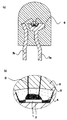
On the other hand, as a semiconductor light emitting device that emits various emission colors by a single light emitting element by combining an LED chip that emits a monochromatic peak wavelength and a fluorescent material, Japanese Patent Laid-Open No. 5-152609 (Patent Document 1) or Those described in JP-A-7-99345 (Patent Document 2) and the like are known. FIG. 4A is a schematic diagram showing an example of such a semiconductor device. In these semiconductor light emitting devices, the LED chip 1 having a relatively large energy band gap in the light emitting layer is disposed on a cup provided at the tip of a lead frame composed of a pair of
[0004]
For the color conversion member 4 used in the semiconductor light emitting device, the translucent resin used as the base material of the
[0005]
As these epoxy resins, it has been proposed to use an epoxy resin composition mainly composed of an alicyclic epoxy resin and cured with an acid anhydride. An epoxy resin cured with an acid anhydride-based curing agent is excellent in translucency and light resistance. For example, JP 2000-196151 A (Patent Document 3) discloses a mold resin mainly composed of an alicyclic epoxy resin in place of a general bisphenol type epoxy resin. An epoxy resin composition mainly composed of an alicyclic epoxy resin and cured with an acid anhydride has a long carbon irradiation because the main skeleton contains few carbon-carbon double bonds that cause photodegradation. Later, the mold resin is hardly deteriorated and is relatively excellent in flexibility, so that the semiconductor chip is hardly damaged by thermal stress.
[0006]
[Patent Document 1]
JP-A-5-152609
[Patent Document 2]
JP-A-7-99345
[Patent Document 3]
JP 2000-196151 A
[0007]
[Problems to be solved by the invention]
However, in the conventional light emitting device, the luminance is likely to change due to long-time use, and color unevenness is likely to occur. In particular, due to the dramatic progress of optical semiconductor technology today, optical semiconductor devices have been significantly increased in output and wavelength. For example, in light-emitting diodes using nitride semiconductors, the main components depend on the elements constituting the composition of the light-emitting layer. The emission peak can emit light at an arbitrary emission peak of about 365 nm to 650 nm, and a multi-quantum well structure is formed in a nitride semiconductor light emitting layer even with visible light of 550 nm or less (specifically, near ultraviolet light to blue-green light). By using it, a high output of 5 mW or more can be emitted. In such an optical semiconductor device capable of emitting or receiving high-energy light, changes in luminance and color unevenness are particularly likely to occur.
[0008]
SUMMARY OF THE INVENTION An object of the present invention is to provide a light emitting device that can emit light uniformly and with high brightness over a long period of time and has little color unevenness, and a method for forming the same.
[0009]
[Means for Solving the Problems]
As a result of various experiments, the present inventor has found that the deterioration of color and the uneven color in the small color conversion type light emitting device are due to the reliability of the
[0010]
First, the influence of the unreacted part in the epoxy resin will be described. As an epoxy resin curing agent, for example, an acid anhydride curing agent is often used from the viewpoint of translucency and light resistance. However, since an acid anhydride curing agent requires a relatively long curing time, it tends to absorb moisture and volatilize during curing. Further, in the color conversion type light emitting device in which the light emitting element 1 is sealed with a
[0011]
Epoxy resins that have caused poor curing cannot exhibit the original performance of the resin, and the light resistance and heat resistance are greatly reduced. Moreover, if the unreacted part remains, not only the original properties of the resin are deteriorated, but the unreacted part easily absorbs ultraviolet light or near ultraviolet light (blue), and thereby yellowing coloring appears remarkably. . The yellowing of the resin causes a color balance shift and color unevenness of the semiconductor light emitting device. In particular, in the case of a light emitting device in which a semiconductor light emitting element and a phosphor are combined, poor curing of the epoxy resin in the color conversion member becomes a very serious problem. For example, in a light emitting device that emits white light by mixing blue light and yellow light, the white color balance is shifted when the epoxy resin of the color conversion member turns yellow. Since the human eye is more sensitive to a color shift of white than a single color, even a slight color shift due to yellowing of the epoxy resin becomes a big problem.
[0012]
Next, the influence of sedimentation of the fluorescent particles 4 inside the
[0013]
For example, when the fluorescent material 4 is contained in a liquid resin like a conventional epoxy resin, it is particularly difficult to obtain stable dispersibility because the fluorescent material 4 settles due to a difference in specific gravity. Therefore, in order to suppress sedimentation of the fluorescent substance 4, there is a method of potting while stirring with a filling device having a stirrer. However, with the downsizing of the light emitting device, the filling device has also been downsized. When the mixed solution is stirred with a stirrer, there is a risk that the inner wall of the instrument is damaged and the fragments are mixed into the resin, or the surface crystals of the fluorescent material are ground and adversely affect the optical properties. In addition, if the resin contains a dispersing agent such as a filler or a diffusing agent together with the fluorescent material, the dispersibility is improved to some extent, but if it is contained in a large amount in order to obtain sufficient dispersibility, the light extraction path is reduced and the output is reduced. Will fall.
[0014]
Therefore, the present invention uses a triazine derivative epoxy resin having a particularly fast curing speed among non-aromatic epoxy resins having excellent light resistance, and completes resin curing in a state where the curing agent is maintained at a substantially stoichiometric number. An optical semiconductor device that is excellent in reliability and can emit light uniformly by the technique is provided.
[0015]
That is, the light emitting device of the present invention Manufacturing method Is a light emitting element; A substrate having a cup on which the light emitting element is disposed; A fluorescent material capable of absorbing at least a part of light emitted from the light emitting element and emitting light having other wavelengths, and a color conversion member containing the fluorescent substance and covering the light emitting element; A mold member covering the color conversion member; Light emitting device having Manufacturing method In
The color conversion member, A dispersion solution is prepared by adding at least a triazine derivative epoxy resin as a powder and a fluorescent material in a curing solution containing an acid anhydride curing agent as a main component, and the mixed solution is poured into the cup and cured by heating. To form It is characterized by that. Since the triazine derivative epoxy resin has a high curing rate, even when a hardener that easily volatilizes, such as an acid anhydride, is used, residual unreacted parts due to a shortage of the hardener are suppressed. The triazine derivative epoxy resin of the present invention is , Hard Solid at room temperature before conversion ( Powder) and has an effect of assisting dispersion of the phosphor, and becomes a transparent resin after curing. Therefore, according to the present invention, it is possible to obtain a light-emitting device that has excellent optical characteristics and high reliability by suppressing insufficient resin curing in the color conversion member and sedimentation of the phosphor.
[0016]
The triazine derivative epoxy resin is preferably an epoxy resin which is a derivative of a 1,3,5-triazine nucleus. In particular, an epoxy resin having an isocyanurate ring is excellent in light resistance and assists the dispersion of the phosphor well. 2 for one isocyanurate ring Base More preferably 3 Base It is desirable to have the epoxy group.
[0017]
Moreover, in the said color conversion member, the light resistance and toughness of a color conversion member improve by hardening | curing a triazine derivative epoxy resin with an acid anhydride hardening | curing agent. The content ratio of the triazine derivative epoxy resin and the acid anhydride curing agent is preferably 100: 80 to 100: 240, whereby a light emitting device with further excellent reliability can be obtained.
[0018]
Further, the semiconductor light emitting device of the present invention Manufacturing A method comprising: a light emitting device; A substrate having a cup on which the light emitting element is disposed; A fluorescent material capable of absorbing at least a part of light emitted from the light emitting element and emitting light having other wavelengths, and a color conversion member containing the fluorescent substance and covering the light emitting element; A mold member covering the color conversion member; In a method for forming a light-emitting device having a resin composition, a powdered resin is added to a curing solution containing an acid anhydride curing agent as a main component at a temperature lower than the melting point of the resin to prepare a mixed solution. Add a powdered fluorescent substance to the solution and distribute it uniformly. Scattered First step and the dispersion obtained in the first step Pour into the cup A second step of forming a color conversion member by coating the light emitting element and then heating to a temperature equal to or higher than the melting point of the resin to cure the dispersion solution.
[0019]
According to the forming method of the present invention, since the powder resin assists the dispersion of the phosphor particles, a color conversion member in which the phosphor is well dispersed can be obtained. Therefore, a light emitting device capable of maintaining uniform light for a long time regardless of the shape and particle size of the fluorescent material can be easily realized.
[0020]
The resin as the powder is opaque and preferably has translucency after being cured in the second step. Thereby, the handling of the resin is easy, and the dispersion state of the fluorescent substance can be grasped when the dispersion solution is prepared and the light emitting element is directly coated with the dispersion solution. Further, it can be easily confirmed whether or not the reaction between the resin and the curing agent is completed.
[0021]
The resin as the powder is preferably a triazine derivative epoxy resin, particularly an epoxy resin having an isocyanurate ring. The triazine derivative epoxy resin undergoes a curing reaction at a very high rate when heated to a melting point or higher and becomes a liquid. Therefore, a color conversion part agent is made into a thin film by using a highly volatile curing agent such as an acid anhydride curing agent. Even when it is applied, insufficient curing of the resin can be prevented. Therefore, a highly reliable light-emitting device in which the content ratio between the epoxy resin and the acid anhydride curing agent is close to the stoichiometric number can be formed. In addition, in order to compensate for volatilization of the acid anhydride curing agent, an acid anhydride in excess of the stoichiometric number of the epoxy compound to be cured may be included in the curing solution.
[0022]
DETAILED DESCRIPTION OF THE INVENTION
Hereinafter, embodiments of the present invention will be described with reference to the drawings.
FIG. 1A is a schematic cross-sectional view showing an example of a semiconductor light emitting device according to an embodiment of the present invention, and FIG. 1B is a partial enlarged cross-sectional view of FIG. An LED chip 1 having a relatively large energy band gap in the light emitting layer is fixed by a
[0023]
The
[0024]
The
(1) First, a triazine derivative epoxy resin, which is a powder, is added to a curing solution containing an acid anhydride curing agent as a main component at a temperature lower than the melting point of the resin to prepare a mixed solution. A yellow powder fluorescent material is added to the solution and dispersed uniformly to prepare a coating solution (= epoxy resin composition). Since the triazine derivative epoxy resin used in the present invention is typically a white powder, the coating liquid before curing is generally white.
(2) Next, after covering the LED chip 1 with the obtained coating solution, the LED chip 1 is heated to a temperature equal to or higher than the melting point of the triazine derivative epoxy resin, and the
[0025]
As described above, when the curing agent and the fluorescent substance are contained and dispersed in the resin having the triazine derivative epoxy resin at a temperature lower than the melting point, the triazine derivative epoxy resin serves as a dispersant, and the fluorescent substance is precipitated. Can be suppressed. The dispersion solution thus preferably dispersed is placed directly on the light emitting element while keeping the temperature constant, and then the triazine derivative epoxy resin of the powder is liquefied and rapidly reacted with the curing agent in an environment of the melting point or higher. Thus, the triazine derivative epoxy resin can be changed to a translucent solid while maintaining the dispersibility of the fluorescent substance. Therefore, color unevenness can be improved without impairing light extraction efficiency. Furthermore, the viscosity of the curing solution coexisting with the powder resin is less than that when coexisting with the liquid resin, and the liquefied triazine derivative epoxy resin undergoes a rapid curing reaction. The amount made can be limited and the resin can be cured well.
[0026]
In addition, it is also possible to harden | cure, leaving the particle-like morphology of a powder epoxy resin to some extent by selecting the temperature at the time of hardening suitably. For example, an interface where light is scattered is formed inside the
[0027]
In the color conversion member, the content ratio of the triazine derivative epoxy resin and the curing agent is preferably 100: 80 to 100: 240. When the curing agent is contained in a larger amount than the above range, the unreacted curing agent remains in the resin, and the moisture resistance of the light emitting element is deteriorated. When the curing agent is less than the above range, it takes a long time to melt and cure all of the triazine derivative epoxy resin, and it becomes difficult to fix the phosphor while maintaining the dispersibility of the fluorescent material. Moreover, poor curing occurs and the reliability of the resin is deteriorated.
[0028]
Hereinafter, each configuration will be described in detail.
(Triazine derivative epoxy resin)
The triazine derivative epoxy resin is preferably an epoxy resin which is a derivative of a 1,3,5-triazine nucleus. For example, it is an epoxy resin having a structure in which an epoxy group is added to any one of nitrogen atoms at the 1, 3, and 5 positions of a 1,3,5-triazine nucleus. In particular, an epoxy resin having an isocyanurate ring is excellent in light resistance and assists the dispersion of the phosphor well. A structure in which hydrogen bonded to nitrogen at
[0029]
The triazine derivative epoxy resin is a powder resin, and has a melting point of 100 ° C. to 115 ° C. when used alone and a high melting point of 80 ° C. to 100 ° C. even when mixed with a curing solution. In addition, it is stable and not reactive when in a powder state, but has rapid reactivity when liquefied and has translucency after curing. In the present invention, focusing on the above characteristics of the triazine derivative epoxy resin, the color conversion member formed by directly covering the light emitting element contains the triazine derivative epoxy resin, thereby realizing a light emitting device that suppresses uneven color and has little deterioration in the process. To do.
[0030]
(Curing agent)
In the present invention, an acid anhydride is preferably used as the curing agent. In particular, one or two kinds of polybasic acid carboxylic acid anhydrides that are non-aromatic and chemically do not have a carbon double bond are preferred because light resistance is required. Specific examples include hexahydrophthalic anhydride, methylhexahydrophthalic anhydride, trialkyltetrahydrophthalic anhydride, and hydrogenated methylnadic acid anhydride. In particular, it is preferable to use methylhexahydrophthalic anhydride having a good balance between curing reactivity and moisture resistance as the acid anhydride. These acid anhydrides have high volatility, but when combined with the above-mentioned triazine derivative epoxy resin, it is possible to suppress the occurrence of poor curing due to insufficient curing agent.
[0031]
On the other hand, although a cationic curing agent such as an aromatic sulfonium salt having low volatility can be used, since the epoxy resin cured by the cationic curing agent is easily irradiated with short wavelength light because it easily absorbs short wavelength light below blue. Easy to cause yellowing. Therefore, when an epoxy resin composition cured with a cationic curing agent is used in an optical semiconductor device that emits or receives light having a short wavelength of blue or less, the resin is yellowed and light emission unevenness is likely to occur. In particular, in the case of a color conversion type light emitting device having a fluorescent material, the light is confined with high density by the fluorescent material precipitated around the light emitting element, and yellowing tends to be remarkable.
[0032]
In addition, since the curing reaction with the cationic curing agent proceeds almost only by the ring-opening reaction between the epoxy groups, the obtained epoxy resin composition has a three-dimensional network structure in which ether bonds are relatively regularly arranged. And low flexibility. For this reason, when a light emitting element electrically connected with an epoxy resin cured by a cationic curing agent is directly covered, a large stress is likely to be generated between the light emitting chip and the resin during heating and cooling of the light emitting device.
[0033]
In order to improve the flexibility of the epoxy resin composition cured with a cationic curing agent, a low molecular weight reaction such as monoglycidyl ether, polyglycol giglycidyl ether, tertiary carboxylic acid monoglycidyl ether or the like is cured on the cured epoxy resin. It is also possible to mix a functional diluent. However, since mixing of these reactive diluents hinders the curing of the epoxy resin, it is necessary to increase the use amount of the cationic curing agent, which further aggravates the yellowing problem of the epoxy resin composition.
[0034]
(Cocatalyst)
The epoxy resin composition may contain a promoter. Alcohols and polyols that act as co-catalysts not only give flexibility to the cured product and improve the peel adhesion, but also function as a compatibilizer for the curing accelerator described later. Alcohols and polyols are also required to have light resistance, so they are non-aromatic and do not have a carbon double bond in chemical structure. They are straight-chain, branched, alicyclic, or ether group-containing types having 2 to 12 carbon atoms. Such alcohols and polyols are preferably used. Specific examples include propanol, isopropanol, methylcyclohexanol, ethylene glycol, glycerin, trimethylolpropane, and ethylene glycol monomethyl ether.
[0035]
Alcohols and polyols are also compatibilizers for curing accelerators, and are affected by the chemical structure and blending amount of the curing accelerator, but are preferably blended in a small amount of 1 to 30 parts by weight of a low molecular weight diol such as ethylene glycol, More preferred is 5 to 15 parts by weight.
[0036]
(Curing accelerator)
Moreover, you may make the said epoxy resin composition contain a hardening accelerator. As the curing accelerator, 1. Tertiary amines or imidazoles and / or their organic carboxylates; 2. 2. phosphines and / or quaternary salts thereof; 3. organic carboxylic acid metal salt; 4. metal-organic chelate compounds; An aromatic sulfonium salt is mentioned, It can use individually or in mixture of 2 or more types.
[0037]
Specific examples of tertiary amines, imidazoles and their organic carboxylates include 2,4,6-tris (diaminomethyl) phenol, 2-ethyl-4-methylimidazole, 1,8-diazabiscyclo (5,5). 4,0) Undecene-7 (hereinafter DBU) and its octylate. In particular, DBU octylate, which is excellent in translucency of the cured product, is preferably blended in an amount of 0.01 to 1 part by weight with respect to 100 parts by weight of the epoxy resin. More preferably, 5 parts by weight is blended.
[0038]
Specific examples of phosphines and quaternary salts thereof include triphenylphosphine, tributylphosphine, benzyltriphenylphosphonium bromine salt, and benzyltributylphosphonium bromine salt. In particular, it is preferable to blend 0.01 to 1 part by weight of benzyltriphenylphosphonium bromine salt, which is excellent in translucency of the cured product, with respect to 100 parts by weight of the epoxy resin. More preferred is a blend of ˜0.5 parts by weight.
[0039]
Specific examples of the organic carboxylic acid metal salt include zinc octylate, zinc laurate, zinc stearate, tin octylate and the like that do not have a carbon double bond inferior in light resistance. The organic carboxylic acid metal salt is in proportion to the increase in the carbon number of the organic carboxylic acid component, and the solubility in the epoxy resin decreases. Zinc octylate has the widest blending amount, and since it is liquid, it does not require time for dispersion and dissolution. Therefore, it is preferable to blend 1 to 10 parts by weight of zinc octylate from the viewpoint of curability. Considering the translucency of the cured product, 1 to 5 parts by weight is more preferable.
[0040]
Specific examples of the metal-organic chelate compound include acetylacetone zinc chelate, benzoylacetone zinc chelate, dibenzoylmethane zinc chelate, and ethyl zinc acetoacetate chelate composed of zinc and β-diketone which do not affect translucency. In particular, by using a zinc chelate compound, excellent light resistance and heat resistance can be imparted to the epoxy resin. In addition, since the zinc chelate compound has a selective and gentle curing accelerating action on the epoxy resin, low-stress adhesion is possible even with a low molecular weight monomer such as an alicyclic epoxy resin as a main component. Zinc chelate compound is bis (acetylacetonato) aqua zinc (2) [Zn (C 5 H 7 O 2 ) 2 (H 2 O)] is preferably blended in an amount of 1 to 10 parts by weight, and more preferably 1 to 5 parts by weight in consideration of solubility in an epoxy resin.
[0041]
The aromatic sulfonium salt is used in an epoxy resin single composition that does not contain an acid anhydride as a curing agent in the composition. The aromatic sulfonium salt is decomposed by heat and / or ultraviolet light of 360 nm or less to generate cations, and an epoxy resin cationic polymerization cured product can be obtained. The obtained cured product is ether-crosslinked and is more physically and chemically more stable than the cured product of the curing agent. Specific examples include triphenylsulfonium hexafluoride antimony salt and triphenylsulfonium hexafluoride phosphorous salt. In particular, triphenylsulfonium hexafluoride antimony salt has a high curing rate and can be sufficiently cured even in a small amount, so that 0.01 to 0.5 parts by weight is preferable with respect to 100 parts by weight of the epoxy resin. In consideration of discoloration, 0.05 to 0.3 parts by weight is more preferable.
[0042]
(Antioxidant)
The epoxy resin composition may contain an antioxidant. Antioxidants include: Phenolic (antioxidant), 2. 2. Phosphite system (antioxidant); Sulfur-based (antioxidant) can be mentioned, and can be used alone or in combination of two or more. By using two or more types in combination, for example, a synergistic effect is obtained by a combination of a phenol type and a phosphite type, or a phenol type and a sulfur type, and an initial coloration preventing effect and a thermal deterioration suppressing effect are improved. Specific examples of phenolic antioxidants include 2,6-di-tert-butyl-p-cresol, pentaerythritol, octadecyl-3- (3,5-di-tert-butyl-4-hydroxyphenyl) propionate, etc. What is blended is preferably 0.01 to 2 parts by weight with respect to 100 parts by weight of the epoxy resin, more preferably 0.1 to 0.5 parts by weight. Property is improved. Specific examples of phosphite antioxidants include triphenyl phosphite, 2,2-methylenebis (4,6-di-tert-butylphenyl) octyl phosphite, and 9,10-dihydro-9-oxa-10. -Phosphaphenanthrene-10-oxide and the like, and 0.01 to 10 parts by weight of 100 parts by weight of the epoxy resin can prevent initial coloration of the cured product, while 0.1% Addition of ˜2 parts by weight can improve the moisture resistance of the light emitting diode. Specific examples of sulfur-based antioxidants include dilauryl thiodipropionate, distearyl thiodipropionate, and the like is preferably a blend of 0.01 to 5 parts by weight with respect to 100 parts by weight of epoxy resin. More preferably, it is blended in an amount of 0.1 to 2 parts by weight, whereby the moisture resistance of the cured product can be improved.
[0043]
(Diluent)
Moreover, you may add a diluent to the said epoxy resin composition. Diluents include non-reactive and reactive types. Examples of the reactive type include higher alcohol glycidyl ether, diepoxide, triepoxide and the like. What mix | blended 3-10 weight part of these diluents with respect to 100 weight part of epoxy resins is preferable, and can ensure workability | operativity by this.
[0044]
(Fluorescent substance)
The phosphor used in the light emitting device of the present invention is a cerium-activated yttrium / aluminum oxide phosphor capable of emitting light by exciting light emitted from a semiconductor light emitting element having a nitride semiconductor as a light emitting layer. It is based. As a specific yttrium / aluminum oxide fluorescent material, YAlO 3 : Ce, Y 3 Al 5 O 12 Y: Ce (YAG: Ce) or Y 4 Al 2 O 9 : Ce, and also a mixture thereof. The yttrium / aluminum oxide fluorescent material may contain at least one of Ba, Sr, Mg, Ca, and Zn. Moreover, by containing Si, the reaction of crystal growth can be suppressed and the particles of the fluorescent material can be aligned. In this specification, the yttrium / aluminum oxide phosphor activated by Ce is to be interpreted in a broad sense, and a part or all of yttrium is selected from the group consisting of Lu, Sc, La, Gd and Sm. Or a part or the whole of aluminum is used in a broad sense including a fluorescent substance having a fluorescent action in which any one or both of Ba, Tl, Ga, and In are substituted.
[0045]
More specifically, the general formula (Y z Gd 1-z ) 3 Al 5 O 12 : Photoluminescence phosphor represented by Ce (where 0 <z ≦ 1) or a general formula (Re 1-a Sm a ) 3 Re ' 5 O 12 : Ce (where 0 ≦ a <1, 0 ≦ b ≦ 1, Re is at least one selected from Y, Gd, La, Sc, and Re ′ is at least one selected from Al, Ga, In) The photoluminescence phosphor shown in FIG. Since this fluorescent material has a garnet structure, it is resistant to heat, light, and moisture, and the peak of the excitation spectrum can be made around 450 nm. In addition, the emission peak is in the vicinity of 580 nm and has a broad emission spectrum that extends to 700 nm. Further, the photoluminescence phosphor can increase the excitation light emission efficiency in a long wavelength region of 460 nm or more by containing Gd (gadolinium) in the crystal. As the Gd content increases, the emission peak wavelength shifts to a longer wavelength, and the entire emission wavelength also shifts to the longer wavelength side. That is, when a strong reddish emission color is required, it can be achieved by increasing the amount of Gd substitution. On the other hand, as Gd increases, the emission luminance of photoluminescence by blue light tends to decrease. Furthermore, in addition to Ce, Tb, Cu, Ag, Au, Fe, Cr, Nd, Dy, Co, Ni, Ti, Eu, and the like can be contained as desired. Moreover, in the composition of the yttrium / aluminum / garnet phosphor having a garnet structure, the emission wavelength is shifted to the short wavelength side by replacing a part of Al with Ga. Further, by substituting part of Y in the composition with Gd, the emission wavelength is shifted to the longer wavelength side. When substituting a part of Y with Gd, it is preferable that the substitution with Gd is less than 10%, and the Ce content (substitution) is 0.03 to 1.0. If the substitution with Gd is less than 20%, the green component is large and the red component is small. However, by increasing the Ce content, the red component can be supplemented and a desired color tone can be obtained without lowering the luminance. With such a composition, the temperature characteristics are good and the reliability of the light emitting diode can be improved. In addition, when a photoluminescent phosphor adjusted to have a large amount of red component is used, a light emitting device capable of emitting an intermediate color such as pink can be formed. Such photoluminescent phosphors use oxides or compounds that easily become oxides at high temperatures as raw materials for Y, Gd, Al, and Ce, and mix them well in a stoichiometric ratio. Get raw materials. Alternatively, a mixed raw material obtained by mixing a coprecipitation oxide obtained by firing a solution obtained by coprecipitation of a solution obtained by dissolving a rare earth element of Y, Gd, and Ce in an acid in a stoichiometric ratio with oxalic acid and aluminum oxide. Get. A suitable amount of fluoride such as barium fluoride or ammonium fluoride is mixed as a flux and packed in a crucible, and fired in air at a temperature range of 1350 to 1450 ° C. for 2 to 5 hours to obtain a fired product, and then fired. The product can be obtained by ball milling in water, washing, separating, drying and finally passing through a sieve.
[0046]
In the light emitting device of the present invention, such a photoluminescent phosphor may be a mixture of yttrium / aluminum / garnet phosphor activated by two or more kinds of cerium and other phosphors. By mixing two types of yttrium / aluminum / garnet phosphors with different amounts of substitution from Y to Gd, light having a desired color tone can be easily realized. In particular, the fluorescent material with a large amount of substitution is a large particle size fluorescent material, and the fluorescent material with a small or zero amount of substitution is a medium particle size fluorescent material having a smaller central particle size value than the large particle size fluorescent material. Then, improvement in color rendering and luminance can be realized at the same time.
[0047]
The particle size of the fluorescent material used in the present invention is preferably in the range of 10 μm to 50 μm, more preferably 15 μm to 30 μm. Thereby, concealment of light can be suppressed and the luminance of the integrated nitride semiconductor light emitting device can be improved. In addition, the fluorescent material having the above particle size range has a high light absorption rate and conversion efficiency and a wide excitation wavelength range. Since the color conversion member of the present invention mixes and disperses the powder resin and the fluorescent material, the color conversion member can be obtained while uniformly dispersing the large particle size fluorescent material having such optically superior characteristics. A light-emitting device that can be formed and can emit light with high luminance with high reliability can be formed. On the other hand, a fluorescent material having a particle size smaller than 15 μm is relatively easy to form an aggregate, tends to be densely settled in the liquid resin, and reduces the light transmission efficiency. Here, in the present invention, the particle size is a value obtained from a volume-based particle size distribution curve. The volume-based particle size distribution curve is obtained by measuring the particle size distribution by a laser diffraction / scattering method. Specifically, in an environment of an air temperature of 25 ° C. and a humidity of 70%, hexametalin having a concentration of 0.05%. Each substance was dispersed in an aqueous sodium acid solution and measured with a laser diffraction particle size distribution analyzer (SALD-2000A) in a particle size range of 0.03 μm to 700 μm. If the particle size value when the integrated value is 50% in this volume-based particle size distribution curve is defined as the center particle size, the center particle size of the fluorescent material used in the present invention is preferably in the range of 15 μm to 50 μm. Moreover, it is preferable that the fluorescent substance which has this center particle size value is contained frequently, and the frequency value is preferably 20% to 50%. In this way, by using a fluorescent material with small variation in particle size, a light emitting device having a favorable color tone with suppressed color unevenness can be obtained. In addition, when a small particle size fluorescent material having a central particle size of 0.3 μm or more and less than 1 μm is included, these fluorescent materials hardly emit light, but the luminous intensity is lower than when other diffusing agents are used. In addition, the resin viscosity can be adjusted without causing the light to diffuse and light can be more uniformly emitted.
[0048]
(Diffusion agent)
Further, in the present invention, the color conversion member may contain a diffusing agent in addition to the fluorescent material. As a specific diffusing agent, barium titanate, titanium oxide, aluminum oxide, silicon oxide or the like is preferably used. As a result, a light emitting device having good directivity can be obtained.
In this specification, the diffusing agent preferably has a center particle size of 0.3 nm or more and less than 5 μm, more preferably 0.3 μm or more and less than 1.0 μm. Such a diffusing agent is preferable because it diffuses light from the light emitting element and the fluorescent material well and can suppress color unevenness that tends to occur by using a fluorescent material having a large particle size. In addition, the half width of the emission spectrum can be narrowed, and a light emitting device with high color purity can be obtained. A diffusing agent having a size of 0.3 μm or more and less than 1 μm has a low interference effect on the light wavelength from the light emitting element, but can adjust the resin viscosity without reducing the luminous intensity. As a result, when the color conversion member is arranged by potting or the like, it becomes possible to disperse the fluorescent substance in the resin almost uniformly in the syringe and maintain the state, and the fluorescent substance having a large particle size that is relatively difficult to handle. Even when a substance is used, it is possible to produce with good yield. In addition, as described above, the diffusing agent in the present invention has a different action depending on the particle size range, and can be selected or combined according to the method of use.
[0049]
(Mount member)
The mount member used in the present invention has a semiconductor light-emitting element and a substrate with high mass productivity. Body and And an epoxy resin composition that suppresses deterioration due to a light emission wavelength from a semiconductor light emitting element or the like. Such an epoxy resin composition can contain a curing agent, a co-catalyst, and a curing accelerator in addition to the alicyclic epoxy resin and the acid anhydride. Needless to say, the light resistance, heat resistance and adhesiveness can be variously adjusted according to the chemical structure and blending amount of each component. Moreover, it can also be used as an electrically conductive paste by including Ag, Au, ITO, etc. in an epoxy resin composition.
[0050]
(Substrate)
Groups used in the present invention Body and Is a device in which a semiconductor light emitting element is arranged, and it can be effectively used by reflecting the emission wavelength from the semiconductor light emitting element. Accordingly, it is sufficient that the size is sufficient for bonding with the mount member, and various shapes and materials can be used as desired. Specifically, lead terminals used for light-emitting diodes, chip-type LED packages, and the like are preferably used.
[0051]
One semiconductor light emitting element may be disposed on the substrate, or two or more semiconductor light emitting elements may be disposed. In addition, an LED chip having a plurality of emission wavelengths can be arranged to adjust the emission wavelength. When an LED chip or the like using a nitride semiconductor formed on SiC is disposed, sufficient electrical conductivity is required as well as adhesiveness. Moreover, when connecting the electrode of a semiconductor light emitting element with the lead electrode etc. which become a board | substrate using a conductive wire, it is preferable that connectivity with a conductive wire etc. is good. Specific examples of such substrates include lead electrodes, packages, etc., such as iron, copper, iron-containing copper, tin-containing copper, copper-gold silver, and other materials such as aluminum and iron, and ceramics and various synthetic resins. Can be formed into various shapes.
[0052]
(Conductive wire)
The conductive wire that is an electrical connection member is required to have good ohmic properties, mechanical connectivity, electrical conductivity, and thermal conductivity with the electrodes of the semiconductor light emitting device. The thermal conductivity is 0.01 cal / cm 2 / Cm / ° C. or higher is preferable, and more preferably 0.5 cal / cm 2 / Cm / ° C. or higher. In consideration of workability and the like, the diameter of the conductive wire is preferably Φ10 μm or more and Φ45 μm or less. Specific examples of such conductive wires include conductive wires using metals such as gold, copper, platinum, and aluminum, and alloys thereof. Such a conductive wire can easily connect the electrode of each LED chip to the inner lead, the mount lead, and the like by a wire bonding device.
[0053]
(Mold member)
The mold member is provided to protect the semiconductor light emitting element and the like from the external environment. Therefore, the color conversion member can be used as it is as a mold member, or a translucent resin can be formed separately from the color conversion member to form a mold member. Such a mold member can utilize various forms as desired, such as a convex lens shape and a concave lens shape. The mold member that is not in contact with the semiconductor light emitting element can use various translucent resins, but the mold resin that is in contact with the semiconductor light emitting element is the same as the base material of the mount resin and color conversion member of the present invention. It is preferable to use an epoxy resin composition.
[0054]
More specifically, the translucent resin constituting the mold resin is preferably an alicyclic epoxy resin composition having an aromatic component of 5 wt% or less (including the case where no aromatic epoxy resin is contained). An alicyclic epoxy resin composition that can have an inorganic chlorine content of 1 ppm or less and an organic chlorine content of 5 ppm or less is more preferable. As the translucent resin used for the mold member, an epoxy resin composition composed of an alicyclic epoxy resin and an acid anhydride is more preferable. Moreover, in addition to various diffusing materials and colorants, the above-mentioned various additives can also be contained.
[0055]
【Example】
Example 1
As the light emitting device of the present invention, a long wavelength conversion type lamp type light emitting diode as shown in FIGS. 1A and 1B is formed. As the LED chip, an LED chip having a light emitting layer made of InGaN and having a main light emission peak of 470 nm is used. The LED chip is formed using the MOCVD method. Specifically, a cleaned sapphire substrate is placed in the reaction chamber. Film formation using TMG (trimethyl) gas, TMI (trimethylindium) gas, TMA (trimethylaluminum) gas, ammonia gas and hydrogen gas as carrier gas, and silane gas and cyclopentadiamagnesium as impurity gas as reaction gas Let
[0056]
As the layer structure of the LED chip 1, AlGaN as a low-temperature buffer layer on a sapphire substrate, non-doped GaN (thickness about 15000 mm) for improving crystallinity, and Si-doped GaN (thickness) having an electrode formed and serving as an n-type contact layer About 21650 mm), comprising a superlattice of non-doped GaN (thickness about 3000 mm) for improving crystallinity, non-doped GaN (thickness about 50 mm) as an n-type cladding layer, and Si-doped GaN (thickness about 300 mm) Multilayer film, multilayer film composed of a superlattice of non-doped GaN (thickness: about 40 mm) and non-doped InGaN (thickness: about 20 mm), which improves the crystallinity of the light emitting layer formed thereon, and a multiple quantum well structure As a light emitting layer composed of a multilayer film of non-doped GaN (thickness of about 250 mm) and InGaN (thickness of about 30 mm), p-type A multilayer film composed of a superlattice of Mg-doped InGaN (thickness: about 25 mm) and Mg-doped GaAlN (thickness: about 40 mm), and a p-type contact layer, Mg-doped GaN ( (A GaN layer is formed on the sapphire substrate at a low temperature to form a buffer layer. The p-type semiconductor is annealed at 400 ° C. or higher after the film formation.) ). Next, the surface of each pn contact layer is exposed on the same side as the nitride semiconductor on the sapphire substrate by etching. Positive and negative electrodes are formed on each contact layer by sputtering. . After drawing the scribe line on the completed semiconductor wafer, the semiconductor wafer is divided by an external force to form LED chips as light emitting elements. This LED chip has a monochromatic peak wavelength at 470 nm. Finally, an insulating protective film made of SiO.sub.2 is formed with a film thickness of 2 .mu.m so that the light transmittance is 90% at a wavelength of 470 nm so as to expose only the bonding surfaces of the electrodes and cover the entire element.
[0057]
Using a pair of
[0058]
Here, the
[0059]
Although various mount resins can be used, 3,4 epoxycyclomethyl-3 ′, 4 ′ epoxycyclohexylcarboxylate 100, which is a non-aromatic epoxy resin, as a more reliable epoxy resin composition. Uniform colorless and transparent by mixing 90 parts by weight of methylhexahydrophthalic anhydride, 10 parts by weight of ethylene glycol, 4 parts by weight of zinc octylate and 2.5 parts by weight of bis (acetylacetonato) aqua zinc (2) It is preferable to use an epoxy resin composition.
[0060]
Next, the positive and negative electrodes of the LED chip 1, the mount lead and the inner lead are wire-bonded with a gold wire to establish electrical continuity.
[0061]
Subsequently, 100 parts by weight of methylhexahydrophthalic anhydride, 2 parts by weight of ethylene glycol serving as a co-catalyst, and 0.5 parts by weight of benzyltriphenylphosphonium bromine salt are mixed to prepare a colorless and transparent cured solution.
[0062]
Next, to 328.32 parts by weight of the above-mentioned curing solution, 100 parts by weight of 1,3,5 triglycidyl isoannulate which is a triazine derivative epoxy resin having a melting point of 100 ° C. 1: 2) is mixed at room temperature to prepare a mixed solution.
[0063]
On the other hand, as the fluorescent material 4, Y is substituted by about 20% with Gd, and the center particle diameter is 21.429 μm (Y 0.8 Gd 0.2 ) 2.965 Al Five O 12 : Ce0.035 is formed. The fluorescent material is composed of a large particle size fluorescent material and a small particle size fluorescent material, and the flat region where the slope is zero in the volume standard distribution curve is an integrated value of 4.6% and a particle size range of 1.371 μm to 8 379 μm. That is, 4.6% of the total fluorescent material is made of a small particle size fluorescent material having a particle size smaller than 1.371 μm, and the remaining 95.6% is made of a large particle size fluorescent material having a particle size larger than 8.379 μm. Become. The center particle diameter of the fluorescent material classified by the sedimentation method so as to have such a distribution is 21.4 μm, and the frequency value at the center particle diameter is 29.12%. The frequency peak particle size value of the small particle size fluorescent material is 0.613 μm, and the frequency peak particle size value of the large particle size fluorescent material is 22.908 μm.
[0064]
In the CIE chromaticity table, the weight ratio of the powder fluorescent material thus adjusted and the mixed solution was 28:28 so that light with x, y = (0.33, 0.33) was obtained. Mix to 100 and disperse uniformly with a ball mill for 24 hours. The dispersion solution thus obtained is potted with a syringe in a concave portion of a housing in which an LED chip is connected to a pair of lead electrodes with a gold wire, preheated to 170 ° C., and cured in an oven for 2 hours. In this way, the
[0065]
Next, a liquid epoxy resin composition is injected into a casting case, which is a shell-shaped formwork, and a part of the mount lead and the inner lead in which the above-described LED chip is arranged in the cup is inserted into the casting case. Primary curing is performed at 120 ° C. for 2 hours. After the primary curing, the light emitting diode is extracted from the casting case, and the secondary curing is performed at 140 ° C. for 4 hours to form the
[0066]
In the light-emitting diode thus obtained, a fluorescent material layer in which many fluorescent materials are well dispersed and settled around the light-emitting element is very thin, so that high output and uniform light emission can be obtained. Moreover, the result of having investigated the initial relative output and energization time at the time of 20 mA energization is shown in FIG. There is almost no decrease in the light emission output when 1000 hours have elapsed, and the light emission output can be held until 3500 hours have elapsed.
[0067]
(Comparative example)
FIG. 5 shows the results of examining the initial relative output and energization time at the time of 20 mA energization in the light-emitting diode in the same manner as in Example 1 except that an epoxy resin that is a liquid resin at room temperature is used instead of the triazine derivative epoxy resin. Show. It decreases to 87% after 500 hours and to 78% after 1000 hours, resulting in color misregistration and color unevenness.
[0068]
(Example 2)
100 parts by weight of 1,3,5 triglycidyl isoannulate, which is a triazine derivative epoxy resin as a main agent, and 328.32 parts by weight of the above-mentioned curing solution (triazine derivative epoxy resin: curing solution = 1: 2 by epoxy equivalent ratio) In a mixed solution containing the above, the fluorescent material, and SiO having a center particle diameter of 0.5 μm. 2 When a light emitting diode is formed in the same manner as in Example 1 except that a dispersion obtained by uniformly dispersing in a ball mill for 24 hours is used, except that a weight ratio of 100: 23: 35 is mixed. As shown in FIG. 5, the same effect as in the first embodiment can be obtained.
[0069]
(Example 3) In a liquid in which 100 parts by weight of 1,3,5-triglycidyl isocyanurate, which is a triazine derivative epoxy resin as a main ingredient, and 328.32 parts by weight of a curing agent were mixed, phosphor and SiO 2 A light-emitting diode was prepared in the same manner as in Example 1 except that the resin was obtained by mixing so that the weight part of the diluent was 100: 23: 35: 10 and uniformly dispersed in a ball mill for 24 hours. When formed, the same effect as in Example 1 was obtained.
[0070]
【The invention's effect】
In the light emitting device of the present invention, a color conversion member containing a fluorescent material and directly covering the light emitting element contains at least a triazine derivative epoxy resin, so that a light emitting device having excellent optical characteristics and high reliability can be produced with high productivity. Obtainable.
[0071]
In addition, the method for forming a light emitting device of the present invention maintains a state in which a fluorescent material is well dispersed in a mixed solution by using a mixed solution in which a powdery resin and a fluorescent material are dispersed in a curing solution. It is possible to improve workability. Moreover, since it is not necessary to apply | coat on a light emitting element, stirring, there is no possibility that a foreign material will mix in a mixed solution, and each member can be arrange | positioned with high reliability. In addition, by producing a dispersion solution at a temperature lower than the melting point of the powder resin to be used and curing the dispersion solution applied at a temperature equal to or higher than the melting point, there is no color unevenness and a highly reliable color conversion type. A light emitting device can be realized.
[Brief description of the drawings]
FIGS. 1A and 1B are schematic cross-sectional views showing a light-emitting diode according to the present invention.
FIG. 2 is a reaction formula showing an example of a reaction between a triazine derivative epoxy resin and an acid anhydride curing agent.
FIG. 3 is a process diagram showing a method for forming a color conversion member according to the present invention.
4 (a) and 4 (b) are schematic cross-sectional views showing a conventional light emitting diode.
FIG. 5 is a graph showing the relationship between the relative output and the energization time during 20 mA energization in Examples 1 and 2 and a comparative example.
[Explanation of symbols]
1. Light emitting element
2 ... Mount resin
3 ... Wire
4 ... Fluorescent material
5 ... Diffusion agent
6 ... Mold member
7a ... First lead
7b ... Second Lead
Claims (9)
前記色変換部材を、酸無水物硬化剤を主成分とする硬化溶液中に、粉体であるトリアジン誘導体エポキシ樹脂と蛍光物質とを少なくとも添加して分散溶液を作製し、該分散溶液を前記カップ内に注入し加熱硬化して形成することを特徴とする発光装置の製造方法。A light-emitting element, a substrate having a cup on which the light-emitting element is disposed, a fluorescent material capable of absorbing at least part of light emitted from the light-emitting element and emitting light having other wavelengths, and the fluorescence In a method of manufacturing a light emitting device comprising a color conversion member that contains a substance and covers the light emitting element , and a mold member that covers the color conversion member,
The color conversion member is prepared by adding at least a triazine derivative epoxy resin as a powder and a fluorescent material to a curing solution containing an acid anhydride curing agent as a main component, and preparing the dispersion solution. A method of manufacturing a light emitting device , wherein the method is formed by injecting into a resin and heat curing .
酸無水物硬化剤を主成分とする硬化溶液中に、粉体である樹脂を該樹脂の融点より低い温度下にて添加し混合溶液を作製し、該混合溶液に粉体の蛍光物質を添加し均一に分散させる第1の工程と、
前記第1の工程にて得られた分散溶液を前記カップに注入し前記発光素子を被覆した後、前記樹脂の融点以上の温度まで加熱し、前記分散溶液を硬化させて色変換部材を形成する第2の工程と
を有する発光装置の製造方法。A light-emitting element, a substrate having a cup on which the light-emitting element is disposed, a fluorescent material capable of absorbing at least part of light emitted from the light-emitting element and emitting light having other wavelengths, and the fluorescence In a method for forming a light emitting device, comprising: a color conversion member that contains a substance and covers the light emitting element ; and a mold member that covers the color conversion member.
A powdered resin is added to a curing solution containing an acid anhydride curing agent as a main component at a temperature lower than the melting point of the resin to prepare a mixed solution, and a powdered fluorescent substance is added to the mixed solution. a first step of uniformly distributed,
The dispersion solution obtained in the first step is poured into the cup to cover the light emitting element, and then heated to a temperature equal to or higher than the melting point of the resin to cure the dispersion solution to form a color conversion member. A method for manufacturing a light emitting device including the second step.
Priority Applications (1)
| Application Number | Priority Date | Filing Date | Title |
|---|---|---|---|
| JP2002319485A JP4250949B2 (en) | 2001-11-01 | 2002-11-01 | Light emitting device and manufacturing method thereof |
Applications Claiming Priority (3)
| Application Number | Priority Date | Filing Date | Title |
|---|---|---|---|
| JP2001336944 | 2001-11-01 | ||
| JP2001-336944 | 2001-11-01 | ||
| JP2002319485A JP4250949B2 (en) | 2001-11-01 | 2002-11-01 | Light emitting device and manufacturing method thereof |
Publications (3)
| Publication Number | Publication Date |
|---|---|
| JP2003224305A JP2003224305A (en) | 2003-08-08 |
| JP2003224305A5 JP2003224305A5 (en) | 2005-12-22 |
| JP4250949B2 true JP4250949B2 (en) | 2009-04-08 |
Family
ID=27759058
Family Applications (1)
| Application Number | Title | Priority Date | Filing Date |
|---|---|---|---|
| JP2002319485A Expired - Lifetime JP4250949B2 (en) | 2001-11-01 | 2002-11-01 | Light emitting device and manufacturing method thereof |
Country Status (1)
| Country | Link |
|---|---|
| JP (1) | JP4250949B2 (en) |
Families Citing this family (34)
| Publication number | Priority date | Publication date | Assignee | Title |
|---|---|---|---|---|
| JP4337574B2 (en) * | 2003-09-25 | 2009-09-30 | 日亜化学工業株式会社 | LIGHT EMITTING DEVICE AND METHOD FOR FORMING THE SAME |
| JP5262374B2 (en) * | 2004-11-30 | 2013-08-14 | 日亜化学工業株式会社 | RESIN MOLDED BODY, SURFACE MOUNTED LIGHT EMITTING DEVICE AND METHOD FOR PRODUCING THEM |
| JP2006193570A (en) * | 2005-01-12 | 2006-07-27 | Stanley Electric Co Ltd | Thermosetting resin composition, light-transmitting cured product prepared by thermally curing the composition, and light-emitting diode sealed with the cured product |
| KR101139891B1 (en) * | 2005-01-31 | 2012-04-27 | 렌슬러 폴리테크닉 인스티튜트 | Light emitting diode device having diffusedly reflective surface |
| JP4557824B2 (en) * | 2005-07-04 | 2010-10-06 | 株式会社東芝 | Light emitting device and manufacturing method thereof |
| US20100104794A1 (en) * | 2005-08-04 | 2010-04-29 | Shin-Etsu Chemical Co., Ltd. | Thermosetting epoxy resin composition and semiconductor device |
| CN101268559B (en) * | 2005-08-04 | 2010-11-17 | 日亚化学工业株式会社 | Light-emitting device, method for manufacturing same, molded body and sealing member |
| WO2007135707A1 (en) | 2006-05-18 | 2007-11-29 | Nichia Corporation | Resin molded body and surface-mounted light emitting device, and manufacturing method thereof |
| JP5135735B2 (en) * | 2006-08-25 | 2013-02-06 | 日亜化学工業株式会社 | Light emitting device |
| JP2008144127A (en) * | 2006-11-15 | 2008-06-26 | Hitachi Chem Co Ltd | Thermosetting resin composition for light reflection, photosemiconductor element-loading substrate using the same, photosemiconductor device, and manufacturing process for the articles |
| KR101308263B1 (en) * | 2006-11-15 | 2013-09-13 | 히타치가세이가부시끼가이샤 | Heat curable resin composition for light reflection, process for producing the resin composition, and optical semiconductor element mounting substrate and optical semiconductor device using the resin composition |
| JP5380774B2 (en) | 2006-12-28 | 2014-01-08 | 日亜化学工業株式会社 | Surface mount type side surface light emitting device and manufacturing method thereof |
| JP5168152B2 (en) * | 2006-12-28 | 2013-03-21 | 日亜化学工業株式会社 | Light emitting device |
| JP5470680B2 (en) | 2007-02-06 | 2014-04-16 | 日亜化学工業株式会社 | LIGHT EMITTING DEVICE, MANUFACTURING METHOD THEREOF, AND MOLDED BODY |
| KR101309765B1 (en) * | 2007-03-29 | 2013-09-23 | 서울반도체 주식회사 | Light emitting diode with reduced chromatic deviation |
| JP5207658B2 (en) * | 2007-05-17 | 2013-06-12 | 日東電工株式会社 | Epoxy resin composition for sealing optical semiconductor element, cured product thereof, and optical semiconductor device using the same |
| JP4623322B2 (en) | 2007-12-26 | 2011-02-02 | 信越化学工業株式会社 | White thermosetting silicone resin composition for forming optical semiconductor case, optical semiconductor case and molding method thereof |
| JP5463447B2 (en) | 2008-01-18 | 2014-04-09 | 三洋電機株式会社 | Light emitting device and lamp provided with the same |
| JP4678415B2 (en) | 2008-03-18 | 2011-04-27 | 信越化学工業株式会社 | White thermosetting silicone resin composition for forming optical semiconductor case and optical semiconductor case |
| JP2010018786A (en) | 2008-06-09 | 2010-01-28 | Shin-Etsu Chemical Co Ltd | White heat-curable silicone resin composition for forming optical semiconductor case, and optical semiconductor case |
| JP2010021533A (en) | 2008-06-09 | 2010-01-28 | Shin-Etsu Chemical Co Ltd | White heat-curable silicone resin composition for forming optical semiconductor case, and optical semiconductor case |
| JP5218298B2 (en) | 2008-07-02 | 2013-06-26 | 信越化学工業株式会社 | Thermosetting silicone resin-epoxy resin composition and premolded package molded with the resin |
| JP5182512B2 (en) | 2008-12-15 | 2013-04-17 | 日亜化学工業株式会社 | Thermosetting epoxy resin composition and semiconductor device |
| JP5488326B2 (en) | 2009-09-01 | 2014-05-14 | 信越化学工業株式会社 | White thermosetting silicone epoxy hybrid resin composition for optical semiconductor device, method for producing the same, pre-mold package and LED device |
| JP5246880B2 (en) * | 2009-09-15 | 2013-07-24 | 信越化学工業株式会社 | Underfill material composition and optical semiconductor device |
| WO2011090269A2 (en) | 2010-01-19 | 2011-07-28 | Lg Innotek Co., Ltd. | Package and manufacturing method of the same |
| JP5650097B2 (en) | 2011-11-09 | 2015-01-07 | 信越化学工業株式会社 | Thermosetting epoxy resin composition and optical semiconductor device |
| KR101881604B1 (en) | 2011-11-21 | 2018-07-24 | 신에쓰 가가꾸 고교 가부시끼가이샤 | White thermosetting silicone resin composition useful as led reflector and optical semiconductor device using the same |
| JP5376014B2 (en) * | 2012-07-03 | 2013-12-25 | 日立化成株式会社 | A thermosetting resin composition for light reflection, an optical semiconductor mounting substrate using the same, a manufacturing method thereof, and an optical semiconductor device. |
| JP5725115B2 (en) * | 2013-09-25 | 2015-05-27 | ウシオ電機株式会社 | Light emitting device and lamp provided with the same |
| JP6194853B2 (en) | 2014-06-06 | 2017-09-13 | 信越化学工業株式会社 | White thermosetting silicone resin composition for optical semiconductor device and case for mounting optical semiconductor element |
| JP6311626B2 (en) | 2015-02-20 | 2018-04-18 | 信越化学工業株式会社 | White thermosetting epoxy resin composition for LED reflector |
| JP6809518B2 (en) * | 2018-08-28 | 2021-01-06 | 日亜化学工業株式会社 | Resin molded products and surface mount type light emitting devices and their manufacturing methods |
| JP7054019B2 (en) * | 2020-04-27 | 2022-04-13 | 日亜化学工業株式会社 | Resin molded body and surface mount type light emitting device and their manufacturing method |
-
2002
- 2002-11-01 JP JP2002319485A patent/JP4250949B2/en not_active Expired - Lifetime
Also Published As
| Publication number | Publication date |
|---|---|
| JP2003224305A (en) | 2003-08-08 |
Similar Documents
| Publication | Publication Date | Title |
|---|---|---|
| JP4250949B2 (en) | Light emitting device and manufacturing method thereof | |
| US6924596B2 (en) | Light emitting apparatus provided with fluorescent substance and semiconductor light emitting device, and method of manufacturing the same | |
| JP3428597B2 (en) | Optical semiconductor device and method of manufacturing the same | |
| JP4876426B2 (en) | Light emitting device with excellent heat resistance and light resistance | |
| KR100961324B1 (en) | Nitride Phosphor and Production Process Thereof, and Light Emitting Device | |
| JP4280038B2 (en) | Light emitting device | |
| JP2003179269A (en) | Optical semiconductor element | |
| JP5326182B2 (en) | Light emitting device, phosphor for light emitting element, and method for manufacturing the same | |
| JP3417415B1 (en) | Epoxy resin composition, method for producing the same, and optical semiconductor device using the same | |
| JP2007227791A (en) | Luminescent device manufacturing method and light emitting device manufactured thereby | |
| JP7053980B2 (en) | Light emitting device | |
| JP4017015B2 (en) | Light emitting device | |
| JP2009096947A (en) | Method for manufacturing phosphor-containing composition | |
| JP4725186B2 (en) | Light emitting device | |
| JP4009868B2 (en) | Nitride phosphor and light emitting device using the same | |
| JP2005019662A (en) | Light emitting device |
Legal Events
| Date | Code | Title | Description |
|---|---|---|---|
| A521 | Request for written amendment filed |
Free format text: JAPANESE INTERMEDIATE CODE: A523 Effective date: 20051101 Free format text: JAPANESE INTERMEDIATE CODE: A821 Effective date: 20051101 |
|
| A621 | Written request for application examination |
Free format text: JAPANESE INTERMEDIATE CODE: A621 Effective date: 20051101 |
|
| RD02 | Notification of acceptance of power of attorney |
Free format text: JAPANESE INTERMEDIATE CODE: A7422 Effective date: 20051101 |
|
| RD04 | Notification of resignation of power of attorney |
Free format text: JAPANESE INTERMEDIATE CODE: A7424 Effective date: 20051112 |
|
| RD03 | Notification of appointment of power of attorney |
Free format text: JAPANESE INTERMEDIATE CODE: A7423 Effective date: 20080131 |
|
| A977 | Report on retrieval |
Free format text: JAPANESE INTERMEDIATE CODE: A971007 Effective date: 20080701 |
|
| A131 | Notification of reasons for refusal |
Free format text: JAPANESE INTERMEDIATE CODE: A131 Effective date: 20080708 |
|
| A521 | Request for written amendment filed |
Free format text: JAPANESE INTERMEDIATE CODE: A523 Effective date: 20080908 |
|
| TRDD | Decision of grant or rejection written | ||
| A01 | Written decision to grant a patent or to grant a registration (utility model) |
Free format text: JAPANESE INTERMEDIATE CODE: A01 Effective date: 20081224 |
|
| A01 | Written decision to grant a patent or to grant a registration (utility model) |
Free format text: JAPANESE INTERMEDIATE CODE: A01 |
|
| A61 | First payment of annual fees (during grant procedure) |
Free format text: JAPANESE INTERMEDIATE CODE: A61 Effective date: 20090106 |
|
| R150 | Certificate of patent or registration of utility model |
Ref document number: 4250949 Country of ref document: JP Free format text: JAPANESE INTERMEDIATE CODE: R150 Free format text: JAPANESE INTERMEDIATE CODE: R150 |
|
| FPAY | Renewal fee payment (event date is renewal date of database) |
Free format text: PAYMENT UNTIL: 20120130 Year of fee payment: 3 |
|
| FPAY | Renewal fee payment (event date is renewal date of database) |
Free format text: PAYMENT UNTIL: 20120130 Year of fee payment: 3 |
|
| FPAY | Renewal fee payment (event date is renewal date of database) |
Free format text: PAYMENT UNTIL: 20120130 Year of fee payment: 3 |
|
| FPAY | Renewal fee payment (event date is renewal date of database) |
Free format text: PAYMENT UNTIL: 20130130 Year of fee payment: 4 |
|
| R250 | Receipt of annual fees |
Free format text: JAPANESE INTERMEDIATE CODE: R250 |
|
| FPAY | Renewal fee payment (event date is renewal date of database) |
Free format text: PAYMENT UNTIL: 20130130 Year of fee payment: 4 |
|
| R250 | Receipt of annual fees |
Free format text: JAPANESE INTERMEDIATE CODE: R250 |
|
| R250 | Receipt of annual fees |
Free format text: JAPANESE INTERMEDIATE CODE: R250 |
|
| R250 | Receipt of annual fees |
Free format text: JAPANESE INTERMEDIATE CODE: R250 |
|
| R250 | Receipt of annual fees |
Free format text: JAPANESE INTERMEDIATE CODE: R250 |
|
| R250 | Receipt of annual fees |
Free format text: JAPANESE INTERMEDIATE CODE: R250 |
|
| R250 | Receipt of annual fees |
Free format text: JAPANESE INTERMEDIATE CODE: R250 |
|
| R250 | Receipt of annual fees |
Free format text: JAPANESE INTERMEDIATE CODE: R250 |
|
| R250 | Receipt of annual fees |
Free format text: JAPANESE INTERMEDIATE CODE: R250 |
|
| R250 | Receipt of annual fees |
Free format text: JAPANESE INTERMEDIATE CODE: R250 |
|
| R250 | Receipt of annual fees |
Free format text: JAPANESE INTERMEDIATE CODE: R250 |
|
| EXPY | Cancellation because of completion of term |