CN104205374B - Light emitting device with wavelength converting side coating - Google Patents
Light emitting device with wavelength converting side coating Download PDFInfo
- Publication number
- CN104205374B CN104205374B CN201380018279.XA CN201380018279A CN104205374B CN 104205374 B CN104205374 B CN 104205374B CN 201380018279 A CN201380018279 A CN 201380018279A CN 104205374 B CN104205374 B CN 104205374B
- Authority
- CN
- China
- Prior art keywords
- wavelength converting
- light emitting
- emitting device
- converting member
- semiconductor structure
- Prior art date
- Legal status (The legal status is an assumption and is not a legal conclusion. Google has not performed a legal analysis and makes no representation as to the accuracy of the status listed.)
- Active
Links
Images


Classifications
-
- H—ELECTRICITY
- H01—ELECTRIC ELEMENTS
- H01L—SEMICONDUCTOR DEVICES NOT COVERED BY CLASS H10
- H01L33/00—Semiconductor devices with at least one potential-jump barrier or surface barrier specially adapted for light emission; Processes or apparatus specially adapted for the manufacture or treatment thereof or of parts thereof; Details thereof
- H01L33/48—Semiconductor devices with at least one potential-jump barrier or surface barrier specially adapted for light emission; Processes or apparatus specially adapted for the manufacture or treatment thereof or of parts thereof; Details thereof characterised by the semiconductor body packages
- H01L33/50—Wavelength conversion elements
- H01L33/501—Wavelength conversion elements characterised by the materials, e.g. binder
- H01L33/502—Wavelength conversion materials
- H01L33/504—Elements with two or more wavelength conversion materials
-
- H—ELECTRICITY
- H01—ELECTRIC ELEMENTS
- H01L—SEMICONDUCTOR DEVICES NOT COVERED BY CLASS H10
- H01L33/00—Semiconductor devices with at least one potential-jump barrier or surface barrier specially adapted for light emission; Processes or apparatus specially adapted for the manufacture or treatment thereof or of parts thereof; Details thereof
- H01L33/48—Semiconductor devices with at least one potential-jump barrier or surface barrier specially adapted for light emission; Processes or apparatus specially adapted for the manufacture or treatment thereof or of parts thereof; Details thereof characterised by the semiconductor body packages
- H01L33/50—Wavelength conversion elements
- H01L33/505—Wavelength conversion elements characterised by the shape, e.g. plate or foil
-
- H—ELECTRICITY
- H01—ELECTRIC ELEMENTS
- H01L—SEMICONDUCTOR DEVICES NOT COVERED BY CLASS H10
- H01L2924/00—Indexing scheme for arrangements or methods for connecting or disconnecting semiconductor or solid-state bodies as covered by H01L24/00
-
- H—ELECTRICITY
- H01—ELECTRIC ELEMENTS
- H01L—SEMICONDUCTOR DEVICES NOT COVERED BY CLASS H10
- H01L2924/00—Indexing scheme for arrangements or methods for connecting or disconnecting semiconductor or solid-state bodies as covered by H01L24/00
- H01L2924/0001—Technical content checked by a classifier
- H01L2924/00014—Technical content checked by a classifier the subject-matter covered by the group, the symbol of which is combined with the symbol of this group, being disclosed without further technical details
-
- H—ELECTRICITY
- H01—ELECTRIC ELEMENTS
- H01L—SEMICONDUCTOR DEVICES NOT COVERED BY CLASS H10
- H01L2933/00—Details relating to devices covered by the group H01L33/00 but not provided for in its subgroups
- H01L2933/0008—Processes
- H01L2933/0033—Processes relating to semiconductor body packages
- H01L2933/0041—Processes relating to semiconductor body packages relating to wavelength conversion elements
-
- H—ELECTRICITY
- H01—ELECTRIC ELEMENTS
- H01L—SEMICONDUCTOR DEVICES NOT COVERED BY CLASS H10
- H01L33/00—Semiconductor devices with at least one potential-jump barrier or surface barrier specially adapted for light emission; Processes or apparatus specially adapted for the manufacture or treatment thereof or of parts thereof; Details thereof
- H01L33/48—Semiconductor devices with at least one potential-jump barrier or surface barrier specially adapted for light emission; Processes or apparatus specially adapted for the manufacture or treatment thereof or of parts thereof; Details thereof characterised by the semiconductor body packages
- H01L33/50—Wavelength conversion elements
- H01L33/508—Wavelength conversion elements having a non-uniform spatial arrangement or non-uniform concentration, e.g. patterned wavelength conversion layer, wavelength conversion layer with a concentration gradient of the wavelength conversion material
-
- H—ELECTRICITY
- H01—ELECTRIC ELEMENTS
- H01L—SEMICONDUCTOR DEVICES NOT COVERED BY CLASS H10
- H01L33/00—Semiconductor devices with at least one potential-jump barrier or surface barrier specially adapted for light emission; Processes or apparatus specially adapted for the manufacture or treatment thereof or of parts thereof; Details thereof
- H01L33/48—Semiconductor devices with at least one potential-jump barrier or surface barrier specially adapted for light emission; Processes or apparatus specially adapted for the manufacture or treatment thereof or of parts thereof; Details thereof characterised by the semiconductor body packages
- H01L33/52—Encapsulations
- H01L33/56—Materials, e.g. epoxy or silicone resin
Abstract
Embodiments of the present invention include a semiconductor light emitting device, a first wavelength converting member disposed on a top surface of the semiconductor light emitting device, and a second wavelength converting member disposed on a side surface of the semiconductor light emitting device. The first and second wavelength converting members comprise different wavelength converting materials.
Description
Technical Field
The present invention relates to semiconductor light emitting devices such as light emitting diodes in combination with side coatings comprising wavelength converting materials such as phosphors.
Background
Semiconductor light emitting devices, including Light Emitting Diodes (LEDs), Resonant Cavity Light Emitting Diodes (RCLEDs), vertical cavity laser diodes (VCSELs), and edge emitting lasers, are among the most efficient light sources currently available. Materials systems currently of interest in the manufacture of high-brightness light emitting devices capable of operation across the visible spectrum include group III-V semiconductors, particularly binary, ternary, and quaternary alloys of gallium, aluminum, indium, and nitrogen, also referred to as group III nitride materials. Group III nitride light emitting devices are typically fabricated by epitaxially growing a stack of semiconductor layers of different compositions and doping concentrations on a sapphire, silicon carbide, group III nitride, or other suitable substrate by metal-organic chemical vapor deposition (MOCVD), Molecular Beam Epitaxy (MBE), or other epitaxial techniques. The stack typically includes one or more n-type layers doped with, for example, Si, formed over the substrate, one or more light emitting layers in an active region formed over the n-type layer(s), and one or more p-type layers doped with, for example, Mg, formed over the active region. Electrical contacts are formed on the n-type region and the p-type region.
The group iii-nitride device may be combined with a wavelength conversion material, such as a phosphor, as is known in the art to form white light or other colors of light. The wavelength converting material absorbs light emitted by the light emitting region of the III-nitride device and emits light of a different wavelength. Wavelength-converted III-nitride devices can be used in many applications, such as general lighting, backlighting for displays, automotive lighting, and camera flashes, i.e., strobes or other flashes.
Disclosure of Invention
It is an object of the present invention to provide a semiconductor light emitting device with a wavelength converting side coating. The side coating may improve the efficiency of the device.
Embodiments of the present invention include a semiconductor light emitting device, a first wavelength converting member disposed on a top surface of the semiconductor light emitting device, and a second wavelength converting member disposed on a side surface of the semiconductor light emitting device. The first and second wavelength converting members comprise different wavelength converting materials.
A method according to an embodiment of the present invention includes providing a semiconductor light emitting device. The first wavelength converting material is disposed over a top surface of the semiconductor light emitting device. After the first wavelength converting material is disposed over the top surface of the semiconductor light emitting device, a second wavelength converting material is disposed on the side surfaces of the semiconductor light emitting device.
Drawings
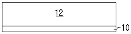
Fig. 1 illustrates a wavelength converting layer disposed on the top surface of an LED.
Fig. 2 illustrates a structure according to an embodiment of the invention, comprising an LED, a wavelength converting layer and a wavelength converting side coating.
Fig. 3, 4 and 5 illustrate prefabricated wavelength converting structures.
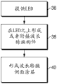
FIG. 6 illustrates a method according to an embodiment of the invention.
Detailed Description
Fig. 1 illustrates a semiconductor device, such as an LED10, having a wavelength converting structure 12, such as a phosphor layer disposed on a top surface of the LED. The wavelength converting structure 12 may be a prefabricated structure, i.e. fabricated separately from the LED10 and then attached to the LED 10. One example of a prefabricated wavelength converting structure 12 is a ceramic phosphor, which is described in more detail in US 7,361,938, which is incorporated herein by reference. The ceramic phosphor may be formed by sintering a powder phosphor into a ceramic body. The phosphor particles are heated until they begin to melt and bond together. The heated phosphor particles are then formed into a ceramic slab. The ceramic slabs may be free of conventional binder materials such as organic binder materials, epoxy, silicone, inorganic binder materials, and glass. Another example of a prefabricated wavelength converting structure 12 is a phosphor or other wavelength converting material arranged in a transparent matrix such as glass or silicone. The prefabricated wavelength converting structure is typically formed as a large sheet, which is then separated into structures having a size corresponding to the size of the LED 10. As a result, the prefabricated wavelength converting structure 12 does not typically cover the sides of the LED10, as shown in fig. 1.
The prefabricated wavelength converting structure 12 is typically thick compared to the thickness of the LED 10. For example, a ceramic phosphor slab or glass member with embedded phosphor may be 200 Thick, while the LED10 may be 50
 Is thick. Due to the thickness of the
 wavelength converting structure 12, some light is emitted from the sides of the wavelength converting structure 12. Side light is undesirable because it can cause a change in the appearance of light emitted from the structure shown in fig. 1, depending on the viewing angle.
In an embodiment of the invention, the wavelength converting material is arranged on the side of the wavelength converted LED. The wavelength converting side coating may reduce color versus angle variations in light emitted from the structure and may improve utilization of light from the LED.
Fig. 2 illustrates a structure according to an embodiment of the present invention. A semiconductor light emitting device such as LED10 is provided. Although in the following examples the semiconductor light emitting device is a group III nitride LED emitting blue or UV light, semiconductor light emitting devices other than LEDs, such as laser diodes, and semiconductor light emitting devices made of other material systems such as other group III-v materials, group III phosphides, group III arsenides, group ii-vi materials, ZnO, or silicon-based materials may be used.
Any suitable group III nitride LED may be used and such LEDs are well known. The LED10 may be, for example, a flip-chip device configured to emit a majority of light from a top surface of the LED. To form such an LED, a group III nitride semiconductor structure is first grown on a growth substrate, as is known in the art. The growth substrate may be any suitable substrate, such as, for example, sapphire, SiC, Si, GaN, or composite substrates. The semiconductor structure includes a light emitting or active region sandwiched between an n-type region and a p-type region. The n-type region may be grown first and may include multiple layers of different compositions and dopant concentrations, including, for example, preparation layers such as buffer layers or nucleation layers, and/or layers designed to facilitate removal of the growth substrate, which may be n-type or unintentionally doped, as well as n-type or even p-type device layers designed for specific optical, material, or electrical properties desired for efficient light emission from the light emitting region. A light emitting or active region is grown over the n-type region. Examples of suitable light emitting regions include a single thick or thin light emitting layer, or a multiple quantum well light emitting region including multiple thin or thick light emitting layers separated by barrier layers. A p-type region may then be grown over the light emitting region. Like the n-type region, the p-type region may include multiple layers of different compositions, thicknesses, and doping concentrations, including layers that are not intentionally doped, or n-type layers. The total thickness of all semiconductor materials in the device is less than 10 in some embodiments And in some embodiments less than 6
 。
。
A metal p-contact is formed on the p-type region. The p-contact may be reflective if a substantial portion of the light is directed away from the semiconductor structure through a surface opposite the p-contact (such as in a flip-chip device). The flip chip device may be formed by patterning the semiconductor structure by standard photolithographic operations and etching the semiconductor structure to remove a portion of the entire thickness of the p-type region and a portion of the entire thickness of the light emitting region to form a mesa that exposes the surface of the n-type region on which the metal n-contact is formed. The mesas and p and n contacts may be formed in any suitable manner. The formation of mesas and p and n contacts is well known to those skilled in the art.
The semiconductor structure may be connected to the support by p and n contacts. A support is a structure that mechanically supports a semiconductor structure. The support is a self-supporting structure adapted to be attached to a structure on which the LED10 is mounted. For example, the support may be reflowable. Any suitable support may be used. Examples of suitable supports include an insulating or semi-insulating wafer (such as a silicon wafer) having conductive vias for making electrical connections to the semiconductor structure, thick metal bond pads formed on the semiconductor structure, for example by plating, or a ceramic, metal or any other suitable mount.
The LED10, including the semiconductor structure, metal contacts and support described above, may optionally be attached to a mount 16. Mount 16 may be optically reflective and thermally conductive. Electrical contact to the LED10 may be made through the mount 16. Examples of suitable mounts 16 include metal core printed circuit boards, FR 4-based printed circuit boards, ceramics, metals, copper, plastics, and silicones. In some embodiments, the top surface of mount 16 is reflective, or coated with a reflective substance such as a reflective paint or a reflective metal layer. The mount 16 may have a thermal conductivity of at least 0.1W/mK (silicone) in some embodiments, at least 10W/mK in some embodiments, and at least 100W/mK in some embodiments, and between 0.1W/mK and 400W/mK in some embodiments.
A wavelength converting layer 12 is formed on the top surface of the LED 10. The wavelength converting layer 12 may be one or more conventional phosphors, organic phosphors, amountsA sub-dot, an organic semiconductor, a group ii-vi or iii-v semiconductor quantum dot or nanocrystal, a dye, a polymer, or a light emitting material such as GaN. Any suitable phosphor may be used, including but not limited to garnet-based phosphors, Y3Al5O12:Ce、Lu3Al5O12:Ce、Y3Al5-xGaxO12:Ce、(Ba1-xSrx)SiO3Eu (BOSE), nitride-based phosphor, and (Ca, Sr) AlSiN3Eu and (Ca, Sr, Ba)2Si5N8Eu. The wavelength converting material 12 may comprise a single wavelength converting material or a plurality of wavelength converting materials that may be mixed together or arranged on top of the LEDs 10 in separate layers. The wavelength converting layer does not typically cover the sides of the LED10, although in some embodiments the wavelength converting layer 12 may extend over the sides of the LED10, and a second wavelength converting layer 22, described below, may be formed over the portion of the wavelength converting layer 12 that covers the sides of the LED 10.
In some embodiments, the wavelength converting layer 12 is formed while it is attached to the LED 10. Examples of such wavelength converting layers include powder phosphors formed by electrophoretic deposition, and dyes or powder phosphors molded, screen printed, sprayed, or infused over the LED10 mixed with a transparent binder material such as silicone or epoxy.
In some embodiments, the wavelength converting layer 12 is a prefabricated wavelength converting layer such as a ceramic phosphor or a wavelength converting material disposed in glass or another transparent solid material. Suitable prefabricated wavelength converting materials are described in the text accompanying fig. 1 above. The prefabricated wavelength converting layer 12 may be attached to the top surface of the LED10 by a transparent bonding layer 20, which transparent bonding layer 20 may be any suitable bonding material, such as epoxy, silicone or glass. Alternatively, the prefabricated wavelength converting layer 12 may be attached to the LED10 without a bonding layer, for example by sintering or hot pressing.
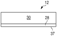
Fig. 3, 4 and 5 illustrate examples of different prefabricated wavelength converting members 12. In the wavelength converting member 12 shown in fig. 3, the wavelength converting material 28 is confined to the portion of the wavelength converting member that is furthest from the LED 10. (the LED10 is disposed proximate the bottom surface 32 of the wavelength converting member 12). The remaining portion 30 of the wavelength converting member 12 may be a transparent material, or a scattering structure. For example, the wavelength converting material 28 may be a phosphor disposed in a transparent material such as glass. The transparent portion 30 may be glass without wavelength converting material with or without scattering particles embedded in the glass. The wavelength converting member 12 may be a ceramic phosphor. Phosphors typically include a crystalline matrix and an activating dopant. For example, the YAG crystal may be doped with the activating dopant cerium and/or europium as is known in the art. Activating the dopant causes the crystalline matrix to emit light. In a ceramic phosphor formed according to the structure shown in fig. 3, portion 28 may include a crystalline matrix and an activating dopant. Portion 30 may include only the crystalline matrix without the activated dopant. The portions 28 and 30 may be sintered together into a ceramic slab, as described above.
In the wavelength converting member 12 shown in fig. 4, the wavelength converting portion 28 is limited to the portion of the wavelength converting member 12 closest to the LED (bottom surface 32). The transparent portion 30 is located above the wavelength converting portion 28.
In the wavelength converting member 12 shown in fig. 5, the wavelength converting portion 28 is arranged at the center of the wavelength converting member 12. The transparent portions 30A and 30B are disposed above and below the wavelength converting portion 28.
Returning to FIG. 2, a side coating 22 is formed on the sides of the LED10 and wavelength-converting layer 12. The side coating 22 may include a wavelength converting material 26 disposed in a transparent matrix 24. The wavelength converting material 26 may be one or more conventional phosphors, organic phosphors, quantum dots, organic semiconductors, ii-vi or iii-v semiconductor quantum dots or nanocrystals, dyes, polymers, or light emitting materials such as GaN. Any suitable phosphor may be used, including but not limited to garnet-based phosphors, Y3Al5O12:Ce、Lu3Al5O12:Ce、Y3Al5-xGaxO12:Ce、(Ba1- xSrx)SiO3Eu (BOSE), nitride-based phosphor, and (Ca, Sr) AlSiN3Eu and (Ca, Sr, Ba)2Si5N8Eu. The wavelength converting material 26 may comprise a single wavelength converting material or a plurality of wavelength converting materials that may be mixed together or arranged on the sides of the structure in separate layers.
In some embodiments, the side coating 22 is configured to scatter light incident thereon. In some embodiments, a scattering wavelength conversion material such as a powdered phosphor is used. In some embodiments, such as TiO2Scattering particles such as or any other suitable scattering material are mixed with the scattering or non-scattering wavelength converting material in the side coating 22. Alternatively, the scattering particles may be formed above or below the wavelength-converting side coating 22 as a separate side coating layer.
The transparent substrate 24 may be any suitable transparent material such as silicone or epoxy. In some embodiments, the transparent matrix 24 is omitted and the wavelength converting material 26 is applied directly to the sides of the LED10 and the wavelength converting member 12.
The side coating 22 may be formed by any suitable technique. In some embodiments, the side coating 22 is formed by mixing a wavelength converting material, such as a powdered phosphor, with a liquid matrix material, such as silicone, to form a slurry. The slurry may be formed into a sheet that is then partially cured so that the sheet is flexible. The flexible sheet is then laminated to the sides of the LED10 using a commercially available laminator. Alternatively, the slurry may be dispensed on the sides of the LED10, for example, by using a syringe, and then cured to a solid at an elevated temperature, for example, 150 ℃. Alternatively, the slurry may be applied to the sides of the LED10 using a doctor blade and then cured to a solid at an elevated temperature, such as 150 ℃. In some embodiments, a side coating 22 is molded over the LED 10. A mold of appropriate size and shape is positioned over the LED10 and then filled with a wavelength converting material mixed with a liquid matrix material. The liquid matrix material is cured to a solid and the mold is then removed, leaving the side coating 22. In some embodiments, the wavelength converting material is disposed over the top and sides of the LED10, and then the wavelength converting material is removed from the top of the LED10, for example by scraping, leaving only the side coating 22.
In some embodiments, the side coating 22 is formed to be sufficiently thick such that all or most of the light incident on the side coating is wavelength converted. In some embodiments, the thickness of the side coating 22 is selected to allow some unconverted light from the LED to escape.
In some embodiments, the side coating 22 is configured to create a uniform color distribution independent of viewing angle.
As described above, each of the wavelength converting regions 12 and 22 may include a single wavelength converting material or a plurality of wavelength converting materials that are mixed or separated. In some embodiments, the wavelength converting regions 12 and 22 comprise different wavelength converting materials. In some embodiments, a red emitting phosphor is disposed on the side of the LED10 and a green or yellow emitting phosphor is disposed on top of the LED 10. In some embodiments, a mixture of red-emitting and green/yellow-emitting phosphors is disposed on both the top and sides of the LED. In some embodiments, a mixture of red-emitting phosphors and red-emitting quantum dots is disposed on the sides of the LED10, and a mixture of multiple types of green-emitting phosphors is disposed on the top of the LED 10. In some embodiments, a single red light emitting phosphor is disposed on the side of the LED10, and a mixture of the same or different red and green/yellow light emitting phosphors is disposed on top of the LED 10. The embodiments described above are only a few of the many possible combinations that can be envisaged by a person skilled in the art and are within the scope of the invention.
In some embodiments, the device comprises a wavelength converting material a that can be excited by light emitted by another wavelength converting material B. The wavelength converting material a may be disposed on the sides of the LED10, while the wavelength converting material B may be disposed on the top of the LED10 to minimize interaction between the wavelength converting materials.
For example, devices that produce white light typically include a blue LED and a red and green or yellow light emitting phosphor. Many phosphors that emit red light will absorb the light emitted by a green or yellow emitting phosphor. In some embodiments, the red emitting phosphor is disposed on the sides of the LED10 and the green or yellow emitting phosphor is disposed on top of the LED 10. In such an arrangement, the red-emitting phosphor may absorb less green or yellow light than in a system in which red and green/yellow phosphors are mixed, which may improve the color rendering index of the mixed light, may improve the efficiency of the device, and may simplify color targeting.
Fig. 6 illustrates a method of forming the structure shown in fig. 2. In stage 36, the LED10 is provided. The LED10 may be attached to the mount 16, although it need not be. In stage 38, the wavelength converting member 12 is attached to the LED10, or formed over the LED10, in the case of a prefabricated wavelength converting member. In stage 40, a wavelength converting side coating 22 is formed over the LED 10. The wavelength converting side coating 22 typically covers the sides of both the LED10 and the wavelength converting member 12, although in some embodiments the wavelength converting side coating 22 may cover only the sides of the LED10 or only the wavelength converting member 12, or a portion of the sides of one or both of the LED10 and the wavelength converting member 12.
Embodiments of the invention may provide several advantages. When the scattering from the wavelength converting layer on top of the LED increases, the light efficiency of the wavelength converted LED decreases. In some embodiments, some of the scattering wavelength converting material is removed from the top of the LED and placed on the sides, which may improve the efficiency of the structure. Applying a wavelength converting material to the side faces of the LED may provide another parameter that can be tuned to reach the desired color point of the light emitted by the structure, which may simplify color targeting or improve the efficiency of the structure. The use of a wavelength converting side coating may reduce or eliminate the need to use scattering particles in the structure, which may reduce cost and/or complexity of the structure. The use of a wavelength converting side coating may reduce the variation of color with respect to angle in the light emitted by the structure. The use of wavelength converting side coatings may permit wavelength converting materials to separate, which may improve efficiency by reducing interactions between wavelength converting regions.
Having described the invention in detail, those skilled in the art will appreciate that, in view of the present disclosure, modifications may be made to the invention without departing from the spirit of the inventive concepts described herein. Therefore, it is not intended that the scope of the invention be limited to the specific embodiments illustrated and described.
Claims (15)
1. A semiconductor structure, comprising:
a semiconductor light emitting device;
a first wavelength converting member disposed on a first surface of the semiconductor light emitting device, wherein the first wavelength converting member is no wider than the first surface; and
a second wavelength converting member on a side surface of the semiconductor light emitting device, wherein the second wavelength converting member does not extend over the first surface;
wherein the first wavelength converting member comprises a first wavelength converting material in direct contact with the first surface, the second wavelength converting member is different from the first wavelength converting material, and the second wavelength converting material is excitable by light emitted by the first wavelength converting material.
2. The semiconductor structure of claim 1, wherein the first wavelength converting member comprises a prefabricated wavelength converting member.
3. The semiconductor structure of claim 2, wherein the first wavelength converting member comprises a phosphor embedded in a transparent material.
4. The semiconductor structure of claim 1, wherein the first wavelength converting member comprises a ceramic phosphor.
5. The semiconductor structure of claim 1, wherein the second wavelength converting member comprises a powder phosphor disposed in a transparent matrix.
6. The semiconductor structure of claim 1, wherein:
the first wavelength converting member includes a wavelength converting material that emits green or yellow light; and is
The second wavelength converting member comprises a wavelength converting material that emits red light.
7. The semiconductor structure of claim 1, wherein the second wavelength converting member comprises scattering particles.
8. A method for fabricating a semiconductor structure, comprising:
providing a semiconductor light emitting device;
disposing a first wavelength converting material over a first surface of the semiconductor light emitting device, wherein the first wavelength converting material is confined to an area no wider than the first surface and directly contacts the first surface; and
after disposing the first wavelength converting material over the first surface of the semiconductor light emitting device, laminating a second wavelength converting material over the side surfaces of the semiconductor light emitting device, wherein the sheet of second wavelength converting material does not extend over the first surface, and
wherein the second wavelength converting material is excitable by light emitted by the first wavelength converting material.
9. The method for fabricating the semiconductor structure as recited in claim 8, wherein disposing the first wavelength converting material over the first surface of the semiconductor light emitting device comprises attaching a prefabricated wavelength converting member to the first surface of the semiconductor light emitting device.
10. The method for fabricating a semiconductor structure as recited in claim 9, wherein the first wavelength converting material is a ceramic phosphor.
11. The method for fabricating a semiconductor structure according to claim 9, wherein the first wavelength converting material is a phosphor embedded in glass.
12. The method for fabricating a semiconductor structure according to claim 9, wherein the prefabricated wavelength converting member comprises a first region of wavelength converting material and a second region of transparent material.
13. The method for fabricating the semiconductor structure as recited in claim 12, wherein attaching the prefabricated wavelength converting member to the first surface of the semiconductor light emitting device comprises attaching the prefabricated wavelength converting member such that the first region is disposed between the semiconductor light emitting device and the second region.
14. The method for fabricating the semiconductor structure as recited in claim 12, wherein attaching the prefabricated wavelength converting member to the first surface of the semiconductor light emitting device comprises attaching the prefabricated wavelength converting member such that the second region is disposed between the semiconductor light emitting device and the first region.
15. The method for fabricating a semiconductor structure as claimed in claim 8, wherein the first and second wavelength converting materials emit different colors of light.
Applications Claiming Priority (3)
| Application Number | Priority Date | Filing Date | Title |
|---|---|---|---|
| US201261617903P | 2012-03-30 | 2012-03-30 | |
| US61/617903 | 2012-03-30 | ||
| PCT/IB2013/052390 WO2013144834A1 (en) | 2012-03-30 | 2013-03-26 | Light emitting device with wavelength converting side coat |
Publications (2)
| Publication Number | Publication Date |
|---|---|
| CN104205374A CN104205374A (en) | 2014-12-10 |
| CN104205374B true CN104205374B (en) | 2020-10-16 |
Family
ID=48326370
Family Applications (1)
| Application Number | Title | Priority Date | Filing Date |
|---|---|---|---|
| CN201380018279.XA Active CN104205374B (en) | 2012-03-30 | 2013-03-26 | Light emitting device with wavelength converting side coating |
Country Status (7)
| Country | Link |
|---|---|
| US (2) | US10043952B2 (en) |
| EP (1) | EP2831932B1 (en) |
| JP (1) | JP6435258B2 (en) |
| KR (1) | KR20150004818A (en) |
| CN (1) | CN104205374B (en) |
| RU (1) | RU2639565C2 (en) |
| WO (1) | WO2013144834A1 (en) |
Families Citing this family (14)
| Publication number | Priority date | Publication date | Assignee | Title |
|---|---|---|---|---|
| JP2015176960A (en) * | 2014-03-14 | 2015-10-05 | 株式会社東芝 | light-emitting device |
| CN104953014B (en) * | 2014-03-28 | 2019-01-29 | 深圳光峰科技股份有限公司 | A kind of multilayered structure glass phosphor sheet and preparation method thereof and light emitting device |
| KR20150116986A (en) * | 2014-04-08 | 2015-10-19 | 삼성디스플레이 주식회사 | Quantum dot sheet and light unit and liquid crystal display including the same |
| KR102408839B1 (en) * | 2014-06-19 | 2022-06-14 | 루미리즈 홀딩 비.브이. | Wavelength converted light emitting device with small source size |
| US9373761B2 (en) * | 2014-09-23 | 2016-06-21 | Osram Sylvania Inc. | Patterned thin-film wavelength converter and method of making same |
| JP6484982B2 (en) | 2014-09-30 | 2019-03-20 | 日亜化学工業株式会社 | Method for manufacturing light emitting device |
| CN104465540A (en) * | 2014-12-22 | 2015-03-25 | 永新电子常熟有限公司 | Electronic chip with good stability |
| KR20170026801A (en) * | 2015-08-28 | 2017-03-09 | 삼성전자주식회사 | Semiconductor light emitting device package and light source module using the same |
| CN107068841A (en) * | 2017-04-11 | 2017-08-18 | 安徽芯瑞达科技股份有限公司 | Luminous quantum dot interlayer CSP backlights in a kind of five face and preparation method thereof |
| CN111213249B (en) * | 2017-08-18 | 2023-10-03 | 奥斯兰姆奥普托半导体有限责任公司 | Production of semiconductor devices |
| TWI658610B (en) * | 2017-09-08 | 2019-05-01 | Maven Optronics Co., Ltd. | Quantum-dot-based color-converted light emitting device and method for manufacturing the same |
| KR102593592B1 (en) * | 2018-05-04 | 2023-10-25 | 엘지이노텍 주식회사 | Lighting apparatus |
| JP7057508B2 (en) * | 2019-03-28 | 2022-04-20 | 日亜化学工業株式会社 | Light emitting device |
| JP7283327B2 (en) | 2019-09-20 | 2023-05-30 | セイコーエプソン株式会社 | Wavelength conversion element, light source device and projector |
Citations (4)
| Publication number | Priority date | Publication date | Assignee | Title |
|---|---|---|---|---|
| CN101657910A (en) * | 2006-11-20 | 2010-02-24 | 皇家飞利浦电子股份有限公司 | Light emitting device including luminescent ceramic and light-scattering material |
| CN101673787A (en) * | 2008-09-12 | 2010-03-17 | 晶元光电股份有限公司 | Semiconductor luminous device and packaging structure thereof |
| CN102208521A (en) * | 2004-06-03 | 2011-10-05 | 皇家飞利浦电子股份有限公司 | Luminescent ceramic for a light emitting device |
| WO2012025377A1 (en) * | 2010-08-26 | 2012-03-01 | Osram Opto Semiconductors Gmbh | Radiation-emitting component and method for producing a radiation-emitting component |
Family Cites Families (40)
| Publication number | Priority date | Publication date | Assignee | Title |
|---|---|---|---|---|
| US5959316A (en) | 1998-09-01 | 1999-09-28 | Hewlett-Packard Company | Multiple encapsulation of phosphor-LED devices |
| US6351069B1 (en) | 1999-02-18 | 2002-02-26 | Lumileds Lighting, U.S., Llc | Red-deficiency-compensating phosphor LED |
| US6680569B2 (en) | 1999-02-18 | 2004-01-20 | Lumileds Lighting U.S. Llc | Red-deficiency compensating phosphor light emitting device |
| TW455908B (en) | 1999-04-20 | 2001-09-21 | Koninkl Philips Electronics Nv | Lighting system |
| US6504301B1 (en) | 1999-09-03 | 2003-01-07 | Lumileds Lighting, U.S., Llc | Non-incandescent lightbulb package using light emitting diodes |
| AT410266B (en) | 2000-12-28 | 2003-03-25 | Tridonic Optoelectronics Gmbh | LIGHT SOURCE WITH A LIGHT-EMITTING ELEMENT |
| JP4081985B2 (en) | 2001-03-02 | 2008-04-30 | 日亜化学工業株式会社 | Light emitting device and manufacturing method thereof |
| ATE525755T1 (en) * | 2001-10-12 | 2011-10-15 | Nichia Corp | LIGHT-EMITTING COMPONENT AND METHOD FOR THE PRODUCTION THEREOF |
| US6791116B2 (en) * | 2002-04-30 | 2004-09-14 | Toyoda Gosei Co., Ltd. | Light emitting diode |
| KR101030068B1 (en) * | 2002-07-08 | 2011-04-19 | 니치아 카가쿠 고교 가부시키가이샤 | Method of Manufacturing Nitride Semiconductor Device and Nitride Semiconductor Device |
| JP4337574B2 (en) * | 2003-09-25 | 2009-09-30 | 日亜化学工業株式会社 | LIGHT EMITTING DEVICE AND METHOD FOR FORMING THE SAME |
| US7052152B2 (en) | 2003-10-03 | 2006-05-30 | Philips Lumileds Lighting Company, Llc | LCD backlight using two-dimensional array LEDs |
| US7102152B2 (en) * | 2004-10-14 | 2006-09-05 | Avago Technologies Ecbu Ip (Singapore) Pte. Ltd. | Device and method for emitting output light using quantum dots and non-quantum fluorescent material |
| US7250715B2 (en) | 2004-02-23 | 2007-07-31 | Philips Lumileds Lighting Company, Llc | Wavelength converted semiconductor light emitting devices |
| JP4756841B2 (en) * | 2004-09-29 | 2011-08-24 | スタンレー電気株式会社 | Manufacturing method of semiconductor light emitting device |
| US7858408B2 (en) | 2004-11-15 | 2010-12-28 | Koninklijke Philips Electronics N.V. | LED with phosphor tile and overmolded phosphor in lens |
| JP4845370B2 (en) * | 2004-11-26 | 2011-12-28 | 京セラ株式会社 | Light emitting device and lighting device |
| JP2006352036A (en) * | 2005-06-20 | 2006-12-28 | Rohm Co Ltd | White semiconductor light-emitting device |
| RU2303833C2 (en) | 2005-07-26 | 2007-07-27 | Самсунг Электро-Меканикс Ко., Лтд. | Lighting unit |
| WO2007052777A1 (en) | 2005-11-04 | 2007-05-10 | Matsushita Electric Industrial Co., Ltd. | Light-emitting module, and display unit and lighting unit using the same |
| KR101019765B1 (en) | 2006-01-04 | 2011-03-04 | 로무 가부시키가이샤 | Thin-type light emitting diode lamp, and its manufacturing |
| US8232564B2 (en) * | 2007-01-22 | 2012-07-31 | Cree, Inc. | Wafer level phosphor coating technique for warm light emitting diodes |
| JP4920497B2 (en) | 2007-05-29 | 2012-04-18 | 株式会社東芝 | Optical semiconductor device |
| US7942556B2 (en) | 2007-06-18 | 2011-05-17 | Xicato, Inc. | Solid state illumination device |
| CN101809768B (en) * | 2007-08-31 | 2012-04-25 | Lg伊诺特有限公司 | Light emitting device package |
| US7984999B2 (en) | 2007-10-17 | 2011-07-26 | Xicato, Inc. | Illumination device with light emitting diodes and moveable light adjustment member |
| ES2397208T3 (en) | 2008-08-08 | 2013-03-05 | Xicato, Inc. | Adjustable color light source |
| JP5284006B2 (en) * | 2008-08-25 | 2013-09-11 | シチズン電子株式会社 | Light emitting device |
| US7973327B2 (en) * | 2008-09-02 | 2011-07-05 | Bridgelux, Inc. | Phosphor-converted LED |
| CN102165611B (en) | 2008-09-25 | 2014-04-23 | 皇家飞利浦电子股份有限公司 | Coated light emitting device and method for coating thereof |
| US7804103B1 (en) * | 2009-01-07 | 2010-09-28 | Lednovation, Inc. | White lighting device having short wavelength semiconductor die and trichromatic wavelength conversion layers |
| KR101172143B1 (en) * | 2009-08-10 | 2012-08-07 | 엘지이노텍 주식회사 | OXYNITRIDE-BASED PHOSPHORS COMPOSING OF SiON ELEMENT FOR WHITE LEDs, MANUFACTURING METHOD THEREOF AND LEDs USING THE SAME |
| KR101163902B1 (en) | 2010-08-10 | 2012-07-09 | 엘지이노텍 주식회사 | Light emitting device |
| US8104908B2 (en) | 2010-03-04 | 2012-01-31 | Xicato, Inc. | Efficient LED-based illumination module with high color rendering index |
| KR20130063496A (en) | 2010-04-26 | 2013-06-14 | 시카토, 인코포레이티드. | Led-based illumination module attachment to a light fixture |
| DE102010021011A1 (en) | 2010-05-21 | 2011-11-24 | Osram Opto Semiconductors Gmbh | Optoelectronic semiconductor component and method for producing a cover layer |
| US20110317397A1 (en) | 2010-06-23 | 2011-12-29 | Soraa, Inc. | Quantum dot wavelength conversion for hermetically sealed optical devices |
| DE102010053362B4 (en) | 2010-12-03 | 2021-09-30 | OSRAM Opto Semiconductors Gesellschaft mit beschränkter Haftung | Method for producing a radiation-emitting semiconductor chip, radiation-emitting semiconductor chip and radiation-emitting component |
| JP5895598B2 (en) | 2012-02-29 | 2016-03-30 | 日亜化学工業株式会社 | Light emitting device |
| US9071981B2 (en) | 2012-09-21 | 2015-06-30 | Htc Corporation | Method of monitoring search space of enhanced downlink control channel in orthogonal frequency-division multiple access system |
-
2013
- 2013-03-26 KR KR1020147030414A patent/KR20150004818A/en not_active IP Right Cessation
- 2013-03-26 US US14/388,979 patent/US10043952B2/en active Active
- 2013-03-26 WO PCT/IB2013/052390 patent/WO2013144834A1/en active Application Filing
- 2013-03-26 RU RU2014143771A patent/RU2639565C2/en active IP Right Revival
- 2013-03-26 CN CN201380018279.XA patent/CN104205374B/en active Active
- 2013-03-26 JP JP2015502519A patent/JP6435258B2/en active Active
- 2013-03-26 EP EP13721410.2A patent/EP2831932B1/en active Active
-
2017
- 2017-08-23 US US15/684,477 patent/US10224466B2/en active Active
Patent Citations (4)
| Publication number | Priority date | Publication date | Assignee | Title |
|---|---|---|---|---|
| CN102208521A (en) * | 2004-06-03 | 2011-10-05 | 皇家飞利浦电子股份有限公司 | Luminescent ceramic for a light emitting device |
| CN101657910A (en) * | 2006-11-20 | 2010-02-24 | 皇家飞利浦电子股份有限公司 | Light emitting device including luminescent ceramic and light-scattering material |
| CN101673787A (en) * | 2008-09-12 | 2010-03-17 | 晶元光电股份有限公司 | Semiconductor luminous device and packaging structure thereof |
| WO2012025377A1 (en) * | 2010-08-26 | 2012-03-01 | Osram Opto Semiconductors Gmbh | Radiation-emitting component and method for producing a radiation-emitting component |
Also Published As
| Publication number | Publication date |
|---|---|
| EP2831932B1 (en) | 2020-09-30 |
| WO2013144834A1 (en) | 2013-10-03 |
| JP2015511773A (en) | 2015-04-20 |
| JP6435258B2 (en) | 2018-12-05 |
| US10043952B2 (en) | 2018-08-07 |
| US20170352788A1 (en) | 2017-12-07 |
| EP2831932A1 (en) | 2015-02-04 |
| KR20150004818A (en) | 2015-01-13 |
| US20150060917A1 (en) | 2015-03-05 |
| CN104205374A (en) | 2014-12-10 |
| RU2014143771A (en) | 2016-05-27 |
| US10224466B2 (en) | 2019-03-05 |
| RU2639565C2 (en) | 2017-12-21 |
Similar Documents
| Publication | Publication Date | Title |
|---|---|---|
| US10224466B2 (en) | Light emitting device with wavelength converting side coat | |
| JP6595055B2 (en) | Optical resonator including light emitting device and wavelength conversion material | |
| US7810956B2 (en) | Light source including reflective wavelength-converting layer | |
| EP3020076B1 (en) | Wavelength converted semiconductor light emitting device | |
| EP2504870B1 (en) | Wavelength converted semiconductor light emitting diode | |
| US8154052B2 (en) | Light emitting device grown on wavelength converting substrate | |
| KR102237304B1 (en) | Light emitting device with an optical element and a reflector | |
| EP3161880B1 (en) | Packaged wavelength converted light emitting device | |
| US9876149B2 (en) | Semiconductor light emitting device package and light source module using same | |
| US20160204314A1 (en) | Light emitting diode package | |
| WO2013144798A1 (en) | Optical cavity including a light emitting device and wavelength converting material | |
| KR20120128671A (en) | Method of forming a wavelength converting layer for a light emitting diode |
Legal Events
| Date | Code | Title | Description |
|---|---|---|---|
| C06 | Publication | ||
| PB01 | Publication | ||
| C10 | Entry into substantive examination | ||
| SE01 | Entry into force of request for substantive examination | ||
| TA01 | Transfer of patent application right |
Effective date of registration: 20180326 Address after: Holland Schiphol Applicant after: LUMILEDS HOLDING B.V. Address before: Holland Ian Deho Finn Applicant before: Koninkl Philips Electronics NV |
|
| TA01 | Transfer of patent application right | ||
| GR01 | Patent grant | ||
| GR01 | Patent grant |