JP4266350B2 - テスト回路 - Google Patents
テスト回路 Download PDFInfo
- Publication number
- JP4266350B2 JP4266350B2 JP2004034549A JP2004034549A JP4266350B2 JP 4266350 B2 JP4266350 B2 JP 4266350B2 JP 2004034549 A JP2004034549 A JP 2004034549A JP 2004034549 A JP2004034549 A JP 2004034549A JP 4266350 B2 JP4266350 B2 JP 4266350B2
- Authority
- JP
- Japan
- Prior art keywords
- signal
- circuit
- analog
- output
- test circuit
- Prior art date
- Legal status (The legal status is an assumption and is not a legal conclusion. Google has not performed a legal analysis and makes no representation as to the accuracy of the status listed.)
- Expired - Fee Related
Links
- 238000012360 testing method Methods 0.000 title claims description 73
- 230000004044 response Effects 0.000 claims description 32
- 230000010355 oscillation Effects 0.000 claims description 10
- 230000001934 delay Effects 0.000 claims description 2
- 238000012545 processing Methods 0.000 claims description 2
- 238000006243 chemical reaction Methods 0.000 description 69
- 102100020786 Adenylosuccinate synthetase isozyme 2 Human genes 0.000 description 33
- 108091022873 acetoacetate decarboxylase Proteins 0.000 description 28
- 230000000630 rising effect Effects 0.000 description 24
- 101710096655 Probable acetoacetate decarboxylase 1 Proteins 0.000 description 15
- 101000851696 Homo sapiens Steroid hormone receptor ERR2 Proteins 0.000 description 13
- 102100036831 Steroid hormone receptor ERR2 Human genes 0.000 description 13
- 238000010586 diagram Methods 0.000 description 9
- 238000005259 measurement Methods 0.000 description 7
- 230000006870 function Effects 0.000 description 6
- 230000002779 inactivation Effects 0.000 description 6
- 108010032363 ERRalpha estrogen-related receptor Proteins 0.000 description 5
- 102100036832 Steroid hormone receptor ERR1 Human genes 0.000 description 5
- 101150002173 adss1 gene Proteins 0.000 description 5
- 238000012986 modification Methods 0.000 description 5
- 230000004048 modification Effects 0.000 description 5
- 230000004913 activation Effects 0.000 description 4
- 230000000694 effects Effects 0.000 description 4
- 230000001360 synchronised effect Effects 0.000 description 3
- 108010076504 Protein Sorting Signals Proteins 0.000 description 2
- 238000011156 evaluation Methods 0.000 description 2
- 239000004065 semiconductor Substances 0.000 description 2
- 101710096660 Probable acetoacetate decarboxylase 2 Proteins 0.000 description 1
- BNPSSFBOAGDEEL-UHFFFAOYSA-N albuterol sulfate Chemical compound OS(O)(=O)=O.CC(C)(C)NCC(O)C1=CC=C(O)C(CO)=C1.CC(C)(C)NCC(O)C1=CC=C(O)C(CO)=C1 BNPSSFBOAGDEEL-UHFFFAOYSA-N 0.000 description 1
- 230000000737 periodic effect Effects 0.000 description 1
- 230000009467 reduction Effects 0.000 description 1
- 230000003252 repetitive effect Effects 0.000 description 1
- 230000011218 segmentation Effects 0.000 description 1
- 238000010998 test method Methods 0.000 description 1
- 230000001052 transient effect Effects 0.000 description 1
Images


Classifications
-
- G—PHYSICS
- G01—MEASURING; TESTING
- G01R—MEASURING ELECTRIC VARIABLES; MEASURING MAGNETIC VARIABLES
- G01R31/00—Arrangements for testing electric properties; Arrangements for locating electric faults; Arrangements for electrical testing characterised by what is being tested not provided for elsewhere
- G01R31/28—Testing of electronic circuits, e.g. by signal tracer
- G01R31/317—Testing of digital circuits
- G01R31/3181—Functional testing
- G01R31/319—Tester hardware, i.e. output processing circuits
- G01R31/31917—Stimuli generation or application of test patterns to the device under test [DUT]
- G01R31/31924—Voltage or current aspects, e.g. driver, receiver
-
- G—PHYSICS
- G01—MEASURING; TESTING
- G01R—MEASURING ELECTRIC VARIABLES; MEASURING MAGNETIC VARIABLES
- G01R19/00—Arrangements for measuring currents or voltages or for indicating presence or sign thereof
- G01R19/25—Arrangements for measuring currents or voltages or for indicating presence or sign thereof using digital measurement techniques
- G01R19/257—Arrangements for measuring currents or voltages or for indicating presence or sign thereof using digital measurement techniques using analogue/digital converters of the type with comparison of different reference values with the value of voltage or current, e.g. using step-by-step method
-
- G—PHYSICS
- G01—MEASURING; TESTING
- G01R—MEASURING ELECTRIC VARIABLES; MEASURING MAGNETIC VARIABLES
- G01R29/00—Arrangements for measuring or indicating electric quantities not covered by groups G01R19/00 - G01R27/00
- G01R29/02—Measuring characteristics of individual pulses, e.g. deviation from pulse flatness, rise time or duration
- G01R29/027—Indicating that a pulse characteristic is either above or below a predetermined value or within or beyond a predetermined range of values
- G01R29/0276—Indicating that a pulse characteristic is either above or below a predetermined value or within or beyond a predetermined range of values the pulse characteristic being rise time
Landscapes
- Physics & Mathematics (AREA)
- General Physics & Mathematics (AREA)
- Engineering & Computer Science (AREA)
- General Engineering & Computer Science (AREA)
- Tests Of Electronic Circuits (AREA)
- Analogue/Digital Conversion (AREA)
Description
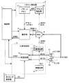
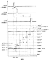
図1は、この発明の実施の形態1によるテスト回路の概略構成を示すブロック図である。図1において、このテスト回路は、ウィンドウコンパレータ1、タイミング発生器2、比較判定部3、解析部6、AD変換器(以下、ADCと称する)4、パターン発生部5および制御部7を備える。
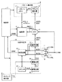
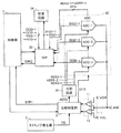
図4は、この発明の実施の形態2によるテスト回路の概略構成を示すブロック図であって、図1と対比される図である。図4のテスト回路を参照して、図1のテスト回路と異なる点は、比較判定部3が比較判定部21で置換されている点である。比較判定部3の発振回路14は、比較判定部21においてカウンタ22、記憶回路23および遅延回路24で置換されている。なお、図4において、図1と対応する部分においては同一符号を付し、その詳細説明を省略する。
図8は、この発明の実施の形態3によるテスト回路の概略構成を示すブロック図であって、図1と対比される図である。図8のテスト回路を参照して、図1のテスト回路と異なる点は、分割回路31が追加され、ADC4がADC32で置換され、解析部6がDSP(Digital Signal Processor)33で置換され、パターン発生部5が記憶回路34で置換されている点である。なお、図8において、図1と対応する部分においては同一符号を付し、その詳細説明を省略する。
図10は、この発明の実施の形態3の変更例によるテスト回路の概略構成を示すブロック図であって、図8と対比される図である。図10のテスト回路を参照して、図8のテスト回路と異なる点は、分割回路31が削除され、ADC32がADC41で置換されている点である。なお、図10において、図8と対応する部分においては同一符号を付し、その詳細説明を省略する。
Claims (9)
- デバイスのアナログ信号の特性を評価するテスト回路であって、
前記デバイスのアナログ信号の電位が予め定められた範囲内にある場合は第1の信号を出力し、前記デバイスのアナログ信号の電位が予め定められた範囲内にはない場合は第2の信号を出力するコンパレータ、
パルス信号列であるタイミング信号を生成するタイミング発生器、
前記タイミング信号に同期して動作し、前記コンパレータの出力信号と予め定められた期待値データとが一致するかどうかを判定する判定回路、
クロック信号を生成するクロック発生回路、
前記コンパレータの出力信号を受け、前記第1の信号に応答して前記クロック発生回路からのクロック信号を通過させて出力し、前記第2の信号に応答して前記クロック発生回路からのクロック信号を遮断する論理回路、
前記論理回路の出力信号に同期して動作し、前記デバイスのアナログ信号をデジタルデータに変換して出力するアナログデジタル変換器、および
前記アナログデジタル変換器からのデジタルデータを解析する解析部を備え、
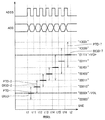
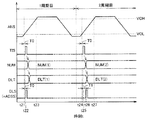
前記判定回路は、前記アナログ信号の波形の傾斜部分のタイミングが予め定められた範囲内にあるかどうかを判定するファンクションテストを行ない、
前記解析部は、前記アナログ信号の波形の傾斜状態を評価する傾斜波形テストを行なう、テスト回路。 - 前記解析部は、
前記アナログデジタル変換器から前記解析部に出力されるデジタルデータに対応した期待値パターンデータを生成するパターン発生部、および
前記デジタルデータが前記期待値パターンデータによって定められる範囲内にあるかどうかを判定する副解析部を含む、請求項1に記載のテスト回路。 - 前記クロック発生回路は、所定周期のパルス信号列である前記クロック信号を生成する発振回路を含む、請求項1または請求項2に記載のテスト回路。
- 前記クロック発生回路は、
前記タイミング発生器からのタイミング信号のパルス数をカウントして出力するカウンタ、および
前記カウンタによってカウントされたパルス数に応じて遅延時間を定め、定められた遅延時間だけ前記タイミング信号を遅延させた信号を前記クロック信号として出力する遅延回路を含む、請求項1または請求項2に記載のテスト回路。 - 前記パターン発生部は、前記デジタルデータおよび前記期待値パターンデータを記憶する記憶回路を含み、
前記副解析部は、前記記憶回路のデータの書込みおよび読出しを行なう演算処理部を含む、請求項2から請求項4までのいずれかに記載のテスト回路。 - さらに、前記論理回路からのクロック信号をそれぞれ位相の異なる複数のクロック信号に分割して出力する分割回路を備え、
前記アナログデジタル変換器は、それぞれ前記複数のクロック信号に対応して設けられ、それぞれ対応する前記複数のクロック信号に同期して動作し、前記デバイスのアナログ信号をデジタルデータに変換して出力する複数のアナログデジタル変換回路を含む、請求項1から請求項5までのいずれかに記載のテスト回路。 - 前記アナログデジタル変換器は、
それぞれ異なったオフセット電源電圧を有する複数のオフセット電源、および
それぞれ前記複数のオフセット電源に対応して設けられ、それぞれ対応する前記複数のオフセット電源のオフセット電源電圧によって定められる電圧レンジにおいて、前記デバイスのアナログ信号をデジタルデータに変換して出力する複数のアナログデジタル変換回路を含む、請求項1から請求項5までのいずれかに記載のテスト回路。 - 前記テスト回路は、前記デバイスのチップに内蔵される、請求項1から請求項7までのいずれかに記載のテスト回路。
- 前記テスト回路は、前記デバイスの外部のテスタに設けられる、請求項1から請求項7までのいずれかに記載のテスト回路。
Priority Applications (2)
| Application Number | Priority Date | Filing Date | Title |
|---|---|---|---|
| JP2004034549A JP4266350B2 (ja) | 2004-02-12 | 2004-02-12 | テスト回路 |
| US11/048,723 US7079060B2 (en) | 2004-02-12 | 2005-02-03 | Test circuit for evaluating characteristic of analog signal of device |
Applications Claiming Priority (1)
| Application Number | Priority Date | Filing Date | Title |
|---|---|---|---|
| JP2004034549A JP4266350B2 (ja) | 2004-02-12 | 2004-02-12 | テスト回路 |
Publications (3)
| Publication Number | Publication Date |
|---|---|
| JP2005227057A JP2005227057A (ja) | 2005-08-25 |
| JP2005227057A5 JP2005227057A5 (ja) | 2006-09-28 |
| JP4266350B2 true JP4266350B2 (ja) | 2009-05-20 |
Family
ID=34836180
Family Applications (1)
| Application Number | Title | Priority Date | Filing Date |
|---|---|---|---|
| JP2004034549A Expired - Fee Related JP4266350B2 (ja) | 2004-02-12 | 2004-02-12 | テスト回路 |
Country Status (2)
| Country | Link |
|---|---|
| US (1) | US7079060B2 (ja) |
| JP (1) | JP4266350B2 (ja) |
Families Citing this family (13)
| Publication number | Priority date | Publication date | Assignee | Title |
|---|---|---|---|---|
| US7856330B2 (en) * | 2006-02-27 | 2010-12-21 | Advantest Corporation | Measuring apparatus, testing apparatus, and electronic device |
| US7554332B2 (en) * | 2006-03-10 | 2009-06-30 | Advantest Corporation | Calibration apparatus, calibration method, testing apparatus, and testing method |
| US7525349B2 (en) * | 2006-08-14 | 2009-04-28 | University Of Washington | Circuit for classifying signals |
| US8738331B2 (en) * | 2007-06-07 | 2014-05-27 | Abb Technology Ag | Increased reliability in the processing of digital signals |
| JP2010103737A (ja) * | 2008-10-23 | 2010-05-06 | Toshiba Corp | Adcテスト回路 |
| US8624764B2 (en) * | 2011-02-11 | 2014-01-07 | Analog Devices, Inc. | Test circuits and methods for redundant electronic systems |
| TWI483555B (zh) * | 2011-12-15 | 2015-05-01 | Silicon Motion Inc | 測試裝置以及類比至數位轉換器之測試方法 |
| DE102013209309A1 (de) * | 2013-05-21 | 2014-11-27 | Zf Friedrichshafen Ag | Verfahren und Schaltung zur Bewertung pulsweitenmodulierter Signale |
| DE102015116786A1 (de) * | 2015-10-02 | 2017-04-06 | Infineon Technologies Ag | Vorrichtungsverfahren zum Testen eines Analog-Digital Wandlers |
| US11055255B2 (en) * | 2019-04-25 | 2021-07-06 | Realtek Semiconductor Corporation | Interface connection apparatus and method |
| CN111858438B (zh) * | 2019-04-30 | 2022-03-01 | 瑞昱半导体股份有限公司 | 接口连接装置与方法 |
| TWI785952B (zh) * | 2021-12-30 | 2022-12-01 | 新唐科技股份有限公司 | 密碼加速器以及加解密運算的差分故障分析方法 |
| TWI827237B (zh) * | 2022-09-06 | 2023-12-21 | 新唐科技股份有限公司 | 密碼加速器以及加解密運算防篡改方法 |
Family Cites Families (7)
| Publication number | Priority date | Publication date | Assignee | Title |
|---|---|---|---|---|
| US4908621A (en) * | 1988-07-06 | 1990-03-13 | Tektronix, Inc. | Autocalibrated multistage A/D converter |
| JP3144563B2 (ja) | 1991-02-18 | 2001-03-12 | 横河電機株式会社 | 波形測定装置 |
| JPH0514200A (ja) | 1991-06-28 | 1993-01-22 | Fuji Facom Corp | 高精度化adコンバータ |
| US5352976A (en) * | 1992-01-31 | 1994-10-04 | Tektronix, Inc. | Multi-channel trigger dejitter |
| TW364950B (en) * | 1996-06-17 | 1999-07-21 | Koninkl Philips Electronics Nv | Method of testing an analog-to-digital converter |
| JP2000292469A (ja) | 1999-04-09 | 2000-10-20 | Teratekku:Kk | ジッタ測定装置 |
| US6956422B2 (en) * | 2003-03-17 | 2005-10-18 | Indiana University Research And Technology Corporation | Generation and measurement of timing delays by digital phase error compensation |
-
2004
- 2004-02-12 JP JP2004034549A patent/JP4266350B2/ja not_active Expired - Fee Related
-
2005
- 2005-02-03 US US11/048,723 patent/US7079060B2/en not_active Expired - Fee Related
Also Published As
| Publication number | Publication date |
|---|---|
| US20050179576A1 (en) | 2005-08-18 |
| JP2005227057A (ja) | 2005-08-25 |
| US7079060B2 (en) | 2006-07-18 |
Similar Documents
| Publication | Publication Date | Title |
|---|---|---|
| JP4266350B2 (ja) | テスト回路 | |
| JP5389357B2 (ja) | 位相シフトした周期波形を使用する時間測定 | |
| WO2004031785A1 (ja) | ジッタ測定装置、及び試験装置 | |
| JPH1010179A (ja) | 遅延素子試験装置および試験機能を有する集積回路 | |
| JP2005156495A (ja) | 時間間隔測定器および補正量決定方法 | |
| US20060238398A1 (en) | Analog to digital conversion method using track/hold circuit and time interval analyzer, and an apparatus using the time method | |
| JP2019201394A (ja) | アナログデジタル変換器装置と被テスト信号発生方法 | |
| US10955441B2 (en) | Measurement system and method for operating a measurement system | |
| JPH0582780B2 (ja) | ||
| US4888588A (en) | Digital trigger | |
| JPH0774634A (ja) | 波形記憶装置 | |
| JP4444570B2 (ja) | 検出装置、検出方法、及びプログラム | |
| JP3323121B2 (ja) | 半導体装置の測定方法及び測定装置 | |
| JPWO2007088603A1 (ja) | 半導体装置及びノイズ計測方法 | |
| JP2005354617A (ja) | A/d変換器試験装置及びa/d変換器の生産方法 | |
| JPH0621816A (ja) | D/aコンバータテスト回路 | |
| JP2004279155A (ja) | サンプリングデジタイザを使ったジッタ試験装置、方法及びこのサンプリングデジタイザを備えた半導体試験装置 | |
| JP3945389B2 (ja) | 時間電圧変換器及び方法 | |
| JPH10142295A (ja) | 波形測定装置 | |
| JP4703952B2 (ja) | Ic試験装置 | |
| JP2009177625A (ja) | A/d変換装置およびタイムインターバル測定装置 | |
| JP2005062033A (ja) | 時間測定装置 | |
| JP2507556B2 (ja) | ディジタル波形記録装置 | |
| KR100563073B1 (ko) | 샘플링 클럭신호 발생기 | |
| JP2008187537A (ja) | A/d変換器 |
Legal Events
| Date | Code | Title | Description |
|---|---|---|---|
| A521 | Request for written amendment filed |
Free format text: JAPANESE INTERMEDIATE CODE: A523 Effective date: 20060815 |
|
| A621 | Written request for application examination |
Free format text: JAPANESE INTERMEDIATE CODE: A621 Effective date: 20060815 |
|
| A977 | Report on retrieval |
Free format text: JAPANESE INTERMEDIATE CODE: A971007 Effective date: 20080808 |
|
| TRDD | Decision of grant or rejection written | ||
| A01 | Written decision to grant a patent or to grant a registration (utility model) |
Free format text: JAPANESE INTERMEDIATE CODE: A01 Effective date: 20090210 |
|
| A01 | Written decision to grant a patent or to grant a registration (utility model) |
Free format text: JAPANESE INTERMEDIATE CODE: A01 |
|
| A61 | First payment of annual fees (during grant procedure) |
Free format text: JAPANESE INTERMEDIATE CODE: A61 Effective date: 20090216 |
|
| R150 | Certificate of patent or registration of utility model |
Free format text: JAPANESE INTERMEDIATE CODE: R150 |
|
| FPAY | Renewal fee payment (event date is renewal date of database) |
Free format text: PAYMENT UNTIL: 20120227 Year of fee payment: 3 |
|
| FPAY | Renewal fee payment (event date is renewal date of database) |
Free format text: PAYMENT UNTIL: 20120227 Year of fee payment: 3 |
|
| S111 | Request for change of ownership or part of ownership |
Free format text: JAPANESE INTERMEDIATE CODE: R313111 |
|
| FPAY | Renewal fee payment (event date is renewal date of database) |
Free format text: PAYMENT UNTIL: 20120227 Year of fee payment: 3 |
|
| R350 | Written notification of registration of transfer |
Free format text: JAPANESE INTERMEDIATE CODE: R350 |
|
| FPAY | Renewal fee payment (event date is renewal date of database) |
Free format text: PAYMENT UNTIL: 20130227 Year of fee payment: 4 |
|
| FPAY | Renewal fee payment (event date is renewal date of database) |
Free format text: PAYMENT UNTIL: 20130227 Year of fee payment: 4 |
|
| FPAY | Renewal fee payment (event date is renewal date of database) |
Free format text: PAYMENT UNTIL: 20140227 Year of fee payment: 5 |
|
| S531 | Written request for registration of change of domicile |
Free format text: JAPANESE INTERMEDIATE CODE: R313531 |
|
| R350 | Written notification of registration of transfer |
Free format text: JAPANESE INTERMEDIATE CODE: R350 |
|
| LAPS | Cancellation because of no payment of annual fees |