JP4159471B2 - 非平坦性の影響を最小限にするトランジスタ金属ゲート構造の製造方法 - Google Patents
非平坦性の影響を最小限にするトランジスタ金属ゲート構造の製造方法 Download PDFInfo
- Publication number
- JP4159471B2 JP4159471B2 JP2003550282A JP2003550282A JP4159471B2 JP 4159471 B2 JP4159471 B2 JP 4159471B2 JP 2003550282 A JP2003550282 A JP 2003550282A JP 2003550282 A JP2003550282 A JP 2003550282A JP 4159471 B2 JP4159471 B2 JP 4159471B2
- Authority
- JP
- Japan
- Prior art keywords
- control electrode
- layer
- gate
- forming
- stop layer
- Prior art date
- Legal status (The legal status is an assumption and is not a legal conclusion. Google has not performed a legal analysis and makes no representation as to the accuracy of the status listed.)
- Expired - Lifetime
Links
- 229910052751 metal Inorganic materials 0.000 title claims description 29
- 239000002184 metal Substances 0.000 title claims description 29
- 238000000034 method Methods 0.000 title claims description 22
- 230000000694 effects Effects 0.000 title claims description 7
- 239000000463 material Substances 0.000 claims description 18
- 239000000758 substrate Substances 0.000 claims description 15
- 125000006850 spacer group Chemical group 0.000 claims description 12
- 239000002648 laminated material Substances 0.000 claims description 6
- 230000001934 delay Effects 0.000 claims description 2
- 238000004519 manufacturing process Methods 0.000 claims 1
- 239000010410 layer Substances 0.000 description 107
- 239000004065 semiconductor Substances 0.000 description 19
- VYPSYNLAJGMNEJ-UHFFFAOYSA-N Silicium dioxide Chemical compound O=[Si]=O VYPSYNLAJGMNEJ-UHFFFAOYSA-N 0.000 description 12
- 238000005498 polishing Methods 0.000 description 10
- 230000008569 process Effects 0.000 description 9
- 239000000377 silicon dioxide Substances 0.000 description 6
- 235000012239 silicon dioxide Nutrition 0.000 description 6
- 239000011810 insulating material Substances 0.000 description 5
- XUIMIQQOPSSXEZ-UHFFFAOYSA-N Silicon Chemical compound [Si] XUIMIQQOPSSXEZ-UHFFFAOYSA-N 0.000 description 4
- 238000000231 atomic layer deposition Methods 0.000 description 4
- 230000008901 benefit Effects 0.000 description 4
- 238000005229 chemical vapour deposition Methods 0.000 description 4
- 238000000151 deposition Methods 0.000 description 4
- 238000005530 etching Methods 0.000 description 4
- 238000005240 physical vapour deposition Methods 0.000 description 4
- 229910052710 silicon Inorganic materials 0.000 description 4
- 239000010703 silicon Substances 0.000 description 4
- 239000007772 electrode material Substances 0.000 description 3
- 150000004767 nitrides Chemical class 0.000 description 3
- 238000007747 plating Methods 0.000 description 3
- 229910021420 polycrystalline silicon Inorganic materials 0.000 description 3
- 229920005591 polysilicon Polymers 0.000 description 3
- 150000003377 silicon compounds Chemical class 0.000 description 3
- 239000000126 substance Substances 0.000 description 3
- 239000010936 titanium Substances 0.000 description 3
- 229910052581 Si3N4 Inorganic materials 0.000 description 2
- 239000004020 conductor Substances 0.000 description 2
- 229910052737 gold Inorganic materials 0.000 description 2
- 230000010354 integration Effects 0.000 description 2
- 229910044991 metal oxide Inorganic materials 0.000 description 2
- 150000004706 metal oxides Chemical class 0.000 description 2
- 238000012986 modification Methods 0.000 description 2
- 230000004048 modification Effects 0.000 description 2
- HQVNEWCFYHHQES-UHFFFAOYSA-N silicon nitride Chemical compound N12[Si]34N5[Si]62N3[Si]51N64 HQVNEWCFYHHQES-UHFFFAOYSA-N 0.000 description 2
- 229910052709 silver Inorganic materials 0.000 description 2
- 229910052719 titanium Inorganic materials 0.000 description 2
- 229910052721 tungsten Inorganic materials 0.000 description 2
- VHUUQVKOLVNVRT-UHFFFAOYSA-N Ammonium hydroxide Chemical compound [NH4+].[OH-] VHUUQVKOLVNVRT-UHFFFAOYSA-N 0.000 description 1
- JBRZTFJDHDCESZ-UHFFFAOYSA-N AsGa Chemical compound [As]#[Ga] JBRZTFJDHDCESZ-UHFFFAOYSA-N 0.000 description 1
- 238000013313 FeNO test Methods 0.000 description 1
- 229910001218 Gallium arsenide Inorganic materials 0.000 description 1
- 229910004140 HfO Inorganic materials 0.000 description 1
- 229910000577 Silicon-germanium Inorganic materials 0.000 description 1
- 229910004166 TaN Inorganic materials 0.000 description 1
- 229910004200 TaSiN Inorganic materials 0.000 description 1
- 229910008482 TiSiN Inorganic materials 0.000 description 1
- ATJFFYVFTNAWJD-UHFFFAOYSA-N Tin Chemical compound [Sn] ATJFFYVFTNAWJD-UHFFFAOYSA-N 0.000 description 1
- RTAQQCXQSZGOHL-UHFFFAOYSA-N Titanium Chemical compound [Ti] RTAQQCXQSZGOHL-UHFFFAOYSA-N 0.000 description 1
- LEVVHYCKPQWKOP-UHFFFAOYSA-N [Si].[Ge] Chemical compound [Si].[Ge] LEVVHYCKPQWKOP-UHFFFAOYSA-N 0.000 description 1
- UGACIEPFGXRWCH-UHFFFAOYSA-N [Si].[Ti] Chemical compound [Si].[Ti] UGACIEPFGXRWCH-UHFFFAOYSA-N 0.000 description 1
- 150000004645 aluminates Chemical class 0.000 description 1
- 229910052782 aluminium Inorganic materials 0.000 description 1
- 239000000908 ammonium hydroxide Substances 0.000 description 1
- 230000004888 barrier function Effects 0.000 description 1
- 239000000969 carrier Substances 0.000 description 1
- AIOWANYIHSOXQY-UHFFFAOYSA-N cobalt silicon Chemical compound [Si].[Co] AIOWANYIHSOXQY-UHFFFAOYSA-N 0.000 description 1
- 229910052802 copper Inorganic materials 0.000 description 1
- PMHQVHHXPFUNSP-UHFFFAOYSA-M copper(1+);methylsulfanylmethane;bromide Chemical compound Br[Cu].CSC PMHQVHHXPFUNSP-UHFFFAOYSA-M 0.000 description 1
- 238000009792 diffusion process Methods 0.000 description 1
- 238000000407 epitaxy Methods 0.000 description 1
- 239000010408 film Substances 0.000 description 1
- 239000012212 insulator Substances 0.000 description 1
- 239000011229 interlayer Substances 0.000 description 1
- 229910052741 iridium Inorganic materials 0.000 description 1
- QRXWMOHMRWLFEY-UHFFFAOYSA-N isoniazide Chemical compound NNC(=O)C1=CC=NC=C1 QRXWMOHMRWLFEY-UHFFFAOYSA-N 0.000 description 1
- 229910052914 metal silicate Inorganic materials 0.000 description 1
- 150000002739 metals Chemical class 0.000 description 1
- 229910052697 platinum Inorganic materials 0.000 description 1
- 238000007517 polishing process Methods 0.000 description 1
- 239000002002 slurry Substances 0.000 description 1
- 229910052715 tantalum Inorganic materials 0.000 description 1
- 239000010409 thin film Substances 0.000 description 1
- 229910052718 tin Inorganic materials 0.000 description 1
- WFKWXMTUELFFGS-UHFFFAOYSA-N tungsten Chemical compound [W] WFKWXMTUELFFGS-UHFFFAOYSA-N 0.000 description 1
- 239000010937 tungsten Substances 0.000 description 1
Images


Classifications
-
- H—ELECTRICITY
- H01—ELECTRIC ELEMENTS
- H01L—SEMICONDUCTOR DEVICES NOT COVERED BY CLASS H10
- H01L21/00—Processes or apparatus adapted for the manufacture or treatment of semiconductor or solid state devices or of parts thereof
- H01L21/02—Manufacture or treatment of semiconductor devices or of parts thereof
- H01L21/04—Manufacture or treatment of semiconductor devices or of parts thereof the devices having at least one potential-jump barrier or surface barrier, e.g. PN junction, depletion layer or carrier concentration layer
- H01L21/18—Manufacture or treatment of semiconductor devices or of parts thereof the devices having at least one potential-jump barrier or surface barrier, e.g. PN junction, depletion layer or carrier concentration layer the devices having semiconductor bodies comprising elements of Group IV of the Periodic System or AIIIBV compounds with or without impurities, e.g. doping materials
-
- H—ELECTRICITY
- H01—ELECTRIC ELEMENTS
- H01L—SEMICONDUCTOR DEVICES NOT COVERED BY CLASS H10
- H01L29/00—Semiconductor devices adapted for rectifying, amplifying, oscillating or switching, or capacitors or resistors with at least one potential-jump barrier or surface barrier, e.g. PN junction depletion layer or carrier concentration layer; Details of semiconductor bodies or of electrodes thereof ; Multistep manufacturing processes therefor
- H01L29/66—Types of semiconductor device ; Multistep manufacturing processes therefor
- H01L29/66007—Multistep manufacturing processes
- H01L29/66075—Multistep manufacturing processes of devices having semiconductor bodies comprising group 14 or group 13/15 materials
- H01L29/66227—Multistep manufacturing processes of devices having semiconductor bodies comprising group 14 or group 13/15 materials the devices being controllable only by the electric current supplied or the electric potential applied, to an electrode which does not carry the current to be rectified, amplified or switched, e.g. three-terminal devices
- H01L29/66409—Unipolar field-effect transistors
- H01L29/66477—Unipolar field-effect transistors with an insulated gate, i.e. MISFET
- H01L29/66568—Lateral single gate silicon transistors
- H01L29/66575—Lateral single gate silicon transistors where the source and drain or source and drain extensions are self-aligned to the sides of the gate
- H01L29/66583—Lateral single gate silicon transistors where the source and drain or source and drain extensions are self-aligned to the sides of the gate with initial gate mask or masking layer complementary to the prospective gate location, e.g. with dummy source and drain contacts
-
- H—ELECTRICITY
- H01—ELECTRIC ELEMENTS
- H01L—SEMICONDUCTOR DEVICES NOT COVERED BY CLASS H10
- H01L21/00—Processes or apparatus adapted for the manufacture or treatment of semiconductor or solid state devices or of parts thereof
- H01L21/02—Manufacture or treatment of semiconductor devices or of parts thereof
- H01L21/04—Manufacture or treatment of semiconductor devices or of parts thereof the devices having at least one potential-jump barrier or surface barrier, e.g. PN junction, depletion layer or carrier concentration layer
- H01L21/18—Manufacture or treatment of semiconductor devices or of parts thereof the devices having at least one potential-jump barrier or surface barrier, e.g. PN junction, depletion layer or carrier concentration layer the devices having semiconductor bodies comprising elements of Group IV of the Periodic System or AIIIBV compounds with or without impurities, e.g. doping materials
- H01L21/28—Manufacture of electrodes on semiconductor bodies using processes or apparatus not provided for in groups H01L21/20 - H01L21/268
- H01L21/28008—Making conductor-insulator-semiconductor electrodes
- H01L21/28017—Making conductor-insulator-semiconductor electrodes the insulator being formed after the semiconductor body, the semiconductor being silicon
- H01L21/28026—Making conductor-insulator-semiconductor electrodes the insulator being formed after the semiconductor body, the semiconductor being silicon characterised by the conductor
- H01L21/28088—Making conductor-insulator-semiconductor electrodes the insulator being formed after the semiconductor body, the semiconductor being silicon characterised by the conductor the final conductor layer next to the insulator being a composite, e.g. TiN
-
- H—ELECTRICITY
- H01—ELECTRIC ELEMENTS
- H01L—SEMICONDUCTOR DEVICES NOT COVERED BY CLASS H10
- H01L29/00—Semiconductor devices adapted for rectifying, amplifying, oscillating or switching, or capacitors or resistors with at least one potential-jump barrier or surface barrier, e.g. PN junction depletion layer or carrier concentration layer; Details of semiconductor bodies or of electrodes thereof ; Multistep manufacturing processes therefor
- H01L29/40—Electrodes ; Multistep manufacturing processes therefor
- H01L29/43—Electrodes ; Multistep manufacturing processes therefor characterised by the materials of which they are formed
- H01L29/49—Metal-insulator-semiconductor electrodes, e.g. gates of MOSFET
- H01L29/4966—Metal-insulator-semiconductor electrodes, e.g. gates of MOSFET the conductor material next to the insulator being a composite material, e.g. organic material, TiN, MoSi2
Description
本発明を、限定ではなく例示として添付図面に示す。図中、同様な参照符号は同様の要素を示す。
(図面の詳細な説明)
制御電極誘電体層は、制御電極溝の全表面に隣接すると共に制御電極溝を超えて延びるように形成される。制御電極層が、制御電極溝内で制御電極誘電体層に隣接して形成される。停止層が、制御電極誘電体層上の制御電極溝内に形成される。制御電極層と停止層はいずれも、制御電極溝の全体より少ない空間を占める。導電層が、停止層の全露出面に隣接すると共にゲート溝を超えて延びるように形成され、制御電極溝の残りの容積の全体を実質的に占めている。制御電極誘電体層、制御電極層、停止層および導電層は、基板のチャンネル領域を覆う制御電極スタックを形成する。この制御電極は、サイドウォールスペーサーによって決定される横方向寸法と、制御電極溝スタックを区画形成する高さとを有する。
る。所定の高さより上の導電層、停止層、制御電極層および制御電極誘電体の部分も、すべて除去される。本発明は図面に目を向けるとより深く理解され、請求項により定義される。
素子10上に形成される。導電層28は低抵抗の導電材料であり、金属(例、W、Al、Au、Cu、Ag、Pt)、金属ケイ素化合物またはシリコン、それらの同等物、もしくは複数の金属の組み合わせであってよい。導電層28は、停止層26の材料に対して選択的に研摩またはエッチングされ得る。導電層28の厚さは、停止層26、ゲート電極層24およびゲート誘電体層22の合計厚さよりも大きい。したがって、停止層26、ゲート電極層24およびゲート誘電体層22は、導電層28よりも薄い。1実施形態では、導電層28の厚さはゲート溝19の深さの約2倍である。
んでもよい。従って、明細書と図面は限定的な意味ではなく例証的な意味とみなすべきであり、そのような改変はすべて本発明の範囲内に包含される。
Claims (2)
- トランジスタ(10)を提供する方法であって、
基板(12)を提供すること;
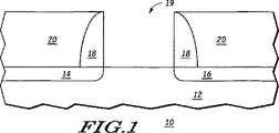
基板(12)にチャンネル領域を区画形成するよう分離された第1の電流電極(14)と第2の電流電極(16)を、基板に形成すること;
サイドウォールスペーサー(18)に包囲された基板(12)のチャンネル領域の上のダミースタックを除去することにより、サイドウォールスペーサー(18)内でかつ前記チャンネル領域の上に制御電極の位置を決定する制御電極溝を形成すること;および
制御電極溝の内に前記基板(12)のチャンネル領域を覆う制御電極スタックを形成すること;から成り、
前記制御電極スタックを形成することが、さらに、
制御電極溝の壁に直接隣接し、制御電極溝の第1の部分を占める制御電極誘電体(22)を、制御電極溝内におよび制御電極溝を超えて形成すること;
制御電極誘電体(22)に直接隣接し、制御電極溝の第2の部分を占め、トランジスタの閾値電圧値を決定する材料特性を有する制御電極層(24)を制御電極溝内におよび制御電極溝を超えて形成すること;
制御電極層に直接隣接し、制御電極溝の第3の部分を占め、トランジスタ構造の製造中に積層材料の選択的層除去のために使用される停止材料を提供する導電性停止層(26)を制御電極溝内におよび制御電極溝を超えて形成すること;
導電性停止層に直接隣接し、制御電極溝の第4の部分を占める導電層(28)を制御電極溝内におよび制御電極溝を超えて形成することであって、第1の部分、第2の部分、第3の部分、および第4の部分が、制御電極溝の開口部を実質的に占めること;
除去を停止する導電性停止層(26)を使用することにより、導電性停止層(26)の上部表面より上の導電層(28)を除去すること;および
実質的に平坦な上部表面を有するトランジスタの制御電極スタックを形成するために、前記サイドウォールスペーサー(18)の高さより上の導電層(28)、導電性停止層(26)、制御電極層(24)および制御電極誘電体(22)とを除去すること;から成る方法。 - 非平坦性の影響を最小限にする金属ゲート構造(10)をゲート溝内に形成する方法で
あって、
サイドウォールスペーサー(18)に包囲された基板(12)の上のダミースタックを除去することにより、サイドウォールスペーサー(18)内でかつ基板(12)の上にゲート溝を形成すること、
前記ゲート溝の全表面に隣接し、ゲート溝を超えて延びるゲート誘電体(22)を形成すること;
ゲート誘電体に隣接し、ゲート溝を超えて延び、ゲート溝の全体より少ない空間を占める、第1の金属から成るゲート電極層(24)を形成すること;
ゲート電極層の全露出面に隣接し、ゲート溝を超えて延び、ゲート電極層(24)と同様、ゲート溝の全体より少ない空間を占める、停止層(26)を形成すること;
停止層の全露出面に隣接し、ゲート溝を超えて延び、ゲート溝を実質的に占める、第2の金属から成る導電層(28)を形成すること;
実質的に除去を遅延させる停止層(26)を使用することにより、停止層(26)より上の導電層(28)のすべての部分を除去すること;および
サイドウォールスペーサー(18)の高さより上の導電層(28)、停止層(26)、ゲート電極層(24)およびゲート誘電体(22)のすべての部分を除去すること;から成る方法。
Applications Claiming Priority (2)
| Application Number | Priority Date | Filing Date | Title |
|---|---|---|---|
| US09/997,899 US6423619B1 (en) | 2001-11-30 | 2001-11-30 | Transistor metal gate structure that minimizes non-planarity effects and method of formation |
| PCT/US2002/036653 WO2003049186A2 (en) | 2001-11-30 | 2002-11-13 | Transistor metal gate structure that minimizes non-planarity effects and method of formation |
Publications (3)
| Publication Number | Publication Date |
|---|---|
| JP2005512326A JP2005512326A (ja) | 2005-04-28 |
| JP2005512326A5 JP2005512326A5 (ja) | 2006-01-05 |
| JP4159471B2 true JP4159471B2 (ja) | 2008-10-01 |
Family
ID=25544528
Family Applications (1)
| Application Number | Title | Priority Date | Filing Date |
|---|---|---|---|
| JP2003550282A Expired - Lifetime JP4159471B2 (ja) | 2001-11-30 | 2002-11-13 | 非平坦性の影響を最小限にするトランジスタ金属ゲート構造の製造方法 |
Country Status (8)
| Country | Link |
|---|---|
| US (1) | US6423619B1 (ja) |
| EP (1) | EP1451859A2 (ja) |
| JP (1) | JP4159471B2 (ja) |
| KR (1) | KR20040063971A (ja) |
| CN (1) | CN1306561C (ja) |
| AU (1) | AU2002365768A1 (ja) |
| TW (1) | TWI251345B (ja) |
| WO (1) | WO2003049186A2 (ja) |
Families Citing this family (74)
| Publication number | Priority date | Publication date | Assignee | Title |
|---|---|---|---|---|
| US6974766B1 (en) | 1998-10-01 | 2005-12-13 | Applied Materials, Inc. | In situ deposition of a low κ dielectric layer, barrier layer, etch stop, and anti-reflective coating for damascene application |
| US6620723B1 (en) | 2000-06-27 | 2003-09-16 | Applied Materials, Inc. | Formation of boride barrier layers using chemisorption techniques |
| US7101795B1 (en) | 2000-06-28 | 2006-09-05 | Applied Materials, Inc. | Method and apparatus for depositing refractory metal layers employing sequential deposition techniques to form a nucleation layer |
| US7732327B2 (en) | 2000-06-28 | 2010-06-08 | Applied Materials, Inc. | Vapor deposition of tungsten materials |
| US6551929B1 (en) | 2000-06-28 | 2003-04-22 | Applied Materials, Inc. | Bifurcated deposition process for depositing refractory metal layers employing atomic layer deposition and chemical vapor deposition techniques |
| US7405158B2 (en) | 2000-06-28 | 2008-07-29 | Applied Materials, Inc. | Methods for depositing tungsten layers employing atomic layer deposition techniques |
| US6936538B2 (en) | 2001-07-16 | 2005-08-30 | Applied Materials, Inc. | Method and apparatus for depositing tungsten after surface treatment to improve film characteristics |
| US7964505B2 (en) | 2005-01-19 | 2011-06-21 | Applied Materials, Inc. | Atomic layer deposition of tungsten materials |
| US6511911B1 (en) * | 2001-04-03 | 2003-01-28 | Advanced Micro Devices, Inc. | Metal gate stack with etch stop layer |
| US6849545B2 (en) * | 2001-06-20 | 2005-02-01 | Applied Materials, Inc. | System and method to form a composite film stack utilizing sequential deposition techniques |
| US7211144B2 (en) | 2001-07-13 | 2007-05-01 | Applied Materials, Inc. | Pulsed nucleation deposition of tungsten layers |
| WO2003029515A2 (en) * | 2001-07-16 | 2003-04-10 | Applied Materials, Inc. | Formation of composite tungsten films |
| US9051641B2 (en) | 2001-07-25 | 2015-06-09 | Applied Materials, Inc. | Cobalt deposition on barrier surfaces |
| US8110489B2 (en) | 2001-07-25 | 2012-02-07 | Applied Materials, Inc. | Process for forming cobalt-containing materials |
| US20090004850A1 (en) | 2001-07-25 | 2009-01-01 | Seshadri Ganguli | Process for forming cobalt and cobalt silicide materials in tungsten contact applications |
| TW589684B (en) * | 2001-10-10 | 2004-06-01 | Applied Materials Inc | Method for depositing refractory metal layers employing sequential deposition techniques |
| US6916398B2 (en) | 2001-10-26 | 2005-07-12 | Applied Materials, Inc. | Gas delivery apparatus and method for atomic layer deposition |
| US7780785B2 (en) | 2001-10-26 | 2010-08-24 | Applied Materials, Inc. | Gas delivery apparatus for atomic layer deposition |
| US6809026B2 (en) | 2001-12-21 | 2004-10-26 | Applied Materials, Inc. | Selective deposition of a barrier layer on a metal film |
| EP1324393B1 (en) * | 2001-12-28 | 2008-04-09 | STMicroelectronics S.r.l. | Manufacturing process of a semiconductor non-volatile memory cell and corresponding memory-cell |
| US6894355B1 (en) * | 2002-01-11 | 2005-05-17 | Advanced Micro Devices, Inc. | Semiconductor device with silicide source/drain and high-K dielectric |
| US6911391B2 (en) | 2002-01-26 | 2005-06-28 | Applied Materials, Inc. | Integration of titanium and titanium nitride layers |
| US6998014B2 (en) | 2002-01-26 | 2006-02-14 | Applied Materials, Inc. | Apparatus and method for plasma assisted deposition |
| US6827978B2 (en) | 2002-02-11 | 2004-12-07 | Applied Materials, Inc. | Deposition of tungsten films |
| US6833161B2 (en) | 2002-02-26 | 2004-12-21 | Applied Materials, Inc. | Cyclical deposition of tungsten nitride for metal oxide gate electrode |
| US6720027B2 (en) * | 2002-04-08 | 2004-04-13 | Applied Materials, Inc. | Cyclical deposition of a variable content titanium silicon nitride layer |
| KR100476556B1 (ko) * | 2002-04-11 | 2005-03-18 | 삼성전기주식회사 | 압전트랜스 장치, 압전트랜스 하우징 및 그 제조방법 |
| US7279432B2 (en) * | 2002-04-16 | 2007-10-09 | Applied Materials, Inc. | System and method for forming an integrated barrier layer |
| US7264846B2 (en) * | 2002-06-04 | 2007-09-04 | Applied Materials, Inc. | Ruthenium layer formation for copper film deposition |
| US7404985B2 (en) * | 2002-06-04 | 2008-07-29 | Applied Materials, Inc. | Noble metal layer formation for copper film deposition |
| US7910165B2 (en) * | 2002-06-04 | 2011-03-22 | Applied Materials, Inc. | Ruthenium layer formation for copper film deposition |
| US6838125B2 (en) | 2002-07-10 | 2005-01-04 | Applied Materials, Inc. | Method of film deposition using activated precursor gases |
| US20040036129A1 (en) * | 2002-08-22 | 2004-02-26 | Micron Technology, Inc. | Atomic layer deposition of CMOS gates with variable work functions |
| US6821563B2 (en) | 2002-10-02 | 2004-11-23 | Applied Materials, Inc. | Gas distribution system for cyclical layer deposition |
| US6924184B2 (en) * | 2003-03-21 | 2005-08-02 | Freescale Semiconductor, Inc. | Semiconductor device and method for forming a semiconductor device using post gate stack planarization |
| US6686282B1 (en) | 2003-03-31 | 2004-02-03 | Motorola, Inc. | Plated metal transistor gate and method of formation |
| US7071086B2 (en) * | 2003-04-23 | 2006-07-04 | Advanced Micro Devices, Inc. | Method of forming a metal gate structure with tuning of work function by silicon incorporation |
| WO2004113585A2 (en) | 2003-06-18 | 2004-12-29 | Applied Materials, Inc. | Atomic layer deposition of barrier materials |
| US20050104142A1 (en) * | 2003-11-13 | 2005-05-19 | Vijav Narayanan | CVD tantalum compounds for FET get electrodes |
| US20050181226A1 (en) * | 2004-01-26 | 2005-08-18 | Applied Materials, Inc. | Method and apparatus for selectively changing thin film composition during electroless deposition in a single chamber |
| US7205234B2 (en) | 2004-02-05 | 2007-04-17 | Taiwan Semiconductor Manufacturing Company, Ltd. | Method of forming metal silicide |
| US20050253268A1 (en) * | 2004-04-22 | 2005-11-17 | Shao-Ta Hsu | Method and structure for improving adhesion between intermetal dielectric layer and cap layer |
| US8323754B2 (en) | 2004-05-21 | 2012-12-04 | Applied Materials, Inc. | Stabilization of high-k dielectric materials |
| US7429402B2 (en) * | 2004-12-10 | 2008-09-30 | Applied Materials, Inc. | Ruthenium as an underlayer for tungsten film deposition |
| US7265048B2 (en) * | 2005-03-01 | 2007-09-04 | Applied Materials, Inc. | Reduction of copper dewetting by transition metal deposition |
| US7432139B2 (en) * | 2005-06-29 | 2008-10-07 | Amberwave Systems Corp. | Methods for forming dielectrics and metal electrodes |
| US7473637B2 (en) | 2005-07-20 | 2009-01-06 | Micron Technology, Inc. | ALD formed titanium nitride films |
| JP2007073637A (ja) * | 2005-09-05 | 2007-03-22 | Tokyo Electron Ltd | 成膜方法および半導体装置の製造方法 |
| TWI332532B (en) | 2005-11-04 | 2010-11-01 | Applied Materials Inc | Apparatus and process for plasma-enhanced atomic layer deposition |
| US7709402B2 (en) | 2006-02-16 | 2010-05-04 | Micron Technology, Inc. | Conductive layers for hafnium silicon oxynitride films |
| US7833358B2 (en) * | 2006-04-07 | 2010-11-16 | Applied Materials, Inc. | Method of recovering valuable material from exhaust gas stream of a reaction chamber |
| US8193641B2 (en) * | 2006-05-09 | 2012-06-05 | Intel Corporation | Recessed workfunction metal in CMOS transistor gates |
| US7655550B2 (en) * | 2006-06-30 | 2010-02-02 | Freescale Semiconductor, Inc. | Method of making metal gate transistors |
| JP2008171872A (ja) * | 2007-01-09 | 2008-07-24 | Elpida Memory Inc | 半導体装置及びその製造方法 |
| US7737028B2 (en) * | 2007-09-28 | 2010-06-15 | Applied Materials, Inc. | Selective ruthenium deposition on copper materials |
| US8022472B2 (en) * | 2007-12-04 | 2011-09-20 | Rohm Co., Ltd. | Semiconductor device and method of manufacturing semiconductor device |
| US7964487B2 (en) * | 2008-06-04 | 2011-06-21 | International Business Machines Corporation | Carrier mobility enhanced channel devices and method of manufacture |
| US8524588B2 (en) | 2008-08-18 | 2013-09-03 | Taiwan Semiconductor Manufacturing Company, Ltd. | Method of forming a single metal that performs N work function and P work function in a high-k/metal gate process |
| KR101574107B1 (ko) | 2010-02-11 | 2015-12-04 | 삼성전자 주식회사 | 반도체 장치의 제조 방법 |
| JP5937297B2 (ja) * | 2010-03-01 | 2016-06-22 | キヤノンアネルバ株式会社 | 金属窒化膜、該金属窒化膜を用いた半導体装置、および半導体装置の製造方法 |
| JP5598145B2 (ja) * | 2010-08-04 | 2014-10-01 | 富士通セミコンダクター株式会社 | 半導体装置の製造方法及び半導体装置 |
| CN102437032B (zh) * | 2010-09-29 | 2015-04-01 | 中国科学院微电子研究所 | 后栅工艺中金属栅的制作方法 |
| KR101746709B1 (ko) * | 2010-11-24 | 2017-06-14 | 삼성전자주식회사 | 금속 게이트 전극들을 갖는 반도체 소자의 제조방법 |
| US8759219B2 (en) * | 2011-01-24 | 2014-06-24 | United Microelectronics Corp. | Planarization method applied in process of manufacturing semiconductor component |
| TWI512797B (zh) * | 2011-01-24 | 2015-12-11 | United Microelectronics Corp | 應用於半導體元件製程中之平坦化方法 |
| CN102646580B (zh) * | 2011-02-18 | 2016-10-05 | 联华电子股份有限公司 | 应用于半导体元件工艺中的平坦化方法以及栅极构造 |
| US8865594B2 (en) * | 2011-03-10 | 2014-10-21 | Applied Materials, Inc. | Formation of liner and barrier for tungsten as gate electrode and as contact plug to reduce resistance and enhance device performance |
| US20130075831A1 (en) * | 2011-09-24 | 2013-03-28 | Taiwan Semiconductor Manufacturing Company, Ltd. | Metal gate stack having tialn blocking/wetting layer |
| US8901665B2 (en) * | 2011-12-22 | 2014-12-02 | Taiwan Semiconductor Manufacturing Company, Ltd. | Gate structure for semiconductor device |
| US9324710B2 (en) | 2014-02-24 | 2016-04-26 | International Business Machines Corporation | Very planar gate cut post replacement gate process |
| US9583486B1 (en) * | 2015-11-19 | 2017-02-28 | International Business Machines Corporation | Stable work function for narrow-pitch devices |
| TWI633660B (zh) * | 2017-05-22 | 2018-08-21 | Powerchip Technology Corporation | 半導體元件及其製造方法 |
| CN109309003A (zh) * | 2017-07-26 | 2019-02-05 | 中芯国际集成电路制造(上海)有限公司 | 鳍式场效应晶体管的形成方法 |
| US11152222B2 (en) | 2019-08-06 | 2021-10-19 | Taiwan Semiconductor Manufacturing Company, Ltd. | Dishing prevention structure embedded in a gate electrode |
Family Cites Families (16)
| Publication number | Priority date | Publication date | Assignee | Title |
|---|---|---|---|---|
| US5494857A (en) * | 1993-07-28 | 1996-02-27 | Digital Equipment Corporation | Chemical mechanical planarization of shallow trenches in semiconductor substrates |
| US5604159A (en) | 1994-01-31 | 1997-02-18 | Motorola, Inc. | Method of making a contact structure |
| US5364817A (en) | 1994-05-05 | 1994-11-15 | United Microelectronics Corporation | Tungsten-plug process |
| US5654589A (en) | 1995-06-06 | 1997-08-05 | Advanced Micro Devices, Incorporated | Landing pad technology doubled up as local interconnect and borderless contact for deep sub-half micrometer IC application |
| US6040599A (en) * | 1996-03-12 | 2000-03-21 | Mitsubishi Denki Kabushiki Kaisha | Insulated trench semiconductor device with particular layer structure |
| US6015757A (en) * | 1997-07-02 | 2000-01-18 | Taiwan Semiconductor Manufacturing Co. Ltd. | Method of oxide etching with high selectivity to silicon nitride by using polysilicon layer |
| US5966597A (en) * | 1998-01-06 | 1999-10-12 | Altera Corporation | Method of forming low resistance gate electrodes |
| TW379406B (en) * | 1998-04-27 | 2000-01-11 | United Microelectronics Corp | Shallow trench isolation method |
| US6150260A (en) | 1998-07-06 | 2000-11-21 | Chartered Semiconductor Manufacturing Ltd. | Sacrificial stop layer and endpoint for metal CMP |
| US6140224A (en) | 1999-04-19 | 2000-10-31 | Worldiwide Semiconductor Manufacturing Corporation | Method of forming a tungsten plug |
| JP4237332B2 (ja) * | 1999-04-30 | 2009-03-11 | 株式会社東芝 | 半導体装置の製造方法 |
| JP2000332242A (ja) * | 1999-05-21 | 2000-11-30 | Mitsubishi Electric Corp | 半導体装置及びその製造方法 |
| US6171910B1 (en) | 1999-07-21 | 2001-01-09 | Motorola Inc. | Method for forming a semiconductor device |
| US6087231A (en) | 1999-08-05 | 2000-07-11 | Advanced Micro Devices, Inc. | Fabrication of dual gates of field transistors with prevention of reaction between the gate electrode and the gate dielectric with a high dielectric constant |
| US6248675B1 (en) * | 1999-08-05 | 2001-06-19 | Advanced Micro Devices, Inc. | Fabrication of field effect transistors having dual gates with gate dielectrics of high dielectric constant using lowered temperatures |
| US6200886B1 (en) | 1999-10-28 | 2001-03-13 | United Silicon Incorporated | Fabricating process for polysilicon gate |
-
2001
- 2001-11-30 US US09/997,899 patent/US6423619B1/en not_active Expired - Lifetime
-
2002
- 2002-11-13 EP EP02804420A patent/EP1451859A2/en not_active Withdrawn
- 2002-11-13 JP JP2003550282A patent/JP4159471B2/ja not_active Expired - Lifetime
- 2002-11-13 WO PCT/US2002/036653 patent/WO2003049186A2/en active Application Filing
- 2002-11-13 AU AU2002365768A patent/AU2002365768A1/en not_active Abandoned
- 2002-11-13 CN CNB028236610A patent/CN1306561C/zh not_active Expired - Lifetime
- 2002-11-13 KR KR10-2004-7007928A patent/KR20040063971A/ko not_active Application Discontinuation
- 2002-11-29 TW TW091134782A patent/TWI251345B/zh not_active IP Right Cessation
Also Published As
| Publication number | Publication date |
|---|---|
| KR20040063971A (ko) | 2004-07-15 |
| CN1306561C (zh) | 2007-03-21 |
| CN1596460A (zh) | 2005-03-16 |
| TW200300609A (en) | 2003-06-01 |
| EP1451859A2 (en) | 2004-09-01 |
| AU2002365768A8 (en) | 2003-06-17 |
| AU2002365768A1 (en) | 2003-06-17 |
| WO2003049186A3 (en) | 2003-09-12 |
| US6423619B1 (en) | 2002-07-23 |
| WO2003049186A2 (en) | 2003-06-12 |
| JP2005512326A (ja) | 2005-04-28 |
| TWI251345B (en) | 2006-03-11 |
Similar Documents
| Publication | Publication Date | Title |
|---|---|---|
| JP4159471B2 (ja) | 非平坦性の影響を最小限にするトランジスタ金属ゲート構造の製造方法 | |
| KR102136176B1 (ko) | 금속 게이트의 절단 방법 및 그 금속 게이트가 형성된 구조물 | |
| KR102254439B1 (ko) | 반도체 장치 | |
| KR20190024625A (ko) | 반도체 디바이스 및 방법 | |
| CN110088906B (zh) | 三维存储器件中的高k电介质层及其形成方法 | |
| US20140264480A1 (en) | Semiconductor device and method of forming the same | |
| US9379209B2 (en) | Selectively forming a protective conductive cap on a metal gate electrode | |
| US9859273B2 (en) | Semiconductor structure and manufacturing process thereof | |
| US11587796B2 (en) | 3D-NAND memory cell structure | |
| US9034759B2 (en) | Method for forming interlevel dielectric (ILD) layer | |
| CN113632231A (zh) | 3-d nand模具 | |
| JP2023531202A (ja) | 閉じ込められた電荷トラップ層 | |
| CN113380899A (zh) | 半导体结构、晶体管和形成晶体管器件的方法 | |
| US10283412B2 (en) | Semiconductor device and fabrication method thereof | |
| TWI579928B (zh) | 形成層間介電層的方法 | |
| US20220319601A1 (en) | Selection gate separation for 3d nand | |
| US20220059555A1 (en) | Selection gate separation for 3d nand | |
| US20230040627A1 (en) | Selection gate structure and fabrication method for 3d memory | |
| US20180366552A1 (en) | Semiconductor device |
Legal Events
| Date | Code | Title | Description |
|---|---|---|---|
| A521 | Request for written amendment filed |
Free format text: JAPANESE INTERMEDIATE CODE: A523 Effective date: 20051007 |
|
| A621 | Written request for application examination |
Free format text: JAPANESE INTERMEDIATE CODE: A621 Effective date: 20051007 |
|
| A977 | Report on retrieval |
Free format text: JAPANESE INTERMEDIATE CODE: A971007 Effective date: 20070717 |
|
| A131 | Notification of reasons for refusal |
Free format text: JAPANESE INTERMEDIATE CODE: A131 Effective date: 20070724 |
|
| A521 | Request for written amendment filed |
Free format text: JAPANESE INTERMEDIATE CODE: A523 Effective date: 20071012 |
|
| A02 | Decision of refusal |
Free format text: JAPANESE INTERMEDIATE CODE: A02 Effective date: 20071106 |
|
| A521 | Request for written amendment filed |
Free format text: JAPANESE INTERMEDIATE CODE: A523 Effective date: 20080109 |
|
| A911 | Transfer to examiner for re-examination before appeal (zenchi) |
Free format text: JAPANESE INTERMEDIATE CODE: A911 Effective date: 20080304 |
|
| A131 | Notification of reasons for refusal |
Free format text: JAPANESE INTERMEDIATE CODE: A131 Effective date: 20080325 |
|
| A521 | Request for written amendment filed |
Free format text: JAPANESE INTERMEDIATE CODE: A523 Effective date: 20080530 |
|
| TRDD | Decision of grant or rejection written | ||
| A01 | Written decision to grant a patent or to grant a registration (utility model) |
Free format text: JAPANESE INTERMEDIATE CODE: A01 Effective date: 20080617 |
|
| A01 | Written decision to grant a patent or to grant a registration (utility model) |
Free format text: JAPANESE INTERMEDIATE CODE: A01 |
|
| A61 | First payment of annual fees (during grant procedure) |
Free format text: JAPANESE INTERMEDIATE CODE: A61 Effective date: 20080715 |
|
| R150 | Certificate of patent or registration of utility model |
Free format text: JAPANESE INTERMEDIATE CODE: R150 Ref document number: 4159471 Country of ref document: JP Free format text: JAPANESE INTERMEDIATE CODE: R150 |
|
| FPAY | Renewal fee payment (event date is renewal date of database) |
Free format text: PAYMENT UNTIL: 20110725 Year of fee payment: 3 |
|
| FPAY | Renewal fee payment (event date is renewal date of database) |
Free format text: PAYMENT UNTIL: 20110725 Year of fee payment: 3 |
|
| FPAY | Renewal fee payment (event date is renewal date of database) |
Free format text: PAYMENT UNTIL: 20120725 Year of fee payment: 4 |
|
| R250 | Receipt of annual fees |
Free format text: JAPANESE INTERMEDIATE CODE: R250 |
|
| FPAY | Renewal fee payment (event date is renewal date of database) |
Free format text: PAYMENT UNTIL: 20120725 Year of fee payment: 4 |
|
| FPAY | Renewal fee payment (event date is renewal date of database) |
Free format text: PAYMENT UNTIL: 20130725 Year of fee payment: 5 |
|
| R250 | Receipt of annual fees |
Free format text: JAPANESE INTERMEDIATE CODE: R250 |
|
| R250 | Receipt of annual fees |
Free format text: JAPANESE INTERMEDIATE CODE: R250 |
|
| R250 | Receipt of annual fees |
Free format text: JAPANESE INTERMEDIATE CODE: R250 |
|
| R250 | Receipt of annual fees |
Free format text: JAPANESE INTERMEDIATE CODE: R250 |
|
| R250 | Receipt of annual fees |
Free format text: JAPANESE INTERMEDIATE CODE: R250 |
|
| R250 | Receipt of annual fees |
Free format text: JAPANESE INTERMEDIATE CODE: R250 |
|
| S533 | Written request for registration of change of name |
Free format text: JAPANESE INTERMEDIATE CODE: R313533 |
|
| R350 | Written notification of registration of transfer |
Free format text: JAPANESE INTERMEDIATE CODE: R350 |
|
| R250 | Receipt of annual fees |
Free format text: JAPANESE INTERMEDIATE CODE: R250 |
|
| R250 | Receipt of annual fees |
Free format text: JAPANESE INTERMEDIATE CODE: R250 |
|
| R250 | Receipt of annual fees |
Free format text: JAPANESE INTERMEDIATE CODE: R250 |
|
| R250 | Receipt of annual fees |
Free format text: JAPANESE INTERMEDIATE CODE: R250 |
|
| R250 | Receipt of annual fees |
Free format text: JAPANESE INTERMEDIATE CODE: R250 |
|
| EXPY | Cancellation because of completion of term |