JP4145437B2 - Single crystal GaN crystal growth method, single crystal GaN substrate manufacturing method, and single crystal GaN substrate - Google Patents
Single crystal GaN crystal growth method, single crystal GaN substrate manufacturing method, and single crystal GaN substrate Download PDFInfo
- Publication number
- JP4145437B2 JP4145437B2 JP27388299A JP27388299A JP4145437B2 JP 4145437 B2 JP4145437 B2 JP 4145437B2 JP 27388299 A JP27388299 A JP 27388299A JP 27388299 A JP27388299 A JP 27388299A JP 4145437 B2 JP4145437 B2 JP 4145437B2
- Authority
- JP
- Japan
- Prior art keywords
- growth
- gan
- facet
- crystal
- single crystal
- Prior art date
- Legal status (The legal status is an assumption and is not a legal conclusion. Google has not performed a legal analysis and makes no representation as to the accuracy of the status listed.)
- Expired - Fee Related
Links
- 239000013078 crystal Substances 0.000 title claims description 242
- JMASRVWKEDWRBT-UHFFFAOYSA-N Gallium nitride Chemical compound [Ga]#N JMASRVWKEDWRBT-UHFFFAOYSA-N 0.000 title claims description 57
- 238000004519 manufacturing process Methods 0.000 title claims description 29
- 238000002109 crystal growth method Methods 0.000 title claims description 26
- 239000000758 substrate Substances 0.000 claims description 219
- 230000007547 defect Effects 0.000 claims description 107
- 238000000034 method Methods 0.000 claims description 67
- 229910052594 sapphire Inorganic materials 0.000 claims description 62
- 239000010980 sapphire Substances 0.000 claims description 62
- 229910001218 Gallium arsenide Inorganic materials 0.000 claims description 59
- 238000001947 vapour-phase growth Methods 0.000 claims description 46
- 238000002248 hydride vapour-phase epitaxy Methods 0.000 claims description 25
- 230000002829 reductive effect Effects 0.000 claims description 24
- 230000015572 biosynthetic process Effects 0.000 claims description 14
- 239000002131 composite material Substances 0.000 claims description 14
- 229910052596 spinel Inorganic materials 0.000 claims description 13
- 238000000227 grinding Methods 0.000 claims description 12
- 229910005540 GaP Inorganic materials 0.000 claims description 11
- 239000011029 spinel Substances 0.000 claims description 11
- 238000005498 polishing Methods 0.000 claims description 9
- 229910004298 SiO 2 Inorganic materials 0.000 claims description 7
- 238000005530 etching Methods 0.000 claims description 6
- 238000012545 processing Methods 0.000 claims description 6
- 238000005520 cutting process Methods 0.000 claims description 5
- 230000002776 aggregation Effects 0.000 claims description 4
- 238000004220 aggregation Methods 0.000 claims description 4
- CPLXHLVBOLITMK-UHFFFAOYSA-N magnesium oxide Inorganic materials [Mg]=O CPLXHLVBOLITMK-UHFFFAOYSA-N 0.000 claims description 4
- XLOMVQKBTHCTTD-UHFFFAOYSA-N zinc oxide Inorganic materials [Zn]=O XLOMVQKBTHCTTD-UHFFFAOYSA-N 0.000 claims description 4
- -1 NdGaO 3 Substances 0.000 claims 6
- 239000012141 concentrate Substances 0.000 claims 5
- 229910002601 GaN Inorganic materials 0.000 description 218
- 238000001652 electrophoretic deposition Methods 0.000 description 73
- 229920001345 ε-poly-D-lysine Polymers 0.000 description 73
- 235000012431 wafers Nutrition 0.000 description 50
- 230000036961 partial effect Effects 0.000 description 42
- VEXZGXHMUGYJMC-UHFFFAOYSA-N Hydrochloric acid Chemical compound Cl VEXZGXHMUGYJMC-UHFFFAOYSA-N 0.000 description 35
- 230000009467 reduction Effects 0.000 description 24
- 230000000694 effects Effects 0.000 description 19
- 239000010408 film Substances 0.000 description 16
- 239000004065 semiconductor Substances 0.000 description 14
- 208000012868 Overgrowth Diseases 0.000 description 12
- 230000008569 process Effects 0.000 description 12
- VYPSYNLAJGMNEJ-UHFFFAOYSA-N Silicium dioxide Chemical compound O=[Si]=O VYPSYNLAJGMNEJ-UHFFFAOYSA-N 0.000 description 9
- 230000005540 biological transmission Effects 0.000 description 9
- 230000007423 decrease Effects 0.000 description 9
- 239000007789 gas Substances 0.000 description 9
- 239000000463 material Substances 0.000 description 9
- 238000003776 cleavage reaction Methods 0.000 description 8
- 230000006870 function Effects 0.000 description 8
- 230000007246 mechanism Effects 0.000 description 8
- 230000007017 scission Effects 0.000 description 8
- 229910052681 coesite Inorganic materials 0.000 description 7
- 229910052906 cristobalite Inorganic materials 0.000 description 7
- 239000000377 silicon dioxide Substances 0.000 description 7
- 229910052682 stishovite Inorganic materials 0.000 description 7
- 239000010409 thin film Substances 0.000 description 7
- 229910052905 tridymite Inorganic materials 0.000 description 7
- 239000012808 vapor phase Substances 0.000 description 7
- 238000005136 cathodoluminescence Methods 0.000 description 6
- 230000008859 change Effects 0.000 description 6
- 229910017083 AlN Inorganic materials 0.000 description 5
- 229910003200 NdGaO3 Inorganic materials 0.000 description 5
- XOYLJNJLGBYDTH-UHFFFAOYSA-M chlorogallium Chemical compound [Ga]Cl XOYLJNJLGBYDTH-UHFFFAOYSA-M 0.000 description 5
- NBIIXXVUZAFLBC-UHFFFAOYSA-N Phosphoric acid Chemical compound OP(O)(O)=O NBIIXXVUZAFLBC-UHFFFAOYSA-N 0.000 description 4
- QAOWNCQODCNURD-UHFFFAOYSA-N Sulfuric acid Chemical compound OS(O)(=O)=O QAOWNCQODCNURD-UHFFFAOYSA-N 0.000 description 4
- 239000012159 carrier gas Substances 0.000 description 4
- 229910052751 metal Inorganic materials 0.000 description 4
- 239000002184 metal Substances 0.000 description 4
- 230000008719 thickening Effects 0.000 description 4
- 230000003247 decreasing effect Effects 0.000 description 3
- 238000009826 distribution Methods 0.000 description 3
- 238000010191 image analysis Methods 0.000 description 3
- 238000005259 measurement Methods 0.000 description 3
- UFHFLCQGNIYNRP-UHFFFAOYSA-N Hydrogen Chemical compound [H][H] UFHFLCQGNIYNRP-UHFFFAOYSA-N 0.000 description 2
- 229910020068 MgAl Inorganic materials 0.000 description 2
- 229910026161 MgAl2O4 Inorganic materials 0.000 description 2
- 239000002253 acid Substances 0.000 description 2
- 230000009471 action Effects 0.000 description 2
- 229910000147 aluminium phosphate Inorganic materials 0.000 description 2
- QZPSXPBJTPJTSZ-UHFFFAOYSA-N aqua regia Chemical compound Cl.O[N+]([O-])=O QZPSXPBJTPJTSZ-UHFFFAOYSA-N 0.000 description 2
- 230000008901 benefit Effects 0.000 description 2
- 238000007796 conventional method Methods 0.000 description 2
- 238000000151 deposition Methods 0.000 description 2
- 238000011156 evaluation Methods 0.000 description 2
- 238000002474 experimental method Methods 0.000 description 2
- 238000010438 heat treatment Methods 0.000 description 2
- 238000003754 machining Methods 0.000 description 2
- 238000001000 micrograph Methods 0.000 description 2
- 150000004767 nitrides Chemical class 0.000 description 2
- 238000000206 photolithography Methods 0.000 description 2
- 238000005268 plasma chemical vapour deposition Methods 0.000 description 2
- VEXZGXHMUGYJMC-UHFFFAOYSA-M Chloride anion Chemical compound [Cl-] VEXZGXHMUGYJMC-UHFFFAOYSA-M 0.000 description 1
- 101000574352 Mus musculus Protein phosphatase 1 regulatory subunit 17 Proteins 0.000 description 1
- 230000001133 acceleration Effects 0.000 description 1
- 238000009825 accumulation Methods 0.000 description 1
- 230000002411 adverse Effects 0.000 description 1
- 238000013459 approach Methods 0.000 description 1
- 229910052785 arsenic Inorganic materials 0.000 description 1
- RQNWIZPPADIBDY-UHFFFAOYSA-N arsenic atom Chemical compound [As] RQNWIZPPADIBDY-UHFFFAOYSA-N 0.000 description 1
- 238000005452 bending Methods 0.000 description 1
- 238000006243 chemical reaction Methods 0.000 description 1
- 235000019219 chocolate Nutrition 0.000 description 1
- 239000011248 coating agent Substances 0.000 description 1
- 238000000576 coating method Methods 0.000 description 1
- 150000001875 compounds Chemical class 0.000 description 1
- 238000011109 contamination Methods 0.000 description 1
- 238000001816 cooling Methods 0.000 description 1
- 230000006866 deterioration Effects 0.000 description 1
- 238000002050 diffraction method Methods 0.000 description 1
- 238000009792 diffusion process Methods 0.000 description 1
- 238000010894 electron beam technology Methods 0.000 description 1
- 230000008030 elimination Effects 0.000 description 1
- 238000003379 elimination reaction Methods 0.000 description 1
- 239000001257 hydrogen Substances 0.000 description 1
- 229910052739 hydrogen Inorganic materials 0.000 description 1
- 239000012535 impurity Substances 0.000 description 1
- 238000009776 industrial production Methods 0.000 description 1
- 230000003993 interaction Effects 0.000 description 1
- 239000007791 liquid phase Substances 0.000 description 1
- 238000004020 luminiscence type Methods 0.000 description 1
- 238000000691 measurement method Methods 0.000 description 1
- 239000000155 melt Substances 0.000 description 1
- 229910003465 moissanite Inorganic materials 0.000 description 1
- 238000005457 optimization Methods 0.000 description 1
- TWNQGVIAIRXVLR-UHFFFAOYSA-N oxo(oxoalumanyloxy)alumane Chemical compound O=[Al]O[Al]=O TWNQGVIAIRXVLR-UHFFFAOYSA-N 0.000 description 1
- 230000002265 prevention Effects 0.000 description 1
- 239000002994 raw material Substances 0.000 description 1
- 230000002441 reversible effect Effects 0.000 description 1
- 229910010271 silicon carbide Inorganic materials 0.000 description 1
- 239000007787 solid Substances 0.000 description 1
- 239000007790 solid phase Substances 0.000 description 1
- 238000005092 sublimation method Methods 0.000 description 1
- 239000000126 substance Substances 0.000 description 1
- 238000005308 sum rule Methods 0.000 description 1
- 230000003746 surface roughness Effects 0.000 description 1
- 230000008646 thermal stress Effects 0.000 description 1
- 230000007704 transition Effects 0.000 description 1
- 230000001960 triggered effect Effects 0.000 description 1
- 238000011144 upstream manufacturing Methods 0.000 description 1
- 238000000927 vapour-phase epitaxy Methods 0.000 description 1
- 238000001039 wet etching Methods 0.000 description 1
Images


Classifications
-
- C—CHEMISTRY; METALLURGY
- C30—CRYSTAL GROWTH
- C30B—SINGLE-CRYSTAL GROWTH; UNIDIRECTIONAL SOLIDIFICATION OF EUTECTIC MATERIAL OR UNIDIRECTIONAL DEMIXING OF EUTECTOID MATERIAL; REFINING BY ZONE-MELTING OF MATERIAL; PRODUCTION OF A HOMOGENEOUS POLYCRYSTALLINE MATERIAL WITH DEFINED STRUCTURE; SINGLE CRYSTALS OR HOMOGENEOUS POLYCRYSTALLINE MATERIAL WITH DEFINED STRUCTURE; AFTER-TREATMENT OF SINGLE CRYSTALS OR A HOMOGENEOUS POLYCRYSTALLINE MATERIAL WITH DEFINED STRUCTURE; APPARATUS THEREFOR
- C30B25/00—Single-crystal growth by chemical reaction of reactive gases, e.g. chemical vapour-deposition growth
- C30B25/02—Epitaxial-layer growth
-
- C—CHEMISTRY; METALLURGY
- C30—CRYSTAL GROWTH
- C30B—SINGLE-CRYSTAL GROWTH; UNIDIRECTIONAL SOLIDIFICATION OF EUTECTIC MATERIAL OR UNIDIRECTIONAL DEMIXING OF EUTECTOID MATERIAL; REFINING BY ZONE-MELTING OF MATERIAL; PRODUCTION OF A HOMOGENEOUS POLYCRYSTALLINE MATERIAL WITH DEFINED STRUCTURE; SINGLE CRYSTALS OR HOMOGENEOUS POLYCRYSTALLINE MATERIAL WITH DEFINED STRUCTURE; AFTER-TREATMENT OF SINGLE CRYSTALS OR A HOMOGENEOUS POLYCRYSTALLINE MATERIAL WITH DEFINED STRUCTURE; APPARATUS THEREFOR
- C30B29/00—Single crystals or homogeneous polycrystalline material with defined structure characterised by the material or by their shape
- C30B29/10—Inorganic compounds or compositions
- C30B29/40—AIIIBV compounds wherein A is B, Al, Ga, In or Tl and B is N, P, As, Sb or Bi
- C30B29/403—AIII-nitrides
- C30B29/406—Gallium nitride
-
- C—CHEMISTRY; METALLURGY
- C30—CRYSTAL GROWTH
- C30B—SINGLE-CRYSTAL GROWTH; UNIDIRECTIONAL SOLIDIFICATION OF EUTECTIC MATERIAL OR UNIDIRECTIONAL DEMIXING OF EUTECTOID MATERIAL; REFINING BY ZONE-MELTING OF MATERIAL; PRODUCTION OF A HOMOGENEOUS POLYCRYSTALLINE MATERIAL WITH DEFINED STRUCTURE; SINGLE CRYSTALS OR HOMOGENEOUS POLYCRYSTALLINE MATERIAL WITH DEFINED STRUCTURE; AFTER-TREATMENT OF SINGLE CRYSTALS OR A HOMOGENEOUS POLYCRYSTALLINE MATERIAL WITH DEFINED STRUCTURE; APPARATUS THEREFOR
- C30B33/00—After-treatment of single crystals or homogeneous polycrystalline material with defined structure
-
- H—ELECTRICITY
- H10—SEMICONDUCTOR DEVICES; ELECTRIC SOLID-STATE DEVICES NOT OTHERWISE PROVIDED FOR
- H10H—INORGANIC LIGHT-EMITTING SEMICONDUCTOR DEVICES HAVING POTENTIAL BARRIERS
- H10H20/00—Individual inorganic light-emitting semiconductor devices having potential barriers, e.g. light-emitting diodes [LED]
- H10H20/01—Manufacture or treatment
- H10H20/011—Manufacture or treatment of bodies, e.g. forming semiconductor layers
- H10H20/013—Manufacture or treatment of bodies, e.g. forming semiconductor layers having light-emitting regions comprising only Group III-V materials
- H10H20/0137—Manufacture or treatment of bodies, e.g. forming semiconductor layers having light-emitting regions comprising only Group III-V materials the light-emitting regions comprising nitride materials
Landscapes
- Chemical & Material Sciences (AREA)
- Engineering & Computer Science (AREA)
- Crystallography & Structural Chemistry (AREA)
- Materials Engineering (AREA)
- Metallurgy (AREA)
- Organic Chemistry (AREA)
- Inorganic Chemistry (AREA)
- Chemical Kinetics & Catalysis (AREA)
- General Chemical & Material Sciences (AREA)
- Crystals, And After-Treatments Of Crystals (AREA)
- Led Devices (AREA)
- Semiconductor Lasers (AREA)
Description
【0001】
【産業上の利用分野】
この発明は、3−5族化合物半導体からなる発光ダイオード(LED)、レ−ザ(LD)などの発光デバイスなどに用いられるGaN単結晶基板、およびその結晶成長方法、製造方法に関する。
【0002】
【従来の技術】
3−5族窒化物系半導体(GaN、GaInN)を用いた発光デバイスは、青色LEDなどで既に実用化されている。広いGaN基板が得られないため、窒化物半導体発光デバイスは、基板としてもっぱらサファイアが用いられてきた。サファイア(Al2O3)は(0001)面が6回対称性を持ち、その上にGaN単結晶の薄膜が成長する。サファイア上のGaN薄膜、GaInN薄膜は転位が極めて多い。が、それでも青色LEDとして利用でき寿命も長い。サファイアは化学的にも物理的にも堅牢であり耐熱性もある。非常に硬く安定な基板材料である。このような長所があるからGaInN系青色LEDの基板として、サファイア基板が独占的に使われる。
【0003】
ところがサファイア基板には次のような問題点がある。サファイア基板には劈開面がない。しかも極めて硬い材料である。ウエハ上に多数のLED素子を製造しチップに分割するとき通常の半導体のように劈開面で自然に割るというわけにいかない。機械的手段(ダイシング)でウエハを縦横に切断してチップとするしかない。ダイシング工程がコストを押し上げる。半導体レ−ザとする場合はさらに劈開によって反射面を作成することができない。そのため品質面で問題があった。さらに反射面作製のためのコスト高を招くという欠点があった。さらにサファイアは絶縁性基板である。
【0004】
これもさまざまな問題を引き起こす。絶縁性だから、通常のLEDのように基板底面を電極とすることができない。ためにデバイスの上下面に電極を作るということができない。デバイスの一部をエッチングで除去しGaN下層部を露出させ、これをn電極とする必要がある。リードと電極の接続のために2回ワイヤボンディングしなければならない。下側電極を取り付ける半導体層には横方向に電流が流れるが抵抗を下げるためある程度の層の厚みがなくてはならない。ために下側半導体層が厚くなる。また電極が同一面に二つ作製されるから大きいチップ面積が必要になる。このようなわけでサファイア基板上のGaNデバイスはコスト高になっている。
【0005】
これらサファイア基板の問題を解決するためにSiC基板を使うことが提案されたこともある。SiC単結晶は劈開面がありここから自然劈開できる。ダイシング工程、半導体レ−ザの共振器の問題を解決できるはずである。またSiCは導電性があり下側電極をSiC基板の底面に設けることができる。電極のためにスペースをとるということはないし、ワイヤボンディングも1回で済む。しかしSiCはサファイアよりずっと高価であり、入手が難しく供給に不安がある。さらにSiC基板上に成長したGaNなど薄膜の結晶性の問題もある。コスト高なのでSiC基板のGaInN系青色LEDは今でも殆ど実用化されていない。
【0006】
結晶性の問題について述べる。サファイア基板、SiC基板上にGaN結晶薄膜を成長させるとGaNと基板材料との間の格子定数のミスマッチのため転位などの多くの欠陥がエピタキシャル層に導入される。異なる材料であり格子定数が異なるから結晶性が悪いという問題である。現に、現在市販されているサファイア基板のGaN系LEDデバイスの、エピタキシャル層(GaN、GaInNなど)には109cm−2もの高密度の転位が存在すると言われている。
【0007】
SiC基板の場合は幾分低く、エピタキシャル層には108cm−2程度の転位が存在すると言われている。
【0008】
Si、GaAsなどの半導体の場合そのような高密度の転位があると有効なデバイスとはならない。デバイス作製のためには、Siは無転位結晶が、GaAsは低転位結晶が不可欠である。
【0009】
不思議な事にGaN系薄膜の場合このような高密度の転位があってもLEDとしては正常に機能する。高密度の転位はGaN系LEDの実用化の妨げになっていない。転位のために劣化が進行するということもない。GaInN系青色LEDの場合、高密度転位はLED機能上、別段問題にならない。
【0010】
LEDとしてはそれでいいのであるが、LDとして用いる場合はそのような多数の欠陥の存在はやはり問題になる。LEDに比べ格段に高密度の電流を流すLDの場合、欠陥が引き金になって格子構造が乱れ、欠陥が増殖するという懸念がある。GaInN系の青色半導体レ−ザはサファイア基板を用いて作られているが、なお寿命の点で問題がある。それは109cm−2もの多数の転位がGaInN系のLDの寿命を制限しているのだろう。
【0011】
これらの点を勘案すると、GaN半導体デバイスにとって最も理想的な基板は、GaN単結晶であると本発明者は考える。GaN単結晶を基板に使えば格子定数ミスマッチの問題はなくなる。またGaNは劈開性があるからウエハをチップに切り出す工程が容易になる。レ−ザの場合の共振器ミラー面として利用できる。しかもGaN結晶には導電性があり電極配置が単純化される。このような点でGaN単結晶が基板として最適である。どうしてGaN単結晶が使われなかったかというと実用的なサイズを持った大型のGaN単結晶をこれまで製造することができなかったからである。
【0012】
固体原料を加熱してもGaNの融液にはならず昇華してしまう。GaN融液というものができないから融液から出発するチョコラルスキー法などが使えない。超高圧化で液相(融液)と固相の平衡状態が存在するはずと言われているが超高圧装置でGaN単結晶を製造することは極めて難しい。たとえGaN単結晶が超高圧装置で合成できたとしても小粒の結晶であって、とても基板としては不適である。大型結晶を平衡状態から作りだすには巨大な超高圧装置が必要で商業ベースにのらない。
【0013】
本発明者は技術上の問題について検討し、窓付きマスクを通してGaNを気相成長させることによって結晶欠陥密度を低減する方法を提案した。これはラテラルオーバーグロース成長法または単にラテラル成長法と呼ばれる。
【0014】
▲1▼特願平9−298300号
▲2▼特願平10−9008号
【0015】
によって本発明者のラテラル成長法を提案している。これはGaAs基板上にストライプ状窓、ドット状窓を開けたマスクを設け、マスクの上からGaNを気相成長させGaAs基板を除去してGaNの結晶を得る方法である。これは1枚のGaN基板を作る手段であるが、
【0016】
▲3▼特願平10−102546号
【0017】
にはそのようなGaN基板を種結晶に使って、さらにラテラル成長して厚いGaNインゴットを製造しインゴットをスライスして複数枚のGaN基板を作り出す方法を提案している。これら本発明者の新規な方法によって、GaN単結晶基板の商業ベースでの製造が初めて可能になった。GaNは劈開面があるからGaNを基板に使えば劈開の問題を克服できる。n型GaN基板があるので、その上にLEDを作り、n型GaN基板の底部にn電極を設けることができる。同一平面上に二つの電極を設ける必要がないからチップ面積を節減できる。ワイヤは一本で済む。このようにLED基板としてはこのGaN基板は有用である。LD基板とする場合劈開面を共振器ミラーとすることができるので好都合である。しかしこのGaN基板はいまだ問題があってLD基板にはできない。
【0018】
【発明が解決しようとする課題】
青色、紫色の短波長レ−ザダイオードを実現するには、基板中の欠陥密度をさらに小さくすることが最大の課題であることが明らかになってきた。高い電流密度の過酷な条件で使用するレ−ザダイオードであるから、転位などの欠陥がレ−ザの特性や寿命に悪影響を及ぼすということが明らかになった。特にレ−ザの寿命を延ばすためには、GaN結晶をさらに低欠陥密度にする必要がある、ということが分かった。
【0019】
従来の方法では、ストライプ形状のマスクを使用してラテラル成長を行ってもGaN結晶の転位密度(EPD)は1×107cm−2以下にはならなかった。このようなGaN結晶でもレ−ザは作製できるが、長寿命のGaN系レ−ザを作るにはGaN基板のEPDは1×106cm−2以下であることが強く望まれる。現在到達しているレベルよりもさらにEPDを引き下げる必要がある。ここで長寿命というのは1万時間以上の寿命を意味する。
【0020】
1×106cm−2以下の低転位のGaN結晶を提供することが本発明の第1の課題である。そのような低転位GaN単体基板の製造方法を提供することが本発明の第2の課題である。
【0021】
【課題を解決するための手段】
上記の課題を解決するため、本発明者は気相成長による結晶成長様式の検討を行った。
ここで従来試みられてきた転位低減のために結晶成長法としてのラテラルオーバーグロース法について振り返ってみた。
【0022】
ストライプマスク等を使用して、GaNのラテラルオーバーグロースを行った場合のことは、例えば、
【0023】
▲4▼電子情報通信学会論文誌vol.J81−C−II、No.1、p58−64(1998年1月)や、
▲5▼酒井朗、碓井彰「GaN選択横方向成長による転位密度の低減」応用物理第68巻第7号p774−779(1999)
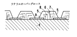
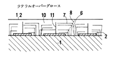
に記載されている。図14〜図17にその工程を示す。
【0024】
図14はサファイア基板の上にGaNを付けGaNの[11−20]方向に延びるストライプ窓マスクを設けた状態を示す。図15のように気相成長が始まるとマスク窓から優先的に選択成長がおこり(11−22)面、(−1−122)面が優先的に成長する。だから三角形のGaNの畝が窓にそって形成される。基板からの転位がGaN薄膜に引き継がれる。細線によって転位の方向を示す。上向きに成長しているから転位も上向きに進む。
【0025】
窓が埋まったのち、図16のようにGaNはマスク窓からはみ出して横方向に延びて行く。この間高さには大きな変化は見られない。最先端はファセット面(11−22)、(−1−122)である。これが横方向に成長してゆく。細線で示す転位は横方向に曲がる。
【0026】
やがて隣接マスク窓からの成長層がマスク窓中間で合体してファセット面が埋め込まれる。隣接窓の中間で転位が集合した面欠陥ができる。図17に示す。その後c面(0001)において、二次元的な成長が行われ鏡面状の成長が進行する。もちろん鏡面状の成長を行わせるのは容易でないが平坦平滑なGaN単結晶を作るのが目的であるから成長の途上でも鏡面を維持しつつ成長させなければならないと考えられている。
【0027】
この場合、窓から横方向にはみ出してマスクの上に成長した部分において、貫通転位密度が小さいことが既に報告されている。前記▲5▼はその原因を詳しく考察している。▲5▼の述べるマスクによる転位低減の理由は次のようである。結晶がc軸方向に成長する場合、転位もc軸方向へ延びてゆく。c軸方向に連続する転位が貫通転位である。ところがマスクの上を横方向(c軸と直角方向)に結晶が成長すると、大体の傾向として転位も横方向に延びる。だからc軸に直交する貫通転位が減少するのであろうと考えられる。
【0028】
先述の報告例▲5▼では、マスク窓の中で基板に対し垂直に成長した後、横方向に成長し始めるということが述べられている。またマスク上で隣接窓から成長した結晶が合体した部分に面状の欠陥部が形成されるということも述べられている。この面状の欠陥は膜厚が増えるとともに小さくなり、膜厚が140μm程度以上になると消失するということも▲4▼に報告されている。だから窓付きマスクを使ったラテラルオーバーグロースによってGaNのEPDを一挙に107cm−2のオーダーにまで減少させることができた、と述べている。
【0029】
本発明者も、この様なGaNのラテラル成長を行い、成長の詳細な様子を観察し検討した。以降の記述において、通常のエピタキシャル成長で見られる(0001)面すなわちc面での二次元成長と区別するためc面以外のファセット面を単にファセット面と呼ぶことにする。
【0030】
マスク上に延びた結晶は、膜厚が6μm程度の時に合体する。その後結晶は上方(c軸方向)に成長する。c面を積み重ねるような二次元的な成長であり平面を維持しながら成長した。表面は鏡面状の平面である。成長膜厚を0.2mmから0.6mmまで変化させてさまざまのGaN膜を成長させた。結晶中の転位密度は幾分低下したが、転位密度が1×107cm−2を下回ることはなかった。これでは半導体レ−ザのための基板としてはなお不十分であると言わねばならない。
【0031】
本発明者は、転位が減らない原因について次のように考えた。上向きの単純な二次元的な成長(平坦性を維持しながらc面を重ねてゆく、つまり鏡面成長)を行う限りでは、c面に垂直な方向に転位が延び続けるのみである。上向きに自由に延びるかぎり転位を消滅させるような機構が働かない。だから上向きに厳密に平坦性を維持しながら二次元的成長を行うかぎり一旦発生した転位を消去することができない。
【0032】
それに▲4▼、▲5▼などで行われている鏡面成長(全表面においてc軸方向に等速度で成長させること)はもう一つ問題がある。鏡面成長は成長温度が高すぎて、GaAsを基板にする場合高熱のためGaAs基板がぼろぼろに劣化してしまうという難点があった。サファイアを基板にする限り成長温度が高すぎるのは別段問題でないが、GaAsを基板としようとすると成長温度をもっと下げる必要がある。本発明者はGaAs基板を用いたい。サファイアより化学的に反応しやすいからGaN成長後簡単にGaAs基板を除去できる。こういう伏線もあった。
【0033】
さて、転位の問題に戻る。転位密度を低減するには、一旦発生した転位を消去するような何らかの機構がなければならない。単純に上方に一様速度で鏡面成長するのでは転位が減少しない。
【0034】
本発明者は、転位の消滅機構を結晶中にもうけ、これを保持したまま結晶成長を行うことによって転位低減が可能になるだろうと考える。
【0035】
転位消滅機構を発生させ、これを内在させたまま結晶成長を行うことのできる方法について検討した。そして転位を消去する機構を含む結晶成長法を見い出した。それが本発明である。
【0036】
本発明は平坦面を発生させるのではなくファセット面を生ずるような条件で結晶成長を行い、ファセット面を埋め込むような工夫をせず、最後までファセットが残るようにする。ファセット面が転位を消滅させるのである。
【0037】
本発明はファセット面に転位消滅機能があるということに初めて気づきファセット面によって転位を減少させるものである。隣接ファセット面は境界を持つがファセット面の境界に転位を集合させ消去する。ファセット面の境界は転位の集合面となるし、転位集合面の交線は転位が集積した多重線となる。ファセット面を利用して転位を減少させると、従来よりも1桁低い106cm−2以下の低転位のものを得ることができる。さらに驚くべきことに104cm−2〜5×103cm−2のような低転位のGaN単結晶をも作製できる。
【0038】
ここで述べるファセット面というのはc面でなく成長方向と直交しない面である。通常の結晶成長では平坦面を維持しながら成長させるようにする。だからファセットが発生するような成長はよくないのである。ところが本発明はその常識を反転させファセットの発生を許容しファセットが結晶成長中に連続して存在するようにして転位を低減するようにする。こうしてこれまで例を見ない低転位のGaN結晶を成長させることができた。これから低転位GaN基板を製造する事が可能になる。青色、紫色半導体レ−ザ用の基板として最適の結晶基板である。
【0039】
本発明のGaN成長様式は、次のように記述することができる。
(1)ファセット面を発生させファセット面を消滅させる事なく成長の最後までファセット面を存在させた状態で成長させること。
(2)ファセット面は隣接ファセット面との間に境界を有すること。
(3)複数のファセット面の交点である多重点を有すること。
これによって106cm−2以下の低転位GaN結晶を初めて実現できた。
【0040】
分かりにくい着想であるから詳しく説明する必要がある。ファセット面というのは成長方向に垂直な面(成長面)以外の面をいう。ここではc軸方向に成長させるからc面が成長面である。c面以外はファセット面ということになる。以後面や方向を具体的に述べるから、その定義をここできっちりと説明しておこう。
【0041】
GaNは六方晶系(hexagonal)であるから軸方向や面方位を表すには4つの指数を使う表記方法を採用する。3指数の表記もあるが、ここでは一貫して4指数の表現を用いる。a軸、b軸は120度をなし長さは等しい(a=b)これらに直交するc軸は特異な軸でありa軸と等しくない(c≠a)。a軸とb軸だけではab面の方向を表すさいに対称性がなくなるのでもう一つの軸を想定する。これを仮にd軸とする。a、bだけで充分に方位を指定できるが対称性を損なわないようにもう一つ余分の軸dを導入したのであるからこれらは互いに独立でない。一つの平行面群を4つの指数(klmn)で表現したとすると、これは原点から数えて1枚目の面がa軸、b軸、d軸、c軸を切る点の原点からの距離がa/k、b/l、d/m、c/nであるということである。これは他の晶系の場合と同じ定義である。ただしa、b、d軸は平面内に含まれる冗長な座標であるから、k、l、mは独立でなく、常にk+l+m=0というサムルールがある。c軸に関しては立方晶等の場合と同じである。同等な平行面がc軸単位長さにn枚あるときc方向の指数がnとなる。だから4つの指数のうち前3つについては回転対称性があるが、後ろひとつ(c軸)の指数は独立である。
【0042】
個々の面方位は丸い括弧(…)で表現する。集合的な面方位は波括弧{…}によって表現する。集合的なというのはある面方位をその晶系が許す全ての対称操作によって到達できる全ての面方位の集合を意味する。結晶方位も同じ指数によって表現する。結晶方位はそれに垂直な面の指数と同じ指数をつかう。個別の方位は角括弧[…]であらわす。集合方位は鍵括弧<…>で表現する。これらの事は結晶学の常識であるが混乱を避けるため説明した。マイナスの指数は数字の上に横線を引いて示すのが直観的に分かりやすくて結晶学の決まりでもある。しかし数字の上に横線を引く事ができないから、ここでは数字の前に−をつけて負数を示す。
【0043】
c軸方向に成長させるということは6方向に同等な軸をもつような面に成長させるということである。ファセット面はc面(0001)以外だということであるから、k、l、mのいずれかが0でなければファセット面だということである。
しかしそうはいっても対称性などから現れ易いファセットと現れにくい、或いは現れないファセットの別がある。出現頻度の高い主なファセット面は
【0044】
{1−212}、{1−211}、{n−2nnk}(n、kは整数)、{1−101}、{1−102}、{n−n0k}(n、kは整数)
【0045】
などである。先述のように{…}は集合的面の表示である。例えば{1−212}面は、個別面にすると(1−212)、(2−1−12)、(11−22)、(−12−12)、(−2112)、(−1−122)の6つの面を含む。この6つの傾斜面(ファセット面)が以後に述べる逆六角錐形状のピットを形成する面となる。しかし煩雑であるから6つの面の個別面指数は書かない。単に{1−212}のファセット面というように述べるが、実は上の6つの同等な面を差している。反対にもしも{2−1−12}、{11−22}などと表記していてもこれは{1−212}と全く同じ要素の集合で等価である。
【0046】
本発明において、転位低減の原因となる基本原理は、面方位の異なるファセット面とファセット面の境界に、或いは面方位の異なる複数のファセット面の集まる多重点に転位などの欠陥を寄せ集めるメカニズムが働いているためであると考えられる。
【0047】
それによって結晶内の転位等の欠陥がファセット面の境界面、ファセット面の多重点に集められた結果、結晶内の転位欠陥は、順次減少してゆき高品質化が進む。それと同時に欠陥の集合部となるファセット面の境界面、ファセット面の多重点には欠陥が増加してゆくことになる。本発明のあらましの原理は以上のようである。以下に本発明の原理をさらに詳しく説明する。ファセット面がどうして転位を寄せ集める作用があるのかということは分かりにくい。初めに2つのファセット面での転位の進行方向の曲がりについてのべ、ついで具体的な成長ピットでの転位の集積について説明する。
【0048】
一般に転位の進行する向きは、結晶成長の方向に依存する。GaN結晶の場合、マスク窓内のc軸方向の2次元的成長をしているとき転位はc軸方向に進む。マスクの縁を越えると結晶成長がらマスク上への横方向の成長モードに変わる。成長方向が横方向になると転位の進行方向も横方向に変わる。これはラテラルオーバーグロースに関する報告であきらかにされている。
【0049】
図14〜図17はラテラルオーバーグロースの工程を示している。これは先ほど説明したが転位を考えるためもう一度振り返る。図14は基板上にマスクをもうけた状態である。図15は基板の上にGaNを成長させた状態を示す。マスクで覆われない部分にGaNが(c軸方向に)成長する。マスク上には成長しないから三角畝状にGaN結晶ができる。転位は真っ直ぐ上向き(c軸方向)である。結晶外形の傾斜角は予め決まる。さらに成長が進むと図16に示すように結晶がマスクの上にのぼり横向きに(ab面内)成長する。転位は横方向に折れ曲がる。さらに成長が進むと隣接窓からのGaN結晶が被覆部の中点で相合してさらに上向きに成長する。相合線に大きい欠陥ができる。転位は相合線によって終端されて消滅するものもある。従来のラテラルオーバーグロースは相合以後平坦面(鏡面)になるように成長させていた。
【0050】
本発明は鏡面成長でなく、凹凸状のファセットを大量に含む成長を行わせる。すると異なるファセット面が交差する部分が多数現れる。ファセット面の交差部について考察する。これには二つの場合がある。
【0051】
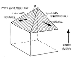
(1)ファセット面角度が180度以下の場合
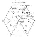
まず、異なる面指数のファセット面間のなす角度が180度より小さい場合、境界線が凸になっている場合を考える。図1にこれを示す。四角柱の上に傾斜面4つよりなる錐体を描いているが、これは一般の場合を書いている。二つのファセット面Fa、Fbだけを考えているのである。斜線を付けた斜面がファセット面である。平均的な成長方向はc軸方向である。
【0052】
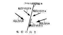
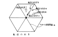
しかしファセット面での成長方向A、Bはファセット面Fa、Fbに立てた法線を底面に投影した方向である。転位が進行する方向は成長方向に等しいと考えられる。図2にファセット面状の成長方向と転位の進行方向を底面に投影したものを示す。成長方向Aと転位進行方向aは等しいが外側に発散する。ファセット面が凸に相合するから転位は外向きに進行する。ファセットの境界線mから転位は離れる。異なる転位線が交差することはない。この場合、自由に下地結晶を引き継いで結晶成長が進むものと考えられる。成長面指数の違いによる不純物濃度の差は有り得るが、転位などの欠陥の挙動については下地結晶の欠陥を引き継ぐに留まる。だから特に転位減少というようなことは起こらない。図3は成長後の状態を示す。厚みがますだけで転位密度は変わらない。ファセット交差角が180度以下(劣角)なら転位減少効果がない。
【0053】
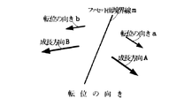
(2)ファセット面角度が180度以上の場合
重要なのは、異なる面指数のファセット面のなす角度が180度より大きい場合つまり境界線が凹になっている場合である。図4にこのような場合を示す。斜線部がファセット面Fa、Fbである。平均的な成長方向はc軸方向である。ファセット面での成長方向A、Bはファセット面に立てた法線を底面に投影した方向である。転位が進行する方向は成長方向に等しいと考えられる。図5にファセット面状の成長方向と転位の進行方向を底面に投影したものを示す。成長方向Aと転位進行方向aは等しいがこれらは内側に収束する。ファセット面が凹に相合するから転位は内向きに進行する。隣接ファセット面上の異なる転位線が境界線mで交差する。境界線で転位の向きcというように屈折する。図6のように転位線cは境界線に垂直な面内に集積される。
【0054】
結晶成長とともに集積線mは次第に上昇するから転位集積線mの軌跡は面になる。これが面状欠陥部Kである。面状欠陥部Kは小傾角粒界となりうる。面状欠陥部Kは二つのファセット面Fa、Fbの二等分面となる。ファセット面の上に存在した転位はこのように面に吸収されてファセット面から消えてゆく。面状欠陥部Kに集まった転位線はなお斜め内向きに進むから次第に中心線上に溜まってゆく。だから面からも転位が減少し中心線にたまってゆくことになる。これが本発明の転位低減の基本的な原理である。ファセット面の交差角度が180度以上(優角)であれば必ずこのような転位減少効果がある。
【0055】
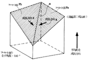
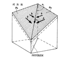
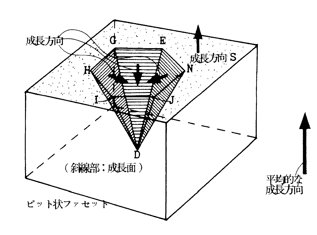
次に、面指数の異なる複数のファセット面が多重点を有している場合について述べる。図4〜図6と同じようなものであるが、図7はより具体的なファセット面の集合(ピット)を描いている。実際にファセットが出現するGaN成長をしてみると図1〜3のような突起にはならない。図4〜6のような凹部(ピット)になる。本発明はファセット面のこのような非対称性を巧みに利用しようとする。
図7は{1−212}面のなす逆六角錐EGHIJN−Dに該当する。図8はピットのc面への投影図である。平均的な成長方向はc軸方向である。ピット内では成長方向A、B…はその面に直角な方向、あるいは表面に平行でファセット面の横方向線に対し直交する方向であろうと考えられる。平坦な表面での成長方向はc軸方向である。ファセット面の成長方向A、B…に沿って転位線は延びて行く。Faでの転位の進行方向aはAと平行である。Fbでの転位の進行方向bはBと平行である。6つの角錐面(ファセット面)は同一速度で成長するから転位はやがて境界線mに至る。
【0056】
境界線mを越えて隣接ファセット面に転位が延びるか?という問題であるが、あるファセット面の成長方向Bと転位進行方向bは平行であった。隣接ファセット面の成長方向はそのファセット面の成長方向と60度異なる。もしも隣接ファセット面状の転位となるにはその転位は60度も方向を曲げる必要がある。これはできない。つまり転位は境界線mを乗り越えることができない。だから境界線mで消滅するか境界線mにそって中心へ向かうことになる。境界線mは結晶の特異線であるから転位が潜り込むのを許す。
【0057】
実際には平均的に上に向かう成長がおこっているのであるから、ピットは少しずつ埋まってゆく。にもかかわらずピットが小さくならないのは上方の開口部が広がろうとするからである。表面でのc軸方向の成長を速度をVとし、ファセット面の表面に対する傾きをθとして、ファセット面での成長速度がVsinθであるとするとピットの大きさは不変で上方へVの速度で上昇するだけである。古い転位は成長とともに結晶の中に埋まってしまう。つまり転位線は境界線mの中に埋め込まれる。転位が境界線mに入り込むので他の領域での転位は減少して行く。
【0058】
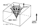
転位は隣接ファセット面の二等分面の中に埋め込まれる。この面を面状欠陥部Kとよぶ。図9にこれを示す。面状欠陥部Kはピット中心線に関し回転対称で互いに60゜の角度をなす面である。
【0059】
成長は上方向に起こるから、境界線にある転位は中心方向に推移する。だから転位の集合は境界線mを滑り落ちて中心軸線に溜まる。これが図9の多重点Dの下方の連続する線状欠陥部Lである。
【0060】
多重点Dには、他のファセット面境界からの転位、小傾角粒界などが合流し全てが集まってくる。こうして6つのファセット面が形成するピット内の全ての転位が多重点Dに集められるということになる。転位のいくらかはその推移の途中で消滅する。残りは凝集して多重点Dに残存する。
【0061】
多重点に集合した転位などの欠陥は成長とともに多重点の垂直下方に線状の転位欠陥の集合として残る。線状欠陥部Lである。その他に、ファセット面境界の下に帯状の欠陥(面状欠陥)Kも残るし、小傾角粒界も残存する。
【0062】
転位を集めた帯状の面欠陥、小傾角粒界、線状欠陥は確かに結晶中に残存する。
だから転位が減っていないと言えない。転位の多くは境界線に相合したとき消滅する。境界線から多重点に集合したときにも消滅する。さらに非常に狭い領域に集められた転位は、相互作用によって消滅する。例えば刃状転位同士の衝突により消滅する。だから成長とともに欠陥密度が減少して行くのである。
【0063】
面状欠陥、線状欠陥など欠陥の集合体の形成は成長条件とも関係しており、成長条件の最適化によって集合体を減らすことができる。成長条件によっては小傾角粒界などの面欠陥は消えてしまう場合もある。この場合の結晶性は良好である。
【0064】
また成長条件によっては、帯面状の面欠陥、小傾角粒界、線状欠陥の集合体の付近に多数の転位が集まって観察されることもある。線状欠陥などはエッチピットとしては一つと数えられる。簡単に言えば一つの多重点Dが平均例えば104個の転位を集めるとすれば、エッチピットは10−4に減るということになる。
【0065】
これまで本発明の転位低減方法を詳しく述べてきた。しかしまだ触れていない重大な問題点がある。これまで述べた方法はあくまでその時点でファセット部が存在する部位における転位低減法であった。結晶の一部でもc軸成長の部分(鏡面成長)があると、この部分では転位減少の効果が全くないということになってしまう。c軸成長の場合転位はc軸方向に運ばれるだけで減少することはないからである。
【0066】
図11に結晶の縦断面を示す。斜線部sがc軸成長部、白地部wがファセット成長部とする。図11は成長方向にこれらの断面が不変だという場合である。c軸成長部sと、ファセット成長部wの境界をqとする。境界qは成長方向に不変である。白地部分wでは先述の転位低減効果がある。しかし斜線部sでは転位は減少しない。初めのEPDをQとすると、これが斜線部では保存されるから、ファセット成長部でのEPDがたとえ0だとしても、最終的なEPDは比例配分になるから、EPD=Qs/(s+w)というふうになる。低減効果はs/(s+w)で与えられる。これはせいぜい1/2とか1/3程度にしかならない。ところが本発明は実施例で述べるように1/10000程度の減少効果をもたらすものである。
【0067】
この点に関しても、本発明者は既に巧みな解決策を準備している。その解決策について述べよう。
【0068】
GaN結晶の成長において、ファセットのできかたは、成長条件に依存する。例えば、NH3分圧、GaN成長速度、成長温度、ガスの流し方などの成長条件による。これらの成長条件を巧みに制御して鏡面成長がおこらずファセット成長が起こるようにする。従来の方法とは反対に本発明は鏡面を回避しファセットを選好する。
【0069】
例えば成長温度が高いほど鏡面になりやすく(c面成長)ファセットが生じ難い。成長温度が低いほどファセット成長しやすいということである。成長速度が遅いほど鏡面成長しやすくファセットが生じにくい。成長速度を上げるとファセット成長しやすいということである。NH3分圧が低いと鏡面になりやすい。つまりNH3分圧を上げることによりファセット成長させうるということである。HCl分圧が低い程鏡面になりやすい。だからHCl分圧を上げるとファセット成長しやすいということになる。つまり鏡面成長の反対の条件にするとファセット成長することができる。
【0070】
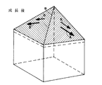
GaN結晶の成長中に、これらの成長条件を変動させて、ファセット面の存在する領域を横方向に変化させ、どの領域も厚さ方向に見てファセット成長をした経験があるようにする。ファセット成長した経験というのを単に「ファセット成長履歴」とよぶ。条件を時間的に変動させ、全面積においてどこかでファセット成長の履歴があるようにする。ファセット成長した部分は転位の種がなくなるから以後鏡面成長しても転位は存在しない。こうすることによって全表面において低転位密度化を達成することができる。結晶断面上向きに高さzをとる。成長厚みは時間に比例するから高さzは時間tに比例する。時間tで論じると履歴という時間を含む表現になる。結晶中に三次元座標(x,y,z)をとりファセット特性関数w(x,y,z)を定義する。これは(x,y,z)がファセット成長部分なら1、そうでない場合は0という値をとるような特性関数である。
w(x,y,z)=0 点(x,y,z)が鏡面成長
w(x,y,z)=1 点(x,y,z)がファセット成長
二次元の履歴特性関数W(x,y)は表面点(x,y)から垂線を下しz方向のどこかにファセット成長w(x,y,z)=1があれば、点(x,y)のWを1とし、z方向のどこにもファセット成長がなかったときは、点(x,y)のWを0とする関数であるとする。
W(x,y)=maxz{w(x,y,z)}
というように定義される履歴特性関数である。これが1ならz方向のどこかでファセット成長していたということである。表面全体でW(x,y)=1とすれば全面がファセット履歴を持つということである。しかし、たとえ表面全体でW(x,y)=1であったとしても任意のzに対するxy面で必ずw(x,y,z)=1となるというものでない。ある時刻(あるxy平面)でw(x,y,z)=1となる点が多いというような事情があれば表面全体でW(x,y)=1となる。
【0071】
図12はそのような場合の成長面の縦断面を示す。白地がファセット成長部(ピット成長部)wである。これは転位を吸収する作用があった。成長の初期に一時的にファセット成長領域(白地)の広い時がある。このときにファセット成長領域が転位を面状欠陥と線状欠陥に吸収してしまっている。その後その上の部分でc軸成長がおこっても転位の種がないので転位が存在しない。図12において斜線部(鏡面成長部)であってもその下方に白地(ファセット成長)が一旦存在しているなら転位はほとんどないのである。だから成長の終わりごろに斜線部(鏡面成長部)面積が大きくなっても低転位なのである。
【0072】
図13はいっそう極端にしたものである。成長の初期に全面においてファセット成長が起こるように(白地)している。ここでファセット成長が起こるので低転位化される。以後成長条件を変えてc軸成長(鏡面成長)させても転位の種がないから転位は伝達されない。このような横断的なファセット成長領域の動きによって全面において低転位化させることができる。
【0073】
軸方向にみてどこかでファセット成長の履歴があればその後c軸成長しても転位の数は少ない。であるから、ある時刻ある高さの面での転位分布はその高さでのファセット領域、鏡面領域の分布によっては決まらない。それまでの成長においてファセット成長があれば転位は下がっているのである。これまでファセット成長によって転位を線状欠陥に掃きよせるから転位が減るという説明をしてきたが、それならファセット面積Fと鏡面の面積(W−F)に転位が比例配分されるだけのように見える。それなら転位の劇的な減少は起こるはずがない。本発明は転位を10−4〜10−3のオーダーで減少させるが、その原因は縦方向の全てのファセット成長履歴が有効に働くというところにある。
【0074】
このようなファセット成長の履歴を与えるのはなるべく成長初期の方が効果的である。特に長いインゴットを作製する場合などは、なるべく成長初期にファセット履歴附与の操作を行うほうが工業的に有利となる。ファセット履歴を与えるには成長温度を下げる、HCl分圧を上げる、NH3分圧を上げる、成長速度を上げるなどのいずれかの手段を取れば良い。またファセット成長履歴附与作用は、成長中において、結晶成長部近傍の条件変動によって自然になされる場合もある。
【0075】
こうして転位を減少させつつ本発明のGaN結晶成長が行われる。本発明のGaN結晶には、帯面状の面欠陥、小傾角粒界、線状の転位欠陥集合体などが存在する。が、それらが含まれる領域以外の領域は、転位が殆ど存在しない。無転位の領域となっている。最終的に基板として使用する場合、貫通転位密度は極めて少なくて結晶性は大きく改善されている。LDの基板としても充分に実用に耐える低転位GaN単結晶となっている。
【0076】
以上に説明してきた本発明のGaN結晶成長法の基本概念を以下に纏める。
(1)ファセット面とファセット面との境界部へ転位が移動することによる転位の低減。
(2)ファセット面境界下部に転位が集合することによる欠陥面(面状欠陥部)の形成。
(3)複数のファセット面の交差する多重点における転位の合流、閉じ込めによる転位の拡散防止。
(4)多重点下部に転位が集合することによる線状欠陥部の形成。
(5)ファセット面成長履歴保有領域の拡大による低欠陥部の増加。
【0077】
これらの作用によって、本発明は、多重点以外に殆ど転位欠陥が存在せず、多重点のみに転位欠陥を有するGaN単結晶を得る事ができる。多重点はEPDの観測で一つのエッチピットとして計算される。もしも一つの多重点(線状欠陥)が例えば平均して104個の転位を集積できるとすると、初めに108cm−2の転位があった場合、104cm−2のレベルに転位を減少させることができる。
【0078】
以上、本発明の基本的な部分を説明した。さらに本発明の詳細な説明を行う。本発明は、これまで述べてきたように、気相成長の成長表面が平面状態でなく、三次元的なファセット構造をもったまま、ファセット構造を埋め込まないで成長することによって、転位を低減する単結晶窒化ガリウムの結晶成長法である(請求項1)。つまり鏡面にならずファセット面になるような条件でGaNを成長させるということである。
【0079】
三次元的なファセット構造としては、ファセット面を有するすり鉢状ピットであるか、或いはファセット面を有するピットの複合体などを意味する(請求項2)。
【0080】
さらに本発明は、ファセット構造をもったまま、ファセット面の境界部で平均的な成長面に対してほぼ垂直に面状の欠陥を有しながら転位を低減する単結晶窒化ガリウムの結晶成長法である(請求項3)。
【0081】
あるいは本発明は、ファセット構造をもったまま、複数のファセット面の多重点で平均的な成長面に対してほぼ垂直に線状の欠陥の集合部を有しながら転位を低減する単結晶窒化ガリウムの結晶成長法であるということもできる(請求項4)。
【0082】
成長ピットとなる場合は、{11−22}面がその側面として最も多く出現する。だから6つの同等な{11−22}面に囲まれた逆六角錐状のピットとなることが多い。次いで{1−101}面も出現することがある。その場合は先述の{11−22}と{1−101}によって逆12角錐状のピットとなる。ファセット面は殆ど凹部(ピット)となり隆起(突起部)にはならないという事が分かった。ファセット面の主な物は{11−22}、{1−211}、{n−2nnk}(n、kは整数)、{1−101}、{1−102}、{n−n0k}(n、kは整数)等である。
【0083】
本発明は、さらにまた、ファセット構造を埋め込まないで結晶成長することにより三次元的なファセット構造からなるピットを形成し平均的な成長方向に対してはほぼ垂直に線状の欠陥の集合部を有して、転位を低減しGaN単結晶を成長させる結晶成長法である(請求項5)。ファセット構造が逆六角錐状のピットであった場合、これら線状の欠陥の集合部は、ピットの底に連続して存在する。
【0084】
本発明はまた三次元的なファセット構造からなるピットの、ファセット面の境界線の下部に帯面状の面欠陥が存在するよう結晶成長させて、転位を低減する単結晶窒化ガリウムの結晶成長法である(請求項6)。
【0085】
本発明はさらに、三次元的なファセット構造からなるピット構造が逆六角錐である場合ピットのファセット面境界線の下部に存在する帯面状の面欠陥が放射状に60゜の角度をもって存在するよう成長させることにより、転位を低減するGaN単結晶の結晶成長法である(請求項7)。
【0086】
本発明は、GaN結晶成長中に、ファセット面の存在する領域を横方向に変化させ、任意のどの領域においても成長方向(縦方向)にファセット面成長の履歴をもたせることにより、転位を低減させる単結晶窒化ガリウムの結晶成長法である(請求項8)。
【0087】
三次元的なファセット構造からなるピットのファセット面は{11−22}面である場合が最も多い。その場合、ピット部下部に平均的な成長面に対してほぼ垂直に存在する帯面状の面欠陥の面方位は{11−20}である(請求項10)。 その場合、帯面状面欠陥は小傾角粒界として存在することもある(請求項11)。
【0088】
ファセット面を維持しながら成長させることだけが重要で本発明にとってGaNの成長方向は任意である。特に平均的な成長方向がc軸方向であると転位低減の効果はより大きい(請求項9)。
【0089】
本発明の転位低減の効果を得るためには、気相成長中および成長後のGaN結晶表面において、結晶表面の総面積Wに対する、三次元的なファセット構造の表面凹凸部の面積Fの比率F/Wが10%以上であることが必要である(請求項15)。ここで三次元的ファセット構造というのはファセット面からなるピットとピットの複合体を含むものである。
【0090】
一層転位低減効果を得るためには、総面積Wに対するファセット面積Fの比率F/Wが40%以上であることが望ましい(請求項16)。転位低減のためには有る程度以上の面積を三次元的ファセット構造によって覆う必要があるからである。
【0091】
より効果的に転位を減少させるにはファセット面積比を80%以上にする事が好ましい(請求項17)。80%以上となると、成長ピットからなるファセット構造の場合は、成長ピットは互いに連結しあうようになる。
【0092】
さらに三次元的なファセット面を含む成長ピットとその複合体の全てが互いに連結し表面にc面部が存在しない(F/W=100%)場合、転位削減効果は最も著しい(請求項18)。
【0093】
以上に述べたものは成長表面に現れるものが明確な方位をもつファセット面である場合である。しかし明確な方位のファセット面を持たない成長ピットが表面を占有する場合でも同様な転位低減効果がある、ということを確認した。例えば丸みを帯びた逆六角錐状のピットが存在する場合である。ピット面が明確な方位をもつファセット面でなくてもファセット面と同様に転位を減少させることができる。丸みを帯びた曲面からなっていてもピット状(凹部)になっているから転位線は面の継ぎ目で相合し消滅するのである。
【0094】
本発明は、気相成長後の表面における成長ピット及び成長ピットの複合体が、ファセット面からずれた曲面を有する場合をも含む(請求項19)。同様に、気相成長後の表面における成長ピット及び成長ピットの複合体からなる表面凹凸部の総面積に対する比率が10%以上であり、かつ全ての面がファセット面からずれた曲面を含むファセット面で構成された場合をも含む(請求項20)。
【0095】
三次元的ファセット面を有するピット径或いはファセット面を有するピットの複合体であるところのピット径は10μmから1000μmである事が望ましい(請求項29)。ピット径はあまりに小さすぎると転位低減効果が小さい。ピット径があまりに大きすぎると研磨時のロスが大きくなり非経済的である。
【0096】
【発明の実施の形態】
以上において説明したものはGaNの成長法である。GaN基板とするにはさらに次のような工程が必要になる。気相成長において、表面が平面状態でなく三次元的なファセット構造をもたせて低転位のGaN単結晶を成長させる。
【0097】
このファセット構造をもって成長させた低転位GaN単結晶を機械的加工して平面性を与える。さらに表面を研磨して平坦平滑な表面を持った単結晶GaN基板を得る(請求項12)。
【0098】
平面性を与えるための機械加工は研削加工であることもある(請求項14)。或いは平面性を与えるための機械加工はスライス切断加工であっても良い(請求項13)。
【0099】
本発明の結晶成長方法は、気相成長による。GaNの気相成長法としては、 ○HVPE法(Hydride Vapor Phase Epitaxy)
○MOCVD法(有機金属化学蒸着法;Metallorganic Chemical Vapor Phase Deposition)
○MOC法(有機金属塩化物気相成長法;Metallorganic Chloride Vapor Phase Epitaxy)
○ 昇華法
などがある。本発明はこれらの方法の何れを用いても実施することができる。ここでは最も簡便で成長速度も速いと考えられるHVPE法による場合について説明する。
【0100】
HVPE法というのは、ホットウォール型の反応炉の上流部にGaボートをもうけ加熱したGa融液にHClガスを吹き込むようにし、反応炉の下流部に基板をもうけNH3を吹き込むようにしておき、加熱したGaメタル(融液)にHClを吹きこんんでGaClを合成し、下方へ送り、下方でNH3と反応させGaNを合成しGaNが基板に堆積するようにしたものである。
【0101】
GaN成長に用いる基板としては、サファイア、SiC、Si、スピネル(MgAl2O4)、NdGaO3、ZnO、MgO、SiO2、GaAs、GaP、GaN、AlNなどの単結晶基板が適する(請求項23)。マスクを介することなく直接にこれらの基板の上にGaNを成長させることができる。マスクを介することも有効である(後述)。これらは格子定数や熱膨張率の点でGaNの基板として好適なものである。
【0102】
c軸方向にGaN単結晶を成長させる場合は軸廻りに六回対称性あるいは三回対称性がある単結晶基板を用いる必要がある。つまり結晶系としては六方晶系(hexagonal symmetry)であるか立方晶系(cubic symmetry)である単結晶である。立方晶系の場合(111)面を使えば三回対称性がある。上記のものは生成する時の温度や圧力によって二つ以上の晶系をとるものもある。
【0103】
ここでは、上記物質で六方晶系、立方晶系のものを選ぶ。サファイア、SiC、SiO2、NdGaO3、ZnO、GaN、AlNなどは六方晶系の単結晶を用いることができる。Si、スピネル、MgO、GaAs、GaPなどは立方晶系の(111)面基板を用いることができる。これはGaNをc面で成長させるものであるが、c面以外を表面にする場合は基板の表面もこれとは違ってくる。GaNと基板の対称性を合わせる必要がある。
【0104】
GaN成長の為の基板は、表面に開口部を有した非晶質または多結晶物質のマスク層をもうけたサファイア、SiC、Si、スピネル(MgAl2O4)、NdGaO3、ZnO、MgO、SiO2、GaAs、GaP、GaN、AlNなどの単結晶基板を使用することも有用である(請求項25)。マスクの使用はGaN結晶の低転位化に寄与するところがある。
【0105】
マスクのもうけ方にも2種類の選択肢がありうる。一つは基板の上に直接にマスクを形成する手法である。この場合エピ層に先立ち窓の内部の基板露出面にGaNバッファ層を堆積する等の工夫が必要になる。もう一つは基板の上に予め薄くGaN層を形成しておいて、その上にマスクを形成する手法である。後者の方が成長がスムーズに進行し、より好ましい場合が多い。
【0106】
マスクは沢山の開口部(窓)を持たなくてはならない。開口部にのみGaN結晶が成長するからである。マスクの上ではGaNが成長を開始しない。マスクはラテラル成長(Lateral Overgrowth)を行うためのものである。
【0107】
マスク窓の形状にも幾つかの選択肢がある。
▲1▼ドット形状…円形、正方形など孤立した点が規則的に分布するもの。c面のGaNを成長させる場合は、隣接する3つの窓が正三角形の頂点をなすように配列するとよい。列の方向はある低次の結晶方位に平行にする。
▲2▼ストライプ形状…多数の平行帯状の被覆部と開口部を交互にもうけるもの。被覆部の幅、開口部の幅、或いはピッチがパラメータとなる。帯状被覆部、開口部はある低次の結晶方位に平行になるようにする。開口部、被覆部長さは基板の長さに等しい。
▲3▼有限長ストライプ形状…有限長の帯状開口部をもうけたもの。被覆部の幅、開口部の幅、ピッチ、方位の他に、開口部長さもパラメータとなる。
【0108】
これらの窓付きマスクを使用した成長は、マスク無しの成長に比べて、初期の段階から、欠陥を低減することができるという効果がある。
【0109】
マスク付き基板、あるいはマスクなし基板の上に、ファセット面を多数有するGaN結晶を気相成長させる。このあと、凹凸のある表面を研削加工によって、平坦平滑化する。
【0110】
下地基板と上方のGaN結晶の材料が異なる場合は、エッチング、研削加工によって下地基板を除去することもできる。下地基板を除去し基板側を研削研磨して裏面も平坦に加工することもできる。これは1枚のGaNウエハを作製する場合である。厚い結晶を成長させて、これを切断して複数枚のウエハを作製することもできる(請求項27、28)。
【0111】
そのため、サファイア、SiC、Si、スピネル(MgAl2O4)、NdGaO3、ZnO、MgO、SiO2、GaAs、GaP、GaN、AlNなどの単結晶基板の上に、GaNを複数枚分の厚さに気相成長してインゴットとした後、軸と直角の方向にスライス切断して複数枚のウエハを得るようにする(請求項24)。
【0112】
或いは、表面に開口部を有する非晶質又は多結晶からなるマスク層を有するサファイア、SiC、Si、スピネル(MgAl2O4)、NdGaO3、ZnO、MgO、SiO2、GaAs、GaP、GaN、AlNなどの単結晶基板の上に、GaNを複数枚分の厚さに気相成長してインゴットとした後、軸と直角の方向にスライス切断して複数枚のウエハを得るようにすることもできる(請求項26)。
【0113】
1枚のウエハを作るときと同様に、このマスク層は、上記の基板上に直接に形成しても良いし、上記基板上にGaNエピ成長層を形成したあと、マスク層を形成しても良い。一般には後者の方が、成長がスムーズに進行し、より好ましい場合が多い。
【0114】
異質の材料を基板とするので、熱膨張率などの相違から、基板側やGaN結晶側にクラックが発生しやすい。そういう意味からは、GaAs基板が最も有望ということになる。熱膨張率、格子定数がGaNに近いからである。しかしGaAsは高熱の成長雰囲気でNH3との反応による損傷を受け易い。時に平坦な鏡面のGaN結晶を成長させようとする場合高温に加熱するがGaAs基板は高温にすると一部が軟化して崩れてしまう。本発明が採用するファセット面を保持する成長は鏡面成長よりも温度が低くて良い。ファセット成長の温度に対してはGaAs基板はよく耐える。だから本発明はGaAs基板を好適に利用することができる。
【0115】
GaAs基板(111)面上にマスク層を形成し、その上に平面状態でなく三次元的なファセット構造をもったまま、特にファセット面からなるピット及びピットの複合体を有したまま、それらのファセット構造を埋め込まないで成長させることにより転位を低減し、その後、GaAs基板を除去した後、表面、裏面を研磨することにより、単結晶GaN単体基板を製造する事ができる(請求項29)。GaAs基板の除去は、王水などのウエットエッチングによって容易になされる。
【0116】
こうして得られた単結晶GaNの単体基板を種結晶として、さらにGaN結晶を成長させることができる。GaN単体基板を種結晶として、その上に成長表面が平面状態でなく、三次元的ファセット構造をもちファセット構造を保ったまま、特にファセット面からなるピット、及びピット複合体を有したまま、ファセット構造を埋め込まないで低転位のGaN結晶を複数枚分の厚さに成長させ、軸垂直方向にスライス加工して複数枚のウエハとし、研磨加工することによってGaN単体基板を量産することが可能である(請求項30)。
【0117】
こうして得られたGaN基板は、最後に研磨加工が行われるが、本発明の成長様式が反映されたGaN基板となる。気相成長の成長表面が平面状態でなく三次元的なファセット構造をもったままファセット構造を埋め込まないでGaN結晶を成長させることにより転位を低減する。集積された転位は線状の欠陥の集合部を有しており、その線状欠陥集合部の密度は105cm−2以下である(請求項21)。
【0118】
線状欠陥集合部の密度の測定方法として二つある。一つは、CL(カソードルミネセンス)により測定する方法である。試料側に負電圧を印加し電子ビームを試料に照射すると電子によって結晶内部の電子が励起される。これが元の状態に戻る時に光を発する。電子加速電圧を調節し価電子帯の電子が伝導帯に励起されて戻る時に発する光はバンド幅に等しいエネルギーを持つ。バンド端からの発光によるスキャン像を観察すると、ピット部は白い領域として観察され、c面を成長面として成長した領域は、黒い領域として観察される。これらの線状欠陥部は、ピット面成長部である白い領域の中の黒い点として観察される。だからCLにおいてある面積中の黒い点の数を数えて面積で割れば線状欠陥の密度が分かる。
【0119】
また、もう一つの測定方法は、エッチピット密度の測定である。線状欠陥は以下の手法によって大きなエッチピットとして観測される。250℃に加熱した硫酸、燐酸の混酸の中で、測定すべきGaN単結晶基板をエッチングし、その表面のピット数をカウントすることによって測定される。
【0120】
通常の転位はせいぜい数μm径のエッチピットとなるが、これらの線状欠陥部は10μmから数十μm径の大きな六角形エッチピットとして観察される。このような大きな六角形状のエッチピットの密度を観測すると、密度としては105cm−2以下として観測される。また、この欠陥の集合部の大きなエッチピット以外にも、通常の転位に起因する小さなエッチピットも観測され、それらの合計の密度は106cm−2以下である(請求項22)。
【0121】
【実施例】
[実施例1(サファイア上、マスク無し成長+研削加工)]
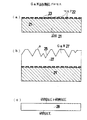
図18(a)〜(c)に実施例1の工程を示す。基板21の上に窓付きのマスク22を付ける。基板はサファイア、GaAsなど先述の基板の何れでも良い。窓を通してGaN結晶を気相成長させる。鏡面条件を避け、ファセット成長する条件で成長させるから図18(b)のようにファセット面25が無数に現れた凹凸に富む表面となる。鏡面sも幾分存在することもある。凹凸表面を研削加工および研磨加工して平坦平滑な表面とする。図18(c)のように基板つきのGaN単結晶を得る。
ここでは基板としてサファイア単結晶基板を使用した。c面の単結晶サファイア基板である。表面全体に予めHVPE法によって厚さ2μmのGaNエピ成長層を形成した。GaN/サファイア基板の2重構造の基板ができたことになる。その表面にストライプ状マスクを設けたもの(乙)と、マスクを設けずそのままのもの(甲)の二通りの基板を準備した。マスクストライプの方向(長手方向)はサファイア基板状のGaN層の<1−100>方向に平行になるようにした。マスク窓の幅は4μm、被覆部の幅は4μmで、周期8μmである。マスク材質はSiO2であり膜厚は0.1μmである。
【0122】
乙の基板はマスク/GaN/サファイアという三層構造を持ち、甲の基板はGaN/サファイアという二層構造をもつ。このような基板の上にHVPE法によって、GaN結晶の成長を行った。本実施例で用いたHVPE装置は、常圧の反応炉の内部にGaメタルを収容したボートを設けHCl+キャリヤガスをボートに向けて導入できるようにし、下方に基板を置き基板の近傍にNH3+キャリヤガスを引き込むようにしてある。周囲にはヒ−タがあってGaボートや基板を加熱できる。下方には排気口があり真空ポンプによって真空にひかれている。800℃に加熱されたGaボートに炉の上方からHClガスを流し、Gaメタルと反応させGaClを合成する。下方の基板の近傍にはNH3ガスを流しておき、下方へ落下してくるGaClと反応させ基板上にGaNを堆積させる。キャリヤガスはすべて水素とした。
【0123】
(バッファ層の形成)
まず基板を約490℃の低温に保持し、NH3ガス分圧を0.2atm(20kPa)、HCl分圧を2×10⁻³atm(0.2kPa)として、成長時間10分で、GaNバッファ層を約30nmの厚みに形成した。甲基板は100nm厚みのマスクがありマスクの上にはGaNが堆積しない。だから窓の内部にのみバッファ層が30nm積み上げられたことになる。乙基板は全面が30nmのバッファ層によって被覆される。
【0124】
(エピタキシャル層の形成)
これらの試料を980℃〜1050℃に昇温してバッファ層の上にさらにエピ層を設けた。甲基板(マスクなし)については二通りの条件でエピ層を形成した。これをサンプルA、Bとする。乙基板(マスクあり)については5種類の異なる条件でエピ成長した。これをサンプルC、D、E、F、Gとする。
【0125】
○サンプルA
使用基板 サファイア基板(マスクなし)
成長温度 1050℃
NH3分圧 0.2atm(20kPa)
HCl分圧 5×10⁻³atm(0.5kPa)
成長時間 8時間
成長層厚さ 290μm
【0126】
○サンプルB
使用基板 サファイア基板(マスクなし)
成長温度 1000℃
NH3分圧 0.3atm(30kPa)
HCl分圧 2×10⁻²atm(2kPa)
成長時間 3.5時間
成長層厚さ 420μm
【0127】
○サンプルC
使用基板 サファイア基板(マスクつき)
成長温度 1050℃
NH3分圧 0.2atm(20kPa)
HCl分圧 5×10⁻³atm(0.5kPa)
成長時間 9時間
成長層厚さ 270μm
【0128】
○サンプルD
使用基板 サファイア基板(マスクつき)
成長温度 1020℃
NH3分圧 0.2atm(20kPa)
HCl分圧 1×10⁻²atm(1kPa)
成長時間 6時間
成長層厚さ 330μm
【0129】
○サンプルE
使用基板 サファイア基板(マスクつき)
成長温度 1000℃
NH3分圧 0.3atm(30kPa)
HCl分圧 2×10⁻²atm(2kPa)
成長時間 3.5時間
成長層厚さ 400μm
【0130】
○サンプルF
使用基板 サファイア基板(マスクつき)
成長温度 1000℃
NH3分圧 0.4atm(40kPa)
HCl分圧 3×10⁻²atm(3kPa)
成長時間 3時間
成長層厚さ 465μm
【0131】
○サンプルG
使用基板 サファイア基板(マスクつき)
成長温度 980℃
NH3分圧 0.4atm(40kPa)
HCl分圧 4×10⁻²atm(4kPa)
成長時間 2.5時間
成長層厚さ 440μm
【0132】
これら6つのサンプルの成膜パラメータは以上のようである。サンプルAとCは同一の条件であるが時間が違う。サンプルBとEは同じ条件で時間も同じであるが膜厚が異なる。
【0133】
温度は重要なパラメータであるが、サンプルA、C、Dは1050℃、1020℃など比較的高い温度にして膜を作っている。サンプルB、E、F、Gは1000℃以下の比較的低温での成長となっている。
【0134】
NH3分圧も成膜に影響するように見える。サンプルA、C、DはNH3分圧が0.2atm(20kPa)である。サンプルB、EはNH3分圧が0.3atm(30kPa)である。サンプルF、Gは最も高くて0.4atm(40kPa)である。
【0135】
HCl分圧に関して言えば、サンプルA、C、Dは10−2atm(1kPa)以下であり、サンプルB、E、F、Gは2×10⁻²atm(2kPa)以上である。
【0136】
同じ条件が持続する限り時間と成長層厚さは比例するだろうと考えられる。単位時間当たりの成長速度はサンプルC(30μm/h)、A(36μm/h)が特に低い。サンプルD(55μm/h)も低い。これらは100μm/h未満の成長速度である。サンプルB(120μm/h)、E(114μm/h)、F(155μm/h)、G(176μm/h)はいずれも100μm/hを越えている。
【0137】
成長速度が大きいサンプル(G、F、B、E)は、概していえば、NH3分圧が高く、HCl分圧が高く、温度が低いものである。反対に、NH3分圧が低く、HCl分圧が低く、温度が高いと成長速度は遅い(C、A、D)ようである。
【0138】
これらサンプルの表面を顕微鏡観察した。成長表面の状態をサンプル毎に次に述べる。また成長表面の顕微鏡写真を画像解析し、ピット部の面積Fを表面全体の面積Wで割った値(ファセット部比率)F/Wを求めた。
【0139】
成長後の表面は、成長条件によって様々に異なる。あるものは鏡面成長しきれない平坦面となった。あるものはピット状ファセットによって覆われて著しく凹凸のある表面となった。鏡面成長したサンプルA、Cは表面はc面であり平滑平坦でファセットはまったく存在しない。殆ど鏡面状態のサンプルDは10%程度のファセット部を含む。
【0140】
それ以外のサンプルB、E、F、Gは三次元的ファセットがピットとして表面を覆っている。ピットにおけるファセット面は{11−22}面となっていることが多い。その場合ピットは逆六角錘形となる。{11−22}面と同時に{1−101}面が出る場合もある。その場合ピットは逆12角錘形となる。平坦部はc面となることが多い。しかしc面以外に低傾斜角の面も出現した。
【0141】
表面の顕微鏡観察のあと、各サンプルのGaN成長層の上から研削加工した。さらに表面を研磨してGaN結晶表面の平坦化を行った。研磨加工後の表面平坦性は、表面粗さがRmax1.5nm以下のレベルに仕上げ、製品形態(ウエハ)にした。
【0142】
その後いろいろな評価を行った。EPDを求めるため、硫酸、燐酸の混酸を250℃に加熱した液にサンプルを浸しエッチングをおこないエッチピットが表面にでるようにした。エッチングによって出現したエッチピットを顕微鏡を用いて数えた。先述のようにファセット部面積比率F/Wは顕微鏡写真の画像解析によって算出した。c面からわずかに傾いた低傾斜面は画像解析ではc面に含まれてしまう。だからF/Wの値は必ずしも定義に忠実でない。むしろピット部と総面積の比と考えるべきである。以下に成長後表面状態、ファセット面積比率F/W、EPDの測定値を各サンプルについて示す。
【0143】
○サンプルA
成長後の表面状態:鏡面状態で、表面ピットは観測されず。
成長後のファセット部面積比率(F/W): 0%
EPD: 1×108cm−2
【0144】
○サンプルB
成長後の表面状態:平面部とファセットが混在。ファセットは表面ピットとして数多く観測される。
成長後のファセット部面積比率(F/W): 約50%
EPD: 3×105cm−2
【0145】
○サンプルC
成長後の表面状態:鏡面状態で、表面ピットは観測されず。
成長後のファセット部面積比率(F/W): 0%
EPD: 3×107cm−2
【0146】
○サンプルD
成長後の表面状態:殆ど鏡面状態で、表面ピットはところどころに観測される。
成長後のファセット部面積比率(F/W): 10%
EPD: 8×105cm−2
【0147】
○サンプルE
成長後の表面状態:平面部とファセットが混在。ファセットは表面ピットとして数多く観測される。
成長後のファセット部面積比率(F/W): 約40%
EPD: 5×104cm−2
【0148】
○サンプルF
成長後の表面状態:鏡面状態からほど遠い。部分的にc面平面部が観察される。ピットが連結した状態。
成長後のファセット部面積比率(F/W): 約80%
EPD: 2×104cm−2
【0149】
○サンプルG
成長後の表面状態:全面にわたってピット叉はそれ以外のファセットからなる表面状態。
成長後のファセット部面積比率(F/W):ほぼ100%
EPD: 1×104cm−2
【0150】
これらのサンプルのうち、ファセットの存在しないサンプルA、Cは本発明に含まれない。サンプルB、D、E、F、Gにおいてはファセット成長しており本発明の構成となっている。いずれもEPDが極めて小さい。従来いかにしてもGaN結晶のEPDは107cm−2以下には下がらなかったが、これらサンプルはいずれも106cm−2より小さくなっている。本発明の目的はEPDを106cm−2以下に下げることであった。いずれの実施例もこれを満たす。サンプルD、Bは8×105cm−2、3×105cm−2であり要求を満たす。サンプルE、F、Gは104cm−2代であり、かつて類例をみない未曾有の低転位GaN単結晶である。
【0151】
サンプルA、Bはともにマスクを使用しないでGaNエピ層を形成したものである。これらを比較しよう。本発明のものでないサンプルAは成長温度が高くNH3、HCl分圧が低く成長速度が遅くて鏡面成長している。ところがEPDは高くて108cm−2もあり、従来レベル(107cm−2以上)である。
【0152】
本発明に属するサンプルBは成長温度低くNH3、HCl分圧が高く成長速度が速くてファセット成長している。ファセット比率は50%であり、EPDは3×105cm−2であるから課題(<106cm−2)を満たしている。何れもマスクなしなのであるからサンプルBにおいてEPDがサンプルAの1/300に減少した原因はマスクにない。
【0153】
EPD減少の原因がファセットの存在にあるのは明らかである。ファセットの存在するところがEPDが0になり、鏡面の部分は従来どおりというような単純なものでない。もしそうならEPDは鏡面部分の密度とファセット領域の密度によって比例配分されるはずである。ファセット部分がサンプルBにおいて50%であるから、もし単純な比例配分であれば、EPDは全体としてAの半分の5×107cm−2となる筈である。ところが1/300に減っている。ということはサンプルBにおいて鏡面になっている領域もEPDが減っているということなのである。だから鏡面領域の内奥部に何らかの変化が起こっているということである。
【0154】
サンプルA(マスク無し)とサンプルC(マスク有り)はいずれもファセットがなく完全な鏡面となっている。温度が高くNH3、HCl分圧が低く成長速度が遅いという共通の性質があった。両者を比較するとマスクの影響を知る事ができる。サンプルAは108cm−2、Cは3×107cm−2であるからいずれも従来技術の壁(>107cm−2)を越えない。EPDが、BはAの約3割に減少している。これはサンプルCがマスク窓を通した成長をしているからである。マスクの利益はEPDを3割程度に減少させるに過ぎない。ファセットの方がより劇的にEPDを減少させることができる。
【0155】
ファセットによる転位削減効果はサンプルDによっても良く分かる。サンプルDは殆どが鏡面であってピットの存在する面積は10%に過ぎない。にもかかわらずEPDは8×105cm−2に減少している。マスク有りの従来技術(サンプルC;3×107cm−2)と比較してもEPDが1/40に減少している。ファセット領域だけEPDが0で鏡面領域は従来と同じEPD密度だとすればファセット面が0.1ならEPDは2.7×107cm−2にしか低下しないはずである。表面におけるファセット面の比率は0.1なのであるが、ファセット履歴が鏡面におけるEPDをも減少させているのである。鏡面領域の内部にファセットが影響を及ぼしている。先述のように本発明のファセットによる転位減少は表面だけをみていては理解できない。
【0156】
サンプルE、F、GはいずれもEPDが104cm−2のオーダーで類例がないと書いた。その中でも最もEPDが小さいのはファセット面積比率が100%のサンプルG(1×104cm−2)である。3つの内でEPDが多いのはファセット比率が40%のサンプルE(5×104cm−2)である。これらのことから、ファセット領域がたとえ表面の10%程度でもEPD減少には卓抜した効果(サンプルD)があり、ファセット比率が高いほどEPDの低減は著しいという事が分かる。
【0157】
ピット状ファセット成長したサンプルの縦断面を、透過電子顕微鏡で観察した。何れのサンプルでも、ピット状ファセットの中心部に、基板面に垂直に筋状の欠陥が存在するという事が分かった。これはc軸方向の筋状欠陥である。
【0158】
またピットの中心部の筋状の欠陥を含んだ面状の欠陥も見られた。場合によっては、ピット中心の筋状欠陥を中心に約60゜の角度をもって放射状に開く面状欠陥を有することもある。これらの面状欠陥の面方位は{11−20}であった。面状欠陥は小傾角粒界となっていることが確認された。
【0159】
結晶の透過電子顕微鏡観察の結果は、サンプルB、D、E、F、Gともにほぼ同じ様な状況であった。ピット中心部では転位が見られたが、ピット中心から離れた箇所では透過電子顕微鏡の視野内では殆ど転位がみられない、という場合が多かった。
【0160】
この実施例でEPDを104cm−2のオーダーまで低減できた。さらなる条件の最適化によって、EPDをさらに低くできる可能性がある。また104cm−2の程度のEPDであれば、このGaN基板上にLD(レ−ザダイオード)を作製した場合、十分な長寿命が得られるであろうことが期待される。また、LD用基板としてさらに有用なものとするために、比較的厚さの厚いサンプルF、Gについては裏面のサファイアを研削により除去し、単体のGaN基板とする事ができた。
【0161】
[実施例2(GaAs基板上、厚付け+スライス加工)]
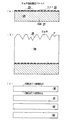
図19(a)〜(c)に実施例2の工程を示す。基板21の上に窓付きのマスク22を付ける。基板はサファイア、GaAsなど先述の基板の何れでも良い。窓を通してGaN結晶27を気相成長させる。鏡面条件を避け、ファセット成長する条件で成長させるから図19(b)のようにファセット面25が無数に現れた凹凸に富む表面となる。鏡面sも幾分存在することもある。基板を除去してGaN結晶27を取りだし凹凸表面を研削加工および研磨加工して平坦平滑な表面とする。図19(c)のようにGaN単体の単結晶28を得る。
実施例1はサファイアを基板としてGaNウエハ1枚だけを作製したものであった。今度は一つの結晶から複数枚のウエハを切り出す(スライス)ことができるようにする。結晶の上下の位置の違いによるEPDの相違を知るためである。またサファイア基板でなくGaAs基板を用いることにする。
【0162】
2インチ(111)GaAs基板のGa面((111)a面ともいう)を使用した。マスクにするため、GaAs基板の全面にSiO2膜をプラズマCVD法によって形成した。マスクの厚みは0.1μmである。その後フォトリソグラフィによってマスク窓を開けた。
【0163】
マスク窓は様々の形状が可能であるが、ここではドット状の窓を千鳥配列になるように設けた。ドット窓は直径2μm程度の大きさで円形でも正方形でも良い。GaAs基板の<11−2>方向に4μmピッチで1列に配列し、かつ<11−2>方向に3.5μm離れたところに同じ4μmピッチで同じ大きさのドット窓の列を設ける。隣接する列に属するドットは<11−2>方向に2μm(半ピッチ)ずれるようにした。これを<11−2>方向に繰り返す構造とした。つまり近接する3つのドット中心を結ぶと1辺が4μmの正三角形ができるような窓の配列である。
【0164】
ドット窓付きマスクを形成したGaAs基板に、HVPE法によってGaNバッファ層とエピ層を形成した。実施例1と同様に、常圧の反応炉の内部上方にGaメタルを収容したボートを設け800℃に加熱しHClガスを流してGaClを生成し、下方の基板付近に吹き込むNH3ガスとGaClを反応させて基板上にGaN膜を成長させる。実施例1はウエハ1枚分だけの成長であったが、実施例2は複数枚ウエハを製造しようとするものである。実施例2で使用するHVPE装置は長時間成長が可能な構造となっており、実施例1の装置とは異なる設備である。
【0165】
(バッファ層の形成)
GaAs基板を約500℃の低温に保ち、NH3分圧0.2atm(20kPa)、HCl分圧2×10⁻³atm(0.2kPa)として約30分間GaN膜を成長させた。マスク窓のGaAs露出部のみに約80nm厚みのバッファ層が堆積した。キャリヤガスはいずれも水素ガスである。
【0166】
(エピ層の形成)
GaAs基板の温度を約1000℃に上げて、NH3分圧0.4atm(40kPa)、HCl分圧3×10⁻²atm(3kPa)とした。成長時間は約100時間であった。
100時間のエピ成長によって、高さが25mmのGaNインゴットが作製できた。インゴットの底にはGaAs基板がついたままである。GaN成長表面は、二次元的な平面(鏡面)成長でなく、高密度のファセットが見られる。平面成長部であるc面からなる領域は10%程度しかない。90%がファセットの存在する領域である(F/W=0.9)。{11−22}面からなる逆六角錐状のピットも数多く観察された。
【0167】
このインゴットを、スライサーによりスライス切断加工して薄片(ウエハ)を得た。GaAs基板側の約2mm厚の部分と、成長面側の約3mm厚の部分は切り捨てた。薄片を研磨加工して、表面が平坦な2インチ径、厚さ350μmのGaN基板が20枚得られた。
【0168】
同一のGaNインゴットであっても部位によってEPDは違う。そこでGaAs基板側に近いウエハ(H)、中央部のウエハ(I)、成長面側に近いウエハ(J)の3枚を取り出して実施例1と同様の顕微鏡観察、画像処理によって表面状態、EPD等を調べた。
【0169】
○サンプルH EPD:8×103cm−2
○サンプルI EPD:6×103cm−2
○サンプルJ EPD:5×103cm−2
【0170】
このように極めて低いEPDの値が得られた。実施例1の場合最小EPDが104cm−2であったが、それよりなお低いのである。NH3分圧(0.4atm(40kPa))、HCl分圧(3×10⁻²atm(3kPa))ともに高く温度は低く(1000℃)て実施例1のサンプルFと同程度の成長条件である。
【0171】
研磨後のウエハの表面を観察すると、エッチピットは逆六角錐状で数μm〜数十μmのものまで様々のサイズのものがあった。カソードルミネセンスの実験から、エッチピットの中心は、結晶成長時のファセットからなる成長ピットの中心部に上下方向に合致することが多いということが分かった。特に径の大きいエッチピットはほとんどが結晶成長時の成長ピットの中心部に位置する。
【0172】
次に薄片に加工して試料を作製し透過電子顕微鏡によって縦方向の欠陥の観察をした。エッチピットの中心部でありファセットからなる結晶成長時の成長ピットの中心部に、基板面に垂直方向の筋状欠陥が見える。さらに筋状欠陥を含む面状の欠陥も観察される。場合によってはピット中心の筋状欠陥を含む面状の欠陥が60度の挟角をもって存在している。ピット中心部付近では複数の転位が見られた。しかしピット中心から離れた箇所では透過電子顕微鏡の視野内で殆ど転位が見られなかった。また、カソードルミネッセンスの結果から、エッチピットの外形が正六角形状からややずれて、丸みを帯びた曲線を持った形状となっている箇所もあったが、転位低減効果については同等であった。
【0173】
このような極端な低転位GaNはこれまで全く存在しなかった。このような低転位のGaN基板を使用してGaN系のLDを作製すると長寿命のレ−ザデバイスを作製できる可能性がある。
【0174】
[実施例3(サファイア基板、厚付け+スライス加工)]
図20(a)〜(c)に実施例3の工程を示す。基板21に上に窓付きのマスク22を付ける。基板はサファイア、GaAsなど先述の基板の何れでも良い。窓を通して厚みのあるGaN結晶29を気相成長させる。鏡面条件を避け、ファセット成長する条件で成長させるから図20(b)のようにファセット面25が無数に現れた凹凸に富む表面となる。鏡面sも幾分存在することもある。厚みのあるGaN結晶29を軸と垂直の方向に切断し複数枚のウエハとする。ウエハの表面を研削加工および研磨加工して平坦平滑な表面とする。図20(c)のように複数枚のGaN単体のミラーウエハ30、31、32、33…を得る。
実施例2はGaAs基板を使ってGaNを厚付けしスライスして20枚のウエハにした。今度はサファイア基板を使ってGaNを厚付けしスライスして複数枚のウエハを得るようにしよう。
厚さ0.4mmのc面を有するサファイア単結晶を基板とした。予めHVPE法で、サファイア表面に約1μmのGaNエピ層を形成した。
【0175】
その表面に0.1μm厚みのマスク材料(SiO2)を被覆した。マスク窓はさまざまの形状が可能であるが、実施例2と同様のドッド窓とした。寸法や周期は同様である。サファイアの上にGaN層があるからGaN層の方位に対してマスク窓の配列の方向を定義する。
【0176】
ドット窓は直径2μm程度の大きさで円形でも正方形でも良い。GaN層の<1−100>方向に4μmピッチで1列に配列し、かつ<11−20>方向に3.5μm離れたところに同じ4μmピッチで同じ大きさのドット窓の列を設ける。隣接する列に属するドットは<1−100>方向に2μm(半ピッチ)ずれるようにした。これを<11−20>方向に繰り返すようにした。つまり近接する3つのドット中心を結ぶと1辺が4μmの正三角形ができるような窓の配列である。
バッファ層の形成は行わず、マスクの上から直接にエピ層を成長させた。実施例2と同じ長時間成膜できるHVPE装置を用いた。
【0177】
(エピ層の形成)
マスク/GaN/サファイア基板からなる基板の温度を約1030℃に保ち、NH3分圧0.35atm(35kPa)、HCl分圧4×10−2atm(4kPa)とした。成長時間は約100時間であった。実施例2と時間は同じであるが、NH3分圧は少し低く、HCl分圧は少し高くしてある。
【0178】
エピタキシャル成長によって、高さ約3cmのGaNインゴットが作製できた。冷却時の熱応力のため、インゴットの底に付いているサファイア基板にクラックが入っていた。GaNインゴットにはクラックはなく使用可能な状態であった。GaN成長表面は、実施例2と同様でファセットが数多く見られた。平面成長部であるc面からなる領域は極狭くて30%程度であった。ファセット領域が70%であるから、ファセット領域比率F/Wは0.7である。
【0179】
{11ー22}面からなる逆六角錐状のピットも多数観察された。インゴットをスライス切断加工して24枚のウエハを得た。サファイア基板側の3mm厚の部分と成長面側の3mm厚の部分は切り捨てた。24枚のウエハは研磨加工して厚さ350μmの平坦平滑なGaNウエハとした。
【0180】
実施例2と同じように同一インゴットの異なる部位からとったウエハ3枚を比較した。サファイア基板側に近いサンプル(K)、中央部のサンプル(L)、成長面側に近いサンプル(M)の3枚を取り出し、顕微鏡観察によって表面状態、EPD等を調べた。
【0181】
○サンプルK EPD:2×104cm−2
○サンプルL EPD:1×104cm−2
○サンプルM EPD:8×103cm−2
【0182】
実施例2より高いが、それでも十分に低いEPDの値が得られた。実施例1の場合最小EPDが104cm−2であったが、それと同等である。実施例1の手法はウエハ1枚しか作れないが実施例3の厚付け法は一度で数十枚のGaNウエハを製造できる。NH3分圧(0.35atm(35kPa))、HCl分圧(4×10⁻²atm(4kPa))ともに高く温度(1030℃)もまた高いということが重要である。これによってファセットの多い成長を持続する。
【0183】
研磨後のウエハの表面を観察すると、エッチピットは逆六角錐状で数μm〜数十μmのものまで様々のサイズのものがあった。カソードルミネセンスの実験から、エッチピットの中心は、結晶成長時のファセットからなる成長ピットの中心部に上下方向に合致することが多いということが分かった。特に径の大きいエッチピットはほとんどが結晶成長時の成長ピットの中心部に位置する。これも実施例2と共通する。
【0184】
次に薄片に加工して試料を作製し透過電子顕微鏡によって縦方向の欠陥の観察をした。エッチピットの中心部でありファセットからなる結晶成長時の成長ピットの中心部に、基板面に垂直方向の筋状欠陥が見える。さらに筋状欠陥を含む面状の欠陥も観察される。場合によってはピット中心の筋状欠陥を含む面状の欠陥が60度の挟角をもって存在している。ピット中心部付近では複数の転位が見られた。しかしピット中心から離れた箇所では透過電子顕微鏡の視野内で殆ど転位が見られなかった。
【0185】
このような低転位GaNはこれまで全く存在しなかった。このような低転位のGaN基板を使用してGaN系のLDを作製すると長寿命のレ−ザデバイスを作製できる可能性がある。
【0186】
[実施例4(サファイア基板、4段階エピ、厚づけ+スライス加工)]
図20(a)〜(c)に実施例4の工程を示す。基板21に上に窓付きのマスク22を付ける。基板はサファイア、GaAsなど先述の基板の何れでも良い。窓を通して厚みのあるGaN結晶29を気相成長させる。鏡面条件を避け、ファセット成長する条件で成長させるから図20(b)のようにファセット面25が無数に現れた凹凸に富む表面となる。鏡面sも幾分存在することもある。厚みのあるGaN結晶29を軸と垂直の方向に切断し複数枚のウエハとする。ウエハの表面を研削加工および研磨加工して平坦平滑な表面とする。図20(c)のように複数枚のGaN単体のミラーウエハ30、31、32、33…を得る。
実施例3と同様の方法によって、サファイア基板上にGaN層、マスク層(ドット窓)を形成した基板を準備した。
バッファ層はつくらず、エピ層だけの条件を変えて4段階の成長によって作製した。実施例2で用いたのと同じように長時間成長できるHVPE装置を用いた。
【0187】
(GaNエピ層の形成)
第1段階(最初の2時間)
成長温度; 1030℃
NH3分圧; 0.12atm(12kPa)
HCl分圧; 2×10⁻²atm(2kPa)
第2段階(次の2時間)
成長温度; 1030℃
NH3分圧; 0.35atm(35kPa)
HCl分圧; 2×10⁻²atm(2kPa)
第3段階(続く2時間)
成長温度; 1030℃
NH3分圧; 0.12atm(12kPa)
HCl分圧; 2×10⁻²atm(2kPa)
第4段階(残りの95時間)
成長温度; 1030℃
NH3分圧; 0.35atm(35kPa)
HCl分圧; 4×10⁻²atm(4kPa)
【0188】
成長時間の合計は101時間である。成長温度は1030℃で一貫している。1〜3段階は初期の短い間(6時間)の変化であり、おもにNH3分圧を変えている。4段階の95時間の成長は実施例3と全く同じ条件である。
【0189】
エピ成長の結果、実施例3とほぼ同じように高さ約3cmのGaNインゴットが作製できた。外観も実施例3と同じであった。成長表面の状態も実施例3と近似していた。実施例4のインゴットを実施例3と同様な加工(スライス加工+研磨加工)によって、24枚の2インチ径、厚さ350μmのGaNウエハを得た。実施例3と同じようにサファイア基板側の3mm厚みの部分、成長面側の3mm厚さの部分は切り捨てた。
【0190】
GaN基板を評価するため、実施例3、2と同様に、サファイア基板側のサンプル(P)、中央部のサンプル(Q)、成長面側に近いサンプル(R)の3枚のウエハをとって表面観察、EPD測定を行った。
○サンプルP EPD:1×104cm−2
○サンプルQ EPD:8×103cm−2
○サンプルR EPD:6×103cm−2
【0191】
実施例2、3と同じように成長面側へ行くほどにEPDが下がるという傾向がある。EPDは実施例3の場合よりさらに低くなっている。
エッチピットは逆六角錐状で径が2μm程度の小さいものから数十μm程度のものまでさまざまのサイズのものがあった。
【0192】
実施例3と実施例4のエッチピットを詳細に比較検討した。カソードルミネッセンス(CL)の結果から、径の大きいエッチピットは、基板に垂直な線状の欠陥に起因していると考えられる。径の小さなエッチピットは通常の貫通転位によるものと考えられる。詳しくみると、実施例3と実施例4において、小さい径のエッチピットの密度に差が見られた。実施例4の方が小さいエッチピットの密度が低い。
【0193】
この原因を調べるために、実施例3、実施例4のインゴットのサファイア基板に近い側の3mm程の(切り捨てた部分)結晶を割り、高さ方向の断面をカソードルミネセンスによって分析した。実施例4の方が、成長の初期において、ピット形状が大きく変化しており、ファセット成長領域が厚さ方向で全面に渡って存在しているということが判明した。
【0195】
これは実施例4において初期の成長条件を複雑に変動させピット形状を変化させたことによる。成長初期のピット形状変化によるファセット成長部が横方向に多様な変化をすることによる。厚さ方向において全領域にわたってファセット成長の履歴を持つようになって実施例4の転位を著しく減少させたものである。
【0196】
[実施例5(GaAs上種結晶+インゴット)]
基板としてGaAs基板を使用する。GaAs基板は、2インチ径(111)基板のGa面を使用し、実施例2と同様に、まず全面にSiO2膜をプラズマCVDによって0.1μm厚になるよう形成し、その後フォトリソグラフィによってマスク窓を開けた。
【0197】
マスク窓は、様々な形状が可能であるが、ここではストライプ状の窓を形成した。ストライプ窓は、3μm幅、6μmピッチでストライプの方向はGaAs基板の<11−2>方向とした。このようなストライプ窓をマスクの全面に形成した。SiO2マスクの膜厚は当然0.1μmである。
マスクを形成した基板上に、HVPE法によって、GaNを成長させた。実施例5におけるHVPE法は、実施例2と同じ装置を使用した。
【0198】
(バッファ層の形成)
実施例2と同様にして、まず約500℃の低温にて、NH3ガス分圧を0.2atm(20kPa)、HClガス分圧を2×10⁻³atm(2kPa)とし、成長時間約30分で、GaNからなるバッファ層を約80nmを成長させた。マスク膜厚(100nm)の方がバッファ層より厚いから、この段階ではマスク開口部(窓)のGaAs基板表面にGaNバッファ層が成長する。マスクの上にはGaNが堆積しない。
【0199】
(エピ層の形成)
その後1000℃まで昇温して、この温度でGaNエピタキシャル層を成長させた。同じHVPE装置内であるが条件が違う。NH3分圧0.4atm(40kPa)、HCl分圧3×10⁻²atm(3kPa)とした。成長時間は約4時間であった。
その後GaAs基板を王水中でエッチング除去した。さらに図19に示したプロセスに従って研削加工によりGaN結晶を外形加工した。表面を研磨加工することによって、厚さ約0.4mmのGaN結晶を得た。
この結晶のエッチピット密度を測定したところ、EPDは2×104cm−2であった。充分に低いエッチピット密度であって、単体でGaN単結晶基板として使用可能である。
【0200】
(GaN種結晶からのエピ成長)
次にこの基板を種結晶として、図21のプロセスに従って、インゴット作製を試みた。同じHVPE法を用いた。成長条件は、NH3分圧0.4atm(40kPa)、HCl分圧3×10⁻²atm(3kPa)である。100時間の成長時間で約2.6cmの高さのGaNインゴットを得た。クラックの発生は全くなく理想的な状態であった。成長表面の状態は、二次元的な平面成長でなく、ファセットが数多く見られた。平面成長部であるc面からなる領域は、全表面積にうち5%程度しかなかった。95%はファセット部であった。{11−22}面よりなる逆六角錐形状のピットも数多く観察された。
【0201】
このインゴットをスライサーによりスライス切断加工をしウエハに切りだした。これはスライサーの切断模様があるのでウエハの両面を研磨した。それによって、2インチ径、厚さ350μmの表面が平坦なGaN基板が25枚得られた。GaAs基板側であった1mm厚ほどの部分と、成長面側の3mm厚さ程の部分は切り捨てた。収率はこれまでのなかで最も高く、GaAs基板からの砒素の混入もなかった。良質の単結晶を得易い方法であった。
【0202】
これらのGaN基板(ウエハ)について評価を行った。評価のため、切りだしたGaNウエハのうち、GaAs基板側のウエハサンプルをS、インゴット中央部付近のサンプルをT、インゴット上部のウエハサンプルをUとした。実施例1と同様の方法によってウエハ面のEPDを測定した。EPDの測定結果は以下のようであった。
【0203】
○ サンプルS EPD:7×103cm−2
○ サンプルT EPD:5×103cm−2
○ サンプルU EPD:3×103cm−2
【0204】
以上のように、これまでで最も低いEPDの値が得られた。エッチピットを顕微鏡観察した。エッチピットは六角錐状で数μmから数十μmのものまで見られた。エッチピットは、結晶成長時のファセットからなる成長ピットの中心部に位置する事が多い、ということがカソードルミネセンスによる観察によって分かった。特に、径の大きいエッチピットは、そのほとんどが、結晶成長時の成長ピットの中心部に位置する。
【0205】
ウエハを薄片に加工し試料を作製して、透過型電子顕微鏡による縦方向断面の観察を行った。その結果、エッチピットの中心であり、かつファセットからなる結晶成長時の成長ピットの中心部に、基板面に垂直方向の、筋状の欠陥が観察された。また、ピットの中心部の筋状の欠陥を含んだ面状の欠陥も見られた。場合によっては、中心のピット中心部の筋状の欠陥を中心に約60度の角度で開いた6枚の面状の欠陥を有する場合があった。ピット中心部付近では、複数の転位が見られたが、全般に転位は少なかった。中心から離れた箇所では、透過電子顕微鏡の視野内では転位が殆ど見られなかった。
【0206】
【発明の効果】
本発明の単結晶GaNの結晶成長法及びGaN単結晶基板の製造法により、従来得られなかった106cm−2以下の低転位のGaN単結晶が得られるようになった。これにより低転位GaN単結晶の工業的な生産が可能になる。低転位GaN単結晶基板を使用して、長寿命かつ高品質の青色、紫色の短波長の半導体レ−ザが製作可能になる。
【図面の簡単な説明】
【図1】 隣接するファセット面のなす角度が180度以下の場合ファセット面を含む角錐において結晶は発散する方向に成長することを示す斜視図。
【図2】隣接するファセット面のなす角度が180度以下の場合転位の進行方向が成長方向と平行であるから転位は境界線から遠ざかることを示す平面図。
【図3】 隣接するファセット面のなす角度が180度以下の場合ファセット面を含む角錐において結晶は発散する方向に成長し転位も発散し角錐が上方へそのまま嵩上げされて成長することを示す斜視図。
【図4】 隣接するファセット面のなす角度が180度以上の場合ファセット面を含む逆角錐において結晶は内側に収束する方向に成長することを示す斜視図。
【図5】 隣接するファセット面のなす角度が180度以上の場合転位の進行方向が成長方向と平行であるから転位は境界線に近づくことを示す平面図。
【図6】 隣接するファセット面のなす角度が180度以上の場合ファセット面を含む角錐において結晶は収束する方向に成長し転位も境界線に収束し逆角錐が上方へそのまま嵩上げされて成長することを示す斜視図。
【図7】 GaN気相成長において逆六角錐ピットが表面に出現した状態を表す斜視図。
【図8】 成長ピットにおける成長方向B、転位の進行方向bなどを表し、転位が境界線に衝突することを示す逆六角錐の平面図。
【図9】 GaN気相成長において逆六角錐ピットが表面に出現した場合、転位が内向きに進行し境界線に集積され境界線を成長方向に延ばした面状の欠陥部が生成することを示す斜視図。
【図10】 成長ピットの逆六角錐における成長方向B、転位の進行方向bなどを示す平面図。転位が境界線に衝突し境界線状を内向きに進行し中心点に集積するから中心が転位の多重点となることを示す逆六角錐の平面図。
【図11】 成長条件を一定に保ちほぼ一定のピット面形状で成長した場合の結晶の縦断面図。斜線部が鏡面成長(c軸成長)部sであり、白地部がファセット成長部wである。
【図12】 成長条件を変化させファセット成長部と鏡面成長部を横方向に変化させて大部分にファセット成長の履歴をもたせるようにした場合の結晶の縦断面図。斜線部が鏡面成長(c軸成長)部sであり、白地部がファセット成長部wである。
【図13】 成長条件を変化させファセット成長部と鏡面成長部を横方向に変化させてある時刻に全体にファセット成長の履歴をもたせるようにした場合の結晶の縦断面図。斜線部が鏡面成長(c軸成長)部sであり、白地部がファセット成長部wである。
【図14】 GaNのラテラルオーバーグロースにおいて、基板に窓付きマスクをもうけた状態の断面図。
【図15】 GaNのラテラルオーバーグロースにおいて、マスクの開口部にのみGaN結晶が三角畝状に成長した状態の断面図。
【図16】 GaNのラテラルオーバーグロースにおいて、マスクの開口部を越えてマスク上を横方向に延びてGaN結晶が台形畝状に成長した状態の断面図。
【図17】 GaNのラテラルオーバーグロースにおいて、隣接する開口部から成長した結晶が二等分線状で相合しファセット面が消滅して平坦面を維持しつつ上方に鏡面成長している状態の断面図。
【図18】 本発明の一つの実施例にかかるGaNの成長過程を示す断面図。図18(a)は基板に窓付きマスクを形成した状態の断面図。図18(b)は窓開口部を通して基板にGaN結晶がファセット成長した状態の断面図。図18(c)は結晶成長面を研削加工しさらに研磨加工して平滑平坦にして基板つきのGaNウエハとしたものの縦断面図。
【図19】 本発明の他の実施例にかかるGaNの成長過程を示す断面図。図19(a)は基板に窓付きマスクを形成した状態の断面図。図19(b)は窓開口部を通して基板にGaN結晶がファセット成長した状態の断面図。図19(c)は基板を除去しGaN結晶を取りだし凹凸ある結晶成長面を研削加工・研磨加工して平滑平坦にし裏面も研削加工して単体のGaNウエハとしたものの縦断面図。
【図20】 本発明の他の実施例にかかるGaNの成長過程を示す断面図。図20(a)は基板に窓付きマスクを形成した状態の断面図。図20(b)は窓開口部を通して基板に厚みのあるGaN結晶がファセット成長した状態の断面図。図20(c)は基板を除去し長いGaN結晶インゴットを切断して複数枚のアズカットウエハとしてウエハの両面を研削加工して平坦平滑なミラーウエハにしたものの縦断面図。
【図21】 本発明の他の実施例にかかるGaNの成長過程を示す断面図。図21(a)は基板に窓付きマスクを形成した状態の断面図。図21(b)は窓開口部を通して基板にGaN結晶がファセット成長した状態の断面図。図21(c)は基板を除去しGaN結晶インゴットを切断して1つのアズカットウエハとしウエハの両面を研削加工して平坦平滑にしたものの縦断面図。図21(d)はそれを種結晶としてさらに長いGaNインゴットをファセット成長させた状態の断面図。図19(e)は長いGaNインゴットを切断して複数枚のウエハとし両面を研削加工しミラーウエハとしたものの断面図。
【符号の説明】
1 基板
2 マスク
3 開口部(窓)
4 三角畝状に成長したGaN結晶
5 ファセット面
6 縦転位
7 横転位
8 転向ファセット面
9 ファセット面
10 GaN鏡面結晶
11 面状欠陥部
12 鏡面表面
21 基板
22 マスク
23 開口部(窓)
24 エピ成長GaN結晶
25 ファセット面
26 基板付きGaNウエハ
27 エピ成長GaN結晶
28 GaNウエハ
29 厚付けエピ成長GaN結晶
30〜33 スライスしたウエハ
34 エピ成長GaN結晶
35 GaN種結晶
36 エピ成長GaN結晶
37〜40 スライスしたGaNウエハ[0001]
[Industrial application fields]
The present invention relates to a GaN single crystal substrate used for light emitting devices such as light emitting diodes (LEDs) and lasers (LDs) made of a group 3-5 compound semiconductor, and a crystal growth method and manufacturing method thereof.
[0002]
[Prior art]
Light-emitting devices using Group 3-5 nitride semiconductors (GaN, GaInN) have already been put into practical use for blue LEDs and the like. Since a wide GaN substrate cannot be obtained, sapphire has been used exclusively as a substrate for nitride semiconductor light emitting devices. Sapphire (Al2O3) Has sixfold symmetry in the (0001) plane, and a GaN single crystal thin film grows on it. The GaN thin film and the GaInN thin film on sapphire have extremely many dislocations. However, it can still be used as a blue LED and has a long lifetime. Sapphire is both chemically and physically robust and heat resistant. It is a very hard and stable substrate material. Because of these advantages, a sapphire substrate is exclusively used as a substrate for a GaInN blue LED.
[0003]
However, the sapphire substrate has the following problems. The sapphire substrate has no cleavage plane. Moreover, it is an extremely hard material. When a large number of LED elements are manufactured on a wafer and divided into chips, it cannot be naturally divided on a cleavage plane like a normal semiconductor. The wafer can only be cut into chips by mechanical means (dicing). The dicing process increases costs. In the case of a semiconductor laser, it is not possible to create a reflective surface by further cleavage. Therefore, there was a problem in terms of quality. In addition, there is a drawback that the cost for manufacturing the reflecting surface is increased. Furthermore, sapphire is an insulating substrate.
[0004]
This also causes various problems. Since it is insulative, the bottom surface of the substrate cannot be used as an electrode as in a normal LED. Therefore, it is impossible to make electrodes on the upper and lower surfaces of the device. It is necessary to remove a part of the device by etching to expose the GaN lower layer and use this as an n-electrode. Wire bonding must be performed twice to connect the lead and the electrode. A current flows in the lateral direction in the semiconductor layer to which the lower electrode is attached, but a certain layer thickness must be provided to reduce the resistance. For this reason, the lower semiconductor layer becomes thick. In addition, since two electrodes are formed on the same surface, a large chip area is required. For this reason, GaN devices on sapphire substrates are expensive.
[0005]
In order to solve these sapphire substrate problems, it has been proposed to use a SiC substrate. The SiC single crystal has a cleavage plane and can be naturally cleaved from here. It should be possible to solve the problems of the dicing process and the resonator of the semiconductor laser. SiC is conductive and the lower electrode can be provided on the bottom surface of the SiC substrate. There is no space for the electrode and only one wire bonding is required. However, SiC is much more expensive than sapphire and is difficult to obtain and uneasy to supply. Further, there is a problem of crystallinity of a thin film such as GaN grown on the SiC substrate. Due to the high cost, the SiC substrate GaInN-based blue LED is hardly practically used even now.
[0006]
The problem of crystallinity is described. When a GaN crystal thin film is grown on a sapphire substrate or SiC substrate, many defects such as dislocations are introduced into the epitaxial layer due to a lattice constant mismatch between GaN and the substrate material. The problem is that the crystallinity is poor because of different materials and different lattice constants. Actually, the epitaxial layer (GaN, GaInN, etc.) of a sapphire substrate GaN-based LED device currently on the market is 109cm-2It is said that there are high density dislocations.
[0007]
Somewhat lower for SiC substrates, 10 for epitaxial layers.8cm-2It is said that there is a degree of dislocation.
[0008]
In the case of a semiconductor such as Si or GaAs, such a high density of dislocations does not make an effective device. For device fabrication, dislocation-free crystals for Si and low-dislocation crystals for GaAs are essential.
[0009]
Strangely, a GaN-based thin film functions normally as an LED even with such high-density dislocations. High-density dislocations have not hindered the practical application of GaN-based LEDs. Deterioration does not progress due to dislocation. In the case of a GaInN-based blue LED, high-density dislocation does not become a problem in terms of LED function.
[0010]
That's fine for LEDs, but the presence of such many defects is still a problem when used as an LD. In the case of an LD that flows a much higher density current than an LED, there is a concern that defects are triggered, the lattice structure is disturbed, and the defects proliferate. Although a GaInN blue semiconductor laser is manufactured using a sapphire substrate, there is still a problem in terms of life. 109cm-2Many dislocations may limit the lifetime of GaInN-based LDs.
[0011]
Taking these points into consideration, the present inventors consider that the most ideal substrate for a GaN semiconductor device is a GaN single crystal. If a GaN single crystal is used for the substrate, the problem of lattice constant mismatch is eliminated. Also, since GaN has a cleavage property, the process of cutting the wafer into chips is facilitated. It can be used as a resonator mirror surface in the case of a laser. Moreover, the GaN crystal is conductive, and the electrode arrangement is simplified. In this respect, a GaN single crystal is optimal as a substrate. The reason why the GaN single crystal was not used is that a large GaN single crystal having a practical size could not be produced so far.
[0012]
Even if the solid raw material is heated, it does not become a GaN melt but sublimes. Since a GaN melt cannot be used, the chocolate ski method starting from the melt cannot be used. It is said that there is an equilibrium between the liquid phase (melt) and the solid phase at ultra high pressure, but it is extremely difficult to produce a GaN single crystal with an ultra high pressure apparatus. Even if a GaN single crystal can be synthesized with an ultrahigh pressure apparatus, it is a small crystal and is not suitable as a substrate. To produce large crystals from equilibrium, a huge ultra-high pressure device is required, which is not commercially available.
[0013]
The present inventor examined technical problems and proposed a method for reducing crystal defect density by vapor-phase growth of GaN through a windowed mask. This is called the lateral overgrowth growth method or simply the lateral growth method.
[0014]
(1) Japanese Patent Application No. 9-298300
(2) Japanese Patent Application No. 10-9008
[0015]
Proposed the lateral growth method of the present inventor. This is a method of obtaining a GaN crystal by providing a mask having a striped window and a dot-shaped window on a GaAs substrate, vapor-depositing GaN on the mask and removing the GaAs substrate. This is a means to make one GaN substrate,
[0016]
(3) Japanese Patent Application No. 10-102546
[0017]
Proposed a method of using such a GaN substrate as a seed crystal, further growing laterally to produce a thick GaN ingot, and slicing the ingot to produce a plurality of GaN substrates. These novel methods of the present inventors made it possible for the first time to manufacture a GaN single crystal substrate on a commercial basis. Since GaN has a cleavage plane, the problem of cleavage can be overcome by using GaN as a substrate. Since there is an n-type GaN substrate, an LED can be made thereon and an n-electrode can be provided on the bottom of the n-type GaN substrate. Since it is not necessary to provide two electrodes on the same plane, the chip area can be saved. One wire is enough. Thus, this GaN substrate is useful as an LED substrate. When the LD substrate is used, it is convenient because the cleavage plane can be a resonator mirror. However, this GaN substrate still has problems and cannot be an LD substrate.
[0018]
[Problems to be solved by the invention]
In order to realize a blue and violet short wavelength laser diode, it has become clear that the greatest problem is to further reduce the defect density in the substrate. Since it is a laser diode used under severe conditions of high current density, it has been clarified that defects such as dislocations adversely affect the characteristics and life of the laser. In particular, it has been found that in order to extend the life of the laser, the GaN crystal needs to have a lower defect density.
[0019]
In the conventional method, the dislocation density (EPD) of the GaN crystal is 1 × 10 even when lateral growth is performed using a stripe-shaped mask.7cm-2It did not become the following. Although a laser can be manufactured with such a GaN crystal, the EPD of a GaN substrate is 1 × 10 5 to make a long-lived GaN-based laser.6cm-2The following is strongly desired. It is necessary to lower the EPD further than the currently reached level. Here, the long life means a life of 10,000 hours or more.
[0020]
1 × 106cm-2It is a first object of the present invention to provide the following low dislocation GaN crystal. It is a second object of the present invention to provide a method for producing such a low dislocation GaN single substrate.
[0021]
[Means for Solving the Problems]
In order to solve the above-mentioned problems, the present inventor has studied a crystal growth mode by vapor phase growth.
Here, we looked back on the lateral overgrowth method as a crystal growth method for reducing dislocations, which has been attempted in the past.
[0022]
When using a stripe mask or the like and performing lateral overgrowth of GaN,
[0023]
(4) IEICE Transactions vol. J81-C-II, no. 1, p58-64 (January 1998),
(5) Akira Sakai, Akira Sakurai “Reduction of dislocation density by lateral growth of GaN” Applied Physics Vol. 68, No. 7, p774-779 (1999)
It is described in. The process is shown in FIGS.
[0024]
FIG. 14 shows a state in which GaN is attached to a sapphire substrate and a stripe window mask extending in the [11-20] direction of GaN is provided. As shown in FIG. 15, when vapor phase growth starts, selective growth occurs preferentially from the mask window, and the (11-22) plane and the (-1-122) plane grow preferentially. So a triangular GaN ridge is formed along the window. Dislocations from the substrate are transferred to the GaN thin film. The direction of dislocation is indicated by a thin line. Since it is growing upward, dislocations also progress upward.
[0025]
After the window is filled, GaN protrudes from the mask window and extends laterally as shown in FIG. During this time, there is no significant change in height. The most advanced are the facet surfaces (11-22) and (-1-122). This grows laterally. Dislocations indicated by thin lines bend in the horizontal direction.
[0026]
Eventually, the growth layer from the adjacent mask window merges in the middle of the mask window to embed the facet surface. A surface defect in which dislocations gather in the middle of adjacent windows is formed. As shown in FIG. Thereafter, on the c-plane (0001), two-dimensional growth is performed, and specular growth proceeds. Of course, it is not easy to carry out mirror-like growth, but it is considered that the purpose is to produce a flat and smooth GaN single crystal, so that it must be grown while maintaining the mirror surface even during the growth.
[0027]
In this case, it has already been reported that the threading dislocation density is small in the portion protruding laterally from the window and growing on the mask. The above (5) examines the cause in detail. The reason for dislocation reduction by the mask described in (5) is as follows. When the crystal grows in the c-axis direction, dislocations also extend in the c-axis direction. Dislocations continuous in the c-axis direction are threading dislocations. However, when crystals grow on the mask in the lateral direction (perpendicular to the c-axis), dislocations also extend in the lateral direction as a general tendency. Therefore, it is considered that threading dislocations orthogonal to the c-axis will decrease.
[0028]
In the above-mentioned report example (5), it is described that the crystal grows perpendicularly to the substrate in the mask window and then begins to grow in the lateral direction. It is also described that a planar defect is formed in a portion where crystals grown from adjacent windows are combined on the mask. It has also been reported in (4) that this planar defect becomes smaller as the film thickness increases and disappears when the film thickness is about 140 μm or more. Therefore, the lateral overgrowth using a mask with a window makes 10 GaN EPDs at once.7cm-2It was said that it was able to reduce to the order of.
[0029]
The present inventor also carried out such lateral growth of GaN, and observed and examined the detailed state of the growth. In the following description, facet planes other than the c plane are simply referred to as facet planes in order to distinguish them from the two-dimensional growth on the (0001) plane, that is, the c plane, which is observed in normal epitaxial growth.
[0030]
The crystals extending on the mask are combined when the film thickness is about 6 μm. Thereafter, the crystal grows upward (c-axis direction). It was a two-dimensional growth in which c-planes were stacked, and it grew while maintaining a flat surface. The surface is a mirror-like plane. Various GaN films were grown by changing the growth film thickness from 0.2 mm to 0.6 mm. The dislocation density in the crystal decreased somewhat, but the dislocation density was 1 × 107cm-2Never fell below. It must be said that this is still insufficient as a substrate for a semiconductor laser.
[0031]
The present inventor considered the reason why dislocations did not decrease as follows. As long as simple upward two-dimensional growth (c-planes are superposed while maintaining flatness, that is, mirror growth), dislocations only continue to extend in a direction perpendicular to the c-plane. As long as it extends freely upward, a mechanism that eliminates dislocations does not work. Therefore, once the two-dimensional growth is performed while maintaining the flatness strictly upward, the dislocations once generated cannot be erased.
[0032]
In addition, the mirror growth performed in (4), (5), etc. (growing at the same speed in the c-axis direction on the entire surface) has another problem. In the mirror growth, the growth temperature is too high, and when GaAs is used as a substrate, there is a problem that the GaAs substrate deteriorates in a rough manner due to high heat. As long as sapphire is used as the substrate, the growth temperature is not too high, but if GaAs is used as the substrate, it is necessary to lower the growth temperature. The inventor wants to use a GaAs substrate. Since it reacts more chemically than sapphire, the GaAs substrate can be easily removed after GaN growth. There was such a hidden line.
[0033]
Now back to the problem of dislocations. In order to reduce the dislocation density, there must be some mechanism for erasing dislocations once generated. If the mirror surface is simply grown upward at a uniform rate, dislocations do not decrease.
[0034]
The present inventor believes that dislocation elimination can be reduced by providing a dislocation annihilation mechanism in the crystal and growing the crystal while maintaining this mechanism.
[0035]
We investigated a method that can generate a dislocation annihilation mechanism and allow crystal growth with the dislocation mechanism. And we found a crystal growth method including a mechanism to eliminate dislocations. That is the present invention.
[0036]
According to the present invention, crystal growth is performed under conditions that do not generate a flat surface but generate a facet surface, so that the facet remains until the end without devising embedding the facet surface. The facet plane eliminates the dislocation.
[0037]
The present invention first realizes that the facet surface has a dislocation annihilation function and reduces the dislocation by the facet surface. Adjacent facet surfaces have boundaries, but dislocations are gathered at the boundaries of the facet surfaces to eliminate them. The boundary of the facet plane becomes a dislocation aggregation plane, and the intersection line of the dislocation aggregation plane becomes a multiple line in which dislocations are accumulated. When dislocations are reduced using the facet plane, it is 10 orders of magnitude lower than before.6cm-2The following low dislocations can be obtained. More surprisingly, 104cm-2~ 5x103cm-2Such a low dislocation GaN single crystal can also be produced.
[0038]
The facet plane described here is not a c-plane but a plane that is not orthogonal to the growth direction. In normal crystal growth, growth is performed while maintaining a flat surface. Therefore, the growth that causes facets is not good. However, the present invention reverses the common sense and allows the generation of facets, so that the facets are continuously present during crystal growth to reduce dislocations. In this way, an unprecedented low dislocation GaN crystal could be grown. From this, it becomes possible to manufacture a low dislocation GaN substrate. It is an optimal crystal substrate as a substrate for blue and purple semiconductor lasers.
[0039]
The GaN growth mode of the present invention can be described as follows.
(1) Growing in a state in which the facet surface exists until the end of growth without generating the facet surface and eliminating the facet surface.
(2) The facet surface has a boundary between adjacent facet surfaces.
(3) To have multiple points that are intersections of a plurality of facet planes.
106cm-2The following low dislocation GaN crystals were realized for the first time.
[0040]
It is necessary to explain in detail because the idea is difficult to understand. A facet plane is a plane other than a plane (growth plane) perpendicular to the growth direction. Here, since the growth is in the c-axis direction, the c-plane is the growth plane. The surfaces other than the c-plane are facet surfaces. I will describe the plane and direction in detail, so I will explain the definition here.
[0041]
Since GaN is hexagonal, a notation using four indices is used to represent the axial direction and plane orientation. Although there is a notation of 3 indices, here, the expression of 4 indices is used consistently. The a-axis and b-axis are 120 degrees and have the same length (a = b). The c-axis orthogonal to these is a unique axis and is not equal to the a-axis (c ≠ a). Since only the a-axis and the b-axis have no symmetry in expressing the ab plane direction, another axis is assumed. Let this be the d-axis. Although it is possible to specify the azimuth sufficiently with only a and b, an extra axis d is introduced so as not to impair the symmetry, so they are not independent of each other. If one parallel plane group is expressed by four indices (klmn), this means that the distance from the origin at the point where the first plane is cut from the a-axis, b-axis, d-axis, and c-axis when counted from the origin. a / k, b / l, d / m, c / n. This is the same definition as in other crystal systems. However, since the a, b, and d axes are redundant coordinates included in the plane, k, l, and m are not independent, and there is always a sum rule that k + 1 + m = 0. The c-axis is the same as in the case of cubic crystals. When there are n equivalent parallel surfaces in the c-axis unit length, the index in the c direction is n. Therefore, the front three of the four indices have rotational symmetry, but the rear one (c-axis) is independent.
[0042]
Each plane orientation is expressed by round parentheses (...). The collective plane orientation is expressed by curly braces {...}. Collective means a set of all plane orientations that can be reached by all symmetry operations that the crystal system allows a plane orientation. The crystal orientation is also expressed by the same index. The crystal orientation uses the same index as the index of the plane perpendicular to it. Individual orientations are represented by square brackets [...]. The set direction is expressed in square brackets <...>. These things are common sense of crystallography, but explained to avoid confusion. The negative index is indicated by a horizontal line above the number, which is intuitive and easy to understand. However, since a horizontal line cannot be drawn on the number, a negative number is shown here with a minus sign in front of the number.
[0043]
Growing in the c-axis direction means growing on a surface having an equivalent axis in six directions. This means that the facet surface is other than the c-plane (0001), so if any of k, l, and m is not 0, it is a facet surface.
However, there is a distinction between facets that are likely to appear due to symmetry, etc., and facets that are difficult or impossible to appear. The main facets that appear frequently
[0044]
{1-212}, {1-211}, {n-2nnk} (n and k are integers), {1-101}, {1-102}, {n−n0k} (n and k are integers)
[0045]
Etc. As described above, {...} Is a collective surface display. For example, if the {1-212} plane is an individual plane, (1-212), (2-1-12), (11-22), (-12-12), (-2112), (-1-122) ). These six inclined surfaces (facet surfaces) are surfaces that form inverted hexagonal pyramid-shaped pits to be described later. However, because it is complicated, we do not write individual plane indices for the six planes. The facet plane of {1-212} is simply described, but the above six equivalent planes are actually shown. On the other hand, even if {2-1-12}, {11-22}, etc. are written, this is equivalent to the same set of elements as {1-212}.
[0046]
In the present invention, the basic principle that causes dislocation reduction is a mechanism that gathers defects such as dislocations at the boundary between facet surfaces with different plane orientations or between multiple facet planes with different plane orientations. This is thought to be due to working.
[0047]
As a result, defects such as dislocations in the crystal are collected at the boundary surface of the facet surface and multiple points of the facet surface, and as a result, the dislocation defects in the crystal are sequentially reduced and the quality is improved. At the same time, the number of defects increases at the boundary surface of the facet surface, which is an aggregate of defects, and at multiple points on the facet surface. The general principle of the present invention is as described above. The principle of the present invention will be described in more detail below. It is difficult to understand why the facet has the effect of collecting dislocations. First, a description will be given of the bending of dislocations in the two facet planes in the traveling direction, and then the specific accumulation of dislocations in the growth pits.
[0048]
In general, the direction of dislocation progression depends on the direction of crystal growth. In the case of a GaN crystal, dislocation advances in the c-axis direction during two-dimensional growth in the c-axis direction in the mask window. When the edge of the mask is exceeded, the crystal growth changes to a lateral growth mode on the mask. When the growth direction becomes the lateral direction, the direction of dislocation progression also changes to the lateral direction. This is revealed in a report on lateral overgrowth.
[0049]
14 to 17 show a lateral overgrowth process. As I explained earlier, I will look back once more to consider dislocations. FIG. 14 shows a state where a mask is provided on the substrate. FIG. 15 shows a state in which GaN is grown on the substrate. GaN grows (in the c-axis direction) on the portion not covered with the mask. Since it does not grow on the mask, a GaN crystal is formed in a triangular basket shape. The dislocation is straight upward (c-axis direction). The inclination angle of the crystal external shape is determined in advance. As the growth further proceeds, as shown in FIG. 16, the crystal grows on the mask and grows sideways (in the ab plane). Dislocations bend laterally. As the growth proceeds further, the GaN crystal from the adjacent window merges at the midpoint of the coating and grows further upward. A large defect is formed in the line of combination. Some dislocations are terminated by a misalignment line and disappear. Conventional lateral overgrowth has been grown to a flat surface (mirror surface) after combination.
[0050]
The present invention allows the growth including a large amount of concave and convex facets, not the mirror growth. Then, many parts where different facet surfaces intersect will appear. Consider the intersection of facet planes. There are two cases.
[0051]
(1) When the facet angle is 180 degrees or less
First, consider a case where the boundary line is convex when the angle formed between the facet surfaces having different surface indices is smaller than 180 degrees. This is shown in FIG. A pyramid consisting of four inclined surfaces is drawn on a quadrangular prism. This is a general case. Only the two facet surfaces Fa and Fb are considered. The slanted slope is the facet. The average growth direction is the c-axis direction.
[0052]
However, the growth directions A and B on the facet plane are directions in which normals raised on the facet planes Fa and Fb are projected on the bottom surface. It is considered that the direction in which the dislocation proceeds is equal to the growth direction. FIG. 2 shows a facet plane growth direction and a dislocation progression direction projected onto the bottom surface. The growth direction A and the dislocation progression direction a are the same but diverge outward. The dislocation proceeds outward because the facet surfaces are convexly combined. The dislocation moves away from the facet boundary m. Different dislocation lines do not intersect. In this case, it is considered that crystal growth proceeds by freely taking over the base crystal. Although there may be a difference in impurity concentration due to a difference in growth plane index, the behavior of defects such as dislocations only takes over the defects of the underlying crystal. So there is no such thing as dislocation reduction. FIG. 3 shows the state after growth. The dislocation density does not change with increasing thickness. If the facet crossing angle is 180 degrees or less (inferior angle), there is no dislocation reduction effect.
[0053]
(2) When the facet surface angle is 180 degrees or more
What is important is when the angle formed by the facet surfaces having different surface indices is larger than 180 degrees, that is, when the boundary line is concave. FIG. 4 shows such a case. Shaded portions are facet surfaces Fa and Fb. The average growth direction is the c-axis direction. The growth directions A and B on the facet plane are directions in which normals raised on the facet plane are projected on the bottom surface. It is considered that the direction in which the dislocation proceeds is equal to the growth direction. FIG. 5 shows a facet plane growth direction and a dislocation progression direction projected onto the bottom surface. The growth direction A and the dislocation progression direction a are equal, but they converge on the inside. The dislocation proceeds inward because the facet surface is mated with the recess. Different dislocation lines on adjacent facet planes intersect at a boundary line m. It is refracted at the boundary line as dislocation direction c. As shown in FIG. 6, the dislocation lines c are accumulated in a plane perpendicular to the boundary line.
[0054]
Since the integrated line m gradually rises as the crystal grows, the locus of the dislocation integrated line m becomes a plane. This is the planar defect K. The planar defect K can be a low-angle grain boundary. The planar defect portion K is a bisecting surface of the two facet surfaces Fa and Fb. Dislocations existing on the facet surface are thus absorbed by the surface and disappear from the facet surface. Since the dislocation lines gathered at the planar defect portion K still proceed obliquely inward, they gradually accumulate on the center line. Therefore, dislocations also decrease from the surface and accumulate on the center line. This is the basic principle of dislocation reduction according to the present invention. If the crossing angle of the facet plane is 180 degrees or more (superior angle), such a dislocation reduction effect is always obtained.
[0055]
Next, a case where a plurality of facet surfaces having different surface indices have multiple points will be described. Although similar to FIGS. 4-6, FIG. 7 depicts a more specific set of facet surfaces (pits). When the GaN growth in which facets actually appear is performed, the protrusions as shown in FIGS. It becomes a recessed part (pit) like FIGS. The present invention attempts to take advantage of this asymmetry of the facet surface.
FIG. 7 corresponds to the inverted hexagonal pyramid EGHIJN-D formed by the {1-212} plane. FIG. 8 is a projection view of the pits on the c-plane. The average growth direction is the c-axis direction. In the pits, the growth directions A, B... Are considered to be directions perpendicular to the surface or parallel to the surface and perpendicular to the lateral line of the facet surface. The growth direction on the flat surface is the c-axis direction. Dislocation lines extend along the growth directions A, B,. The direction of dislocation a in Fa is parallel to A. The direction b of dislocation in Fb is parallel to B. Since the six pyramid surfaces (facet surfaces) grow at the same speed, the dislocation eventually reaches the boundary line m.
[0056]
Does the dislocation extend to the adjacent facet surface beyond the boundary line m? However, the growth direction B of a certain facet plane and the dislocation progression direction b were parallel. The growth direction of the adjacent facet surface is 60 degrees different from the growth direction of the facet surface. If the dislocations are adjacent facet planes, the dislocations must be bent by 60 degrees. This is not possible. That is, the dislocation cannot get over the boundary line m. Therefore, it disappears at the boundary line m or goes to the center along the boundary line m. Since the boundary line m is a singular line of the crystal, dislocations are allowed to enter.
[0057]
Actually, on average, the upward growth is occurring, so the pits fill up little by little. Nevertheless, the reason why the pit does not become small is that the upper opening tends to widen. Assuming that the growth rate in the c-axis direction on the surface is V, the inclination of the facet surface relative to the surface is θ, and the growth rate on the facet surface is Vsinθ, the size of the pits remains unchanged and increases upward at a V velocity. Just do it. Old dislocations are buried in the crystal as they grow. That is, the dislocation line is embedded in the boundary line m. Since dislocations enter the boundary line m, dislocations in other regions decrease.
[0058]
Dislocations are embedded in the bisector of the adjacent facet plane. This surface is called a planar defect K. This is shown in FIG. The planar defect portion K is a surface that is rotationally symmetric with respect to the pit center line and forms an angle of 60 ° with each other.
[0059]
Since growth occurs in the upward direction, the dislocation at the boundary line moves toward the center. Therefore, the set of dislocations slides down the boundary line m and accumulates on the central axis. This is a continuous linear defect L below the multiple point D in FIG.
[0060]
At the multipoint D, dislocations from other facet plane boundaries, low-angle grain boundaries, etc. merge and all gather. Thus, all the dislocations in the pit formed by the six facet surfaces are collected at the multipoint D. Some of the dislocations disappear during the transition. The rest aggregates and remains at the multipoint D.
[0061]
Defects such as dislocations gathered at multiple points remain as a set of linear dislocation defects vertically below the multiple points as they grow. It is a linear defect portion L. In addition, a band-like defect (planar defect) K remains under the facet plane boundary, and a low-angle grain boundary also remains.
[0062]
The band-like surface defects, small tilt grain boundaries, and linear defects that collect dislocations certainly remain in the crystal.
So it cannot be said that the number of dislocations has not decreased. Most of the dislocations disappear when they merge with the boundary line. It disappears when it gathers from the boundary line to multiple points. Furthermore, dislocations collected in a very narrow region disappear by interaction. For example, it disappears due to collision between edge dislocations. Therefore, the defect density decreases with growth.
[0063]
Formation of an assembly of defects such as planar defects and linear defects is also related to growth conditions, and the number of aggregates can be reduced by optimizing the growth conditions. Depending on the growth conditions, surface defects such as low-angle grain boundaries may disappear. The crystallinity in this case is good.
[0064]
Depending on the growth conditions, a large number of dislocations may be observed in the vicinity of an aggregate of band-shaped surface defects, small-angle grain boundaries, and linear defects. A linear defect is counted as one etch pit. Simply put, one multipoint D is an average of, for example, 104If the number of dislocations is collected, the etch pit is 10-4It will be reduced to.
[0065]
So far, the dislocation reduction method of the present invention has been described in detail. However, there are serious problems that have not yet been mentioned. The method described so far is only a dislocation reduction method at the site where the facet portion exists at that time. If even a part of the crystal has a c-axis growth part (mirror growth), this part has no effect of reducing dislocations. This is because in the case of c-axis growth, dislocations are only carried in the c-axis direction and do not decrease.
[0066]
FIG. 11 shows a longitudinal section of the crystal. The hatched portion s is a c-axis growth portion, and the white background portion w is a facet growth portion. FIG. 11 shows a case where these cross sections are not changed in the growth direction. Let q be the boundary between the c-axis growth portion s and the facet growth portion w. The boundary q is invariant to the growth direction. The white background portion w has the above-described dislocation reduction effect. However, dislocations do not decrease in the shaded area s. Assuming that the initial EPD is Q, this is preserved in the hatched portion, so even if the EPD in the facet growth portion is 0, the final EPD is proportionally distributed, so that EPD = Qs / (s + w) become. The reduction effect is given by s / (s + w). This is only about 1/2 or 1/3 at most. However, the present invention brings about a reduction effect of about 1/10000 as described in the examples.
[0067]
In this regard, the inventor has already prepared a clever solution. Let's talk about the solution.
[0068]
In the growth of a GaN crystal, how facets are formed depends on the growth conditions. For example, NH3It depends on growth conditions such as partial pressure, GaN growth rate, growth temperature, and gas flow. By skillfully controlling these growth conditions, mirror growth does not occur and facet growth occurs. In contrast to conventional methods, the present invention avoids specular surfaces and prefers facets.
[0069]
For example, the higher the growth temperature, the more likely it becomes a mirror surface (c-plane growth), and the facet hardly occurs. The lower the growth temperature, the easier facet growth. The slower the growth rate, the easier the mirror growth and the less faceting occurs. When the growth rate is increased, facet growth is easier. NH3If the partial pressure is low, it tends to be a mirror surface. NH3This means that facet growth can be achieved by increasing the partial pressure. The lower the HCl partial pressure, the more likely it becomes a mirror surface. Therefore, increasing the HCl partial pressure facilitates facet growth. In other words, facet growth can be achieved under conditions opposite to mirror growth.
[0070]
During the growth of the GaN crystal, these growth conditions are changed so that the region where the facet surface exists is changed in the lateral direction so that each region has experience of facet growth when viewed in the thickness direction. The experience of faceted growth is simply called “faceted growth history”. The conditions are varied with time so that there is a history of facet growth somewhere in the total area. Since the facet grown part has no dislocation seeds, no dislocation exists even after specular growth. By doing so, a low dislocation density can be achieved on the entire surface. The height z is taken upward in the crystal cross section. Since the growth thickness is proportional to time, the height z is proportional to time t. If it discusses by time t, it will become the expression containing the time of a history. A facet characteristic function w (x, y, z) is defined by taking three-dimensional coordinates (x, y, z) in the crystal. This is a characteristic function that takes a value of 1 if (x, y, z) is a faceted growth portion and 0 otherwise.
w (x, y, z) = 0 Point (x, y, z) is specular growth
w (x, y, z) = 1 Point (x, y, z) is faceted growth
The two-dimensional hysteresis characteristic function W (x, y) is perpendicular to the surface point (x, y) and has a facet growth w (x, y, z) = 1 somewhere in the z direction. , Y) is set to 1, and when there is no facet growth anywhere in the z direction, it is assumed that the function is such that W at the point (x, y) is 0.
W (x, y) = maxz{W (x, y, z)}
It is a history characteristic function defined as follows. If this is 1, it means facet growth somewhere in the z direction. If W (x, y) = 1 over the entire surface, the entire surface has a facet history. However, even if W (x, y) = 1 over the entire surface, it does not necessarily mean that w (x, y, z) = 1 in the xy plane for an arbitrary z. If there are many circumstances where w (x, y, z) = 1 at a certain time (a certain xy plane), W (x, y) = 1 over the entire surface.
[0071]
FIG. 12 shows a longitudinal section of the growth surface in such a case. The white background is the facet growth part (pit growth part) w. This had the effect of absorbing dislocations. There is a time when the facet growth region (white background) is temporarily wide at the beginning of growth. At this time, the facet growth region absorbs dislocations into planar defects and linear defects. After that, even if c-axis growth occurs in the upper part, there is no dislocation seed, so there is no dislocation. In FIG. 12, even if it is a hatched portion (mirror growth portion), there is almost no dislocation if a white background (facet growth) once exists below it. Therefore, even if the area of the shaded part (mirror growth part) becomes large at the end of growth, it is low dislocation.
[0072]
FIG. 13 is a more extreme one. In the early stage of growth, facet growth occurs on the entire surface (white background). Since facet growth occurs here, the dislocation is reduced. Thereafter, even if the growth conditions are changed and c-axis growth (mirror growth) is performed, the dislocation is not transmitted because there is no dislocation seed. By such a movement of the transverse facet growth region, the entire surface can be lowered in dislocation.
[0073]
If there is a history of facet growth somewhere in the axial direction, the number of dislocations is small even if c-axis growth is performed thereafter. Therefore, the dislocation distribution at a certain height at a certain time is not determined by the distribution of the facet region and the specular region at that height. If there is facet growth in the previous growth, the dislocation is lowered. So far, we have explained that dislocations are reduced because the dislocations are swept away by linear defects by facet growth, but it seems that dislocations are only proportionally distributed between facet area F and mirror surface area (WF). Then a dramatic reduction in dislocation should not occur. The present invention provides 10 dislocations.-4-10-3The reason is that all the facet growth histories in the vertical direction work effectively.
[0074]
Giving such a facet growth history is more effective in the early stage of growth as much as possible. In particular, when producing a long ingot, it is industrially advantageous to perform the operation with facet history as early as possible. To give facet history, lower growth temperature, raise HCl partial pressure, NH3Any means such as increasing the partial pressure or increasing the growth rate may be taken. Further, the facet growth history imparting action may be naturally performed due to a condition change in the vicinity of the crystal growth part during the growth.
[0075]
Thus, the GaN crystal growth of the present invention is performed while reducing dislocations. In the GaN crystal of the present invention, there are band-like surface defects, low-angle grain boundaries, linear dislocation defect aggregates, and the like. However, there are almost no dislocations in the region other than the region including them. It is an area of no dislocation. When finally used as a substrate, the threading dislocation density is extremely small and the crystallinity is greatly improved. It is a low dislocation GaN single crystal that can withstand practical use as an LD substrate.
[0076]
The basic concept of the GaN crystal growth method of the present invention described above is summarized below.
(1) Reduction of dislocation due to dislocation moving to the boundary between the facet surface and the facet surface.
(2) Formation of a defect surface (planar defect portion) by dislocations gathering below the facet plane boundary.
(3) Dislocation diffusion prevention by confluence and confinement of dislocations at multiple points where a plurality of facet surfaces intersect.
(4) Formation of a linear defect due to dislocations gathering below the multipoint.
(5) Increase in low defect areas due to expansion of facet growth history holding area.
[0077]
By these actions, the present invention can obtain a GaN single crystal having few dislocation defects other than multiple points and having dislocation defects only at multiple points. Multiple points are calculated as one etch pit by EPD observation. If one multi-point (line defect), for example, averages 104If the number of dislocations can be accumulated, first 108cm-2When there is a dislocation of 104cm-2The dislocation can be reduced to the level of.
[0078]
The basic parts of the present invention have been described above. Further, the present invention will be described in detail. As described above, the present invention reduces dislocations by growing a growth surface of a vapor phase growth without embedding the facet structure while maintaining a three-dimensional facet structure instead of a planar state. This is a crystal growth method of single-crystal gallium nitride. In other words, GaN is grown under the condition that it becomes a facet surface instead of a mirror surface.
[0079]
The three-dimensional facet structure means a mortar-shaped pit having a facet surface or a composite of pits having a facet surface (Claim 2).
[0080]
Furthermore, the present invention provides a single crystal gallium nitride crystal growth method that reduces dislocation while having a facet defect substantially perpendicular to the average growth surface at the boundary of the facet surface while maintaining the facet structure. (Claim 3).
[0081]
Alternatively, the present invention provides a single-crystal gallium nitride that has a facet structure and reduces dislocations while having a collection of linear defects substantially perpendicular to the average growth plane at multiple points of a plurality of facet planes. It can also be said that this is a crystal growth method of (4).
[0082]
In the case of a growth pit, the {11-22} plane appears most frequently as its side. Therefore, it is often an inverted hexagonal pyramid pit surrounded by six equivalent {11-22} planes. Next, the {1-101} plane may also appear. In that case, an inverted 12-pyramidal pit is formed by {11-22} and {1-101} described above. It was found that the facet surface was almost concave (pit) and not raised (projection). The main facet planes are {11-22}, {1-211}, {n-2nnk} (n and k are integers), {1-101}, {1-102}, {n−n0k} ( n and k are integers).
[0083]
Furthermore, the present invention further forms a pit having a three-dimensional facet structure by crystal growth without embedding the facet structure, and forms a collection of linear defects substantially perpendicular to the average growth direction. A crystal growth method in which dislocations are reduced and a GaN single crystal is grown (claim 5). When the facet structure is an inverted hexagonal pyramid-shaped pit, a collection of these linear defects continuously exists at the bottom of the pit.
[0084]
The present invention also provides a crystal growth method for single-crystal gallium nitride in which dislocations are reduced by crystal growth of a pit having a three-dimensional facet structure so that a band-like surface defect exists below the boundary of the facet plane. (Claim 6).
[0085]
The present invention further provides that when the pit structure having a three-dimensional facet structure is an inverted hexagonal pyramid, a band-like surface defect existing below the facet plane boundary of the pit exists radially at an angle of 60 °. This is a crystal growth method of a GaN single crystal in which dislocation is reduced by growing it (claim 7).
[0086]
The present invention reduces the dislocation by changing the region where the facet plane exists in the lateral direction during GaN crystal growth, and giving a history of facet plane growth in the growth direction (vertical direction) in any arbitrary region. A crystal growth method of single crystal gallium nitride.
[0087]
The facet surface of a pit having a three-dimensional facet structure is most often a {11-22} plane. In that case, the plane orientation of the band-like surface defect existing substantially perpendicular to the average growth surface at the lower part of the pit portion is {11-20}. In that case, the band-like surface defect may exist as a low-inclination grain boundary (claim 11).
[0088]
It is only important to grow while maintaining the facet plane, and the growth direction of GaN is arbitrary for the present invention. In particular, when the average growth direction is the c-axis direction, the effect of reducing dislocations is greater (claim 9).
[0089]
In order to obtain the dislocation reduction effect of the present invention, the ratio F of the area F of the surface irregularities of the three-dimensional facet structure to the total area W of the crystal surface on the GaN crystal surface during and after vapor phase growth. / W needs to be 10% or more (claim 15). Here, the three-dimensional facet structure includes a composite of pits and pits composed of facet surfaces.
[0090]
In order to obtain a further dislocation reduction effect, the ratio F / W of the facet area F to the total area W is preferably 40% or more (claim 16). This is because it is necessary to cover a certain area or more with a three-dimensional facet structure in order to reduce dislocations.
[0091]
In order to reduce dislocation more effectively, the facet area ratio is preferably 80% or more (claim 17). When it is 80% or more, in the case of a facet structure composed of growth pits, the growth pits are connected to each other.
[0092]
Further, when all of the growth pits including the three-dimensional facet plane and the composite thereof are connected to each other and the c-plane portion does not exist on the surface (F / W = 100%), the dislocation reduction effect is most remarkable (claim 18).
[0093]
What has been described above is the case where what appears on the growth surface is a faceted surface with a clear orientation. However, it was confirmed that the same dislocation reduction effect was obtained even when the growth pits that do not have a facet surface with a clear orientation occupy the surface. For example, there is a rounded inverted hexagonal pyramid pit. Even if the pit surface is not a facet surface having a clear orientation, dislocations can be reduced similarly to the facet surface. Even if it consists of a rounded curved surface, it has a pit shape (concave portion), so the dislocation lines merge at the seam of the surface and disappear.
[0094]
The present invention also includes a case where the growth pits and the composite of the growth pits on the surface after vapor phase growth have a curved surface deviated from the facet surface (claim 19). Similarly, the facet surface includes a curved surface in which the ratio to the total area of the surface concavo-convex portions composed of the growth pits and the composite of the growth pits on the surface after the vapor phase growth is 10% or more and all the surfaces are deviated from the facet surfaces (Claim 20).
[0095]
It is desirable that the pit diameter of a pit having a three-dimensional facet surface or a composite of pits having a facet surface is 10 μm to 1000 μm. If the pit diameter is too small, the dislocation reduction effect is small. If the pit diameter is too large, the loss during polishing increases, which is uneconomical.
[0096]
DETAILED DESCRIPTION OF THE INVENTION
What has been described above is the growth method of GaN. In order to obtain a GaN substrate, the following steps are further required. In vapor phase growth, a low dislocation GaN single crystal is grown with a three-dimensional facet structure rather than a flat surface.
[0097]
The low dislocation GaN single crystal grown with this facet structure is mechanically processed to give planarity. Further, the surface is polished to obtain a single crystal GaN substrate having a flat and smooth surface.
[0098]
The machining for providing flatness may be grinding (claim 14). Alternatively, the machining for providing flatness may be a slice cutting process (claim 13).
[0099]
The crystal growth method of the present invention is based on vapor phase growth. As a vapor phase growth method of GaN, ○ HVPE method (Hydride Vapor Phase Epitaxy)
○ MOCVD (Metalorganic Chemical Vapor Phase Deposition)
○ MOC method (Metallic Organic Chloride Vapor Phase Epitaxy)
○ Sublimation method
and so on. The present invention can be practiced using any of these methods. Here, the case of the HVPE method which is considered to be the simplest and the fastest growth rate will be described.
[0100]
In the HVPE method, HCl gas is blown into a Ga melt obtained by heating a Ga boat in the upstream part of a hot wall type reactor, and a substrate is provided in the downstream part of the reactor.3Then, HCl is blown into the heated Ga metal (melt) to synthesize GaCl, which is sent downward, and NH3To synthesize GaN so that GaN is deposited on the substrate.
[0101]
As a substrate used for GaN growth, sapphire, SiC, Si, spinel (MgAl2O4),NdGaO3ZnO, MgO, SiO2,A single crystal substrate of GaAs, GaP, GaN, AlN or the like is suitable (claim 23). GaN can be grown directly on these substrates without going through a mask. It is also effective to use a mask (described later). These are suitable as GaN substrates in terms of lattice constant and coefficient of thermal expansion.
[0102]
When growing a GaN single crystal in the c-axis direction, it is necessary to use a single crystal substrate having six-fold symmetry or three-fold symmetry around the axis. In other words, the crystal system is a single crystal that is hexagonal (cubic symmetric) or cubic (cubic symmetric). In the case of the cubic system, there is a three-fold symmetry if the (111) plane is used. Some of the above take two or more crystal systems depending on the temperature and pressure at the time of production.
[0103]
Here, hexagonal and cubic crystals are selected from the above materials. Sapphire, SiC, SiO2, NdGaO3, ZnO, GaN, AlN, and the like can be hexagonal single crystals. For Si, spinel, MgO, GaAs, GaP, etc., a cubic (111) plane substrate can be used. This is for growing GaN on the c-plane, but when the surface other than the c-plane is used, the surface of the substrate is also different from this. It is necessary to match the symmetry between GaN and the substrate.
[0104]
Substrates for GaN growth are sapphire, SiC, Si, spinel (MgAl) with an amorphous or polycrystalline mask layer with an opening on the surface.2O4), NdGaO3ZnO, MgO, SiO2It is also useful to use a single crystal substrate such as GaAs, GaP, GaN, AlN (Claim 25). The use of a mask contributes to lowering the dislocation of the GaN crystal.
[0105]
There are two options for how to make a mask. One is a method of forming a mask directly on a substrate. In this case, it is necessary to devise such as depositing a GaN buffer layer on the exposed surface of the substrate inside the window prior to the epi layer. The other is a method of forming a thin GaN layer on a substrate in advance and forming a mask thereon. The latter is more preferable because the growth proceeds smoothly.
[0106]
The mask must have many openings (windows). This is because a GaN crystal grows only in the opening. GaN does not start growing on the mask. The mask is for lateral growth (Lateral Overgrowth).
[0107]
There are several options for the shape of the mask window.
(1) Dot shape: An isolated point such as a circle or a square is regularly distributed. When c-plane GaN is grown, the three adjacent windows may be arranged so as to form vertices of an equilateral triangle. The column direction is parallel to some lower order crystal orientation.
(2) Stripe shape: A structure in which a large number of parallel strip-shaped covering portions and openings are provided alternately. The width of the covering portion, the width of the opening, or the pitch is a parameter. The band-shaped covering portion and the opening are made parallel to a certain low-order crystal orientation. The length of the opening and the covering is equal to the length of the substrate.
(3) Finite-length stripe shape: A strip-shaped opening with a finite length. In addition to the width of the covering portion, the width of the opening, the pitch, and the orientation, the length of the opening is also a parameter.
[0108]
Growth using these masks with windows has an effect that defects can be reduced from the initial stage as compared with growth without a mask.
[0109]
A GaN crystal having a large number of facet surfaces is vapor-phase grown on a substrate with a mask or a substrate without a mask. Thereafter, the uneven surface is flattened and smoothed by grinding.
[0110]
When the material of the underlying substrate and the upper GaN crystal is different, the underlying substrate can be removed by etching or grinding. It is also possible to remove the base substrate and grind and polish the substrate side to process the back surface flatly. This is a case where one GaN wafer is manufactured. Thick crystals can be grown and cut to produce a plurality of wafers (claims 27 and 28).
[0111]
Therefore, sapphire, SiC, Si, spinel (MgAl2O4), NdGaO3ZnO, MgO, SiO2GaN, GaAs, GaP, GaN, AlN, etc. are vapor-phase grown to a thickness of a plurality of sheets to form an ingot, and then sliced in a direction perpendicular to the axis to form a plurality of wafers. (Claim 24).
[0112]
Alternatively, sapphire, SiC, Si, spinel (MgAl) having an amorphous or polycrystalline mask layer having an opening on the surface.2O4), NdGaO3ZnO, MgO, SiO2GaN, GaAs, GaP, GaN, AlN, etc. are vapor-phase grown to a thickness of a plurality of sheets to form an ingot, and then sliced in a direction perpendicular to the axis to form a plurality of wafers. (Claim 26).
[0113]
As in the case of making a single wafer, this mask layer may be formed directly on the above substrate, or after forming a GaN epitaxial growth layer on the above substrate, a mask layer may be formed. good. In general, the latter is more preferable because the growth proceeds smoothly.
[0114]
Since the heterogeneous material is used as the substrate, cracks are likely to occur on the substrate side or the GaN crystal side due to differences in the coefficient of thermal expansion. In that sense, GaAs substrates are the most promising. This is because the coefficient of thermal expansion and the lattice constant are close to GaN. However, GaAs is NH in a high-temperature growth atmosphere.3It is easy to be damaged by the reaction. When trying to grow a GaN crystal having a flat mirror surface, the GaAs substrate is heated to a high temperature, but a part of the GaAs substrate is softened and collapsed. The growth that holds the facet surface employed by the present invention may be at a lower temperature than the specular growth. GaAs substrates withstand the temperature of facet growth well. Therefore, the present invention can suitably use a GaAs substrate.
[0115]
A mask layer is formed on the surface of the GaAs substrate (111), and a three-dimensional facet structure is formed on the GaAs substrate (111) instead of a planar state. A single crystal GaN single substrate can be manufactured by reducing dislocation by growing without embedding the facet structure, and then removing the GaAs substrate and then polishing the front and back surfaces (claim 29). The removal of the GaAs substrate is easily performed by wet etching such as aqua regia.
[0116]
Using the single crystal GaN single substrate thus obtained as a seed crystal, a GaN crystal can be further grown. A GaN single substrate is used as a seed crystal, and the growth surface is not in a planar state, and has a three-dimensional facet structure and maintains the facet structure, in particular, facets with pits and pit composites. It is possible to mass-produce a single GaN substrate by growing GaN crystals with low dislocations to the thickness of multiple sheets without embedding the structure, slicing them into a plurality of wafers in the direction perpendicular to the axis, and polishing them. (Claim 30).
[0117]
The GaN substrate thus obtained is finally polished, but becomes a GaN substrate reflecting the growth mode of the present invention. Dislocations are reduced by growing a GaN crystal without embedding the facet structure while the growth surface of the vapor phase growth is not flat but has a three-dimensional facet structure. The accumulated dislocations have a collection of linear defects, and the density of the linear defect collection is 10.5cm-2(Claim 21).
[0118]
There are two methods for measuring the density of linear defect aggregates. One is a method of measuring by CL (cathode luminescence). When a negative voltage is applied to the sample side and the sample is irradiated with an electron beam, electrons inside the crystal are excited by the electrons. It emits light when it returns to its original state. Light emitted when electrons in the valence band are excited and returned to the conduction band by adjusting the electron acceleration voltage has energy equal to the bandwidth. When a scan image by light emission from the band edge is observed, the pit portion is observed as a white region, and a region grown using the c-plane as a growth surface is observed as a black region. These linear defect portions are observed as black dots in the white region which is the pit surface growth portion. Therefore, if the number of black dots in a certain area in CL is counted and divided by the area, the density of linear defects can be found.
[0119]
Another measurement method is measurement of etch pit density. Linear defects are observed as large etch pits by the following method. It is measured by etching the GaN single crystal substrate to be measured in a mixed acid of sulfuric acid and phosphoric acid heated to 250 ° C. and counting the number of pits on the surface.
[0120]
Ordinary dislocations are etch pits with a diameter of several μm at most, but these linear defects are observed as large hexagonal etch pits with a diameter of 10 μm to several tens of μm. When the density of such large hexagonal etch pits is observed, the density is 105cm-2Observed as: In addition to the large etch pits in the defect gathering portion, small etch pits due to normal dislocations are also observed, and the total density thereof is 106cm-2(Claim 22).
[0121]
【Example】
[Example 1 (Growth without mask + grinding on sapphire)]
18A to 18C show the steps of the first embodiment. A mask 22 with a window is attached on the
Here, a sapphire single crystal substrate was used as the substrate. c-plane single crystal sapphire substrate. A GaN epitaxial growth layer having a thickness of 2 μm was formed on the entire surface by HVPE in advance. A double structure substrate of GaN / sapphire substrate was completed. Two types of substrates were prepared: one with a striped mask on the surface (B) and one without a mask (Ex). The direction (longitudinal direction) of the mask stripe was made parallel to the <1-100> direction of the sapphire substrate-like GaN layer. The width of the mask window is 4 μm, the width of the covering portion is 4 μm, and the period is 8 μm. Mask material is SiO2The film thickness is 0.1 μm.
[0122]
The second substrate has a three-layer structure of mask / GaN / sapphire, and the first substrate has a two-layer structure of GaN / sapphire. A GaN crystal was grown on such a substrate by HVPE. The HVPE apparatus used in this example is provided with a boat containing Ga metal inside an atmospheric pressure reactor so that HCl + carrier gas can be introduced toward the boat, and a substrate is placed below and NH is placed near the substrate.3+ Carrier gas is drawn in. There is a heater in the surrounding area, and the Ga boat and the substrate can be heated. There is an exhaust port below, and it is pulled down by a vacuum pump. HCl gas is flowed from above the furnace into a Ga boat heated to 800 ° C., and reacted with Ga metal to synthesize GaCl. NH near the lower substrate3A gas is allowed to flow and react with GaCl falling downward to deposit GaN on the substrate. The carrier gas was all hydrogen.
[0123]
(Formation of buffer layer)
First, the substrate is held at a low temperature of about 490 ° C., and NH3Gas partial pressure is 0.2 atm (20 kPa), HCl partial pressure is 2 × 10⁻³Atm (0.2 kPa), a GaN buffer layer was formed to a thickness of about 30 nm with a growth time of 10 minutes. The upper substrate has a mask with a thickness of 100 nm, and GaN is not deposited on the mask. Therefore, the buffer layer is stacked 30 nm only inside the window. The B substrate is entirely covered with a 30 nm buffer layer.
[0124]
(Epitaxial layer formation)
These samples were heated to 980 ° C. to 1050 ° C., and an epi layer was further provided on the buffer layer. For the upper substrate (without mask), an epi layer was formed under two conditions. These are designated as samples A and B. The second substrate (with mask) was epitaxially grown under five different conditions. Let this be samples C, D, E, F, and G.
[0125]
○ Sample A
Substrate used Sapphire substrate (without mask)
Growth temperature 1050 ° C
NH3Partial pressure 0.2atm (20kPa)
HCl
Growth layer thickness 290μm
[0126]
○ Sample B
Substrate used Sapphire substrate (without mask)
Growth temperature 1000 ° C
NH3Partial pressure 0.3atm (30kPa)
HCl
Growth time 3.5 hours
Growth layer thickness 420μm
[0127]
○ Sample C
Substrate used Sapphire substrate (with mask)
Growth temperature 1050 ° C
NH3Partial pressure 0.2atm (20kPa)
HCl
Growth layer thickness 270μm
[0128]
○ Sample D
Substrate used Sapphire substrate (with mask)
Growth temperature 1020 ° C
NH3Partial pressure 0.2atm (20kPa)
HCl
Growth layer thickness 330μm
[0129]
○ Sample E
Substrate used Sapphire substrate (with mask)
Growth temperature 1000 ° C
NH3Partial pressure 0.3atm (30kPa)
HCl
Growth time 3.5 hours
Growth layer thickness 400μm
[0130]
○ Sample F
Substrate used Sapphire substrate (with mask)
Growth temperature 1000 ° C
NH3Partial pressure 0.4atm (40kPa)
HCl
Growth layer thickness 465μm
[0131]
○ Sample G
Substrate used Sapphire substrate (with mask)
Growth temperature 980 ℃
NH3Partial pressure 0.4atm (40kPa)
HCl partial pressure 4 × 10⁻²atm (4kPa)
Growth time 2.5 hours
Growth layer thickness 440μm
[0132]
The film formation parameters of these six samples are as described above. Samples A and C have the same conditions but different times. Samples B and E have the same conditions and the same time but different film thicknesses.
[0133]
Although temperature is an important parameter, samples A, C, and D are formed at relatively high temperatures such as 1050 ° C. and 1020 ° C. Samples B, E, F, and G are grown at a relatively low temperature of 1000 ° C. or lower.
[0134]
NH3Partial pressure also appears to affect film formation. Samples A, C, and D are NH3The partial pressure is 0.2 atm (20 kPa). Samples B and E are NH3The partial pressure is 0.3 atm (30 kPa). Samples F and G are the highest at 0.4 atm (40 kPa).
[0135]
In terms of HCl partial pressure, samples A, C and D are 10-2Atm (1 kPa) or less, samples B, E, F, G are 2 × 10⁻²It is atm (2 kPa) or more.
[0136]
As long as the same conditions persist, time and growth layer thickness will be proportional. The growth rate per unit time is particularly low in samples C (30 μm / h) and A (36 μm / h). Sample D (55 μm / h) is also low. These are growth rates of less than 100 μm / h. Samples B (120 μm / h), E (114 μm / h), F (155 μm / h), and G (176 μm / h) all exceed 100 μm / h.
[0137]
Samples with a high growth rate (G, F, B, E) are generally NH3The partial pressure is high, the HCl partial pressure is high, and the temperature is low. Conversely, NH3The growth rate seems to be slow (C, A, D) when the partial pressure is low, the HCl partial pressure is low, and the temperature is high.
[0138]
The surface of these samples was observed with a microscope. The state of the growth surface is described next for each sample. A micrograph of the growth surface was subjected to image analysis, and a value (facet portion ratio) F / W obtained by dividing the area F of the pit portion by the area W of the entire surface was obtained.
[0139]
The surface after growth varies depending on the growth conditions. Some became flat surfaces that could not be mirror-grown. Some were covered with pit facets, resulting in a significantly uneven surface. The mirror-grown samples A and C have a c-plane surface, are smooth and flat, and have no facets. The almost mirror-finished sample D includes about 10% of facet portions.
[0140]
In other samples B, E, F, and G, the three-dimensional facets cover the surface as pits. The facet surface in the pit is often a {11-22} surface. In that case, the pit has an inverted hexagonal pyramid shape. The {1-101} plane may appear at the same time as the {11-22} plane. In that case, the pit has an inverted dodecagonal pyramid shape. The flat part is often c-plane. However, in addition to the c-plane, a surface with a low inclination angle also appeared.
[0141]
After microscopic observation of the surface, grinding was performed on the GaN growth layer of each sample. Further, the surface was polished to flatten the surface of the GaN crystal. As for the surface flatness after polishing, the surface roughness was finished to a level of Rmax 1.5 nm or less to obtain a product form (wafer).
[0142]
After that, various evaluations were performed. In order to obtain EPD, the sample was immersed in a solution obtained by heating a mixed acid of sulfuric acid and phosphoric acid to 250 ° C., and etching was performed so that etch pits appeared on the surface. Etch pits that appeared by etching were counted using a microscope. As described above, the facet area ratio F / W was calculated by image analysis of a micrograph. A low inclined surface slightly inclined from the c-plane is included in the c-plane in the image analysis. Therefore, the value of F / W is not necessarily faithful to the definition. Rather, it should be considered as the ratio between the pit and the total area. The measured values of the surface state after growth, facet area ratio F / W, and EPD are shown for each sample below.
[0143]
○ Sample A
Surface state after growth: Specular surface, no surface pits observed.
Facet area ratio after growth (F / W): 0%
EPD: 1 × 108cm-2
[0144]
○ Sample B
Surface condition after growth: Plane part and facet are mixed. Many facets are observed as surface pits.
Facet area ratio after growth (F / W): Approximately 50%
EPD: 3 × 105cm-2
[0145]
○ Sample C
Surface state after growth: Specular surface, no surface pits observed.
Facet area ratio after growth (F / W): 0%
EPD: 3 × 107cm-2
[0146]
○ Sample D
Surface condition after growth: Almost mirror-like, and surface pits are observed in various places.
Facet area ratio after growth (F / W): 10%
EPD: 8 × 105cm-2
[0147]
○ Sample E
Surface condition after growth: Plane part and facet are mixed. Many facets are observed as surface pits.
Facet area ratio after growth (F / W): approx. 40%
EPD: 5 × 104cm-2
[0148]
○ Sample F
Surface state after growth: Far from the mirror state. A c-plane plane part is partially observed. State where pits are connected.
Facet area ratio after growth (F / W): Approximately 80%
EPD: 2 × 104cm-2
[0149]
○ Sample G
Surface condition after growth: Surface condition consisting of pits or other facets over the entire surface.
Facet area ratio after growth (F / W): almost 100%
EPD: 1 × 104cm-2
[0150]
Of these samples, samples A and C without facets are not included in the present invention. Samples B, D, E, F, and G are faceted and have the structure of the present invention. In either case, EPD is extremely small. Conventionally, EPD of GaN crystal is 107cm-2None of these samples fell below 106cm-2It is getting smaller. The object of the present invention is to make
[0151]
Samples A and B are both formed with a GaN epi layer without using a mask. Compare these. Sample A which is not of the present invention has a high growth temperature and NH.3, The HCl partial pressure is low and the growth rate is slow, so that mirror growth occurs. However, EPD is high at 108cm-2There is also a conventional level (107cm-2Above).
[0152]
Sample B belonging to the present invention has a low growth temperature and NH3, Facet growth with high HCl partial pressure and high growth rate. Facet ratio is 50%, EPD is 3 × 105cm-2Therefore, the problem (<106cm-2) Is satisfied. In either case, the mask does not cause the EPD in sample B to be reduced to 1/300 of that in sample A.
[0153]
It is clear that the cause of EPD reduction is the presence of facets. Where the facet exists, the EPD becomes 0, and the mirror surface portion is not as simple as before. If so, the EPD should be proportionally distributed by the density of the specular portion and the density of the facet area. Since the facet portion is 50% in sample B, if simple proportional distribution, the EPD is 5 × 10 times half of A as a whole.7cm-2It is a trap. However, it is reduced to 1/300. This means that the EPD is also reduced in the region of sample B which is a mirror surface. Therefore, there is some change in the inner part of the mirror area.
[0154]
Both sample A (without mask) and sample C (with mask) have no facets and are completely mirrored. NH is high in temperature3There was a common property that the HCl partial pressure was low and the growth rate was slow. By comparing the two, the influence of the mask can be known. Sample A is 108cm-2, C is 3 × 107cm-2So both are the walls of the prior art (> 107cm-2) Is not exceeded. EPD is reduced to about 30% of B. This is because sample C is growing through the mask window. The profit of the mask only reduces EPD to about 30%. Facets can reduce EPD more dramatically.
[0155]
The dislocation reduction effect due to the facet can also be clearly seen from sample D. Sample D is almost mirror-finished and the area where pits are present is only 10%. Nevertheless, EPD is 8 × 105cm-2Has decreased. Prior art with mask (Sample C; 3 × 107cm-2), EPD is reduced to 1/40. If only the facet region has an EPD of 0 and the mirror surface region has the same EPD density as the conventional one, if the facet surface is 0.1, the EPD is 2.7 × 107cm-2It should only drop to The ratio of the facet surface on the surface is 0.1, but the facet history also reduces the EPD on the mirror surface. Facets are affecting the interior of the specular area. As described above, the dislocation reduction by the facet of the present invention cannot be understood only by looking at the surface.
[0156]
Samples E, F, and G all have an EPD of 104cm-2I wrote that there is no other kind of order. Among them, the smallest EPD is the sample G (1 × 10 10) with a facet area ratio of 100%.4cm-2). Among the three, the EPD is large in the sample E (5 × 10) having a facet ratio of 40%.4cm-2). From these facts, it can be seen that even if the facet region is about 10% of the surface, there is a remarkable effect (sample D) in reducing EPD, and the higher the facet ratio, the more significant the EPD reduction.
[0157]
A longitudinal section of the pit-shaped facet grown sample was observed with a transmission electron microscope. In any sample, it was found that a streak defect exists at the center of the pit facet perpendicular to the substrate surface. This is a streak defect in the c-axis direction.
[0158]
A planar defect including a streak defect at the center of the pit was also observed. In some cases, there may be a planar defect that opens radially at an angle of about 60 ° around the streak defect at the center of the pit. The plane orientation of these planar defects was {11-20}. It was confirmed that the planar defects were small-angle grain boundaries.
[0159]
The results of observation of the crystal with a transmission electron microscope were almost the same in the samples B, D, E, F, and G. Although dislocations were observed at the center of the pit, dislocations were often observed within the field of view of the transmission electron microscope at locations away from the center of the pit.
[0160]
In this example, the EPD is 104cm-2We were able to reduce to the order of. Further optimization of conditions may allow EPD to be further reduced. Also 104cm-2In the case of EPD of this level, it is expected that a sufficiently long lifetime will be obtained when an LD (laser diode) is fabricated on this GaN substrate. Further, in order to make it more useful as a substrate for LD, sapphire on the back surface of the relatively thick samples F and G could be removed by grinding to obtain a single GaN substrate.
[0161]
[Example 2 (on GaAs substrate, thickening + slicing)]
FIGS. 19A to 19C show the steps of the second embodiment. A mask 22 with a window is attached on the
In Example 1, only one GaN wafer was produced using sapphire as a substrate. This time, a plurality of wafers can be cut out (sliced) from one crystal. This is to know the difference in EPD due to the difference in the upper and lower positions of the crystal. A GaAs substrate is used instead of a sapphire substrate.
[0162]
A Ga surface (also referred to as (111) a surface) of a 2-inch (111) GaAs substrate was used. To make a mask, the entire surface of the GaAs substrate is SiO.2A film was formed by a plasma CVD method. The thickness of the mask is 0.1 μm. Thereafter, the mask window was opened by photolithography.
[0163]
The mask window can have various shapes. Here, the dot windows are provided in a staggered arrangement. The dot window has a diameter of about 2 μm and may be circular or square. A row of dot windows of the same size at the same 4 μm pitch is arranged at a pitch of 4 μm in the <11-2> direction of the GaAs substrate and at a distance of 3.5 μm in the <11-2> direction. Dots belonging to adjacent rows were shifted by 2 μm (half pitch) in the <11-2> direction. This was repeated in the <11-2> direction. In other words, the windows are arranged such that an equilateral triangle having a side of 4 μm can be formed by connecting three adjacent dot centers.
[0164]
A GaN buffer layer and an epi layer were formed on a GaAs substrate on which a mask with a dot window was formed by the HVPE method. As in Example 1, a boat containing Ga metal was installed in the upper part of the normal pressure reactor, heated to 800 ° C., and HCl gas was flown to produce GaCl, which was blown near the lower substrate.3A gas and GaCl are reacted to grow a GaN film on the substrate. In Example 1, the growth was for only one wafer. In Example 2, a plurality of wafers were to be manufactured. The HVPE apparatus used in the second embodiment has a structure capable of growing for a long time, and is different from the apparatus of the first embodiment.
[0165]
(Formation of buffer layer)
The GaAs substrate is kept at a low temperature of about 500 ° C., and NH3Partial pressure 0.2 atm (20 kPa), HCl
[0166]
(Formation of epi layer)
The temperature of the GaAs substrate is raised to about 1000 ° C., and NH3Partial pressure 0.4 atm (40 kPa), HCl
A GaN ingot having a height of 25 mm could be produced by epi-growth for 100 hours. A GaAs substrate remains on the bottom of the ingot. The GaN growth surface is not a two-dimensional plane (mirror surface) growth, and high-density facets can be seen. There is only about 10% of the area composed of the c-plane, which is the planar growth portion. 90% is a region where facets exist (F / W = 0.9). Many inverted hexagonal pyramid pits consisting of {11-22} planes were also observed.
[0167]
The ingot was sliced by a slicer to obtain a thin piece (wafer). The approximately 2 mm thick part on the GaAs substrate side and the approximately 3 mm thick part on the growth surface side were discarded. The thin piece was polished to obtain 20 GaN substrates having a flat surface and a diameter of 2 inches and a thickness of 350 μm.
[0168]
Even if the GaN ingot is the same, EPD varies depending on the part. Therefore, three wafers (H) near the GaAs substrate side, wafer (I) in the center, and wafer (J) near the growth surface are taken out, and the surface state and EPD are obtained by microscopic observation and image processing as in the first embodiment. Etc. were investigated.
[0169]
○ Sample H EPD: 8 × 103cm-2
○ Sample I EPD: 6 × 103cm-2
○ Sample J EPD: 5 × 103cm-2
[0170]
Thus, a very low EPD value was obtained. In the case of Example 1, the minimum EPD is 104cm-2But it is still lower. NH3Partial pressure (0.4 atm (40 kPa)), HCl partial pressure (3 × 10⁻²Atm (3 kPa)) is high and the temperature is low (1000 ° C.), which is the same growth condition as Sample F of Example 1.
[0171]
When the surface of the polished wafer was observed, the etch pits were inverted hexagonal pyramids with various sizes ranging from several μm to several tens of μm. From the cathodoluminescence experiment, it was found that the center of the etch pit often coincides with the center of the growth pit consisting of facets during crystal growth in the vertical direction. In particular, most of the etch pits having a large diameter are located at the center of the growth pit during crystal growth.
[0172]
Next, it processed into the thin piece and produced the sample, and observed the defect of the vertical direction with the transmission electron microscope. A streak defect perpendicular to the substrate surface can be seen at the center of the etch pit and at the center of the growth pit during crystal growth of facets. Further, planar defects including streak defects are also observed. In some cases, a planar defect including a streak defect at the center of the pit is present at an included angle of 60 degrees. Several dislocations were observed near the center of the pit. However, dislocations were hardly seen in the field of view of the transmission electron microscope at a location away from the pit center. Further, from the results of cathodoluminescence, the outer shape of the etch pit was slightly deviated from the regular hexagonal shape and had a rounded curved shape, but the dislocation reduction effect was the same.
[0173]
Such extremely low dislocation GaN has never existed so far. When a GaN-based LD is manufactured using such a low dislocation GaN substrate, a long-life laser device may be manufactured.
[0174]
[Example 3 (sapphire substrate, thickening + slicing)]
20A to 20C show the steps of Example 3. A mask 22 with a window is attached to the
In Example 2, GaN was thickened using a GaAs substrate and sliced into 20 wafers. Now use sapphire substrate to thicken and slice GaN to get multiple wafers.
A sapphire single crystal having a c-plane with a thickness of 0.4 mm was used as a substrate. A GaN epilayer of about 1 μm was formed on the sapphire surface by HVPE in advance.
[0175]
A mask material (
[0176]
The dot window has a diameter of about 2 μm and may be circular or square. The GaN layers are arranged in a row at a pitch of 4 μm in the <1-100> direction, and a row of dot windows of the same size is provided at the same 4 μm pitch at a distance of 3.5 μm in the <11-20> direction. Dots belonging to adjacent rows were shifted by 2 μm (half pitch) in the <1-100> direction. This was repeated in the <11-20> direction. In other words, the windows are arranged such that an equilateral triangle having a side of 4 μm can be formed by connecting three adjacent dot centers.
The epitaxial layer was grown directly on the mask without forming the buffer layer. The same HVPE apparatus that can form a film for a long time as in Example 2 was used.
[0177]
(Formation of epi layer)
The temperature of the substrate composed of the mask / GaN / sapphire substrate is kept at about 1030 ° C., and NH3Partial pressure 0.35 atm (35 kPa), HCl partial pressure 4 × 10⁻²Atm (4 kPa) was used. The growth time was about 100 hours. The time is the same as Example 2, but NH3The partial pressure is slightly lower and the HCl partial pressure is slightly higher.
[0178]
A GaN ingot having a height of about 3 cm could be produced by epitaxial growth. Due to thermal stress during cooling, the sapphire substrate on the bottom of the ingot was cracked. The GaN ingot was usable without cracks. The GaN growth surface was the same as in Example 2, and many facets were observed. The region composed of the c-plane, which is a planar growth portion, was extremely narrow and about 30%. Since the facet area is 70%, the facet area ratio F / W is 0.7.
[0179]
Many inverted hexagonal pyramid pits consisting of {11-22} planes were also observed. The ingot was sliced and processed to obtain 24 wafers. The 3 mm thick part on the sapphire substrate side and the 3 mm thick part on the growth surface side were discarded. The 24 wafers were polished to form a flat and smooth GaN wafer having a thickness of 350 μm.
[0180]
Similar to Example 2, three wafers taken from different parts of the same ingot were compared. Three samples, a sample (K) close to the sapphire substrate, a sample (L) in the center, and a sample (M) close to the growth surface, were taken out, and the surface state, EPD, and the like were examined by microscopic observation.
[0181]
○ Sample K EPD: 2 × 104cm-2
○ Sample L EPD: 1 × 104cm-2
○ Sample M EPD: 8 × 103cm-2
[0182]
A higher EPD value was obtained, although higher than Example 2. In the case of Example 1, the minimum EPD is 104cm-2It is equivalent to that. The method of Example 1 can produce only one wafer, but the thickening method of Example 3 can produce several tens of GaN wafers at a time. NH3Partial pressure (0.35 atm (35 kPa)), HCl partial pressure (4 × 10⁻²It is important that both atm (4 kPa)) are high and the temperature (1030 ° C.) is also high. This will sustain the growth of facets.
[0183]
When the surface of the polished wafer was observed, the etch pits were inverted hexagonal pyramids with various sizes ranging from several μm to several tens of μm. From the cathodoluminescence experiment, it was found that the center of the etch pit often coincides with the center of the growth pit consisting of facets during crystal growth in the vertical direction. In particular, most of the etch pits having a large diameter are located at the center of the growth pit during crystal growth. This is also common with the second embodiment.
[0184]
Next, it processed into the thin piece and produced the sample, and observed the defect of the vertical direction with the transmission electron microscope. A streak defect perpendicular to the substrate surface can be seen at the center of the etch pit and at the center of the growth pit during crystal growth of facets. Further, planar defects including streak defects are also observed. In some cases, a planar defect including a streak defect at the center of the pit is present at an included angle of 60 degrees. Several dislocations were observed near the center of the pit. However, dislocations were hardly seen in the field of view of the transmission electron microscope at a location away from the pit center.
[0185]
Such low dislocation GaN has never existed so far. When a GaN-based LD is manufactured using such a low dislocation GaN substrate, a long-life laser device may be manufactured.
[0186]
[Example 4 (sapphire substrate, 4-step epi, thickening + slicing)]
20A to 20C show the steps of Example 4. A mask 22 with a window is attached to the
A substrate in which a GaN layer and a mask layer (dot window) were formed on a sapphire substrate was prepared in the same manner as in Example 3.
The buffer layer was not formed, and was fabricated by four-stage growth while changing only the conditions of the epi layer. An HVPE apparatus capable of growing for a long time in the same manner as in Example 2 was used.
[0187]
(Formation of GaN epilayer)
Stage 1 (first 2 hours)
Growth temperature: 1030 ° C
NH3Partial pressure: 0.12 atm (12 kPa)
HCl partial pressure; 2 × 10⁻²atm (2kPa)
Second stage (next 2 hours)
Growth temperature: 1030 ° C
NH3Partial pressure: 0.35 atm (35 kPa)
HCl partial pressure; 2 × 10⁻²atm (2kPa)
Stage 3 (following 2 hours)
Growth temperature: 1030 ° C
NH3Partial pressure: 0.12 atm (12 kPa)
HCl partial pressure; 2 × 10⁻²atm (2kPa)
Stage 4 (remaining 95 hours)
Growth temperature: 1030 ° C
NH3Partial pressure: 0.35 atm (35 kPa)
HCl partial pressure; 4 × 10⁻²atm (4kPa)
[0188]
The total growth time is 101 hours. The growth temperature is consistent at 1030 ° C. Stages 1 to 3 are changes in the initial short period (6 hours), mainly NH.3Changing partial pressure. The four-stage 95-hour growth is exactly the same as in Example 3.
[0189]
As a result of the epi-growth, a GaN ingot having a height of about 3 cm was produced in substantially the same manner as in Example 3. The appearance was the same as in Example 3. The state of the growth surface was also similar to Example 3. By processing the ingot of Example 4 in the same manner as in Example 3 (slicing + polishing), 24 GaN wafers having a diameter of 2 inches and a thickness of 350 μm were obtained. As in Example 3, the 3 mm thick part on the sapphire substrate side and the 3 mm thick part on the growth surface side were discarded.
[0190]
In order to evaluate the GaN substrate, as in Examples 3 and 2, three wafers were taken: a sample (P) on the sapphire substrate side, a sample (Q) at the center, and a sample (R) near the growth surface side. Surface observation and EPD measurement were performed.
○ Sample P EPD: 1 × 104cm-2
○ Sample Q EPD: 8 × 103cm-2
○ Sample R EPD: 6 × 103cm-2
[0191]
As in Examples 2 and 3, the EPD tends to decrease as it goes to the growth surface side. EPD is even lower than in Example 3.
Etch pits have a reverse hexagonal pyramid shape with various sizes ranging from a small one having a diameter of about 2 μm to a one having a diameter of about several tens of μm.
[0192]
The etch pits of Example 3 and Example 4 were compared in detail. From the result of cathodoluminescence (CL), it is considered that the etch pit having a large diameter is caused by a linear defect perpendicular to the substrate. Etch pits with a small diameter are thought to be due to normal threading dislocations. In detail, in Example 3 and Example 4, there was a difference in the density of etch pits having a small diameter. In Example 4, the density of the smaller etch pits is lower.
[0193]
In order to investigate this cause, a crystal of about 3 mm (cut off portion) on the side close to the sapphire substrate of the ingots of Examples 3 and 4 was broken, and the cross section in the height direction was analyzed by cathodoluminescence. In Example 4, it was found that the pit shape was greatly changed in the initial stage of growth, and the facet growth region was present over the entire surface in the thickness direction.
[0195]
This is because in Example 4, the initial growth conditions were changed in a complicated manner to change the pit shape. This is because the facet growth part due to the pit shape change at the early stage of growth undergoes various changes in the lateral direction. The dislocation of Example 4 is remarkably reduced by having a history of facet growth over the entire region in the thickness direction.
[0196]
Example 5 (GaAs upper seed crystal + ingot)]
A GaAs substrate is used as the substrate. As the GaAs substrate, a Ga surface of a 2-inch diameter (111) substrate is used.2A film was formed to a thickness of 0.1 μm by plasma CVD, and then a mask window was opened by photolithography.
[0197]
Although various shapes are possible for the mask window, a striped window is formed here. The stripe window was 3 μm wide and 6 μm pitch, and the stripe direction was the <11-2> direction of the GaAs substrate. Such a stripe window was formed on the entire surface of the mask. SiO2The film thickness of the mask is naturally 0.1 μm.
GaN was grown on the substrate on which the mask was formed by the HVPE method. The same apparatus as in Example 2 was used for the HVPE method in Example 5.
[0198]
(Formation of buffer layer)
In the same manner as in Example 2, first, at a low temperature of about 500 ° C., NH3Gas partial pressure is 0.2 atm (20 kPa), HCl gas partial pressure is 2 × 10⁻³The buffer layer made of GaN was grown to about 80 nm with an atm (2 kPa) and a growth time of about 30 minutes. Since the mask film thickness (100 nm) is thicker than the buffer layer, the GaN buffer layer grows on the surface of the GaAs substrate at the mask opening (window) at this stage. No GaN is deposited on the mask.
[0199]
(Formation of epi layer)
Thereafter, the temperature was raised to 1000 ° C., and a GaN epitaxial layer was grown at this temperature. Within the same HVPE device but with different conditions. NH3Partial pressure 0.4 atm (40 kPa), HCl
Thereafter, the GaAs substrate was etched away in aqua regia. Further, the outer shape of the GaN crystal was processed by grinding according to the process shown in FIG. By polishing the surface, a GaN crystal having a thickness of about 0.4 mm was obtained.
When the etch pit density of this crystal was measured, the EPD was 2 × 104cm-2Met. It has a sufficiently low etch pit density and can be used alone as a GaN single crystal substrate.
[0200]
(Epitaxial growth from GaN seed crystals)
Next, ingot production was attempted according to the process of FIG. 21 using this substrate as a seed crystal. The same HVPE method was used. Growth conditions are NH3Partial pressure 0.4 atm (40 kPa), HCl
[0201]
The ingot was sliced with a slicer and cut into wafers. Since there was a slicer cutting pattern, both sides of the wafer were polished. As a result, 25 GaN substrates having a flat surface with a diameter of 2 inches and a thickness of 350 μm were obtained. A portion of about 1 mm thickness on the GaAs substrate side and a portion of about 3 mm thickness on the growth surface side were discarded. The yield was the highest so far, and there was no arsenic contamination from the GaAs substrate. It was a method that made it easy to obtain good quality single crystals.
[0202]
These GaN substrates (wafers) were evaluated. For the evaluation, among the cut GaN wafers, a wafer sample on the GaAs substrate side was designated as S, a sample near the center of the ingot was designated as T, and a wafer sample above the ingot was designated as U. The EPD on the wafer surface was measured by the same method as in Example 1. The EPD measurement results were as follows.
[0203]
○ Sample S EPD: 7 × 103cm-2
○ Sample T EPD: 5 × 103cm-2
○ Sample U EPD: 3 × 103cm-2
[0204]
As described above, the lowest EPD value was obtained. The etch pit was observed with a microscope. Etch pits were hexagonal pyramids with a size of several μm to several tens of μm. It was found by observation by cathodoluminescence that the etch pit is often located at the center of the growth pit composed of facets during crystal growth. In particular, most of the etch pits having a large diameter are located at the center of the growth pit during crystal growth.
[0205]
A wafer was processed into a thin piece to prepare a sample, and a longitudinal section was observed with a transmission electron microscope. As a result, a streak defect perpendicular to the substrate surface was observed in the center of the etch pit and in the center of the growth pit during crystal growth consisting of facets. A planar defect including a streak defect at the center of the pit was also observed. In some cases, there were 6 sheet-like defects opened at an angle of about 60 degrees around the streak defect at the center of the central pit. Several dislocations were observed near the center of the pit, but there were few dislocations in general. At a position away from the center, almost no dislocation was observed within the field of view of the transmission electron microscope.
[0206]
【The invention's effect】
According to the crystal growth method of single crystal GaN and the method of manufacturing a GaN single crystal substrate of the present invention, the conventional 106cm-2The following low dislocation GaN single crystals have been obtained. This enables industrial production of low dislocation GaN single crystals. Using a low dislocation GaN single crystal substrate, a long-life, high-quality blue and purple short-wavelength semiconductor laser can be manufactured.
[Brief description of the drawings]
FIG. 1 is a perspective view showing that a crystal grows in a diverging direction in a pyramid including a facet surface when an angle formed by adjacent facet surfaces is 180 degrees or less.
FIG. 2 is a plan view showing that a dislocation moves away from a boundary line because an advancing direction of the dislocation is parallel to a growth direction when an angle formed by adjacent facet faces is 180 degrees or less.
FIG. 3 is a perspective view showing that when an angle formed by adjacent facet planes is 180 degrees or less, a crystal grows in a diverging direction and a dislocation also diverges in a pyramid including the facet plane, and the pyramid grows up as it is and grows. .
FIG. 4 is a perspective view showing that a crystal grows in a direction converging inward in an inverted pyramid including a facet surface when an angle formed by adjacent facet surfaces is 180 degrees or more.
FIG. 5 is a plan view showing that a dislocation approaches a boundary line because an advancing direction of the dislocation is parallel to a growth direction when an angle formed by adjacent facet surfaces is 180 degrees or more.
FIG. 6 When the angle formed by the adjacent facet plane is 180 degrees or more, the crystal grows in the direction of convergence in the pyramid including the facet plane, the dislocation converges on the boundary line, and the inverted pyramid grows up as it is. FIG.
FIG. 7 is a perspective view showing a state in which inverted hexagonal pyramid pits appear on the surface in GaN vapor phase growth.
FIG. 8 is a plan view of an inverted hexagonal pyramid representing a growth direction B in a growth pit, a dislocation traveling direction b, and the like, and showing that the dislocation collides with a boundary line.
FIG. 9 shows that when inverted hexagonal pyramid pits appear on the surface in GaN vapor phase growth, dislocations progress inward, accumulate on the boundary line, and form a planar defect that extends the boundary line in the growth direction. FIG.
FIG. 10 is a plan view showing a growth direction B and a dislocation progression direction b in an inverted hexagonal pyramid of a growth pit. FIG. 6 is a plan view of an inverted hexagonal pyramid showing that the center is a multiple point of dislocation because the dislocation collides with the boundary line, proceeds inward along the boundary line, and accumulates at the center point.
FIG. 11 is a longitudinal sectional view of a crystal when the growth conditions are kept constant and the crystal is grown with a substantially constant pit surface shape. The hatched portion is the mirror growth (c-axis growth) portion s, and the white background portion is the facet growth portion w.
FIG. 12 is a longitudinal sectional view of a crystal when a growth condition is changed and a facet growth part and a specular growth part are changed in the horizontal direction so that most facet growth history is given. The hatched portion is the mirror growth (c-axis growth) portion s, and the white background portion is the facet growth portion w.
FIG. 13 is a longitudinal sectional view of a crystal when a growth condition is changed and a facet growth part and a specular growth part are changed in the horizontal direction so that a history of facet growth is given to the whole at a certain time. The hatched portion is the mirror growth (c-axis growth) portion s, and the white background portion is the facet growth portion w.
FIG. 14 is a sectional view showing a state in which a mask with a window is provided on a substrate in the lateral overgrowth of GaN.
FIG. 15 is a cross-sectional view of a GaN lateral overgrowth state in which a GaN crystal has grown in a triangular basket shape only in the opening of the mask.
FIG. 16 is a cross-sectional view of a GaN lateral overgrowth state in which a GaN crystal grows in a trapezoidal shape extending laterally on the mask beyond the opening of the mask.
FIG. 17 is a cross-sectional view of a GaN lateral overgrowth in which crystals grown from adjacent openings merge in a bisector and the facet surface disappears and a flat surface is maintained while maintaining a flat surface. Figure.
FIG. 18 is a cross-sectional view showing the growth process of GaN according to one embodiment of the present invention. FIG. 18A is a cross-sectional view of a state where a windowed mask is formed on a substrate. FIG. 18B is a cross-sectional view showing a state in which a GaN crystal is facet grown on the substrate through the window opening. FIG. 18C is a longitudinal sectional view of a GaN wafer with a substrate obtained by grinding and further polishing the crystal growth surface to make it flat and smooth.
FIG. 19 is a cross-sectional view showing the growth process of GaN according to another embodiment of the present invention. FIG. 19A is a cross-sectional view of a state in which a windowed mask is formed on the substrate. FIG. 19B is a cross-sectional view showing a state in which a GaN crystal is facet grown on the substrate through the window opening. FIG. 19C is a longitudinal sectional view of a single GaN wafer obtained by removing the substrate, taking out the GaN crystal, grinding and polishing the uneven crystal growth surface to make it smooth and flat, and grinding the back surface.
FIG. 20 is a sectional view showing the growth process of GaN according to another embodiment of the present invention. FIG. 20A is a cross-sectional view of a state in which a windowed mask is formed on the substrate. FIG. 20B is a cross-sectional view showing a state where a thick GaN crystal is facet grown on the substrate through the window opening. FIG. 20 (c) is a longitudinal sectional view of a flat and smooth mirror wafer obtained by removing the substrate, cutting a long GaN crystal ingot, and grinding both surfaces of the wafer as a plurality of as-cut wafers.
FIG. 21 is a sectional view showing the growth process of GaN according to another embodiment of the present invention. FIG. 21A is a cross-sectional view of a state where a windowed mask is formed on a substrate. FIG. 21B is a cross-sectional view of a state in which a GaN crystal is facet grown on the substrate through the window opening. FIG. 21 (c) is a longitudinal sectional view of the substrate removed and the GaN crystal ingot cut to form one as-cut wafer, and both surfaces of the wafer were ground and smoothed. FIG. 21D is a cross-sectional view of a state in which a longer GaN ingot is facet grown using it as a seed crystal. FIG. 19 (e) is a cross-sectional view of a long wafer in which a long GaN ingot is cut to form a plurality of wafers and both surfaces are ground to form a mirror wafer.
[Explanation of symbols]
1 Substrate
2 mask
3 opening (window)
4 GaN crystals grown in a triangular basket
5 Facet surface
6 Longitudinal dislocation
7 rollover
8 Turning facet surface
9 Faceted surface
10 GaN mirror crystal
11 Planar defects
12 Mirror surface
21 Substrate
22 Mask
23 Opening (window)
24 Epi-grown GaN crystal
25 Faceted surface
26 GaN wafer with substrate
27 Epi-grown GaN crystal
28 GaN wafer
29 Thickened epi-grown GaN crystal
30-33 Sliced wafer
34 Epi-grown GaN crystal
35 GaN seed crystal
36 Epi-grown GaN crystal
37-40 sliced GaN wafer
Claims (31)
Priority Applications (12)
| Application Number | Priority Date | Filing Date | Title |
|---|---|---|---|
| JP27388299A JP4145437B2 (en) | 1999-09-28 | 1999-09-28 | Single crystal GaN crystal growth method, single crystal GaN substrate manufacturing method, and single crystal GaN substrate |
| TW089113531A TW508836B (en) | 1999-09-28 | 2000-07-07 | Method of growing single crystal GaN, method of making single crystal GaN substrate and single crystal GaN substrate |
| KR10-2000-0055450A KR100404865B1 (en) | 1999-09-28 | 2000-09-21 | CRYSTAL GROWTH METHOD OF SINGLE CRYSTAL GaN, AND METHOD OF MANUFACTURING SINGLE CRYSTAL GaN SUBSTRATE AND SINGLE CRYSTAL GaN SUBSTRATE |
| CN2006101059614A CN1908251B (en) | 1999-09-28 | 2000-09-26 | Growth method of gallium nitride single crystal, gallium nitride single crystal substrate and manufacturing method thereof |
| CNB001290134A CN1273654C (en) | 1999-09-28 | 2000-09-26 | Growth method of gallium nitride single crystal, gallium nitride single crystal substrate and manufacturing method thereof |
| CNB2006100877856A CN100477089C (en) | 1999-09-28 | 2000-09-26 | Crystal Growth Method of Single Crystal Gallium Nitride |
| EP00121025A EP1088914B1 (en) | 1999-09-28 | 2000-09-27 | Method of growing single crystal GaN, method of making single crystal GaN substrate and single crystal GaN substrate |
| US09/669,840 US6468347B1 (en) | 1999-09-28 | 2000-09-27 | Method of growing single crystal GaN, method of making single crystal GaN substrate and single crystal GaN substrate |
| EP07004045A EP1818429A3 (en) | 1999-09-28 | 2000-09-27 | Single crystal GaN substrate |
| EP06025258A EP1775355A3 (en) | 1999-09-28 | 2000-09-27 | Method of growing a gallium nitride single crystal |
| DE60033610T DE60033610T2 (en) | 1999-09-28 | 2000-09-27 | A method of growing monocrystalline GaN and a method of manufacturing a substrate of monocrystalline GaN and a substrate produced thereafter |
| HK07101424.7A HK1094484B (en) | 1999-09-28 | 2007-02-07 | Production method of gan single crystal substrate |
Applications Claiming Priority (1)
| Application Number | Priority Date | Filing Date | Title |
|---|---|---|---|
| JP27388299A JP4145437B2 (en) | 1999-09-28 | 1999-09-28 | Single crystal GaN crystal growth method, single crystal GaN substrate manufacturing method, and single crystal GaN substrate |
Related Child Applications (1)
| Application Number | Title | Priority Date | Filing Date |
|---|---|---|---|
| JP2006003429A Division JP3985839B2 (en) | 2006-01-11 | 2006-01-11 | Single crystal GaN substrate |
Publications (2)
| Publication Number | Publication Date |
|---|---|
| JP2001102307A JP2001102307A (en) | 2001-04-13 |
| JP4145437B2 true JP4145437B2 (en) | 2008-09-03 |
Family
ID=17533898
Family Applications (1)
| Application Number | Title | Priority Date | Filing Date |
|---|---|---|---|
| JP27388299A Expired - Fee Related JP4145437B2 (en) | 1999-09-28 | 1999-09-28 | Single crystal GaN crystal growth method, single crystal GaN substrate manufacturing method, and single crystal GaN substrate |
Country Status (7)
| Country | Link |
|---|---|
| US (1) | US6468347B1 (en) |
| EP (3) | EP1775355A3 (en) |
| JP (1) | JP4145437B2 (en) |
| KR (1) | KR100404865B1 (en) |
| CN (3) | CN1273654C (en) |
| DE (1) | DE60033610T2 (en) |
| TW (1) | TW508836B (en) |
Cited By (1)
| Publication number | Priority date | Publication date | Assignee | Title |
|---|---|---|---|---|
| US20230327393A1 (en) * | 2021-01-18 | 2023-10-12 | Suzhou Nanowin Science And Technology Co., Ltd. | Gallium nitride substrate and semiconductor composite substrate |
Families Citing this family (190)
| Publication number | Priority date | Publication date | Assignee | Title |
|---|---|---|---|---|
| TW428331B (en) * | 1998-05-28 | 2001-04-01 | Sumitomo Electric Industries | Gallium nitride single crystal substrate and method of producing the same |
| US6821805B1 (en) | 1999-10-06 | 2004-11-23 | Matsushita Electric Industrial Co., Ltd. | Semiconductor device, semiconductor substrate, and manufacture method |
| JP3968968B2 (en) | 2000-07-10 | 2007-08-29 | 住友電気工業株式会社 | Manufacturing method of single crystal GaN substrate |
| WO2002043466A2 (en) | 2000-11-30 | 2002-06-06 | North Carolina State University | Non-thermionic sputter material transport device, methods of use, and materials produced thereby |
| AU2002219978A1 (en) | 2000-11-30 | 2002-06-11 | Kyma Technologies, Inc. | Method and apparatus for producing miiin columns and miiin materials grown thereon |
| JP3988018B2 (en) | 2001-01-18 | 2007-10-10 | ソニー株式会社 | Crystal film, crystal substrate and semiconductor device |
| US8633093B2 (en) | 2001-04-12 | 2014-01-21 | Sumitomo Electric Industries Ltd. | Oxygen doping method to gallium nitride single crystal substrate |
| US6773504B2 (en) | 2001-04-12 | 2004-08-10 | Sumitomo Electric Industries, Ltd. | Oxygen doping method to gallium nitride single crystal substrate and oxygen-doped N-type gallium nitride freestanding single crystal substrate |
| IL159165A0 (en) | 2001-06-06 | 2004-06-01 | Ammono Sp Zoo | Process and apparatus for obtaining bulk monocrystalline gallium containing nitride |
| PL207400B1 (en) | 2001-06-06 | 2010-12-31 | Ammono Społka Z Ograniczoną Odpowiedzialnością | Method of and apparatus for obtaining voluminous, gallium containing, monocrystalline nitride |
| US6488767B1 (en) * | 2001-06-08 | 2002-12-03 | Advanced Technology Materials, Inc. | High surface quality GaN wafer and method of fabricating same |
| JP4055503B2 (en) | 2001-07-24 | 2008-03-05 | 日亜化学工業株式会社 | Semiconductor light emitting device |
| JP4244542B2 (en) * | 2001-08-28 | 2009-03-25 | 日亜化学工業株式会社 | Gallium nitride compound semiconductor light emitting device and method for manufacturing the same |
| JP3785970B2 (en) * | 2001-09-03 | 2006-06-14 | 日本電気株式会社 | Method for manufacturing group III nitride semiconductor device |
| US7556687B2 (en) | 2001-09-19 | 2009-07-07 | Sumitomo Electric Industries, Ltd. | Gallium nitride crystal substrate and method of producing same |
| US7354477B2 (en) | 2001-10-09 | 2008-04-08 | Sumitomo Electric Industries, Ltd. | Method of growing GaN crystal, method of producing single crystal GaN substrate, and single crystal GaN substrate |
| JP3801125B2 (en) | 2001-10-09 | 2006-07-26 | 住友電気工業株式会社 | Single crystal gallium nitride substrate, method for crystal growth of single crystal gallium nitride, and method for manufacturing single crystal gallium nitride substrate |
| JP4396649B2 (en) * | 2006-02-17 | 2010-01-13 | 住友電気工業株式会社 | GaN crystal substrate and manufacturing method thereof |
| CN100362672C (en) * | 2001-09-19 | 2008-01-16 | 住友电气工业株式会社 | Single crystal gallium nitride substrate, growth method and manufacturing method thereof |
| JP3864870B2 (en) * | 2001-09-19 | 2007-01-10 | 住友電気工業株式会社 | Single crystal gallium nitride substrate, growth method thereof, and manufacturing method thereof |
| US7105865B2 (en) | 2001-09-19 | 2006-09-12 | Sumitomo Electric Industries, Ltd. | AlxInyGa1−x−yN mixture crystal substrate |
| US7473315B2 (en) | 2001-10-09 | 2009-01-06 | Sumitomo Electric Industries, Ltd. | AlxInyGa1-x-yN mixture crystal substrate, method of growing AlxInyGa1-x-yN mixture crystal substrate and method of producing AlxInyGa1-x-yN mixture crystal substrate |
| JP4920152B2 (en) * | 2001-10-12 | 2012-04-18 | 住友電気工業株式会社 | Structure substrate manufacturing method and semiconductor device manufacturing method |
| JP4290358B2 (en) | 2001-10-12 | 2009-07-01 | 住友電気工業株式会社 | Manufacturing method of semiconductor light emitting device |
| EP1453158A4 (en) | 2001-10-26 | 2007-09-19 | Ammono Sp Zoo | Nitride semiconductor laser element, and production method therefor |
| PL225235B1 (en) | 2001-10-26 | 2017-03-31 | Ammono Spółka Z Ograniczoną Odpowiedzialnością | Substrate for epitaxy |
| WO2003038957A1 (en) | 2001-10-29 | 2003-05-08 | Sharp Kabushiki Kaisha | Nitride semiconductor device, its manufacturing method, and semiconductor optical apparatus |
| TW561526B (en) * | 2001-12-21 | 2003-11-11 | Aixtron Ag | Method for depositing III-V semiconductor layers on a non-III-V substrate |
| US8545629B2 (en) * | 2001-12-24 | 2013-10-01 | Crystal Is, Inc. | Method and apparatus for producing large, single-crystals of aluminum nitride |
| US7638346B2 (en) * | 2001-12-24 | 2009-12-29 | Crystal Is, Inc. | Nitride semiconductor heterostructures and related methods |
| US20060005763A1 (en) * | 2001-12-24 | 2006-01-12 | Crystal Is, Inc. | Method and apparatus for producing large, single-crystals of aluminum nitride |
| US6812496B2 (en) * | 2002-01-10 | 2004-11-02 | Sharp Kabushiki Kaisha | Group III nitride semiconductor laser device |
| US6890785B2 (en) * | 2002-02-27 | 2005-05-10 | Sony Corporation | Nitride semiconductor, semiconductor device, and manufacturing methods for the same |
| JP2003282447A (en) * | 2002-03-20 | 2003-10-03 | Fuji Photo Film Co Ltd | Semiconductor device substrate manufacturing method, semiconductor device substrate, and semiconductor device |
| US6791120B2 (en) * | 2002-03-26 | 2004-09-14 | Sanyo Electric Co., Ltd. | Nitride-based semiconductor device and method of fabricating the same |
| JP2005530334A (en) * | 2002-04-30 | 2005-10-06 | クリー・インコーポレーテッド | High voltage switching element and process for forming the same |
| US20060138431A1 (en) | 2002-05-17 | 2006-06-29 | Robert Dwilinski | Light emitting device structure having nitride bulk single crystal layer |
| AU2002354467A1 (en) | 2002-05-17 | 2003-12-02 | Ammono Sp.Zo.O. | Light emitting element structure having nitride bulk single crystal layer |
| WO2003097906A1 (en) | 2002-05-17 | 2003-11-27 | Ammono Sp.Zo.O. | Bulk single crystal production facility employing supercritical ammonia |
| JP4443097B2 (en) * | 2002-06-20 | 2010-03-31 | ソニー株式会社 | GaN-based semiconductor device fabrication method |
| FR2842832B1 (en) * | 2002-07-24 | 2006-01-20 | Lumilog | METHOD FOR REALIZING VAPOR EPITAXY OF A GALLIUM NITRIDE FILM WITH LOW FAULT DENSITY |
| US7811380B2 (en) | 2002-12-11 | 2010-10-12 | Ammono Sp. Z O.O. | Process for obtaining bulk mono-crystalline gallium-containing nitride |
| US7372077B2 (en) | 2003-02-07 | 2008-05-13 | Sanyo Electric Co., Ltd. | Semiconductor device |
| JP4085986B2 (en) | 2003-04-01 | 2008-05-14 | ソニー株式会社 | battery |
| JP3916584B2 (en) | 2003-04-24 | 2007-05-16 | シャープ株式会社 | Nitride semiconductor laser device |
| US7462882B2 (en) | 2003-04-24 | 2008-12-09 | Sharp Kabushiki Kaisha | Nitride semiconductor light-emitting device, method of fabricating it, and semiconductor optical apparatus |
| KR100550491B1 (en) | 2003-05-06 | 2006-02-09 | 스미토모덴키고교가부시키가이샤 | Nitride semiconductor substrate and processing method of nitride semiconductor substrate |
| JP3913194B2 (en) * | 2003-05-30 | 2007-05-09 | シャープ株式会社 | Nitride semiconductor light emitting device |
| JP4229005B2 (en) | 2003-06-26 | 2009-02-25 | 住友電気工業株式会社 | GaN substrate, method of manufacturing the same, and nitride semiconductor device |
| JP4276020B2 (en) | 2003-08-01 | 2009-06-10 | 豊田合成株式会社 | Method for producing group III nitride compound semiconductor |
| EP1667241B1 (en) | 2003-08-19 | 2016-12-07 | Nichia Corporation | Semiconductor light emitting diode and method of manufacturing the same |
| JP2005112641A (en) | 2003-10-03 | 2005-04-28 | Sumitomo Electric Ind Ltd | Nitride semiconductor substrate and method for manufacturing nitride semiconductor substrate |
| CN101661910B (en) * | 2003-10-27 | 2012-07-18 | 住友电气工业株式会社 | Gallium nitride semiconductor substrate and blue luminescent device |
| JP4232605B2 (en) * | 2003-10-30 | 2009-03-04 | 住友電気工業株式会社 | Nitride semiconductor substrate manufacturing method and nitride semiconductor substrate |
| JP2005136200A (en) * | 2003-10-30 | 2005-05-26 | Univ Nagoya | Method for producing nitride semiconductor crystal layer, nitride semiconductor crystal layer, and substrate for producing nitride semiconductor crystal layer |
| US7323256B2 (en) * | 2003-11-13 | 2008-01-29 | Cree, Inc. | Large area, uniformly low dislocation density GaN substrate and process for making the same |
| JP2005191530A (en) * | 2003-12-03 | 2005-07-14 | Sumitomo Electric Ind Ltd | Light emitting device |
| JP2005209803A (en) | 2004-01-21 | 2005-08-04 | Sumitomo Electric Ind Ltd | Manufacturing method of GaN crystal substrate |
| JP3888374B2 (en) * | 2004-03-17 | 2007-02-28 | 住友電気工業株式会社 | Manufacturing method of GaN single crystal substrate |
| US7622318B2 (en) | 2004-03-30 | 2009-11-24 | Sony Corporation | Method for producing structured substrate, structured substrate, method for producing semiconductor light emitting device, semiconductor light emitting device, method for producing semiconductor device, semiconductor device, method for producing device, and device |
| US8035113B2 (en) * | 2004-04-15 | 2011-10-11 | The Trustees Of Boston University | Optical devices featuring textured semiconductor layers |
| EP1735838B1 (en) * | 2004-04-15 | 2011-10-05 | Trustees of Boston University | Optical devices featuring textured semiconductor layers |
| KR100718188B1 (en) * | 2004-05-07 | 2007-05-15 | 삼성코닝 주식회사 | Non-polar single crystalline a-plane nitride semiconductor wafer and preparation thereof |
| JP5015417B2 (en) * | 2004-06-09 | 2012-08-29 | 住友電気工業株式会社 | GaN crystal manufacturing method |
| JP4720125B2 (en) * | 2004-08-10 | 2011-07-13 | 日立電線株式会社 | III-V nitride semiconductor substrate, method of manufacturing the same, and III-V nitride semiconductor |
| US7498184B2 (en) * | 2004-10-07 | 2009-03-03 | Showa Denko K.K. | Production method for semiconductor device |
| TWI254470B (en) * | 2005-05-04 | 2006-05-01 | Genesis Photonics Inc | Gallium nitride-based semiconductor growing method |
| US7288125B1 (en) | 2004-11-03 | 2007-10-30 | Ron Williams | Crystal growing kit and method |
| JP4543894B2 (en) * | 2004-11-17 | 2010-09-15 | 住友電気工業株式会社 | Method for producing epitaxial wafer |
| JP4525309B2 (en) * | 2004-11-19 | 2010-08-18 | 日立電線株式会社 | Method for evaluating group III-V nitride semiconductor substrate |
| JP4543898B2 (en) * | 2004-11-22 | 2010-09-15 | 住友電気工業株式会社 | Nitride semiconductor device manufacturing method and nitride semiconductor device |
| KR100728533B1 (en) * | 2004-11-23 | 2007-06-15 | 삼성코닝 주식회사 | Gallium nitride single crystal thick film and method for manufacturing same |
| JP4854275B2 (en) * | 2004-12-08 | 2012-01-18 | シャープ株式会社 | Nitride semiconductor light emitting device and manufacturing method thereof |
| FI20045482A0 (en) * | 2004-12-14 | 2004-12-14 | Optogan Oy | Semiconductor substrate with reduced dislocation density, and method of manufacturing it |
| JP2006193348A (en) | 2005-01-11 | 2006-07-27 | Sumitomo Electric Ind Ltd | Group III nitride semiconductor substrate and manufacturing method thereof |
| JP4849296B2 (en) | 2005-04-11 | 2012-01-11 | 日立電線株式会社 | GaN substrate |
| CN100438109C (en) * | 2005-05-16 | 2008-11-26 | 索尼株式会社 | Light emitting diode, integrated light emitting diode, method of manufacturing the same, method of growing the same, light source unit device, backlight device, display, and electronic device |
| JP2006332240A (en) | 2005-05-25 | 2006-12-07 | Sanyo Electric Co Ltd | Manufacturing method of nitride semiconductor light emitting device |
| KR20060127743A (en) | 2005-06-06 | 2006-12-13 | 스미토모덴키고교가부시키가이샤 | Nitride Semiconductor Substrate and Manufacturing Method Thereof |
| EP1930485A4 (en) * | 2005-08-25 | 2010-06-09 | Sumitomo Electric Industries | PROCESS FOR PRODUCING GaxIn1-xN (0 x 1) CRYSTAL, GaxIn1-xN (0 x 1) CRYSTAL SUBSTRATE, PROCESS FOR PRODUCING GaN CRYSTAL, GaN CRYSTAL SUBSTRATE, AND PRODUCT |
| KR100707166B1 (en) * | 2005-10-12 | 2007-04-13 | 삼성코닝 주식회사 | Method of manufacturing BANN substrate |
| US8425858B2 (en) * | 2005-10-14 | 2013-04-23 | Morpho Detection, Inc. | Detection apparatus and associated method |
| JP5140962B2 (en) * | 2005-10-28 | 2013-02-13 | 日亜化学工業株式会社 | Manufacturing method of nitride semiconductor substrate |
| JP5454647B2 (en) * | 2005-10-28 | 2014-03-26 | 日亜化学工業株式会社 | Nitride semiconductor substrate manufacturing method, nitride semiconductor substrate, and light emitting device |
| CN101506937A (en) * | 2005-10-31 | 2009-08-12 | 波士顿大学理事会 | Optical devices featuring textured semiconductor layers |
| CN100425743C (en) * | 2005-11-15 | 2008-10-15 | 中国科学院物理研究所 | Process for growing gallium nitride single crystal utilizing new flux molten-salt growth method |
| CN101415864B (en) | 2005-11-28 | 2014-01-08 | 晶体公司 | Large aluminum nitride crystals with reduced defects and methods of making the same |
| US7641735B2 (en) | 2005-12-02 | 2010-01-05 | Crystal Is, Inc. | Doped aluminum nitride crystals and methods of making them |
| JP4696886B2 (en) * | 2005-12-08 | 2011-06-08 | 日立電線株式会社 | Method for manufacturing self-supporting gallium nitride single crystal substrate and method for manufacturing nitride semiconductor device |
| US7897490B2 (en) * | 2005-12-12 | 2011-03-01 | Kyma Technologies, Inc. | Single crystal group III nitride articles and method of producing same by HVPE method incorporating a polycrystalline layer for yield enhancement |
| JP2007161536A (en) | 2005-12-14 | 2007-06-28 | Sumitomo Electric Ind Ltd | AlxGayIn1-xyN crystal substrate, semiconductor device and manufacturing method thereof |
| KR100695118B1 (en) * | 2005-12-27 | 2007-03-14 | 삼성코닝 주식회사 | Method of manufacturing multi-free standing BAN wafer |
| US7691732B2 (en) | 2008-06-18 | 2010-04-06 | Sumitomo Electric Industries, Ltd. | Manufacturing method of nitride substrate, nitride substrate, and nitride-based semiconductor device |
| JP4647525B2 (en) | 2006-03-20 | 2011-03-09 | 日本碍子株式会社 | Method for producing group III nitride crystal |
| US9034103B2 (en) | 2006-03-30 | 2015-05-19 | Crystal Is, Inc. | Aluminum nitride bulk crystals having high transparency to ultraviolet light and methods of forming them |
| CN101454487B (en) | 2006-03-30 | 2013-01-23 | 晶体公司 | Controllable Doping Method of Aluminum Nitride Bulk Crystal |
| US8357243B2 (en) | 2008-06-12 | 2013-01-22 | Sixpoint Materials, Inc. | Method for testing group III-nitride wafers and group III-nitride wafers with test data |
| TWI334164B (en) * | 2006-06-07 | 2010-12-01 | Ind Tech Res Inst | Method of manufacturing nitride semiconductor substrate and composite material substrate |
| JP5045232B2 (en) * | 2006-06-20 | 2012-10-10 | 住友電気工業株式会社 | AlxGa1-xN crystal growth method |
| WO2007148615A1 (en) | 2006-06-20 | 2007-12-27 | Sumitomo Electric Industries, Ltd. | METHOD FOR GROWING AlxGa1-xN CRYSTAL, AND AlxGa1-xN CRYSTAL SUBSTRATE |
| US8778078B2 (en) * | 2006-08-09 | 2014-07-15 | Freiberger Compound Materials Gmbh | Process for the manufacture of a doped III-N bulk crystal and a free-standing III-N substrate, and doped III-N bulk crystal and free-standing III-N substrate as such |
| JP2008066355A (en) * | 2006-09-05 | 2008-03-21 | Sumitomo Electric Ind Ltd | Method for manufacturing group III nitride substrate, group III nitride substrate, group III nitride substrate with epitaxial layer, group III nitride device, method for manufacturing group III nitride substrate with epitaxial layer, and group III nitride device manufacturing Method. |
| EP2100990A1 (en) * | 2006-10-16 | 2009-09-16 | Mitsubishi Chemical Corporation | Process for producing nitride semiconductor, crystal growth rate enhancement agent, nitride single crystal, wafer and device |
| US8557681B2 (en) * | 2006-10-30 | 2013-10-15 | International Rectifier Corporation | III-nitride wafer fabrication |
| KR101262226B1 (en) * | 2006-10-31 | 2013-05-15 | 삼성전자주식회사 | Manufacturing method of semiconductor light emitting element |
| US9064706B2 (en) | 2006-11-17 | 2015-06-23 | Sumitomo Electric Industries, Ltd. | Composite of III-nitride crystal on laterally stacked substrates |
| JP5332168B2 (en) | 2006-11-17 | 2013-11-06 | 住友電気工業株式会社 | Method for producing group III nitride crystal |
| JP2008127252A (en) * | 2006-11-22 | 2008-06-05 | Hitachi Cable Ltd | Nitride semiconductor ingot, nitride semiconductor substrate obtained therefrom, and method for producing nitride semiconductor ingot |
| WO2008067854A1 (en) * | 2006-12-08 | 2008-06-12 | Lumilog | Method for manufacturing a single crystal of nitride by epitaxial growth on a substrate preventing growth on the edges of the substrate |
| JP5125098B2 (en) * | 2006-12-26 | 2013-01-23 | 信越半導体株式会社 | Manufacturing method of nitride semiconductor free-standing substrate |
| JP4259591B2 (en) * | 2007-01-16 | 2009-04-30 | 住友電気工業株式会社 | Group III nitride crystal manufacturing method, group III nitride crystal substrate, and group III nitride semiconductor device |
| WO2008088838A1 (en) | 2007-01-17 | 2008-07-24 | Crystal Is, Inc. | Defect reduction in seeded aluminum nitride crystal growth |
| US9771666B2 (en) | 2007-01-17 | 2017-09-26 | Crystal Is, Inc. | Defect reduction in seeded aluminum nitride crystal growth |
| WO2008094464A2 (en) | 2007-01-26 | 2008-08-07 | Crystal Is, Inc. | Thick pseudomorphic nitride epitaxial layers |
| US8080833B2 (en) | 2007-01-26 | 2011-12-20 | Crystal Is, Inc. | Thick pseudomorphic nitride epitaxial layers |
| US8157914B1 (en) | 2007-02-07 | 2012-04-17 | Chien-Min Sung | Substrate surface modifications for compositional gradation of crystalline materials and associated products |
| JP5165264B2 (en) | 2007-03-22 | 2013-03-21 | 浜松ホトニクス株式会社 | Nitride semiconductor substrate |
| US8088220B2 (en) * | 2007-05-24 | 2012-01-03 | Crystal Is, Inc. | Deep-eutectic melt growth of nitride crystals |
| JP4964026B2 (en) * | 2007-05-28 | 2012-06-27 | 三洋電機株式会社 | Nitride semiconductor laser device fabrication method |
| JP4964027B2 (en) * | 2007-05-28 | 2012-06-27 | 三洋電機株式会社 | Nitride semiconductor laser device fabrication method |
| US7799600B2 (en) * | 2007-05-31 | 2010-09-21 | Chien-Min Sung | Doped diamond LED devices and associated methods |
| JP4645622B2 (en) | 2007-06-01 | 2011-03-09 | 住友電気工業株式会社 | GaN crystal growth method |
| EP2171748A1 (en) * | 2007-07-26 | 2010-04-07 | S.O.I.Tec Silicon on Insulator Technologies | Epitaxial methods and templates grown by the methods |
| JP4810517B2 (en) * | 2007-09-10 | 2011-11-09 | 日本電気株式会社 | Group III-V nitride semiconductor substrate |
| CA2641016A1 (en) | 2007-10-24 | 2009-04-24 | Sumitomo Electric Industries, Ltd. | Semi-insulating nitride semiconductor substrate and method of manufacturing the same, nitride semiconductor epitaxial substrate, and field-effect transistor |
| JP5018423B2 (en) | 2007-11-20 | 2012-09-05 | 住友電気工業株式会社 | Group III nitride semiconductor crystal substrate and semiconductor device |
| CN101452980B (en) * | 2007-11-30 | 2012-03-21 | 展晶科技(深圳)有限公司 | Production method of group III nitride compound semiconductor LED |
| JP4786634B2 (en) * | 2007-12-14 | 2011-10-05 | 住友電気工業株式会社 | Nitride-based compound semiconductor device and manufacturing method thereof |
| WO2009108700A1 (en) | 2008-02-25 | 2009-09-03 | Sixpoint Materials, Inc. | Method for producing group iii nitride wafers and group iii nitride wafers |
| WO2009111790A1 (en) * | 2008-03-07 | 2009-09-11 | Trustees Of Boston University | Optical devices featuring nonpolar textured semiconductor layers |
| EP3330413B1 (en) | 2008-06-04 | 2020-09-09 | SixPoint Materials, Inc. | Method of growing group iii nitride crystals using high-pressure vessel |
| WO2009149299A1 (en) | 2008-06-04 | 2009-12-10 | Sixpoint Materials | Methods for producing improved crystallinty group iii-nitride crystals from initial group iii-nitride seed by ammonothermal growth |
| JP5075020B2 (en) * | 2008-06-09 | 2012-11-14 | シャープ株式会社 | Nitride semiconductor laser device and method for manufacturing nitride semiconductor laser device |
| JP5031674B2 (en) * | 2008-06-09 | 2012-09-19 | シャープ株式会社 | Nitride semiconductor laser device and method for manufacturing nitride semiconductor laser device |
| JP4802220B2 (en) * | 2008-06-20 | 2011-10-26 | 住友電気工業株式会社 | Manufacturing method of semiconductor device |
| US8852341B2 (en) | 2008-11-24 | 2014-10-07 | Sixpoint Materials, Inc. | Methods for producing GaN nutrient for ammonothermal growth |
| TW201029073A (en) * | 2009-01-21 | 2010-08-01 | Univ Nat Chunghsing | Epitaxial wafer with low surface defect density |
| US8313967B1 (en) * | 2009-01-21 | 2012-11-20 | Stc.Unm | Cubic phase, nitrogen-based compound semiconductor films epitaxially grown on a grooved Si <001> substrate |
| JP4597259B2 (en) * | 2009-03-27 | 2010-12-15 | Dowaホールディングス株式会社 | Group III nitride semiconductor growth substrate, group III nitride semiconductor epitaxial substrate, group III nitride semiconductor device, group III nitride semiconductor free-standing substrate, and methods of manufacturing the same |
| WO2010129718A2 (en) | 2009-05-05 | 2010-11-11 | Sixpoint Materials, Inc. | Growth reactor for gallium-nitride crystals using ammonia and hydrogen chloride |
| JP5446622B2 (en) | 2009-06-29 | 2014-03-19 | 住友電気工業株式会社 | Group III nitride crystal and method for producing the same |
| US9293667B2 (en) | 2010-08-19 | 2016-03-22 | Soraa, Inc. | System and method for selected pump LEDs with multiple phosphors |
| US8933644B2 (en) | 2009-09-18 | 2015-01-13 | Soraa, Inc. | LED lamps with improved quality of light |
| US8905588B2 (en) | 2010-02-03 | 2014-12-09 | Sorra, Inc. | System and method for providing color light sources in proximity to predetermined wavelength conversion structures |
| US8740413B1 (en) | 2010-02-03 | 2014-06-03 | Soraa, Inc. | System and method for providing color light sources in proximity to predetermined wavelength conversion structures |
| US20110215348A1 (en) * | 2010-02-03 | 2011-09-08 | Soraa, Inc. | Reflection Mode Package for Optical Devices Using Gallium and Nitrogen Containing Materials |
| US10147850B1 (en) | 2010-02-03 | 2018-12-04 | Soraa, Inc. | System and method for providing color light sources in proximity to predetermined wavelength conversion structures |
| KR101091181B1 (en) | 2010-02-22 | 2011-12-09 | 태현통상 주식회사 | a decorative LED |
| JP5146697B2 (en) * | 2010-03-08 | 2013-02-20 | 住友電気工業株式会社 | Nitride semiconductor |
| JP5304715B2 (en) * | 2010-04-09 | 2013-10-02 | 日立電線株式会社 | Group III-V nitride semiconductor substrate |
| JP5527767B2 (en) * | 2010-06-01 | 2014-06-25 | 一般財団法人電力中央研究所 | Method for producing silicon carbide single crystal |
| JP2011256082A (en) | 2010-06-10 | 2011-12-22 | Sumitomo Electric Ind Ltd | FREESTANDING GaN CRYSTAL SUBSTRATE AND METHOD OF MANUFACTURING SAME |
| JP5806734B2 (en) | 2010-06-30 | 2015-11-10 | クリスタル アイエス, インコーポレーテッドCrystal Is, Inc. | Large single crystal growth of aluminum nitride by thermal gradient control |
| JP2012033708A (en) * | 2010-07-30 | 2012-02-16 | Sumitomo Electric Ind Ltd | Manufacturing method of semiconductor device |
| US8110484B1 (en) | 2010-11-19 | 2012-02-07 | Sumitomo Electric Industries, Ltd. | Conductive nitride semiconductor substrate and method for producing the same |
| CN102169949B (en) * | 2011-02-25 | 2013-10-09 | 聚灿光电科技(苏州)有限公司 | LED (Light Emitting Diode) substrate and manufacturing method thereof |
| CN102140680A (en) * | 2011-05-10 | 2011-08-03 | 青岛铝镓光电半导体有限公司 | Method for preparing gallium nitride single crystal |
| JP2013033921A (en) * | 2011-06-30 | 2013-02-14 | Mitsubishi Chemicals Corp | Nitride-based light-emitting diode element and manufacturing method of the same |
| US8962359B2 (en) | 2011-07-19 | 2015-02-24 | Crystal Is, Inc. | Photon extraction from nitride ultraviolet light-emitting devices |
| CN102286777B (en) * | 2011-08-26 | 2013-11-13 | 山东天岳先进材料科技有限公司 | H3PO4 corrosion seed crystal for hydride vapor phase epitaxy growth of GaN single crystal and preparation method thereof |
| CN102418143A (en) * | 2011-11-17 | 2012-04-18 | 山东大学 | A method of preparing self-stripping GaN single crystal by corroding substrate with H3PO4 |
| CN102437264B (en) * | 2011-11-30 | 2013-11-06 | 李园 | Semiconductor structure and formation method thereof |
| CN104956498B (en) * | 2013-01-31 | 2017-06-13 | 欧司朗光电半导体有限公司 | Semiconductor layer sequence and method for producing the semiconductor layer sequence |
| EP2973664B1 (en) | 2013-03-15 | 2020-10-14 | Crystal Is, Inc. | Ultraviolet light-emitting device and method of forming a contact to an ultraviolet light-emitting device |
| JP5685617B2 (en) * | 2013-03-29 | 2015-03-18 | ▲さん▼圓光電股▲ふん▼有限公司 | Method for manufacturing light emitting diode device |
| KR102122366B1 (en) * | 2013-06-14 | 2020-06-12 | 삼성전자주식회사 | Production method of nitride semiconductor thin film and production method of nitride semiconductor device using the same |
| JP6185398B2 (en) * | 2014-01-31 | 2017-08-23 | 東京エレクトロン株式会社 | Gallium nitride crystal growth method and heat treatment apparatus |
| US9142406B1 (en) * | 2014-05-02 | 2015-09-22 | Translucent, Inc. | III-N material grown on ErAlN buffer on Si substrate |
| KR102203461B1 (en) | 2014-07-10 | 2021-01-18 | 삼성전자주식회사 | Nano-sturucture semiconductor light emitting device |
| JP6269368B2 (en) * | 2014-07-24 | 2018-01-31 | 住友電気工業株式会社 | Gallium nitride substrate |
| WO2016125890A1 (en) * | 2015-02-06 | 2016-08-11 | 三菱化学株式会社 | GaN SINGLE CRYSTAL AND METHOD FOR MANUFACTURING GaN SINGLE CRYSTAL |
| US9666754B2 (en) | 2015-05-27 | 2017-05-30 | Samsung Electronics Co., Ltd. | Method of manufacturing semiconductor substrate and substrate for semiconductor growth |
| US10087547B2 (en) * | 2015-12-21 | 2018-10-02 | The Regents Of The University Of California | Growth of single crystal III-V semiconductors on amorphous substrates |
| CN106910806A (en) * | 2015-12-22 | 2017-06-30 | 锐捷科技股份有限公司 | Sapphire substrate |
| KR102680861B1 (en) * | 2016-12-15 | 2024-07-03 | 삼성전자주식회사 | Manufacturing method of ganllium nitride substrate |
| CN110230102B (en) * | 2018-03-05 | 2022-01-04 | 中国科学院苏州纳米技术与纳米仿生研究所 | Very low dislocation density gallium nitride single crystal and its flux method growth method |
| EP3766634B1 (en) * | 2018-03-16 | 2024-08-07 | Orbray Co., Ltd. | Diamond crystal polishing method and diamond crystal |
| JP6595677B1 (en) * | 2018-08-29 | 2019-10-23 | 株式会社サイオクス | Nitride semiconductor substrate manufacturing method, nitride semiconductor substrate, and laminated structure |
| JP6595678B1 (en) * | 2018-08-29 | 2019-10-23 | 株式会社サイオクス | Nitride semiconductor substrate, nitride semiconductor substrate manufacturing method, and laminated structure |
| JP6595676B1 (en) * | 2018-08-29 | 2019-10-23 | 株式会社サイオクス | Nitride semiconductor substrate manufacturing method, nitride semiconductor substrate, and laminated structure |
| JP6595731B1 (en) * | 2018-10-26 | 2019-10-23 | 株式会社サイオクス | Nitride semiconductor substrate manufacturing method, nitride semiconductor substrate, and laminated structure |
| JP6595689B1 (en) * | 2018-11-08 | 2019-10-23 | 株式会社サイオクス | Nitride semiconductor substrate manufacturing method, nitride semiconductor substrate, and laminated structure |
| JP6657459B1 (en) * | 2018-12-14 | 2020-03-04 | 株式会社サイオクス | Method for manufacturing nitride semiconductor substrate and nitride semiconductor substrate |
| JP6646769B1 (en) * | 2019-02-01 | 2020-02-14 | 株式会社サイオクス | Nitride semiconductor substrate, laminated structure, and method of manufacturing nitride semiconductor substrate |
| JP7339019B2 (en) * | 2019-05-20 | 2023-09-05 | 住友化学株式会社 | Manufacturing method of nitride semiconductor substrate |
| JP7339096B2 (en) * | 2019-09-25 | 2023-09-05 | 住友化学株式会社 | Manufacturing method of nitride semiconductor substrate and nitride semiconductor substrate |
| JP6795805B1 (en) * | 2020-05-15 | 2020-12-02 | 株式会社Cusic | SiC laminate and its manufacturing method and semiconductor device |
| WO2022059708A1 (en) * | 2020-09-15 | 2022-03-24 | 国立大学法人長岡技術科学大学 | Polishing state analysis prediction program, storage device, cathode luminescence device, and polishing state analysis prediction method |
| JP7409556B1 (en) * | 2022-05-11 | 2024-01-09 | 住友電気工業株式会社 | Gallium nitride single crystal substrate and its manufacturing method |
| CN117103106A (en) * | 2023-08-25 | 2023-11-24 | 福建晶安光电有限公司 | Substrate processing method, light-emitting diode manufacturing method and substrate, light-emitting diode |
Family Cites Families (10)
| Publication number | Priority date | Publication date | Assignee | Title |
|---|---|---|---|---|
| US5650198A (en) * | 1995-08-18 | 1997-07-22 | The Regents Of The University Of California | Defect reduction in the growth of group III nitrides |
| JP3179346B2 (en) * | 1996-08-27 | 2001-06-25 | 松下電子工業株式会社 | Method for producing gallium nitride crystal |
| JP3139445B2 (en) * | 1997-03-13 | 2001-02-26 | 日本電気株式会社 | GaN-based semiconductor growth method and GaN-based semiconductor film |
| PL184902B1 (en) * | 1997-04-04 | 2003-01-31 | Centrum Badan Wysokocisnieniowych Pan | Method of removing roughness and strongly defective areas from surface of gan and ga1-x-y-alxinyn crystals and epitaxial layers |
| CA2258080C (en) * | 1997-04-11 | 2007-06-05 | Nichia Chemical Industries, Ltd. | Nitride semiconductor growth method, nitride semiconductor substrate, and nitride semiconductor device |
| FR2769924B1 (en) * | 1997-10-20 | 2000-03-10 | Centre Nat Rech Scient | PROCESS FOR MAKING AN EPITAXIAL LAYER OF GALLIUM NITRIDE, EPITAXIAL LAYER OF GALLIUM NITRIDE AND OPTOELECTRONIC COMPONENT PROVIDED WITH SUCH A LAYER |
| US6091085A (en) * | 1998-02-19 | 2000-07-18 | Agilent Technologies, Inc. | GaN LEDs with improved output coupling efficiency |
| TW417315B (en) * | 1998-06-18 | 2001-01-01 | Sumitomo Electric Industries | GaN single crystal substrate and its manufacture method of the same |
| US6252261B1 (en) * | 1998-09-30 | 2001-06-26 | Nec Corporation | GaN crystal film, a group III element nitride semiconductor wafer and a manufacturing process therefor |
| DE19929591A1 (en) * | 1999-06-28 | 2001-01-04 | Max Planck Gesellschaft | Process for producing an epitaxial gallium nitride layer on a substrate comprises applying a precursor compound containing gallium carbodiimide on the substrate, and converting into crystalline gallium nitride by pyrolysis |
-
1999
- 1999-09-28 JP JP27388299A patent/JP4145437B2/en not_active Expired - Fee Related
-
2000
- 2000-07-07 TW TW089113531A patent/TW508836B/en not_active IP Right Cessation
- 2000-09-21 KR KR10-2000-0055450A patent/KR100404865B1/en not_active Expired - Fee Related
- 2000-09-26 CN CNB001290134A patent/CN1273654C/en not_active Expired - Fee Related
- 2000-09-26 CN CNB2006100877856A patent/CN100477089C/en not_active Expired - Fee Related
- 2000-09-26 CN CN2006101059614A patent/CN1908251B/en not_active Expired - Fee Related
- 2000-09-27 EP EP06025258A patent/EP1775355A3/en not_active Withdrawn
- 2000-09-27 EP EP00121025A patent/EP1088914B1/en not_active Expired - Lifetime
- 2000-09-27 EP EP07004045A patent/EP1818429A3/en not_active Withdrawn
- 2000-09-27 US US09/669,840 patent/US6468347B1/en not_active Expired - Lifetime
- 2000-09-27 DE DE60033610T patent/DE60033610T2/en not_active Expired - Lifetime
Cited By (2)
| Publication number | Priority date | Publication date | Assignee | Title |
|---|---|---|---|---|
| US20230327393A1 (en) * | 2021-01-18 | 2023-10-12 | Suzhou Nanowin Science And Technology Co., Ltd. | Gallium nitride substrate and semiconductor composite substrate |
| US11881679B2 (en) * | 2021-01-18 | 2024-01-23 | Suzhou Nanowin Science And Technology Co., Ltd. | Gallium nitride substrate and semiconductor composite substrate |
Also Published As
| Publication number | Publication date |
|---|---|
| EP1818429A2 (en) | 2007-08-15 |
| CN1289865A (en) | 2001-04-04 |
| EP1088914B1 (en) | 2007-02-28 |
| EP1088914A1 (en) | 2001-04-04 |
| EP1775355A2 (en) | 2007-04-18 |
| TW508836B (en) | 2002-11-01 |
| CN100477089C (en) | 2009-04-08 |
| CN1870223A (en) | 2006-11-29 |
| CN1273654C (en) | 2006-09-06 |
| EP1818429A3 (en) | 2010-07-21 |
| CN1908251B (en) | 2010-07-28 |
| CN1908251A (en) | 2007-02-07 |
| US6468347B1 (en) | 2002-10-22 |
| DE60033610D1 (en) | 2007-04-12 |
| EP1775355A3 (en) | 2010-06-02 |
| KR20010050558A (en) | 2001-06-15 |
| KR100404865B1 (en) | 2003-11-07 |
| JP2001102307A (en) | 2001-04-13 |
| DE60033610T2 (en) | 2007-06-21 |
| HK1094484A1 (en) | 2007-03-30 |
Similar Documents
| Publication | Publication Date | Title |
|---|---|---|
| JP4145437B2 (en) | Single crystal GaN crystal growth method, single crystal GaN substrate manufacturing method, and single crystal GaN substrate | |
| JP3864870B2 (en) | Single crystal gallium nitride substrate, growth method thereof, and manufacturing method thereof | |
| JP3968968B2 (en) | Manufacturing method of single crystal GaN substrate | |
| JP3788037B2 (en) | GaN single crystal substrate | |
| JP3788041B2 (en) | Manufacturing method of GaN single crystal substrate | |
| EP1367150B1 (en) | Production method for semiconductor crystal and semiconductor luminous element | |
| KR100523619B1 (en) | SINGLE CRYSTAL GaN SUBSTRATE, METHOD OF GROWING SINGLE CRYSTAL GaN AND METHOD OF PRODUCING SINGLE CRYSTAL GaN SUBSTRATE | |
| JP3997827B2 (en) | Gallium nitride growth substrate, gallium nitride growth substrate manufacturing method, and gallium nitride substrate manufacturing method | |
| JP3826825B2 (en) | Method of doping oxygen into gallium nitride crystal and oxygen-doped n-type gallium nitride single crystal substrate | |
| KR20060043770A (en) | Method for manufacturing Baan single crystal substrate and Baan single crystal substrate | |
| JP2006052102A (en) | III-V nitride semiconductor substrate, method of manufacturing the same, and III-V nitride semiconductor | |
| US8097528B2 (en) | Manufacturing method of nitride substrate, nitride substrate, and nitride-based semiconductor device | |
| JP2004221480A (en) | Embedded substrate crystal manufacturing method and embedded substrate crystal | |
| JP3985839B2 (en) | Single crystal GaN substrate | |
| JP2004059363A (en) | Method for manufacturing nitride semiconductor crystal | |
| JP4656438B2 (en) | Single crystal GaN substrate manufacturing method and single crystal GaN substrate | |
| JP4003802B2 (en) | Method for growing gallium nitride crystal | |
| JP2004182551A (en) | Single crystal gallium nitride substrate, method of manufacturing single crystal gallium nitride substrate, and base substrate for growing gallium nitride | |
| JP5418437B2 (en) | Single crystal GaN substrate | |
| JP4573049B2 (en) | Gallium nitride crystal, gallium nitride substrate and semiconductor laser device | |
| JP4288515B2 (en) | GaN single crystal substrate, method for manufacturing GaN single crystal substrate, light emitting device manufactured on GaN single crystal substrate, and method for manufacturing the same | |
| JP2007191321A (en) | Nitride substrate manufacturing method, nitride substrate, and nitride semiconductor device | |
| HK1094484B (en) | Production method of gan single crystal substrate | |
| JP2006148159A (en) | GaN single crystal substrate, manufacturing method thereof, and optical device | |
| HK1088715B (en) | Single crystal gallium nitride substrate, method of growing the same and method of producing the same |
Legal Events
| Date | Code | Title | Description |
|---|---|---|---|
| A977 | Report on retrieval |
Free format text: JAPANESE INTERMEDIATE CODE: A971007 Effective date: 20040525 |
|
| A131 | Notification of reasons for refusal |
Free format text: JAPANESE INTERMEDIATE CODE: A131 Effective date: 20040706 |
|
| A521 | Request for written amendment filed |
Free format text: JAPANESE INTERMEDIATE CODE: A523 Effective date: 20040831 |
|
| A02 | Decision of refusal |
Free format text: JAPANESE INTERMEDIATE CODE: A02 Effective date: 20051213 |
|
| A521 | Request for written amendment filed |
Free format text: JAPANESE INTERMEDIATE CODE: A523 Effective date: 20060111 |
|
| A911 | Transfer to examiner for re-examination before appeal (zenchi) |
Free format text: JAPANESE INTERMEDIATE CODE: A911 Effective date: 20060308 |
|
| A912 | Re-examination (zenchi) completed and case transferred to appeal board |
Free format text: JAPANESE INTERMEDIATE CODE: A912 Effective date: 20060623 |
|
| A01 | Written decision to grant a patent or to grant a registration (utility model) |
Free format text: JAPANESE INTERMEDIATE CODE: A01 |
|
| A61 | First payment of annual fees (during grant procedure) |
Free format text: JAPANESE INTERMEDIATE CODE: A61 Effective date: 20080618 |
|
| R150 | Certificate of patent or registration of utility model |
Free format text: JAPANESE INTERMEDIATE CODE: R150 Ref document number: 4145437 Country of ref document: JP Free format text: JAPANESE INTERMEDIATE CODE: R150 |
|
| FPAY | Renewal fee payment (event date is renewal date of database) |
Free format text: PAYMENT UNTIL: 20110627 Year of fee payment: 3 |
|
| FPAY | Renewal fee payment (event date is renewal date of database) |
Free format text: PAYMENT UNTIL: 20110627 Year of fee payment: 3 |
|
| FPAY | Renewal fee payment (event date is renewal date of database) |
Free format text: PAYMENT UNTIL: 20120627 Year of fee payment: 4 |
|
| FPAY | Renewal fee payment (event date is renewal date of database) |
Free format text: PAYMENT UNTIL: 20130627 Year of fee payment: 5 |
|
| R250 | Receipt of annual fees |
Free format text: JAPANESE INTERMEDIATE CODE: R250 |
|
| R250 | Receipt of annual fees |
Free format text: JAPANESE INTERMEDIATE CODE: R250 |
|
| R250 | Receipt of annual fees |
Free format text: JAPANESE INTERMEDIATE CODE: R250 |
|
| R250 | Receipt of annual fees |
Free format text: JAPANESE INTERMEDIATE CODE: R250 |
|
| R250 | Receipt of annual fees |
Free format text: JAPANESE INTERMEDIATE CODE: R250 |
|
| LAPS | Cancellation because of no payment of annual fees |