JP4085281B2 - 電子部品の製造方法 - Google Patents
電子部品の製造方法 Download PDFInfo
- Publication number
- JP4085281B2 JP4085281B2 JP2004334404A JP2004334404A JP4085281B2 JP 4085281 B2 JP4085281 B2 JP 4085281B2 JP 2004334404 A JP2004334404 A JP 2004334404A JP 2004334404 A JP2004334404 A JP 2004334404A JP 4085281 B2 JP4085281 B2 JP 4085281B2
- Authority
- JP
- Japan
- Prior art keywords
- electronic component
- manufacturing
- line
- wiring board
- base substrate
- Prior art date
- Legal status (The legal status is an assumption and is not a legal conclusion. Google has not performed a legal analysis and makes no representation as to the accuracy of the status listed.)
- Expired - Fee Related
Links
- 238000004519 manufacturing process Methods 0.000 title claims description 51
- 239000000758 substrate Substances 0.000 claims description 87
- 230000003014 reinforcing effect Effects 0.000 claims description 46
- 238000000034 method Methods 0.000 claims description 39
- 238000010008 shearing Methods 0.000 claims description 34
- 238000005520 cutting process Methods 0.000 claims description 14
- 238000003825 pressing Methods 0.000 claims description 13
- 238000004080 punching Methods 0.000 claims description 7
- 230000002787 reinforcement Effects 0.000 claims description 4
- 230000000149 penetrating effect Effects 0.000 claims description 2
- 230000002093 peripheral effect Effects 0.000 claims description 2
- 238000010586 diagram Methods 0.000 description 20
- 239000004065 semiconductor Substances 0.000 description 9
- 239000000463 material Substances 0.000 description 5
- PXHVJJICTQNCMI-UHFFFAOYSA-N Nickel Chemical compound [Ni] PXHVJJICTQNCMI-UHFFFAOYSA-N 0.000 description 3
- 239000000853 adhesive Substances 0.000 description 2
- 230000001070 adhesive effect Effects 0.000 description 2
- 239000011651 chromium Substances 0.000 description 2
- 239000010949 copper Substances 0.000 description 2
- 238000005336 cracking Methods 0.000 description 2
- 230000000694 effects Effects 0.000 description 2
- 239000010931 gold Substances 0.000 description 2
- HBVFXTAPOLSOPB-UHFFFAOYSA-N nickel vanadium Chemical compound [V].[Ni] HBVFXTAPOLSOPB-UHFFFAOYSA-N 0.000 description 2
- 229920000139 polyethylene terephthalate Polymers 0.000 description 2
- 239000005020 polyethylene terephthalate Substances 0.000 description 2
- 239000010936 titanium Substances 0.000 description 2
- VYZAMTAEIAYCRO-UHFFFAOYSA-N Chromium Chemical compound [Cr] VYZAMTAEIAYCRO-UHFFFAOYSA-N 0.000 description 1
- RYGMFSIKBFXOCR-UHFFFAOYSA-N Copper Chemical compound [Cu] RYGMFSIKBFXOCR-UHFFFAOYSA-N 0.000 description 1
- RTAQQCXQSZGOHL-UHFFFAOYSA-N Titanium Chemical compound [Ti] RTAQQCXQSZGOHL-UHFFFAOYSA-N 0.000 description 1
- XAGFODPZIPBFFR-UHFFFAOYSA-N aluminium Chemical compound [Al] XAGFODPZIPBFFR-UHFFFAOYSA-N 0.000 description 1
- 229910052782 aluminium Inorganic materials 0.000 description 1
- 229910052804 chromium Inorganic materials 0.000 description 1
- 239000002131 composite material Substances 0.000 description 1
- 229910052802 copper Inorganic materials 0.000 description 1
- PCHJSUWPFVWCPO-UHFFFAOYSA-N gold Chemical compound [Au] PCHJSUWPFVWCPO-UHFFFAOYSA-N 0.000 description 1
- 229910052737 gold Inorganic materials 0.000 description 1
- 239000010410 layer Substances 0.000 description 1
- 239000004973 liquid crystal related substance Substances 0.000 description 1
- 238000004020 luminiscence type Methods 0.000 description 1
- 229910052759 nickel Inorganic materials 0.000 description 1
- -1 polyethylene terephthalate Polymers 0.000 description 1
- 229920001721 polyimide Polymers 0.000 description 1
- 239000009719 polyimide resin Substances 0.000 description 1
- 239000002356 single layer Substances 0.000 description 1
- 230000001502 supplementing effect Effects 0.000 description 1
- 229910052719 titanium Inorganic materials 0.000 description 1
- MAKDTFFYCIMFQP-UHFFFAOYSA-N titanium tungsten Chemical compound [Ti].[W] MAKDTFFYCIMFQP-UHFFFAOYSA-N 0.000 description 1
- 230000009466 transformation Effects 0.000 description 1
- WFKWXMTUELFFGS-UHFFFAOYSA-N tungsten Chemical compound [W] WFKWXMTUELFFGS-UHFFFAOYSA-N 0.000 description 1
- 229910052721 tungsten Inorganic materials 0.000 description 1
- 239000010937 tungsten Substances 0.000 description 1
Images


Classifications
-
- H—ELECTRICITY
- H05—ELECTRIC TECHNIQUES NOT OTHERWISE PROVIDED FOR
- H05K—PRINTED CIRCUITS; CASINGS OR CONSTRUCTIONAL DETAILS OF ELECTRIC APPARATUS; MANUFACTURE OF ASSEMBLAGES OF ELECTRICAL COMPONENTS
- H05K3/00—Apparatus or processes for manufacturing printed circuits
- H05K3/0011—Working of insulating substrates or insulating layers
- H05K3/0044—Mechanical working of the substrate, e.g. drilling or punching
- H05K3/0052—Depaneling, i.e. dividing a panel into circuit boards; Working of the edges of circuit boards
-
- H—ELECTRICITY
- H01—ELECTRIC ELEMENTS
- H01L—SEMICONDUCTOR DEVICES NOT COVERED BY CLASS H10
- H01L2924/00—Indexing scheme for arrangements or methods for connecting or disconnecting semiconductor or solid-state bodies as covered by H01L24/00
- H01L2924/0001—Technical content checked by a classifier
- H01L2924/0002—Not covered by any one of groups H01L24/00, H01L24/00 and H01L2224/00
-
- H—ELECTRICITY
- H05—ELECTRIC TECHNIQUES NOT OTHERWISE PROVIDED FOR
- H05K—PRINTED CIRCUITS; CASINGS OR CONSTRUCTIONAL DETAILS OF ELECTRIC APPARATUS; MANUFACTURE OF ASSEMBLAGES OF ELECTRICAL COMPONENTS
- H05K1/00—Printed circuits
- H05K1/02—Details
- H05K1/03—Use of materials for the substrate
- H05K1/0393—Flexible materials
-
- H—ELECTRICITY
- H05—ELECTRIC TECHNIQUES NOT OTHERWISE PROVIDED FOR
- H05K—PRINTED CIRCUITS; CASINGS OR CONSTRUCTIONAL DETAILS OF ELECTRIC APPARATUS; MANUFACTURE OF ASSEMBLAGES OF ELECTRICAL COMPONENTS
- H05K1/00—Printed circuits
- H05K1/02—Details
- H05K1/11—Printed elements for providing electric connections to or between printed circuits
- H05K1/118—Printed elements for providing electric connections to or between printed circuits specially for flexible printed circuits, e.g. using folded portions
-
- H—ELECTRICITY
- H05—ELECTRIC TECHNIQUES NOT OTHERWISE PROVIDED FOR
- H05K—PRINTED CIRCUITS; CASINGS OR CONSTRUCTIONAL DETAILS OF ELECTRIC APPARATUS; MANUFACTURE OF ASSEMBLAGES OF ELECTRICAL COMPONENTS
- H05K2201/00—Indexing scheme relating to printed circuits covered by H05K1/00
- H05K2201/09—Shape and layout
- H05K2201/09009—Substrate related
- H05K2201/09063—Holes or slots in insulating substrate not used for electrical connections
-
- H—ELECTRICITY
- H05—ELECTRIC TECHNIQUES NOT OTHERWISE PROVIDED FOR
- H05K—PRINTED CIRCUITS; CASINGS OR CONSTRUCTIONAL DETAILS OF ELECTRIC APPARATUS; MANUFACTURE OF ASSEMBLAGES OF ELECTRICAL COMPONENTS
- H05K2201/00—Indexing scheme relating to printed circuits covered by H05K1/00
- H05K2201/20—Details of printed circuits not provided for in H05K2201/01 - H05K2201/10
- H05K2201/2009—Reinforced areas, e.g. for a specific part of a flexible printed circuit
-
- H—ELECTRICITY
- H05—ELECTRIC TECHNIQUES NOT OTHERWISE PROVIDED FOR
- H05K—PRINTED CIRCUITS; CASINGS OR CONSTRUCTIONAL DETAILS OF ELECTRIC APPARATUS; MANUFACTURE OF ASSEMBLAGES OF ELECTRICAL COMPONENTS
- H05K2203/00—Indexing scheme relating to apparatus or processes for manufacturing printed circuits covered by H05K3/00
- H05K2203/15—Position of the PCB during processing
- H05K2203/1545—Continuous processing, i.e. involving rolls moving a band-like or solid carrier along a continuous production path
-
- H—ELECTRICITY
- H05—ELECTRIC TECHNIQUES NOT OTHERWISE PROVIDED FOR
- H05K—PRINTED CIRCUITS; CASINGS OR CONSTRUCTIONAL DETAILS OF ELECTRIC APPARATUS; MANUFACTURE OF ASSEMBLAGES OF ELECTRICAL COMPONENTS
- H05K3/00—Apparatus or processes for manufacturing printed circuits
- H05K3/0011—Working of insulating substrates or insulating layers
- H05K3/0044—Mechanical working of the substrate, e.g. drilling or punching
- H05K3/005—Punching of holes
-
- H—ELECTRICITY
- H05—ELECTRIC TECHNIQUES NOT OTHERWISE PROVIDED FOR
- H05K—PRINTED CIRCUITS; CASINGS OR CONSTRUCTIONAL DETAILS OF ELECTRIC APPARATUS; MANUFACTURE OF ASSEMBLAGES OF ELECTRICAL COMPONENTS
- H05K3/00—Apparatus or processes for manufacturing printed circuits
- H05K3/0058—Laminating printed circuit boards onto other substrates, e.g. metallic substrates
-
- Y—GENERAL TAGGING OF NEW TECHNOLOGICAL DEVELOPMENTS; GENERAL TAGGING OF CROSS-SECTIONAL TECHNOLOGIES SPANNING OVER SEVERAL SECTIONS OF THE IPC; TECHNICAL SUBJECTS COVERED BY FORMER USPC CROSS-REFERENCE ART COLLECTIONS [XRACs] AND DIGESTS
- Y10—TECHNICAL SUBJECTS COVERED BY FORMER USPC
- Y10T—TECHNICAL SUBJECTS COVERED BY FORMER US CLASSIFICATION
- Y10T29/00—Metal working
- Y10T29/49—Method of mechanical manufacture
- Y10T29/49002—Electrical device making
- Y10T29/49117—Conductor or circuit manufacturing
- Y10T29/49124—On flat or curved insulated base, e.g., printed circuit, etc.
- Y10T29/49128—Assembling formed circuit to base
-
- Y—GENERAL TAGGING OF NEW TECHNOLOGICAL DEVELOPMENTS; GENERAL TAGGING OF CROSS-SECTIONAL TECHNOLOGIES SPANNING OVER SEVERAL SECTIONS OF THE IPC; TECHNICAL SUBJECTS COVERED BY FORMER USPC CROSS-REFERENCE ART COLLECTIONS [XRACs] AND DIGESTS
- Y10—TECHNICAL SUBJECTS COVERED BY FORMER USPC
- Y10T—TECHNICAL SUBJECTS COVERED BY FORMER US CLASSIFICATION
- Y10T29/00—Metal working
- Y10T29/49—Method of mechanical manufacture
- Y10T29/49789—Obtaining plural product pieces from unitary workpiece
Description
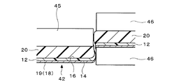
(2)この電子部品の製造方法において、
前記線は、前記貫通穴とオーバーラップする領域内で、前記補強部材の外周と交差していてもよい。
(3)この電子部品の製造方法において、
前記配線パターンは、前記補強部材とオーバーラップする領域を通る複数の配線を含み、
前記線は、前記補強部材とオーバーラップする領域内で、前記配線と交差していてもよい。
(4)この電子部品の製造方法において、
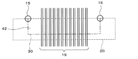
せん断加工によって、前記配線基板を、前記貫通穴と交差する前記線に沿って切ってもよい。
(5)この電子部品の製造方法において、
前記せん断加工によって、前記配線基板に、前記線に沿って延びる開口を形成してもよい。
(6)この電子部品の製造方法において、
前記せん断加工は、前記配線基板における前記開口が形成される領域を、前記第1の面側から押圧することを含んでもよい。
(7)この電子部品の製造方法において、
前記配線基板は、前記線に囲まれた第1の部分と、前記線の外側の第2の部分とを含み、
前記せん断加工によって、前記配線基板から前記第1の部分を打ち抜くことを含んでもよい。
(8)この電子部品の製造方法において、
前記せん断加工は、前記補強部材の前記貫通穴とオーバーラップする辺と前記線とによって囲まれた領域を、前記第2の面側から押圧することを含んでもよい。
(9)この電子部品の製造方法において、
刃物を利用して、前記配線基板を、前記貫通穴と交差する前記線に沿って切ってもよい。
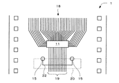
(10)本発明に係る配線基板は、ベース基板と、
前記ベース基板の第1の面に設けられた配線パターンと、
前記ベース基板の第2の面に設けられた補強部材と、
を有し、
前記ベース基板には、前記補強部材の端部と部分的にオーバーラップするように配置された貫通穴が形成されている。本発明によれば、効率よく切ることが可能な配線基板を提供することができる。
図1〜図9は、本発明を適用した第1の実施の形態に係る電子部品の製造方法について説明するための図である。
図13は、本発明を適用した第2の実施の形態に係る電子部品の製造方法について説明するための図である。
図14は、本発明を適用した第3の実施の形態に係る電子部品の製造方法について説明するための図である。
Claims (8)
- ベース基板と、前記ベース基板の第1の面に設けられた配線パターンと、前記ベース基板の第2の面に設けられた補強部材と、前記補強部材の端部と部分的にオーバーラップするように配置された、前記ベース基板を貫通する貫通穴とを有する配線基板を、前記貫通穴と交差するとともに前記補強部材の外周輪郭線の一部とオーバーラップする線に沿って切る工程を含み、
前記貫通穴は、前記線と前記補強部材の外周輪郭線との交点よりも前記配線パターンの側に位置する部分を有する電子部品の製造方法。 - 請求項1記載の電子部品の製造方法において、
前記配線パターンは、前記補強部材とオーバーラップする領域を通る配線を含み、
前記線は、前記補強部材とオーバーラップする領域内で、前記配線と交差してなる電子部品の製造方法。 - 請求項1又は請求項2のいずれかに記載の電子部品の製造方法において、
せん断加工によって、前記配線基板を、前記貫通穴と交差する前記線に沿って切る電子部品の製造方法。 - 請求項3記載の電子部品の製造方法において、
前記せん断加工によって、前記配線基板に、前記線に沿って延びる開口を形成する電子部品の製造方法。 - 請求項4記載の電子部品の製造方法において、
前記せん断加工は、前記配線基板における前記開口が形成される領域を、前記第1の面側から押圧することを含む電子部品の製造方法。 - 請求項3記載の電子部品の製造方法において、
前記配線基板は、前記線に囲まれた第1の部分と、前記線の外側の第2の部分とを含み、
前記せん断加工によって、前記配線基板から前記第1の部分を打ち抜くことを含む電子部品の製造方法。 - 請求項3から請求項6のいずれかに記載の電子部品の製造方法において、
前記せん断加工は、前記補強部材の前記貫通穴とオーバーラップする辺と前記線とによって囲まれた領域を、前記第2の面側から押圧することを含む電子部品の製造方法。 - 請求項1又は請求項2のいずれかに記載の電子部品の製造方法において、
刃物を利用して、前記配線基板を、前記貫通穴と交差する前記線に沿って切る電子部品の製造方法。
Priority Applications (3)
| Application Number | Priority Date | Filing Date | Title |
|---|---|---|---|
| JP2004334404A JP4085281B2 (ja) | 2004-11-18 | 2004-11-18 | 電子部品の製造方法 |
| US11/247,612 US7385142B2 (en) | 2004-11-18 | 2005-10-10 | Manufacturing method of electronic part and wiring substrate |
| CNB2005101201992A CN100421227C (zh) | 2004-11-18 | 2005-11-15 | 电子部件的制造方法以及布线基板 |
Applications Claiming Priority (1)
| Application Number | Priority Date | Filing Date | Title |
|---|---|---|---|
| JP2004334404A JP4085281B2 (ja) | 2004-11-18 | 2004-11-18 | 電子部品の製造方法 |
Publications (2)
| Publication Number | Publication Date |
|---|---|
| JP2006147763A JP2006147763A (ja) | 2006-06-08 |
| JP4085281B2 true JP4085281B2 (ja) | 2008-05-14 |
Family
ID=36385009
Family Applications (1)
| Application Number | Title | Priority Date | Filing Date |
|---|---|---|---|
| JP2004334404A Expired - Fee Related JP4085281B2 (ja) | 2004-11-18 | 2004-11-18 | 電子部品の製造方法 |
Country Status (3)
| Country | Link |
|---|---|
| US (1) | US7385142B2 (ja) |
| JP (1) | JP4085281B2 (ja) |
| CN (1) | CN100421227C (ja) |
Families Citing this family (6)
| Publication number | Priority date | Publication date | Assignee | Title |
|---|---|---|---|---|
| JP3915927B2 (ja) | 2004-11-18 | 2007-05-16 | セイコーエプソン株式会社 | 電子部品及びその製造方法 |
| JP3915928B2 (ja) * | 2004-11-24 | 2007-05-16 | セイコーエプソン株式会社 | 電子部品及びその製造方法 |
| JP4171926B2 (ja) | 2006-09-19 | 2008-10-29 | セイコーエプソン株式会社 | 板片付き配線基板の製造方法 |
| JP5066718B2 (ja) * | 2007-12-17 | 2012-11-07 | 住友電工プリントサーキット株式会社 | フレキシブルプリント配線板の製造方法 |
| CN103890686B (zh) * | 2011-10-25 | 2016-05-18 | 惠普发展公司,有限责任合伙企业 | 驱动器托架基板 |
| TWI745823B (zh) * | 2019-12-31 | 2021-11-11 | 頎邦科技股份有限公司 | 軟性電路板之補強結構 |
Family Cites Families (15)
| Publication number | Priority date | Publication date | Assignee | Title |
|---|---|---|---|---|
| US2361234A (en) * | 1942-03-21 | 1944-10-24 | Picard Benjamin | Engraving machine |
| JPS5648198A (en) * | 1979-09-26 | 1981-05-01 | Matsushita Electric Ind Co Ltd | Method of manufacturing flexible printed circuit board |
| US5592199A (en) * | 1993-01-27 | 1997-01-07 | Sharp Kabushiki Kaisha | Assembly structure of a flat type device including a panel having electrode terminals disposed on a peripheral portion thereof and method for assembling the same |
| JPH07321426A (ja) * | 1994-05-24 | 1995-12-08 | Casio Comput Co Ltd | フィルム配線基板およびそれを用いた電子機器 |
| JP3196195B2 (ja) * | 1996-06-12 | 2001-08-06 | 船井電機株式会社 | ケーブルホルダおよびケーブルの固定方法 |
| JPH10135581A (ja) | 1996-10-31 | 1998-05-22 | Sumitomo Electric Ind Ltd | フレキシブルプリント回路基板 |
| JP2000030784A (ja) * | 1998-05-08 | 2000-01-28 | Japan Aviation Electronics Ind Ltd | 電気コネクタ |
| JP2000124575A (ja) | 1998-08-11 | 2000-04-28 | Seiko Epson Corp | 配線基板、液晶装置及び電子機器 |
| JP3640155B2 (ja) | 1999-01-26 | 2005-04-20 | セイコーエプソン株式会社 | 可撓性配線基板、フィルムキャリア、テープ状半導体装置、半導体装置、回路基板並びに電子機器 |
| JP2001068189A (ja) * | 1999-08-27 | 2001-03-16 | Yazaki Corp | コネクタ構造 |
| JP2001148547A (ja) | 1999-11-18 | 2001-05-29 | Sanyo Electric Co Ltd | 電気装置の接続に用いるcof基板 |
| US6433414B2 (en) * | 2000-01-26 | 2002-08-13 | Casio Computer Co., Ltd. | Method of manufacturing flexible wiring board |
| US6998857B2 (en) * | 2001-09-20 | 2006-02-14 | Yamaha Corporation | Probe unit and its manufacture |
| CN1685388A (zh) * | 2002-09-25 | 2005-10-19 | 西铁城时计株式会社 | 显示设备 |
| JP2005116495A (ja) * | 2003-09-19 | 2005-04-28 | Sony Corp | フラットケーブルおよびコネクタならびに電子機器 |
-
2004
- 2004-11-18 JP JP2004334404A patent/JP4085281B2/ja not_active Expired - Fee Related
-
2005
- 2005-10-10 US US11/247,612 patent/US7385142B2/en not_active Expired - Fee Related
- 2005-11-15 CN CNB2005101201992A patent/CN100421227C/zh not_active Expired - Fee Related
Also Published As
| Publication number | Publication date |
|---|---|
| US7385142B2 (en) | 2008-06-10 |
| CN1790646A (zh) | 2006-06-21 |
| CN100421227C (zh) | 2008-09-24 |
| JP2006147763A (ja) | 2006-06-08 |
| US20060102382A1 (en) | 2006-05-18 |
Similar Documents
| Publication | Publication Date | Title |
|---|---|---|
| US20080178723A1 (en) | Semiconductor device manufacturing method and manufacturing apparatus | |
| US7535108B2 (en) | Electronic component including reinforcing member | |
| US7385142B2 (en) | Manufacturing method of electronic part and wiring substrate | |
| EP2378609A1 (en) | Film antenna and method for manufacturing the same | |
| JP3829940B2 (ja) | 半導体装置の製造方法及び製造装置 | |
| JP3915928B2 (ja) | 電子部品及びその製造方法 | |
| JP3829941B2 (ja) | 半導体装置の製造方法及び製造装置 | |
| JP2017034178A (ja) | 多層基板、部品実装基板及び部品実装基板の製造方法 | |
| JP2011009271A (ja) | プリント配線基板及びその製造方法 | |
| US7691276B2 (en) | Method for manufacturing an electrical connecting element, and a connecting element | |
| JP2007019078A (ja) | フレキシブルプリント配線板、プリント回路板、およびフレキシブルプリント配線板の製造方法 | |
| CN100499054C (zh) | 半导体装置及其制造方法 | |
| JP2007165752A (ja) | プリント配線板およびその接続構造 | |
| JP2010212320A (ja) | フレキシブルプリント配線板 | |
| JP2007273321A (ja) | 可動接点体の製造方法 | |
| JP3565142B2 (ja) | 配線基板及びその製造方法、半導体装置、回路基板並びに電子機器 | |
| JP2007249780A (ja) | コンビネーションカード及びその製造方法 | |
| JPH11126964A (ja) | 異方導電性接着剤付き可撓性回路基板および製造方法 | |
| JP4526813B2 (ja) | 接合体の製造方法 | |
| JP6089614B2 (ja) | 樹脂多層基板 | |
| JP2007142177A (ja) | 電子部品の製造方法及び配線基板 |
Legal Events
| Date | Code | Title | Description |
|---|---|---|---|
| A977 | Report on retrieval |
Free format text: JAPANESE INTERMEDIATE CODE: A971007 Effective date: 20070621 |
|
| A131 | Notification of reasons for refusal |
Free format text: JAPANESE INTERMEDIATE CODE: A131 Effective date: 20070627 |
|
| A521 | Request for written amendment filed |
Free format text: JAPANESE INTERMEDIATE CODE: A523 Effective date: 20070820 |
|
| TRDD | Decision of grant or rejection written | ||
| A01 | Written decision to grant a patent or to grant a registration (utility model) |
Free format text: JAPANESE INTERMEDIATE CODE: A01 Effective date: 20080123 |
|
| A61 | First payment of annual fees (during grant procedure) |
Free format text: JAPANESE INTERMEDIATE CODE: A61 Effective date: 20080205 |
|
| FPAY | Renewal fee payment (event date is renewal date of database) |
Free format text: PAYMENT UNTIL: 20110228 Year of fee payment: 3 |
|
| R150 | Certificate of patent or registration of utility model |
Free format text: JAPANESE INTERMEDIATE CODE: R150 |
|
| FPAY | Renewal fee payment (event date is renewal date of database) |
Free format text: PAYMENT UNTIL: 20110228 Year of fee payment: 3 |
|
| FPAY | Renewal fee payment (event date is renewal date of database) |
Free format text: PAYMENT UNTIL: 20120229 Year of fee payment: 4 |
|
| FPAY | Renewal fee payment (event date is renewal date of database) |
Free format text: PAYMENT UNTIL: 20130228 Year of fee payment: 5 |
|
| FPAY | Renewal fee payment (event date is renewal date of database) |
Free format text: PAYMENT UNTIL: 20130228 Year of fee payment: 5 |
|
| LAPS | Cancellation because of no payment of annual fees |