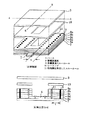
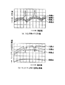
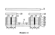
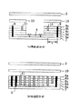
JP4013432B2 - 半導体パッケージ - Google Patents
半導体パッケージ Download PDFInfo
- Publication number
- JP4013432B2 JP4013432B2 JP2000002594A JP2000002594A JP4013432B2 JP 4013432 B2 JP4013432 B2 JP 4013432B2 JP 2000002594 A JP2000002594 A JP 2000002594A JP 2000002594 A JP2000002594 A JP 2000002594A JP 4013432 B2 JP4013432 B2 JP 4013432B2
- Authority
- JP
- Japan
- Prior art keywords
- cavity
- semiconductor package
- holes
- back conductive
- dielectric
- Prior art date
- Legal status (The legal status is an assumption and is not a legal conclusion. Google has not performed a legal analysis and makes no representation as to the accuracy of the status listed.)
- Expired - Fee Related
Links
Images


Landscapes
- Microwave Amplifiers (AREA)
Priority Applications (1)
| Application Number | Priority Date | Filing Date | Title |
|---|---|---|---|
| JP2000002594A JP4013432B2 (ja) | 2000-01-11 | 2000-01-11 | 半導体パッケージ |
Applications Claiming Priority (1)
| Application Number | Priority Date | Filing Date | Title |
|---|---|---|---|
| JP2000002594A JP4013432B2 (ja) | 2000-01-11 | 2000-01-11 | 半導体パッケージ |
Publications (3)
| Publication Number | Publication Date |
|---|---|
| JP2001196500A JP2001196500A (ja) | 2001-07-19 |
| JP2001196500A5 JP2001196500A5 (enExample) | 2006-12-21 |
| JP4013432B2 true JP4013432B2 (ja) | 2007-11-28 |
Family
ID=18531684
Family Applications (1)
| Application Number | Title | Priority Date | Filing Date |
|---|---|---|---|
| JP2000002594A Expired - Fee Related JP4013432B2 (ja) | 2000-01-11 | 2000-01-11 | 半導体パッケージ |
Country Status (1)
| Country | Link |
|---|---|
| JP (1) | JP4013432B2 (enExample) |
Families Citing this family (4)
| Publication number | Priority date | Publication date | Assignee | Title |
|---|---|---|---|---|
| WO2006001389A1 (ja) * | 2004-06-28 | 2006-01-05 | Mitsubishi Denki Kabushiki Kaisha | 多層誘電体基板および半導体パッケージ |
| KR100650732B1 (ko) | 2004-12-28 | 2006-11-27 | 주식회사 하이닉스반도체 | 스택 칩 패키지 |
| CN101971327B (zh) * | 2008-03-17 | 2012-07-18 | 三菱电机株式会社 | 多层介质基板及半导体封装 |
| JP5377096B2 (ja) | 2008-09-08 | 2013-12-25 | 株式会社東芝 | 高周波パッケージ装置およびその製造方法 |
-
2000
- 2000-01-11 JP JP2000002594A patent/JP4013432B2/ja not_active Expired - Fee Related
Also Published As
| Publication number | Publication date |
|---|---|
| JP2001196500A (ja) | 2001-07-19 |
Similar Documents
| Publication | Publication Date | Title |
|---|---|---|
| KR100361432B1 (ko) | 비가역회로장치 | |
| US10622693B2 (en) | Filter unit and filter | |
| CN111010116B (zh) | 带有高度渐变的凸起结构的体声波谐振器、滤波器和电子设备 | |
| JP2019057852A (ja) | 複合電子部品 | |
| JP5616927B2 (ja) | ホーンアンテナ一体型mmicパッケージ及びアレーアンテナ | |
| JPH1093308A (ja) | 非可逆回路素子 | |
| TW418552B (en) | Dielectric filter, transmitting/receiving device and communication device | |
| JP2002353708A (ja) | 伝送線路、集積回路および送受信装置 | |
| JPH09252206A (ja) | 誘電体フィルタ | |
| JP4013432B2 (ja) | 半導体パッケージ | |
| JP2011139244A (ja) | 高周波モジュール | |
| JPH09321501A (ja) | 多層高周波回路基板 | |
| JP2571029B2 (ja) | マイクロ波集積回路 | |
| JP2010272585A (ja) | フリップチップ実装構造 | |
| JP3307293B2 (ja) | 非可逆回路素子 | |
| WO2014087792A1 (ja) | 高周波モジュール | |
| JP2001196502A (ja) | 半導体パッケージ | |
| JP2001358501A (ja) | ストリップ線路フィルタ | |
| JP2008277336A (ja) | 半導体パッケージ | |
| KR102336512B1 (ko) | 내부 정합형 반도체 패키지 | |
| JP2001053508A (ja) | 高周波回路部品の実装構造 | |
| JP3932920B2 (ja) | アンテナ一体型高周波回路モジュール | |
| JP3438726B2 (ja) | パッケージ | |
| JP6601129B2 (ja) | 誘電体共振装置及びそれを用いた実装構造体 | |
| JP4401886B2 (ja) | 高周波用パッケージ |
Legal Events
| Date | Code | Title | Description |
|---|---|---|---|
| A521 | Written amendment |
Free format text: JAPANESE INTERMEDIATE CODE: A523 Effective date: 20060830 |
|
| A621 | Written request for application examination |
Free format text: JAPANESE INTERMEDIATE CODE: A621 Effective date: 20060830 |
|
| RD01 | Notification of change of attorney |
Free format text: JAPANESE INTERMEDIATE CODE: A7421 Effective date: 20060906 |
|
| A521 | Written amendment |
Free format text: JAPANESE INTERMEDIATE CODE: A523 Effective date: 20061101 |
|
| A977 | Report on retrieval |
Free format text: JAPANESE INTERMEDIATE CODE: A971007 Effective date: 20070307 |
|
| A131 | Notification of reasons for refusal |
Free format text: JAPANESE INTERMEDIATE CODE: A131 Effective date: 20070522 |
|
| A521 | Written amendment |
Free format text: JAPANESE INTERMEDIATE CODE: A523 Effective date: 20070719 |
|
| TRDD | Decision of grant or rejection written | ||
| A01 | Written decision to grant a patent or to grant a registration (utility model) |
Free format text: JAPANESE INTERMEDIATE CODE: A01 Effective date: 20070821 |
|
| A61 | First payment of annual fees (during grant procedure) |
Free format text: JAPANESE INTERMEDIATE CODE: A61 Effective date: 20070903 |
|
| FPAY | Renewal fee payment (event date is renewal date of database) |
Free format text: PAYMENT UNTIL: 20100921 Year of fee payment: 3 |
|
| FPAY | Renewal fee payment (event date is renewal date of database) |
Free format text: PAYMENT UNTIL: 20100921 Year of fee payment: 3 |
|
| FPAY | Renewal fee payment (event date is renewal date of database) |
Free format text: PAYMENT UNTIL: 20110921 Year of fee payment: 4 |
|
| FPAY | Renewal fee payment (event date is renewal date of database) |
Free format text: PAYMENT UNTIL: 20110921 Year of fee payment: 4 |
|
| FPAY | Renewal fee payment (event date is renewal date of database) |
Free format text: PAYMENT UNTIL: 20120921 Year of fee payment: 5 |
|
| FPAY | Renewal fee payment (event date is renewal date of database) |
Free format text: PAYMENT UNTIL: 20130921 Year of fee payment: 6 |
|
| LAPS | Cancellation because of no payment of annual fees |