JP4013432B2 - Semiconductor package - Google Patents
Semiconductor package Download PDFInfo
- Publication number
- JP4013432B2 JP4013432B2 JP2000002594A JP2000002594A JP4013432B2 JP 4013432 B2 JP4013432 B2 JP 4013432B2 JP 2000002594 A JP2000002594 A JP 2000002594A JP 2000002594 A JP2000002594 A JP 2000002594A JP 4013432 B2 JP4013432 B2 JP 4013432B2
- Authority
- JP
- Japan
- Prior art keywords
- cavity
- semiconductor package
- holes
- back conductive
- dielectric
- Prior art date
- Legal status (The legal status is an assumption and is not a legal conclusion. Google has not performed a legal analysis and makes no representation as to the accuracy of the status listed.)
- Expired - Fee Related
Links
Images


Description
【0001】
【発明の属する技術分野】
この発明は、高周波数帯で動作するマイクロ波、ミリ波集積回路を封止するパッケージに関するものである。
【0002】
【従来の技術】
図6、図7、図8は従来の半導体パッケージを示す図である。図において、1は金属製の箱体、2は入出力端子、3はキャップ、4は半導体素子及び誘電体回路基板、5は抵抗体である。
【0003】
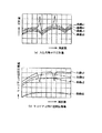
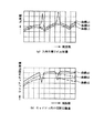
また、図9は従来の半導体パッケージの特性を示す図である。図において、曲線a1,a2は図6のようにキャビティ内に抵抗体5を設けない場合、曲線b1,b2は図7のようにキャビティ側壁に抵抗体5を設けた場合、曲線c1,c2は図8のようにキャップ3の裏面に抵抗体5を設けた場合、の入出力端子2における反射特性及びキャビティ内空間伝播特性である。
【0004】
次に、従来の半導体パッケージの動作及び特性について説明する。従来の半導体パッケージは、図6、図7、図8のように箱体1に形成したキャビティに半導体素子及び誘電体回路基板4を配置し、出力端子2を設けて、パッケージ内部に配置した半導体素子及び誘電体回路基板4と外部とを電気的に接続する。さらにキャップ3で封止することにより気密構造とする。このような半導体パッケージでは、キャビティ内寸法により、遮断周波数の決まる導波管伝送モード及び共振周波数の決まる導波管共振モードが存在し、この共振周波数を有する信号がこのキャビティに蓄えられる。この信号が、半導体素子及び誘電体回路基板4に結合した場合、異常発振や破壊を招き、外部の回路等にも悪影響を与える。したがって、従来のパッケージでは、図7及び図8のように、キャビティ内に抵抗体5を設けることにより、共振を抑圧していた。
【0005】
次に、従来の半導体パッケージの特性について補足する。従来の各半導体パッケージの入出力端子2における反射特性は、図9の曲線a1、曲線b1及び曲線c1のようになり、キャビティに抵抗体5がない場合(図6の場合、曲線a1)は共振周波数を有し、キャビティ抵抗体5がある場合(図7及び図8の場合、曲線b1及びc1)は共振を抑えることが可能になる。また、従来の各半導体パッケージの空間伝播特性は図9の曲線a2、曲線b2及び曲線c2のようになり、キャビティに抵抗体5がない場合(図6の場合、曲線a2)は異常発振が起こり、キャビティに抵抗体5がある場合(図7及び図8の場合、曲線b2及びc2)でも高い空間アイソレーションが確保できない(伝播特性の損失を大きくできない)ため、半導体素子及び誘電体回路基板4の利得が高い場合、または安定性が低い場合、空間アイソレーションの低い周波数帯と結合すると異常発振、破壊等が起こる可能性がある。このように、従来の半導体パッケージでは、キャビティ内に抵抗体5を設けることで共振を抑圧していたが、高い空間アイソレーションを確保できないため、高利得の半導体回路等を実装した場合、異常発振、破壊等が起こる可能性があり、問題となっていた。
【0006】
【発明が解決しようとする課題】
上記のように、従来の半導体パッケージでは、キャビティ内に抵抗体を設けることで共振を抑圧していたが、高い空間アイソレーションを確保できないため、高利得の半導体回路等を実装した場合、異常発振、破壊等が起こる可能性があり、課題となっていた。
【0007】
この発明はかかる課題を解決するためになされたものであり、高利得の半導体回路等を実装した場合でも、異常発振、破壊等を抑圧することが可能な半導体パッケージを提供するものである。
【0008】
【課題を解決するための手段】
第1の発明による半導体パッケージは、積層した誘電体基板内にキャビティを形成する際に設ける複数の表裏導通スルーホールから、キャビティ方向に信号周波数の概略1/4伝送波長の間隔をもって、抵抗膜を形成した複数のスルーホールを配置したものである。
【0009】
また、第2の発明による半導体パッケージは、積層した誘電体基板内にキャビティを形成する際に設ける複数の表裏導通スルーホールから、キャビティの周囲方向に信号周波数の概略1/4伝送波長の間隔をもって、抵抗膜を形成した複数のスルーホールを配置したものである。
【0010】
第3の発明による半導体パッケージは、積層した誘電体基板内にキャビティを形成する際に設ける複数の表裏導通スルーホールから、キャビティ方向及びキャビティの周囲方向の2方向に信号周波数の概略1/4伝送波長の間隔をもって、抵抗膜を形成した複数のスルーホールを配置したものである。
【0011】
また、第4の発明による半導体パッケージは、積層した誘電体基板内にキャビティを形成する際に設ける複数の表裏導通スルーホールから、キャビティ方向に信号周波数の概略1/4伝送波長の間隔をもって、抵抗膜を形成した長さの異なる複数のスルーホールを配置したものである。
【0012】
【発明の実施の形態】
実施の形態1.
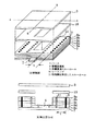
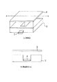
図1は、この発明の実施の形態1を示す半導体パッケージの構成図であり、図において、2は入出力端子、3はキャップ、4は半導体素子及び誘電体回路基板、7はベース、8a〜8eは積層してキャビティを構成する誘電体基板、9は表裏導通スルーホール、10はシールリング、11は抵抗膜を形成したスルーホールである。
【0013】
また、図2はこの発明の半導体パッケージの特性を示す図である。図において、曲線a1,a2,b1,b2,c1,c2は図9と同様であり、曲線d1,d2はこの発明の半導体パッケージの入出力端子2における反射特性及びキャビティ内空間伝播特性である。
【0014】
次に、動作及び特性について説明する。図1のようにベース7の上に誘電体基板8a〜8eを積層し表裏導通スルーホール9によってキャビティを形成する。また、出力端子2を設けてパッケージ内部に配置した半導体素子及び誘電体回路基板4と外部とを電気的に接続する。さらにシールリング10とキャップ3とで封止することにより気密構造とする。抵抗膜を形成したスルーホール11は、表裏導通スルーホール9からキャビティ方向に、信号周波数F0の概略1/4伝送波長の間隔tをもって配置され、このキャビティにおける共振を抑圧する。
【0015】
次に、この発明の半導体パッケージの特性について補足する。図2において、曲線a1,a2,b1,b2,c1,c2は、従来の技術(図9)にて説明したとおりである。曲線d1は、この発明の半導体パッケージの入出力端子2における反射特性であり、曲線d2はキャビティ内の空間伝播特性である。図のように、この半導体パッケージによると、キャビティ内寸法による共振を抑えることができ、空間伝播特性についても、高い空間アイソレーションを確保することができるため、高利得の半導体回路等を実装した場合でも、異常発振、破壊等を抑圧することが可能になる。
【0016】
また、抵抗膜を形成した複数のスルーホール11の配置間隔により、空間伝播特性の調整が可能である。
【0017】
なお、ベース7及びシールリング10のない半導体パッケージにおいても、上記と同等の効果が得られる。
【0018】
実施の形態2.
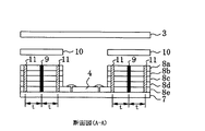
図3は、この発明の実施の形態2を示す半導体パッケージの構成図であり、図において、3はキャップ、4は半導体素子及び誘電体回路基板、7はベース、8a〜8eは積層してキャビティを構成する誘電体基板、9は表裏導通スルーホール、10はシールリング、11は抵抗膜を形成したスルーホールである。
【0019】
次に、動作及び特性について説明する。図3のようにベース7の上に誘電体基板8a〜8eを積層し表裏導通スルーホール9によってキャビティを形成する。また、出力端子(図中では省略)を設けてパッケージ内部に配置した半導体素子及び誘電体回路基板4と外部とを電気的に接続する。さらにシールリング10とキャップ3とで封止することにより気密構造とする。抵抗膜を形成したスルーホール11は、表裏導通スルーホール9からキャビティの周囲方向に、信号周波数F0の概略1/4伝送波長の間隔tをもって配置され、図2の曲線d1および曲線d2のように、このキャビティにおける共振を抑圧し、また空間伝播特性についても、高い空間アイソレーションを確保することができる。したがって、この半導体パッケージによると、キャビティ内部に高利得の半導体回路等を実装した場合でも、異常発振、破壊等を抑圧することが可能になる。
【0020】
実施の形態3.
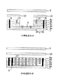
図4は、この発明の実施の形態3を示す半導体パッケージの構成図であり、図において、3はキャップ、4は半導体素子及び誘電体回路基板、7はベース、8a〜8eは積層してキャビティを構成する誘電体基板、9は表裏導通スルーホール、10はシールリング、11は抵抗膜を形成したスルーホールである。
【0021】
次に、動作及び特性について説明する。図4のようにベース7の上に誘電体基板8a〜8eを積層し表裏導通スルーホール9によってキャビティを形成する。また、出力端子(図中では省略)を設けてパッケージ内部に配置した半導体素子及び誘電体回路基板4と外部とを電気的に接続する。さらにシールリング10とキャップ3とで封止することにより気密構造とする。抵抗膜を形成したスルーホール11は、表裏導通スルーホール9からキャビティ方向及びキャビティの周囲方向の2方向に、信号周波数F0の概略1/4伝送波長の間隔tをもって配置され、図2の曲線d1および曲線d2のように、このキャビティにおける共振を抑圧し、また空間伝播特性についても、高い空間アイソレーションを確保することができる。したがって、この半導体パッケージによると、キャビティ内部に高利得の半導体回路等を実装した場合でも、異常発振、破壊等を抑圧することが可能になる。また、複数のキャビティが隣接した場合でも、キャビティの周囲方向に設けた、抵抗膜を形成したスルーホール11によって、隣接したキャビティへの信号の漏れ出しを抑圧することができる。
【0022】
実施の形態4.
図5は、この発明の実施の形態4を示す半導体パッケージの構成図であり、3はキャップ、4は半導体素子及び誘電体回路基板、7はベース、8a〜8eは積層してキャビティを構成する誘電体基板、9は表裏導通スルーホール、10はシールリング、11は抵抗膜を形成したスルーホールである。
【0023】
次に、動作及び特性について説明する。図5のようにベース7の上に誘電体基板8a〜8eを積層し表裏導通スルーホール9によってキャビティを形成する。また、出力端子(図中では省略)を設けてパッケージ内部に配置した半導体素子及び誘電体回路基板4と外部とを電気的に接続する。さらにシールリング10とキャップ3とで封止することにより気密構造とする。
抵抗膜を形成したスルーホール11は、表裏導通スルーホール9からキャビティ方向に、信号周波数F0の概略1/4伝送波長の間隔tをもって配置され、図2の曲線d1および曲線d2のように、このキャビティにおける共振を抑圧し、また空間伝播特性についても、高い空間アイソレーションを確保することができる。したがって、この半導体パッケージによると、キャビティ内部に高利得の半導体回路等を実装した場合でも、異常発振、破壊等を抑圧することが可能になる。
【0024】
また、実施の形態1〜3では、抵抗膜を形成した複数のスルーホール11によって囲まれる誘電体を含む空間の寸法により、新たに導波管伝送モード及び導波管共振モードが発生するため、共振を発生する可能性がある。しかし、本実施の形態4の半導体パッケージによると、抵抗膜を形成した複数のスルーホール11の長さが異なるため、この抵抗膜を形成した複数のスルーホール11によって囲まれる空間を形成せず、新たに導波管伝送モード及び導波管共振モードが発生しない。したがって、この半導体パッケージによると、キャビティにおける共振の抑圧、高い空間アイソレーションの確保が、より効果的に達成できる。
【0025】
【発明の効果】
第1の発明によれば、積層した誘電体基板内にキャビティを形成するために設ける複数の表裏導通スルーホールから、キャビティ方向に信号周波数の概略1/4伝送波長の間隔をもって、抵抗膜を形成した複数のスルーホールを配置したことにより、キャビティ内寸法による共振を抑えることができ、空間伝播特性についても、高い空間アイソレーションを確保することができるため、高利得の半導体回路等を実装した場合でも、異常発振、破壊等を抑圧することが可能になる。
【0026】
また、第2の発明によれば、積層した誘電体基板内にキャビティを形成するために設ける複数の表裏導通スルーホールから、キャビティの周囲方向に信号周波数の概略1/4伝送波長の間隔をもって、抵抗膜を形成した複数のスルーホールを配置したことにより、キャビティ内寸法による共振を抑えることができ、空間伝播特性についても、高い空間アイソレーションを確保することができるため、高利得の半導体回路等を実装した場合でも、異常発振、破壊等を抑圧することが可能になる。
【0027】
第3の発明によれば、積層した誘電体基板内にキャビティを形成するために設ける複数の表裏導通スルーホールから、キャビティ方向及びキャビティの周囲方向の2方向に信号周波数の概略1/4伝送波長の間隔をもって、抵抗膜を形成した複数のスルーホールを配置したことにより、キャビティ内寸法による共振を抑えることができ、空間伝播特性についても、高い空間アイソレーションを確保することができるため、高利得の半導体回路等を実装した場合でも、異常発振、破壊等を抑圧することが可能になる。また、複数のキャビティが隣接した場合でも、隣接したキャビティへの信号の漏れ出しを抑圧することができる。
【0028】
また、第4の発明によれば、積層した誘電体基板内にキャビティを形成するために設ける複数の表裏導通スルーホールから、キャビティ方向に信号周波数の概略1/4伝送波長の間隔をもって、抵抗膜を形成した長さの異なる複数のスルーホールを配置したことにより、第1〜第3の発明よりも、効果的にキャビティ内寸法による共振を抑えることができ、空間伝播特性についても、高い空間アイソレーションを確保することができるため、高利得の半導体回路等を実装した場合でも、異常発振、破壊等を抑圧することが可能になる。
【図面の簡単な説明】
【図1】 この発明による半導体パッケージの実施の形態1を示す図である。
【図2】 この発明による半導体パッケージの特性を示す図である。
【図3】 この発明による半導体パッケージの実施の形態2を示す図である。
【図4】 この発明による半導体パッケージの実施の形態3を示す図である。
【図5】 この発明による半導体パッケージの実施の形態4を示す図である。
【図6】 従来の半導体パッケージの一例を示す図である。
【図7】 従来の半導体パッケージの一例を示す図である。
【図8】 従来の半導体パッケージの一例を示す図である。
【図9】 従来の半導体パッケージの特性を示す図である。
【符号の説明】
7 ベース、8a 誘電体基板、8b 誘電体基板、8c 誘電体基板、8d誘電体基板、8e 誘電体基板、9 表裏導通スルーホール、10 シールリング、11 抵抗膜を形成したスルーホール。[0001]
BACKGROUND OF THE INVENTION
The present invention relates to a package for sealing a microwave or millimeter wave integrated circuit operating in a high frequency band.
[0002]
[Prior art]
6, 7 and 8 are views showing a conventional semiconductor package. In the figure, 1 is a metal box, 2 is an input / output terminal, 3 is a cap, 4 is a semiconductor element and a dielectric circuit board, and 5 is a resistor.
[0003]
FIG. 9 is a diagram showing characteristics of a conventional semiconductor package. In the figure, the curves a1 and a2 are when the
[0004]
Next, the operation and characteristics of a conventional semiconductor package will be described. A conventional semiconductor package is a semiconductor in which a semiconductor element and a dielectric circuit board 4 are arranged in a cavity formed in a
[0005]
Next, the characteristics of the conventional semiconductor package will be supplemented. The reflection characteristics at the input /
[0006]
[Problems to be solved by the invention]
As described above, in the conventional semiconductor package, the resonance was suppressed by providing a resistor in the cavity. However, because high spatial isolation cannot be secured, abnormal oscillation occurs when a high gain semiconductor circuit is mounted. There is a possibility that destruction, etc. may occur, which has been a problem.
[0007]
The present invention has been made to solve such a problem, and provides a semiconductor package capable of suppressing abnormal oscillation, destruction, and the like even when a high-gain semiconductor circuit or the like is mounted.
[0008]
[Means for Solving the Problems]
According to a first aspect of the present invention, there is provided a semiconductor package having a resistive film with a spacing of approximately 1/4 transmission wavelength of a signal frequency in a cavity direction from a plurality of front and back conductive through holes provided when a cavity is formed in a laminated dielectric substrate. A plurality of formed through holes are arranged.
[0009]
The semiconductor package according to the second invention has an interval of approximately 1/4 transmission wavelength of the signal frequency in the circumferential direction of the cavity from a plurality of front and back conductive through holes provided when the cavity is formed in the laminated dielectric substrate. A plurality of through holes in which a resistance film is formed are arranged.
[0010]
According to a third aspect of the present invention, there is provided a semiconductor package in which approximately 1/4 transmission of a signal frequency is performed in two directions, a cavity direction and a cavity peripheral direction, from a plurality of front and back conductive through holes provided when a cavity is formed in a laminated dielectric substrate. A plurality of through-holes in which a resistance film is formed are arranged with wavelength intervals.
[0011]
According to a fourth aspect of the present invention, there is provided a semiconductor package having a resistance of approximately 1/4 transmission wavelength of a signal frequency in a cavity direction from a plurality of front and back conductive through holes provided when a cavity is formed in a laminated dielectric substrate. A plurality of through holes having different lengths in which a film is formed are arranged.
[0012]
DETAILED DESCRIPTION OF THE INVENTION
FIG. 1 is a configuration diagram of a semiconductor
[0013]
FIG. 2 is a diagram showing the characteristics of the semiconductor package of the present invention. In the figure, curves a1, a2, b1, b2, c1, and c2 are the same as those in FIG. 9, and curves d1 and d2 are reflection characteristics and intra-cavity space propagation characteristics at the input /
[0014]
Next, the operation and characteristics will be described. As shown in FIG. 1,
[0015]
Next, the characteristics of the semiconductor package of the present invention will be supplemented. In FIG. 2, curves a1, a2, b1, b2, c1, and c2 are as described in the prior art (FIG. 9). A curve d1 is a reflection characteristic at the input /
[0016]
Further, the spatial propagation characteristics can be adjusted by the arrangement interval of the plurality of through
[0017]
Even in a semiconductor package without the
[0018]
FIG. 3 is a configuration diagram of a semiconductor
[0019]
Next, the operation and characteristics will be described. As shown in FIG. 3,
[0020]
FIG. 4 is a configuration diagram of a semiconductor
[0021]
Next, the operation and characteristics will be described. As shown in FIG. 4,
[0022]
Embodiment 4 FIG.
FIG. 5 is a configuration diagram of a semiconductor package showing Embodiment 4 of the present invention. 3 is a cap, 4 is a semiconductor element and a dielectric circuit board, 7 is a base, and 8a to 8e are stacked to form a cavity. A dielectric substrate, 9 is a through hole on the front and back sides, 10 is a seal ring, and 11 is a through hole in which a resistance film is formed.
[0023]
Next, the operation and characteristics will be described. As shown in FIG. 5,
The through
[0024]
In the first to third embodiments, a waveguide transmission mode and a waveguide resonance mode are newly generated due to the size of the space including the dielectric surrounded by the plurality of through
[0025]
【The invention's effect】
According to the first aspect of the present invention, the resistive film is formed at intervals of approximately 1/4 transmission wavelength of the signal frequency in the cavity direction from the plurality of front and back conductive through holes provided to form the cavity in the laminated dielectric substrate. By arranging multiple through-holes, resonance due to the dimensions in the cavity can be suppressed and high spatial isolation can be secured for spatial propagation characteristics. However, it is possible to suppress abnormal oscillation, destruction, and the like.
[0026]
Further, according to the second invention, from a plurality of front and back conductive through holes provided to form a cavity in the laminated dielectric substrate, with an interval of approximately 1/4 transmission wavelength of the signal frequency in the circumferential direction of the cavity, By arranging a plurality of through-holes with a resistive film, resonance due to the dimensions in the cavity can be suppressed, and high spatial isolation can be ensured for spatial propagation characteristics. Even when is mounted, abnormal oscillation, destruction, etc. can be suppressed.
[0027]
According to the third aspect of the invention, from a plurality of front and back conductive through holes provided for forming a cavity in the laminated dielectric substrate, approximately 1/4 transmission wavelength of the signal frequency in the cavity direction and the circumferential direction of the cavity. By arranging a plurality of through-holes with a resistive film at an interval of, it is possible to suppress resonance due to the dimensions in the cavity and to ensure high spatial isolation in terms of spatial propagation characteristics. Even when the semiconductor circuit is mounted, it is possible to suppress abnormal oscillation, destruction, and the like. Further, even when a plurality of cavities are adjacent to each other, signal leakage to the adjacent cavities can be suppressed.
[0028]
According to the fourth aspect of the present invention, the resistive film has an interval of approximately 1/4 transmission wavelength of the signal frequency in the cavity direction from the plurality of front and back conductive through holes provided for forming the cavity in the laminated dielectric substrate. By arranging a plurality of through-holes having different lengths, it is possible to more effectively suppress resonance due to the dimensions in the cavity than in the first to third inventions, and also to achieve high spatial isotropy in terms of spatial propagation characteristics. Therefore, even when a high gain semiconductor circuit or the like is mounted, it is possible to suppress abnormal oscillation, destruction, and the like.
[Brief description of the drawings]
FIG. 1 is a diagram showing a first embodiment of a semiconductor package according to the present invention.
FIG. 2 is a diagram showing characteristics of a semiconductor package according to the present invention.
FIG. 3 is a diagram showing a second embodiment of a semiconductor package according to the present invention.
FIG. 4 is a diagram showing a third embodiment of a semiconductor package according to the present invention.
FIG. 5 is a diagram showing a semiconductor package according to a fourth embodiment of the present invention.
FIG. 6 is a diagram showing an example of a conventional semiconductor package.
FIG. 7 is a diagram showing an example of a conventional semiconductor package.
FIG. 8 is a diagram showing an example of a conventional semiconductor package.
FIG. 9 is a diagram showing characteristics of a conventional semiconductor package.
[Explanation of symbols]
7 Base, 8a Dielectric substrate, 8b Dielectric substrate, 8c Dielectric substrate, 8d Dielectric substrate, 8e Dielectric substrate, 9 Front and back conductive through hole, 10 Seal ring, 11 Through hole in which a resistance film is formed.
Claims (4)
Priority Applications (1)
| Application Number | Priority Date | Filing Date | Title |
|---|---|---|---|
| JP2000002594A JP4013432B2 (en) | 2000-01-11 | 2000-01-11 | Semiconductor package |
Applications Claiming Priority (1)
| Application Number | Priority Date | Filing Date | Title |
|---|---|---|---|
| JP2000002594A JP4013432B2 (en) | 2000-01-11 | 2000-01-11 | Semiconductor package |
Publications (3)
| Publication Number | Publication Date |
|---|---|
| JP2001196500A JP2001196500A (en) | 2001-07-19 |
| JP2001196500A5 JP2001196500A5 (en) | 2006-12-21 |
| JP4013432B2 true JP4013432B2 (en) | 2007-11-28 |
Family
ID=18531684
Family Applications (1)
| Application Number | Title | Priority Date | Filing Date |
|---|---|---|---|
| JP2000002594A Expired - Fee Related JP4013432B2 (en) | 2000-01-11 | 2000-01-11 | Semiconductor package |
Country Status (1)
| Country | Link |
|---|---|
| JP (1) | JP4013432B2 (en) |
Families Citing this family (4)
| Publication number | Priority date | Publication date | Assignee | Title |
|---|---|---|---|---|
| WO2006001389A1 (en) * | 2004-06-28 | 2006-01-05 | Mitsubishi Denki Kabushiki Kaisha | Multilayer dielectric substrate and semiconductor package |
| KR100650732B1 (en) | 2004-12-28 | 2006-11-27 | 주식회사 하이닉스반도체 | stacked chip package |
| WO2009116403A1 (en) * | 2008-03-17 | 2009-09-24 | 三菱電機株式会社 | Multilayer dielectric substrate, and semiconductor package |
| JP5377096B2 (en) | 2008-09-08 | 2013-12-25 | 株式会社東芝 | High frequency package device and manufacturing method thereof |
-
2000
- 2000-01-11 JP JP2000002594A patent/JP4013432B2/en not_active Expired - Fee Related
Also Published As
| Publication number | Publication date |
|---|---|
| JP2001196500A (en) | 2001-07-19 |
Similar Documents
| Publication | Publication Date | Title |
|---|---|---|
| US10622693B2 (en) | Filter unit and filter | |
| JP2000323601A (en) | Electronic part and package therefor | |
| TW418552B (en) | Dielectric filter, transmitting/receiving device and communication device | |
| JP2019057852A (en) | Composite electronic component | |
| JP2002353708A (en) | Transmission line, integrated circuit and transmitter- receiver | |
| JP4013432B2 (en) | Semiconductor package | |
| JP5342995B2 (en) | High frequency module | |
| JPH09252206A (en) | Dielectric filter | |
| JPH09321501A (en) | Multilayer high frequency circuit board | |
| WO2014087792A1 (en) | High-frequency module | |
| JPH06236935A (en) | Package for microwave circuit | |
| JP2001196502A (en) | Semiconductor package | |
| JP2010272585A (en) | Flip-chip mounting structure | |
| JP3916988B2 (en) | High frequency module | |
| KR102336512B1 (en) | Internally matched semiconductor package | |
| JP2001358501A (en) | Stripline filter | |
| JP2009212309A (en) | Semiconductor package | |
| JP2001053508A (en) | Mounting structure for high-frequency circuit component | |
| JP6601129B2 (en) | Dielectric resonator and mounting structure using the same | |
| JP3932920B2 (en) | Antenna integrated high-frequency circuit module | |
| JP3438726B2 (en) | package | |
| JP4401886B2 (en) | High frequency package | |
| JP2008277336A (en) | Semiconductor package | |
| JPH05110310A (en) | Microwave circuit | |
| JP2004297764A (en) | Bandpass filter |
Legal Events
| Date | Code | Title | Description |
|---|---|---|---|
| A521 | Written amendment |
Free format text: JAPANESE INTERMEDIATE CODE: A523 Effective date: 20060830 |
|
| A621 | Written request for application examination |
Free format text: JAPANESE INTERMEDIATE CODE: A621 Effective date: 20060830 |
|
| RD01 | Notification of change of attorney |
Free format text: JAPANESE INTERMEDIATE CODE: A7421 Effective date: 20060906 |
|
| A521 | Written amendment |
Free format text: JAPANESE INTERMEDIATE CODE: A523 Effective date: 20061101 |
|
| A977 | Report on retrieval |
Free format text: JAPANESE INTERMEDIATE CODE: A971007 Effective date: 20070307 |
|
| A131 | Notification of reasons for refusal |
Free format text: JAPANESE INTERMEDIATE CODE: A131 Effective date: 20070522 |
|
| A521 | Written amendment |
Free format text: JAPANESE INTERMEDIATE CODE: A523 Effective date: 20070719 |
|
| TRDD | Decision of grant or rejection written | ||
| A01 | Written decision to grant a patent or to grant a registration (utility model) |
Free format text: JAPANESE INTERMEDIATE CODE: A01 Effective date: 20070821 |
|
| A61 | First payment of annual fees (during grant procedure) |
Free format text: JAPANESE INTERMEDIATE CODE: A61 Effective date: 20070903 |
|
| FPAY | Renewal fee payment (event date is renewal date of database) |
Free format text: PAYMENT UNTIL: 20100921 Year of fee payment: 3 |
|
| FPAY | Renewal fee payment (event date is renewal date of database) |
Free format text: PAYMENT UNTIL: 20100921 Year of fee payment: 3 |
|
| FPAY | Renewal fee payment (event date is renewal date of database) |
Free format text: PAYMENT UNTIL: 20110921 Year of fee payment: 4 |
|
| FPAY | Renewal fee payment (event date is renewal date of database) |
Free format text: PAYMENT UNTIL: 20110921 Year of fee payment: 4 |
|
| FPAY | Renewal fee payment (event date is renewal date of database) |
Free format text: PAYMENT UNTIL: 20120921 Year of fee payment: 5 |
|
| FPAY | Renewal fee payment (event date is renewal date of database) |
Free format text: PAYMENT UNTIL: 20130921 Year of fee payment: 6 |
|
| LAPS | Cancellation because of no payment of annual fees |