JP3953776B2 - Material discharging apparatus and method, color filter manufacturing apparatus and manufacturing method, liquid crystal device manufacturing apparatus and manufacturing method, EL apparatus manufacturing apparatus and manufacturing method - Google Patents
Material discharging apparatus and method, color filter manufacturing apparatus and manufacturing method, liquid crystal device manufacturing apparatus and manufacturing method, EL apparatus manufacturing apparatus and manufacturing method Download PDFInfo
- Publication number
- JP3953776B2 JP3953776B2 JP2001329824A JP2001329824A JP3953776B2 JP 3953776 B2 JP3953776 B2 JP 3953776B2 JP 2001329824 A JP2001329824 A JP 2001329824A JP 2001329824 A JP2001329824 A JP 2001329824A JP 3953776 B2 JP3953776 B2 JP 3953776B2
- Authority
- JP
- Japan
- Prior art keywords
- manufacturing
- heads
- head
- scanning direction
- color filter
- Prior art date
- Legal status (The legal status is an assumption and is not a legal conclusion. Google has not performed a legal analysis and makes no representation as to the accuracy of the status listed.)
- Expired - Lifetime
Links
- 239000000463 material Substances 0.000 title claims description 159
- 238000004519 manufacturing process Methods 0.000 title claims description 148
- 238000000034 method Methods 0.000 title claims description 105
- 239000004973 liquid crystal related substance Substances 0.000 title claims description 99
- 238000007599 discharging Methods 0.000 title claims description 18
- 239000000758 substrate Substances 0.000 claims description 206
- 230000007246 mechanism Effects 0.000 claims description 98
- 239000011295 pitch Substances 0.000 claims description 66
- 239000010408 film Substances 0.000 description 36
- 230000008569 process Effects 0.000 description 36
- 230000015572 biosynthetic process Effects 0.000 description 17
- 238000002347 injection Methods 0.000 description 17
- 239000007924 injection Substances 0.000 description 17
- 238000005192 partition Methods 0.000 description 15
- 238000004140 cleaning Methods 0.000 description 12
- 239000003086 colorant Substances 0.000 description 12
- 229910052751 metal Inorganic materials 0.000 description 12
- 239000002184 metal Substances 0.000 description 12
- 238000000059 patterning Methods 0.000 description 12
- 238000000206 photolithography Methods 0.000 description 12
- 230000006870 function Effects 0.000 description 10
- 239000011347 resin Substances 0.000 description 10
- 229920005989 resin Polymers 0.000 description 10
- 238000003860 storage Methods 0.000 description 10
- 239000011521 glass Substances 0.000 description 9
- 239000011159 matrix material Substances 0.000 description 9
- 239000004020 conductor Substances 0.000 description 8
- 229920003023 plastic Polymers 0.000 description 8
- 239000004065 semiconductor Substances 0.000 description 7
- 239000000956 alloy Substances 0.000 description 6
- 229910045601 alloy Inorganic materials 0.000 description 6
- 238000010586 diagram Methods 0.000 description 6
- 239000004033 plastic Substances 0.000 description 6
- 238000012545 processing Methods 0.000 description 6
- 239000003566 sealing material Substances 0.000 description 6
- 230000009471 action Effects 0.000 description 5
- 238000010438 heat treatment Methods 0.000 description 5
- 230000001681 protective effect Effects 0.000 description 5
- 239000002904 solvent Substances 0.000 description 5
- 238000000576 coating method Methods 0.000 description 4
- 238000005520 cutting process Methods 0.000 description 4
- 239000007788 liquid Substances 0.000 description 4
- 239000010409 thin film Substances 0.000 description 4
- VYPSYNLAJGMNEJ-UHFFFAOYSA-N Silicium dioxide Chemical compound O=[Si]=O VYPSYNLAJGMNEJ-UHFFFAOYSA-N 0.000 description 3
- 239000011248 coating agent Substances 0.000 description 3
- 229910052802 copper Inorganic materials 0.000 description 3
- 239000003989 dielectric material Substances 0.000 description 3
- 238000006073 displacement reaction Methods 0.000 description 3
- 230000000694 effects Effects 0.000 description 3
- NBVXSUQYWXRMNV-UHFFFAOYSA-N fluoromethane Chemical compound FC NBVXSUQYWXRMNV-UHFFFAOYSA-N 0.000 description 3
- 239000007789 gas Substances 0.000 description 3
- 238000005259 measurement Methods 0.000 description 3
- 150000002736 metal compounds Chemical class 0.000 description 3
- 230000004048 modification Effects 0.000 description 3
- 238000012986 modification Methods 0.000 description 3
- 238000009832 plasma treatment Methods 0.000 description 3
- 229920001721 polyimide Polymers 0.000 description 3
- 239000002243 precursor Substances 0.000 description 3
- 125000006850 spacer group Chemical group 0.000 description 3
- 239000004925 Acrylic resin Substances 0.000 description 2
- 229920000178 Acrylic resin Polymers 0.000 description 2
- MYMOFIZGZYHOMD-UHFFFAOYSA-N Dioxygen Chemical compound O=O MYMOFIZGZYHOMD-UHFFFAOYSA-N 0.000 description 2
- 239000004642 Polyimide Substances 0.000 description 2
- XLOMVQKBTHCTTD-UHFFFAOYSA-N Zinc monoxide Chemical compound [Zn]=O XLOMVQKBTHCTTD-UHFFFAOYSA-N 0.000 description 2
- 229910052782 aluminium Inorganic materials 0.000 description 2
- 239000012298 atmosphere Substances 0.000 description 2
- 230000005540 biological transmission Effects 0.000 description 2
- 230000008859 change Effects 0.000 description 2
- 229910001882 dioxygen Inorganic materials 0.000 description 2
- 239000003822 epoxy resin Substances 0.000 description 2
- 238000010030 laminating Methods 0.000 description 2
- 230000003287 optical effect Effects 0.000 description 2
- 229910052763 palladium Inorganic materials 0.000 description 2
- 239000002245 particle Substances 0.000 description 2
- 229920000647 polyepoxide Polymers 0.000 description 2
- 238000007639 printing Methods 0.000 description 2
- 239000005871 repellent Substances 0.000 description 2
- 238000007650 screen-printing Methods 0.000 description 2
- 239000000565 sealant Substances 0.000 description 2
- 239000007787 solid Substances 0.000 description 2
- 238000004528 spin coating Methods 0.000 description 2
- 238000004544 sputter deposition Methods 0.000 description 2
- 230000032258 transport Effects 0.000 description 2
- KRHYYFGTRYWZRS-UHFFFAOYSA-M Fluoride anion Chemical compound [F-] KRHYYFGTRYWZRS-UHFFFAOYSA-M 0.000 description 1
- 239000000853 adhesive Substances 0.000 description 1
- 230000001070 adhesive effect Effects 0.000 description 1
- XAGFODPZIPBFFR-UHFFFAOYSA-N aluminium Chemical compound [Al] XAGFODPZIPBFFR-UHFFFAOYSA-N 0.000 description 1
- 238000003491 array Methods 0.000 description 1
- 238000005452 bending Methods 0.000 description 1
- 230000000903 blocking effect Effects 0.000 description 1
- 230000003139 buffering effect Effects 0.000 description 1
- 229910052804 chromium Inorganic materials 0.000 description 1
- 239000002131 composite material Substances 0.000 description 1
- 230000021615 conjugation Effects 0.000 description 1
- 238000007796 conventional method Methods 0.000 description 1
- 238000000151 deposition Methods 0.000 description 1
- 238000009792 diffusion process Methods 0.000 description 1
- 238000001035 drying Methods 0.000 description 1
- 238000005401 electroluminescence Methods 0.000 description 1
- 238000001704 evaporation Methods 0.000 description 1
- 230000008020 evaporation Effects 0.000 description 1
- 238000005286 illumination Methods 0.000 description 1
- 229910003437 indium oxide Inorganic materials 0.000 description 1
- PJXISJQVUVHSOJ-UHFFFAOYSA-N indium(iii) oxide Chemical compound [O-2].[O-2].[O-2].[In+3].[In+3] PJXISJQVUVHSOJ-UHFFFAOYSA-N 0.000 description 1
- AMGQUBHHOARCQH-UHFFFAOYSA-N indium;oxotin Chemical compound [In].[Sn]=O AMGQUBHHOARCQH-UHFFFAOYSA-N 0.000 description 1
- 238000011090 industrial biotechnology method and process Methods 0.000 description 1
- 238000009434 installation Methods 0.000 description 1
- WABPQHHGFIMREM-UHFFFAOYSA-N lead(0) Chemical compound [Pb] WABPQHHGFIMREM-UHFFFAOYSA-N 0.000 description 1
- 229910052744 lithium Inorganic materials 0.000 description 1
- 229910052749 magnesium Inorganic materials 0.000 description 1
- 239000007769 metal material Substances 0.000 description 1
- 238000002156 mixing Methods 0.000 description 1
- 239000000203 mixture Substances 0.000 description 1
- 239000012299 nitrogen atmosphere Substances 0.000 description 1
- 239000011368 organic material Substances 0.000 description 1
- 230000002093 peripheral effect Effects 0.000 description 1
- 229920002120 photoresistant polymer Polymers 0.000 description 1
- 238000007747 plating Methods 0.000 description 1
- 239000009719 polyimide resin Substances 0.000 description 1
- 230000001902 propagating effect Effects 0.000 description 1
- 239000002994 raw material Substances 0.000 description 1
- 230000002940 repellent Effects 0.000 description 1
- 229910052709 silver Inorganic materials 0.000 description 1
- 238000005476 soldering Methods 0.000 description 1
- 239000010935 stainless steel Substances 0.000 description 1
- 229910001220 stainless steel Inorganic materials 0.000 description 1
- XOLBLPGZBRYERU-UHFFFAOYSA-N tin dioxide Chemical compound O=[Sn]=O XOLBLPGZBRYERU-UHFFFAOYSA-N 0.000 description 1
- 229910001887 tin oxide Inorganic materials 0.000 description 1
- 238000001771 vacuum deposition Methods 0.000 description 1
- 238000007740 vapor deposition Methods 0.000 description 1
- 239000011787 zinc oxide Substances 0.000 description 1
Images


Classifications
-
- G—PHYSICS
- G02—OPTICS
- G02F—OPTICAL DEVICES OR ARRANGEMENTS FOR THE CONTROL OF LIGHT BY MODIFICATION OF THE OPTICAL PROPERTIES OF THE MEDIA OF THE ELEMENTS INVOLVED THEREIN; NON-LINEAR OPTICS; FREQUENCY-CHANGING OF LIGHT; OPTICAL LOGIC ELEMENTS; OPTICAL ANALOGUE/DIGITAL CONVERTERS
- G02F1/00—Devices or arrangements for the control of the intensity, colour, phase, polarisation or direction of light arriving from an independent light source, e.g. switching, gating or modulating; Non-linear optics
- G02F1/01—Devices or arrangements for the control of the intensity, colour, phase, polarisation or direction of light arriving from an independent light source, e.g. switching, gating or modulating; Non-linear optics for the control of the intensity, phase, polarisation or colour
- G02F1/13—Devices or arrangements for the control of the intensity, colour, phase, polarisation or direction of light arriving from an independent light source, e.g. switching, gating or modulating; Non-linear optics for the control of the intensity, phase, polarisation or colour based on liquid crystals, e.g. single liquid crystal display cells
-
- B—PERFORMING OPERATIONS; TRANSPORTING
- B41—PRINTING; LINING MACHINES; TYPEWRITERS; STAMPS
- B41J—TYPEWRITERS; SELECTIVE PRINTING MECHANISMS, i.e. MECHANISMS PRINTING OTHERWISE THAN FROM A FORME; CORRECTION OF TYPOGRAPHICAL ERRORS
- B41J2/00—Typewriters or selective printing mechanisms characterised by the printing or marking process for which they are designed
- B41J2/005—Typewriters or selective printing mechanisms characterised by the printing or marking process for which they are designed characterised by bringing liquid or particles selectively into contact with a printing material
- B41J2/01—Ink jet
- B41J2/21—Ink jet for multi-colour printing
- B41J2/2103—Features not dealing with the colouring process per se, e.g. construction of printers or heads, driving circuit adaptations
-
- B—PERFORMING OPERATIONS; TRANSPORTING
- B41—PRINTING; LINING MACHINES; TYPEWRITERS; STAMPS
- B41J—TYPEWRITERS; SELECTIVE PRINTING MECHANISMS, i.e. MECHANISMS PRINTING OTHERWISE THAN FROM A FORME; CORRECTION OF TYPOGRAPHICAL ERRORS
- B41J2/00—Typewriters or selective printing mechanisms characterised by the printing or marking process for which they are designed
- B41J2/005—Typewriters or selective printing mechanisms characterised by the printing or marking process for which they are designed characterised by bringing liquid or particles selectively into contact with a printing material
- B41J2/01—Ink jet
- B41J2/135—Nozzles
- B41J2/145—Arrangement thereof
- B41J2/155—Arrangement thereof for line printing
-
- G—PHYSICS
- G02—OPTICS
- G02B—OPTICAL ELEMENTS, SYSTEMS OR APPARATUS
- G02B5/00—Optical elements other than lenses
- G02B5/20—Filters
- G02B5/201—Filters in the form of arrays
-
- B—PERFORMING OPERATIONS; TRANSPORTING
- B41—PRINTING; LINING MACHINES; TYPEWRITERS; STAMPS
- B41J—TYPEWRITERS; SELECTIVE PRINTING MECHANISMS, i.e. MECHANISMS PRINTING OTHERWISE THAN FROM A FORME; CORRECTION OF TYPOGRAPHICAL ERRORS
- B41J2202/00—Embodiments of or processes related to ink-jet or thermal heads
- B41J2202/01—Embodiments of or processes related to ink-jet heads
- B41J2202/09—Ink jet technology used for manufacturing optical filters
-
- B—PERFORMING OPERATIONS; TRANSPORTING
- B41—PRINTING; LINING MACHINES; TYPEWRITERS; STAMPS
- B41J—TYPEWRITERS; SELECTIVE PRINTING MECHANISMS, i.e. MECHANISMS PRINTING OTHERWISE THAN FROM A FORME; CORRECTION OF TYPOGRAPHICAL ERRORS
- B41J2202/00—Embodiments of or processes related to ink-jet or thermal heads
- B41J2202/01—Embodiments of or processes related to ink-jet heads
- B41J2202/20—Modules
-
- G—PHYSICS
- G02—OPTICS
- G02F—OPTICAL DEVICES OR ARRANGEMENTS FOR THE CONTROL OF LIGHT BY MODIFICATION OF THE OPTICAL PROPERTIES OF THE MEDIA OF THE ELEMENTS INVOLVED THEREIN; NON-LINEAR OPTICS; FREQUENCY-CHANGING OF LIGHT; OPTICAL LOGIC ELEMENTS; OPTICAL ANALOGUE/DIGITAL CONVERTERS
- G02F1/00—Devices or arrangements for the control of the intensity, colour, phase, polarisation or direction of light arriving from an independent light source, e.g. switching, gating or modulating; Non-linear optics
- G02F1/01—Devices or arrangements for the control of the intensity, colour, phase, polarisation or direction of light arriving from an independent light source, e.g. switching, gating or modulating; Non-linear optics for the control of the intensity, phase, polarisation or colour
- G02F1/13—Devices or arrangements for the control of the intensity, colour, phase, polarisation or direction of light arriving from an independent light source, e.g. switching, gating or modulating; Non-linear optics for the control of the intensity, phase, polarisation or colour based on liquid crystals, e.g. single liquid crystal display cells
- G02F1/133—Constructional arrangements; Operation of liquid crystal cells; Circuit arrangements
- G02F1/1333—Constructional arrangements; Manufacturing methods
- G02F1/1335—Structural association of cells with optical devices, e.g. polarisers or reflectors
- G02F1/133509—Filters, e.g. light shielding masks
- G02F1/133514—Colour filters
- G02F1/133516—Methods for their manufacture, e.g. printing, electro-deposition or photolithography
-
- H—ELECTRICITY
- H10—SEMICONDUCTOR DEVICES; ELECTRIC SOLID-STATE DEVICES NOT OTHERWISE PROVIDED FOR
- H10K—ORGANIC ELECTRIC SOLID-STATE DEVICES
- H10K59/00—Integrated devices, or assemblies of multiple devices, comprising at least one organic light-emitting element covered by group H10K50/00
-
- H—ELECTRICITY
- H10—SEMICONDUCTOR DEVICES; ELECTRIC SOLID-STATE DEVICES NOT OTHERWISE PROVIDED FOR
- H10K—ORGANIC ELECTRIC SOLID-STATE DEVICES
- H10K71/00—Manufacture or treatment specially adapted for the organic devices covered by this subclass
- H10K71/10—Deposition of organic active material
- H10K71/12—Deposition of organic active material using liquid deposition, e.g. spin coating
- H10K71/13—Deposition of organic active material using liquid deposition, e.g. spin coating using printing techniques, e.g. ink-jet printing or screen printing
- H10K71/135—Deposition of organic active material using liquid deposition, e.g. spin coating using printing techniques, e.g. ink-jet printing or screen printing using ink-jet printing
Description
【0001】
【発明の属する技術分野】
本発明は、対象物に材料を吐出する材料の吐出装置、及び材料の吐出方法に関する。より具体的には、液晶装置等といった光学装置に用いられるカラーフィルタを製造する製造装置及び製造方法に関する。また、本発明は、カラーフィルタを有する液晶装置の製造装置及び製造方法に関する。また、本発明は、EL発光層を用いて表示を行うEL装置の製造装置及び製造方法に関する。また、それら方法を用いて製造される電子機器に関する。
【0002】
【従来の技術】
近年、携帯電話機、携帯型コンピュータ等といった電子機器の表示部に液晶装置、エレクトロルミネッセンス装置(以下EL装置という)等といった表示装置が広く用いられている。また最近では、表示装置によってフルカラー表示を行うことが多くなっている。液晶装置によるフルカラー表示は、例えば、液晶層によって変調される光をカラーフィルタに通すことによって行われる。そして、カラーフィルタは、ガラス、プラスチック等によって形成された基板の表面に、例えば、R(赤),G(緑),B(青)のドット状の各色フィルタエレメントをストライプ配列、デルタ配列又はモザイク配列等といった所定の配列で並べることによって形成される。
【0003】
また、EL装置によってフルカラー表示を行う場合には、例えば、ガラス、プラスチック等によって形成された基板の表面に、電極を配列し、その上に例えば、R(赤),G(緑),B(青)のドット状の各色EL発光層を所定の配列で並べ、これらのEL発光層を電極に印加する電圧を制御することによって希望の色を発光させ、これにより、フルカラーの表示を行う。
【0004】
従来、カラーフィルタのR,G,B等の各色フィルタエレメントをパターニングする場合や、EL装置のR,G,B等の各色絵素ピクセルをパターニングする場合に、フォトリソグラフィー法を用いることは知られている。しかしながらこのフォトリソグラフィー法を用いる場合には、工程が複雑であることや、各色材料やフォトレジスト等を多量に消費するのでコストが高くなる等といった問題があった。
【0005】
この問題を解消するため、インクジェット法によってフィルタ材料やEL発光材料等をドット状に吐出することによりドット状配列のフィラメントやEL発光層等を形成する方法が提案された。
【0006】
例えば、図22(a)において、ガラス、プラスチック等によって形成された大面積の基板、いわゆるマザーボード301の表面に設定される複数のパネル領域302の内部領域に、図22(b)に示すように、ドット状に配列された複数のフィルタエレメント303をインクジェット法に基づいて形成する場合を考える。この場合には、例えば図22(c)に示すように、複数のノズル304を列状に配列して成るノズル列305を有するインクジェットヘッド306を、図22(b)に矢印A1及び矢印A2で示すように、1個のパネル領域302に関して複数回(図22(b)では2回)主走査させながら、それらの主走査の間に複数のノズルから選択的にインクすなわちフィルタエレメント材料を吐出することによって希望位置にフィルタエレメント303を形成する。
【0007】
フィルタエレメント303はR,G,B等の各色をストライプ配列、デルタ配列、モザイク配列等といった適宜の配列形態で配列することによって形成されるものであるので、図22(b)に示すインクジェットヘッド306によるインク吐出処理は、R,G,Bの単色を吐出するインクジェットヘッド306をR,G,B等の3色分だけ予め設けておいて、それらのインクジェットヘッド306を順々に用いて1つのマザーボード301上にR,G,B等の3色配列を形成する。
【0008】
ところで、通常のインクジェットヘッド306に設けられるノズル数は160〜180程度である。また、通常のマザーボード301はそのインクジェットヘッド306よりも大きな面積を有している。従って、インクジェットヘッド306を用いてマザーボード301の表面にフィルタエレメント303を形成する際には、インクジェットヘッド306をマザーボード301に対して相対的に副走査移動させながらインクジェットヘッド306でマザーボード301を複数回主走査移動させて各主走査中にインク吐出を行って描画を行うことが必要となる。
【0009】
しかしながら、このような方法では、マザーボード301に対するインクジェットヘッド306の走査回数が多くて描画時間、すなわちカラーフィルタの製造時間が長くかかるという問題があった。この問題を解消するため、本出願人は特願平11−279752号において、複数のヘッド部を支持部材によって直線状に並べて支持することにより、実質的なノズル数を多くするという発明を提案した。
【0010】
この方法を用いれば、例えば図23(a)に示すように、複数例えば6個のヘッド部306を支持部材307によって直線状に支持し、この支持部材307を副走査方向Yへ副走査移動させながら、矢印A1、A2、……のように主走査を複数回行って各主走査の際に各ノズル304から選択的にインクを吐出する。この方法によれば、1回の主走査で広い領域にインクを供給できるので、確かにカラーフィルタの製造時間を短縮化できる。
【0011】
【発明が解決しようとする課題】
ところで、図23(a)に示す従来の方法においては、各ヘッド部306が副走査方向Yと平行に配置されて一直線状のノズル列が形成されるので、複数のノズル間の間隔、すなわちノズル間ピッチはマザーボード301側のフィルタエレメント303間の間隔、すなわちエレメント間ピッチと同じであることが必要であった。しかしながら、ノズル間ピッチがエレメント間ピッチと等しくなるようにインクジェットヘッドを形成することは非常に難しかった。
【0012】
この問題を解消するため、図23(b)に示すように、支持部材307を副走査方向Yに対して角度θをもって傾斜させることによってヘッド部306のノズル間ピッチとマザーボード301内のエレメント間ピッチとを一致させる方法が考えられる。しかしながら、この場合には、一列に並んだヘッド部306によって構成されるノズル列が主走査方向Xに寸法Zをもってずれることになり、インク吐出のための主走査時間がそのずれ量分だけ長くなるという問題が発生する。特に、図23(b)に示すような6連構造のヘッドユニットを用いる場合にはノズル列が長くなるので上記のずれ寸法も長くなり、よって、主走査時間をより一層長くしなければならないという問題が発生する。
【0013】
本発明は、上記の問題点に鑑みて成されたものであって、カラーフィルタのフィルタエレメントやEL装置の絵素ピクセル等といったパターンを形成するためのインクジェットヘッド部分の走査時間を短縮化することを目的とする。
【0014】
【課題を解決するための手段】
上記の目的を達成するため、本発明に係る材料の吐出装置は、対象物上に材料を吐出する材料の吐出装置において、複数のノズルを配列したノズル列を有する複数のヘッドと、前記複数のヘッドを支持する支持機構と、前記対象物及び前記支持機構のうちいずれか一方を他方に対して走査する機構と、前記複数のヘッドを走査方向に対してそれぞれ角度調節する機構と、前記走査方向と交差する方向に前記ヘッドを移動する機構と、を有することを特徴とする。より具体的には、前記複数のヘッドを、前記支持機構の長手方向に対して傾斜して支持する。尚、ここでいう「走査」とは主走査方向、又は主走査方向と交差する副走査方向のいずれか一方、又は双方を示すものである。
【0015】
この本発明の材料の吐出装置によれば、複数のヘッドを支持した支持手段によって基板を走査し、それら複数のヘッド部から材料を吐出することができ、それ故、1個のヘッド部を用いて対象物を走査する場合に比べて、走査時間を短縮できる。
【0016】
本発明にあっては、前記ノズル列のノズル間ピッチは、前記複数のヘッドにおいて実質的に等しく、前記ノズル列の傾斜角度の大きさは、前記複数のヘッドにおいて実質的に等しいと好ましい。こうすることにより、吐出物が対象物上に規則的に吐出できるようになり、規則的なパターンを描くための制御が容易になるからである。
【0017】
また、各ヘッド部は傾斜状態で走査を行うので、各ヘッド部に属する複数のノズルのノズル間ピッチを対象物上に形成するフィルタエレメントのエレメント間ピッチに一致させることができる。
【0018】
さらに、支持手段の全体を傾斜させるのではなくて個々のヘッド部を傾斜させるので、基板に近い側のノズルと基板から遠い側のノズルまでの距離は支持手段の全体を傾斜させる場合に比べて小さくなり、それ故、支持手段によって基板を走査する時間を短縮できる。
また、本発明は、材料の吐出装置において、前記複数のヘッドは、走査方向に対して略直交する方向に配列していることを特徴とする材料の吐出装置である。
【0019】
また、本発明の材料の吐出装置は、対象物上に材料を吐出する材料の吐出装置において、複数のノズルを配列したノズル列を有する複数のヘッドと、前記複数のヘッドを支持する支持機構と、前記対象物及び前記支持機構のうちいずれか一方を他方に対して走査する機構と、少なくとも1つの前記ノズル列と前記走査の方向とのなす角度を制御する機構と、を具備することを特徴とする。そして好ましくは前記ノズル列間の間隔を制御する機構を更に備える。
【0020】
この構成の材料の吐出装置によれば、上記ノズル列角度制御機構によってノズル列を傾斜状態に設定することにより、前述の材料の吐出装置によってもたらされる効果と同じ効果を得ることができる
更には、この材料の吐出装置によれば、ノズル列角度制御機構の働きにより1つの支持機構に支持された各ヘッド部を異なったエレメント間ピッチに容易に一致させることができる。しかもその場合、ノズル列間隔制御機構の働きにより、1つのノズル列とそれに隣り合うのノズル列との間隔をそれらのノズル列が一定のノズル間ピッチで連続するように正確に調節できる。
【0021】
なお、ノズル列角度制御機構及びノズル列間隔制御機構は特別な構造のものに限定されることなく、上記機能を達成可能な任意の構造によって達成できる。例えば、ノズル列角度制御機構は次のように、すなわち、各ヘッド部を支持機構に面内回転可能に取り付け、それらのヘッド部をパルスモータやサーボモータ等といった回転角度制御が可能な動力源に直接に又は動力伝達機構等を介して間接に接続することによって構成できる。この構成によれば、上記動力源の出力角度値を制御することによって各ノズル列の傾斜角度を希望の値に調節でき、さらにその調節後の上記動力源の出力軸をロック状態に保持することにより各ノズル列の傾斜角度を希望の値に固定保持できる。
【0022】
また、上記ノズル列間隔制御機構も特別な構造のものに限定されることなく、上記機能を達成可能な任意の構造によって達成できる。例えば、各ヘッド部の上記面内回転の中心部を支持部材にスライド移動可能に取り付け、それらのヘッド部を往復スライド移動駆動手段に接続することによって構成できる。そして、この往復スライド移動駆動手段は、例えば、パルスモータやサーボモータ等といった回転角度制御が可能な回転機器を動力源とするスライド駆動装置や、リニアモータ等といった直動駆動源を用いて構成されるスライド駆動装置によって構成できる。
【0023】
尚、ノズル列と走査の方向とのなす角度を制御する機構は、ノズル列のノズル間ピッチ、及び前記ノズル列の傾斜角度の大きさが、前記複数のヘッドにおいて実質的に等しくなるように制御できると好ましい。
【0024】
本発明に係る材料の吐出方法は、対象物上に材料を吐出する材料の吐出方法において、複数のノズルを配列したノズル列を有する複数のヘッドを支持する支持機構及び前記対象物の一方を他方に対して走査する工程、及び前記対象物に前記材料を吐出する工程を有してなり、複数の前記ノズル列がそれぞれ前記走査の方向に対して傾斜するように前記ヘッドの角度調節と、前記走査の方向と交差する方向に前記ヘッドを移動する制御を行い、前記対象物に前記材料を吐出することを特徴とする。この場合にあって、前記対象物及び前記支持部材のうちいずれか一方は、他方に対して主走査方向、又は主走査方向と交差する副走査方向、或いはその両方に走査される。
【0025】
前記ノズル列のノズル間ピッチ、及び前記ノズル列の傾斜角度の大きさが、前記複数のヘッドにおいて実質的に等しいと好ましい。
【0026】
また、少なくとも1つの前記ノズル列と前記走査の方向とのなす角度を制御する工程を更に具備してもよいし、前記複数のノズル列間の間隔を制御する工程を具備してもよい。
【0027】
上述してきた材料の吐出装置、及び材料の吐出方法は、例えば、基板にフィルタ材料を吐出するカラーフィルタの製造装置、及びカラーフィルタの製造方法、並びに基板にEL発光材料を吐出するEL装置の製造装置、及び製造方法等に利用することができるが、もちろんこれらに限られることなく多種多様な技術的応用範囲が考えられる。
特に、上記材料の吐出方法を含む製造方法を用いて製造された部品は、携帯電話機、携帯型コンピュータ等といった電子機器に用いられる。
【0028】
また、本発明に係るのカラーフィルタの製造装置は、複数のノズルが配列されたノズル列を有する複数のヘッドと、前記ヘッドにフィルタ材料を供給する機構と、前記複数のヘッドを支持する支持機構と、前記フィルタ材料を付着させる対象物及び前記支持機構のうちいずれか一方を他方に対して走査する機構と、前記複数のヘッドを走査方向に対してそれぞれ角度調節する機構と、前記走査方向と交差する方向に前記ヘッドを移動する機構と、を有することを特徴とする。
【0029】
上記構成において、フィルタとしては、例えば、R(赤)、G(緑)、B(青)の3原色や、C(シアン)、Y(イエロー)、M(マゼンタ)の3原色等といった各色色材が考えられる。
【0030】
このカラーフィルタの製造装置によれば、複数のヘッド部を支持した支持手段によって基板を主走査する間にそれら複数のヘッド部からフィルタ材料を吐出することができ、それ故、1個のヘッド部を用いて基板表面を走査する場合に比べて、走査時間を短縮できる。
【0031】
また、各ヘッド部は傾斜状態で主走査を行うので、各ヘッド部に属する複数のノズルのノズル間ピッチを基板上に形成するフィルタエレメントのエレメント間ピッチに一致させることができる。さらに、支持手段の全体を傾斜させるのではなくて個々のヘッド部を傾斜させるので、基板に近い側のノズルと基板から遠い側のノズルまでの距離は支持手段の全体を傾斜させる場合に比べて小さくなり、それ故、支持手段によって基板を走査する時間を短縮できる。これにより、カラーフィルタの製造時間を短縮できる。
【0032】
なお、上記構成のカラーフィルタの製造装置において、前記支持手段は前記ヘッド部を固定保持することができるし、あるいは、傾斜角度及び/又はヘッド部間距離を変更可能に支持することもできる。
【0033】
また、上記構成のカラーフィルタの製造装置において、前記複数のヘッドに属するノズル列のノズル間ピッチは実質的に等しく、さらに、前記ノズル列の傾斜角度の大きさも実質的に等しいと好ましい。こうすれば、希望する位置へフィルタ材料供給することに関する制御を容易に行うことが可能となる。
【0034】
なお、複数のノズル列は傾斜角度の大きさが等しければ良く、傾斜方向はプラス・マイナス間で異なっても良い。また、ここで及びこれ以降、「実質的に」とは、製造上の誤差等によってわずかな違いが生じる場合でも作用的には大きな違いは生じない場合を含む意味である。
また、本発明は、カラーフィルタの製造装置において、前記複数のヘッドは、走査方向に対して略直交する方向に配列していることを特徴とするカラーフィルタの製造装置である。
【0035】
また、本発明に係るカラーフィルタの製造装置は、複数のノズルが配列されたノズル列を有する複数のヘッドと、前記ヘッドにフィルタ材料を供給する機構と、前記複数のヘッドを支持する支持機構と、該支持機構を主走査方向に主走査移動させる主走査機構と、前記フィルタ材料を付着させる対象物を副走査移動させる副走査機構と、前記複数のヘッドそれぞれの傾斜角度を制御する角度制御機構と、前記主走査方向と交差する方向に前記ヘッドを移動する間隔制御機構とを有することを特徴とする。
【0036】
この構成のカラーフィルタの製造装置によれば、上記ノズル列角度制御機構によって複数のノズル列の各々を傾斜状態に設定することにより、前述のカラーフィルタの製造装置によってもたらされる効果と同じ効果を得ることができる。
【0037】
また、上記第2のカラーフィルタの製造装置によれば、ノズル列角度制御機構の働きにより1つの支持手段に支持された各ヘッド部を異なったエレメント間ピッチに容易に一致させることができる。しかもその場合、ノズル列間隔制御機構の働きにより、1つのノズル列とそれに隣り合うのノズル列との間隔をそれらのノズル列が一定のノズル間ピッチで連続するように正確に調節できる。
【0038】
なお、ノズル列角度制御機構、ノズル列間隔制御機構、及びノズル列間隔制御機構は特別な構造のものに限定されることなく、上記機能を達成可能な任意の構造によって達成できる。例えば、前述の材料の吐出装置において説明した物などが利用できる。
【0039】
上記カラーフィルタの製造装置において、前記複数のヘッドに属するノズル列のノズル間ピッチ、及びノズル列の傾斜角度の大きさは実質的に等しいことが望ましい。
【0040】
次に、本発明に係るカラーフィルタの製造方法は、複数のノズルが配列されたノズル列を有するヘッドを支持する支持機構を主走査方向へ移動させながら、前記複数のノズルからフィルタ材料を吐出して前記基板に前記フィルタエレメントを形成する工程を有し、前記ヘッドは複数個並べて設けられており、且つそれぞれのヘッドの角度調節と、前記主走査方向と交差する方向に前記ヘッドを移動する間隔制御を行なうことを特徴とする。
【0041】
この製造方法によれば、複数のヘッド部を同時に主走査移動させて各ヘッド部からフィルタ材料を吐出できるので、1個のヘッド部だけを用いて基板表面を走査する場合に比べて、走査時間を短縮できる。
【0042】
また、各ヘッド部は傾斜状態で主走査を行うので、各ヘッド部に属する複数のノズルのノズル間ピッチを基板上に形成するフィルタエレメントのエレメント間ピッチに一致させることができる。さらに、複数のヘッド部を1列に並べた状態でその1列を傾斜させるのではなくてそれらのヘッド部を個々に傾斜させるので、基板に近い側のノズルと基板から遠い側のノズルまでの距離は1列全体を傾斜させる場合に比べて小さくなり、それ故、複数のノズル列によって基板を走査する時間を短縮できる。これにより、カラーフィルタの製造時間を短縮できる。
【0043】
なお、上記構成のカラーフィルタの製造方法において、前記複数のヘッドにおいて、前記ノズル列のノズル間ピッチは実質的に等しく、且つノズル列の傾斜角度の大きさは実質的に等しいと好ましい。
【0044】
次に、本発明に係る液晶装置の製造装置は、複数のノズルが配列されたノズル列を有する複数のヘッドと、前記ヘッドにフィルタ材料を供給する機構と、前記複数のヘッドを支持する支持機構と、該支持機構を主走査移動させる主走査機構と、前記フィルタ材料を付着させる対象物を副走査移動させる副走査機構と、前記複数のヘッドを走査方向に対してそれぞれ角度調節する機構と、前記走査方向と交差する方向に前記ヘッドを移動する間隔制御機構と、を有することを特徴とする。
【0045】
この液晶装置の製造装置によれば、複数のヘッド部を支持した支持手段によって基板を主走査する間にそれら複数のヘッド部からインクすなわちフィルタエレメント材料を吐出することができ、それ故、1個のヘッド部だけを用いて基板表面を走査する場合に比べて、走査時間を短縮できる。
【0046】
また、各ヘッド部は傾斜状態で主走査を行うので、各ヘッド部に属する複数のノズルのノズル間ピッチを基板上に形成するフィルタエレメントのエレメント間ピッチに一致させることができる。さらに、支持手段の全体を傾斜させるのではなくて個々のヘッド部を傾斜させるので、基板に近い側のノズルと基板から遠い側のノズルまでの距離は支持手段の全体を傾斜させる場合に比べて小さくなり、それ故、支持手段によって基板を走査する時間を短縮できる。これにより、カラーフィルタの製造時間を短縮できる。
また、本発明は、液晶装置の製造装置において、前記複数のヘッドは、走査方向に対して略直交する方向に配列していることを特徴とする液晶装置の製造装置である。
【0047】
次に、本発明に係る液晶装置の製造方法は、複数のノズルが配列されたノズル列を有するヘッドを支持する支持機構を主走査方向へ移動させながら、前記複数のノズルからフィルタ材料を吐出して前記基板に前記フィルタエレメントを形成する工程を有し、前記ヘッドは複数個並べて設けられており、且つそれぞれ角度調節と、前記主走査方向と交差する方向に前記ヘッドを移動する間隔制御を行なうことを特徴とする。
【0048】
この製造方法によれば、複数のヘッド部を同時に主走査移動させて各ヘッド部からインクを吐出できるので、1個のヘッド部だけを用いて基板表面を走査する場合に比べて、走査時間を短縮できる。
【0049】
また、各ヘッド部は傾斜状態で主走査を行うので、各ヘッド部に属する複数のノズルのノズル間ピッチを基板上に形成するフィルタエレメントのエレメント間ピッチに一致させることができる。さらに、複数のヘッド部を1列に並べた状態でその1列を傾斜させるのではなくてそれらのヘッド部を個々に傾斜させるので、基板に近い側のノズルと基板から遠い側のノズルまでの距離は1列全体を傾斜させる場合に比べて小さくなり、それ故、複数のノズル列によって基板を走査する時間を短縮できる。これにより、カラーフィルタの製造時間従って液晶装置の製造時間を短縮できる。
【0050】
次に、本発明に係るEL装置の製造装置は、複数のノズルが配列されたノズル列を有する複数のヘッドと、前記ヘッドにEL発光材料を供給する機構と、前記複数のヘッドを並べて支持する支持機構と、該支持機構を主走査方向に主走査移動させる主走査機構と、前記EL発光材料を付着させる対象物を副走査移動させる副走査機構と、前記複数のヘッドそれぞれの傾斜角度を制御する角度制御機構と、前記主走査方向と交差する方向に前記ヘッドを移動する間隔制御機構とを有することを特徴とする。
【0051】
このEL装置の製造装置によれば、複数のヘッド部を支持した支持手段によって基板を主走査する間にそれら複数のヘッド部からインクすなわちEL発光材料を吐出することができ、それ故、1個のヘッド部だけを用いて基板表面を走査する場合に比べて、走査時間を短縮できる。
【0052】
また、各ヘッド部は傾斜状態で主走査を行うので、各ヘッド部に属する複数のノズルのノズル間ピッチを基板上に形成する絵素ピクセルのピクセル間ピッチに一致させることができる。さらに、支持手段の全体を傾斜させるのではなくて個々のヘッド部を傾斜させるので、基板に近い側のノズルと基板から遠い側のノズルまでの距離は支持手段の全体を傾斜させる場合に比べて小さくなり、それ故、支持手段によって基板を走査する時間を短縮できる。これにより、EL装置の製造時間を短縮できる。
また、本発明は、EL装置の製造装置において、前記複数のヘッドは、走査方向に対して略直交する方向に配列していることを特徴とするEL装置の製造装置である。
【0053】
次に、本発明に係るEL装置の製造方法は、複数のノズルが配列されたノズル列を有するヘッドを支持する支持機構を主走査方向へ移動させながら、前記複数のノズルからEL発光材料を吐出して前記基板に前記EL発光層を形成する工程を有し、前記ヘッドは複数個並べて設けられており、且つそれぞれ角度調節と、前記主走査方向と交差する方向に前記ヘッドを移動する間隔制御を行なうことを特徴とする。
【0054】
この製造方法によれば、複数のヘッド部を同時に主走査移動させて各ヘッド部からインクすなわちEL発光材料を吐出できるので、1個のヘッド部だけを用いて基板表面を走査する場合に比べて、走査時間を短縮できる。
【0055】
また、各ヘッド部は傾斜状態で主走査を行うので、各ヘッド部に属する複数のノズルのノズル間ピッチを基板上に形成する絵素ピクセルのピクセル間ピッチに一致させることができる。さらに、複数のヘッド部を1列に並べた状態でその1列を傾斜させるのではなくてそれらのヘッド部を個々に傾斜させるので、基板に近い側のノズルと基板から遠い側のノズルまでの距離は1列全体を傾斜させる場合に比べて小さくなり、それ故、複数のノズル列によって基板を走査する時間を短縮できる。これにより、EL装置の製造時間を短縮できる。
【0056】
【発明の実施の形態】
(第1実施形態)
以下、カラーフィルタの製造方法及びその製造装置の一実施形態について説明する。まず、それらの製造方法及び製造装置を説明するのに先立って、それらの製造方法等を用いて製造されるカラーフィルタについて説明する。図6(a)はカラーフィルタの一実施形態の平面構造を模式的に示している。また、図7(d)は図6(a)のVII−VII線に従った断面構造を示している。
【0057】
本実施形態のカラーフィルタ1は、ガラス、プラスチック等によって形成された方形状の基板2の表面に複数のフィルタエレメント3をドットパターン状、本実施形態ではドット・マトリクス状に形成し、さらに図7(d)に示すように、その上に保護膜4を積層することによって形成されている。なお、図6(a)は保護膜4を取り除いた状態のカラーフィルタ1を平面的に示している。つまり本実施形態では、インクジェットによって形成される色パターンとしてフィルタエレメント3が例示されている。
【0058】
フィルタエレメント3は、透光性のない樹脂材料によって格子状のパターンに形成された隔壁6によって区画されてドット・マトリクス状に並んだ複数の方形状の領域を色材で埋めることによって形成される。また、これらのフィルタエレメント3は、それぞれが、R(赤)、G(緑)、B(青)のうちのいずれか1色の色材によって形成され、それらの各色フィルタエレメント3が所定の配列に並べられている。この配列としては、例えば、図8(a)に示すストライプ配列、図8(b)に示すモザイク配列、図8(c)に示すデルタ配列等が知られている。
【0059】
ストライプ配列は、マトリクスの縦列が全て同色になる配色である。モザイク配列は、縦横の直線上に並んだ任意の3つのフィルタエレメントがR,G,Bの3色となる配色である。そして、デルタ配列は、フィルタエレメントの配置を段違いにし、任意の隣接する3つのフィルタエレメントがR,G,Bの3色となる配色である。
【0060】
図6において、カラーフィルタ1の大きさは、例えば、1.8インチである。また、1個のフィルタエレメント3の大きさは、例えば、30μm×100μmである。また、各フィルタエレメント3の間の間隔、いわゆるエレメント間ピッチは、例えば、75μmである。
【0061】
本実施形態のカラーフィルタ1をフルカラー表示のための光学要素として用いる場合には、R,G,B3個のフィルタエレメント3を1つのユニットとして1つの画素を形成し、1画素内のR,G,Bのいずれか1つ又はそれらの組み合わせに光を選択的に通過させることにより、フルカラー表示を行う。このとき、透光性のない樹脂材料によって形成された隔壁6はブラックマスクとして作用する。
【0062】
上記のカラーフィルタ1は、例えば、図6(b)に示すような大面積のマザー基板12から切り出される。具体的には、まず、マザー基板12内に設定された複数のカラーフィルタ形成領域11のそれぞれの表面にカラーフィルタ1の1個分のパターンを形成し、さらにそれらのカラーフィルタ形成領域11の周りに切断用の溝を形成し、さらにそれらの溝に沿ってマザー基板12を切断することにより、個々のカラーフィルタ1が形成される。
【0063】
以下、図6(a)に示すカラーフィルタ1を製造する製造方法及びその製造装置について説明する。
【0064】
図7はカラーフィルタ1の製造方法を工程順に模式的に示している。まず、マザー基板12の表面に透光性のない樹脂材料によって隔壁6を矢印B方向から見て格子状パターンに形成する。格子状パターンの格子穴の部分7はフィルタエレメント3が形成される領域、すなわちフィルタエレメント形成領域である。この隔壁6によって形成される個々のフィルタエレメント形成領域7の矢印B方向から見た場合の平面寸法は、例えば30μm×100μm程度に形成される。
【0065】
隔壁6は、フィルタエレメント形成領域7に供給されるインクすなわちフィルタエレメント材料の流動を阻止する機能及びブラックマスクの機能を併せて有する。また、隔壁6は任意のパターニング手法、例えばフォトリソグラフィー法によって形成され、さらに必要に応じてヒータによって加熱されて焼成される。
【0066】
隔壁6の形成後、図7(b)に示すように、フィルタエレメント材料の液滴8を各フィルタエレメント形成領域7に供給することにより、各フィルタエレメント形成領域7をフィルタエレメント材料13で埋める。図7(b)において、符号13RはR(赤)の色を有するフィルタエレメント材料を示し、符号13GはG(緑)の色を有するフィルタエレメント材料を示し、そして符号13BはB(青)の色を有するフィルタエレメント材料を示している。
【0067】
各フィルタエレメント形成領域7に所定量のフィルタエレメント材料が充填されると、ヒータによってマザー基板12を例えば70℃程度に加熱して、フィルタエレメント材料の溶媒を蒸発させる。この蒸発により、図7(c)に示すようにフィルタエレメント材料13の体積が減少し、平坦化する。体積の減少が激しい場合には、カラーフィルタとして十分な膜厚が得られるまで、フィルタエレメント材料の液滴の供給とその液滴の加熱とを繰り返して実行する。以上の処理により、最終的にフィルタエレメント材料の固形分のみが残留して膜化し、これにより、希望する各色フィルタエレメント3が形成される。
【0068】
以上によりフィルタエレメント3が形成された後、それらのフィラメント3を完全に乾燥させるために、所定の温度で所定時間の加熱処理を実行する。その後、例えば、スピンコート法、ロールコート法、リッピング法又はインクジェット法等といった適宜の手法を用いて保護膜4を形成する。この保護膜4は、フィルタエレメント3等の保護及びカラーフィルタ1の表面の平坦化のために形成される。
【0069】
図9は、カラーフィルタの製造装置を構成する1つの構成要素機器であって、図7(b)に示したフィルタエレメント材料の供給処理を行うためのインクジェット装置の一実施形態を示している。このインクジェット装置16はR,G,Bのうちの1色、例えばR色のフィルタエレメント材料をインクの液滴として、マザー基板12(図6(b)参照)内の各カラーフィルタ形成領域11内の所定位置に吐出して付着させるための装置である。G色のフィルタエレメント材料及びB色のフィルタエレメント材料のためのインクジェット装置もそれぞれに用意されるが、それらの構造は図9のものと同じにすることができるので、それらについての説明は省略する。
【0070】
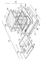
図9において、インクジェット装置16は、インクジェットヘッド22を備えたヘッドユニット26と、インクジェットヘッド22の位置を制御するヘッド位置制御装置17と、マザー基板12の位置を制御する基板位置制御装置18と、インクジェットヘッド22をマザー基板12に対して主走査移動させる主走査駆動装置19と、インクジェットヘッド22をマザー基板12に対して副走査移動させる副走査駆動装置21と、マザー基板12をインクジェット装置16内の所定の作業位置へ供給する基板供給装置23と、そしてインクジェット装置16の全般の制御を司るコントロール装置24とを有する。
【0071】
ヘッド位置制御装置17、基板位置制御装置18、主走査駆動装置19、そして副走査駆動装置21の各装置はベース9の上に設置される。また、それらの各装置は必要に応じてカバー14によって覆われる。
【0072】
インクジェットヘッド22は、例えば図2に示すように、複数、本実施形態では6個のヘッド部20と、それらのヘッド部20を並べて支持する支持手段としてのキャリッジ25とを有する。キャリッジ25は、ヘッド部20を支持すべき位置にヘッド部20よりも少し大きい穴すなわち凹部を有し、各ヘッド部20はそれらの穴の中に入れられ、さらにネジ、接着剤その他の締結手段によって固定される。また、キャリッジ25に対するヘッド部20の位置が正確に決められる場合には、特別な締結手段を用いることなく、単なる圧入によってヘッド部20を固定しても良い。
【0073】
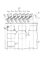
ヘッド部20は、例えば図11に示すように、複数のノズル27を列状に並べることによって形成されたノズル列28を有する。ノズル27の数は例えば180個であり、ノズル27の孔径は例えば28μmであり、ノズル27間のノズルピッチは例えば141μmである。図6(a)及び図6(b)においてカラーフィルタ1及びマザー基板12に対する主走査方向X及びそれに直交する副走査方向Yは図11において図示の通りに設定される。
【0074】
図2において、各ヘッド部20は、それらが有するノズル列28の延在方向K0がキャリッジ25の長手方向の中心軸線K1に対して角度θで傾斜するように、そのキャリッジ25に取り付けられている。また、インクジェットヘッド22は、図1に示すように、そのキャリッジ25の中心軸線K1が主走査方向Xと交差する方向、本実施形態では直角方向へ延びるように位置設定される。つまり、各ノズル列28は主走査方向に対して直角である副走査方向Yに対して角度θで傾斜する状態に位置設定される。
【0075】
インクジェットヘッド22はX方向へ平行移動することによりマザー基板12を主走査するが、この主走査の間にインクとしてのフィルタエレメント材料を各ヘッド部20内の複数のノズル27から選択的に吐出することにより、マザー基板12内の所定位置にフィルタエレメント材料を付着させる。また、インクジェットヘッド22は副走査方向Yへ所定距離、例えばノズル列28の副走査方向Y成分の長さの6個分の長さ若しくはそれよりも短い又はそれよりも長い長さだけ平行移動することにより、インクジェットヘッド22による主走査位置を所定の間隔でずらせることができる。
【0076】
個々のヘッド部20は、例えば、図13(a)及び図13(b)に示す内部構造を有する。具体的には、ヘッド部20は、例えばステンレス製のノズルプレート29と、それに対向する振動板31と、それらを互いに接合する複数の仕切部材32とを有する。ノズルプレート29と振動板31との間には、仕切部材32によって複数のインク室33と液溜り34とが形成される。複数のインク室33と液溜り34とは通路38を介して互いに連通している。
【0077】
振動板31の適所にはインク供給孔36が形成され、このインク供給孔36にインク供給装置37が接続される。このインク供給装置37はR,G,Bのうちの1色、例えばR色のフィルタエレメント材料Mをインク供給孔36へ供給する。供給されたフィルタエレメント材料Mは液溜り34に充満し、さらに通路38を通ってインク室33に充満する。
【0078】
ノズルプレート29には、インク室33からフィルタエレメント材料Mをジェット状に噴射するためのノズル27が設けられている。また、振動板31のインク室33を形成する面の裏面には、該インク室33に対応させてインク加圧体39が取り付けられている。このインク加圧体39は、図13(b)に示すように、圧電素子41並びにこれを挟持する一対の電極42a及び42bを有する。圧電素子41は電極42a及び42bへの通電によって矢印Cで示す外側へ突出するように撓み変形し、これによりインク室33の容積が増大する。すると、増大した容積分に相当するフィルタエレメント材料Mが液溜り34から通路38を通ってインク室33へ流入する。
【0079】
次に、圧電素子41への通電を解除すると、該圧電素子41と振動板31は共に元の形状へ戻る。これにより、インク室33も元の容積に戻るためインク室33の内部にあるフィルタエレメント材料Mの圧力が上昇し、ノズル27からマザー基板12(図6(b)参照)へ向けてフィルタエレメント材料Mが液滴8となって噴出する。なお、ノズル27の周辺部には、液滴8の飛行曲がりやノズル27の孔詰まり等を防止するために、例えばNi−テトラフルオロエチレン共析メッキ層から成る撥インク層43が設けられる。
【0080】
図10において、ヘッド位置制御装置17は、インクジェットヘッド22を面内回転させるαモータ44と、インクジェットヘッド22を副走査方向Yと平行な軸線回りに揺動回転させるβモータ46と、インクジェットヘッド22を主走査方向Xと平行な軸線回りに揺動回転させるγモータ47と、そしてインクジェットヘッド22を上下方向へ平行移動させるZモータ48とを有する。
【0081】
図9に示した基板位置制御装置18は、図10において、マザー基板12を載せるテーブル49と、そのテーブル49を矢印θのように面内回転させるθモータ51とを有する。また、図9に示した主走査駆動装置19は、図10に示すように、主走査方向Xへ延びるガイドレール52と、パルス駆動されるリニアモータを内蔵したスライダ53とを有する。スライダ53は内蔵するリニアモータが作動するときにガイドレール52に沿って主走査方向へ平行移動する。
【0082】
また、図9に示した副走査駆動装置21は、図10に示すように、副走査方向Yへ延びるガイドレール54と、パルス駆動されるリニアモータを内蔵したスライダ56とを有する。スライダ56は内蔵するリニアモータが作動するときにガイドレール54に沿って副走査方向Yへ平行移動する。
【0083】
スライダ53やスライダ56内においてパルス駆動されるリニアモータは、該モータに供給するパルス信号によって出力軸の回転角度制御を精細に行うことができ、従って、スライダ53に支持されたインクジェットヘッド22の主走査方向X上の位置やテーブル49の副走査方向Y上の位置等を高精細に制御できる。なお、インクジェットヘッド22やテーブル49の位置制御はパルスモータを用いた位置制御に限られず、サーボモータを用いたフィードバック制御や、その他任意の制御方法によって実現することもできる。
【0084】
図9に示した基板供給装置23は、マザー基板12を収容する基板収容部57と、マザー基板12を搬送するロボット58とを有する。ロボット58は、床、地面等といった設置面に置かれる基台59と、基台59に対して昇降移動する昇降軸61と、昇降軸61を中心として回転する第1アーム62と、第1アーム62に対して回転する第2アーム63と、第2アーム63の先端下面に設けられた吸着パッド64とを有する。吸着パッド64は空気吸引等によってマザー基板12を吸着できる。
【0085】
図9において、主走査駆動装置19によって駆動されて主走査移動するインクジェットヘッド22の軌跡下であって副走査駆動装置21の一方の脇位置に、キャッピング装置76及びクリーニング装置77が配設される。また、他方の脇位置に電子天秤78が配設される。クリーニング装置77はインクジェットヘッド22を洗浄するための装置である。電子天秤78はインクジェットヘッド22内の個々のノズル27(図11参照)から吐出されるインクの液滴の重量をノズルごとに測定する機器である。そして、キャッピング装置76はインクジェットヘッド22が待機状態にあるときにノズル27の乾燥を防止するための装置である。
【0086】
インクジェットヘッド22の近傍には、そのインクジェットヘッド22と一体に移動する関係でヘッド用カメラ81が配設される。また、ベース9上に設けた支持装置(図示せず)に支持された基板用カメラ82がマザー基板12を撮影できる位置に配置される。
【0087】
図9に示したコントロール装置24は、プロセッサを収容したコンピュータ本体部66と、入力装置としてのキーボード67と、表示装置としてのCRT(Cathode Ray Tube)ディスプレイ68とを有する。上記プロセッサは、図14に示すように、演算処理を行うCPU(Central Processing Unit)69と、各種情報を記憶するメモリすなわち情報記憶媒体71とを有する。
【0088】
図9に示したヘッド位置制御装置17、基板位置制御装置18、主走査駆動装置19、副走査駆動装置21、そして、インクジェットヘッド22内の圧電素子41(図13(b)参照)を駆動するヘッド駆動回路72の各機器は、図14において、入出力インターフェース73及びバス74を介してCPU69に接続される。また、基板供給装置23、入力装置67、ディスプレイ68、電子天秤78、クリーニング装置77及びキャッピング装置76の各機器も入出力インターフェース73及びバス74を介してCPU69に接続される。
【0089】
メモリ71は、RAM(Random Access Memory)、ROM(Read Only Memory)等といった半導体メモリや、ハードディスク、CD−ROM読取り装置、ディスク型記憶媒体等といった外部記憶装置等を含む概念であり、機能的には、インクジェット装置16の動作の制御手順が記述されたプログラムソフトを記憶する記憶領域や、図8に示す各種のR,G,B配列を実現するためのR,G,Bのうちの1色のマザー基板12(図6参照)内における吐出位置を座標データとして記憶するための記憶領域や、図10における副走査方向Yへのマザー基板12の副走査移動量を記憶するための記憶領域や、CPU69のためのワークエリアやテンポラリファイル等として機能する領域や、その他各種の記憶領域が設定される。
【0090】
CPU69は、メモリ71内に記憶されたプログラムソフトに従って、マザー基板12の表面の所定位置にインク、すなわちフィルタエレメント材料を吐出するための制御を行うものであり、具体的な機能実現部として、クリーニング処理を実現するための演算を行うクリーニング演算部と、キャッピング処理を実現するためのキャッピング演算部と、電子天秤78(図9参照)を用いた重量測定を実現するための演算を行う重量測定演算部と、インクジェットによってフィルタエレメント材料を描画するための演算を行う描画演算部とを有する。
【0091】
描画演算部を詳しく分割すれば、インクジェットヘッド22を描画のための初期位置へセットするための描画開始位置演算部と、インクジェットヘッド22を主走査方向Xへ所定の速度で走査移動させるための制御を演算する主走査制御演算部と、マザー基板12を副走査方向Yへ所定の副走査量だけずらせるための制御を演算する副走査制御演算部と、そして、インクジェットヘッド22内の複数のノズル27のうちのいずれを作動させてインクすなわちフィルタエレメント材料を吐出するかを制御するための演算を行うノズル吐出制御演算部等といった各種の機能演算部を有する。
【0092】
なお、本実施形態では、上記の各機能をCPU69を用いてソフト的に実現することにしたが、上記の各機能がCPUを用いない単独の電子回路によって実現できる場合には、そのような電子回路を用いることも可能である。
【0093】
以下、上記構成から成るインクジェット装置16の動作を図15に示すフローチャートに基づいて説明する。
【0094】
オペレータによる電源投入によってインクジェット装置16が作動すると、まず、ステップS1において初期設定が実行される。具体的には、ヘッドユニット26や基板供給装置23やコントロール装置24等が予め決められた初期状態にセットされる。
【0095】
次に、重量測定タイミングが到来すれば(ステップS2でYES)、図10のヘッドユニット26を主走査駆動装置19によって図9の電子天秤78の所まで移動させて(ステップS3)、ノズル27から吐出されるインクの量を電子天秤78を用いて測定する(ステップS4)。そして、個々のノズル27のインク吐出特性に合わせて、各ノズル27に対応する圧電素子41に印加する電圧を調節する(ステップS5)。
【0096】
次に、クリーニングタイミングが到来すれば(ステップS6でYES)、ヘッドユニット26を主走査駆動装置19によってクリーニング装置77の所まで移動させて(ステップS7)、そのクリーニング装置77によってインクジェットヘッド22をクリーニングする(ステップS8)。
【0097】
重量測定タイミングやクリーニングタイミングが到来しない場合(ステップS2及びS6でNO)、あるいはそれらの処理が終了した場合には、ステップS9において、図9の基板供給装置23を作動させてマザー基板12をテーブル49へ供給する。具体的には、基板収容部57内のマザー基板12を吸着パッド64によって吸引保持し、次に、昇降軸61、第1アーム62及び第2アーム63を移動させてマザー基板12をテーブル49まで搬送し、さらにテーブル49の適所に予め設けてある位置決めピン50(図10参照)に押し付ける。なお、テーブル49上におけるマザー基板12の位置ズレを防止するため、空気吸引等の手段によってマザー基板12をテーブル49に固定することが望ましい。
【0098】
次に、図9の基板用カメラ82によってマザー基板12を観察しながら、図10のθモータ51の出力軸を微小角度単位で回転させることによりテーブル49を微小角度単位で面内回転させてマザー基板12を位置決めする(ステップS10)。次に、図9のヘッド用カメラ81によってマザー基板12を観察しながらインクジェットヘッド22によって描画を開始する位置を演算によって決定し(ステップS11)、そして、主走査駆動装置19及び副走査駆動装置21を適宜に作動させてインクジェットヘッド22を描画開始位置へ移動する(ステップS12)。
【0099】
このとき、インクジェットヘッド22は、図1に示すように、そのキャリッジ25の中心軸線K1が主走査方向Xと直角の方向となるようにセットされる。このため、ノズル列28がインクジェットヘッド22の副走査方向Yに対して角度θで傾斜するように配設される。これは、通常のインクジェット装置の場合には、隣り合うノズル27の間の間隔であるノズル間ピッチと、隣り合うフィルタエレメント3すなわちフィルタエレメント形成領域7の間の間隔であるエレメントピッチとが異なることが多く、インクジェットヘッド22を主走査方向Xへ移動させるときに、ノズル間ピッチの副走査方向Yの寸法成分がエレメントピッチと幾何学的に等しくなるようにするための措置である。
【0100】
図15のステップS12でインクジェットヘッド22が描画開始位置に置かれると、その後、図15のステップS13でX方向への主走査が開始され、同時にインクの吐出が開始される。具体的には、図10の主走査駆動装置19が作動してインクジェットヘッド22が図1の主走査方向Xへ一定の速度で直線的に走査移動し、その移動中、インクを供給すべきフィルタエレメント形成領域7に対応するノズル27が到達したときにそのノズル27からインクすなわちフィルタエレメント材料が吐出されて該領域7が埋められてフィルタエレメント3が形成される。
【0101】
インクジェットヘッド22は、マザー基板12に対する1回の主走査が終了すると(ステップS14でYES)、反転移動して初期位置へ復帰する(ステップS15)。そしてさらに、インクジェットヘッド22は、副走査駆動装置21によって駆動されて副走査方向Yへ予め決められた副走査量、例えば6個のノズル列28の合計の長さの副走査方向Y成分だけ移動する(ステップS16)。そして次に、主走査及びインク吐出が繰り返して行われてフィルタエレメント形成領域7がフィルタエレメント材料によって埋められてフィルタエレメント3が形成される(ステップS13)。
【0102】
以上のようなインクジェットヘッド22によるフィルタエレメント3の描画作業がマザー基板12の全領域に対して完了すると(ステップS17でYES)、ステップS18でマザー基板12を基板供給装置23によって、又は別の搬送機器によって、処理後のマザー基板12が外部へ排出される。その後、オペレータによって処理終了の指示がなされない限り(ステップS1でNO)、ステップS2へ戻って別のマザー基板12に対するR,G,Bのうちの1色に関するインク吐着作業を繰り返して行う。
【0103】
オペレータから作業終了の指示があると(ステップS19でYES)、CPU69は図9においてインクジェットヘッド22をキャッピング装置76の所まで搬送して、そのキャッピング装置76によってインクジェットヘッド22に対してキャッピング処理を施す(ステップS20)。
【0104】
以上により、カラーフィルタを構成するR,G,B3色のうちの第1色、例えばR色についてのパターニングが終了し、その後、マザー基板12をR,G,Bの第2色、例えばG色をフィルタエレメント材料とするインクジェット装置16へ搬送してG色のパターニングを行い、さらに最終的にR,G,Bの第3色、例えばB色をフィルタエレメント材料とするインクジェット装置16へ搬送してB色のパターニングを行う。これにより、ストライプ配列等といった希望のR,G,Bのドット配列を有するカラーフィルタ1(図6(a))が複数個形成されたマザー基板12が製造される。このマザー基板12をカラーフィルタ領域11ごとに切断することにより、1個のカラーフィルタ1が複数個切り出される。
【0105】
なお、本カラーフィルタ1を液晶装置のカラー表示のために用いるものとすれば、本カラーフィルタ1の表面にはさらに電極や配向膜等がさらに積層されることになる。そのような場合、電極や配向膜等を積層する前にマザー基板12を切断して個々のカラーフィルタ1を切り出してしまうと、その後の電極等の形成工程が非常に面倒になる。よって、そのような場合には、マザー基板12上でカラーフィルタ1が完成した後に、直ぐにマザー基板12を切断してしまうのではなく、電極形成や配向膜形成等といった必要な付加工程が終了した後にマザー基板12を切断することが望ましい。
【0106】
以上のように本実施形態に係るカラーフィルタの製造方法及び製造装置によれば、図1に示すように、複数のヘッド部20を支持した支持手段としてのキャリッジ25によって基板12を主走査する間にそれら複数のヘッド部20のノズル列28からインクを吐出するので、1個のヘッド部だけを用いて基板12の表面を走査する場合に比べて走査時間を短縮でき、従って、カラーフィルタの製造時間を短縮できる。
【0107】
また、各ヘッド部20は副走査方向Yに対して角度θの傾斜状態で主走査を行うので、各ヘッド部20に属する複数のノズル27のノズル間ピッチを基板12上のフィルタエレメント形成領域7の間の間隔、すなわちエレメント間ピッチに一致させることができる。このようにノズル間ピッチとエレメント間ピッチとを幾何学的に一致させれば、ノズル列28を副走査方向Yに関して位置制御する必要がなくなるので好都合である。
【0108】
なお、本実施形態ではヘッド部20がキャリッジ25に固定されるので、傾斜角度θは1個のキャリッジ25に対して1種類である。従って、基板12側のエレメント間ピッチが変化する場合には、そのエレメント間ピッチに対応した傾斜角度θを実現できる他のキャリッジ25を用いる必要がある。
【0109】
さらに、本実施形態では、キャリッジ25の全体を傾斜させるのではなくて個々のヘッド部20を傾斜させるので、基板12に近い側のノズル27と基板12から遠い側のノズル27までの距離Tはキャリッジ25の全体を傾斜させる場合に比べて著しく小さくなり、それ故、インクジェットヘッド22によって基板12を走査する時間を著しく短縮できる。これにより、カラーフィルタの製造時間を短縮できる。
【0110】
なお、本実施形態の製造装置及び製造方法では、インクジェットヘッド22を用いたインク吐出によってフィルタエレメント3を形成するので、フォトリソグラフィー法を用いる方法のような複雑な工程を経る必要も無く、また、材料を浪費することも無い。
【0111】
本第1実施形態においては、隔壁6として透光性のない樹脂材料を用いたが、隔壁6として透光性の樹脂材料を用いることも、もちろん可能である。その場合にあっては、フィルタエレメント間に対応する位置、例えば隔壁6の上、隔壁6の下等に別途、遮光性の金属膜又は樹脂材料を設けてブラックマスクとしても良い。また、透光性の樹脂材料で隔壁6を形成し、ブラックマスクを設けない構成としても良い。
【0112】
また、本第1実施形態においては、フィルタエレメントとしてR,G,Bを用いたが、R,G,Bに限定されることはなく、例えばC(シアン)、M(マゼンタ)、Y(イエロー)を採用してもかまわない。その場合にあっては、R,G,Bのフィルタエレメント材料に代えて、C,M,Yの色を有するフィルタエレメント材料を用いれば良い。
【0113】
(第2実施形態)
図3は、本発明に係るカラーフィルタの製造方法及び製造装置の他の実施形態によってインクジェットヘッド22を用いてマザー基板12内のカラーフィルタ形成領域11内の各フィルタエレメント形成領域7へインクすなわちフィルタエレメント材料を吐出によって供給する場合を模式的に示している。
【0114】
本実施形態によって実施される概略の工程は図7に示した工程と同じであり、インク吐着のために用いるインクジェット装置も図9に示した装置と機構的には同じである。
【0115】
本実施形態が図1に示した先の実施形態と異なる点は、キャリッジ25によるヘッド部20の支持構造に改変を加えたことである。具体的には、図4において、個々のヘッド部20をキャリッジ25に対してヘッド部20の中心軸線K2を中心として矢印Nのように回転可能、すなわち面内回転可能に支持する。また、個々のヘッド部20をキャリッジ25に対して矢印Pで示すようにスライド移動、すなわち面内平行移動可能に支持する。また、キャリッジ25にノズル列角度制御装置83及びノズル列間隔制御装置84を付設する。
【0116】
ノズル列角度制御装置83は、複数のノズル列28の面内傾斜角度θを個別に又は一括に制御するものである。このノズル列角度制御装置83は任意の構造によって構成できるが、例えば、ケーシング25に矢印Nのように面内回転可能に取り付けられたヘッド部20をパルスモータやサーボモータ等といった回転角度制御が可能な動力源に直接に又は動力伝達機構等を介して間接に接続することによって構成できる。この構成によれば、上記動力源の出力角度値を制御することによって各ノズル列20の傾斜角度θを希望の値に調節でき、さらにその調節後の上記動力源の出力軸をロック状態に保持することにより各ノズル列20の傾斜角度θを希望の値に固定保持できる。
【0117】
また、ノズル列間隔制御装置84は、複数のノズル列20の間隔を個々の間隔ごとに個別に又は一括に制御するものである。このノズル列間隔制御装置84は任意の構造によって構成できるが、例えば、矢印Pのようにケーシング25にスライド移動可能に取り付けられたヘッド部20をパルスモータやサーボモータ等といった回転角度制御が可能な回転機器を動力源とするスライド駆動装置や、リニアモータ等といった直動駆動源を用いて構成されるスライド駆動装置等に接続することによって構成できる。
【0118】
本実施形態によれば、図4のノズル列角度制御装置83を作動させて図3においてヘッド部20を矢印Nのように面内回転させることにより、ヘッド部20の面内傾斜角度θを調節して、ノズル列28のノズル間ピッチを基板12上のフィルタエレメント形成領域7のエレメント間ピッチに一致させる。そしてさらに、図4のノズル列間隔制御装置84を作動させて図3においてヘッド部20の間の間隔を調節して、互いに隣り合うノズル列28の端部同士のノズル間距離を基板12側のエレメント間ピッチに一致させる。
【0119】
以上により、6個のノズル列28をエレメント間ピッチに一致するノズル間ピッチを有する連続した長いノズル列に形成することができる。このように、本実施形態によれば、1個のインクジェットヘッド22内のノズル間ピッチを適宜に調節することにより、エレメント間ピッチの異なるパターンを基板12上に描画できる。
【0120】
(第3実施形態)
図5は、本発明に係るカラーフィルタの製造装置及び製造方法の他の実施形態によってインクジェットヘッド22を用いてマザー基板12内のカラーフィルタ形成領域11内の各フィルタエレメント形成領域7へインクすなわちフィルタエレメント材料を吐出によって供給する場合を模式的に示している。
【0121】
本実施形態によって実施される概略の工程は図7に示した工程と同じであり、インク吐着のために用いるインクジェット装置も図9に示した装置と機構的には同じである。
【0122】
本実施形態が図1及び図3に示した先の実施形態と異なる点は、ノズル列28の傾斜角度θが各ノズル列28間で大きさは同じであるが傾斜方向がプラス・マイナス間で交互に変化することである。この方法によっても、6個のノズル列28を基板12側のエレメント間ピッチに一致するノズル間ピッチを有する連続した長いノズル列に形成することができる。
【0123】
なお、本実施形態に関しても、図1に示したようにノズル列28が固定される構造にすることもできるし、あるいは、図3に示したようにノズル列28の傾斜角度θ及びノズル列間距離が調節可能な構造にすることもできる。
【0124】
(第4実施形態)
図12は、本発明で用いるヘッド部20の改変例を示している。ここに示すヘッド部20が図11に示したヘッド部20と異なる点は、ノズル列28を主走査方向Xに沿って2列設けたことである。これにより、同じ主走査ラインに載った2つのノズル27によって1つのフィルタエレメント形成領域7にフィルタエレメント材料を供給することができる。
【0125】
なお、本実施形態においてインクジェットヘッド22の中心軸線K0は副走査方向Yに対して面内傾斜角度θで傾斜しているので、2段のノズル列28内のノズル27はキャリッジ25の中心軸線K0に直角の方向に並ぶのではなく、主走査方向Xに載るようにキャリッジ25から見れば互いにずれて配列されることが望ましい。
【0126】
(第5実施形態)
図16は、本発明で用いるヘッド部20のさらに他の改変例を示している。このヘッド部20が図11に示すヘッド部20と異なる点は、R色インクを吐出するノズル列28Rと、G色インクを吐出するノズル列28Gと、B色インクを吐出するノズル列28Bといった3種類のノズル列を1個のヘッド部20に形成し、それら3種類のそれぞれに図13(a)及び図13(b)に示したインク吐出系を設け、R色ノズル列28Rに対応するインク吐出系にはRインク供給装置37Rを接続し、G色ノズル列28Gに対応するインク吐出系にはGインク供給装置37Gを接続し、そしてB色ノズル列28Bに対応するインク吐出系にはBインク供給装置37Bを接続したことである。
【0127】
本実施形態によって実施される概略の工程は図7に示した工程と同じであり、インク吐着のために用いるインクジェット装置も基本的には図9に示した装置と同じである。
【0128】
図11に示した実施形態では、ヘッド部20に1種類のノズル列28が設けられるだけであったので、R,G,B3色によってカラーフィルタを形成する際には図2等に示したインクジェットヘッド22がR,G,Bの3色それぞれについて準備されていなければならなかった。これに対し、図16に示す構造のヘッド部20を使用する場合には、複数個のヘッド部20を備えたインクジェットヘッド22のX方向への1回の主走査によってR,G,Bの3色を同時にマザー基板12へ付着させることができるので、インクジェットヘッド22は1つだけ準備しておけば足りる。
【0129】
(第6実施形態)
図17は、本発明に係る液晶装置の製造装置を用いた製造方法の一実施形態を示している。また、図18はその製造方法によって製造される液晶装置の一実施形態を示している。また、図19は図18におけるX−X線に従った液晶装置の断面構造を示している。液晶装置の製造方法及び製造装置の説明に先立って、まず、その製造方法によって製造される液晶装置をその一例を挙げて説明する。なお、本実施形態の液晶装置は、単純マトリクス方式でフルカラー表示を行う半透過反射方式の液晶装置である。
【0130】
図18において、液晶装置101は、液晶パネル102に半導体チップとしての液晶駆動用IC103a及び103bを実装し、配線接続要素としてのFPC(Flexible Printed Circuit)104を液晶パネル102に接続し、さらに液晶パネル102の裏面側に照明装置106をバックライトとして設けることによって形成される。
【0131】
液晶パネル102は、第1基板107aと第2基板107bとをシール材108によって貼り合わせることによって形成される。シール材108は、例えば、スクリーン印刷等によってエポキシ系樹脂を第1基板107a又は第2基板107bの内側表面に環状に付着させることによって形成される。また、シール材108の内部には図19に示すように、導電性材料によって球状又は円筒状に形成された導通材109が分散状態で含まれる。
【0132】
図19において、第1基板107aは透明なガラスや、透明なプラスチック等によって形成された板状の基材111aを有する。この基材111aの内側表面(図19の上側表面)には反射膜112が形成され、その上に絶縁膜113が積層され、その上に第1電極114aが矢印D方向から見てストライプ状(図18参照)に形成され、さらにその上に配向膜116aが形成される。また、基材111aの外側表面(図19の下側表面)には偏光板117aが貼着等によって装着される。
【0133】
図18では第1電極114aの配列を分かり易く示すために、それらのストライプ間隔を実際よりも大幅に広く描いており、よって、第1電極114aの本数が少なく描かれているが、実際には、第1電極114aはより多数本が基材111a上に形成される。
【0134】
図19において、第2基板107bは透明なガラスや、透明なプラスチック等によって形成された板状の基材111bを有する。この基材111bの内側表面(図19の下側表面)にはカラーフィルタ118が形成され、その上に第2電極114bが上記第1電極114aと直交する方向へ矢印D方向から見てストライプ状(図18参照)に形成され、さらにその上に配向膜116bが形成される。また、基材111bの外側表面(図19の上側表面)には偏光板117bが貼着等によって装着される。
【0135】
図18では、第2電極114bの配列を分かりやすく示すために、第1電極114aの場合と同様に、それらのストライプ間隔を実際よりも大幅に広く描いており、よって、第2電極114bの本数が少なく描かれているが、実際には、第2電極114bはより多数本が基材111b上に形成される。
【0136】
図19において、第1基板107a、第2基板107b及びシール材108によって囲まれる間隙、いわゆるセルギャップ内には液晶、例えばSTN(Super Twisted Nematic)液晶Lが封入されている。第1基板107a又は第2基板107bの内側表面には微小で球形のスペーサ119が多数分散され、これらのスペーサ119がセルギャップ内に存在することによりそのセルギャップの厚さが均一に維持される。
【0137】
第1電極114aと第2電極114bは互いに直交関係に配置され、それらの交差点は図19の矢印D方向から見てドット・マトリクス状に配列する。そして、そのドット・マトリクス状の各交差点が1つの絵素ピクセルを構成する。カラーフィルタ118は、R(赤)、G(緑)、B(青)の各色要素を矢印D方向から見て所定のパターン、例えば、ストライプ配列、デルタ配列、モザイク配列等のパターンで配列させることによって形成されている。上記の1つの絵素ピクセルはそれらR,G,Bの各1つずつに対応しており、そしてR,G,Bの3色絵素ピクセルが1つのユニットになって1画素が構成される。
【0138】
ドット・マトリクス状に配列される複数の絵素ピクセル、従って画素、を選択的に発光させることにより、液晶パネル102の第2基板107bの外側に文字、数字等といった像が表示される。このようにして像が表示される領域が有効画素領域であり、図18及び図19において矢印Vによって示される平面的な矩形領域が有効表示領域となっている。
【0139】
図19において、反射膜112はAPC合金、Al(アルミニウム)等といった光反射性材料によって形成され、第1電極114aと第2電極114bとの交差点である各絵素ピクセルに対応する位置に開口121が形成されている。結果的に、開口121は図19の矢印D方向から見て、絵素ピクセルと同じドット・マトリクス状に配列されている。
【0140】
第1電極114a及び第2電極114bは、例えば、透明導電材であるITOによって形成される。また、配向膜116a及び116bは、ポリイミド系樹脂を一様な厚さの膜状に付着させることによって形成される。これらの配向膜116a及び116bがラビング処理を受けることにより、第1基板107a及び第2基板107bの表面上における液晶分子の初期配向が決定される。
【0141】
図18において、第1基板107aは第2基板107bよりも広い面積に形成されており、これらの基板をシール材108によって貼り合わせたとき、第1基板107aは第2基板107bの外側へ張り出す基板張出し部107cを有する。そして、この基板張出し部107cには、第1電極114aから延び出る引出し配線114c、シール材108の内部に存在する導通材109(図19参照)を介して第2基板107b上の第2電極114bと導通する引出し配線114d、液晶駆動用IC103aの入力用バンプ、すなわち入力用端子に接続される金属配線114e、そして液晶駆動用IC103bの入力用バンプに接続される金属配線114f等といった各種の配線が適切なパターンで形成される。
【0142】
本実施形態では、第1電極114aから延びる引出し配線114c及び第2電極114bに導通する引出し配線114dはそれらの電極と同じ材料であるITO、すなわち導電性酸化物によって形成される。また、液晶駆動用IC103a及び103bの入力側の配線である金属配線114e及び114fは電気抵抗値の低い金属材料、例えばAPC合金によって形成される。APC合金は、主としてAgを含み、付随してPd及びCuを含む合金、例えば、Ag98%、Pd1%、Cu1%から成る合金である。
【0143】
液晶駆動用IC103a及び液晶駆動用IC103bは、ACF(Anisotropic Conductive Film:異方性導電膜)122によって基板張出し部107cの表面に接着されて実装される。すなわち、本実施形態では基板上に半導体チップが直接に実装される構造の、いわゆるCOG(Chip On Glass)方式の液晶パネルとして形成されている。このCOG方式の実装構造においては、ACF122の内部に含まれる導電粒子によって、液晶駆動用IC103a及び103bの入力側バンプと金属配線114e及び114fとが導電接続され、液晶駆動用IC103a及び103bの出力側バンプと引出し配線114c及び114dとが導電接続される。
【0144】
図18において、FPC104は、可撓性の樹脂フィルム123と、チップ部品124を含んで構成された回路126と、金属配線端子127とを有する。回路126は樹脂フィルム123の表面に半田付けその他の導電接続手法によって直接に搭載される。また、金属配線端子127はAPC合金、Cr、Cuその他の導電材料によって形成される。FPC104のうち金属配線端子127が形成された部分は、第1基板107aのうち金属配線114e及び金属配線114fが形成された部分にACF122によって接続される。そして、ACF122の内部に含まれる導電粒子の働きにより、基板側の金属配線114e及び114fとFPC側の金属配線端子127とが導通する。
【0145】
FPC104の反対側の辺端部には外部接続端子131が形成され、この外部接続端子131が図示しない外部回路に接続される。そして、この外部回路から伝送される信号に基づいて液晶駆動用IC103a及び103bが駆動され、第1電極114a及び第2電極114bの一方に走査信号が供給され、他方にデータ信号が供給される。これにより、有効表示領域V内に配列されたドット・マトリクス状の絵素ピクセルが個々のピクセルごとに電圧制御され、その結果、液晶Lの配向が個々の絵素ピクセルごとに制御される。
【0146】
図18において、いわゆるバックライトとして機能する照明装置106は、図19に示すように、アクリル樹脂等によって構成された導光体132と、その導光体132の光出射面132bに設けられた拡散シート133と、導光体132の光出射面132bの反対面に設けられた反射シート134と、発光源としてのLED(Light Emitting Diode)136とを有する。
【0147】
LED136はLED基板137に支持され、そのLED基板137は、例えば導光体132と一体に形成された支持部(図示せず)に装着される。LED基板137が支持部の所定位置に装着されることにより、LED136が導光体132の側辺端面である光取込み面132aに対向する位置に置かれる。なお、符号138は液晶パネル102に加わる衝撃を緩衝するための緩衝材を示している。
【0148】
LED136が発光すると、その光は光取込み面132aから取り込まれて導光体132の内部へ導かれ、反射シート134や導光体132の壁面で反射しながら伝播する間に光出射面132bから拡散シート133を通して外部へ平面光として出射する。
【0149】
本実施形態の液晶装置101は以上のように構成されているので、太陽光、室内光等といった外部光が十分に明るい場合には、図19において、第2基板107b側から外部光が液晶パネル102の内部へ取り込まれ、その光が液晶Lを通過した後に反射膜112で反射して再び液晶Lへ供給される。液晶Lはこれを挟持する電極114a及び114bによってR,G,Bの絵素ピクセルごとに配向制御されており、よって、液晶Lへ供給された光は絵素ピクセルごとに変調され、その変調によって偏光板117bを通過する光と、通過できない光とによって液晶パネル102の外部に文字、数字等といった像が表示される。これにより、反射型の表示が行われる。
【0150】
他方、外部光の光量が十分に得られない場合には、LED136が発光して導光体132の光出射面132bから平面光が出射され、その光が反射膜112に形成された開口121を通して液晶Lへ供給される。このとき、反射型の表示と同様にして、供給された光が配向制御される液晶Lによって絵素ピクセルごとに変調され、これにより、外部へ像が表示される。これにより、透過型の表示が行われる。
【0151】
上記構成の液晶装置101は、例えば、図17に示す製造方法によって製造される。この製造方法において、工程P1〜工程P6の一連の工程が第1基板107aを形成する工程であり、工程P11〜工程P14の一連の工程が第2基板107bを形成する工程である。第1基板形成工程と第2基板形成工程は、通常、それぞれが独自に行われる。
【0152】
まず、第1基板形成工程について説明すれば、透光性ガラス、透光性プラスチック等によって形成された大面積のマザー原料基材の表面に液晶パネル102の複数個分の反射膜112をフォトリソグラフィー法等を用いて形成し、さらにその上に絶縁膜113を周知の成膜法を用いて形成し(工程P1)、次に、フォトリソグラフィー法等を用いて第1電極114a及び配線114c,114d,114e,114fを形成する(工程P2)。
【0153】
次に、第1電極114aの上に塗布、印刷等によって配向膜116aを形成し(工程P3)、さらにその配向膜116aに対してラビング処理を施すことにより液晶の初期配向を決定する(工程P4)。次に、例えばスクリーン印刷等によってシール材108を環状に形成し(工程P5)、さらにその上に球状のスペーサ119を分散する(工程P6)。以上により、液晶パネル102の第1基板107a上のパネルパターンを複数個分有する大面積のマザー第1基板が形成される。
【0154】
以上の第1基板形成工程とは別に、第2基板形成工程(図17の工程P11〜工程P14)を実施する。まず、透光性ガラス、透光性プラスチック等によって形成された大面積のマザー原料基材を用意し、その表面に液晶パネル102の複数個分のカラーフィルタ118を形成する(工程P11)。このカラーフィルタの形成工程は図7に示した製造方法を用いて行われ、その製造方法中のR,G,Bの各色フィルタエレメントの形成は図9のインクジェット装置16を用いて図1、図2、図3、図4、図5等に示したインクジェットヘッドの制御方法に従って実行される。これらカラーフィルタの製造方法及びインクジェットヘッドの制御方法は既に説明した内容と同じであるので、それらの説明は省略する。
【0155】
図7(d)に示すようにマザー基板12すなわちマザー原料基材の上にカラーフィルタ1すなわちカラーフィルタ118が形成されると、次に、フォトリソグラフィー法によって第2電極114bが形成され(工程P12)、さらに塗布、印刷等によって配向膜116bが形成され(工程P13)、さらにその配向膜116bに対してラビング処理が施されて液晶の初期配向が決められる(工程P14)。以上により、液晶パネル102の第2基板107b上のパネルパターンを複数個分有する大面積のマザー第2基板が形成される。
【0156】
以上により大面積のマザー第1基板及びマザー第2基板が形成された後、それらのマザー基板をシール材108を間に挟んでアライメント、すなわち位置合わせした上で互いに貼り合わせる(工程P21)。これにより、液晶パネル複数個分のパネル部分を含んでいて未だ液晶が封入されていない状態の空のパネル構造体が形成される。
【0157】
次に、完成した空のパネル構造体の所定位置にスクライブ溝、すなわち切断用溝を形成し、さらにそのスクライブ溝を基準にしてパネル構造体をブレイク、すなわち切断する(工程P22)。これにより、各液晶パネル部分のシール材108の液晶注入用開口110(図18参照)が外部へ露出する状態の、いわゆる短冊状の空のパネル構造体が形成される。
【0158】
その後、露出した液晶注入用開口110を通して各液晶パネル部分の内部に液晶Lを注入し、さらに各液晶注入口110を樹脂等によって封止する(工程P23)。通常の液晶注入処理は、例えば、貯留容器の中に液晶を貯留し、その液晶が貯留された貯留容器と短冊状の空パネルをチャンバー等に入れ、そのチャンバー等を真空状態にしてからそのチャンバーの内部において液晶の中に短冊状の空パネルを浸漬し、その後、チャンバーを大気圧に開放することによって行われる。このとき、空パネルの内部は真空状態なので、大気圧によって加圧される液晶が液晶注入用開口を通してパネルの内部へ導入される。液晶注入後の液晶パネル構造体のまわりには液晶が付着するので、液晶注入処理後の短冊状パネルは工程24において洗浄処理を受ける。
【0159】
その後、液晶注入及び洗浄が終わった後の短冊状のマザーパネルに対して再び所定位置にスクライブ溝を形成し、さらにそのスクライブ溝を基準にして短冊状パネルを切断することにより、複数個の液晶パネルが個々に切り出される(工程P25)。こうして作製された個々の液晶パネル102に対して図18に示すように、液晶駆動用IC103a,103bを実装し、照明装置106をバックライトとして装着し、さらにFPC104を接続することにより、目標とする液晶装置101が完成する(工程P26)。
【0160】
以上に説明した液晶装置の製造方法及び製造装置は、特にカラーフィルタを製造する段階において次のような特徴を有する。すなわち、インクジェットヘッドとして図1、図2、図3、図4又は図5等に示した構造を採用して、複数のヘッド部20を支持した支持手段としてのキャリッジ25によって基板12を主走査する間にそれら複数のヘッド部20のノズル列28からインクを吐出するので、1個のヘッド部だけを用いて基板12の表面を走査する場合に比べて走査時間を短縮でき、従って、カラーフィルタの製造時間を短縮できる。
【0161】
また、各ヘッド部20は副走査方向Yに対して角度θの傾斜状態で主走査を行うので、各ヘッド部20に属する複数のノズル27のノズル間ピッチを基板12上のフィルタエレメント形成領域7の間の間隔、すなわちエレメント間ピッチに一致させることができる。このようにノズル間ピッチとエレメント間ピッチとを幾何学的に一致させれば、ノズル列28を副走査方向Yに関して位置制御する必要がなくなるので好都合である。
【0162】
また、キャリッジ25の全体を傾斜させるのではなくて個々のヘッド部20を傾斜させるので、基板12に近い側のノズル27と基板12から遠い側のノズル27までの距離Tはキャリッジ25の全体を傾斜させる場合に比べて著しく小さくなり、それ故、インクジェットヘッド22によって基板12を走査する時間を著しく短縮できる。これにより、カラーフィルタの製造時間を短縮できる。
【0163】
なお、本実施形態の製造装置及び製造方法では、インクジェットヘッド22を用いたインク吐出によってフィルタエレメント3を形成するので、フォトリソグラフィー法を用いる方法のような複雑な工程を経る必要も無く、また、材料を浪費することも無い。
【0164】
(第8実施形態)
図20は、本発明に係るEL装置の製造装置を用いて行われる製造方法の一実施形態を示している。また、図21はその製造方法の主要工程及び最終的に得られるEL装置の主要断面構造を示している。図21(d)に示すように、EL装置201は、透明基板204上に画素電極202を形成し、各画素電極202間にバンク205を矢印G方向から見て格子状に形成し、それらの格子状凹部の中に正孔注入層220を形成し、矢印G方向から見てストライプ配列等といった所定配列となるようにR色発光層203R、G色発光層203G及びB色発光層203Bを各格子状凹部の中に形成し、さらにそれらの上に対向電極213を形成することによって形成される。
【0165】
上記画素電極202をTFD(Thin Film Diode:薄膜ダイオード)素子等といった2端子型のアクティブ素子によって駆動する場合には、上記対向電極213は矢印G方向から見てストライプ状に形成される。また、画素電極202をTFT(Thin Film Transistor:薄膜トランジスタ)等といった3端子型のアクティブ素子によって駆動する場合には、上記対向電極213は単一な面電極として形成される。
【0166】
各画素電極202と各対向電極213とによって挟まれる領域が1つの絵素ピクセルとなり、R,G,B3色の絵素ピクセルが1つのユニットとなって1つの画素を形成する。各絵素ピクセルを流れる電流を制御することにより、複数の絵素ピクセルのうちの希望するものを選択的に発光させ、これにより、矢印H方向に希望するフルカラー像を表示することができる。
【0167】
上記EL装置201は、例えば、図20に示す製造方法によって製造される。すなわち、工程P51及び図21(a)のように、透明基板204の表面にTFD素子やTFT素子等といった能動素子を形成し、さらに画素電極202を形成する。形成方法としては、例えば、フォトリソグラフィー法、真空状着法、スパッタリング法、パイロゾル法等を用いることができる。画素電極の材料としてはITO(Indium Tin Oxide)、酸化スズ、酸化インジウムと酸化亜鉛との複合酸化物等を用いることができる。
【0168】
次に、工程P52及び図20(a)に示すように、隔壁すなわちバンク205を周知のパターニング手法、例えばフォトリソグラフィー法を用いて形成し、このバンク205によって各透明電極202の間を埋めた。これにより、コントラストの向上、発光材料の混色の防止、画素と画素との間からの光漏れ等を防止することができる。バンク205の材料としては、EL材料の溶媒に対して耐久性を有するものであれば特に限定されないが、フロロカーボンガスプラズマ処理によりフッ素樹脂化できること、例えば、アクリル樹脂、エポキシ樹脂、感光性ポリイミド等といった有機材料が好ましい。
【0169】
次に、正孔注入層用インクを塗布する直前に、基板204に酸素ガスとフロロカーボンガスプラズマの連続プラズマ処理を行った(工程P53)。これにより、ポリイミド表面は撥水化され、ITO表面は親水化され、インクジェット液滴を微細にパターニングするための基板側の濡れ性の制御ができる。プラズマを発生する装置としては、真空中でプラズマを発生する装置でも、大気中でプラズマを発生する装置でも同様に用いることができる。
【0170】
次に、工程P54及び図21(a)に示すように、正孔注入層用インクを図9のインクジェット装置16のインクジェットヘッド22から吐出し、各画素電極202の上にパターニング塗布を行った。具体的なインクジェットヘッドの制御方法は図1、図2、図3、図4又は図5に示した方法を用いた。その塗布後、真空(1torr)中、室温、20分という条件で溶媒を除去し(工程P55)、その後、大気中、20℃(ホットプレート上)、10分の熱処理により、発光層用インクと相溶しない正孔注入層220を形成した(工程P56)。膜厚は40nmであった。
【0171】
次に、工程P57及び図21(b)に示すように、各フィルタエレメント領域内の正孔注入層220の上にインクジェット手法を用いてR発光層用インク及びG発光層用インクを塗布した。ここでも、各発光層用インクは、図9のインクジェット装置16のインクジェットヘッド22から吐出し、さらにインクジェットヘッドの制御方法は図1、図2、図3、図4又は図5に示した方法に従った。インクジェット方式によれば、微細なパターニングを簡便に且つ短時間に行うことができる。また、インク組成物の固形分濃度及び吐出量を変えることにより膜厚を変えることが可能である。
【0172】
発光層用インクの塗布後、真空(1torr)中、室温、20分等という条件で溶媒を除去し(工程P58)、続けて窒素雰囲気中、150℃、4時間の熱処理により共役化させてR色発光層203R及びG色発光層203Gを形成した(工程P59)。膜厚は50nmであった。熱処理により共役化した発光層は溶媒に不溶である。
【0173】
なお、発光層を形成する前に正孔注入層220に酸素ガスとフロロカーボンガスプラズマの連続プラズマ処理を行っても良い。これにより、正孔注入層220上にフッ素化物層が形成され、イオン化ポテンシャルが高くなることにより正孔注入効率が増し、発光効率の高い有機EL装置を提供できる。
【0174】
次に、工程P60及び図21(c)に示すように、B色発光層203Bを各絵素ピクセル内のR色発光層203R、G色発光層203G及び正孔注入層220の上に重ねて形成した。これにより、R,G,Bの3原色を形成するのみならず、R色発光層203R及びG色発光層203Gとバンク205との段差を埋めて平坦化することができる。これにより、上下電極間のショートを確実に防ぐことができる。B色発光層203Bの膜厚を調整することで、B色発光層203BはR色発光層203R及びG色発光層203Gとの積層構造において、電子注入輸送層として作用してB色には発光しない。
【0175】
以上のようなB色発光層203Bの形成方法としては、例えば湿式法として一般的なスピンコート法を採用することもできるし、あるいは、R色発光層203R及びG色発光層203Gの形成法と同様のインクジェット法を採用することもできる。
【0176】
その後、工程P61及び図21(d)に示すように、対向電極213を形成することにより、目標とするEL装置201を製造した。対向電極213はそれが面電極である場合には、例えば、Mg,Ag,Al,Li等を材料として、蒸着法、スパッタ法等といった成膜法を用いて形成できる。また、対向電極213がストライプ状電極である場合には、成膜された電極層をフォトリソグラフィー法等といったパターニング手法を用いて形成できる。
【0177】
以上に説明したEL装置の製造方法及び製造装置によれば、インクジェットヘッドとして図1、図2、図3、図4又は図5等に示した構造を採用して、複数のヘッド部20を支持した支持手段としてのキャリッジ25によって基板12を主走査する間にそれら複数のヘッド部20のノズル列28からインクを吐出するので、1個のヘッド部だけを用いて基板12の表面を走査する場合に比べて走査時間を短縮でき、従って、EL装置の製造時間を短縮できる。
【0178】
また、各ヘッド部20は副走査方向Yに対して角度θの傾斜状態で主走査を行うので、各ヘッド部20に属する複数のノズル27のノズル間ピッチを基板12上のEL絵素ピクセル形成領域7の間の間隔、すなわちエレメント間ピッチに一致させることができる。このようにノズル間ピッチとエレメント間ピッチとを幾何学的に一致させれば、ノズル列28を副走査方向Yに関して位置制御する必要がなくなるので好都合である。
【0179】
また、キャリッジ25の全体を傾斜させるのではなくて個々のヘッド部20を傾斜させるので、基板12に近い側のノズル27と基板12から遠い側のノズル27までの距離Tはキャリッジ25の全体を傾斜させる場合に比べて著しく小さくなり、それ故、インクジェットヘッド22によって基板12を走査する時間を著しく短縮できる。これにより、EL装置の製造時間を短縮できる。 なお、本実施形態の製造装置及び製造方法では、インクジェットヘッド22を用いたインク吐出によって絵素ピクセル3を形成するので、フォトリソグラフィー法を用いる方法のような複雑な工程を経る必要も無く、また、材料を浪費することも無い。
【0180】
(その他の実施形態)
以上、好ましい実施形態を挙げて本発明を説明したが、本発明はその実施形態に限定されるものでなく、請求の範囲に記載した発明の範囲内で種々に改変できる。
【0181】
例えば、以上に説明した実施形態では、図1に示すようにインクジェットヘッド22の中に6個のヘッド部20を設けたが、ヘッド部20の数はより少なく又はより多くすることができる。
【0182】
また、図1等に示した実施形態では、マザー基板12の中に複数列のカラーフィルタ形成領域11が設定される場合を例示したが、マザー基板12の中に1列のカラーフィルタ形成領域11が設定される場合にも本発明を適用できる。また、マザー基板12とほぼ同じ大きさの又はそれよりもかなり小さい1個のカラーフィルタ形成領域11だけがそのマザー基板12の中に設定される場合にも本発明を適用できる。
【0183】
また、図9及び図10に示したカラーフィルタの製造装置では、インクジェットヘッド22をX方向へ移動させて基板12を主走査し、基板12を副走査駆動装置21によってY方向へ移動させることによりインクジェットヘッド22によって基板12を副走査することにしたが、これとは逆に、基板12のY方向への移動によって主走査を実行し、インクジェットヘッド22のX方向への移動によって副走査を実行することもできる。
【0184】
また、上記実施形態では、圧電素子の撓み変形を利用してインクを吐出する構造のインクジェットヘッドを用いたが、他の任意の構造のインクジェットヘッドを用いることもできる。
【0185】
また、上記実施形態では、主走査方向と副走査方向とが直交する最も一般的な構成についてのみ例示したが、主走査方向と副走査方向との関係は直交関係には限られず、任意の角度で交差していればよい。
【0186】
吐出させる材料としては、基板等の対象物上に形成する要素に応じて種々選択可能であり、例えば上述してきたインク、EL発光材料の他にも、シリカガラス前駆体、金属化合物等の導電材料、誘電体材料、又は半導体材料がその一例として挙げられる。
【0187】
また、上記実施形態では、カラーフィルタの製造方法及び製造装置、液晶装置の製造方法及び製造装置、EL装置の製造方法及び製造装置、を例として説明してきたが、本発明はこれらに限定されることなく、対象物上に微細パターニングを施す工業技術全般に用いることが可能である。
【0188】
例えば、各種半導体素子(薄膜トランジスタ、薄膜ダイオード等)、各種配線パターン、及び絶縁膜の形成等がその利用範囲の一例として挙げられる。
【0189】
ヘッドから吐出させる材料としては、基板等の対象物上に形成する要素に応じて種々選択可能であり、例えば上述してきたインク、EL発光材料の他にも、シリカガラス前駆体、金属化合物等の導電材料、誘電体材料、又は半導体材料がその一例として挙げられる。
【0190】
また、上記実施形態では、簡便のため「インクジェットヘッド」と呼称してきたが、このインクジェットヘッドから吐出される吐出物はインクには限定されず、例えば、前述のEL発光材料、シリカガラス前駆体、金属化合物等の導電性材料、誘電体材料、又は半導体材料等様々であることはいうまでもない。上記実施形態の製造方法により製造された液晶装置、EL装置は、例えば携帯電話機、携帯型コンピュータ等といった電子機器の表示部に搭載することができる。
【0191】
【発明の効果】
本発明に係るカラーフィルタ、液晶装置及びEL装置のそれぞれの製造装置並びにそれらの製造方法によれば、複数のヘッド部によって基板を主走査する間にそれら複数のヘッド部からインクを吐出することができ、それ故、1個のヘッド部を用いて基板表面を走査する場合に比べて、走査時間を短縮できる。
【0192】
また、各ヘッド部は傾斜状態で主走査を行うので、各ヘッド部に属する複数のノズルのノズル間ピッチを基板上に形成するフィルタエレメントや絵素ピクセルのエレメント間ピッチに一致させることができる。
【0193】
さらに、複数のヘッド部を支持する支持機構の全体を傾斜させるのではなくて個々のヘッド部を傾斜させるので、基板に近い側のノズルと基板から遠い側のノズルまでの距離は支持手段の全体を傾斜させる場合に比べて小さくなり、それ故、支持機構によって基板を走査する時間を短縮できる。これにより、カラーフィルタや液晶装置やEL装置等の製造時間を短縮できる。
【図面の簡単な説明】
【図1】本発明に係るカラーフィルタの製造装置の一実施形態を用いて行われる製造方法の主要工程を模式的に示す平面図である。
【図2】図1のインクジェットヘッドの斜視図である。
【図3】本発明に係るカラーフィルタの製造装置の他の実施形態を用いて行われる製造方法の主要工程を模式的に示す平面図である。
【図4】図3のインクジェットヘッドの斜視図である。
【図5】本発明に係るカラーフィルタの製造装置のさらに他の実施形態を用いて行われる製造方法の主要工程を模式的に示す平面図である。
【図6】(a)は本発明に係るカラーフィルタの一実施形態を示す平面図であり、(b)はその基礎となるマザー基板の一実施形態を示す平面図である。
【図7】図6(a)のVII−VII線に従った断面部分を用いてカラーフィルタの製造工程を模式的に示す図である。
【図8】カラーフィルタにおけるR,G,B3色の絵素ピクセルの配列例を示す図である。
【図9】本発明に係るカラーフィルタの製造装置、本発明に係る液晶装置の製造装置及び本発明に係るEL装置の製造装置といった各製造装置の主要部分であるインクジェット装置の一実施形態を示す斜視図である。
【図10】図9の装置の主要部を拡大して示す斜視図である。
【図11】図1のインクジェットヘッドに設けられるヘッド部の1つを示す斜視図である。
【図12】ヘッド部の改変例を示す斜視図である。
【図13】ヘッド部の内部構造を示す図であって、(a)は一部破断斜視図を示し、(b)は(a)のJ−J線に従った断面構造を示す。
【図14】図9のインクジェット装置に用いられる電気制御系を示すブロック図である。
【図15】図14の制御系によって実行される制御の流れを示すフローチャートである。
【図16】ヘッド部のさらに他の改変例を示す斜視面図である。
【図17】本発明に係る液晶装置の製造方法の一実施形態を示す工程図である。
【図18】本発明に係る液晶装置の製造方法によって製造される液晶装置の一例を分解状態で示す斜視図である。
【図19】図18におけるX−X線に従って液晶装置の断面構造を示す断面図である。
【図20】本発明に係るEL装置の製造方法の一実施形態を示す工程図である。
【図21】図20に示す工程図に対応するEL装置の断面図である。
【図22】従来のカラーフィルタの製造方法の一例を示す図である。
【図23】従来のカラーフィルタの製造方法の他の例を示す図である。
【符号の説明】
1 カラーフィルタ
2 基板
3 フィルタエレメント
4 保護膜
6 隔壁
7 フィルタエレメント形成領域
11 カラーフィルタ形成領域
12 マザー基板
13 フィルタエレメント材料
16 インクジェット装置
17 ヘッド位置制御装置
18 基板位置制御装置
19 主走査駆動装置(主走査駆動手段)
20 ヘッド部
21 副走査駆動装置(副走査駆動手段)
22 インクジェットヘッド
25 キャリッジ(支持手段)
26 ヘッドユニット
27 ノズル
28 ノズル列
37 インク供給装置(インク供給手段)
39 インク加圧体
41 圧電素子
49 テーブル
76 キャッピング装置
77 クリーニング装置
78 電子天秤
81 ヘッド用カメラ
82 基板用カメラ
83 ノズル列角度制御装置(ノズル列角度制御手段)
84 ノズル列間隔制御装置(ノズル列間隔制御手段)
101 液晶装置
102 液晶パネル
107a,107b 基板
111a,111b 基材
114a,114b 電極
118 カラーフィルタ
201 EL装置
202 画素電極
203R,203G,203B 発光層
204 基板
205 バンク
213 対向電極
220 正孔注入層
L 液晶
M フィルタエレメント材料
X 主走査方向
Y 副走査方向[0001]
BACKGROUND OF THE INVENTION
The present invention relates to a material discharge apparatus and a material discharge method for discharging a material onto an object. More specifically, the present invention relates to a manufacturing apparatus and a manufacturing method for manufacturing a color filter used in an optical device such as a liquid crystal device. The present invention also relates to a manufacturing apparatus and a manufacturing method of a liquid crystal device having a color filter. The present invention also relates to a manufacturing apparatus and a manufacturing method of an EL device that performs display using an EL light emitting layer. Moreover, it is related with the electronic device manufactured using those methods.
[0002]
[Prior art]
In recent years, display devices such as liquid crystal devices and electroluminescence devices (hereinafter referred to as EL devices) have been widely used for display units of electronic devices such as mobile phones and portable computers. Recently, full-color display is often performed by a display device. Full color display by the liquid crystal device is performed, for example, by passing light modulated by a liquid crystal layer through a color filter. The color filter has, for example, R (red), G (green), and B (blue) dot color filter elements on the surface of a substrate formed of glass, plastic, or the like in a stripe arrangement, delta arrangement, or mosaic. It is formed by arranging in a predetermined arrangement such as an arrangement.
[0003]
When full-color display is performed by an EL device, for example, electrodes are arranged on the surface of a substrate formed of glass, plastic, or the like, and, for example, R (red), G (green), B ( Blue) dot-shaped EL light-emitting layers are arranged in a predetermined arrangement, and a desired color is emitted by controlling the voltage applied to these EL light-emitting layers, whereby full-color display is performed.
[0004]
Conventionally, it is known to use a photolithography method when patterning each color filter element such as R, G, B, etc. of a color filter, or when patterning each color pixel element, such as R, G, B, etc., of an EL device. ing. However, when this photolithography method is used, there are problems that the process is complicated and that each color material, photoresist and the like are consumed in a large amount, so that the cost is increased.
[0005]
In order to solve this problem, there has been proposed a method of forming a dot-shaped array of filaments, EL light-emitting layers, and the like by ejecting filter materials, EL light-emitting materials, and the like in the form of dots by an inkjet method.
[0006]
For example, in FIG. 22A, an internal region of a plurality of
[0007]
Since the
[0008]
By the way, the number of nozzles provided in the
[0009]
However, such a method has a problem that the number of scans of the
[0010]
If this method is used, for example, as shown in FIG. 23A, a plurality of, for example, six
[0011]
[Problems to be solved by the invention]
By the way, in the conventional method shown in FIG. 23A, each
[0012]
In order to solve this problem, as shown in FIG. 23B, the pitch between the nozzles of the
[0013]
The present invention has been made in view of the above-described problems, and shortens the scanning time of an ink jet head portion for forming a pattern such as a filter element of a color filter or a pixel pixel of an EL device. With the goal.
[0014]
[Means for Solving the Problems]
In order to achieve the above object, a material ejection device according to the present invention is a material ejection device for ejecting a material onto an object. The material ejection device includes a plurality of heads each having a nozzle row in which a plurality of nozzles are arranged; A support mechanism for supporting a head, a mechanism for scanning one of the object and the support mechanism with respect to the other, a mechanism for adjusting the angle of each of the plurality of heads with respect to a scanning direction, and the scanning direction And a mechanism for moving the head in a direction intersecting with the head. More specifically, the plurality of heads are supported while being inclined with respect to the longitudinal direction of the support mechanism. Note that “scanning” here indicates either one or both of the main scanning direction and the sub-scanning direction intersecting the main scanning direction.
[0015]
According to the material ejection device of the present invention, the substrate can be scanned by the support means supporting the plurality of heads, and the material can be ejected from the plurality of head portions. Therefore, one head portion is used. Thus, the scanning time can be shortened as compared with the case of scanning the object.
[0016]
In the present invention, it is preferable that the nozzle pitch of the nozzle row is substantially equal in the plurality of heads, and the inclination angle of the nozzle row is substantially equal in the plurality of heads. By doing so, it becomes possible for the ejected material to be ejected regularly onto the object, and control for drawing a regular pattern becomes easy.
[0017]
Moreover, since each head part scans in an inclined state, the pitch between nozzles of a plurality of nozzles belonging to each head part can be matched with the pitch between the elements of the filter elements formed on the object.
[0018]
Further, since the individual head portions are tilted instead of tilting the entire support means, the distance between the nozzle on the side closer to the substrate and the nozzle on the side far from the substrate is larger than that when tilting the entire support means. Therefore, the time for scanning the substrate by the supporting means can be shortened.
According to the present invention, in the material ejection apparatus, the plurality of heads are arranged in a direction substantially orthogonal to the scanning direction.
[0019]
Further, the material ejection device of the present invention is a material ejection device for ejecting a material onto an object, a plurality of heads having a nozzle row in which a plurality of nozzles are arranged, and a support mechanism for supporting the plurality of heads. A mechanism that scans one of the object and the support mechanism with respect to the other, and a mechanism that controls an angle between at least one nozzle row and the scanning direction. And Preferably, a mechanism for controlling the interval between the nozzle rows is further provided.
[0020]
According to the material ejection device having this configuration, the nozzle row is set in an inclined state by the nozzle row angle control mechanism, thereby obtaining the same effect as that obtained by the material ejection device described above.
Furthermore, according to the discharge device of this material, each head part supported by one support mechanism can be easily matched with the pitch between different elements by the action of the nozzle row angle control mechanism. In addition, in this case, by the action of the nozzle row interval control mechanism, the interval between one nozzle row and the adjacent nozzle row can be accurately adjusted so that the nozzle rows are continuous at a constant nozzle pitch.
[0021]
The nozzle row angle control mechanism and the nozzle row interval control mechanism are not limited to those having a special structure, and can be achieved by any structure capable of achieving the above functions. For example, the nozzle row angle control mechanism is as follows, that is, each head part is attached to the support mechanism so as to be rotatable in-plane, and these head parts are used as a power source capable of controlling the rotation angle such as a pulse motor or a servo motor. It can be configured by connecting directly or indirectly through a power transmission mechanism or the like. According to this configuration, the inclination angle of each nozzle row can be adjusted to a desired value by controlling the output angle value of the power source, and the output shaft of the power source after the adjustment is held in a locked state. Thus, the inclination angle of each nozzle row can be fixedly held at a desired value.
[0022]
The nozzle row interval control mechanism is not limited to a special structure, and can be achieved by any structure that can achieve the above functions. For example, the center part of the in-plane rotation of each head part can be slidably attached to a support member, and these head parts can be connected to a reciprocating slide movement driving means. The reciprocating slide movement drive means is configured by using, for example, a slide drive device using a rotating device capable of controlling the rotation angle such as a pulse motor or a servo motor as a power source, or a linear drive source such as a linear motor. The slide drive device can be configured.
[0023]
The mechanism for controlling the angle between the nozzle row and the scanning direction is controlled so that the nozzle pitch of the nozzle row and the inclination angle of the nozzle row are substantially equal in the plurality of heads. It is preferable if possible.
[0024]
The material discharge method according to the present invention is a material discharge method for discharging a material onto an object, wherein a support mechanism for supporting a plurality of heads having a nozzle array in which a plurality of nozzles are arranged and one of the objects is the other. And a step of discharging the material onto the object, and adjusting the angle of the head so that the plurality of nozzle rows are inclined with respect to the scanning direction, respectively. Control is performed to move the head in a direction crossing the scanning direction, and the material is ejected onto the object. In this case, one of the object and the support member is scanned in the main scanning direction, the sub-scanning direction intersecting the main scanning direction, or both with respect to the other.
[0025]
It is preferable that the pitch between nozzles of the nozzle rows and the inclination angle of the nozzle rows are substantially equal in the plurality of heads.
[0026]
In addition, the method may further include a step of controlling an angle formed by at least one of the nozzle rows and the scanning direction, or a step of controlling an interval between the plurality of nozzle rows.
[0027]
The material discharging apparatus and the material discharging method described above include, for example, a color filter manufacturing apparatus that discharges a filter material onto a substrate, a color filter manufacturing method, and an EL apparatus that discharges an EL light emitting material onto a substrate. Although it can utilize for an apparatus, a manufacturing method, etc., of course, it is not restricted to these, The various technical application range can be considered.
In particular, a part manufactured using a manufacturing method including the above-described material discharge method is used in an electronic device such as a mobile phone or a portable computer.
[0028]
The color filter manufacturing apparatus according to the present invention includes a plurality of heads each having a nozzle row in which a plurality of nozzles are arranged, a mechanism for supplying a filter material to the heads, and a support mechanism for supporting the plurality of heads. A mechanism for scanning one of the object to which the filter material is attached and the support mechanism with respect to the other, a mechanism for adjusting the angles of the plurality of heads with respect to the scanning direction, and the scanning direction, And a mechanism for moving the head in the intersecting direction.
[0029]
In the above-described configuration, the filter includes, for example, three primary colors of R (red), G (green), and B (blue), and three primary colors of C (cyan), Y (yellow), and M (magenta). Material is conceivable.
[0030]
According to this color filter manufacturing apparatus, the filter material can be ejected from the plurality of head portions during main scanning of the substrate by the supporting means that supports the plurality of head portions. Compared to the case where the substrate surface is scanned using, the scanning time can be shortened.
[0031]
Further, since each head portion performs main scanning in an inclined state, the pitch between nozzles of a plurality of nozzles belonging to each head portion can be matched with the pitch between elements of the filter elements formed on the substrate. Further, since the individual head portions are tilted instead of tilting the entire support means, the distance between the nozzle on the side closer to the substrate and the nozzle on the side far from the substrate is larger than that when tilting the entire support means. Therefore, the time for scanning the substrate by the supporting means can be shortened. Thereby, the manufacturing time of a color filter can be shortened.
[0032]
In the color filter manufacturing apparatus having the above-described configuration, the support means can fix and hold the head section, or can support the tilt angle and / or the distance between the head sections in a changeable manner.
[0033]
In the color filter manufacturing apparatus having the above-described configuration, it is preferable that the nozzle pitches of the nozzle rows belonging to the plurality of heads are substantially equal, and that the inclination angles of the nozzle rows are substantially equal. In this way, it becomes possible to easily perform control related to supplying the filter material to a desired position.
[0034]
The plurality of nozzle rows need only have the same inclination angle, and the inclination direction may be different between plus and minus. Further, here and thereafter, “substantially” means that even if a slight difference occurs due to a manufacturing error or the like, there is no significant difference in operation.
The present invention is the color filter manufacturing apparatus, wherein the plurality of heads are arranged in a direction substantially orthogonal to the scanning direction.
[0035]
The color filter manufacturing apparatus according to the present invention includes a plurality of heads each having a nozzle row in which a plurality of nozzles are arranged, a mechanism for supplying a filter material to the heads, and a support mechanism for supporting the plurality of heads. A main scanning mechanism for moving the support mechanism in the main scanning direction, a sub-scanning mechanism for moving the object to which the filter material is attached, a sub-scanning movement, and an angle control mechanism for controlling the inclination angle of each of the plurality of heads. And an interval control mechanism for moving the head in a direction crossing the main scanning direction.
[0036]
According to the color filter manufacturing apparatus having this configuration, by setting each of the plurality of nozzle arrays in an inclined state by the nozzle array angle control mechanism, the same effect as that obtained by the above-described color filter manufacturing apparatus can be obtained. be able to.
[0037]
Further, according to the second color filter manufacturing apparatus, each head portion supported by one support means can be easily matched with a different inter-element pitch by the action of the nozzle row angle control mechanism. In addition, in this case, by the action of the nozzle row interval control mechanism, the interval between one nozzle row and the adjacent nozzle row can be accurately adjusted so that the nozzle rows are continuous at a constant nozzle pitch.
[0038]
The nozzle row angle control mechanism, nozzle row interval control mechanism, and nozzle row interval control mechanism are not limited to those having a special structure, and can be achieved by any structure capable of achieving the above functions. For example, the materials described in the above-described material discharge apparatus can be used.
[0039]
In the color filter manufacturing apparatus, it is desirable that the nozzle pitches of the nozzle rows belonging to the plurality of heads and the inclination angles of the nozzle rows are substantially equal.
[0040]
Next, in the color filter manufacturing method according to the present invention, the filter material is discharged from the plurality of nozzles while moving a support mechanism that supports a head having a nozzle row in which the plurality of nozzles are arranged in the main scanning direction. Forming the filter element on the substrate, wherein a plurality of the heads are provided side by side, and the angle of each head is adjusted, and the head is moved in a direction crossing the main scanning direction. Control is performed.
[0041]
According to this manufacturing method, a plurality of head portions can be simultaneously main-scanned and the filter material can be ejected from each head portion. Therefore, compared with the case where the surface of the substrate is scanned using only one head portion, the scanning time is reduced. Can be shortened.
[0042]
Further, since each head portion performs main scanning in an inclined state, the pitch between nozzles of a plurality of nozzles belonging to each head portion can be matched with the pitch between elements of the filter elements formed on the substrate. Further, since the plurality of head portions are arranged in a single row, the one row is not inclined, but the head portions are individually inclined, so that the nozzles closer to the substrate and the nozzles far from the substrate are arranged. The distance is smaller than when the entire row is inclined, and therefore the time for scanning the substrate with a plurality of nozzle rows can be shortened. Thereby, the manufacturing time of a color filter can be shortened.
[0043]
In the color filter manufacturing method configured as described above, in the plurality of heads, it is preferable that the pitch between nozzles of the nozzle rows is substantially equal and the inclination angle of the nozzle rows is substantially equal.
[0044]
Next, a liquid crystal device manufacturing apparatus according to the present invention includes a plurality of heads each having a nozzle row in which a plurality of nozzles are arranged, a mechanism for supplying a filter material to the heads, and a support mechanism for supporting the plurality of heads. A main scanning mechanism for moving the support mechanism in a main scanning direction, a sub-scanning mechanism for moving the object to which the filter material is attached in a sub-scanning direction, and a mechanism for adjusting the angle of each of the plurality of heads with respect to the scanning direction, An interval control mechanism for moving the head in a direction crossing the scanning direction.
[0045]
According to this liquid crystal device manufacturing apparatus, ink, that is, a filter element material can be ejected from the plurality of head portions during main scanning of the substrate by the supporting means that supports the plurality of head portions. Compared to the case where the substrate surface is scanned using only the head portion, the scanning time can be shortened.
[0046]
Further, since each head portion performs main scanning in an inclined state, the pitch between nozzles of a plurality of nozzles belonging to each head portion can be matched with the pitch between elements of the filter elements formed on the substrate. Further, since the individual head portions are tilted instead of tilting the entire support means, the distance between the nozzle on the side closer to the substrate and the nozzle on the side far from the substrate is larger than that when tilting the entire support means. Therefore, the time for scanning the substrate by the supporting means can be shortened. Thereby, the manufacturing time of a color filter can be shortened.
According to another aspect of the invention, in the liquid crystal device manufacturing apparatus, the plurality of heads are arranged in a direction substantially perpendicular to the scanning direction.
[0047]
Next, in the method for manufacturing a liquid crystal device according to the present invention, the filter material is discharged from the plurality of nozzles while moving a support mechanism that supports a head having a nozzle row in which a plurality of nozzles are arranged in the main scanning direction. Forming the filter element on the substrate, wherein a plurality of the heads are provided side by side, and angle adjustment and space control for moving the head in a direction crossing the main scanning direction are performed. It is characterized by that.
[0048]
According to this manufacturing method, since a plurality of head portions can be simultaneously main-scanned and ink can be ejected from each head portion, the scanning time can be reduced compared with the case where the substrate surface is scanned using only one head portion. Can be shortened.
[0049]
Further, since each head portion performs main scanning in an inclined state, the pitch between nozzles of a plurality of nozzles belonging to each head portion can be matched with the pitch between elements of the filter elements formed on the substrate. Further, since the plurality of head portions are arranged in a single row, the one row is not inclined, but the head portions are individually inclined, so that the nozzles closer to the substrate and the nozzles far from the substrate are arranged. The distance is smaller than when the entire row is inclined, and therefore the time for scanning the substrate with a plurality of nozzle rows can be shortened. Thereby, the manufacturing time of the color filter and hence the manufacturing time of the liquid crystal device can be shortened.
[0050]
Next, an EL device manufacturing apparatus according to the present invention supports a plurality of heads having a nozzle array in which a plurality of nozzles are arranged, a mechanism for supplying an EL light emitting material to the heads, and the plurality of heads side by side. A main scanning mechanism for moving the support mechanism in the main scanning direction in the main scanning direction, a sub-scanning mechanism for moving the object to which the EL light emitting material is attached, a sub-scanning movement, and the tilt angles of the plurality of heads. And an interval control mechanism for moving the head in a direction crossing the main scanning direction.
[0051]
According to this EL device manufacturing apparatus, it is possible to eject ink, that is, an EL light emitting material, from the plurality of head portions during main scanning of the substrate by the supporting means that supports the plurality of head portions. Compared to the case where the substrate surface is scanned using only the head portion, the scanning time can be shortened.
[0052]
Further, since each head portion performs main scanning in an inclined state, the inter-nozzle pitch of a plurality of nozzles belonging to each head portion can be matched with the inter-pixel pitch of the pixel pixels formed on the substrate. Further, since the individual head portions are tilted instead of tilting the entire support means, the distance between the nozzle on the side closer to the substrate and the nozzle on the side far from the substrate is larger than that when tilting the entire support means. Therefore, the time for scanning the substrate by the supporting means can be shortened. Thereby, the manufacturing time of the EL device can be shortened.
The present invention is the EL device manufacturing apparatus, wherein the plurality of heads are arranged in a direction substantially orthogonal to the scanning direction.
[0053]
Next, in the EL device manufacturing method according to the present invention, an EL light emitting material is discharged from the plurality of nozzles while moving a support mechanism that supports a head having a nozzle row in which a plurality of nozzles are arranged in the main scanning direction. And a step of forming the EL light emitting layer on the substrate, wherein a plurality of the heads are provided side by side, and each of the heads is adjusted in angle, and the distance is controlled so as to move the head in a direction crossing the main scanning direction. It is characterized by performing.
[0054]
According to this manufacturing method, since a plurality of head portions can be simultaneously main-scanned and ink, that is, an EL light emitting material can be ejected from each head portion, compared with a case where the substrate surface is scanned using only one head portion. The scanning time can be shortened.
[0055]
Further, since each head portion performs main scanning in an inclined state, the inter-nozzle pitch of a plurality of nozzles belonging to each head portion can be matched with the inter-pixel pitch of the pixel pixels formed on the substrate. Further, since the plurality of head portions are arranged in a single row, the one row is not inclined, but the head portions are individually inclined, so that the nozzles closer to the substrate and the nozzles far from the substrate are arranged. The distance is smaller than when the entire row is inclined, and therefore the time for scanning the substrate with a plurality of nozzle rows can be shortened. Thereby, the manufacturing time of the EL device can be shortened.
[0056]
DETAILED DESCRIPTION OF THE INVENTION
(First embodiment)
A color filter manufacturing method and an embodiment of the manufacturing apparatus will be described below. First, prior to explaining these production methods and production apparatuses, color filters produced using those production methods and the like will be explained. FIG. 6A schematically shows a planar structure of an embodiment of the color filter. Moreover, FIG.7 (d) has shown the cross-section according to the VII-VII line of Fig.6 (a).
[0057]
In the
[0058]
The
[0059]
The stripe arrangement is a color scheme in which all columns of the matrix are the same color. The mosaic arrangement is a color scheme in which any three filter elements arranged on a vertical and horizontal straight line have three colors of R, G, and B. The delta arrangement is a color arrangement in which the filter elements are arranged in different stages, and any three adjacent filter elements are R, G, and B colors.
[0060]
In FIG. 6, the size of the
[0061]
When the
[0062]
The
[0063]
Hereinafter, a manufacturing method and a manufacturing apparatus for manufacturing the
[0064]
FIG. 7 schematically shows a method for manufacturing the
[0065]
The
[0066]
After the
[0067]
When each filter
[0068]
After the
[0069]
FIG. 9 shows an embodiment of an ink jet apparatus for performing the supply process of the filter element material shown in FIG. 7B, which is one component device constituting the color filter manufacturing apparatus. The
[0070]
In FIG. 9, the
[0071]
The head
[0072]
For example, as shown in FIG. 2, the
[0073]
For example, as shown in FIG. 11, the
[0074]
In FIG. 2, each
[0075]
The
[0076]
Each
[0077]
An
[0078]
The
[0079]
Next, when energization to the
[0080]
In FIG. 10, the head
[0081]
The substrate
[0082]
Further, as shown in FIG. 10, the
[0083]
The linear motor that is pulse-driven in the
[0084]
The
[0085]
In FIG. 9, a
[0086]
A
[0087]
The
[0088]
The head
[0089]
The
[0090]
The
[0091]
If the drawing calculation unit is divided in detail, a drawing start position calculation unit for setting the
[0092]
In the present embodiment, each of the above functions is realized by software using the
[0093]
Hereinafter, the operation of the
[0094]
When the
[0095]
Next, when the weight measurement timing arrives (YES in step S2), the
[0096]
Next, when the cleaning timing comes (YES in step S6), the
[0097]
When the weight measurement timing and the cleaning timing do not arrive (NO in steps S2 and S6), or when these processes are completed, in step S9, the
[0098]
Next, while observing the
[0099]
At this time, the
[0100]
When the
[0101]
When one main scan with respect to the
[0102]
When the drawing operation of the
[0103]
When the operator gives an instruction to end the work (YES in step S19), the
[0104]
Thus, the patterning for the first color, for example, R color, of the R, G, B colors constituting the color filter is completed, and then the
[0105]
If the
[0106]
As described above, according to the color filter manufacturing method and manufacturing apparatus according to the present embodiment, as shown in FIG. 1, while the
[0107]
Further, since each
[0108]
In this embodiment, since the
[0109]
Further, in the present embodiment, the
[0110]
In the manufacturing apparatus and manufacturing method of the present embodiment, the
[0111]
In the first embodiment, a resin material that does not transmit light is used as the
[0112]
In the first embodiment, R, G, and B are used as filter elements. However, the filter elements are not limited to R, G, and B. For example, C (cyan), M (magenta), and Y (yellow) ) May be adopted. In that case, instead of R, G, and B filter element materials, filter element materials having colors of C, M, and Y may be used.
[0113]
(Second Embodiment)
FIG. 3 shows an ink or filter for each filter
[0114]
The schematic steps performed by this embodiment are the same as those shown in FIG. 7, and the ink jet apparatus used for ink ejection is mechanically the same as the apparatus shown in FIG.
[0115]
The present embodiment is different from the previous embodiment shown in FIG. 1 in that the support structure of the
[0116]
The nozzle row
[0117]
Further, the nozzle row
[0118]
According to this embodiment, the in-plane inclination angle θ of the
[0119]
As described above, the six
[0120]
(Third embodiment)
FIG. 5 shows an ink or filter for each filter
[0121]
The schematic steps performed by this embodiment are the same as those shown in FIG. 7, and the ink jet apparatus used for ink ejection is mechanically the same as the apparatus shown in FIG.
[0122]
This embodiment differs from the previous embodiment shown in FIGS. 1 and 3 in that the inclination angle θ of the
[0123]
In this embodiment, the
[0124]
(Fourth embodiment)
FIG. 12 shows a modification of the
[0125]
In the present embodiment, since the central axis K0 of the
[0126]
(Fifth embodiment)
FIG. 16 shows still another modification of the
[0127]
The schematic steps performed by this embodiment are the same as those shown in FIG. 7, and the ink jet apparatus used for ink ejection is basically the same as the apparatus shown in FIG.
[0128]
In the embodiment shown in FIG. 11, since only one type of
[0129]
(Sixth embodiment)
FIG. 17 shows an embodiment of a manufacturing method using the apparatus for manufacturing a liquid crystal device according to the present invention. FIG. 18 shows an embodiment of a liquid crystal device manufactured by the manufacturing method. FIG. 19 shows a cross-sectional structure of the liquid crystal device according to the XX line in FIG. Prior to the description of the manufacturing method and the manufacturing apparatus of the liquid crystal device, first, an example of the liquid crystal device manufactured by the manufacturing method will be described. Note that the liquid crystal device of this embodiment is a transflective liquid crystal device that performs full-color display using a simple matrix method.
[0130]
In FIG. 18, a
[0131]
The
[0132]
In FIG. 19, the first substrate 107a has a plate-
[0133]
In FIG. 18, in order to show the arrangement of the
[0134]
In FIG. 19, the
[0135]
In FIG. 18, in order to show the arrangement of the
[0136]
In FIG. 19, liquid crystal, for example, STN (Super Twisted Nematic) liquid crystal L is sealed in a gap surrounded by the first substrate 107a, the
[0137]
The
[0138]
By selectively emitting light from a plurality of picture element pixels arranged in a dot matrix, and thus pixels, an image such as letters and numbers is displayed outside the
[0139]
In FIG. 19, the reflective film 112 is formed of a light reflective material such as an APC alloy or Al (aluminum), and has an
[0140]
The
[0141]
In FIG. 18, the first substrate 107a is formed to have a larger area than the
[0142]
In the present embodiment, the lead-out
[0143]
The liquid
[0144]
In FIG. 18, the
[0145]
An
[0146]
In FIG. 18, the illuminating
[0147]
The
[0148]
When the
[0149]
Since the
[0150]
On the other hand, when a sufficient amount of external light cannot be obtained, the
[0151]
The
[0152]
First, the first substrate forming process will be described. A plurality of reflective films 112 of the
[0153]
Next, an alignment film 116a is formed on the
[0154]
Separately from the first substrate forming process described above, the second substrate forming process (process P11 to process P14 in FIG. 17) is performed. First, a large-area mother material substrate formed of translucent glass, translucent plastic, or the like is prepared, and a plurality of
[0155]
When the
[0156]
After the mother first substrate and the mother second substrate having a large area are formed as described above, the mother substrates are aligned with each other with the sealing
[0157]
Next, a scribe groove, that is, a cutting groove is formed at a predetermined position of the completed empty panel structure, and the panel structure is broken, that is, cut, with reference to the scribe groove (step P22). As a result, a so-called strip-shaped empty panel structure in which the liquid crystal injection opening 110 (see FIG. 18) of the sealing
[0158]
Thereafter, liquid crystal L is injected into each liquid crystal panel portion through the exposed liquid crystal injection opening 110, and each liquid
[0159]
Thereafter, a scribe groove is formed again at a predetermined position on the strip-shaped mother panel after the liquid crystal injection and cleaning is completed, and the strip-shaped panel is cut with reference to the scribe groove, thereby a plurality of liquid crystals. Panels are cut out individually (step P25). As shown in FIG. 18, the liquid
[0160]
The above-described method and apparatus for manufacturing a liquid crystal device have the following characteristics particularly at the stage of manufacturing a color filter. That is, the structure shown in FIG. 1, FIG. 2, FIG. 3, FIG. 4 or FIG. 5 is adopted as an ink jet head, and the
[0161]
Further, since each
[0162]
Further, since the
[0163]
In the manufacturing apparatus and manufacturing method of the present embodiment, the
[0164]
(Eighth embodiment)
FIG. 20 shows an embodiment of a manufacturing method performed using the EL device manufacturing apparatus according to the present invention. FIG. 21 shows the main steps of the manufacturing method and the main cross-sectional structure of the EL device finally obtained. As shown in FIG. 21D, the
[0165]
When the
[0166]
A region sandwiched between each
[0167]
The
[0168]
Next, as shown in Step P52 and FIG. 20A, a partition wall, that is, a
[0169]
Next, immediately before applying the hole injection layer ink, the
[0170]
Next, as shown in Step P54 and FIG. 21A, the hole injection layer ink was ejected from the
[0171]
Next, as shown in Step P57 and FIG. 21B, the ink for the R light emitting layer and the ink for the G light emitting layer were applied onto the
[0172]
After application of the light emitting layer ink, the solvent is removed under conditions of vacuum (1 torr), room temperature, 20 minutes, etc. (step P58), followed by conjugation by a heat treatment at 150 ° C. for 4 hours in a nitrogen atmosphere. The color
[0173]
Note that, before forming the light emitting layer, the
[0174]
Next, as shown in Step P60 and FIG. 21C, the B-color
[0175]
As a method for forming the B-color light-emitting
[0176]
Then, as shown in process P61 and FIG.21 (d), the
[0177]
According to the EL device manufacturing method and the manufacturing apparatus described above, the structure shown in FIG. 1, FIG. 2, FIG. 3, FIG. 4 or FIG. Ink is ejected from the
[0178]
Further, since each
[0179]
Further, since the
[0180]
(Other embodiments)
The present invention has been described with reference to the preferred embodiments. However, the present invention is not limited to the embodiments, and various modifications can be made within the scope of the invention described in the claims.
[0181]
For example, in the embodiment described above, six
[0182]
In the embodiment shown in FIG. 1 and the like, the case where a plurality of rows of color
[0183]
Further, in the color filter manufacturing apparatus shown in FIGS. 9 and 10, the
[0184]
In the above-described embodiment, an ink jet head having a structure for ejecting ink using the bending deformation of the piezoelectric element is used. However, an ink jet head having any other structure may be used.
[0185]
In the above embodiment, only the most general configuration in which the main scanning direction and the sub-scanning direction are orthogonal to each other is illustrated, but the relationship between the main scanning direction and the sub-scanning direction is not limited to the orthogonal relationship, and an arbitrary angle. If you cross at.
[0186]
The material to be ejected can be variously selected according to the elements formed on the object such as the substrate. For example, in addition to the ink and EL light emitting material described above, a conductive material such as a silica glass precursor and a metal compound. Examples thereof include dielectric materials or semiconductor materials.
[0187]
Moreover, although the said embodiment demonstrated as an example the manufacturing method and manufacturing apparatus of a color filter, the manufacturing method and manufacturing apparatus of a liquid crystal device, and the manufacturing method and manufacturing apparatus of an EL apparatus, this invention is limited to these. Without any problem, it can be used for all industrial techniques for performing fine patterning on an object.
[0188]
For example, various semiconductor elements (thin film transistors, thin film diodes, etc.), various wiring patterns, formation of insulating films, and the like can be cited as examples of the range of use.
[0189]
The material to be ejected from the head can be variously selected according to the elements to be formed on the object such as the substrate. For example, in addition to the ink and EL light emitting material described above, a silica glass precursor, a metal compound, etc. Examples thereof include a conductive material, a dielectric material, or a semiconductor material.
[0190]
Moreover, in the said embodiment, although called the "inkjet head" for simplicity, the discharge material discharged from this inkjet head is not limited to an ink, For example, the above-mentioned EL luminescent material, a silica glass precursor, Needless to say, there are various conductive materials such as metal compounds, dielectric materials, and semiconductor materials. The liquid crystal device and the EL device manufactured by the manufacturing method of the above embodiment can be mounted on a display unit of an electronic device such as a mobile phone or a portable computer.
[0191]
【The invention's effect】
According to each of the color filter, the liquid crystal device, and the EL device manufacturing apparatus and the manufacturing method thereof according to the present invention, ink can be ejected from the plurality of head portions while the substrate is main-scanned by the plurality of head portions. Therefore, the scanning time can be shortened compared with the case where the surface of the substrate is scanned using one head unit.
[0192]
Further, since each head portion performs main scanning in an inclined state, the pitch between nozzles of a plurality of nozzles belonging to each head portion can be made to coincide with the pitch between elements of filter elements and picture element pixels formed on the substrate.
[0193]
Further, since the individual head portions are inclined rather than the entire support mechanism for supporting the plurality of head portions, the distance between the nozzle on the side close to the substrate and the nozzle on the side far from the substrate is the entire support means. Therefore, the time for scanning the substrate by the support mechanism can be shortened. Thereby, the manufacturing time of a color filter, a liquid crystal device, an EL device or the like can be shortened.
[Brief description of the drawings]
FIG. 1 is a plan view schematically showing main steps of a manufacturing method performed using an embodiment of a color filter manufacturing apparatus according to the present invention.
FIG. 2 is a perspective view of the inkjet head of FIG.
FIG. 3 is a plan view schematically showing main steps of a manufacturing method performed using another embodiment of a color filter manufacturing apparatus according to the present invention.
4 is a perspective view of the ink jet head of FIG. 3. FIG.
FIG. 5 is a plan view schematically showing main steps of a manufacturing method performed using still another embodiment of a color filter manufacturing apparatus according to the present invention.
6A is a plan view showing an embodiment of a color filter according to the present invention, and FIG. 6B is a plan view showing an embodiment of a mother substrate as a basis thereof.
7 is a diagram schematically showing a manufacturing process of a color filter using a cross-sectional portion according to the line VII-VII in FIG.
FIG. 8 is a diagram illustrating an arrangement example of R, G, and B three-color pixel pixels in a color filter.
FIG. 9 shows an embodiment of an ink jet apparatus that is a main part of each manufacturing apparatus, such as a color filter manufacturing apparatus according to the present invention, a liquid crystal device manufacturing apparatus according to the present invention, and an EL apparatus manufacturing apparatus according to the present invention. It is a perspective view.
10 is an enlarged perspective view showing a main part of the apparatus shown in FIG. 9;
11 is a perspective view showing one of the head portions provided in the ink jet head of FIG. 1. FIG.
FIG. 12 is a perspective view showing a modified example of the head unit.
FIGS. 13A and 13B are views showing the internal structure of the head part, where FIG. 13A is a partially broken perspective view, and FIG. 13B is a cross-sectional structure taken along line JJ of FIG.
14 is a block diagram showing an electric control system used in the ink jet apparatus shown in FIG. 9;
15 is a flowchart showing a flow of control executed by the control system of FIG.
FIG. 16 is a perspective view showing still another modified example of the head unit.
17 is a process chart showing one embodiment of a method for producing a liquid crystal device according to the present invention. FIG.
FIG. 18 is a perspective view showing an example of a liquid crystal device manufactured by the method for manufacturing a liquid crystal device according to the present invention in an exploded state.
19 is a cross-sectional view showing a cross-sectional structure of a liquid crystal device according to the line XX in FIG.
FIG. 20 is a process diagram showing one embodiment of a method for manufacturing an EL device according to the present invention.
21 is a cross-sectional view of an EL device corresponding to the process drawing shown in FIG. 20. FIG.
FIG. 22 is a diagram illustrating an example of a conventional color filter manufacturing method.
FIG. 23 is a diagram showing another example of a conventional color filter manufacturing method.
[Explanation of symbols]
1 Color filter
2 Substrate
3 Filter elements
4 Protective film
6 Bulkhead
7 Filter element formation area
11 Color filter formation area
12 Mother board
13 Filter element material
16 Inkjet device
17 Head position control device
18 Substrate position control device
19 Main scanning driving device (main scanning driving means)
20 head
21 Sub-scanning driving device (sub-scanning driving means)
22 Inkjet head
25 Carriage (support means)
26 head unit
27 nozzles
28 nozzle rows
37 Ink supply device (ink supply means)
39 Ink pressurizer
41 Piezoelectric element
49 tables
76 Capping device
77 Cleaning device
78 Electronic Balance
81 head camera
82 Board camera
83 Nozzle row angle control device (nozzle row angle control means)
84 Nozzle row spacing control device (nozzle row spacing control means)
101 Liquid crystal device
102 LCD panel
107a, 107b substrate
111a, 111b base material
114a, 114b electrode
118 Color filter
201 EL device
202 Pixel electrode
203R, 203G, 203B Light emitting layer
204 substrates
205 banks
213 Counter electrode
220 hole injection layer
L liquid crystal
M Filter element material
X Main scan direction
Y Sub-scanning direction
Claims (24)
複数のノズルを配列したノズル列を有する複数のヘッドと、
前記複数のヘッドを支持する支持機構と、
前記対象物及び前記支持機構のうちいずれか一方を他方に対して走査する機構と、
前記複数のヘッドを走査方向に対してそれぞれ角度調節する機構と、
前記走査方向と交差する方向に前記ヘッドを移動する機構と、
を有することを特徴とする材料の吐出装置。In a material ejection device for ejecting material onto an object,
A plurality of heads having a nozzle row in which a plurality of nozzles are arranged;
A support mechanism for supporting the plurality of heads;
A mechanism for scanning one of the object and the support mechanism with respect to the other;
A mechanism for adjusting the angle of each of the plurality of heads with respect to a scanning direction;
A mechanism for moving the head in a direction crossing the scanning direction;
A material discharge apparatus comprising:
前記複数のヘッドは、前記支持機構の長手方向に対して傾斜して支持されてなることを特徴とする材料の吐出装置。In the material discharge apparatus according to claim 1,
The material ejecting apparatus according to claim 1, wherein the plurality of heads are supported while being inclined with respect to a longitudinal direction of the support mechanism.
前記対象物及び前記支持機構のうちいずれか一方は、他方に対して主走査方向、又は主走査方向と交差する副走査方向に走査されることを特徴とする材料の吐出装置。In the material discharge apparatus according to claim 1 or 2,
One of the object and the support mechanism is scanned in the main scanning direction or the sub-scanning direction intersecting the main scanning direction with respect to the other.
前記ノズル列のノズル間ピッチは、前記複数のヘッドにおいて実質的に等しく、
前記ノズル列の傾斜角度の大きさは、前記複数のヘッドにおいて実質的に等しいことを特徴とする材料の吐出装置。In the material discharge apparatus in any one of Claims 1 thru | or 3,
The nozzle pitch of the nozzle row is substantially equal in the plurality of heads,
The material ejection apparatus according to claim 1, wherein the inclination angle of the nozzle row is substantially equal in the plurality of heads.
前記複数のヘッドは、走査方向に対して略直交する方向に配列していることを特徴とする材料の吐出装置。The material discharge apparatus according to any one of claims 1 to 4,
The material ejection apparatus, wherein the plurality of heads are arranged in a direction substantially orthogonal to a scanning direction.
複数のノズルを配列したノズル列を有する複数のヘッドを支持する支持機構及び前記対象物の一方を他方に対して走査する工程、及び
前記対象物に前記材料を吐出する工程を有してなり、
複数の前記ノズル列がそれぞれ前記走査の方向に対して傾斜するように前記ヘッドの角度調節と、前記走査の方向と交差する方向に前記ヘッドを移動する制御を行い、前記対象物に前記材料を吐出することを特徴とする材料の吐出方法。In a material discharge method for discharging a material onto an object,
A support mechanism for supporting a plurality of heads having a nozzle array in which a plurality of nozzles are arranged, a step of scanning one of the objects with respect to the other, and a step of discharging the material onto the object,
The angle of the head is adjusted so that each of the plurality of nozzle rows is inclined with respect to the scanning direction, and the head is moved in a direction crossing the scanning direction, and the material is applied to the object. A method of discharging a material, characterized by discharging.
前記対象物及び前記支持部材のうちいずれか一方は、他方に対して主走査方向、又は主走査方向と交差する副走査方向に走査されることを特徴とする材料の吐出方法。The material discharge method according to claim 6,
One of the object and the support member is scanned in the main scanning direction or the sub-scanning direction intersecting the main scanning direction with respect to the other.
前記ノズル列のノズル間ピッチ、及び前記ノズル列の傾斜角度の大きさが、前記複数のヘッドにおいて実質的に等しいことを特徴とする材料の吐出方法。The method for discharging a material according to any one of claims 6 to 7,
The material ejection method, wherein the nozzle pitch of the nozzle rows and the inclination angle of the nozzle rows are substantially equal in the plurality of heads.
前記対象物としての基板に前記材料としてのカラーフィルタ材料を吐出することを特徴とするカラーフィルタの製造装置。A discharge device according to any one of claims 1 to 5,
An apparatus for producing a color filter, wherein a color filter material as the material is discharged onto a substrate as the object.
前記対象物としての基板に前記材料としてのEL発光材料を吐出することを特徴とするEL装置の製造装置。A discharge device according to any one of claims 1 to 5,
An EL device manufacturing apparatus, wherein an EL light emitting material as the material is discharged onto a substrate as the object.
複数のノズルが配列されたノズル列を有する複数のヘッドと、
前記ヘッドにフィルタ材料を供給する機構と、
前記複数のヘッドを支持する支持機構と、
前記フィルタ材料を付着させる対象物及び前記支持機構のうちいずれか一方を他方に対して走査する機構と、
前記複数のヘッドを走査方向に対してそれぞれ角度調節する機構と、
前記走査方向と交差する方向に前記ヘッドを移動する機構と、
を有することを特徴とするカラーフィルタの製造装置。In color filter manufacturing equipment,
A plurality of heads having a nozzle row in which a plurality of nozzles are arranged;
A mechanism for supplying a filter material to the head;
A support mechanism for supporting the plurality of heads;
A mechanism for scanning one of the object to which the filter material is attached and the support mechanism with respect to the other;
A mechanism for adjusting the angle of each of the plurality of heads with respect to a scanning direction;
A mechanism for moving the head in a direction crossing the scanning direction;
An apparatus for producing a color filter, comprising:
前記複数のヘッドに属するノズル列のノズル間ピッチは実質的に等しく、さらに、前記ノズル列の傾斜角度の大きさも実質的に等しいことを特徴とするカラーフィルタの製造装置。In the manufacturing apparatus of the color filter of Claim 11,
An apparatus for producing a color filter, wherein pitches between nozzles of nozzle rows belonging to the plurality of heads are substantially equal, and further, the inclination angles of the nozzle rows are substantially equal.
前記複数のヘッドは、走査方向に対して略直交する方向に配列していることを特徴とするカラーフィルタの製造装置。In the manufacturing apparatus of the color filter of Claim 11 or Claim 12,
The apparatus for producing a color filter, wherein the plurality of heads are arranged in a direction substantially orthogonal to the scanning direction.
複数のノズルが配列されたノズル列を有する複数のヘッドと、
前記ヘッドにフィルタ材料を供給する機構と、
前記複数のヘッドを支持する支持機構と、
該支持機構を主走査方向に主走査移動させる主走査機構と、
前記フィルタ材料を付着させる対象物を副走査移動させる副走査機構と、
前記複数のヘッドそれぞれの傾斜角度を制御する角度制御機構と、
前記主走査方向と交差する方向に前記ヘッドを移動する間隔制御機構と
を有することを特徴とするカラーフィルタの製造装置。In color filter manufacturing equipment,
A plurality of heads having a nozzle row in which a plurality of nozzles are arranged;
A mechanism for supplying a filter material to the head;
A support mechanism for supporting the plurality of heads;
A main scanning mechanism that moves the support mechanism in the main scanning direction;
A sub-scanning mechanism for sub-scanning moving an object to which the filter material is attached;
An angle control mechanism for controlling an inclination angle of each of the plurality of heads;
An apparatus for manufacturing a color filter, comprising: an interval control mechanism for moving the head in a direction crossing the main scanning direction.
前記複数のヘッドに属するノズル列のノズル間ピッチ、及びノズル列の傾斜角度の大きさは実質的に等しいことを特徴とするカラーフィルタの製造装置。In the manufacturing apparatus of the color filter of Claim 14,
An apparatus for manufacturing a color filter, wherein the nozzle pitches of the nozzle rows belonging to the plurality of heads and the inclination angles of the nozzle rows are substantially equal.
前記複数のヘッドは、走査方向に対して略直交する方向に配列していることを特徴とするカラーフィルタの製造装置。In the manufacturing apparatus of the color filter of Claim 14 or Claim 15,
The apparatus for producing a color filter, wherein the plurality of heads are arranged in a direction substantially orthogonal to the scanning direction.
複数のノズルが配列されたノズル列を有するヘッドを支持する支持機構を主走査方向へ移動させながら、前記複数のノズルからフィルタ材料を吐出して前記基板に前記フィルタエレメントを形成する工程を有し、
前記ヘッドは複数個並べて設けられており、且つそれぞれのヘッドの角度調節と、前記主走査方向と交差する方向に前記ヘッドを移動する間隔制御を行なうことを特徴とするカラーフィルタの製造方法。In the manufacturing method of the color filter,
Forming a filter element on the substrate by discharging a filter material from the plurality of nozzles while moving a support mechanism for supporting a head having a nozzle row in which the plurality of nozzles are arranged in a main scanning direction. ,
A method of manufacturing a color filter, comprising: a plurality of the heads arranged side by side; and adjusting the angle of each head and controlling the interval of moving the head in a direction crossing the main scanning direction.
前記ノズル列のノズル間ピッチは実質的に等しく、且つ,前記ノズル列の傾斜角度の大きさは実質的に等しいことを特徴とするカラーフィルタの製造方法。In the manufacturing method of the color filter of Claim 17,
A method for producing a color filter, wherein pitches between nozzles of the nozzle rows are substantially equal, and inclination angles of the nozzle rows are substantially equal.
複数のノズルが配列されたノズル列を有する複数のヘッドと、
前記ヘッドにフィルタ材料を供給する機構と、
前記複数のヘッドを支持する支持機構と、
該支持機構を主走査移動させる主走査機構と、
前記フィルタ材料を付着させる対象物を副走査移動させる副走査機構と、
前記複数のヘッドを走査方向に対してそれぞれ角度調節する機構と、
前記走査方向と交差する方向に前記ヘッドを移動する間隔制御機構と、
を有することを特徴とする液晶装置の製造装置。In liquid crystal device manufacturing equipment,
A plurality of heads having a nozzle row in which a plurality of nozzles are arranged;
A mechanism for supplying a filter material to the head;
A support mechanism for supporting the plurality of heads;
A main scanning mechanism for main scanning movement of the support mechanism;
A sub-scanning mechanism for sub-scanning moving an object to which the filter material is attached;
A mechanism for adjusting the angle of each of the plurality of heads with respect to a scanning direction;
An interval control mechanism for moving the head in a direction crossing the scanning direction;
An apparatus for manufacturing a liquid crystal device, comprising:
前記複数のヘッドは、走査方向に対して略直交する方向に配列していることを特徴とする液晶装置の製造装置。The apparatus for manufacturing a liquid crystal device according to claim 19,
The apparatus for manufacturing a liquid crystal device, wherein the plurality of heads are arranged in a direction substantially orthogonal to a scanning direction.
複数のノズルが配列されたノズル列を有するヘッドを支持する支持機構を主走査方向へ移動させながら、前記複数のノズルからフィルタ材料を吐出して前記基板に前記フィルタエレメントを形成する工程を有し、
前記ヘッドは複数個並べて設けられており、且つそれぞれ角度調節と、前記主走査方向と交差する方向に前記ヘッドを移動する間隔制御を行なうことを特徴とする液晶装置の製造方法。In a method for manufacturing a liquid crystal device,
Forming a filter element on the substrate by discharging a filter material from the plurality of nozzles while moving a support mechanism for supporting a head having a nozzle row in which the plurality of nozzles are arranged in a main scanning direction. ,
A method of manufacturing a liquid crystal device, comprising: a plurality of the heads arranged side by side; and angle control and spacing control for moving the heads in a direction intersecting the main scanning direction.
複数のノズルが配列されたノズル列を有する複数のヘッドと、
前記ヘッドにEL発光材料を供給する機構と、
前記複数のヘッドを並べて支持する支持機構と、
該支持機構を主走査方向に主走査移動させる主走査機構と、
前記EL発光材料を付着させる対象物を副走査移動させる副走査機構と、
前記複数のヘッドそれぞれの傾斜角度を制御する角度制御機構と、
前記主走査方向と交差する方向に前記ヘッドを移動する間隔制御機構とを有することを特徴とするEL装置の製造装置。In an EL device manufacturing apparatus,
A plurality of heads having a nozzle row in which a plurality of nozzles are arranged;
A mechanism for supplying an EL light emitting material to the head;
A support mechanism for supporting the plurality of heads side by side;
A main scanning mechanism that moves the support mechanism in the main scanning direction;
A sub-scanning mechanism for sub-scanning moving an object to which the EL light emitting material is attached;
An angle control mechanism for controlling an inclination angle of each of the plurality of heads;
An apparatus for manufacturing an EL device, comprising: an interval control mechanism for moving the head in a direction crossing the main scanning direction.
前記複数のヘッドは、走査方向に対して略直交する方向に配列していることを特徴とするEL装置の製造装置。The apparatus for manufacturing an EL device according to claim 22,
The apparatus for manufacturing an EL device, wherein the plurality of heads are arranged in a direction substantially orthogonal to a scanning direction.
複数のノズルが配列されたノズル列を有するヘッドを支持する支持機構を主走査方向へ移動させながら、前記複数のノズルからEL発光材料を吐出して前記基板に前記EL発光層を形成する工程を有し、
前記ヘッドは複数個並べて設けられており、且つそれぞれ角度調節と、前記主走査方向と交差する方向に前記ヘッドを移動する間隔制御を行なうことを特徴とするEL装置の製造方法。In a method for manufacturing an EL device,
A step of ejecting an EL light emitting material from the plurality of nozzles to form the EL light emitting layer on the substrate while moving a support mechanism supporting a head having a nozzle row in which a plurality of nozzles are arranged in a main scanning direction. Have
A method of manufacturing an EL device, comprising: a plurality of the heads arranged side by side; and angle control and interval control for moving the heads in a direction intersecting the main scanning direction.
Priority Applications (12)
| Application Number | Priority Date | Filing Date | Title |
|---|---|---|---|
| JP2001329824A JP3953776B2 (en) | 2001-01-15 | 2001-10-26 | Material discharging apparatus and method, color filter manufacturing apparatus and manufacturing method, liquid crystal device manufacturing apparatus and manufacturing method, EL apparatus manufacturing apparatus and manufacturing method |
| TW090133317A TWI294055B (en) | 2001-01-15 | 2001-12-31 | |
| DE60238568T DE60238568D1 (en) | 2001-01-15 | 2002-01-11 | Device and method for material discharge, apparatus and method for producing a color filter, apparatus and method for producing a liquid crystal device, apparatus and method for producing an EL device and electronic devices produced by these methods |
| EP07075679A EP1852734B1 (en) | 2001-01-15 | 2002-01-11 | Material discharging apparatus and method for producing color filters, liquid crystal and electroluminescent devices |
| DE60237937T DE60237937D1 (en) | 2001-01-15 | 2002-01-11 | Material unloading apparatus and method of making color filters, liquid crystal and electroluminescent devices |
| DE60238567T DE60238567D1 (en) | 2001-01-15 | 2002-01-11 | Device and method for material discharge, apparatus and method for producing a color filter, apparatus and method for producing a liquid crystal device, apparatus and method for producing an EL device and electronic devices produced by these methods |
| EP07075678A EP1852733B1 (en) | 2001-01-15 | 2002-01-11 | Material discharging apparatus and method for producing color filters, liquid crystal and electroluminescent devices |
| EP02250217A EP1225472B1 (en) | 2001-01-15 | 2002-01-11 | Material discharging apparatus and method for producing color filters, liquid crystal and electroluminescent devices |
| KR10-2002-0002009A KR100497019B1 (en) | 2001-01-15 | 2002-01-14 | Apparatus and method for discharging material, apparatus and method for producing color filter, apparatus and method for manufacturing liquid crystal device, apparatus and method for manufacturing el device, and electronic devices manufactured by these methods |
| US10/043,244 US7182815B2 (en) | 2001-01-15 | 2002-01-14 | Apparatus and method for producing color filters by discharging material |
| CNB021023425A CN1236918C (en) | 2001-01-15 | 2002-01-15 | Apparatus and method for spraying material and manufacturing equipment and method of colour filter |
| US11/370,894 US7901741B2 (en) | 2001-01-15 | 2006-03-09 | Apparatus and method for producing color filters by discharging material |
Applications Claiming Priority (3)
| Application Number | Priority Date | Filing Date | Title |
|---|---|---|---|
| JP2001-6634 | 2001-01-15 | ||
| JP2001006634 | 2001-01-15 | ||
| JP2001329824A JP3953776B2 (en) | 2001-01-15 | 2001-10-26 | Material discharging apparatus and method, color filter manufacturing apparatus and manufacturing method, liquid crystal device manufacturing apparatus and manufacturing method, EL apparatus manufacturing apparatus and manufacturing method |
Publications (2)
| Publication Number | Publication Date |
|---|---|
| JP2002273868A JP2002273868A (en) | 2002-09-25 |
| JP3953776B2 true JP3953776B2 (en) | 2007-08-08 |
Family
ID=26607711
Family Applications (1)
| Application Number | Title | Priority Date | Filing Date |
|---|---|---|---|
| JP2001329824A Expired - Lifetime JP3953776B2 (en) | 2001-01-15 | 2001-10-26 | Material discharging apparatus and method, color filter manufacturing apparatus and manufacturing method, liquid crystal device manufacturing apparatus and manufacturing method, EL apparatus manufacturing apparatus and manufacturing method |
Country Status (7)
| Country | Link |
|---|---|
| US (2) | US7182815B2 (en) |
| EP (3) | EP1225472B1 (en) |
| JP (1) | JP3953776B2 (en) |
| KR (1) | KR100497019B1 (en) |
| CN (1) | CN1236918C (en) |
| DE (3) | DE60238567D1 (en) |
| TW (1) | TWI294055B (en) |
Cited By (1)
| Publication number | Priority date | Publication date | Assignee | Title |
|---|---|---|---|---|
| JP2010047355A (en) * | 2008-08-21 | 2010-03-04 | Dainippon Screen Mfg Co Ltd | Ink jet image recording device |
Families Citing this family (108)
| Publication number | Priority date | Publication date | Assignee | Title |
|---|---|---|---|---|
| JP3880289B2 (en) * | 2000-05-23 | 2007-02-14 | キヤノン株式会社 | Head unit, color filter manufacturing apparatus using the head unit, color filter manufacturing method, liquid crystal panel manufacturing method including color filter, and information processing apparatus manufacturing method including liquid crystal panel |
| WO2003036738A1 (en) * | 2001-10-19 | 2003-05-01 | Koninklijke Philips Electronics N.V. | Multi-nozzle printing method for pled displays |
| JP2003159786A (en) * | 2001-11-28 | 2003-06-03 | Seiko Epson Corp | Ejection method and its apparatus, electro-optic device, method and apparatus for manufacturing the device, color filter, method and apparatus for manufacturing the filter, device with substrate, and method and apparatus for manufacturing the device |
| JP3922177B2 (en) | 2002-02-12 | 2007-05-30 | セイコーエプソン株式会社 | Film forming method, film forming apparatus, droplet discharge apparatus, color filter manufacturing method, display apparatus manufacturing method |
| JP4126996B2 (en) * | 2002-03-13 | 2008-07-30 | セイコーエプソン株式会社 | Device manufacturing method and device manufacturing apparatus |
| US6890050B2 (en) * | 2002-08-20 | 2005-05-10 | Palo Alto Research Center Incorporated | Method for the printing of homogeneous electronic material with a multi-ejector print head |
| ATE468618T1 (en) | 2002-09-03 | 2010-06-15 | Cambridge Display Tech Ltd | METHOD FOR PRODUCING AN OPTICAL DEVICE |
| JP4440523B2 (en) * | 2002-09-19 | 2010-03-24 | 大日本印刷株式会社 | Organic EL display device by inkjet method, color filter manufacturing method, manufacturing device |
| JP4306231B2 (en) * | 2002-11-19 | 2009-07-29 | カシオ計算機株式会社 | Display device, display device manufacturing method, and manufacturing device |
| GB0227778D0 (en) | 2002-11-28 | 2003-01-08 | Cambridge Display Tech Ltd | Droplet-deposition related methods and apparatus |
| JP4055570B2 (en) * | 2002-12-19 | 2008-03-05 | セイコーエプソン株式会社 | Droplet discharge device |
| JP4378950B2 (en) * | 2002-12-24 | 2009-12-09 | セイコーエプソン株式会社 | Droplet ejection apparatus and electro-optic device manufacturing method |
| KR100928924B1 (en) * | 2003-02-27 | 2009-11-30 | 엘지디스플레이 주식회사 | Alignment film forming apparatus of liquid crystal display device and alignment film forming method using same |
| JP4168788B2 (en) | 2003-03-06 | 2008-10-22 | セイコーエプソン株式会社 | Film forming method, color filter substrate manufacturing method, electroluminescent device substrate manufacturing method, display device manufacturing method |
| JP2004290962A (en) * | 2003-03-11 | 2004-10-21 | Seiko Epson Corp | Thin film forming apparatus, electron-optical apparatus, and electronic equipment |
| WO2004096556A2 (en) * | 2003-04-28 | 2004-11-11 | Matsushita Electric Industrial Co. Ltd. | Nozzle head, line head using the same, and ink jet recording apparatus mounted with its line head |
| JP2004363560A (en) * | 2003-05-09 | 2004-12-24 | Seiko Epson Corp | Substrate, device, process for fabricating device, process for producing active matrix substrate,electrooptic device and electronic apparatus |
| JP4148021B2 (en) * | 2003-05-20 | 2008-09-10 | セイコーエプソン株式会社 | Alignment film droplet discharge method, electro-optical panel manufacturing method, electronic device manufacturing method, program, and alignment film droplet discharge apparatus |
| JP4311084B2 (en) * | 2003-06-02 | 2009-08-12 | セイコーエプソン株式会社 | Thin film pattern manufacturing method, organic electroluminescent device manufacturing method, color filter manufacturing method, plasma display panel manufacturing method, liquid crystal display panel manufacturing method |
| JP4175299B2 (en) | 2003-07-23 | 2008-11-05 | セイコーエプソン株式会社 | Color filter and display device |
| JP3953053B2 (en) | 2003-08-28 | 2007-08-01 | セイコーエプソン株式会社 | Discharge method, color filter substrate manufacturing method, liquid crystal display device manufacturing method, and electronic device manufacturing method |
| CN101093703B (en) * | 2003-10-04 | 2010-11-24 | 三星电子株式会社 | Method for processing text-based subtitle |
| JP4407225B2 (en) * | 2003-10-07 | 2010-02-03 | セイコーエプソン株式会社 | Drawing method |
| TWI366701B (en) | 2004-01-26 | 2012-06-21 | Semiconductor Energy Lab | Method of manufacturing display and television |
| US7371625B2 (en) * | 2004-02-13 | 2008-05-13 | Semiconductor Energy Laboratory Co., Ltd. | Semiconductor device and manufacturing method thereof, liquid crystal television system, and EL television system |
| JP2005305869A (en) * | 2004-04-22 | 2005-11-04 | Seiko Epson Corp | Liquid droplet ejection device, device and method for maintaining ejection performance of head, method of manufacturing electrooptical device, electrooptical device, and electronic device |
| CN100358719C (en) * | 2004-05-12 | 2008-01-02 | 精工爱普生株式会社 | Liquid droplet ejection apparatus, method of manufacturing electrooptical device, electrooptical device, and electronic apparatus |
| JP4075883B2 (en) * | 2004-05-12 | 2008-04-16 | セイコーエプソン株式会社 | Droplet ejection device, electro-optical device manufacturing method, and electro-optical device |
| JP4670848B2 (en) * | 2004-05-12 | 2011-04-13 | セイコーエプソン株式会社 | Droplet discharge device and method of manufacturing electro-optical device |
| JP4033174B2 (en) | 2004-06-10 | 2008-01-16 | セイコーエプソン株式会社 | Liquid crystal substrate manufacturing method and liquid crystal substrate manufacturing apparatus |
| KR100657895B1 (en) * | 2004-08-17 | 2006-12-14 | 삼성전자주식회사 | Inkjet-type spotting apparatus for manufacturing microarrays and spotting method using the same |
| JP2006078828A (en) * | 2004-09-10 | 2006-03-23 | Toshiba Tec Corp | Manufacturing apparatus of liquid crystal filter |
| JP3925526B2 (en) | 2004-10-01 | 2007-06-06 | セイコーエプソン株式会社 | Droplet ejection device, panel manufacturing method, image display device, and electronic apparatus |
| JP3925525B2 (en) | 2004-10-01 | 2007-06-06 | セイコーエプソン株式会社 | Droplet ejection device, panel manufacturing method, image display device, and electronic apparatus |
| JP3925527B2 (en) | 2004-10-01 | 2007-06-06 | セイコーエプソン株式会社 | Droplet ejection device, panel manufacturing method, image display device, and electronic apparatus |
| JP3925528B2 (en) * | 2004-10-01 | 2007-06-06 | セイコーエプソン株式会社 | Droplet ejection device, panel manufacturing method, image display device, and electronic apparatus |
| JP5021915B2 (en) | 2004-10-13 | 2012-09-12 | 大日本スクリーン製造株式会社 | Printing apparatus and head unit assembling method |
| US7625063B2 (en) * | 2004-11-04 | 2009-12-01 | Applied Materials, Inc. | Apparatus and methods for an inkjet head support having an inkjet head capable of independent lateral movement |
| GB0426126D0 (en) | 2004-11-29 | 2004-12-29 | Plastic Logic Ltd | Distortion compensation for multiple head printing |
| US20060146079A1 (en) * | 2004-12-30 | 2006-07-06 | Macpherson Charles D | Process and apparatus for forming an electronic device |
| US20060159843A1 (en) * | 2005-01-18 | 2006-07-20 | Applied Materials, Inc. | Method of substrate treatment for manufacturing of color filters by inkjet printing systems |
| JP4192895B2 (en) * | 2005-01-21 | 2008-12-10 | セイコーエプソン株式会社 | PATTERN FORMING METHOD, DROPLET DISCHARGE HEAD, PATTERN FORMING DEVICE, COLOR FILTER SUBSTRATE MANUFACTURING METHOD, COLOR FILTER SUBSTRATE, ELECTRO-OPTICAL DEVICE MANUFACTURING METHOD, AND ELECTRO-OPTICAL DEVICE |
| AT501432B1 (en) * | 2005-02-08 | 2008-04-15 | Durst Phototech Digital Tech | INK JET PRINTING DEVICE AND METHOD FOR PRINTING MULTI-COLORED PICTURES |
| JP4639887B2 (en) * | 2005-03-24 | 2011-02-23 | 富士ゼロックス株式会社 | Droplet discharge head and droplet discharge apparatus |
| JP2006272035A (en) | 2005-03-28 | 2006-10-12 | Canon Inc | Method of forming film and production method for electron source substrate |
| EP1875529A1 (en) | 2005-04-25 | 2008-01-09 | Showa Denko Kabushiki Kaisha | Method of producing a display device |
| JP4765432B2 (en) * | 2005-06-23 | 2011-09-07 | 富士ゼロックス株式会社 | Inkjet recording device |
| JP2007055067A (en) * | 2005-08-24 | 2007-03-08 | Konica Minolta Ij Technologies Inc | Printing device |
| KR100996544B1 (en) * | 2005-12-29 | 2010-11-24 | 엘지디스플레이 주식회사 | Method of forming spacer using ink jet and method of fabricating liquid crystal display device |
| JP2007244977A (en) * | 2006-03-15 | 2007-09-27 | Seiko Epson Corp | Liquid body arrangement method and method of manufacturing electrooptic device, electrooptic device and electronic equipment |
| JP2008015308A (en) * | 2006-07-07 | 2008-01-24 | Toppan Printing Co Ltd | Method for manufacturing optical element, method for manufacturing color filter and method for manufacturing organic electroluminescent element |
| JP5292677B2 (en) * | 2006-07-07 | 2013-09-18 | 凸版印刷株式会社 | Manufacturing method of optical element, manufacturing method of color filter, and manufacturing method of organic electroluminescence element |
| JP4983128B2 (en) * | 2006-07-25 | 2012-07-25 | 凸版印刷株式会社 | Manufacturing method of optical element, manufacturing method of color filter, and manufacturing method of organic electroluminescence element |
| JP5233099B2 (en) * | 2006-08-31 | 2013-07-10 | 凸版印刷株式会社 | Manufacturing method of optical element, manufacturing method of color filter, and manufacturing method of organic electroluminescence element |
| KR101282071B1 (en) * | 2006-12-08 | 2013-07-05 | 삼성디스플레이 주식회사 | Method of fabricating color filter using ink-jet method |
| US8168250B2 (en) * | 2007-02-22 | 2012-05-01 | Seiko Epson Corporation | Ejection rate measurement method, ejection rate adjustment method, liquid ejection method, method of manufacturing color filter, method of manufacturing liquid crystal display device, and method of manufacturing electro-optic device |
| KR101038782B1 (en) | 2007-04-24 | 2011-06-03 | 삼성전기주식회사 | Printing apparatus of printing patterns using inkjet method and printing method of printing patterns |
| TWI320361B (en) * | 2007-06-27 | 2010-02-11 | Benq Corp | Inkjet printer and method for printing adjustment thereof |
| JP2007319857A (en) * | 2007-08-03 | 2007-12-13 | Seiko Epson Corp | Film forming apparatus |
| JP4692551B2 (en) | 2008-01-22 | 2011-06-01 | セイコーエプソン株式会社 | Liquid material discharge apparatus and liquid material discharge method |
| JP4525758B2 (en) * | 2008-01-24 | 2010-08-18 | セイコーエプソン株式会社 | Liquid material discharge device |
| JP4692552B2 (en) | 2008-01-25 | 2011-06-01 | セイコーエプソン株式会社 | Liquid material discharge apparatus and liquid material discharge method |
| KR20100025901A (en) * | 2008-08-28 | 2010-03-10 | 삼성전기주식회사 | Inkjet printer and method for printing using the same |
| JP2010101933A (en) * | 2008-10-21 | 2010-05-06 | Seiko Epson Corp | Method for manufacturing electro-optical apparatus, and apparatus for manufacturing the electro-optical apparatus |
| DE102008053178A1 (en) | 2008-10-24 | 2010-05-12 | Dürr Systems GmbH | Coating device and associated coating method |
| JPWO2010100928A1 (en) | 2009-03-06 | 2012-09-06 | 株式会社アルバック | Ink jet application head rotation adjustment device |
| TWI394988B (en) * | 2009-10-01 | 2013-05-01 | Au Optronics Corp | Method of forming color filter |
| JP2010021153A (en) * | 2009-10-20 | 2010-01-28 | Casio Comput Co Ltd | Solution spouting device and solution spouting method |
| KR101084238B1 (en) * | 2009-11-10 | 2011-11-16 | 삼성모바일디스플레이주식회사 | Dispensing apparatus and dispensing method |
| KR101174878B1 (en) | 2010-02-16 | 2012-08-17 | 삼성디스플레이 주식회사 | Printing method and printer |
| ES2544128T3 (en) | 2010-06-07 | 2015-08-27 | Luxexcel Holding B.V. | Method for printing optical structures |
| US9249484B2 (en) | 2010-09-08 | 2016-02-02 | Alcoa Inc. | 7XXX aluminum alloys, and methods for producing the same |
| EP2474404B1 (en) * | 2011-01-06 | 2014-12-03 | LUXeXcel Holding B.V. | Print head, upgrade kit for a conventional inkjet printer, printer and method for printing optical structures |
| JP5600624B2 (en) * | 2011-03-22 | 2014-10-01 | 東京エレクトロン株式会社 | Coating film forming apparatus and coating film forming method |
| JP5869927B2 (en) * | 2012-03-16 | 2016-02-24 | 東レエンジニアリング株式会社 | Coating apparatus and coating method |
| KR101885245B1 (en) | 2012-05-31 | 2018-09-11 | 삼성디스플레이 주식회사 | Depositing apparatus and method for manufacturing organic light emitting diode display using the same |
| US9587298B2 (en) | 2013-02-19 | 2017-03-07 | Arconic Inc. | Heat treatable aluminum alloys having magnesium and zinc and methods for producing the same |
| EP2768023B1 (en) * | 2013-02-19 | 2019-10-09 | ams AG | Method of producing a radiation sensor semiconductor device comprising a multiple colour filter |
| JP6217105B2 (en) | 2013-03-28 | 2017-10-25 | ブラザー工業株式会社 | Recording apparatus and method for adjusting position of recording unit in recording apparatus |
| TWI509791B (en) * | 2013-05-22 | 2015-11-21 | Au Optronics Corp | Method for manufacturing an organic light emitting display panel and related organic light emitting display panel |
| KR102059136B1 (en) * | 2013-06-13 | 2020-02-10 | 삼성디스플레이 주식회사 | Printing apparatus |
| CN104553311A (en) * | 2013-10-14 | 2015-04-29 | 研能科技股份有限公司 | Ink jet head and ink jet head units of non-oriented arranged ink jet element set |
| JP6379569B2 (en) * | 2014-03-26 | 2018-08-29 | 凸版印刷株式会社 | COLOR FILTER, COLOR REFLECTIVE DISPLAY DEVICE, AND COLOR FILTER MANUFACTURING METHOD |
| JP6387580B2 (en) * | 2014-09-25 | 2018-09-12 | 株式会社Joled | Manufacturing method of organic EL display panel |
| US9486960B2 (en) | 2014-12-19 | 2016-11-08 | Palo Alto Research Center Incorporated | System for digital fabrication of graded, hierarchical material structures |
| KR102297373B1 (en) * | 2014-12-31 | 2021-09-01 | 세메스 주식회사 | Liquid ejection unit and substrate treating apparatus including the same |
| CN104985933B (en) | 2015-07-28 | 2016-08-24 | 京东方科技集团股份有限公司 | A kind of ink jet printing head and inkjet printing methods thereof and ink jet printing device |
| JP6342855B2 (en) * | 2015-07-31 | 2018-06-13 | 富士フイルム株式会社 | Liquid discharge head, liquid discharge head manufacturing method, and liquid discharge head manufacturing system |
| EP3362291B1 (en) * | 2015-10-12 | 2023-07-26 | Hewlett-Packard Development Company, L.P. | Printhead |
| EP3393754B1 (en) * | 2015-12-21 | 2021-05-19 | Wacker Chemie AG | Method and device for producing an object by using a 3d printing device |
| DE102016000390A1 (en) | 2016-01-14 | 2017-07-20 | Dürr Systems Ag | Perforated plate with increased hole spacing in one or both edge regions of a row of nozzles |
| DE102016000356A1 (en) | 2016-01-14 | 2017-07-20 | Dürr Systems Ag | Perforated plate with reduced diameter in one or both edge regions of a row of nozzles |
| DE102016014947A1 (en) | 2016-12-14 | 2018-06-14 | Dürr Systems Ag | Printhead for applying a coating agent |
| DE102016014944A1 (en) | 2016-12-14 | 2018-06-14 | Dürr Systems Ag | Coating method and corresponding coating device |
| DE102016014920A1 (en) | 2016-12-14 | 2018-06-14 | Dürr Systems Ag | Printhead with sliding and / or rotating mechanism for at least one row of nozzles |
| DE102016014951A1 (en) | 2016-12-14 | 2018-06-14 | Dürr Systems Ag | Coating device and associated operating method |
| DE102016014956A1 (en) | 2016-12-14 | 2018-06-14 | Dürr Systems Ag | Coating device and associated operating method |
| DE102016014943A1 (en) | 2016-12-14 | 2018-06-14 | Dürr Systems Ag | Printhead with tempering device |
| DE102016014946A1 (en) | 2016-12-14 | 2018-06-14 | Dürr Systems Ag | Printhead for applying a coating agent to a component |
| DE102016014952A1 (en) | 2016-12-14 | 2018-06-14 | Dürr Systems Ag | Coating device for coating components |
| DE102016014955A1 (en) | 2016-12-14 | 2018-06-14 | Dürr Systems Ag | Coating device and corresponding coating method |
| DE102016014919A1 (en) | 2016-12-14 | 2018-06-14 | Dürr Systems Ag | Application device and method for applying a coating agent |
| DE102016014948A1 (en) | 2016-12-14 | 2018-06-14 | Dürr Systems Ag | Printhead and related operating procedures |
| US10947419B2 (en) | 2018-07-23 | 2021-03-16 | Palo Alto Research Center Incorporated | Method for joining dissimilar materials |
| JP7204925B2 (en) * | 2019-07-31 | 2023-01-16 | 京セラ株式会社 | Coating equipment and coating method |
| JP2022111677A (en) * | 2021-01-20 | 2022-08-01 | 株式会社ミマキエンジニアリング | inkjet printer |
| JP7122451B1 (en) * | 2021-07-08 | 2022-08-19 | アーベーベー・シュバイツ・アーゲー | Coating determination device for coating head and coating system |
| US20230062686A1 (en) * | 2021-08-27 | 2023-03-02 | Kateeva, Inc. | Substrate holder with linear slide mechanism |
Family Cites Families (50)
| Publication number | Priority date | Publication date | Assignee | Title |
|---|---|---|---|---|
| GB1413317A (en) * | 1971-12-28 | 1975-11-12 | Fujitsu Ltd | Solid state oscillators |
| US4864328A (en) * | 1988-09-06 | 1989-09-05 | Spectra, Inc. | Dual mode ink jet printer |
| JP2980128B2 (en) | 1988-12-20 | 1999-11-22 | 株式会社リコー | Liquid recording head |
| JP3245936B2 (en) | 1992-03-18 | 2002-01-15 | セイコーエプソン株式会社 | Ink jet head and driving method thereof |
| JP3302785B2 (en) | 1993-06-08 | 2002-07-15 | 株式会社リコー | Ink jet recording device |
| GB9318749D0 (en) * | 1993-09-09 | 1993-10-27 | Xaar Ltd | Droplet deposition apparatus |
| JPH0781049A (en) | 1993-09-16 | 1995-03-28 | Canon Inc | Ink jet recording apparatus and data processing apparatus equipped therewith |
| JP2963072B2 (en) * | 1996-09-30 | 1999-10-12 | キヤノン株式会社 | INK JET RECORDING METHOD AND DEVICE, COLOR FILTER, DISPLAY DEVICE, AND DEVICE WITH THE DISPLAY DEVICE |
| JP3271731B2 (en) | 1994-06-28 | 2002-04-08 | キヤノン株式会社 | Ink jet recording method and recording apparatus |
| US6106093A (en) * | 1994-06-17 | 2000-08-22 | Canon Kabushiki Kaisha | Ink jet recording apparatus capable of recording in different resolutions, and ink jet recording method using such apparatus |
| US5984470A (en) * | 1995-04-20 | 1999-11-16 | Canon Kabushiki Kaisha | Apparatus for producing color filter with alignment error detection |
| KR0133491Y1 (en) * | 1995-05-31 | 1999-05-01 | 유기범 | Arrangement of head nozzle of color inkjet printer |
| JP3059678B2 (en) * | 1995-07-14 | 2000-07-04 | キヤノン株式会社 | Method and apparatus for manufacturing color filter |
| JPH0939220A (en) | 1995-07-28 | 1997-02-10 | Canon Inc | Image recorder |
| JP2967052B2 (en) * | 1995-09-08 | 1999-10-25 | キヤノン株式会社 | Method and apparatus for manufacturing color filter |
| JPH09187969A (en) * | 1996-01-10 | 1997-07-22 | Canon Inc | Recording apparatus |
| JP3683983B2 (en) | 1996-05-15 | 2005-08-17 | キヤノン株式会社 | Manufacturing method and manufacturing apparatus of color filter, manufacturing method of display apparatus and manufacturing method of apparatus provided with display apparatus |
| JP2978459B2 (en) | 1996-09-30 | 1999-11-15 | キヤノン株式会社 | Method and apparatus for manufacturing color filter, color filter, display apparatus, and apparatus having display apparatus |
| JP3115549B2 (en) * | 1996-09-30 | 2000-12-11 | キヤノン株式会社 | INK JET RECORDING APPARATUS, RECORDING METHOD, ASSISTANT MEMBER, INK JET HEAD, AND WARP CONTROL METHOD |
| JPH10202851A (en) | 1997-01-28 | 1998-08-04 | Fuji Xerox Co Ltd | Ink jet recorder |
| JP2941247B2 (en) * | 1997-03-17 | 1999-08-25 | キヤノン株式会社 | Method for setting ink ejection density, method for manufacturing color filter, method for manufacturing display device, and method for manufacturing device equipped with display device |
| JPH10272776A (en) * | 1997-03-31 | 1998-10-13 | Minolta Co Ltd | Ink jet recording head |
| JPH10319228A (en) | 1997-05-23 | 1998-12-04 | Asahi Glass Co Ltd | Color filter, manufacturing method thereof and manufacturing device thereof |
| KR19980067912U (en) * | 1997-05-30 | 1998-12-05 | 윤종용 | Cartridge head nozzle structure of diagonally arranged inkjet printer |
| JP3744129B2 (en) | 1997-06-27 | 2006-02-08 | ブラザー工業株式会社 | Inkjet head manufacturing method, inkjet head, and inkjet printer |
| JPH1120175A (en) | 1997-07-07 | 1999-01-26 | Brother Ind Ltd | Ink jet head, ink jet printer, and manufacture thereof |
| US6843937B1 (en) * | 1997-07-16 | 2005-01-18 | Seiko Epson Corporation | Composition for an organic EL element and method of manufacturing the organic EL element |
| JP3911775B2 (en) | 1997-07-30 | 2007-05-09 | セイコーエプソン株式会社 | Manufacturing method of organic EL element |
| JPH1177987A (en) * | 1997-09-09 | 1999-03-23 | Ricoh Co Ltd | Ink jet recording device |
| JPH1178013A (en) * | 1997-09-12 | 1999-03-23 | Seiko Epson Corp | Ink jet line type recording head |
| JPH11248927A (en) | 1998-03-03 | 1999-09-17 | Seiko Epson Corp | Filter manufacturing device and ink weight measuring method of filter manufacturing device |
| JPH11279752A (en) | 1998-03-27 | 1999-10-12 | Sumitomo Metal Mining Co Ltd | Production of sputtering target for phase transition-type optical recording |
| JPH11334049A (en) | 1998-05-27 | 1999-12-07 | Hitachi Ltd | Ink jet recorder |
| US6394578B1 (en) * | 1998-09-02 | 2002-05-28 | Canon Kabushiki Kaisha | Production process of color filter, liquid crystal display device using the color filter produced by the production process, and ink-jet head |
| JP4065475B2 (en) | 1998-09-02 | 2008-03-26 | キヤノン株式会社 | Color filter manufacturing method, liquid crystal element using the color filter manufactured by this manufacturing method, and inkjet head |
| JP3919356B2 (en) * | 1998-09-09 | 2007-05-23 | キヤノン株式会社 | Color filter manufacturing method, color filter manufacturing apparatus, and liquid crystal element manufacturing method |
| JP2000089019A (en) | 1998-09-10 | 2000-03-31 | Canon Inc | Color filter and production thereof, liquid crystal element using the filter |
| US6630274B1 (en) * | 1998-12-21 | 2003-10-07 | Seiko Epson Corporation | Color filter and manufacturing method therefor |
| JP3894261B2 (en) | 1999-08-24 | 2007-03-14 | セイコーエプソン株式会社 | COLOR FILTER AND ITS MANUFACTURING METHOD, ELECTRO-OPTICAL DEVICE, ELECTRONIC DEVICE |
| JP2000323276A (en) * | 1999-05-14 | 2000-11-24 | Seiko Epson Corp | Manufacture of organic el element, organic el element, and ink composition |
| JP2000334951A (en) * | 1999-05-26 | 2000-12-05 | Casio Comput Co Ltd | Multi-array ink jet print head |
| US6180049B1 (en) * | 1999-06-28 | 2001-01-30 | Nanotek Instruments, Inc. | Layer manufacturing using focused chemical vapor deposition |
| US6364450B1 (en) * | 1999-08-03 | 2002-04-02 | Canon Kabushiki Kaisha | Color filter manufacturing method and apparatus, display device manufacturing method, method of manufacturing apparatus having display device, and display device panel manufacturing method and apparatus |
| JP4042084B2 (en) | 1999-08-20 | 2008-02-06 | リコープリンティングシステムズ株式会社 | Inkjet recording head |
| US6328418B1 (en) * | 1999-08-11 | 2001-12-11 | Hitachi Koki Co., Ltd | Print head having array of printing elements for printer |
| JP2001096734A (en) | 1999-09-30 | 2001-04-10 | Seiko Epson Corp | Ink-jet head, and ink-jet recording device |
| JP2000123975A (en) * | 1999-11-15 | 2000-04-28 | Seiko Epson Corp | Active matrix type organic el display body |
| JP2001319567A (en) * | 2000-02-28 | 2001-11-16 | Ricoh Co Ltd | Electron source substrate and picture display device using this electron source substrate |
| JP2003084125A (en) * | 2001-07-04 | 2003-03-19 | Seiko Epson Corp | Method and device for manufacturing color filter, method and device for manufacturing liquid crystal display device, method and device for manufacturing substrate for installing el (electroluminescence) light emitting layer, method and device for manufacturing el light emitting device, method and device for film forming |
| JP2003159787A (en) * | 2001-11-28 | 2003-06-03 | Seiko Epson Corp | Ejection method and its apparatus, electro-optic device, method and apparatus for manufacturing the device, color filter, method and apparatus for manufacturing the filter, device with substrate, and method and apparatus for manufacturing the device |
-
2001
- 2001-10-26 JP JP2001329824A patent/JP3953776B2/en not_active Expired - Lifetime
- 2001-12-31 TW TW090133317A patent/TWI294055B/zh not_active IP Right Cessation
-
2002
- 2002-01-11 DE DE60238567T patent/DE60238567D1/en not_active Expired - Lifetime
- 2002-01-11 EP EP02250217A patent/EP1225472B1/en not_active Expired - Lifetime
- 2002-01-11 DE DE60237937T patent/DE60237937D1/en not_active Expired - Lifetime
- 2002-01-11 DE DE60238568T patent/DE60238568D1/en not_active Expired - Lifetime
- 2002-01-11 EP EP07075679A patent/EP1852734B1/en not_active Expired - Lifetime
- 2002-01-11 EP EP07075678A patent/EP1852733B1/en not_active Expired - Lifetime
- 2002-01-14 US US10/043,244 patent/US7182815B2/en not_active Expired - Fee Related
- 2002-01-14 KR KR10-2002-0002009A patent/KR100497019B1/en active IP Right Grant
- 2002-01-15 CN CNB021023425A patent/CN1236918C/en not_active Expired - Fee Related
-
2006
- 2006-03-09 US US11/370,894 patent/US7901741B2/en not_active Expired - Fee Related
Cited By (1)
| Publication number | Priority date | Publication date | Assignee | Title |
|---|---|---|---|---|
| JP2010047355A (en) * | 2008-08-21 | 2010-03-04 | Dainippon Screen Mfg Co Ltd | Ink jet image recording device |
Also Published As
| Publication number | Publication date |
|---|---|
| DE60238567D1 (en) | 2011-01-20 |
| DE60238568D1 (en) | 2011-01-20 |
| EP1852734B1 (en) | 2010-12-08 |
| CN1236918C (en) | 2006-01-18 |
| EP1852733A1 (en) | 2007-11-07 |
| TWI294055B (en) | 2008-03-01 |
| KR100497019B1 (en) | 2005-06-23 |
| EP1225472A3 (en) | 2003-09-17 |
| EP1852733B1 (en) | 2010-12-08 |
| US20060146379A1 (en) | 2006-07-06 |
| EP1852734A1 (en) | 2007-11-07 |
| JP2002273868A (en) | 2002-09-25 |
| CN1365891A (en) | 2002-08-28 |
| US7182815B2 (en) | 2007-02-27 |
| DE60237937D1 (en) | 2010-11-25 |
| US20020105688A1 (en) | 2002-08-08 |
| KR20020061521A (en) | 2002-07-24 |
| US7901741B2 (en) | 2011-03-08 |
| EP1225472B1 (en) | 2010-10-13 |
| EP1225472A2 (en) | 2002-07-24 |
Similar Documents
| Publication | Publication Date | Title |
|---|---|---|
| JP3953776B2 (en) | Material discharging apparatus and method, color filter manufacturing apparatus and manufacturing method, liquid crystal device manufacturing apparatus and manufacturing method, EL apparatus manufacturing apparatus and manufacturing method | |
| JP3876684B2 (en) | Color filter manufacturing method, color filter manufacturing device, liquid crystal device manufacturing method, liquid crystal device manufacturing device, EL device manufacturing method, EL device manufacturing device, material ejection method, head control device, electronic apparatus | |
| KR100470084B1 (en) | Methods and apparatuses for making color filter, liquid crystal device, and electro-luminescent device, and inkjet head controller, and a method for discharging material, and an apparatus for discharging material | |
| JP3491155B2 (en) | Material discharging method and apparatus, color filter manufacturing method and manufacturing apparatus, liquid crystal device manufacturing method and manufacturing apparatus, EL device manufacturing method and manufacturing apparatus | |
| JP3922177B2 (en) | Film forming method, film forming apparatus, droplet discharge apparatus, color filter manufacturing method, display apparatus manufacturing method | |
| KR100449796B1 (en) | Manufacturing method and manufacturing device of color filter, manufacturing method and manufacturing device of liquid crystal display device, manufacturing method and manufacturing device of electroluminescence board, manufacturing method and manufacturing device of electroluminescence apparatus, film forming method and apparatus, electro-optical device and method of the same, and electronice equipment | |
| JP2003159787A (en) | Ejection method and its apparatus, electro-optic device, method and apparatus for manufacturing the device, color filter, method and apparatus for manufacturing the filter, device with substrate, and method and apparatus for manufacturing the device | |
| JP2003159786A (en) | Ejection method and its apparatus, electro-optic device, method and apparatus for manufacturing the device, color filter, method and apparatus for manufacturing the filter, device with substrate, and method and apparatus for manufacturing the device | |
| JP2002273869A (en) | Discharge method and its apparatus, electro-optic device, method and apparatus for manufacturing the device, color filter, method and apparatus for manufacturing the filter, device with substrate, and method and apparatus for manufacturing the device | |
| JP3899879B2 (en) | Color filter manufacturing method and manufacturing apparatus, liquid crystal device manufacturing method and manufacturing apparatus, EL device manufacturing method and manufacturing apparatus, inkjet head control apparatus, material discharging method and material discharging apparatus, and electronic apparatus | |
| JP4061838B2 (en) | Color filter substrate, method for manufacturing color filter substrate, and liquid crystal device | |
| JP3899818B2 (en) | Color filter substrate manufacturing method | |
| JP2004004803A (en) | Method and device for discharging material, method and device for manufacturing color filter, method and device for manufacturing liquid crystal device, method and device for manufacturing el device, and electronic apparatus | |
| JP2003084126A (en) | Method and device for manufacturing color filter, method and device for manufacturing liquid crystal display device, method and device for manufacturing substrate for installing el (electroluminescence) light emitting layer, method and device for manufacturing el light emitting device, method and device for film forming | |
| JP4765243B2 (en) | Material discharge method | |
| JP3951599B2 (en) | Color filter substrate, method for manufacturing color filter substrate, and liquid crystal device | |
| JP2004105948A (en) | Method and device for discharging material, method and device for manufacturing color filter, method and device for manufacturing liquid crystal equipment, method and device for manufacturing el equipment, and electronic apparatus | |
| JP2009192945A (en) | Fluid injection head and fluid injection device | |
| JP2009189953A (en) | Method of setting driving condition of liquid material discharge apparatus, method of arranging liquid material, method of manufacturing color filter and method of manufacturing el device |
Legal Events
| Date | Code | Title | Description |
|---|---|---|---|
| A02 | Decision of refusal |
Free format text: JAPANESE INTERMEDIATE CODE: A02 Effective date: 20040518 |
|
| A521 | Request for written amendment filed |
Free format text: JAPANESE INTERMEDIATE CODE: A523 Effective date: 20040720 |
|
| A911 | Transfer to examiner for re-examination before appeal (zenchi) |
Free format text: JAPANESE INTERMEDIATE CODE: A911 Effective date: 20040816 |
|
| A912 | Re-examination (zenchi) completed and case transferred to appeal board |
Free format text: JAPANESE INTERMEDIATE CODE: A912 Effective date: 20040917 |
|
| A521 | Request for written amendment filed |
Free format text: JAPANESE INTERMEDIATE CODE: A523 Effective date: 20070322 |
|
| RD04 | Notification of resignation of power of attorney |
Free format text: JAPANESE INTERMEDIATE CODE: A7424 Effective date: 20070410 |
|
| A61 | First payment of annual fees (during grant procedure) |
Free format text: JAPANESE INTERMEDIATE CODE: A61 Effective date: 20070425 |
|
| R150 | Certificate of patent or registration of utility model |
Free format text: JAPANESE INTERMEDIATE CODE: R150 Ref document number: 3953776 Country of ref document: JP Free format text: JAPANESE INTERMEDIATE CODE: R150 |
|
| FPAY | Renewal fee payment (event date is renewal date of database) |
Free format text: PAYMENT UNTIL: 20110511 Year of fee payment: 4 |
|
| FPAY | Renewal fee payment (event date is renewal date of database) |
Free format text: PAYMENT UNTIL: 20120511 Year of fee payment: 5 |
|
| FPAY | Renewal fee payment (event date is renewal date of database) |
Free format text: PAYMENT UNTIL: 20120511 Year of fee payment: 5 |
|
| FPAY | Renewal fee payment (event date is renewal date of database) |
Free format text: PAYMENT UNTIL: 20130511 Year of fee payment: 6 |
|
| FPAY | Renewal fee payment (event date is renewal date of database) |
Free format text: PAYMENT UNTIL: 20140511 Year of fee payment: 7 |
|
| S531 | Written request for registration of change of domicile |
Free format text: JAPANESE INTERMEDIATE CODE: R313531 |
|
| R350 | Written notification of registration of transfer |
Free format text: JAPANESE INTERMEDIATE CODE: R350 |
|
| R250 | Receipt of annual fees |
Free format text: JAPANESE INTERMEDIATE CODE: R250 |
|
| R250 | Receipt of annual fees |
Free format text: JAPANESE INTERMEDIATE CODE: R250 |
|
| S111 | Request for change of ownership or part of ownership |
Free format text: JAPANESE INTERMEDIATE CODE: R313113 |
|
| R360 | Written notification for declining of transfer of rights |
Free format text: JAPANESE INTERMEDIATE CODE: R360 |
|
| R360 | Written notification for declining of transfer of rights |
Free format text: JAPANESE INTERMEDIATE CODE: R360 |
|
| R371 | Transfer withdrawn |
Free format text: JAPANESE INTERMEDIATE CODE: R371 |
|
| S111 | Request for change of ownership or part of ownership |
Free format text: JAPANESE INTERMEDIATE CODE: R313113 |
|
| R350 | Written notification of registration of transfer |
Free format text: JAPANESE INTERMEDIATE CODE: R350 |
|
| R250 | Receipt of annual fees |
Free format text: JAPANESE INTERMEDIATE CODE: R250 |
|
| R250 | Receipt of annual fees |
Free format text: JAPANESE INTERMEDIATE CODE: R250 |
|
| R250 | Receipt of annual fees |
Free format text: JAPANESE INTERMEDIATE CODE: R250 |
|
| EXPY | Cancellation because of completion of term |