JP3921953B2 - マスク、マスクの製造方法、微細構造体の製造方法、及び液晶ディスプレイの製造方法 - Google Patents
マスク、マスクの製造方法、微細構造体の製造方法、及び液晶ディスプレイの製造方法 Download PDFInfo
- Publication number
- JP3921953B2 JP3921953B2 JP2001091340A JP2001091340A JP3921953B2 JP 3921953 B2 JP3921953 B2 JP 3921953B2 JP 2001091340 A JP2001091340 A JP 2001091340A JP 2001091340 A JP2001091340 A JP 2001091340A JP 3921953 B2 JP3921953 B2 JP 3921953B2
- Authority
- JP
- Japan
- Prior art keywords
- processing
- mask
- layer
- liquid crystal
- manufacturing
- Prior art date
- Legal status (The legal status is an assumption and is not a legal conclusion. Google has not performed a legal analysis and makes no representation as to the accuracy of the status listed.)
- Expired - Fee Related
Links
- 238000004519 manufacturing process Methods 0.000 title claims description 70
- 239000004973 liquid crystal related substance Substances 0.000 title claims description 62
- 238000000034 method Methods 0.000 claims description 56
- 238000002834 transmittance Methods 0.000 claims description 27
- 230000005540 biological transmission Effects 0.000 claims description 26
- 238000003384 imaging method Methods 0.000 claims description 7
- 230000000149 penetrating effect Effects 0.000 claims description 6
- 238000009792 diffusion process Methods 0.000 claims description 4
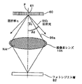
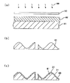
- 229920002120 photoresistant polymer Polymers 0.000 description 33
- 230000008569 process Effects 0.000 description 20
- 239000000758 substrate Substances 0.000 description 15
- 230000000694 effects Effects 0.000 description 10
- 229910052782 aluminium Inorganic materials 0.000 description 7
- XAGFODPZIPBFFR-UHFFFAOYSA-N aluminium Chemical compound [Al] XAGFODPZIPBFFR-UHFFFAOYSA-N 0.000 description 7
- 238000010586 diagram Methods 0.000 description 7
- 210000004027 cell Anatomy 0.000 description 5
- 230000008859 change Effects 0.000 description 5
- 210000002858 crystal cell Anatomy 0.000 description 4
- 238000000206 photolithography Methods 0.000 description 4
- 230000003287 optical effect Effects 0.000 description 3
- 239000000463 material Substances 0.000 description 2
- 238000000059 patterning Methods 0.000 description 2
- 238000003672 processing method Methods 0.000 description 2
- 210000001747 pupil Anatomy 0.000 description 2
- 230000009467 reduction Effects 0.000 description 2
- VYZAMTAEIAYCRO-UHFFFAOYSA-N Chromium Chemical compound [Cr] VYZAMTAEIAYCRO-UHFFFAOYSA-N 0.000 description 1
- VAYOSLLFUXYJDT-RDTXWAMCSA-N Lysergic acid diethylamide Chemical compound C1=CC(C=2[C@H](N(C)C[C@@H](C=2)C(=O)N(CC)CC)C2)=C3C2=CNC3=C1 VAYOSLLFUXYJDT-RDTXWAMCSA-N 0.000 description 1
- 230000008901 benefit Effects 0.000 description 1
- 230000001413 cellular effect Effects 0.000 description 1
- 239000004020 conductor Substances 0.000 description 1
- 238000001312 dry etching Methods 0.000 description 1
- 238000005530 etching Methods 0.000 description 1
- 239000011521 glass Substances 0.000 description 1
- 238000005286 illumination Methods 0.000 description 1
- 239000011810 insulating material Substances 0.000 description 1
- 230000001678 irradiating effect Effects 0.000 description 1
- 229910052751 metal Inorganic materials 0.000 description 1
- 239000002184 metal Substances 0.000 description 1
- 238000004377 microelectronic Methods 0.000 description 1
- 238000007747 plating Methods 0.000 description 1
- 229920001690 polydopamine Polymers 0.000 description 1
- 238000002310 reflectometry Methods 0.000 description 1
- 239000004065 semiconductor Substances 0.000 description 1
- 230000035945 sensitivity Effects 0.000 description 1
- 238000001308 synthesis method Methods 0.000 description 1
- 230000002194 synthesizing effect Effects 0.000 description 1
- 238000001039 wet etching Methods 0.000 description 1
Images


Landscapes
- Preparing Plates And Mask In Photomechanical Process (AREA)
- Exposure And Positioning Against Photoresist Photosensitive Materials (AREA)
- Liquid Crystal (AREA)
- Optical Elements Other Than Lenses (AREA)
Priority Applications (1)
| Application Number | Priority Date | Filing Date | Title |
|---|---|---|---|
| JP2001091340A JP3921953B2 (ja) | 2001-03-27 | 2001-03-27 | マスク、マスクの製造方法、微細構造体の製造方法、及び液晶ディスプレイの製造方法 |
Applications Claiming Priority (1)
| Application Number | Priority Date | Filing Date | Title |
|---|---|---|---|
| JP2001091340A JP3921953B2 (ja) | 2001-03-27 | 2001-03-27 | マスク、マスクの製造方法、微細構造体の製造方法、及び液晶ディスプレイの製造方法 |
Publications (3)
| Publication Number | Publication Date |
|---|---|
| JP2002287325A JP2002287325A (ja) | 2002-10-03 |
| JP2002287325A5 JP2002287325A5 (https=) | 2005-03-03 |
| JP3921953B2 true JP3921953B2 (ja) | 2007-05-30 |
Family
ID=18945970
Family Applications (1)
| Application Number | Title | Priority Date | Filing Date |
|---|---|---|---|
| JP2001091340A Expired - Fee Related JP3921953B2 (ja) | 2001-03-27 | 2001-03-27 | マスク、マスクの製造方法、微細構造体の製造方法、及び液晶ディスプレイの製造方法 |
Country Status (1)
| Country | Link |
|---|---|
| JP (1) | JP3921953B2 (https=) |
Families Citing this family (11)
| Publication number | Priority date | Publication date | Assignee | Title |
|---|---|---|---|---|
| JP4515012B2 (ja) * | 2002-08-07 | 2010-07-28 | 大日本印刷株式会社 | パターンデータの作製方法およびフォトマスク |
| JP5031173B2 (ja) * | 2003-03-26 | 2012-09-19 | 大日本印刷株式会社 | 撮像装置と撮像装置におけるマイクロレンズの形成方法 |
| JP5200439B2 (ja) * | 2006-07-21 | 2013-06-05 | 大日本印刷株式会社 | カラーフィルタの製造方法 |
| JP5228390B2 (ja) * | 2006-07-21 | 2013-07-03 | 大日本印刷株式会社 | 階調マスク |
| JP5673718B2 (ja) * | 2006-07-21 | 2015-02-18 | 大日本印刷株式会社 | 階調マスク |
| JP2009237419A (ja) * | 2008-03-28 | 2009-10-15 | Hoya Corp | 多階調フォトマスク及びその製造方法、並びにパターン転写方法 |
| JP2010020146A (ja) * | 2008-07-11 | 2010-01-28 | Fujifilm Corp | カラーフィルタ及びその製造方法、並びに液晶表示装置 |
| JP5510865B2 (ja) * | 2009-03-25 | 2014-06-04 | 住友化学株式会社 | 防眩処理方法、防眩フィルムの製造方法および金型の製造方法 |
| JP5671788B2 (ja) * | 2009-07-13 | 2015-02-18 | 凸版印刷株式会社 | カラーフィルタ基板用フォトマスク及びカラーフィルタ基板 |
| CN102054279A (zh) * | 2009-11-02 | 2011-05-11 | 住友化学株式会社 | 随机图案的生成方法 |
| JP2011118328A (ja) * | 2009-11-02 | 2011-06-16 | Sumitomo Chemical Co Ltd | ランダムパターンの作成方法 |
-
2001
- 2001-03-27 JP JP2001091340A patent/JP3921953B2/ja not_active Expired - Fee Related
Also Published As
| Publication number | Publication date |
|---|---|
| JP2002287325A (ja) | 2002-10-03 |
Similar Documents
| Publication | Publication Date | Title |
|---|---|---|
| JP2816285B2 (ja) | 透明ディスプレイ装置とその製造方法 | |
| US6638667B2 (en) | Fabricating optical elements using a photoresist formed using of a gray level mask | |
| JP3921953B2 (ja) | マスク、マスクの製造方法、微細構造体の製造方法、及び液晶ディスプレイの製造方法 | |
| CN109387889A (zh) | 抗反射结构、显示装置及抗反射结构制作方法 | |
| CN103185981A (zh) | 彩色滤光阵列基板及其制备方法和显示装置 | |
| US11860400B2 (en) | Backlight component, method for manufacturing backlight component, and display device | |
| JP5391670B2 (ja) | 微細構造体の製造方法 | |
| JPH07205322A (ja) | マイクロコーナーキューブ・マイクロコーナーキューブアレイおよびこれらの製造方法およびマイクロコーナーキューブアレイを用いる表示装置 | |
| JP2024502851A (ja) | 投影スクリーン | |
| JP2002311565A (ja) | 微細構造体の製造方法、2値マスク、および2値マスクの製造方法 | |
| JP4000802B2 (ja) | 半透過反射表示パネル及びこれを用いた電気光学装置 | |
| KR20040062069A (ko) | 반사투과형 액정표시장치용 어레이기판과 그 제조방법 | |
| US20070218372A1 (en) | Method For Production Of Micro-Optics Structures | |
| KR100741772B1 (ko) | 액정표시장치용 반투과 반사 시트 및 그 제조방법 | |
| JP2001356673A (ja) | 計算機ホログラムおよびその製造方法、計算機ホログラムを用いた反射板、並びに計算機ホログラムを用いた反射型液晶表示装置 | |
| KR100978367B1 (ko) | 엠보싱 패턴의 제조 방법 | |
| JP4125198B2 (ja) | 液晶表示素子 | |
| JP3675170B2 (ja) | 光学シートおよびそれを用いた画像表示装置 | |
| JP2007193012A (ja) | 部分透過形液晶表示装置及び携帯電話機器と携帯情報端末機器並びに拡散反射層の開口部形成方法 | |
| JPH11305677A (ja) | 反射型液晶表示装置 | |
| CN100374927C (zh) | 透反射式液晶显示装置及其制造方法 | |
| KR20050043647A (ko) | 방현 필름 및 화상 표시 장치 | |
| JP3711803B2 (ja) | ディスプレイ装置 | |
| JP4214723B2 (ja) | 微細構造体の製造方法 | |
| JPH10253977A (ja) | 反射板および露光装置 |
Legal Events
| Date | Code | Title | Description |
|---|---|---|---|
| A521 | Written amendment |
Free format text: JAPANESE INTERMEDIATE CODE: A523 Effective date: 20040401 |
|
| A621 | Written request for application examination |
Free format text: JAPANESE INTERMEDIATE CODE: A621 Effective date: 20040401 |
|
| A977 | Report on retrieval |
Free format text: JAPANESE INTERMEDIATE CODE: A971007 Effective date: 20050920 |
|
| A131 | Notification of reasons for refusal |
Free format text: JAPANESE INTERMEDIATE CODE: A131 Effective date: 20051004 |
|
| RD03 | Notification of appointment of power of attorney |
Free format text: JAPANESE INTERMEDIATE CODE: A7423 Effective date: 20051108 |
|
| A521 | Written amendment |
Free format text: JAPANESE INTERMEDIATE CODE: A523 Effective date: 20051202 |
|
| A131 | Notification of reasons for refusal |
Free format text: JAPANESE INTERMEDIATE CODE: A131 Effective date: 20060104 |
|
| A521 | Written amendment |
Free format text: JAPANESE INTERMEDIATE CODE: A523 Effective date: 20060306 |
|
| TRDD | Decision of grant or rejection written | ||
| A01 | Written decision to grant a patent or to grant a registration (utility model) |
Free format text: JAPANESE INTERMEDIATE CODE: A01 Effective date: 20070130 |
|
| A61 | First payment of annual fees (during grant procedure) |
Free format text: JAPANESE INTERMEDIATE CODE: A61 Effective date: 20070212 |
|
| R150 | Certificate of patent or registration of utility model |
Free format text: JAPANESE INTERMEDIATE CODE: R150 |
|
| FPAY | Renewal fee payment (event date is renewal date of database) |
Free format text: PAYMENT UNTIL: 20100302 Year of fee payment: 3 |
|
| FPAY | Renewal fee payment (event date is renewal date of database) |
Free format text: PAYMENT UNTIL: 20110302 Year of fee payment: 4 |
|
| FPAY | Renewal fee payment (event date is renewal date of database) |
Free format text: PAYMENT UNTIL: 20120302 Year of fee payment: 5 |
|
| FPAY | Renewal fee payment (event date is renewal date of database) |
Free format text: PAYMENT UNTIL: 20120302 Year of fee payment: 5 |
|
| FPAY | Renewal fee payment (event date is renewal date of database) |
Free format text: PAYMENT UNTIL: 20130302 Year of fee payment: 6 |
|
| FPAY | Renewal fee payment (event date is renewal date of database) |
Free format text: PAYMENT UNTIL: 20140302 Year of fee payment: 7 |
|
| S531 | Written request for registration of change of domicile |
Free format text: JAPANESE INTERMEDIATE CODE: R313531 |
|
| R350 | Written notification of registration of transfer |
Free format text: JAPANESE INTERMEDIATE CODE: R350 |
|
| LAPS | Cancellation because of no payment of annual fees |