JP3907931B2 - Game machine - Google Patents
Game machine Download PDFInfo
- Publication number
- JP3907931B2 JP3907931B2 JP2000275717A JP2000275717A JP3907931B2 JP 3907931 B2 JP3907931 B2 JP 3907931B2 JP 2000275717 A JP2000275717 A JP 2000275717A JP 2000275717 A JP2000275717 A JP 2000275717A JP 3907931 B2 JP3907931 B2 JP 3907931B2
- Authority
- JP
- Japan
- Prior art keywords
- game
- state
- payout control
- power supply
- payout
- Prior art date
- Legal status (The legal status is an assumption and is not a legal conclusion. Google has not performed a legal analysis and makes no representation as to the accuracy of the status listed.)
- Expired - Lifetime
Links
Images


Landscapes
- Display Devices Of Pinball Game Machines (AREA)
- Pinball Game Machines (AREA)
Description
【0001】
【発明の属する技術分野】
本発明は、遊技者の操作に応じて遊技が行われるパチンコ遊技機、コイン遊技機、スロット機等の遊技機に関する。
【0002】
【従来の技術】
遊技機の一例として、遊技球などの遊技媒体を発射装置によって遊技領域に発射し、遊技領域に設けられている入賞口などの入賞領域に遊技媒体が入賞すると、所定個の賞球が遊技者に払い出されるものがある。さらに、表示状態が変化可能な可変表示部が設けられ、可変表示部の表示結果があらかじめ定められた特定の表示態様となった場合に所定の遊技価値を遊技者に与えるように構成されたものがある。
【0003】
遊技価値とは、遊技機の遊技領域に設けられた可変入賞球装置の状態が打球が入賞しやすい遊技者にとって有利な状態になることや、遊技者にとって有利な状態となるための権利を発生させたりすることや、景品遊技媒体払出の条件が成立しやすくなる状態になることである。
【0004】
特別図柄を表示する可変表示部を備えた第1種パチンコ遊技機では、特別図柄を表示する可変表示部の表示結果があらかじめ定められた特定の表示態様の組合せとなることを、通常、「大当り」という。大当りが発生すると、例えば、大入賞口が所定回数開放して打球が入賞しやすい大当り遊技状態に移行する。そして、各開放期間において、所定個(例えば10個)の大入賞口への入賞があると大入賞口は閉成する。そして、大入賞口の開放回数は、所定回数(例えば16ラウンド)に固定されている。なお、各開放について開放時間(例えば29.5秒)が決められ、入賞数が所定個に達しなくても開放時間が経過すると大入賞口は閉成する。また、大入賞口が閉成した時点で所定の条件(例えば、大入賞口内に設けられているVゾーンへの入賞)が成立していない場合には、大当り遊技状態は終了する。
【0005】
また、「大当り」の組合せ以外の表示態様の組合せのうち、複数の可変表示部の表示結果のうちの一部が未だに導出表示されていない段階において、既に確定的な、または一時的な表示結果が導出表示されている可変表示部の表示態様が特定の表示態様の組合せとなる表示条件を満たしている状態を「リーチ」という。そして、可変表示部に可変表示される識別情報の表示結果が「大当り」となる条件を満たさない場合には「はずれ」となり、可変表示状態は終了する。遊技者は、大当りをいかにして発生させるかを楽しみつつ遊技を行う。
【0006】
そして、遊技球が遊技盤に設けられている入賞口に遊技球が入賞すると、あらかじめ決められている個数の賞球払出が行われる。遊技の進行は主基板に搭載された遊技制御手段によって制御されるので、入賞にもとづく賞球個数は、遊技制御手段によって決定され、払出制御基板に送信される。なお、以下、遊技制御手段およびその他の制御手段は、遊技機に設けられている各種電気部品を制御するので、それらを電気部品制御手段と呼ぶことがある。
【0007】
【発明が解決しようとする課題】
以上のように、遊技機には、遊技制御手段を初めとする種々の電気部品制御手段が搭載されている。一般に、各電気部品制御手段はマイクロコンピュータを含んだ構成とされる。そのような電気部品制御手段は、一般に、電源電圧が立ち上がると初期化処理を行い初期状態から制御を開始する。すると、停電等の不測の電源断生じ、その後、電源復旧すると初期状態に戻ってしまうので、遊技者が得た遊技価値等が消滅してしまう等の問題が生ずることがある。そのような問題が生じないようにするには、電源電圧値の低下に伴なって発生される所定の信号に応じて遊技制御を中断し、そのときの制御状態を、遊技機に対する電力供給停止中でも電源バックアップされている記憶手段(バックアップ記憶手段)に保存し、電力供給が完全に停止するのを待つように制御すればよい。そのような遊技機は、記憶手段に遊技状態が保存されている状態で電力供給が再開されたら、保存されている制御状態にもとづいて遊技を再開するので、遊技者に不利益が与えられることが防止される。
【0008】
しかし、電源の瞬断等によって極めて短い期間電源電圧が低下したような場合には、電源電圧は直ちに復旧する。そのような場合、マイクロコンピュータの制御が、電力供給が完全に停止するのを待つ状態から抜けきらないことも考えられる。すなわち、遊技機への電力供給は平常時の状態になっているにもかかわらず、遊技機制御が平常時の状態に戻らないことも考えられる。
【0009】
また、電力供給が完全に停止するのを待つ状態であるときには、電源供給が不安定な状態となっていることから、バックアップ記憶の記憶内容が破壊されてしまうおそれがある。
【0010】
そこで、本発明は、不測の電源断時等にそのときの制御状態を保存するように構成されている遊技機において、ごく短時間で復旧する電源の瞬断等が生じても制御に支障を来すことのないようにすることができるとともに、電源供給が不安定な状況下においてもバックアップ記憶の内容の安全を保証することができる遊技機を提供することを目的とする。
【0011】
【課題を解決するための手段】
本発明による遊技機は、遊技媒体を用いて遊技者が所定の遊技を行うことが可能な遊技機であって、遊技媒体を検出するための遊技媒体検出手段と、制御を行う際に発生する変動データを記憶する遊技制御用変動データ記憶手段を有し、遊技の進行を制御する遊技制御用マイクロコンピュータと、制御を行う際に発生する変動データを記憶する払出制御用変動データ記憶手段を有し、遊技媒体の払出を行う払出手段を動作させて遊技媒体の払出の制御を行う払出制御用マイクロコンピュータと、遊技機への電力供給が停止していても遊技制御用変動データ記憶手段および払出制御用変動データ記憶手段の記憶内容を所定期間保持させることが可能な記憶内容保持手段と、遊技媒体検出手段に供給される電圧よりも高い電圧を監視して電源断の発生を検出したときに検出信号を出力する電源監視手段とを備え、遊技制御用マイクロコンピュータは、検出信号の入力に応じて、バックアップフラグを遊技制御用変動データ記憶手段に設定する処理、遊技制御用変動データ記憶手段の記憶内容が正常か否かの判定に用いるチェックデータの作成処理、および遊技制御用変動データ記憶手段へのアクセスを禁止する処理を含む遊技制御用電力供給停止時処理を行った後に待機状態に移行し、払出制御用マイクロコンピュータは、検出信号の入力に応じて、払出手段の動作を停止させる処理、バックアップフラグを払出制御用変動データ記憶手段に設定する処理、払出制御用変動データ記憶手段の記憶内容が正常か否かの判定に用いるチェックデータの作成処理、および払出制御用変動データ記憶手段へのアクセスを禁止する処理を含む払出制御用電力供給停止時処理を行った後に待機状態に移行し、払出制御用電力供給停止時処理において、払出手段の動作を停止させる処理をバックアップフラグを設定する処理、チェックデータを作成する処理および払出制御用変動データ記憶手段へのアクセスを禁止する処理より先に実行し、電源監視手段が検出信号を出力した後の所定期間経過後に電力供給が停止していないときに、待機状態から復帰させるための復帰信号を出力する復帰信号出力手段を備え、遊技制御用マイクロコンピュータは、電力供給が開始されたときまたは待機状態中に復帰信号が入力されたときに、遊技制御用変動データ記憶手段にバックアップフラグが設定されていることおよびチェックデータにもとづいて遊技制御用変動データ記憶手段の記憶内容が正常であることを確認したことを条件に、遊技制御用変動データ記憶手段の記憶内容にもとづいて制御状態を遊技制御用電力供給停止時処理を開始したときの状態に復帰させる遊技制御用状態復帰制御を実行し、遊技制御用変動データ記憶手段にバックアップフラグが設定されていなければ、遊技制御用変動データ記憶手段の記憶内容が正常であるか否かにかかわらず遊技制御用変動データ記憶手段の記憶内容を初期化する処理を実行し、払出制御用マイクロコンピュータは、電力供給が開始されたときまたは待機状態中に復帰信号が入力されたときに、払出制御用変動データ記憶手段にバックアップフラグが設定されていることおよびチェックデータにもとづいて払出制御用変動データ記憶手段の記憶内容が正常であることを確認したことを条件に、払出制御用変動データ記憶手段の記憶内容にもとづいて制御状態を払出制御用電力供給停止時処理を開始したときの状態に復帰させる払出制御用状態復帰制御を実行し、払出制御用変動データ記憶手段にバックアップフラグが設定されていなければ、払出制御用変動データ記憶手段の記憶内容が正常であるか否かにかかわらず払出制御用変動データ記憶手段の記憶内容を初期化する処理を実行することを特徴とする。
【0013】
復帰信号出力手段は、遊技制御用マイクロコンピュータに復帰信号を出力する第1の復帰信号出力手段と、払出制御用マイクロコンピュータに復帰信号を出力する第2の復帰信号出力手段とを含み、第2の復帰信号出力手段が払出制御用マイクロコンピュータに復帰信号を出力した後に、第1の復帰信号出力手段が遊技制御用マイクロコンピュータに復帰信号を出力するように構成されていてもよい。
【0014】
遊技媒体検出手段は、払出手段から払い出された遊技媒体を検出し、払出制御用マイクロコンピュータは、電源監視手段が検出信号を出力したときに、遊技媒体検出手段からの検出信号の入力処理を所定の検出期間実行した後、払出制御用電力供給停止時処理を行うように構成されていてもよい。
【0015】
払出制御用マイクロコンピュータは、出力ポートを介して払出手段に駆動信号を出力し、電源監視手段が検出信号を出力したときに、払出手段の駆動を停止した後、遊技媒体検出手段からの検出信号の入力処理を実行するように構成されていてもよい。
【0016】
電源監視手段が検出信号を出力した後の、払出制御用マイクロコンピュータによる遊技媒体検出手段からの検出信号の入力処理の実行中に、払出制御用マイクロコンピュータおよび遊技媒体検出手段を駆動可能な電源を供給可能な補助駆動電源供給手段を備えていることが好ましい。
【0017】
遊技媒体検出手段として、入賞に応じて払出手段から払い出された遊技媒体を検出する賞遊技媒体検出手段と、貸出要求に応じて払出手段から払い出された遊技媒体を検出する貸出遊技媒体検出手段とを別個に設けてもよい。
【0018】
払出制御用マイクロコンピュータは、電力供給が開始されたときに、定期的にタイマ割込が発生するように設定し、定期的に発生するタイマ割込が生じたことにもとづいて遊技媒体の払出の制御を行うための割込処理を実行し、割込禁止条件の成立にもとづいて割込処理の実行を禁止する割込禁止状態に設定し、払出制御用電力供給停止時処理にて、割込禁止状態または実行を許可する割込許可状態のうちいずれの状態であるかを示す割込状態データを変動データ記憶手段に保存させる処理を実行し、電力供給が開始されたときに、割込状態データにもとづいて割込禁止状態または割込許可状態に復旧させる状態復旧処理を行うように構成されていてもよい。
【0019】
遊技制御用マイクロコンピュータは、入賞に応じた遊技媒体の払出数を指定する払出制御コマンドを払出制御用マイクロコンピュータに送信し、払出制御用マイクロコンピュータは、払出制御コマンドの受信に応じて、払出手段を制御して払出制御コマンドで指定された払出数の遊技媒体の払い出しを行い、払出制御コマンドを受信しているときは、割込禁止状態に制御するように構成されていてもよい。
【0020】
遊技制御用マイクロコンピュータは、電力供給が開始されたときに、定期的にタイマ割込が発生するように設定し、定期的に発生するタイマ割込が生じたことにもとづいて遊技の進行を制御するための割込処理を実行し、割込禁止条件の成立にもとづいて割込処理の実行を禁止する割込禁止状態に設定し、遊技制御用電力供給停止時処理にて、割込禁止状態または実行を許可する割込許可状態のうちいずれの状態であるかを示す割込状態データを遊技制御用変動データ記憶手段に保存させる処理を実行し、電力供給が開始されたときに、割込状態データにもとづいて割込禁止状態または割込許可状態に復旧させる状態復旧処理を行うように構成されていてもよい。
【0021】
【発明の実施の形態】
以下、本発明の一実施形態を図面を参照して説明する。
まず、遊技機の一例であるパチンコ遊技機の全体の構成について説明する。図1はパチンコ遊技機1を正面からみた正面図である。なお、ここでは、遊技機の一例としてパチンコ遊技機を示すが、本発明はパチンコ遊技機に限られず、例えばコイン遊技機やスロット機等であってもよい。
【0022】
図1に示すように、パチンコ遊技機1は、額縁状に形成されたガラス扉枠2を有する。ガラス扉枠2の下部表面には打球供給皿3がある。打球供給皿3の下部には、打球供給皿3からあふれた遊技球を貯留する余剰玉受皿4と打球を発射する打球操作ハンドル(操作ノブ)5が設けられている。ガラス扉枠2の後方には、遊技盤6が着脱可能に取り付けられている。また、遊技盤6の前面には遊技領域7が設けられている。
【0023】
遊技領域7の中央付近には、複数種類の図柄を可変表示するための可変表示部(特別図柄表示装置)9と7セグメントLEDによる普通図柄表示器(普通図柄表示装置)10とを含む可変表示装置8が設けられている。可変表示部9には、例えば「左」、「中」、「右」の3つの図柄表示エリアがある。可変表示装置8の側部には、打球を導く通過ゲート11が設けられている。通過ゲート11を通過した打球は、玉出口13を経て始動入賞口14の方に導かれる。通過ゲート11と玉出口13との間の通路には、通過ゲート11を通過した打球を検出するゲートスイッチ12がある。また、始動入賞口14に入った入賞球は、遊技盤6の背面に導かれ、始動口スイッチ17によって検出される。また、始動入賞口14の下部には開閉動作を行う可変入賞球装置15が設けられている。可変入賞球装置15は、ソレノイド16によって開状態とされる。
【0024】
可変入賞球装置15の下部には、特定遊技状態(大当り状態)においてソレノイド21によって開状態とされる開閉板20が設けられている。この実施の形態では、開閉板20が大入賞口を開閉する手段となる。開閉板20から遊技盤6の背面に導かれた入賞球のうち一方(Vゾーン)に入った入賞球はV入賞スイッチ22で検出される。また、開閉板20からの入賞球はカウントスイッチ23で検出される。可変表示装置8の下部には、始動入賞口14に入った入賞球数を表示する4個の表示部を有する始動入賞記憶表示器18が設けられている。この例では、4個を上限として、始動入賞がある毎に、始動入賞記憶表示器18は点灯している表示部を1つずつ増やす。そして、可変表示部9の可変表示が開始される毎に、点灯している表示部を1つ減らす。
【0025】
遊技盤6には、複数の入賞口19,24が設けられ、遊技球のそれぞれの入賞口19,24への入賞は、対応して設けられている入賞口スイッチ19a,19b,24a,24bによって検出される。遊技領域7の左右周辺には、遊技中に点滅表示される装飾ランプ25が設けられ、下部には、入賞しなかった打球を吸収するアウト口26がある。また、遊技領域7の外側の左右上部には、効果音を発する2つのスピーカ27が設けられている。遊技領域7の外周には、遊技効果LED28aおよび遊技効果ランプ28b,28cが設けられている。
【0026】
そして、この例では、一方のスピーカ27の近傍に、賞球残数があるときに点灯する賞球ランプ51が設けられ、他方のスピーカ27の近傍に、補給球が切れたときに点灯する球切れランプ52が設けられている。さらに、図1には、パチンコ遊技機1に隣接して設置され、プリペイドカードが挿入されることによって球貸しを可能にするカードユニット50も示されている。
【0027】
カードユニット50には、使用可能状態であるか否かを示す使用可表示ランプ151、カード内に記録された残額情報に端数(100円未満の数)が存在する場合にその端数を打球供給皿3の近傍に設けられる度数表示LEDに表示させるための端数表示スイッチ152、カードユニット50がいずれの側のパチンコ遊技機1に対応しているのかを示す連結台方向表示器153、カードユニット50内にカードが投入されていることを示すカード投入表示ランプ154、記録媒体としてのカードが挿入されるカード挿入口155、およびカード挿入口155の裏面に設けられているカードリーダライタの機構を点検する場合にカードユニット50を解放するためのカードユニット錠156が設けられている。
【0028】
打球発射装置から発射された打球は、打球レールを通って遊技領域7に入り、その後、遊技領域7を下りてくる。打球が通過ゲート11を通ってゲートスイッチ12で検出されると、普通図柄表示器10の表示数字が連続的に変化する状態になる。また、打球が始動入賞口14に入り始動口スイッチ17で検出されると、図柄の変動を開始できる状態であれば、可変表示部9内の図柄が回転を始める。図柄の変動を開始できる状態でなければ、始動入賞記憶を1増やす。
【0029】
可変表示部9内の画像の回転は、一定時間が経過したときに停止する。停止時の画像の組み合わせが大当り図柄の組み合わせであると、大当り遊技状態に移行する。すなわち、開閉板20が、一定時間経過するまで、または、所定個数(例えば10個)の打球が入賞するまで開放する。そして、開閉板20の開放中に打球が特定入賞領域に入賞しV入賞スイッチ22で検出されると、継続権が発生し開閉板20の開放が再度行われる。継続権の発生は、所定回数(例えば15ラウンド)許容される。
【0030】
停止時の可変表示部9内の画像の組み合わせが確率変動を伴う大当り図柄の組み合わせである場合には、次に大当りとなる確率が高くなる。すなわち、高確率状態という遊技者にとってさらに有利な状態となる。また、普通図柄表示器10における停止図柄が所定の図柄(当り図柄=小当り図柄)である場合に、可変入賞球装置15が所定時間だけ開状態になる。さらに、高確率状態では、普通図柄表示器10における停止図柄が当り図柄になる確率が高められるとともに、可変入賞球装置15の開放時間と開放回数が高められる。
【0031】
次に、パチンコ遊技機1の裏面に配置されている各基板について説明する。
図2に示すように、パチンコ遊技機1の裏面では、枠体2A内の機構板の上部に玉貯留タンク38が設けられ、パチンコ遊技機1が遊技機設置島に設置された状態でその上方から遊技球が球貯留タンク38に供給される。球貯留タンク38内の遊技球は、誘導樋39を通って賞球ケース40Aで覆われる球払出装置に至る。
【0032】
遊技機裏面側では、可変表示部9を制御する可変表示制御ユニット29、遊技制御用マイクロコンピュータ等が搭載された遊技制御基板(主基板)31が設置されている。また、球払出制御を行う払出制御用マイクロコンピュータ等が搭載された払出制御基板37、およびモータの回転力を利用して打球を遊技領域7に発射する打球発射装置が設置されている。さらに、装飾ランプ25、遊技効果LED28a、遊技効果ランプ28b,28c、賞球ランプ51および球切れランプ52に信号を送るためのランプ制御基板35、スピーカ27からの音声発生を制御するための音声制御基板70および打球発射装置を制御するための発射制御基板91も設けられている。
【0033】
さらに、DC30V、DC21V、DC12VおよびDC5Vを作成する電源回路が搭載された電源基板910が設けられ、上方には、各種情報を遊技機外部に出力するための各端子を備えたターミナル基板160が設置されている。ターミナル基板160には、少なくとも、球切れ検出スイッチの出力を導入して外部出力するための球切れ用端子、賞球個数信号を外部出力するための賞球用端子および球貸し個数信号を外部出力するための球貸し用端子が設けられている。また、中央付近には、主基板31からの各種情報を遊技機外部に出力するための各端子を備えた情報端子盤34が設置されている。なお、図2には、ランプ制御基板35および音声制御基板70からの信号を、枠側に設けられている遊技効果LED28a、遊技効果ランプ28b,28c、賞球ランプ51および球切れランプ52に供給するための電飾中継基板A77が示されているが、信号中継の必要に応じて他の中継基板も設けられる。
【0034】
図3はパチンコ遊技機1の機構板を背面からみた背面図である。球貯留タンク38に貯留された玉は誘導樋39を通り、図3に示されるように、球切れ検出器(球切れスイッチ)187a,187bを通過して球供給樋186a,186bを経て球払出装置97に至る。球切れスイッチ187a,187bは遊技球通路内の遊技球の有無を検出するスイッチであるが、球タンク38内の補給球の不足を検出する球切れ検出スイッチ167も設けられている。以下、球切れスイッチ187a,187bを、球切れスイッチ187と表現することがある。
【0035】
球払出装置97から払い出された遊技球は、連絡口45を通ってパチンコ遊技機1の前面に設けられている打球供給皿3に供給される。連絡口45の側方には、パチンコ遊技機1の前面に設けられている余剰玉受皿4に連通する余剰玉通路46が形成されている。
【0036】
入賞にもとづく景品球が多数払い出されて打球供給皿3が満杯になり、ついには遊技球が連絡口45に到達した後さらに遊技球が払い出されると遊技球は、余剰玉通路46を経て余剰玉受皿4に導かれる。さらに遊技球が払い出されると、感知レバー47が満タンスイッチ48を押圧して満タンスイッチ48がオンする。その状態では、球払出装置97内のステッピングモータの回転が停止して球払出装置97の動作が停止するとともに打球発射装置の駆動も停止する。
【0037】
次に、機構板36に設置されている中間ベースユニットの構成について説明する。中間ベースユニットには、球供給樋186a,186bや球払出装置97が設置される。図4に示すように、中間ベースユニットの上下には連結凹突部182が形成されている。連結凹突部182は、中間ベースユニットと機構板36の上部ベースユニットおよび下部ベースユニットを連結固定するものである。
【0038】
中間ベースユニットの上部には通路体184が固定されている。そして、通路体184の下部に球払出装置97が固定されている。通路体184は、カーブ樋174(図3参照)によって流下方向を左右方向に変換された2列の遊技球を流下させる払出球通路186a,186bを有する。払出球通路186a,186bの上流側には、球切れスイッチ187a,187bが設置されている。球切れスイッチ187a,187bは、払出球通路186a,186b内の遊技球の有無を検出するものであって、球切れスイッチ187a,187bが遊技球を検出しなくなると球払出装置97における払出モータ(図4において図示せず)の回転を停止して球払出が不動化される。
【0039】
なお、球切れスイッチ187a,187bは、払出球通路186a,186bに27〜28個程度の遊技球が存在することを検出できるような位置に係止片188によって係止されている。すなわち、球切れスイッチ187a,187bは、賞球の一単位の最大払出量(この実施の形態では15個)および球貸しの一単位の最大払出量(この実施の形態では100円:25個)以上が確保されていることが確認できるような位置に設置されている。
【0040】
通路体184の中央部は、内部を流下する遊技球の球圧を弱めるように、左右に湾曲する形状に形成されている。そして、払出球通路186a,186bの間に止め穴189が形成されている。止め穴189の裏面は中間ベースユニットに設けられている取付ボスがはめ込まれる。その状態で止めねじがねじ止めされて、通路体184は中間ベースユニットに固定される。なお、ねじ止めされる前に、中間ベースユニットに設けられている係止突片185によって通路体184の位置合わせを行えるようになっている。
【0041】
通路体184の下方には、球払出装置97に遊技球を供給するとともに故障時等には球払出装置97への遊技球の供給を停止する球止め装置190が設けられている。球止め装置190の下方に設置される球払出装置97は、直方体状のケース198の内部に収納されている。ケース198の左右4箇所には突部が設けられている。各突部が中間ベースユニットに設けられている位置決め突片に係った状態で、中間ベースユニットの下部に設けられている弾性係合片にケース198の下端がはめ込まれる。
【0042】
図5は球払出装置97の分解斜視図である。球払出装置97の構成および作用について図5を参照して説明する。この実施形態における球払出装置97は、ステッピングモータ(払出モータ)289がスクリュー288を回転させることによりパチンコ玉を1個ずつ払い出す。なお、球払出装置97は、入賞にもとづく景品球だけでなく、貸し出すべき遊技球も払い出す。
【0043】
図5に示すように、球払出装置97は、2つのケース198a,198bを有する。それぞれのケース198a,198bの左右2箇所に、球払出装置97の設置位置上部に設けられた位置決め突片に当接される係合突部280が設けられている。また、それぞれのケース198a,198bには、球供給路281a,281bが形成されている。球供給路281a,281bは湾曲面282a,282bを有し、湾曲面282a,282bの終端の下方には、球送り水平路284a,284bが形成されている。さらに、球送り水平路284a,284bの終端に球排出路283a,283bが形成されている。
【0044】
球供給路281a,281b、球送り水平路284a,284b、球排出路283a,283bは、ケース198a,198bをそれぞれ前後に区画する区画壁295a,295bの前方に形成されている。また、区画壁295a,295bの前方において、玉圧緩衝部材285がケース198a,198b間に挟み込まれる。玉圧緩衝部材285は、球払出装置97に供給される玉を左右側方に振り分けて球供給路281a,281bに誘導する。
【0045】
また、玉圧緩衝部材285の下部には、発光素子(LED)286と受光素子(図示せず)とによる払出モータ位置センサが設けられている。発光素子286と受光素子とは、所定の間隔をあけて設けられている。そして、この間隔内に、スクリュー288の先端が挿入されるようになっている。なお、玉圧緩衝部材285は、ケース198a,198bが張り合わされたときに、完全にその内部に収納固定される。
【0046】
球送り水平路284a,284bには、払出モータ289によって回転させられるスクリュー288が配置されている。払出モータ289はモータ固定板290に固定され、モータ固定板290は、区画壁295a,295bの後方に形成される固定溝291a,291bにはめ込まれる。その状態で払出モータ289のモータ軸が区画壁295a,295bの前方に突出するので、その突出の前方にスクリュー288が固定される。スクリュー288の外周には、払出モータ289の回転によって球送り水平路284a,284bに載置された遊技球を前方に移動させるための螺旋突起288aが設けられている。
【0047】
そして、スクリュー288の先端には、発光素子286を収納するように凹部が形成され、その凹部の外周には、2つの切欠部292が互いに180度離れて形成されている。従って、スクリュー288が1回転する間に、発光素子286からの光は、切欠部292を介して受光素子で2回検出される。
【0048】
つまり、発光素子286と受光素子とによる払出モータ位置センサは、スクリュー288を定位置で停止するためのものであり、かつ、払出動作が行われた旨を検出するものである。なお、発光素子286、受光素子および払出モータ289からの配線は、まとめられてケース198a,198bの後部下方に形成された引出穴から外部に引き出されコネクタに結線される。
【0049】
遊技球が球送り水平路284a,284bに載置された状態において、払出モータ289が回転すると、スクリュー288の螺旋突起288aによって、遊技球は、球送り水平路284a,284b上を前方に向かって移動する。そして、遂には、球送り水平路284a,284bの終端から球排出路283a,283bに落下する。このとき、左右の球送り水平路284a,284bからの落下は交互に行われる。すなわち、スクリュー288が半回転する毎に一方から1個の遊技球が落下する。従って、1個の遊技球が落下する毎に、発光素子286からの光が受光素子によって検出される。
【0050】
図4に示すように、球払出装置97の下方には、球振分部材311が設けられている。球振分部材311は、振分ソレノイド310によって駆動される。例えば、ソレノイド310のオン時には、球振分部材311は右側に倒れ、オフ時には左側に倒れる。振分ソレノイド310の下方には、近接スイッチによる賞球カウントスイッチ301Aおよび球貸しカウントスイッチ301Bが設けられている。入賞にもとづく賞球時には、球振分部材311は右側に倒れ、球排出路283a,283bからの玉はともに賞球カウントスイッチ301Aを通過する。また、球貸し時には、球振分部材311は左側に倒れ、球排出路283a,283bからの玉はともに球貸しカウントスイッチ301Bを通過する。従って、球払出装置97は、賞球時と球貸し時とで払出流下路を切り替えて、所定数の遊技媒体の払出を行うことができる。
【0051】
このように、球振分部材311を設けることによって、2条の玉流路を落下してきた玉は、賞球カウントスイッチ301Aと球貸しカウントスイッチ301Bとのうちのいずれか一方しか通過しない。従って、賞球であるのか球貸しであるのかの判断をすることなく、賞球カウントスイッチ301Aと球貸しカウントスイッチ301Bの検出出力から、直ちに賞球数または球貸し数を把握することができる。
【0052】
なお、この実施の形態では、電気的駆動源の駆動によって遊技球を払い出す球払出装置として、ステッピングモータの回転によって遊技球が払い出される球払出装置97を用いることにするが、その他の駆動源によって遊技球を送り出す構造の球払出装置を用いてもよいし、電気的駆動源の駆動によってストッパを外し遊技球の自重によって払い出しがなされる構造の球払出装置を用いてもよい。また、この実施の形態では、球払出装置97は賞球にもとづく景品球と貸出要求にもとづく貸し球の双方を払い出すが、それぞれについて払出装置が設けられていてもよい。
【0053】
図6は、主基板31における回路構成の一例を示すブロック図である。なお、図6には、払出制御基板37、ランプ制御基板35、音声制御基板70、発射制御基板91および図柄制御基板80も示されている。主基板31には、プログラムに従ってパチンコ遊技機1を制御する基本回路53と、ゲートスイッチ12、始動口スイッチ17、V入賞スイッチ22、カウントスイッチ23、入賞口スイッチ19a,19b,24a,24b、満タンスイッチ48、球切れスイッチ187および賞球カウントスイッチ301Aからの信号を基本回路53に与えるスイッチ回路58と、可変入賞球装置15を開閉するソレノイド16、開閉板20を開閉するソレノイド21および大入賞口内の経路を切り換えるためのソレノイド21Aを基本回路53からの指令に従って駆動するソレノイド回路59とが搭載されている。
【0054】
なお、図6には示されていないが、カウントスイッチ短絡信号もスイッチ回路58を介して基本回路53に伝達される。
【0055】
また、基本回路53から与えられるデータに従って、大当りの発生を示す大当り情報、可変表示部9の画像表示開始に利用された始動入賞球の個数を示す有効始動情報、確率変動が生じたことを示す確変情報等の情報出力信号をホールコンピュータ等の外部機器に対して出力する情報出力回路64が搭載されている。
【0056】
基本回路53は、ゲーム制御用のプログラム等を記憶するROM54、ワークメモリとして使用される記憶手段の一例であるRAM55、プログラムに従って制御動作を行うCPU56およびI/Oポート部57を含む。この実施の形態では、ROM54,RAM55はCPU56に内蔵されている。すなわち、CPU56は、1チップマイクロコンピュータである。なお、1チップマイクロコンピュータは、少なくともRAM55が内蔵されていればよく、ROM54およびI/Oポート部57は外付けであっても内蔵されていてもよい。
【0057】
遊技球を打撃して発射する打球発射装置は発射制御基板91上の回路によって制御される駆動モータ94で駆動される。そして、駆動モータ94の駆動力は、操作ノブ5の操作量に従って調整される。すなわち、発射制御基板91上の回路によって、操作ノブ5の操作量に応じた速度で打球が発射されるように制御される。
【0058】
この実施の形態では、電源基板910から主基板31に対して、ローレベルがリセット状態を示すリセット信号、ローアクティブの復帰信号およびローアクティブの電源断信号も入力される。リセット信号と復帰信号とはAND回路161に入力され、AND回路161の出力がCPU56のリセット端子に入力される。また、電源断信号は、CPU56のマスク不能割込(NMI)端子に入力される。さらに、図6には明示されていないが、RAM(CPU内蔵RAMであってもよい)55の少なくとも一部は、電源基板910において作成されるバックアップ電源よって、バックアップされている。すなわち、遊技機に対する電力供給が停止しても、所定期間は、RAM55の少なくとも一部の内容は保存される。
【0059】
なお、この実施の形態では、ランプ制御基板35に搭載されているランプ制御手段が、遊技盤に設けられている始動記憶表示器18、ゲート通過記憶表示器41および装飾ランプ25の表示制御を行うとともに、枠側に設けられている遊技効果ランプ・LED28a,28b,28c、賞球ランプ51および球切れランプ52の表示制御を行う。また、特別図柄を可変表示する可変表示部9および普通図柄を可変表示する普通図柄表示器10の表示制御は、図柄制御基板80に搭載されている表示制御手段によって行われる。
【0060】
図7は、払出制御基板37および球払出装置97の構成要素などの払出に関連する構成要素を示すブロック図である。図7に示すように、満タンスイッチ48からの検出信号は、中継基板71を介して主基板31のI/Oポート部57に入力される。満タンスイッチ48は、余剰球受皿4の満タンを検出するスイッチである。また、球切れスイッチ187(187a,187b)からの検出信号も、中継基板72および中継基板71を介して主基板31のI/Oポート部57に入力される。
【0061】
主基板31のCPU56は、球切れスイッチ187からの検出信号が球切れ状態を示しているか、または、満タンスイッチ48からの検出信号が満タン状態を示していると、払出禁止を指示する払出制御コマンドを送出する。払出禁止を指示する払出制御コマンドを受信すると、払出制御基板37の払出制御用CPU371は球払出処理を停止する。
【0062】
さらに、賞球カウントスイッチ301Aからの検出信号は、中継基板72および中継基板71を介して主基板31のI/Oポート部57に入力されるとともに、中継基板72を介して払出制御基板37の入力ポート372bに入力される。賞球カウントスイッチ301Aは、球払出装置97の払出機構部分に設けられ、実際に払い出された賞球払出球を検出する。
【0063】
入賞があると、払出制御基板37には、主基板31の出力ポート(ポート0,1)570,571から賞球個数を示す払出制御コマンドが入力される。出力ポート(出力ポート1)571は8ビットのデータを出力し、出力ポート570は1ビットのストローブ信号(INT信号)を出力する。賞球個数を示す払出制御コマンドは、入力バッファ回路373Aを介してI/Oポート372aに入力される。INT信号は、入力バッファ回路373Bを介して払出制御用CPU371の割込端子に入力されている。払出制御用CPU371は、I/Oポート372aを介して払出制御コマンドを入力し、払出制御コマンドに応じて球払出装置97を駆動して賞球払出を行う。なお、この実施の形態では、払出制御用CPU371は、1チップマイクロコンピュータであり、少なくともRAMが内蔵されている。
【0064】
また、主基板31において、出力ポート570,571の外側にバッファ回路620,68Aが設けられている。バッファ回路620,68Aとして、例えば、汎用のCMOS−ICである74HC250,74HC14が用いられる。このような構成によれば、外部から主基板31の内部に入力される信号が阻止されるので、払出制御基板37から主基板31に信号が与えられる可能性がある信号ラインをさらに確実になくすことができる。なお、バッファ回路620,68Aの出力側にノイズフィルタを設けてもよい。
【0065】
払出制御用CPU371は、出力ポート372cを介して、貸し球数を示す球貸し個数信号をターミナル基板160に出力する。さらに、出力ポート372dを介して、エラー表示用LED374にエラー信号を出力する。
【0066】
さらに、払出制御基板37の入力ポート372bには、中継基板72を介して球貸しカウントスイッチ301Bからの検出信号が入力される。球貸しカウントスイッチ301Bは、球払出装置97の払出機構部分に設けられ、実際に払い出された貸し球を検出する。払出制御基板37からの払出モータ289への駆動信号はあ、出力ポート372cおよび中継基板72を介して球払出装置97の払出機構部分における払出モータ289に伝えられ、振分ソレノイド310への駆動信号は、出力ポート372eおよび中継基板72を介して球払出装置97の払出機構部分における振分ソレノイド310に伝えられる。
【0067】
カードユニット50には、カードユニット制御用マイクロコンピュータが搭載されている。また、カードユニット50には、端数表示スイッチ152、連結台方向表示器153、カード投入表示ランプ154およびカード挿入口155が設けられている(図1参照)。残高表示基板74には、打球供給皿3の近傍に設けられている度数表示LED、球貸しスイッチおよび返却スイッチが接続される。
【0068】
残高表示基板74からカードユニット50には、遊技者の操作に応じて、球貸しスイッチ信号および返却スイッチ信号が払出制御基板37を介して与えられる。また、カードユニット50から残高表示基板74には、プリペイドカードの残高を示すカード残高表示信号および球貸し可表示信号が払出制御基板37を介して与えられる。カードユニット50と払出制御基板37の間では、接続信号(VL信号)、ユニット操作信号(BRDY信号)、球貸し要求信号(BRQ信号)、球貸し完了信号(EXS信号)およびパチンコ機動作信号(PRDY信号)が入力ポート372bおよび出力ポート372eを介してやりとりされる。
【0069】
パチンコ遊技機1の電源が投入されると、払出制御基板37の払出制御用CPU371は、カードユニット50にPRDY信号を出力する。また、カードユニット制御用マイクロコンピュータは、VL信号を出力する。払出制御用CPU371は、VL信号の入力状態により接続状態/未接続状態を判定する。カードユニット50においてカードが受け付けられ、球貸しスイッチが操作され球貸しスイッチ信号が入力されると、カードユニット制御用マイクロコンピュータは、払出制御基板37にBRDY信号を出力する。この時点から所定の遅延時間が経過すると、カードユニット制御用マイクロコンピュータは、払出制御基板37にBRQ信号を出力する。
【0070】
そして、払出制御基板37の払出制御用CPU371は、カードユニット50に対するEXS信号を立ち上げ、カードユニット50からのBRQ信号の立ち下がりを検出すると、払出モータ289を駆動し、所定個の貸し球を遊技者に払い出す。このとき、振分ソレノイド310は駆動状態とされている。すなわち、球振分部材311を球貸し側に向ける。そして、払出が完了したら、払出制御用CPU371は、カードユニット50に対するEXS信号を立ち下げる。その後、カードユニット50からのBRDY信号がオン状態でなければ、賞球払出制御を実行する。
【0071】
以上のように、カードユニット50からの信号は全て払出制御基板37に入力される構成になっている。従って、球貸し制御に関して、カードユニット50から主基板31に信号が入力されることはなく、主基板31の基本回路53にカードユニット50の側から不正に信号が入力される余地はない。また、カードユニット50で用いられる電源電圧AC24Vは払出制御基板37から供給される。
【0072】
この実施の形態では、電源基板910から払出制御基板37に対して、リセット信号、復帰信号および電源断信号も入力される。リセット信号と復帰信号とはAND回路385に入力され、AND回路385の出力が払出制御用CPU371のリセット端子に入力される。また、電源断信号は、払出制御用CPU371のマスク不能割込(NMI)端子に入力される。さらに、払出制御基板37に存在するRAM(CPU内蔵RAMであってもよい。)の少なくとも一部は、電源基板910において作成されるバックアップ電源によって、バックアップされている。すなわち、遊技機に対する電力供給が停止しても、所定期間は、RAMの少なくとも一部の内容は保存される。
【0073】
なお、この実施の形態では、カードユニット50が遊技機とは別体として遊技機に隣接して設置されている場合を例にするが、カードユニット50は遊技機と一体化されていてもよい。また、コイン投入に応じてその金額に応じた遊技球が貸し出されるような場合でも本発明を適用できる。
【0074】
図8は、図柄制御基板80内の回路構成を、可変表示部9の一実現例であるLCD(液晶表示装置)82、可変表示器10、主基板31の出力ポート(ポート0,2)570,572および出力バッファ回路620,62Aとともに示すブロック図である。出力ポート(出力ポート2)572からは8ビットのデータが出力され、出力ポート570からは1ビットのストローブ信号(INT信号)が出力される。
【0075】
図8に示すように、表示制御用CPU101には、電源基板910からリセット信号が供給されている。リセット信号がローレベルであると表示制御用CPU101はリセット状態となり、リセット信号がハイレベルになると表示制御用CPU101は動作可能状態になる。
【0076】
表示制御用CPU101は、制御データROM102に格納されたプログラムに従って動作し、主基板31からノイズフィルタ107および入力バッファ回路105Bを介してINT信号が入力されると、入力バッファ回路105Aを介して表示制御コマンドを受信する。入力バッファ回路105A,105Bとして、例えば汎用ICである74HC540,74HC14を使用することができる。なお、表示制御用CPU101がI/Oポートを内蔵していない場合には、入力バッファ回路105A,105Bと表示制御用CPU101との間に、I/Oポートが設けられる。
【0077】
そして、表示制御用CPU101は、受信した表示制御コマンドに従って、LCD82に表示される画面の表示制御を行う。具体的には、表示制御コマンドに応じた指令をVDP103に与える。VDP103は、キャラクタROM86から必要なデータを読み出す。VDP103は、入力したデータに従ってLCD82に表示するための画像データを生成し、R,G,B信号および同期信号をLCD82に出力する。
【0078】
なお、図8には、VDP103をリセットするためのリセット回路83、VDP103に動作クロックを与えるための発振回路85、および使用頻度の高い画像データを格納するキャラクタROM86も示されている。キャラクタROM86に格納される使用頻度の高い画像データとは、例えば、LCD82に表示される人物、動物、または、文字、図形もしくは記号等からなる画像などである。
【0079】
入力バッファ回路105A,105Bは、主基板31から図柄制御基板80へ向かう方向にのみ信号を通過させることができる。従って、図柄制御基板80側から主基板31側に信号が伝わる余地はない。すなわち、入力バッファ回路105A,105Bは、入力ポートともに不可逆性情報入力手段を構成する。図柄制御基板80内の回路に不正改造が加えられても、不正改造によって出力される信号が主基板31側に伝わることはない。
【0080】
なお、出力ポート570,572の出力をそのまま図柄制御基板80に出力してもよいが、単方向にのみ信号伝達可能な出力バッファ回路620,62Aを設けることによって、主基板31から図柄制御基板80への一方向性の信号伝達をより確実にすることができる。すなわち、出力バッファ回路620,62Aは、出力ポートとともに不可逆性情報出力手段を構成する。
【0081】
また、高周波信号を遮断するノイズフィルタ107として、例えば3端子コンデンサやフェライトビーズが使用されるが、ノイズフィルタ107の存在によって、表示制御コマンドに基板間でノイズが乗ったとしても、その影響は除去される。なお、主基板31のバッファ回路620,62Aの出力側にもノイズフィルタを設けてもよい。
【0082】
図9は、主基板31およびランプ制御基板35における信号送受信部分を示すブロック図である。この実施の形態では、遊技領域7の外側に設けられている遊技効果LED28a、遊技効果ランプ28b,28cと遊技盤に設けられている装飾ランプ25の点灯/消灯と、賞球ランプ51および球切れランプ52の点灯/消灯とを示すランプ制御コマンドが主基板31からランプ制御基板35に出力される。また、始動記憶表示器18およびゲート通過記憶表示器41の点灯個数を示すランプ制御コマンドも主基板31からランプ制御基板35に出力される。
【0083】
ランプ制御用CPU351には、電源基板910からリセット信号が供給されている。リセット信号がローレベルであるとランプ制御用CPU351はリセット状態となり、リセット信号がハイレベルになるとランプ制御用CPU351は動作可能状態になる。
【0084】
図9に示すように、ランプ制御に関するランプ制御コマンドは、基本回路53におけるI/Oポート部57の出力ポート(出力ポート0,3)570,573から出力される。出力ポート(出力ポート3)573は8ビットのデータを出力し、出力ポート570は1ビットのINT信号を出力する。ランプ制御基板35において、主基板31からの制御コマンドは、入力バッファ回路355A,355Bを介してランプ制御用CPU351に入力する。なお、ランプ制御用CPU351がI/Oポートを内蔵していない場合には、入力バッファ回路355A,355Bとランプ制御用CPU351との間に、I/Oポートが設けられる。
【0085】
ランプ制御基板35において、ランプ制御用CPU351は、各制御コマンドに応じて定義されている遊技効果LED28a、遊技効果ランプ28b,28c、装飾ランプ25の点灯/消灯パターンに従って、遊技効果LED28a、遊技効果ランプ28b,28c、装飾ランプ25に対して点灯/消灯信号を出力する。点灯/消灯信号は、遊技効果LED28a、遊技効果ランプ28b,28c、装飾ランプ25に出力される。なお、点灯/消灯パターンは、ランプ制御用CPU351の内蔵ROMまたは外付けROMに記憶されている。
【0086】
主基板31において、CPU56は、RAM55の記憶内容に未払出の賞球残数があるときに賞球ランプ51の点灯を指示する制御コマンドを出力し、前述した遊技盤裏面の払出球通路186a,186bの上流に設置されている球切れスイッチ187a,187b(図3参照)が遊技球を検出しなくなると球切れランプ52の点灯を指示する制御コマンドを出力する。ランプ制御基板35において、各制御コマンドは、入力バッファ回路355A,355Bを介してランプ制御用CPU351に入力する。ランプ制御用CPU351は、それらの制御コマンドに応じて、賞球ランプ51および球切れランプ52を点灯/消灯する。なお、点灯/消灯パターンは、ランプ制御用CPU351の内蔵ROMまたは外付けROMに記憶されている。
【0087】
さらに、ランプ制御用CPU351は、制御コマンドに応じて始動記憶表示器18およびゲート通過記憶表示器41に対して点灯/消灯信号を出力する。
【0088】
入力バッファ回路355A,355Bとして、例えば、汎用のCMOS−ICである74HC540,74HC14が用いられる。入力バッファ回路355A,355Bは、主基板31からランプ制御基板35へ向かう方向にのみ信号を通過させることができる。従って、ランプ制御基板35側から主基板31側に信号が伝わる余地はない。たとえ、ランプ制御基板35内の回路に不正改造が加えられても、不正改造によって出力される信号がメイン基板31側に伝わることはない。なお、入力バッファ回路355A,355Bの入力側にノイズフィルタを設けてもよい。
【0089】
また、主基板31において、出力ポート570,573の外側にバッファ回路620,63Aが設けられている。バッファ回路620,63Aとして、例えば、汎用のCMOS−ICである74HC250,74HC14が用いられる。このような構成によれば、外部から主基板31の内部に入力される信号が阻止されるので、ランプ制御基板70から主基板31に信号が与えられる可能性がある信号ラインをさらに確実になくすことができる。なお、バッファ回路620,63Aの出力側にノイズフィルタを設けてもよい。
【0090】
図10は、主基板31における音声制御コマンドの信号送信部分および音声制御基板70の構成例を示すブロック図である。この実施の形態では、遊技進行に応じて、遊技領域7の外側に設けられているスピーカ27の音声出力を指示するための音声制御コマンドが、主基板31から音声制御基板70に出力される。
【0091】
音声制御用CPU701には、電源基板910からリセット信号が供給されている。リセット信号がローレベルであると音声制御用CPU701はリセット状態となり、リセット信号がハイレベルになると音声制御用CPU701は動作可能状態になる。
【0092】
図10に示すように、音声制御コマンドは、基本回路53におけるI/Oポート部57の出力ポート(出力ポート0,4)570,574から出力される。出力ポート(出力ポート4)574からは8ビットのデータが出力され、出力ポート570からは1ビットのINT信号が出力される。音声制御基板70において、主基板31からの各信号は、入力バッファ回路705A,705Bを介して音声制御用CPU701に入力する。なお、音声制御用CPU701がI/Oポートを内蔵していない場合には、入力バッファ回路705A,705Bと音声制御用CPU701との間に、I/Oポートが設けられる。
【0093】
そして、例えばディジタルシグナルプロセッサによる音声合成回路702は、音声制御用CPU701の指示に応じた音声や効果音を発生し音量切替回路703に出力する。音量切替回路703は、音声制御用CPU701の出力レベルを、設定されている音量に応じたレベルにして音量増幅回路704に出力する。音量増幅回路704は、増幅した音声信号をスピーカ27に出力する。
【0094】
入力バッファ回路705A,705Bとして、例えば、汎用のCMOS−ICである74HC540,74HC14が用いられる。入力バッファ回路705A,705Bは、主基板31から音声制御基板70へ向かう方向にのみ信号を通過させることができる。よって、音声制御基板70側から主基板31側に信号が伝わる余地はない。従って、音声制御基板70内の回路に不正改造が加えられても、不正改造によって出力される信号が主基板31側に伝わることはない。なお、入力バッファ回路705A,705Bの入力側にノイズフィルタを設けてもよい。
【0095】
また、主基板31において、出力ポート570,574の外側にバッファ回路620,67Aが設けられている。バッファ回路620,67Aとして、例えば、汎用のCMOS−ICである74HC250,74HC14が用いられる。このような構成によれば、外部から主基板31の内部に入力される信号が阻止されるので、音声制御基板70から主基板31に信号が与えられる可能性がある信号ラインをさらに確実になくすことができる。なお、バッファ回路620,67Aの出力側にノイズフィルタを設けてもよい。
【0096】
図11は、払出制御基板37および打球発射を制御する制御手段が搭載されている発射制御基板91を示すブロック図である。図11に示すように、発射制御信号が、払出制御基板37における出力ポート372dから発射制御基板91に出力される。発射制御基板91において、払出制御基板37からの発射制御信号は、バッファ回路815を介してモータ駆動回路813に入力する。
【0097】
モータ駆動回路813は、例えば、遊技球を発射する球打ち動作および次の遊技球を発射する準備である復旧・球補給動作の各期間における駆動モータ94の回転速度を制御する電圧を発生する。球打ち動作期間では、操作ノブ5に対する回転操作角に対応して徐々に増加する電圧を発生し、復旧・球補給動作期間では、あらかじめ定められた所定の電圧を発生する。
【0098】
タッチセンサ回路93は、操作ノブ5に取り付けられた人体検出用の電極に人体が接触している間、発射許可信号をモータ駆動回路813に出力する。また、モータ駆動回路813には、払出制御基板37からの発射制御信号が与えられる。モータ駆動回路813は、発射制御信号および発射許可信号がオンすると、球打ち動作期間および復旧・球補給動作期間のシーケンス動作の切り替えを制御するとともに、駆動モータ94の駆動に必要な駆動パターン信号および駆動電圧切替信号を発生する。
【0099】
図12は、電源基板910から各基板に供給される直流電圧等を示すブロック図である。図12に示すように、電源基板910には各種直流電圧を生成する電源回路が搭載される。また、必要に応じて、AC24Vも各基板に供給される。
【0100】
この実施の形態では、主基板31には、DC30V、DC12V、DC5Vおよびバックアップ電源電圧(VBB)が供給される。ランプ制御基板35には、DC30V、DC21V、DC12VおよびDC5Vが供給される。払出制御基板37には、AC24V、DC30V、DC12V、DC5Vおよびバックアップ電源電圧(VBB)が供給される。そして、発射制御基板91には、DC30V、DC12VおよびDC5Vが供給される。また、音声制御基板70には、DC12およびDC5Vが供給される。図柄制御基板80には、DC12VおよびDC5Vが供給される。さらに、各基板には、電源基板910からリセット信号が供給される。
【0101】
図12に示すように、各基板に供給される電圧のグラウンド側は電源基板910において共通にとられている。従って、各基板におけるグラウンドレベルは共通である。すると、ある基板から他の基板に伝達される信号として、電圧レベルをそのまま使用することができる。グラウンドレベルが共通化されていない基板があると、そのような基板に対する信号伝達を行う場合には、フォトカプラ等の非接触式の情報伝達手段を用いる必要がありコストアップの要因となる。しかし、この実施の形態のように、全ての基板のグラウンドレベルが共通化されている場合には、フォトカプラ等を用いる必要はない。
【0102】
図13は、遊技機の電源基板910の一構成例を示すブロック図である。電源基板910は、主基板31、図柄制御基板80、音声制御基板70、ランプ制御基板35および払出制御基板37等の電気部品制御基板と独立して設置され、遊技機内の各電気部品制御基板および機構部品が使用する電圧を生成する。この例では、AC24V、VSL(DC+30V)、DC+21V、DC+12VおよびDC+5Vを生成する。また、バックアップ電源となるコンデンサ916は、DC+5Vすなわち各基板上のIC等を駆動する電源のラインから充電される。
【0103】
トランス911は、交流電源からの交流電圧を24Vに変換する。AC24V電圧は、コネクタ915に出力される。また、整流回路912は、AC24Vから+30Vの直流電圧を生成し、DC−DCコンバータ913およびコネクタ915に出力する。DC−DCコンバータ913は、1つまたは複数のコンバータIC922(図13では1つのみを示す)を有し、VSLにもとづいて+21V、+12Vおよび+5Vを生成してコネクタ915に出力する。コンバータIC922の入力側には、比較的大容量のコンデンサ923が接続されている。従って、外部からの遊技機に対する電力供給が停止したときに、+30V、+12V、+5V等の直流電圧は、比較的緩やかに低下する。この結果、コンデンサ923は、後述する補助駆動電源の役割を果たす。コネクタ915は例えば中継基板に接続され、中継基板から各電気部品制御基板および機構部品に必要な電圧の電力が供給される。
【0104】
ただし、電源基板910に各電気部品制御基板に至る各コネクタを設け、電源基板910から、中継基板を介さずにそれぞれの基板に至る各電圧を供給するようにしてもよい。また、図13には1つのコネクタ915が代表して示されているが、コネクタは、各電気部品制御基板対応に設けられている。
【0105】
DC−DCコンバータ913からの+5Vラインは分岐してバックアップ+5Vラインを形成する。バックアップ+5Vラインとグラウンドレベルとの間には大容量のコンデンサ916が接続されている。コンデンサ916は、遊技機に対する電力供給が遮断されたときの電気部品制御基板のバックアップRAM(電源バックアップされているRAMすなわち電力供給停止時にも記憶内容保持状態となりうる記憶手段)に対して記憶状態を保持できるように電力を供給するバックアップ電源となる。また、+5Vラインとバックアップ+5Vラインとの間に、逆流防止用のダイオード917が挿入される。
【0106】
なお、バックアップ電源として、+5V電源から充電可能な電池を用いてもよい。電池を用いる場合には、+5V電源から電力供給されない状態が所定時間継続すると容量がなくなるような充電池が用いられる。
【0107】
また、電源基板910には、電源監視用IC902が搭載されている。電源監視用IC902は、VSL電源電圧を導入し、VSL電源電圧を監視することによって電源断の発生を検出する。具体的には、VSL電源電圧が所定値(この例では+22V)以下になったら、電源断が生ずるとして電源断信号を出力する。なお、監視対象の電源電圧は、各電気部品制御基板に搭載されている回路素子の電源電圧(この例では+5V)よりも高い電圧であることが好ましい。この例では、交流から直流に変換された直後の電圧であるVSLが用いられている。電源監視用IC902からの電源断信号は、主基板31や払出制御基板37等に供給される。
【0108】
電源監視用IC902が電源断を検知するための所定値は、通常時の電圧より低いが、各電気部品制御基板上のCPUが暫くの間動作しうる程度の電圧である。また、電源監視用IC902が、CPU等の回路素子を駆動するための電圧(この例では+5V)よりも高く、また、交流から直流に変換された直後の電圧を監視するように構成されているので、CPUが必要とする電圧に対して監視範囲を広げることができる。従って、より精密な監視を行うことができる。
【0109】
さらに、監視電圧としてVSL(+30V)を用いる場合には、遊技機の各種スイッチに供給される電圧が+12Vであることから、電源瞬断時のスイッチオン誤検出の防止も期待できる。すなわち、+30V電源の電圧を監視すると、+30V作成の以降に作られる+12Vが落ち始める以前の段階でそれの低下を検出できる。よって、+12V電源の電圧が低下するとスイッチ出力がオン状態を呈するようになるが、+12Vより早く低下する+30V電源電圧を監視して電源断を認識すれば、スイッチ出力がオン状態を呈する前に電源復旧待ちの状態に入ってスイッチ出力を検出しない状態となることができる。
【0110】
また、電源監視用IC902は、電気部品制御基板とは別個の電源基板910に搭載されているので、電源監視回路から複数の電気部品制御基板に電源断信号を供給することができる。電源断信号を必要とする電気部品制御基板が幾つあっても電源監視手段は1つ設けられていればよいので、各電気部品制御基板における各電気部品制御手段が後述する復帰制御を行っても、遊技機のコストはさほど上昇しない。
【0111】
なお、図13に示された構成では、電源監視用IC902の検出出力(電源断信号)は、バッファ回路918,919を介してそれぞれの電気部品制御基板(例えば主基板31と払出制御基板37)に伝達されるが、例えば、1つの検出出力を中継基板に伝達し、中継基板から各電気部品制御基板に同じ信号を分配する構成でもよい。また、電源断信号を必要とする基板数に応じたバッファ回路を設けてもよい。
【0112】
さらに、電源基板910には、各基板にリセット信号および復帰信号を供給するリセット管理回路940が搭載されている。リセット管理回路940は、起動順序制御手段の一実現例である。
【0113】
図14は、リセット管理回路940の構成例を示すブロック図である。リセット管理回路940において、リセット回路65におけるリセットIC651は、電源投入時に、外付けのコンデンサの容量で決まる所定時間だけ出力をローレベルとし、所定時間が経過すると出力をハイレベルにする。リセットIC651の出力は、各回路941〜949を介して、バッファ回路961〜964および遅延回路960に供給される。遅延回路960の出力はバッファ回路965に入力する。そして、バッファ回路961〜965が各電気部品制御基板にリセット信号として供給される。従って、リセットIC651の出力がハイレベルになると、各電気部品制御基板におけるCPUが動作可能状態になる。
【0114】
また、リセットIC651は、電源監視用IC902が監視する電源電圧と等しい電源電圧であるVSLの電源電圧を監視して電圧値が所定値(電源監視用IC902が電源断信号を出力する電源電圧値よりも低い値)以下になるとローレベルになる。従って、CPU56および払出制御用CPU371は、電源監視用IC902からの電源断信号に応じて所定の電力供給停止準備処理を行った後、システムリセットされることになる。
【0115】
図14に示すように、リセットIC651からのリセット信号は、NAND回路947に入力されるとともに、反転回路(NOT回路)944を介してカウンタIC941のクリア端子に入力される。カウンタIC941は、クリア端子への入力がローレベルになると、発振器943からのクロック信号をカウントする。そして、カウンタIC941のQ5出力がNOT回路945,946を介してNAND回路947に入力される。
【0116】
また、カウンタIC941のQ6出力は、フリップフロップ(FF)942のクロック端子に入力される。フリップフロップ942のD入力はハイレベルに固定され、Q出力は論理和回路(OR回路)949に入力される。OR回路949の他方の入力には、NAND回路947の出力がNOT回路948を介して導入される。そして、OR回路949の出力が、バッファ回路961〜965を介して各CPUに供給されている。このような構成によれば、電源投入時に、各CPUのリセット端子に2回のリセット信号(ローレベル信号)が与えられるので、各CPUは、確実に動作を開始する。
【0117】
そして、例えば、電源監視手段である電源監視用IC902の検出電圧(電源断信号を出力することになる電圧)を+22Vとし、リセットIC651の検出電圧を+9Vとする。そのように構成した場合には、電源監視手段とリセットIC651とは、同一の電源VSLの電圧を監視するので、電源監視手段が電源断信号を出力するタイミングとリセットIC651がリセットレベルであるローレベルを出力するタイミングとの差を所望の所定期間に確実に設定することができる。所望の所定期間とは、電源監視手段からの電源断信号に応じて電力供給停止準備処理(電力供給停止時処理)を開始してから、その処理が確実に完了するまでの期間である。
【0118】
この例では、電源監視手段が検出信号を出力することになる検出条件は+30V電源電圧が+22Vにまで低下したことであり、リセットIC651がリセットレベルであるローレベルを出力することになる条件は+30V電源電圧が+9Vにまで低下したことになる。ただし、ここで用いられている電圧値は一例であって、他の値を用いてもよい。
【0119】
ただし、監視範囲が狭まるが、電源監視手段およびリセットIC651の監視電圧として+5V電源電圧を用いることも可能である。その場合にも、電源監視回路の検出電圧は、リセットIC651の検出電圧よりも高く設定される。
【0120】
主基板31および払出制御基板37のCPU56および払出制御用CPU371の駆動電源である+5V電源から電力が供給されていない間、RAMの少なくとも一部は、電源基板910から供給されるバックアップ電源によってバックアップされ、遊技機に対する電源が断しても内容は保存される。そして、電源が復旧すると、リセット管理回路940からのリセット信号がハイレベルになるので、CPU56および払出制御用CPU371は、通常の動作状態に復帰する。そのとき、必要なデータがバックアップRAMに保存されているので、停電等からの復旧時に停電発生時(電力供給停止時直前を意味することもある)の遊技状態に復帰することができる。
【0121】
なお、図14には、電源投入時に各電気部品制御基板のCPUのリセット端子に2回のリセット信号(ローレベル信号)が与えられる構成が示されたが、リセット信号の立ち上がりタイミングが1回しかなくても確実にリセット解除されるCPUを使用する場合には、符号941〜949で示された回路素子は不要である。その場合、リセットIC651の出力がそのままバッファ回路961〜964および遅延回路960に接続される。
【0122】
また、この実施の形態では、電源基板910から各電気部品制御基板のCPUにリセット信号が供給されるときに、遅延回路960が、主基板31のCPU56に対するリセット信号を遅延させる。従って、電源投入時に、主基板31のCPU56に対するリセット信号は、他の電気部品制御基板のCPUに対するリセット信号よりも遅く立ち上がる。
【0123】
例えば、主基板31のCPU56が他の電気部品制御基板に対して制御コマンドを出力する際に、他の電気部品制御基板におけるCPUは既に立ち上がっているので、制御コマンドは確実に受信側の電気部品制御基板のCPUで受信される。
【0124】
さらに、電源基板910には、タイマ手段の一例であるカウンタ971が搭載されている。カウンタ971は、電源断信号がローレベルになってクリアが解けると、発振器943からのクロック信号をカウントする。そして、カウントアップすると、Q出力として、ハイレベルの1パルスを発生する。そのパルス信号は反転回路972で論理反転され、バッファ回路973および遅延回路974に入力する。遅延回路974は、入力信号を所定期間遅延させてバッファ回路975に入力させる。
【0125】
バッファ回路973の出力は、払出制御基板37への復帰信号となる。また、バッファ回路975の出力は、主基板31への復帰信号となる。なお、バッファ回路973,975は、払出制御基板37、主基板31に設けられていてもよい。
【0126】
図15は、カウンタ971の作用を説明するためのタイミング図である。図15(A)に示すように、電源電圧が低下し、VSLの電圧値が電源断信号出力レベル(この例では+22V)まで低下すると電源断信号が発生する。具体的には、電源断信号がローレベルになる。すると、後述するように、主基板31のCPU31および払出制御用CPU371は、電力供給停止時処理の実行を開始し、その処理が終了すると、何の制御もしないループ状態(待機状態)に入る。
【0127】
カウンタ971は、電源断信号がローレベルになるとカウントを開始するのであるが、カウントアップ値は、電源断信号がローレベルになってから、VSLの電圧値がVcc生成可能電圧にまで低下する時間以上に設定される。すなわち、少なくとも、電源電圧が、制御動作が不能になる電圧にまで低下する時間以上に設定される。カウンタ971はVccを電源として動作するので、カウントアップ値は、カウンタ971の動作可能期間に相当する値以上に設定される。従って、一般には、カウンタ971がカウントアップして復帰信号が出力される前に、カウンタ971およびその他の回路部品は動作しなくなる。
【0128】
電源の瞬断等が生ずると、図15(B)に示すように、VSLの電圧レベルが短期間低下した後に復旧する。VSLの電圧レベルが電源断信号出力レベル以下になると、電源断信号がローレベルになって、電力供給停止時処理が開始される。そして、CPU56および払出制御用CPU371は電力供給停止時処理終了後にループ状態に入る。何らの制御も行わないと、ループ処理から抜けられないのであるが、この場合には、カウンタ971がカウントアップして復帰信号が発生する。
【0129】
図6および図7に示されたように、主基板31および払出制御基板371において、復帰信号は、AND回路161,385を介して、CPU56および払出制御用CPU371のリセット端子に入力される。従って、CPU56および払出制御用CPU371にはシステムリセットがかかる。その結果、CPU56および払出制御用CPU371はループ状態から抜け出すことができる。
【0130】
なお、図15(B)には、カウンタ971のカウントアップ後に、直ちに復帰信号が出力される場合が示されているが、図14に示されたように電源基板910には遅延回路974があるので、主基板31のCPU56に対する復帰信号の供給タイミングは、払出制御用CPU371に対する復帰信号の供給タイミングよりも遅れる。すなわち、通常の電力供給開始時にリセット信号が与えられる場合と同様に、遊技制御手段のリセット解除タイミングは、払出制御手段のリセット解除タイミングに対して遅れる。よって、復帰信号によって制御動作が復旧する場合も、遊技制御手段は、他の電気部品制御手段に対して、遅れて起動されることになる。
【0131】
図16は、この実施の形態における入力ポートのビット割り当てを示す説明図である。図16に示すように、入力ポート0のビット0〜7には、それぞれ、入賞口スイッチ24a、入賞口スイッチ24b、入賞口スイッチ19a、入賞口スイッチ19b、始動口スイッチ17、カウントスイッチ23、V入賞スイッチ(特定領域スイッチ)22、ゲートスイッチ12の検出信号が入力される。また、入力ポート1のビット0〜4には、それぞれ、賞球カウントスイッチ301A、満タンスイッチ48、球切れスイッチ187の検出信号、カウントスイッチ短絡信号が入力される。
【0132】
次に遊技機の動作について説明する。
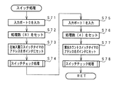
図17は、主基板31におけるCPU56が実行するメイン処理を示すフローチャートである。遊技機に対する電源が投入されると、メイン処理において、CPU56は、まず、必要な初期設定を行う。
【0133】
初期設定処理において、CPU56は、まず、割込禁止に設定する(ステップS1)。次に、割込モードを割込モード2に設定し(ステップS2)、スタックポインタにスタックポインタ指定アドレスを設定する(ステップS3)。そして、内蔵デバイスレジスタの初期化を行う(ステップS4)。また、内蔵デバイス(内蔵周辺回路)であるCTC(カウンタ/タイマ)およびPIO(パラレル入出力ポート)の初期化(ステップS5)を行った後、RAMをアクセス可能状態に設定する(ステップS6)。
【0134】
この実施の形態で用いられているCPU56には、マスク可能な割込(INT)のモードとして以下の3種類のモードが用意されている。なお、マスク可能な割込が発生すると、CPU56は、自動的に割込禁止状態に設定するとともに、プログラムカウンタの内容をスタックにセーブする。
【0135】
割込モード0:割込要求を行った内蔵デバイスがRST命令(1バイト)またはCALL命令(3バイト)をCPUの内部データバス上に送出する。よって、CPU56は、RST命令に対応したアドレスまたはCALL命令で指定されるアドレスの命令を実行する。リセット時に、CPU56は自動的に割込モード0になる。よって、割込モード1または割込モード2に設定したい場合には、初期設定処理において、割込モード1または割込モード2に設定するための処理を行う必要がある。
【0136】
割込モード1:割込が受け付けられると、常に0038(h)番地に飛ぶモードである。
【0137】
割込モード2:CPU56の特定レジスタ(Iレジスタ)の値(1バイト)と内蔵デバイスが出力する割込ベクタ(1バイト:最下位ビット0)から合成されるアドレスが、割込番地を示すモードである。すなわち、割込番地は、上位アドレスが特定レジスタの値とされ下位アドレスが割込ベクタとされた2バイトで示されるアドレスである。従って、任意の(飛び飛びではあるが)偶数番地に割込処理を設置することができる。各内蔵デバイスは割込要求を行うときに割込ベクタを送出する機能を有している。
【0138】
よって、割込モード2に設定されると、各内蔵デバイスからの割込要求を容易に処理することが可能になり、また、プログラムにおける任意の位置に割込処理を設置することが可能になる。さらに、割込モード1とは異なり、割込発生要因毎のそれぞれの割込処理を用意しておくことも容易である。上述したように、この実施の形態では、初期設定処理のステップS2において、CPU56は割込モード2に設定される。
【0139】
次いで、CPU56は、電源断時にバックアップRAM領域のデータ保護処理(例えばパリティデータの付加等の停電発生NMI処理)が行われたか否か確認する(ステップS7)。この実施の形態では、不測の電源断が生じた場合には、バックアップRAM領域のデータを保護するための処理が行われている。そのような保護処理が行われていた場合をバックアップありとする。バックアップなしを確認したら、CPU56は初期化処理を実行する。
【0140】
この実施の形態では、バックアップRAM領域にバックアップデータがあるか否かは、電源断時にバックアップRAM領域に設定されるバックアップフラグの状態によって確認される。この例では、図18に示すように、バックアップフラグ領域に「55H」が設定されていればバックアップあり(オン状態)を意味し、「55H」以外の値が設定されていればバックアップなし(オフ状態)を意味する。
【0141】
バックアップありを確認したら、CPU56は、バックアップRAM領域のデータチェック(この例ではパリティチェック)を行う。
【0142】
図19は、ステップS8のパリティチェック処理の一例を示すフローチャートである。パリティチェック処理では、CPU56は、まず、RAM55におけるバックアップパリティデータ領域に設定されているデータが「00」であるか否か確認する(ステップS8a)。バックアップパリティデータ領域については後で詳しく説明する。バックアップパリティデータ領域に設定されているデータが「00」でなければ、パリティ診断(チェックサム確認)を行う(ステップS8b)。そして、チェックサム確認の結果が正当であれば(ステップS8c)、CPU56は、後述する停電復旧処理を実行する(ステップS9)。また、チェックサム確認の結果が正当でなければ、または、バックアップパリティデータ領域に設定されているデータが「00」であった場合には、通常の初期化処理を実行する(ステップS11〜S15)。
【0143】
不測の電源断が生じた後に復旧した場合には、バックアップRAM領域のデータは保存されていたはずであるから、チェック結果は正常になる。チェック結果が正常でない場合には、内部状態を電源断時の状態に戻すことができないので、停電復旧時でない電源投入時に実行される初期化処理を実行する。
【0144】
チェック結果が正常であれば(ステップS8)、CPU56は、遊技制御手段の内部状態と表示制御手段等の電気部品制御手段の制御状態を電源断時の状態に戻すための遊技状態復旧処理を行う(ステップS9)。そして、バックアップRAM領域に保存されていたPC(プログラムカウンタ)の退避値がPCに設定され、そのアドレスに復帰する。
【0145】
なお、この実施の形態では、ステップS7でバックアップデータの有無が確認された後、バックアップデータが存在する場合にステップS8でバックアップ領域のチェックが行われたが、逆に、バックアップ領域のチェック結果が正常であったことが確認された後、バックアップデータの有無の確認を行うようにしてもよい。また、バックアップデータの有無の確認、またはバックアップ領域のチェックの何れか一方の確認を行うことによって、停電復旧処理を実行するか否かを判定してもよい。
【0146】
また、例えば停電復旧処理を実行するか否か判断する場合のパリティチェック(ステップS8)の際に、すなわち、遊技状態を復旧するか否か判断する際に、保存されていたRAMデータにおける特別プロセスフラグ等や始動入賞記憶数データによって、遊技機が遊技待機状態(図柄変動中でなく、大当り遊技中でなく、確変中でなく、また、始動入賞記憶がない状態)であることが確認されたら、遊技状態復旧処理を行わずに初期化処理を実行するようにしてもよい。
【0147】
以上のように、この実施の形態では、電力供給開始時に、電力供給停止時にバックアップRAM領域に記憶されたチェックデータ(チェックサムデータ)にもとづいて、初期化処理を行うか遊技状態復旧処理を行うかを決定するように構成したので、停電等の不測の電源断が発生したときに必要なデータを確実に保存することができ、さらに、保存されていたデータを電源復帰後に確実に活用することができる。
【0148】
なお、上述した実施の形態では、チェックサム確認の結果が正当でなかった場合には通常の初期化処理を実行するようにしていたが、チェックサム確認の結果が正当でなかった場合であっても初期化処理を行わないようにしてもよい。
【0149】
例えば、チェックサム確認の結果が正当でなかった場合に、初期化処理を実行することなく、バックアップRAMの記憶内容を修復したあと、遊技状態復旧処理を行うようにすればよい。この場合、データの修復は、例えば、誤り訂正符号(例えば、ランダム誤り対策に用いられるハミング符号、バースト誤り対策に用いられるFire符号など、誤り特性に合わせて選択するようにすればよい)を用いて、変化したビットを検出して訂正するようにすればよい。
【0150】
また、例えば、チェックサム確認の結果が正当でなかった場合に、初期化処理を実行することなく、バックアップRAMの記憶内容に異常が発生していることを報知するようにしてもよい。この場合、異常の報知は、所定の制御によって、例えば、異常が発生したことを可変表示装置9に表示し、スピーカ27から異常が発生したことを示す音声を出力し、ランプ制御基板35が制御する異常を報知するためのランプを点灯し、あるいはエラー表示用LED374に異常を示す所定の表示を行うようにすればよい。また、バックアップRAMの記憶内容に異常が発生していることを示す所定の信号を、情報出力回路64などを介して管理コンピュータに出力するようにしてもよい。
【0151】
初期化処理では、CPU56は、まず、RAMクリア処理を行う(ステップS11)。また、所定の作業領域(例えば、普通図柄判定用乱数カウンタ、普通図柄判定用バッファ、特別図柄左中右図柄バッファ、払出コマンド格納ポインタなど)に初期値を設定する初期値設定処理も行われる。さらに、サブ基板(ランプ制御基板35、払出制御基板37、音声制御基板70、図柄制御基板80)を初期化するための処理を実行する(ステップS13)。サブ基板を初期化する処理とは、例えば初期設定コマンドを送出する処理である。
【0152】
そして、2ms毎に定期的にタイマ割込がかかるようにCPU56に設けられているCTCのレジスタの設定が行われる(ステップS14)。すなわち、初期値として2msに相当する値が所定のレジスタ(時間定数レジスタ)に設定される。そして、初期設定処理のステップS1において割込禁止とされているので、初期化処理を終える前に割込が許可される(ステップS15)。
【0153】
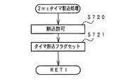
この実施の形態では、CPU56の内蔵CTCが繰り返しタイマ割込を発生するように設定される。この実施の形態では、繰り返し周期は2msに設定される。そして、タイマ割込が発生すると、図20に示すように、CPU56は、例えばタイマ割込が発生したことを示すタイマ割込フラグをセットする(ステップS12)。
【0154】
初期化処理の実行(ステップS11〜S15)が完了すると、メイン処理で、タイマ割込が発生したか否かの監視(ステップS17)の確認が行われるループ処理に移行する。なお、ループ内では、表示用乱数更新処理(ステップS16)も実行される。
【0155】
CPU56は、ステップS17において、タイマ割込が発生したことを認識すると、ステップS21〜S31の遊技制御処理を実行する。遊技制御処理において、CPU56は、まず、スイッチ回路58を介して、ゲートセンサ12、始動口センサ17、カウントセンサ23および入賞口スイッチ19a,19b,24a,24b等のスイッチの状態を入力し、それらの状態判定を行う(スイッチ処理:ステップS21)。
【0156】
次いで、パチンコ遊技機1の内部に備えられている自己診断機能によって種々の異常診断処理が行われ、その結果に応じて必要ならば警報が発せられる(エラー処理:ステップS22)。
【0157】
次に、遊技制御に用いられる大当り判定用の乱数等の各判定用乱数を示す各カウンタを更新する処理を行う(ステップS23)。CPU56は、さらに、停止図柄の種類を決定する乱数等の表示用乱数を更新する処理を行う(ステップS24)。
【0158】
さらに、CPU56は、特別図柄プロセス処理を行う(ステップS25)。特別図柄プロセス制御では、遊技状態に応じてパチンコ遊技機1を所定の順序で制御するための特別図柄プロセスフラグに従って該当する処理が選び出されて実行される。そして、特別図柄プロセスフラグの値は、遊技状態に応じて各処理中に更新される。また、普通図柄プロセス処理を行う(ステップS26)。普通図柄プロセス処理では、7セグメントLEDによる可変表示器10を所定の順序で制御するための普通図柄プロセスフラグに従って該当する処理が選び出されて実行される。そして、普通図柄プロセスフラグの値は、遊技状態に応じて各処理中に更新される。
【0159】
次いで、CPU56は、特別図柄に関する表示制御コマンドをRAM55の所定の領域に設定して表示制御コマンドを送出する処理を行う(特別図柄コマンド制御処理:ステップS27)。また、普通図柄に関する表示制御コマンドをRAM55の所定の領域に設定して表示制御コマンドを送出する処理を行う(普通図柄コマンド制御処理:ステップS28)。
【0160】
さらに、CPU56は、例えばホール管理用コンピュータに供給される大当り情報、始動情報、確率変動情報などのデータを出力する情報出力処理を行う(ステップS29)。
【0161】
また、CPU56は、所定の条件が成立したときにソレノイド回路59に駆動指令を行う(ステップS30)。ソレノイド回路59は、駆動指令に応じてソレノイド16,21を駆動し、可変入賞球装置15または開閉板20を開状態または閉状態とする。
【0162】
そして、CPU56は、各入賞口への入賞を検出するためのスイッチ17,23,19a,19b,24a,24bの検出出力にもとづく賞球数の設定などを行う賞球処理を実行する(ステップS31)。具体的には、入賞検出に応じて払出制御基板37に払出制御コマンドを出力する。払出制御基板37に搭載されている払出制御用CPU371は、払出制御コマンドに応じて球払出装置97を駆動する。
【0163】
以上の制御によって、この実施の形態では、遊技制御処理は2ms毎に起動されることになる。なお、この実施の形態では、タイマ割込処理では例えば割込が発生したことを示すフラグのセットのみがなされ、遊技制御処理はメイン処理において実行されるが、タイマ割込処理で遊技制御処理を実行してもよい。
【0164】
また、メイン処理には遊技制御処理に移行すべきか否かを判定する処理が含まれ、CPU56の内部タイマが定期的に発生するタイマ割込にもとづくタイマ割込処理で遊技制御処理に移行すべきか否かを判定するためのフラグのセット等がなされるので、遊技制御処理の全てが確実に実行される。つまり、遊技制御処理の全てが実行されるまでは、次回の遊技制御処理に移行すべきか否かの判定が行われないので、遊技制御処理中の全ての各処理が実行完了することは保証されている。
【0165】
以上に説明したように、この実施の形態では、CTCやPIOを内蔵するCPU56に対して、初期設定処理で割込モード2が設定される。従って、内蔵CTCを用いた定期的なタイマ割込処理を容易に実現できる。また、タイマ割込処理をプログラム上の任意の位置に設置できる。また、内蔵PIOを用いたスイッチ検出処理等を容易に割込処理で実現できる。その結果、プログラム構成が簡略化され、プログラム開発工数が低減する等の効果を得ることができる。
【0166】
なお、CTCおよびPIOの設定(ステップS5)が完了した後に、IEO/SCLK0端子から出力されるクロック信号の周波数を決めるための内部レジスタの設定を行ってもよい。その際、クロック信号の周波数は、遊技制御処理の起動周期である2msに応じた周波数とされる。そのような設定を行うと、IEO/SCLK0端子から、遊技制御処理の起動周期に応じた周波数のクロック信号がCPU56から外部出力される。すると、CPU56の外部において遊技制御処理の起動周期に対応した信号を観測することができる。よって、そのような信号を用いて、遊技機外部においてCPU56による遊技制御処理をシミュレーションしたり、CPU56の動作状況を試験したりすることが容易になる。
【0167】
次に、メイン処理におけるスイッチ処理(ステップS21)の具体例を説明する。この実施の形態では、検出信号のオン状態が所定時間継続すると、確かにスイッチがオンしたと判定されスイッチオンに対応した処理が開始される。所定時間を計測するために、スイッチタイマが用いられる。スイッチタイマは、バックアップRAM領域に形成された1バイトのカウンタであり、検出信号がオン状態を示している場合に2ms毎に+1される。図21に示すように、スイッチタイマは検出信号の数Nだけ設けられている。この実施の形態ではN=12である。また、RAMにおいて、各スイッチタイマのアドレスは、入力ポートのビット配列順(図16に示された上から下への順)と同じ順序で並んでいる。
【0168】
図22は、遊技制御処理におけるステップS21のスイッチ処理の処理例を示すフローチャートである。なお、スイッチ処理は、図17に示すように遊技制御処理において最初に実行される。スイッチ処理において、CPU56は、まず、入力ポート0に入力されているデータを入力する(ステップS71)。次いで、処理数として「8」を設定し(ステップS72)、入賞口スイッチ24aのためのスイッチタイマのアドレスをポインタにセットする(ステップS73)。そして、スイッチチェック処理サブルーチンをコールする(ステップS74)。
【0169】
図23は、スイッチチェック処理サブルーチンを示すフローチャートである。スイッチチェック処理サブルーチンにおいて、CPU56は、ポート入力データ、この場合には入力ポート0からの入力データを「比較値」として設定する(ステップS81)。また、クリアデータ(00)をセットする(ステップS82)。そして、ポインタ(スイッチタイマのアドレスが設定されている)が指すスイッチタイマをロードするとともに(ステップS83)、比較値を右(上位ビットから下位ビットへの方向)にシフトする(ステップS84)。比較値には入力ポート0のデータ設定がされている。そして、この場合には、入賞口スイッチ24aの検出信号がキャリーフラグに押し出される。
【0170】
キャリーフラグの値が「1」であれば(ステップS85)、すなわち入賞口スイッチ24aの検出信号がオン状態であれば、スイッチタイマの値を1加算する(ステップS87)。加算後の値が0でなければ加算値をスイッチタイマに戻す(ステップS88,S89)。加算後の値が0になった場合には加算値をスイッチタイマに戻さない。すなわち、スイッチタイマの値が既に最大値(255)に達している場合には、それよりも値を増やさない。
【0171】
キャリーフラグの値が「0」であれば、すなわち入賞口スイッチ24aの検出信号がオフ状態であれば、スイッチタイマにクリアデータをセットする(ステップS86)。すなわち、スイッチがオフ状態であれば、スイッチタイマの値が0に戻る。
【0172】
その後、CPU56は、ポインタ(スイッチタイマのアドレス)を1加算するとともに(ステップS90)、処理数を1減算する(ステップS91)。処理数が0になっていなければステップS82に戻る。そして、ステップS82〜S92の処理が繰り返される。
【0173】
ステップS82〜S92の処理は、処理数分すなわち8回繰り返され、その間に、入力ポート0の8ビットに入力されるスイッチの検出信号について、順次、オン状態かオフ状態か否かのチェック処理が行われ、オン状態であれば、対応するスイッチタイマの値が1増やされる。
【0174】
CPU56は、スイッチ処理のステップS75において、入力ポート1に入力されているデータを入力する。次いで、処理数として「4」を設定し(ステップS76)、賞球カウントスイッチ301Aのためのスイッチタイマのアドレスをポインタにセットする(ステップS77)。そして、スイッチチェック処理サブルーチンをコールする(ステップS78)。
【0175】
スイッチチェック処理サブルーチンでは、上述した処理が実行されるので、ステップS82〜S92の処理が、処理数分すなわち4回繰り返され、その間に、入力ポート1の4ビットに入力されるスイッチの検出信号について、順次、オン状態かオフ状態か否かのチェック処理が行われ、オン状態であれば、対応するスイッチタイマの値が1増やされる。
【0176】
なお、この実施の形態では、遊技制御処理が2ms毎に起動されるので、スイッチ処理も2msに1回実行される。従って、スイッチタイマは、2ms毎に+1される。
【0177】
図24〜図26は、遊技制御処理におけるステップS31の賞球処理の一例を示すフローチャートである。この実施の形態では、賞球処理では、入賞口スイッチ19a,19b,24a,24b、カウントスイッチ23および始動口スイッチ17が確実にオンしたか否か判定されるとともに、オンしたら所定の払出制御コマンドが払出制御基板37に送出されるように制御し、また、満タンスイッチ48および球切れスイッチ187が確実にオンしたか否か判定されるとともに、オンしたら所定の払出制御コマンドが払出制御基板37に送出されるように制御する等の処理が行われる。
【0178】
賞球処理において、CPU56は、入力判定値テーブルのオフセットとして「0」を設定し(ステップS121)、スイッチタイマのアドレスのオフセットとして「0」を設定する(ステップS122)。入力判定値テーブルのオフセット「0」は、入力判定値テーブルの最初のデータを使用することを意味する。また、各スイッチタイマは、図16に示された入力ポートのビット順と同順に並んでいるので、スイッチタイマのアドレスのオフセット「0」は入賞口スイッチ24aに対応したスイッチタイマが指定されることを意味する。また、繰り返し数として「4」をセットする(ステップS123)。そして、スイッチオンチェックルーチンがコールされる(ステップS124)。
【0179】
入力判定値テーブルとは、各スイッチについて、連続何回のオンが検出されたら確かにスイッチがオンしたと判定するための判定値が設定されているROM領域である。入力判定値テーブルの構成例は図29に示されている。図29に示すように、入力判定値テーブルには、上から順に、すなわちアドレス値が小さい領域から順に、「2」、「50」、「250」、「30」、「250」、「1」の判定値が設定されている。また、スイッチオンチェックルーチンでは、入力判定値テーブルの先頭アドレスとオフセット値とで決まるアドレスに設定されている判定値と、スイッチタイマの先頭アドレスとオフセット値とで決まるスイッチタイマの値とが比較され、一致した場合には、例えばスイッチオンフラグがセットされる。
【0180】
スイッチオンチェックルーチンの一例が図27に示されている。スイッチオンチェックルーチンにおいて、CPU56は、入力判定値テーブル(図29参照)の先頭アドレスを設定する(ステップS101)。そして、そのアドレスにオフセットを加算し(ステップS102)、加算後のアドレスからスイッチオン判定値をロードする(ステップS103)。
【0181】
次いで、CPU56は、スイッチタイマの先頭アドレスを設定し(ステップS104)、そのアドレスにオフセットを加算し(ステップS105)、加算後のアドレスからスイッチタイマの値をロードする(ステップS106)。各スイッチタイマは、図16に示された入力ポートのビット順と同順に並んでいるので、スイッチに対応したスイッチタイマの値がロードされる。
【0182】
そして、CPU56は、ロードしたスイッチタイマの値とスイッチオン判定値とを比較する(ステップS107)。それらが一致すれば、スイッチオンフラグをセットする(ステップS108)。
【0183】
この場合には、スイッチオンチェックルーチンにおいて、入賞口スイッチ24aに対応するスイッチタイマの値がスイッチオン判定値「2」に一致していればスイッチオンフラグがセットされる(ステップS125)。スイッチオンフラグがセットされたら、10個カウンタが1加算される(ステップS126)。スイッチチェックオンルーチンは、スイッチタイマのアドレスのオフセットが更新されつつ(ステップS129)、最初に設定された繰り返し数分だけ実行されるので(ステップS127,S128)、結局、入賞口スイッチ19a,19b,24a,24bについて、対応するスイッチタイマの値がスイッチオン判定値「2」と比較されることになる。なお、10個カウンタとは、景品としての10個の遊技球払出の回数を示すカウンタである。
【0184】
次に、CPU56は、入力判定値テーブルのオフセットとして「0」を設定し(ステップS130)、スイッチタイマのアドレスのオフセットとして「4」を設定する(ステップS131)。入力判定値テーブルのオフセット「0」は、入力判定値テーブルの最初のデータを使用することを意味する。また、各スイッチタイマは、図16に示された入力ポートのビット順と同順に並んでいるので、スイッチタイマのアドレスのオフセット「4」は始動口スイッチ17に対応したスイッチタイマが指定されることを意味する。そして、スイッチオンチェックルーチンがコールされる(ステップS132)。
【0185】
スイッチオンチェックルーチンにおいて、始動口スイッチ17に対応するスイッチタイマの値がスイッチオン判定値「2」に一致していればスイッチオンフラグがセットされるので(ステップS133)、6個カウンタが1加算される(ステップS134)。なお、6個カウンタとは、景品としての6個の遊技球払出の回数を示すカウンタである。
【0186】
次いで、CPU56は、入力判定値テーブルのオフセットとして「0」を設定し(ステップS135)、スイッチタイマのアドレスのオフセットとして「5」を設定する(ステップS136)。入力判定値テーブルのオフセット「0」は、入力判定値テーブルの最初のデータを使用することを意味する。また、各スイッチタイマは、図16に示された入力ポートのビット順と同順に並んでいるので、スイッチタイマのアドレスのオフセット「5」はカウントスイッチ23に対応したスイッチタイマが指定されることを意味する。そして、スイッチオンチェックルーチンがコールされる(ステップS137)。
【0187】
スイッチオンチェックルーチンにおいて、カウントスイッチ23に対応するスイッチタイマの値がスイッチオン判定値「2」に一致していればスイッチオンフラグがセットされるので(ステップS138)、15個カウンタが1加算される(ステップS134)。なお、15個カウンタとは、景品としての15個の遊技球払出の回数を示すカウンタである。
【0188】
さらに、CPU56は、入力判定値テーブルのオフセットとして「1」を設定し(ステップS150)、スイッチタイマのアドレスのオフセットとして「9」を設定する(ステップS151)。入力判定値テーブルのオフセット「1」は、入力判定値テーブルの2番目のデータ「50」を使用することを意味する。また、各スイッチタイマは、図16に示された入力ポートのビット順と同順に並んでいるので、スイッチタイマのアドレスのオフセット「9」は満タンスイッチ48に対応したスイッチタイマが指定されることを意味する。そして、スイッチオンチェックルーチンがコールされる(ステップS152)。
【0189】
スイッチオンチェックルーチンにおいて、満タンスイッチ48に対応するスイッチタイマの値が満タンスイッチオン判定値「50」に一致していればスイッチオンフラグがセットされるので(ステップS153)、満タンフラグがセットされる(ステップS154)。なお、図25には明示されていないが、満タンスイッチ48に対応したスイッチタイマの値が0になると、満タンフラグはリセットされる。
【0190】
また、CPU56は、入力判定値テーブルのオフセットとして「2」を設定し(ステップS156)、スイッチタイマのアドレスのオフセットとして「0A(H)」を設定する(ステップS157)。入力判定値テーブルのオフセット「2」は、入力判定値テーブルの3番目のデータ「250」を使用することを意味する。また、各スイッチタイマは、図16に示された入力ポートのビット順と同順に並んでいるので、スイッチタイマのアドレスのオフセット「0A(H)」は球切れスイッチ187に対応したスイッチタイマが指定されることを意味する。そして、スイッチオンチェックルーチンがコールされる(ステップS158)。
【0191】
スイッチオンチェックルーチンにおいて、球切れスイッチ187に対応するスイッチタイマの値が球切れスイッチオン判定値「250」に一致していればスイッチオンフラグがセットされるので(ステップS159)、球切れフラグがセットされる(ステップS160)。なお、図25には明示されていないが、球切れスイッチ187に対応したスイッチオフタイマが用意され、その値が50になると、球切れフラグはリセットされる。
【0192】
そして、CPU56は、払出停止状態であるか否か確認する(ステップS201)。払出停止状態は、払出制御基板37に対して払出停止状態指定のコマンドを送出した後の状態である。払出停止状態でなければ、上述した球切れ状態フラグまたは満タンフラグがオンになったか否かを確認する(ステップS202)。
【0193】
いずれかがオン状態に変化したときには、払出停止状態指定に関するコマンド送信制御処理を行う(ステップS203)。コマンド送信制御処理では、払出制御コマンド用のコマンド送信テーブルに所定のデータが設定された後、払出制御コマンドの送出処理が実行される。なお、ステップS202において、いずれか一方のフラグが既にオン状態であったときに他方のフラグがオン状態になったときには、コマンド送信制御処理(ステップS203)は行われない。
【0194】
また、払出停止状態であれば、球切れ状態フラグおよび満タンフラグがともにオフ状態になったか否かを確認する(ステップS204)。ともにオフ状態となったときには、払出停止解除指定に関するコマンド送信制御処理を行う(ステップS205)。
【0195】
次いで、CPU56は、入賞に応じた賞球個数に関する払出制御コマンドをコマンド送信テーブルに設定し、設定内容に応じた払出制御コマンドを送出する制御を行う。まず、15個カウンタの値をチェックする(ステップS221)。上述したように、15個カウンタは、遊技球が大入賞口に入賞してカウントスイッチ23がオンするとカウントアップされる。15個カウンタの値が0でない場合には、15個の賞球個数指示に関するコマンド送信制御処理を行う(ステップS222)。コマンド送信制御処理では、払出制御コマンド用のコマンド送信テーブルに所定のデータが設定された後、払出制御コマンドの送出処理が実行される。また、15個カウンタの値を−1する(ステップS223)。さらに、総賞球数格納バッファの格納値に15を加算する(ステップS224)。
【0196】
総賞球数格納バッファは、払出制御手段に対して指示した賞球個数の累積値(ただし、払い出しがなされると減算される)が格納されるバッファであり、バックアップRAMに形成されている。
【0197】
15個カウンタの値が0であれば、10個カウンタの値をチェックする(ステップS225)。上述したように、10個カウンタは、遊技球が入賞口に入賞して入賞口スイッチ19a,19b,24a,24bがオンするとカウントアップされる。10個カウンタの値が0でない場合には、10個の賞球個数指示に関するコマンド送信制御処理を行う(ステップS226)。また、10個カウンタの値を−1する(ステップS227)。さらに、総賞球数格納バッファの格納値に10を加算する(ステップS228)。
【0198】
10個カウンタの値が0であれば、6個カウンタの値をチェックする(ステップS231)。上述したように、6個カウンタは、遊技球が始動入賞口に入賞して始動口スイッチ17がオンするとカウントアップされる。6個カウンタの値が0でない場合には、6個の賞球個数指示に関するコマンド送信制御処理を行う(ステップS232)。また、6個カウンタの値を−1する(ステップS233)。さらに、総賞球数格納バッファの格納値に6を加算する(ステップS234)。
【0199】
以上にようにして、遊技制御手段から払出制御基板37に賞球個数を指示する払出制御コマンドを出力しようとするときに、コマンド送信テーブルの設定が行われた後、コマンド送信テーブルに設定された払出制御コマンドが払出制御基板37に送出される。そして、賞球個数を指示する払出制御コマンドの送出が行われたときには、賞球払出中フラグをオンする(ステップS235)。また、賞球払出中フラグをオンしているときには(ステップS236)、球払出装置97から実際に払い出された賞球数を監視して総賞球数格納バッファの格納値を減算する賞球個数減算処理が行われる(ステップS237)。なお、賞球払出中フラグがオンからオフに変化したときには、ランプ制御基板35に対して、賞球ランプ51の点灯を指示するランプ制御コマンドが送出される。
【0200】
図28は、賞球個数減算処理の一例を示すフローチャートである。賞球個数減算処理において、CPU56は、まず、総賞球数格納バッファの格納値をロードする(ステップS241)。そして、格納値が0であるか否か確認する(ステップS242)。0であれば処理を終了する。
【0201】
0でなければ、賞球カウントスイッチ用のスイッチタイマをロードし(ステップS243)、ロード値とオン判定値(この場合は「2」)とを比較する(ステップS244)。一致したら(ステップS245)、賞球カウントスイッチ301Aが確かにオンしたとして、すなわち、確かに1個の遊技球が球払出装置97から払い出されたとして、総賞球数格納バッファの格納値を1減算する(ステップS246)。
【0202】
また、賞球情報カウンタの値を+1する(ステップS247)。そして、賞球情報カウンタの値が10以上であれば(ステップS248)、賞球情報出力カウンタの値を+1するとともに(ステップS249)、賞球情報カウンタの値を−10する(ステップS250)。なお、賞球情報出力カウンタの値は、図17に示されたメイン処理における情報出力処理(ステップS29)で参照され、その値が1以上であれば、賞球信号として1パルスが出力される。よって、この実施の形態では、10個の遊技球が賞球として払い出される度に、1つの賞球信号が遊技機外部に出力される。
【0203】
そして、総賞球数格納バッファの格納値が0になったら(ステップS251)、賞球払出中フラグをクリアし(ステップS252)、賞球残数がないことを報知するために、ランプ制御コマンド用のコマンド送信テーブルに賞球ランプ51の消灯を示すコマンドデータを設定した後(ステップS253)、ランプ制御コマンドの送出処理を実行する(ステップS254)。
【0204】
図30〜図32は、電源基板910からの電源断信号に応じて実行されるマスク不能割込処理(電力供給停止時処理)の処理例を示すフローチャートである。
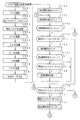
【0205】
電力供給停止時処理において、CPU56は、AFレジスタ(アキュミュレータとフラグのレジスタ)を所定のバックアップRAM領域に退避する(ステップS451)。また、割込フラグをパリティフラグにコピーする(ステップS452)。パリティフラグはバックアップRAM領域に形成されている。また、BCレジスタ、DEレジスタ、HLレジスタ、IXレジスタおよびスタックポインタをバックアップRAM領域に退避する(ステップS454〜S458)。なお、電源復旧時には、退避された内容にもとづいてレジスタ内容が復元され、パリティフラグの内容に応じて、割込許可状態/禁止状態の内部設定がなされる。
【0206】
次いで、この実施の形態では、所定期間、賞球カウントスイッチ301Aの検出信号をチェックする。そして、賞球カウントスイッチ301Aがオンしたら総賞球数バッファの内容を1減らす。
【0207】
なお、この実施の形態では、所定期間を計測するために、所定期間計測用カウンタが用いられる。所定期間計測用カウンタの値は、初期値mから、以下に説明するスイッチ検出処理のループ(S461から始まってS461に戻るループ)が1回実行される毎に−1され、その値が0になると、所定期間が終了したとする。検出処理のループでは、例外はあるがほぼ一定の処理が行われるので、ループの1周に要する時間のm倍の時間が、ほぼ所定期間に相当する。
【0208】
所定期間を計測するために、CPU56の内蔵タイマを用いてもよい。すなわち、スイッチ検出処理開始時に、内蔵タイマに所定値(所定期間に相当)を設定しておく。そして、スイッチ検出処理のループが1回実行される毎に、内蔵タイマのカウント値をチェックする。そして、カウント値が0になったら、所定期間が終了したとする。内蔵タイマの値が0になったことを検出するために内蔵タイマによる割込を用いることもできるが、この段階では制御内容(RAMに格納されている各値など)を変化させないように、割込を用いず、内蔵タイマのカウント値を読み出してチェックするようなプログラム構成の方が好ましい。
【0209】
また、所定期間は、遊技球が、球払出装置97から落下した時点から、賞球カウントスイッチ301Aに到達するまでの時間以上に設定される。球払出装置97から賞球カウントスイッチ301Aまでの距離をLとすると、その間の落下時間tは、t=√(2L/g)(g:重力加速度)になるので、所定期間は、それ以上に設定される。
【0210】
少なくとも、スイッチ検出処理が実行される所定期間では、賞球カウントスイッチ301Aが遊技球を検出できる状態でなければならない。そこで、この実施の形態では、図13に示されたように、電源基板910におけるコンバータIC922の入力側に比較的大容量の補助駆動電源としてのコンデンサ923が接続されている。よって、遊技機に対する電力供給停止時にも、ある程度の期間は+12V電源電圧がスイッチ駆動可能な範囲に維持され、賞球カウントスイッチ301Aが動作可能になる。その期間が、上記の所定期間以上になるように、コンデンサの容量が決定される。
【0211】
なお、入力ポートおよびCPU56も、コンバータIC922で作成される+5V電源で駆動されるので、電力供給停止時にも、比較的長い期間動作可能になっている。
【0212】
ステップS461において、2ms計測用カウンタに2msの時間に相当する初期値nが設定される。そして、2ms計測用カウンタの値が0になるまで(ステップS462)、2ms計測用カウンタの値が−1される(ステップS463)。
【0213】
2ms計測用カウンタの値が0になると、賞球カウントスイッチ301Aの検出信号の入力チェックが行われる。すなわち、図22および図23に示されたスイッチ処理およびスイッチチェック処理に類似した処理が行われる。具体的には、入力ポート1に入力されているデータを入力する(ステップS464)。次いで、クリアデータ(00)をセットする(ステップS465)。また、ポート入力データ、この場合には入力ポート1からの入力データを「比較値」として設定する(ステップS466)。さらに、賞球カウントスイッチ301Aのためのスイッチタイマのアドレスをポインタにセットする(ステップS467)。
【0214】
そして、ポインタ(スイッチタイマのアドレスが設定されている)が指すスイッチタイマをロードするとともに(ステップS468)、比較値を右(上位ビットから下位ビットへの方向)にシフトする(ステップS469)。比較値には入力ポート1のデータ設定されている。そして、この場合には、賞球カウントスイッチ301Aの検出信号がキャリーフラグに押し出される。
【0215】
キャリーフラグの値が「1」であれば(ステップS470)、すなわち賞球カウントスイッチ301Aの検出信号がオン状態であれば、スイッチタイマの値を1加算する(ステップS471)。キャリーフラグの値が「0」であれば、すなわち賞球カウントスイッチ301Aの検出信号がオフ状態であれば、スイッチタイマにクリアデータをセットする(ステップS472)。すなわち、スイッチがオフ状態であれば、スイッチタイマの値が0に戻る。
【0216】
そして、スイッチタイマの値が2になったときに(ステップS473)、総賞球数格納バッファの格納値を1減算するとともに(ステップS474)、賞球情報カウンタの値を+1する(ステップS475)。そして、賞球情報カウンタの値が10以上であれば(ステップS476)、賞球情報出力カウンタの値を+1するとともに(ステップS477)、賞球情報カウンタの値を−10する(ステップS478)。
【0217】
次いで、所定期間計測用カウンタの値を−1し(ステップS479)、その値が0になっていなければステップS461に戻る。
【0218】
以上の処理によって、所定期間内に賞球カウントスイッチ301Aがオンしたら、総賞球数格納バッファの値が−1される。バックアップRAMの内容を保存するための処理は、このようなスイッチ検出処理の後で行われるので、払出が完了した賞球について、必ず総賞球数格納バッファが−1される。従って、遊技球の払出に関して、保存される制御状態に矛盾が生じてしまうことが防止される。また、上記のスイッチ検出処理では、検出期間用カウンタを用いたタイマ処理が施されている。すなわち、2ms毎に賞球カウントスイッチ301Aの検出出力のチェックが行われ、2回連続してオン検出した場合に、賞球カウントスイッチ301Aが確実にオンしたと見なされる。従って、誤ってスイッチオン検出がなされてしまうことは防止される。また、スイッチ検出処理において、遊技機外部への賞球情報出力のための賞球情報出力回数カウンタの演算も行われるので、外部に出力される賞球情報と実際の払出賞球数とが食い違ってしまうようなこともない。
【0219】
なお、この実施の形態では、賞球カウントスイッチ301Aのみのスイッチ検出処理が行われたが、始動入賞口のスイッチや大入賞口に関連するV入賞スイッチ22やカウントスイッチについても同様のスイッチ検出処理を行ってもよい。また、他の入賞についても同様のスイッチ検出処理を行ってもよい。そのようなオンチェックも行う場合には、入賞口に遊技球が入賞した直後に停電が発生したような場合でも、その入賞が確実に検出され、保存される遊技状態に反映される。
【0220】
所定期間が経過すると(ステップS480)、すなわち、所定期間計測用カウンタの値が0になると、バックアップあり指定値(この例では「55H」)をバックアップフラグにストアする(ステップS481)。バックアップフラグはバックアップRAM領域に形成されている。次いで、パリティデータを作成する(ステップS482〜S491)。すなわち、まず、クリアデータ(00)をチェックサムデータエリアにセットし(ステップS482)、チェックサム算出開始アドレスをポインタにセットする(ステップS483)。また、チェックサム算出回数をセットする(ステップS484)。
【0221】
そして、チェックサムデータエリアの内容とポインタが指すRAM領域の内容との排他的論理和を演算する(ステップS485)。演算結果をチェックサムデータエリアにストアするとともに(ステップS486)、ポインタの値を1増やし(ステップS487)、チェックサム算出回数の値を1減算する(ステップS488)。ステップS485〜S488の処理が、チェックサム算出回数の値が0になるまで繰り返される(ステップS489)。
【0222】
チェックサム算出回数の値が0になったら、CPU56は、チェックサムデータエリアの内容の各ビットの値を反転する(ステップS490)。そして、反転後のデータをチェックサムデータエリアにストアする(ステップS491)。このデータが、電源投入時にチェックされるパリティデータとなる。
【0223】
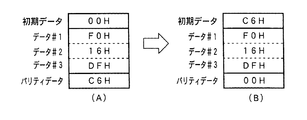
図33は、バックアップパリティデータ作成方法を説明するための説明図である。ただし、図33に示す例では、簡単のために、バックアップデータRAM領域のデータのサイズを3バイトとする。また、図33に示す例では、ステップS484でチェックサム算出回数として3がセットされるものとする。電源電圧低下にもとづく停電発生処理において、図33(A)に示すように、バックアップチェックデータ領域に、初期データ(この例では00H)が設定される。次に、「00H」とチェックサム算出開始アドレス(この例では「F0H」)の排他的論理和がとられ、その結果と次のポインタが指すRAM領域の内容(本例では「16H」)の排他的論理和がとられる。さらに、その結果と次のポインタが指すRAM領域の内容(本例では「DFH」)の排他的論理和がとられる。そして、その結果(この例では「39H」)を反転したデータ(この例では「C6H」)がバックアップパリティデータ領域に設定される。
【0224】
電源が再投入されたときには、チェックサム確認処理(ステップS8b)においてパリティ診断が行われるが、図33(B)はパリティ診断の例を示す説明図である。バックアップ領域の全データがそのまま保存されていれば、電源再投入時に、図33(A)に示すようなデータがバックアップ領域に設定されている。
【0225】
ステップS51の処理において、CPU56は、バックアップRAM領域のバックアップパリティデータ領域に設定されていたデータ(この例では「C6H」)を初期データとし、初期データを反転したデータ(この例では「39H」)を用いて、バックアップデータ領域の各データについて順次排他的論理和をとる処理を行う。バックアップ領域の全データがそのまま保存されていれば、最終的な演算結果は、「00H」、すなわちバックアップチェックデータ領域に設定されているデータと一致する。バックアップRAM領域内のデータにビット誤りが生じていた場合には、最終的な演算結果は「00H」にならない。
【0226】
よって、CPU56は、パリティチェック処理(チェックサム確認処理)において、最終的な演算結果とバックアップチェックデータ領域に設定されているデータとを比較して、一致すればパリティ診断正常とする。一致しなければ、パリティ診断異常とする。
【0227】
このように、この実施の形態では、図19に示されたパリティチェック処理において、バックアップパリティデータ領域に設定されていたデータが「00」でないときにチェックサム確認処理が行われ(ステップS9a,S9b)、バックアップパリティデータ領域に設定されていたデータが「00」である場合には停電復旧処理を行う。
【0228】
なお、この実施の形態では、チェックサム確認処理(ステップS8b)におけるパリティ診断において図33(B)に示すようにパリティ診断を行うようにしていたが、パリティ診断において、図33(A)と同様の処理を行うようにしてもよい。すなわち、パリティ診断において、パリティデータ作成のための演算処理と同じ演算処理を行うようにしてもよい。この場合、CPU56は、パリティチェック処理(チェックサム確認処理)において、最終的な演算結果とバックアップチェックデータ領域に設定されているデータ(この場合、「00」)とを比較して、一致すればパリティ診断正常とする。一致しなければ、パリティ診断異常とする。なお、パリティ診断においてもパリティデータ作成のときと同じ演算をおこなうので、初期データを設定する必要はない。
【0229】
次いで、CPU56は、RAMアクセスレジスタにアクセス禁止値を設定する(ステップS492)。以後、内蔵RAM55のアクセスができなくなる。電源電圧が低下していくときには、各種信号線のレベルが不安定になってRAM内容が化ける可能性があるが、このようにRAMアクセス禁止状態にしておけば、バックアップRAM内のデータが化けることはない。
【0230】
RAMアクセスレジスタにアクセス禁止値を設定すると、CPU56は、待機状態(ループ状態)に入る。従って、システムリセットされるまで、何もしない状態になる。
【0231】
何の処理もしない状態となるため、リセット管理回路940からのリセット信号によって外部から動作禁止状態にされる前に、内部的に動作停止状態になる。よって、電源断時に確実にCPU56は動作停止する。その結果、上述したRAMアクセス禁止の制御および動作停止制御によって、電源電圧が低下していくことに伴って生ずる可能性がある異常動作に起因するRAMの内容破壊等を確実に防止することができる。
【0232】
待機状態において、電源基板910から復帰信号が主基板31に供給されると、CPU56にリセットがかかるので、CPU56は、図17に示されたメイン処理の実行を開始することができる。その際、電源断信号が出力されたときに遊技状態が保存されているので、ステップS9の処理で遊技状態復旧処理が実行され、遊技制御は、電源断信号発生時の状態に戻り、その状態から遊技制御が続行される。
【0233】
なお、この実施の形態では、NMIに応じて電力供給停止時処理が実行されたが、電源断信号をCPU56のマスク可能端子に接続し、マスク可能割込処理によって電力供給停止時処理を実行してもよい。また、電源断信号を入力ポートに入力し、入力ポートのチェック結果に応じて電力供給停止時処理を実行してもよい。
【0234】
また、この実施の形態では、電源断信号に応じて起動される処理の最初にレジスタの保存処理が行われたが、スイッチ検出処理においてレジスタを使用しない場合には、スイッチ検出処理の実行後に、すなわち、バックアップフラグの設定とチェックサムの算出の処理の前にレジスタ保存処理を行うことができる。その場合には、レジスタ保存処理、バックアップフラグ設定処理およびチェックサム算出処理を電力供給停止時処理と見なすことができる。さらに、スイッチ検出処理において幾つかのレジスタを使用する場合であっても、使用しないレジスタについては、バックアップフラグの設定とチェックサムの算出の処理の前にレジスタ保存処理を行うことができる。
【0235】
図34は、払出検出手段からの検出信号の入力処理が実行される様子の一例を示すタイミング図である。この実施の形態では、電源断信号は、主基板31および払出制御基板37に入力され、主基板31のCPU56および払出制御用CPU371のNMI端子に入力される。主基板31のCPU56は、マスク不能割込処理によって、上述した電力供給停止時処理を実行する。
【0236】
図34に示すように、電源断信号がオン(この例ではハイレベルからローレベルに変化)するあたりで賞球払出が実行された場合、払出検出手段からの検出信号の入力処理が実行される所定期間内で賞球カウントスイッチ301Aがオンする。従って、電源断信号がオンするあたりで実行された球払出についても、電力供給停止時処理が実行される際に、総賞球数バッファに反映することができる。
【0237】
VSLの電圧値がさらに低下して所定値(この例では+9V)にまで低下すると、図14に示されたように電源基板710に搭載されているリセットIC651の出力がローレベルになり、CPU56がシステムリセット状態になる。なお、CPU56は、システムリセット状態とされる前に、電力供給停止時処理を完了している。
【0238】
VSLの電圧値がさらに低下してVcc(各種回路を駆動するための+5V)を生成することが可能な電圧を下回ると、各基板において各回路が動作できない状態となる。しかし、主基板31では、電力供給停止時処理が実行され、CPU56がシステムリセット状態とされている。
【0239】
なお、後述するように、払出制御基板37における払出制御用CPU371も、同様に電力供給停止時処理を行った後にシステムリセット状態になる。
【0240】
上記の実施の形態のパチンコ遊技機1は、始動入賞にもとづいて可変表示部9に可変表示される特別図柄の停止図柄が所定の図柄の組み合わせになると所定の遊技価値が遊技者に付与可能になる第1種パチンコ遊技機であったが、始動入賞にもとづいて可変表示される図柄の停止図柄が所定の図柄の組み合わせになると開放する所定の電動役物への入賞があると所定の権利が発生または継続する第3種パチンコ遊技機であっても、本発明を適用できる。
【0241】
以下、遊技状態復旧処理について説明する。
図35は、図17のステップS9に示された遊技状態復旧処理の一例を示すフローチャートである。この例では、CPU56は、バックアップRAMに保存されていた値を各レジスタに復元する(ステップS91)。そして、バックアップRAMに保存されていたデータにもとづいて停電時の遊技状態を確認して復帰させる。すなわち、バックアップRAMに保存されていたデータにもとづいて、ソレノイド回路59を介してソレノイド16やソレノイド21を駆動し、始動入賞口14や開閉板20の開閉状態の復旧を行う(ステップS92,S93)。また、電源断中でも保存されていた特別図柄プロセスフラグおよび普通図柄プロセスフラグの値に応じて、電源断時の特別図柄プロセス処理の進行状況および普通図柄プロセス処理の進行状況に対応した制御コマンドを、図柄制御基板80、ランプ制御基板35および音声制御基板70に送出する(ステップS94)。
【0242】
以上のように、遊技状態復旧処理では、復元された内部状態に応じて、各種電気部品の状態復元が行われるとともに、図柄制御基板80、ランプ制御基板35および音声制御基板70に対して、制御状態を電源断時の状態に戻すための制御コマンド(電源断時の制御状態を生じさせるための制御コマンド)が送出される。そのような制御コマンドは、一般に、電源断前に最後に送出された1つまたは複数の制御コマンドである。
【0243】
遊技状態を電源断時の状態に復帰させると、この実施の形態では、CPU56は、前回の電源断時の割込許可/禁止状態を復帰させるため、バックアップRAMに保存されていたパリティフラグの値を確認する(ステップS95)。パリティフラグがオフ状態であれば、割込許可設定を行う(ステップS96)。しかし、パリティフラグがオン状態であれば、そのまま(ステップS1で設定された割込禁止状態のまま)遊技状態復旧処理を終了する。パリティフラグがオン状態であるということは、図30におけるステップS452に示されたように、前回の電源断時に割込禁止状態であったことを意味する。従って、パリティフラグがオン状態である場合には、割込許可はなされない。
【0244】
この実施の形態では、上述した遊技状態復旧処理によって、以下のような状態復旧が可能である。
【0245】
始動入賞口14および大入賞口(開閉板20)の状態が復元される。表示制御手段によって制御される普通図柄の表示状態(可変表示器10の表示状態)は、電源断時に変動中であった場合を除いて復元される。表示制御手段によって制御される特別図柄の表示状態(可変表示部9の表示状態)は、電源断時に変動中であった場合を除いて復元される。さらに、可変表示部9に表示される背景やキャラクタは、特別図柄変動中および大当り遊技中であった場合を除いて復元される。
【0246】
特別図柄の変動中に電源断となった場合には、可変表示パターンの変動時間(例えば10秒)および既に実行した時間(例えば4秒)の情報がバックアップされる。そして、主基板31は、復旧時に、表示パターンを示す表示制御コマンドおよび停止図柄を示す表示制御コマンドを表示制御基板80に出力し、残り時間(上述の例では6秒)経過後に、図柄を停止させるため表示制御コマンドを出力する。従って、特別図柄の表示状態は、電源断時に特別図柄の変動中であった場合には、復旧時に、表示されていない残りの時間(上述の例では6秒)につき可変表示が実行される。なお、復旧時に表示制御基板80に対して出力される表示パターンを示す表示制御コマンドは、電源断前に出力された表示パターンを示す表示制御コマンドと同じものであってもよいが、「停電復旧中です」のような画像を表示させるためのコマンドとしてもよい。この場合、「停電復旧中です」の表示は、残りの時間(上述の例では6秒)表示される。なお、特別図柄の変動中に電源断となった場合の、普通図柄の表示状態にについても、上述と同様の制御が行われる。
【0247】
なお、大当り遊技中に電源断となった場合にも、上述した特別図柄の変動中に電源断となった場合と同様に、ラウンド中あるいはラウンド間のインターバルの残り時間について、復旧時に、表示、音、ランプ、ソレノイド21などを制御するが、主基板31は、表示制御基板80に対して電源断前に出力した確定時の図柄(停止図柄)を指定する表示制御コマンドを出力する。これにより、ラウンド中あるいはラウンド間の大当り図柄による演出が可能となり(大当り図柄で大当り演出する機種について)、また、大当り終了後の変動開始時に表示する図柄も表示制御基板80が認識することができる。
【0248】
ランプ制御手段が制御する装飾ランプ25、始動記憶表示器18、ゲート通過記憶表示器41、賞球ランプ51および球切れランプ52の表示状態が復元される。遊技効果ランプ・LED28a,28b,28cの表示状態は、特別図柄変動中および大当り遊技中であった場合を除いて復元される。ただし、電源断時に大当り遊技中であった場合には、各制御区間の最初の状態に復元可能である。各制御区間とは、例えば、大当り開始報知状態、大入賞口開放前状態、大入賞口開放中状態、大当り終了報知状態である。なお、特別図柄変動中に電源断となったあと復旧した場合には、上述した可変表示部9や可変表示装置10の表示制御と同様に、残り時間分だけ遊技効果ランプ・LED28a,28b,28cの表示状態を制御するようにしてもよいが、消灯または停電復旧時特有のパターンで点灯/点滅させるようにしてもよい。
【0249】
音声制御手段が制御する音発生状態は、特別図柄変動中および大当り遊技中であった場合を除いて復元される。ただし、電源断時に大当り遊技中であった場合には、各制御区間の最初の状態に復元可能である。なお、特別図柄変動中に電源断となったあと復旧した場合には、上述した可変表示部9や可変表示装置10の表示制御と同様に、残り時間分だけ音発生状態を制御するようにしてもよいが、無音または停電復旧時特有の音声パターン(例えば「停電復旧中です」との音声)を出力するようにしてもよい。
【0250】
なお、この実施の形態では、電源断からの復旧時に、主基板31の遊技制御手段から表示制御手段、ランプ制御手段および音声制御手段に対して状態復元のための制御コマンドが送出されるが、表示制御手段、ランプ制御手段および音声制御手段が電源バックアップされる場合には、主基板31からの制御コマンドを用いることなく、表示制御手段、ランプ制御手段および音声制御手段が独自に制御状態を復元するように構成してもよい。
【0251】
また、後述するように、払出制御基板37に搭載されている払出制御手段は、電源バックアップされているので、電源断からの復旧時に、賞球払出状態および球貸し制御状態は、電源断時の状態(電圧低下を検出したときから所定時間が経過したあとの状態)に復旧する。この実施の形態では、発射制御基板は払出制御手段に接続されているので、発射制御基板91における制御状態も同様に復元される。
【0252】
なお、上記の実施の形態では、遊技制御手段において、データ保存処理および復旧処理が行われる場合について説明したが、払出制御手段、音声制御手段、ランプ制御手段および表示制御手段におけるRAMの一部も電源バックアップされ、払出制御手段、表示制御手段、音制御手段およびランプ制御手段も、上述したような処理を行ってもよい。ただし、払出制御手段、表示制御手段、音制御手段およびランプ制御手段は、復旧時にコマンド送出処理を行う必要はない。
【0253】
次に、遊技制御手段以外の電気部品制御手段においてデータ保存処理および復旧処理が行われる場合の例として、払出制御手段においてデータ保存や復旧が行われる場合について説明する。
【0254】
図36は、この実施の形態における出力ポートの割り当てを示す説明図である。図36に示すように、出力ポートC(アドレス00H)は、払出モータ289に出力される駆動信号の出力ポートである。また、出力ポートD(アドレス01H)は、7セグメントLEDであるエラー表示LED374に出力される表示制御信号の出力ポートである。そして、出力ポートE(アドレス02H)は、振分ソレノイド310に出力される駆動信号、およびカードユニット50に対するEXS信号とPRDY信号とを出力するための出力ポートである。
【0255】
図37は、この実施の形態における入力ポートのビット割り当てを示す説明図である。図37に示すように、入力ポートA(アドレス06H)は、主基板31から送出された払出制御コマンドの8ビットの払出制御信号を取り込むための入力ポートである。また、入力ポートB(アドレス07H)のビット0〜2には、それぞれ、賞球カウントスイッチ301A、球貸しカウントスイッチ301B、モータ位置センサの検出信号が入力される。ビット3〜5には、カードユニット50からのBRDY信号、BRQ信号およびVL信号が入力される。
【0256】
図38は、払出制御用CPU371のメイン処理を示すフローチャートである。メイン処理では、払出制御用CPU371は、まず、必要な初期設定を行う。すなわち、払出制御用CPU371は、まず、割込禁止に設定する(ステップS701)。次に、割込モードを割込モード2に設定し(ステップS702)、スタックポインタにスタックポインタ指定アドレスを設定する(ステップS703)。また、払出制御用CPU371は、内蔵デバイスレジスタの初期化を行い(ステップS704)、CTCおよびPIOの初期化(ステップS705)を行った後に、RAMをアクセス可能状態に設定する(ステップS706)。
【0257】
この実施の形態では、内蔵CTCのうちの一つのチャネルがタイマモードで使用される。従って、ステップS704の内蔵デバイスレジスタの設定処理およびステップS705の処理において、使用するチャネルをタイマモードに設定するためのレジスタ設定、割込発生を許可するためのレジスタ設定および割込ベクタを設定するためのレジスタ設定が行われる。そして、そのチャネルによる割込がタイマ割込として用いられる。タイマ割込を例えば2ms毎に発生させたい場合は、初期値として2msに相当する値が所定のレジスタ(時間定数レジスタ)に設定される。
【0258】
なお、タイマモードに設定されたチャネル(この実施の形態ではチャネル3)に設定される割込ベクタは、タイマ割込処理の先頭番地に相当するものである。具体的は、Iレジスタに設定された値と割込ベクタとでタイマ割込処理の先頭番地が特定される。タイマ割込処理ではタイマ割込フラグがセットされ、メイン処理でタイマ割込フラグがセットされていることが検知されると、払出制御処理が実行される。すなわち、タイマ割込処理では、電気部品制御処理の一例である払出制御処理を実行するための設定がなされる。
【0259】
また、内蔵CTCのうちの他の一つのチャネル(この実施の形態ではチャネル2)が、遊技制御手段からの払出制御コマンド受信のための割込発生用のチャネルとして用いられ、そのチャネルがカウンタモードで使用される。従って、ステップS704の内蔵デバイスレジスタの設定処理およびステップS705の処理において、使用するチャネルをカウンタモードに設定するためのレジスタ設定、割込発生を許可するためのレジスタ設定および割込ベクタを設定するためのレジスタ設定が行われる。
【0260】
カウンタモードに設定されたチャネル(チャネル2)に設定される割込ベクタは、後述するコマンド受信割込処理の先頭番地に相当するものである。具体的は、Iレジスタに設定された値と割込ベクタとでコマンド受信割込処理の先頭番地が特定される。
【0261】
この実施の形態では、払出制御用CPU371でも割込モード2が設定される。従って、内蔵CTCのカウントダウンにもとづく割込処理を使用することができる。また、CTCが送出した割込ベクタに応じた割込処理開始番地を設定することができる。
【0262】
CTCのチャネル2(CH2)のカウントダウンにもとづく割込は、上述したタイマカウンタレジスタCLK/TRG2の値が「0」になったときに発生する割込である。従って、例えばステップS705において、特定レジスタとしてのタイマカウンタレジスタCLK/TRG2に初期値「1」が設定される。また、CTCのチャネル3(CH3)のカウントダウンにもとづく割込は、CPUの内部クロック(システムクロック)をカウントダウンしてレジスタ値が「0」になったら発生する割込であり、後述する2msタイマ割込として用いられる。具体的には、CH3のレジスタ値はシステムクロックの1/256周期で減算される。ステップS705において、CH3のレジスタには、初期値として2msに相当する値が設定される。
【0263】
CTCのCH2のカウントダウンにもとづく割込は、CH3のカウントダウンにもとづく割込よりも優先順位が高い。従って、同時にカウントダウンが生じた場合に、CH2のカウントダウンにもとづく割込、すなわち、コマンド受信割込処理の実行契機となる割込の方が優先される。
【0264】
次いで、払出制御用CPU371は、払出制御用のバックアップRAM領域にバックアップデータが存在しているか否かの確認を行う(ステップS707)。すなわち、例えば、主基板31のCPU56の処理と同様に、電源断時にセットされるバックアップフラグがセット状態になっているか否かによって、バックアップデータが存在しているか否か確認する。バックアップフラグがセット状態になっている場合には、バックアップデータありと判断する。
【0265】
バックアップありを確認したら、払出制御用CPU371は、バックアップRAM領域のデータチェック(この例ではパリティチェック)を行う。
【0266】
図39は、ステップS708のパリティチェック処理の一例を示すフローチャートである。パリティチェックでは、CPU56は、まず、RAM55におけるバックアップパリティデータ領域に設定されているデータが「00」であるか否か確認する(ステップS708a)。バックアップパリティデータ領域については後で詳しく説明する。バックアップパリティデータ領域に設定されているデータが「00」でなければ、パリティ診断(チェックサム確認)を行う(ステップS708b)。そして、チェックサム確認の結果が正当であれば(ステップS708c)、CPU56は、後述する停電復旧処理を実行する(ステップS709)。また、チェックサム確認の結果が正当でなければ、または、バックアップパリティデータ領域に設定されているデータが「00」であった場合には、通常の初期化処理を実行する(ステップS711〜S713)。
【0267】
不測の電源断が生じた後に復旧した場合には、バックアップRAM領域のデータは保存されていたはずであるから、チェック結果は正常になる。チェック結果が正常でない場合には、内部状態を電源断時の状態に戻すことができないので、停電復旧時でない電源投入時に実行される初期化処理を実行する。
【0268】
チェック結果が正常であれば(ステップS708)、払出制御用CPU371は、内部状態を電源断時の状態に戻すための払出状態復旧処理を行う(ステップS709)。そして、バックアップRAM領域に保存されていたPC(プログラムカウンタ)の指すアドレスに復帰する。
【0269】
以上のように、この実施の形態では、電力供給開始時に、電力供給停止時にバックアップRAM領域に記憶されたチェックデータ(チェックサムデータ)にもとづいて、初期化処理を行うか遊技状態復旧処理を行うかを決定するように構成したので、停電等の不測の電源断が発生したときに必要なデータを確実に保存することができ、さらに、保存されていたデータを電源復帰後に確実に活用することができる。
【0270】
なお、電源投入時に、変動データ記憶手段にバックアップデータが記憶されていない場合に実行される初期化処理と、パリティチェックの結果が不当なものであった場合に実行される初期化処理とは、プログラム上兼用されている。従って、停電等の不測の電源断が発生したときに必要なデータを確実に保存することができ、さらに保存されていたデータを電源復帰後に確実に活用することができるようにしても、プログラム容量はさほど増えない。
【0271】
また、上述した実施の形態では、チェックサム確認の結果が正当でなかった場合には通常の初期化処理を実行するようにしていたが、チェックサム確認の結果が正当でなかった場合であっても初期化処理を行わないようにしてもよい。
【0272】
例えば、チェックサム確認の結果が正当でなかった場合に、初期化処理を実行することなく、バックアップRAMの記憶内容を修復したあと、遊技状態復旧処理を行うようにすればよい。この場合、データの修復は、例えば、誤り訂正符号(例えば、ランダム誤り対策に用いられるハミング符号、バースト誤り対策に用いられるFire符号など、誤り特性に合わせて選択するようにすればよい)を用いて、変化したビットを検出して訂正するようにすればよい。
【0273】
また、例えば、チェックサム確認の結果が正当でなかった場合に、初期化処理を実行することなく、バックアップRAMの記憶内容に異常が発生していることを報知するようにしてもよい。この場合、異常の報知は、所定の制御によって、例えば、エラー表示用LED374に異常を示す所定の表示を行うようにすればよい。また、バックアップRAMの記憶内容に異常が発生していることを示す所定の信号を、情報出力回路64などを介して管理コンピュータに出力するようにしてもよい。
【0274】
初期化処理では、払出制御用CPU371は、まず、RAMクリア処理を行う(ステップS711)。そして、2ms毎に定期的にタイマ割込がかかるように払出制御用CPU371に設けられているCTCのレジスタの設定が行われる(ステップS712)。すなわち、初期値として2msに相当する値が所定のレジスタ(時間定数レジスタ)に設定される。そして、初期設定処理のステップS701において割込禁止とされているので、初期化処理を終える前に割込が許可される(ステップS713)。
【0275】
この実施の形態では、払出制御用CPU371の内蔵CTCが繰り返しタイマ割込を発生するように設定される。この実施の形態では、繰り返し周期は2msに設定される。そして、タイマ割込が発生すると、図40に示すように、払出制御用CPU371は、例えばタイマ割込が発生したことを示すタイマ割込フラグをセットする(ステップS721)。なお、図40には割込を許可することも明示されているが(ステップS720)、2msタイマ割込処理では、最初に割込許可状態に設定される。すなわち、2msタイマ割込処理中には割込許可状態になってので、INT信号の入力にもとづく払出制御コマンド受信処理を優先して実行することができる。
【0276】
払出制御用CPU371は、ステップS724において、タイマ割込フラグがセットされたことを検出するとステップS751以降の払出制御処理を実行する。以上の制御によって、この実施の形態では、払出制御処理は2ms毎に起動されることになる。なお、この実施の形態では、タイマ割込処理ではフラグセットのみがなされ、払出制御処理はメイン処理において実行されるが、タイマ割込処理で払出制御処理を実行してもよい。
【0277】
払出制御処理において、払出制御用CPU371は、まず、中継基板72を介して入力ポート372bに入力される賞球カウントスイッチ301A、球貸しカウントスイッチ301Bがオンしたか否かを判定する(スイッチ処理:ステップS751)。
【0278】
次に、払出制御用CPU371は、センサ(例えば、払出モータ289の回転数を検出するモータ位置センサ)からの信号入力状態を確認してセンサの状態を判定する等の処理を行う(入力判定処理:ステップS752)。払出制御用CPU371は、さらに、受信した払出制御コマンドを解析し、解析結果に応じた処理を実行する(コマンド解析実行処理:ステップS753)。
【0279】
次いで、払出制御用CPU371は、主基板31から払出停止指示コマンドを受信していたら払出停止状態に設定し、払出開始指示コマンドを受信していたら払出停止状態の解除を行う(ステップS754)。また、プリペイドカードユニット制御処理を行う(ステップS755)。
【0280】
次いで、払出制御用CPU371は、球貸し要求に応じて貸し球を払い出す制御を行う(ステップS756)。このとき、払出制御用CPU371は、振分ソレノイド310によって球振分部材311を球貸し側に設定する。
【0281】
さらに、払出制御用CPU371は、総合個数記憶に格納された個数の賞球を払い出す賞球制御処理を行う(ステップS757)。このとき、払出制御用CPU371は、振分ソレノイド310によって球振分部材311を賞球側に設定する。そして、出力ポート372cおよび中継基板72を介して球払出装置97の払出機構部分における払出モータ289に対して駆動信号を出力し、所定の回転数分払出モータ289を回転させる払出モータ制御処理を行う(ステップS758)。
【0282】
なお、この実施の形態では、払出モータ289としてステッピングモータが用いられ、それらを制御するために1−2相励磁方式が用いられる。従って、具体的には、払出モータ制御処理において、8種類の励磁パターンデータが繰り返し払出モータ289に出力される。また、この実施の形態では、各励磁パターンデータが4msずつ出力される。
【0283】
次いで、エラー検出処理が行われ、その結果に応じてエラー表示LED374に所定の表示を行う(エラー処理:ステップS759)。
【0284】
なお、出力ポートCは、払出制御処理における払出モータ制御処理(ステップS758)でアクセスされる。また、出力ポートDは、払出制御処理におけるエラー処理(ステップS759)でアクセスされる。そして、出力ポートEは、払出制御処理における球貸し制御処理(ステップS756)および賞球制御処理(ステップS757)でアクセスされる。
【0285】
図41は、払出制御用CPU371が内蔵するRAMの使用例を示す説明図である。この例では、バックアップRAM領域に、総合個数記憶(例えば2バイト)と貸し球個数記憶とがそれぞれ形成されている。総合個数記憶は、主基板31の側から指示された賞球払出個数の総数を記憶するものである。貸し球個数記憶は、未払出の球貸し個数を記憶するものである。
【0286】
このように、未払出の賞球個数と貸し球個数とが、所定期間はその内容を保持可能なバックアップRAM領域に記憶されるので、停電等の不測の電源断が生じても、所定期間内に電源復旧すれば、バックアップRAM領域に記憶される賞球処理および球貸し処理を続行できる。従って、遊技者に与えられる不利益を低減することができる。
【0287】
図42〜図44は、電源基板910からの電源断信号に応じて実行されるマスク不能割込処理の処理例を示すフローチャートである。この例では、NMIに応じて電力供給停止時処理が実行されるが、電源断信号を払出制御用CPU371のマスク可能端子に接続し、マスク可能割込処理によって電力供給停止時処理を実行してもよい。また、電源断信号を入力ポートに入力し、入力ポートのチェック結果に応じて電力供給停止時処理を実行してもよい。
【0288】
マスク不能割込処理において、払出制御用CPU371は、AFレジスタを所定のバックアップRAM領域に退避する(ステップS801)。また、割込フラグをパリティフラグにコピーする(ステップS802)。パリティフラグはバックアップRAM領域に形成されている。また、BCレジスタ、DEレジスタ、HLレジスタ、IXレジスタおよびスタックポインタをバックアップRAM領域に退避する(ステップS804〜808)。なお、電源復旧時には、退避された内容にもとづいてレジスタ内容が復元され、パリティフラグの内容に応じて、割込許可状態/禁止状態の内部設定がなされる。
【0289】
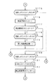
次いで、払出モータ289に出力される駆動信号をオフ状態にする(ステップS761)。よって、球払出装置97の駆動は停止する。その後、この実施の形態では、所定期間、払出検出手段としての賞球カウントスイッチ301A(賞遊技媒体検出手段に相当)および球貸しカウントスイッチ301B(貸出遊技媒体検出手段に相当)の検出信号をチェックする。そして、賞球カウントスイッチ301Aがオンしたら総合個数記憶の内容を1減らす。また、球貸しカウントスイッチ301Bがオンしたら貸し球個数記憶の内容を1減らす。
【0290】
なお、この実施の形態では、所定期間を計測するために、所定期間計測用カウンタが用いられる。所定期間計測用カウンタの値は、初期値mから、以下に説明するスイッチ検出処理のループ(S763から始まってS763に戻るループ)が1回実行される毎に−1され、その値が0になると、所定期間が終了したとする。検出処理のループでは、例外はあるがほぼ一定の処理が行われるので、ループの1周に要する時間のm倍の時間が、ほぼ所定期間に相当する。
【0291】
所定期間を計測するために、払出制御用CPU371の内蔵タイマを用いてもよい。すなわち、スイッチ検出処理開始時に、内蔵タイマに所定値(所定期間に相当)を設定しておく。そして、スイッチ検出処理のループが1回実行される毎に、内蔵タイマのカウント値をチェックする。そして、カウント値が0になったら、所定期間が終了したとする。内蔵タイマの値が0になったことを検出するために内蔵タイマによる割込を用いることもできるが、この段階では制御内容(RAMに格納されている各値など)を変化させないように、割込を用いず、内蔵タイマのカウント値を読み出してチェックするようなプログラム構成の方が好ましい。また、所定期間は、遊技球が、球払出装置97から落下した時点から、賞球カウントスイッチ301Aまたは球貸しカウントスイッチ301Bに到達するまでの時間以上に設定される。
【0292】
少なくとも、スイッチ検出処理が実行される所定期間では、賞球カウントスイッチ301Aおよび球貸しカウントスイッチ301Bが遊技球を検出できる状態でなければならない。そこで、この実施の形態では、図13に示されたように、電源基板910におけるコンバータIC922の入力側に比較的大容量の補助駆動電源としてのコンデンサ923が接続されている。よって、遊技機に対する電力供給停止時にも、ある程度の期間は+12V電源電圧がスイッチ駆動可能な範囲に維持され、賞球カウントスイッチ301Aおよび球貸しカウントスイッチ301Bが動作可能になる。その期間が、上記の所定期間以上になるように、コンデンサの容量が決定される。
【0293】
なお、入力ポートおよび払出制御用CPU371も、コンバータIC922で作成される+5V電源で駆動されるので、電力供給停止時にも、比較的長い期間動作可能になっている。
【0294】
さらに、この実施の形態では、賞球路と貸し球路とを切り換えるために振分ソレノイド310が用いられている。よって、図13に示されたコンデンサ923の容量は、少なくとも上記の所定期間の間、振分ソレノイド310も駆動できるような容量になっている。なお、コンデンサ923は、VSLの電源ラインと並列接続されているが、電源断信号に応じて遊技制御手段が他のソレノイド(大入賞口開閉用等)の駆動信号をオフ状態にしているので、電源断信号発生後では、コンデンサ923は、各ソレノイドのうちでは振分ソレノイド310のみを駆動できればよい。
【0295】
なお、この実施の形態で用いられているコンデンサ923は補助駆動電源の一つの例であるが、補助駆動電源として他のものを用いてもよい。少なくとも、上記の所定期間の間は、賞球カウントスイッチ301A、球貸しカウントスイッチ301B、振分ソレノイド310および払出制御用CPU371等の払出制御手段を駆動できるものであれば、他の態様の補助駆動電源を用いることができる。
【0296】
払出検出手段からの検出信号の入力処理(スイッチ検出処理)では、払出制御用CPU371は、まず、所定期間計測用カウンタに、所定期間に対応した値mを設定する(ステップS762)。そして、払出制御用CPU371は、所定期間計測用カウンタの値を−1し(ステップS763)、所定期間計測用カウンタの値を確認する(ステップS764)。その値が0であれば、スイッチ検出処理を終了し、制御状態を保存するための処理である電力供給停止時処理に移行する。
【0297】
所定期間計測用カウンタの値が0になっていなければ、賞球カウントスイッチオン中であるか否か確認する(ステップS765)。オン中であれば、検出期間用カウンタの値を1減らした後(ステップS766)、検出期間用カウンタの値が0になったか否か確認する(ステップS767)。0になっていれば、入力ポートを介して賞球カウントスイッチ301Aの検出信号を確認し(ステップS768)、オン状態を示していれば、賞球カウントスイッチ301Aが確実にオンしたとして、総合個数記憶の値を1減らす(ステップS769)。
【0298】
ステップS765で、賞球カウントスイッチオン中でないことを確認したら、入力ポートを介して賞球カウントスイッチ301Aの検出信号を確認し(ステップS770)、オン状態を示していれば、賞球カウントスイッチON中フラグをセットするとともに(ステップS771)、検出期間用カウンタに初期値nをセットする(ステップS772)。
【0299】
以上の処理によって、所定期間内に賞球カウントスイッチ301Aがオンしたら、総合個数記憶の値が−1される。バックアップRAMの内容を保存するための処理は、このようなスイッチ検出処理の後で行われるので、払出が完了した賞球について、必ず総合個数記憶が−1される。従って、遊技球の払出に関して、保存される制御状態に矛盾が生じてしまうことが防止される。また、上記のスイッチ検出処理では、検出期間用カウンタを用いたタイマ処理が施されている。すなわち、一度賞球カウントスイッチ301Aのオンが検出された後、所定時間(S763からS767に至りS763に戻るループにおける処理時間のn倍)の経過後にもオンが検出されないとスイッチオンと見なされない。従って、誤ってスイッチオン検出がなされてしまうことは防止される。
【0300】
なお、通常時のスイッチ処理(図38におけるステップS751)でも、誤検出防止用のタイマ処理が施されている。よって、そのような通常時のスイッチ処理をコールするようにしてもよい。また、ここでは、検出期間用カウンタを用いたタイマ処理が行われたが、所定期間の計測の場合にCPU内蔵タイマを用いてもよいのと同様、CPU内蔵タイマを用いてスイッチ検出処理におけるタイマ処理を実現してもよい。
【0301】
賞球カウントスイッチオン中でなく、かつ、賞球カウントスイッチ301Aのオン状態が検出できない場合には、球貸しカウントスイッチ301Bについてスイッチ検出処理を行う。すなわち、払出制御用CPU371は、球貸しカウントスイッチオン中であるか否か確認する(ステップS775)。オン中であれば、検出期間用カウンタの値を1減らした後(ステップS776)、検出期間用カウンタの値が0になったか否か確認する(ステップS777)。0になっていれば、入力ポートを介して球貸しカウントスイッチ301Bの検出信号を確認し(ステップS778)、オン状態を示していれば、球貸しカウントスイッチ301Bが確実にオンしたとして、貸し球個数記憶の値を1減らす(ステップS779)。
【0302】
ステップS775で、球貸しカウントスイッチオン中でないことを確認したら、入力ポートを介して球貸しカウントスイッチ301Bの検出信号を確認し(ステップS780)、オン状態を示していれば、球貸しカウントスイッチON中フラグをセットするとともに(ステップS781)、検出期間用カウンタに初期値nをセットする(ステップS782)。
【0303】
以上の処理によって、所定期間内に球貸しカウントスイッチ301Bがオンしたら、貸し球個数記憶の値が−1される。バックアップRAMの内容を保存するための処理は、このようなスイッチ検出処理の後で行われるので、払出が完了した貸し球について、必ず貸し球個数記憶が−1される。従って、遊技球の払出に関して、保存される制御状態に矛盾が生じてしまうことが防止される。また、上記のスイッチ検出処理では、検出期間用カウンタを用いたタイマ処理が施されている。すなわち、球貸しカウントスイッチ301Bのオンが所定時間以上継続しないとスイッチオンと見なされない。従って、誤ってスイッチオン検出がなされてしまうことは防止される。
【0304】
所定期間が経過すると(ステップS764)、払出制御用CPU371は、バックアップあり指定値(この例では「55H」)をバックアップフラグにストアする(ステップS809)。バックアップフラグはバックアップRAM領域に形成されている。
【0305】
次いで、主基板31のCPU56の処理と同様の処理を行ってパリティデータを作成しバックアップRAM領域に保存する(ステップS810〜S819)。
【0306】
図45は、バックアップパリティデータ作成方法を説明するための説明図である。ただし、図45に示す例では、簡単のために、バックアップデータRAM領域のデータのサイズを3バイトとする。また、図45に示す例では、ステップS812でチェックサム算出回数として3がセットされるものとする。電源電圧低下にもとづく停電発生処理において、図45(A)に示すように、バックアップチェックデータ領域に、初期データ(この例では00H)が設定される。次に、「00H」とチェックサム算出開始アドレス(この例では「F0H」)の排他的論理和がとられ、その結果と次のポインタが指すRAM領域の内容(本例では「16H」)の排他的論理和がとられる。さらに、その結果と次のポインタが指すRAM領域の内容(本例では「DFH」)の排他的論理和がとられる。そして、その結果(この例では「39H」)を反転したデータ(この例では「C6H」)がバックアップパリティデータ領域に設定される。
【0307】
電源が再投入されたときには、チェックサム確認処理(ステップS708b)においてパリティ診断が行われるが、図45(B)はパリティ診断の例を示す説明図である。バックアップ領域の全データがそのまま保存されていれば、電源再投入時に、図45(A)に示すようなデータがバックアップ領域に設定されている。
【0308】
ステップS708の処理において、払出制御用CPU371は、バックアップRAM領域のバックアップパリティデータ領域に設定されていたデータ(この例では「C6H」)を初期データとし、初期データを反転したデータ(この例では「39H」)を用いて、バックアップデータ領域の各データについて順次排他的論理和をとる処理を行う。バックアップ領域の全データがそのまま保存されていれば、最終的な演算結果は、「00H」、すなわちバックアップチェックデータ領域に設定されているデータと一致する。バックアップRAM領域内のデータにビット誤りが生じていた場合には、最終的な演算結果は「00H」にならない。
【0309】
よって、CPU56は、パリティチェック処理(チェックサム確認処理)において、最終的な演算結果とバックアップチェックデータ領域に設定されているデータとを比較して、一致すればパリティ診断正常とする。一致しなければ、パリティ診断異常とする。
【0310】
このように、この実施の形態では、図45に示されたパリティチェック処理において、バックアップパリティデータ領域に設定されていたデータが「00」でないときにチェックサム確認処理が行われ(ステップS708a,S708b)、バックアップパリティデータ領域に設定されていたデータが「00」である場合には停電復旧処理を行う。
【0311】
なお、この実施の形態では、チェックサム確認処理(ステップS708b)におけるパリティ診断において図45(B)に示すようにパリティ診断を行うようにしていたが、パリティ診断において、図45(A)と同様の処理を行うようにしてもよい。すなわち、パリティ診断において、パリティデータ作成のための演算処理と同じ演算処理を行うようにしてもよい。この場合、払出制御用CPU371は、パリティチェック処理(チェックサム確認処理)において、最終的な演算結果とバックアップチェックデータ領域に設定されているデータ(この場合、「00」)とを比較して、一致すればパリティ診断正常とする。一致しなければ、パリティ診断異常とする。なお、パリティ診断においてもパリティデータ作成のときと同じ演算をおこなうので、初期データを設定する必要はない。
【0312】
パリティデータを作成してバックアップRAM領域に保存すると、払出制御用CPU371は、RAMアクセスレジスタにアクセス禁止値を設定する(ステップS820)。以後、内蔵RAMのアクセスができなくなる。電源電圧が低下していくときには、各種信号線のレベルが不安定になってRAM内容が化ける可能性があるが、このようにRAMアクセス禁止状態にしておけば、バックアップRAM内のデータが化けることはない。
【0313】
以上のように、この実施の形態では、停電等の発生に応じて電源断信号が出力されたら、まず、球払出装置97の駆動を停止した後、所定期間、払出検出手段からの検出信号の入力処理が実行され、その後、払出制御状態を保存するための処理が行われる。従って、停電発生時に払出途中であった遊技球も、バックアップRAMの保存内容に反映される。
【0314】
すなわち、この実施の形態では、遊技機への電力供給停止時に制御状態をバックアップ記憶手段に保存するように構成した場合に、制御の矛盾等を生じさせないようにすることができる。
【0315】
RAMアクセスレジスタにアクセス禁止値を設定する処理が完了すると、払出制御用CPU371は、待機状態(ループ状態)に入る。従って、システムリセットされるまで、何もしない状態になる。
【0316】
何らの処理もしない状態になるので、リセット管理回路940からのリセット信号によって外部から動作禁止状態にされる前に、内部的に動作停止状態になる。よって、電源断時に確実に払出制御用CPU371は動作停止する。その結果、上述したRAMアクセス禁止の制御および動作停止制御によって、電源電圧が低下していくことに伴って生ずる可能性がある異常動作に起因するRAMの内容破壊等を確実に防止することができる。
【0317】
上述したように、電源の瞬断等に起因して電源断信号が発生した場合には、電源電圧は平常時の値に復旧し遊技機は制御可能な状態に戻る。そのような状況が発生したときには、電源基板910から復帰信号が払出基板37に供給される。復帰信号が入力されると、払出制御用CPU371にリセットがかかる。従って、払出制御用CPU371は、図38に示されたメイン処理の実行を開始することができる。その際、電源断信号が出力されたときに遊技状態が保存されているので、ステップS708の処理で払出状態復旧処理が実行され、払出制御は、電源断信号発生時の状態に戻り、その状態から払出制御が続行される。
【0318】
なお、ここでは、賞球カウントスイッチ301Aまたは球貸しカウントスイッチ301Bの検出信号がオン状態を示したらタイマ(検出期間用カウンタ)をセットし、タイマがタイムアップしたときにも検出信号がオン状態を示していたら、スイッチが確実にオンしたと判定したが、主基板31のCPU56と同様に、2msのタイマ(2ms計測用カウンタ)がタイムアップする毎に検出信号の判定を行うように構成してもよい。
【0319】
また、この実施の形態でも、電源断信号に応じて起動される処理の最初にレジスタの保存処理が行われたが、スイッチ検出処理においてレジスタを使用しない場合には、スイッチ検出処理の実行後に、すなわち、バックアップフラグの設定とチェックサムの算出の処理の前にレジスタ保存処理を行うことができる。その場合には、レジスタ保存処理、バックアップフラグ設定処理およびチェックサム算出処理を電力供給停止時処理と見なすことができる。さらに、スイッチ検出処理において幾つかのレジスタを使用する場合であっても、使用しないレジスタについては、バックアップフラグの設定とチェックサムの算出の処理の前にレジスタ保存処理を行うことができる。
【0320】
この実施の形態では、未払出の賞球および貸し球の総数が保存されるが、払出回数(例えば1回について25個)を記憶するというような他の保存方式を用いている場合であっても、電源断信号に応じて、所定期間は払出検出手段からの検出信号の入力処理が実行されるように構成されている場合には、保存される制御状態に矛盾が生じてしまうことが防止される。
【0321】
上述したように、上記の各実施の形態では、停電等の発生に応じて電源断信号が出力されたら、まず、払出装置の駆動を停止した後、所定期間、払出検出手段からの検出信号の入力処理が実行され、その後、払出制御状態を保存するための処理が行われる。従って、停電発生時に払出途中であった遊技球も、バックアップRAMの保存内容に反映される。よって、遊技機への電力供給停止時に制御状態をバックアップ記憶手段に保存するように構成した場合に、保存される制御状態と実際の制御状態との間に矛盾等を生じさせないようにすることができる。
【0322】
上述した実施の形態では、電源断信号に応じて発生する割込による割込処理(上述した例ではマスク不能割込処理)の開始時に球払出装置の動作を止めるとともに、所定期間、払出検出手段からの検出信号の入力処理を行った。しかし、遊技機への電力供給停止時に、まず、そのことを示す第1の信号を発生し、さらに電圧が低下すると第2の信号を発生するようにしてもよい。そして、第1の信号に応じて球払出装置の動作を止めるとともに払出検出手段からの検出信号の入力処理を行い、第2の信号に応じて、制御状態をバックアップRAMに保存するための処理を行ってもよい。
【0323】
上記の実施の形態では、電源基板910からの復帰信号は、主基板31においてCPU56のリセット端子に入力されたが、I/Oポート部57の入力ポートに入力されてもよい。図46は、そのような形態を示すブロック図である。
【0324】
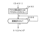
図47は、このように構成された場合の遊技制御手段のマスク不能割込処理(電力供給停止時処理)の一部を示すフローチャートである。図47に示すフローチャートは、図30〜図32に示されたステップS451〜S491の処理に続いて実行される。すなわち、この実施の形態では、RAMアクセスレジスタにアクセス禁止値を設定(ステップS492)した後のシステムリセットを待つ待機状態において、入力ポートを介して復帰信号のオンの検出が実行される(ステップS500)。そして、復帰信号がオンになったら、図17に示されたメイン処理のステップS1にジャンプする。メイン処理の実行が開始されると、電源断信号が出力されたときに遊技状態が保存されているので、ステップS8の処理で遊技状態復旧処理が実行され、遊技制御は、電源断信号発生時の状態に戻り、その状態から遊技制御が続行される。
【0325】
なお、復帰信号は、例えば入力ポート1のビット4(図16参照)に入力される。また、この実施の形態では、復帰信号のオンが検出されると直ちにステップS1にジャンプしたが、ノイズ除去等のために、複数回連続したオンを検出したらステップS1にジャンプするようにしたり、オン検出後所定期間経過後にも再度オンが検出されたらステップS1にジャンプするようにしてもよい。
【0326】
さらに、払出制御手段のマスク不能割込処理においても、入力ポートに入力される復帰信号を検出するようにしてもよい。
【0327】
上記の各実施の形態では、復帰信号は電源基板910で作成されたが、復帰信号を必要とする電気部品制御基板において作成されてもよい。図48は、復帰信号が電気部品制御基板において作成される場合の電源基板910Aの構成例を示すブロック図である。図48に示す電源基板910Aは、図13に示された電源基板910とは異なり、復帰信号を出力しない。
【0328】
リセット管理回路940Aは、図14に示された回路構成から復帰信号生成部分を除いた構成を用いてもよいが、例えば、図49に示すように構成してもよい。図49に示す構成では、リセット管理回路940Aにおいて、それぞれ、VSLを導入して、VSLの電圧値が上昇して所定値以上になると出力をローレベルからハイレベルに変化させるリセットICを有するリセット回路65,65B,65Cが設けられている。リセット回路65の出力は、リセット信号回路950およびバッファ回路965を介して主基板31に対してリセット信号として供給される。なお、各リセットICは、VSLの電圧が低下して所定値を下回ると、出力をハイレベルからローレベルに変化させる。
【0329】
リセット回路65Bの出力は、リセット信号回路950Bおよびバッファ回路961を介して払出制御基板37に対してリセット信号として供給される。なお、リセット信号回路950,950Bの構成は、それぞれ、図14に示されたリセット信号回路950の構成と同じである。そして、リセット回路65Cの出力は、バッファ回路962,963,964を介して、図柄制御基板80、ランプ制御基板35および音声制御基板70に対してリセット信号として供給される。
【0330】
リセット回路65,65B,65Cにおける各リセットICが出力レベルを変化させるための所定値はそれぞれ異なっている。具体的には、リセット回路65のリセットICにおける所定値は、他のリセットICにおける所定値よりも大きい。また、リセット回路65B,65CのリセットICにおける各所定値は、等しいか、または、リセット回路65BのリセットICにおける所定値の方が大きい値である。
【0331】
よって、電源が投入されVSLが上昇していくときには、リセット回路65の出力が最も遅くハイレベルになる。すなわち、主基板31のCPU56が最も遅く立ち上がる。また、電源断時においてVSLが低下していくときには、リセット回路65の出力が最も早くローレベルになる。すなわち、主基板31のCPUが最も早くリセット状態になる。
【0332】
リセット管理回路940Aを図50に示すように構成することもできる。図50に示す構成では、電源が投入されVSLが上昇していくときには、主基板31に対するリセット信号は、AND回路951によって、他の基板へのリセット信号がハイレベルになったことを条件に、ハイレベルになる。従って、主基板31のCPU56が、他の基板におけるCPUよりも遅く立ち上がる。従って、このように構成する場合には、リセット回路65,65B,65Cにおける各リセットICにおける所定値を、図49に示された構成に比べて、さほど厳密に差を付けた値にしなくてもよい。
【0333】
図51は、電源基板910Aにおいて復帰信号が生成されない場合の遊技制御手段のマスク不能割込処理(電力供給停止時処理)の一例を示すフローチャートである。図51に示すフローチャートは、図30〜図32に示されたステップS451〜S491の処理に続いて実行される。すなわち、この実施の形態では、RAMアクセスレジスタにアクセス禁止値を設定(ステップS492)した後のシステムリセットを待つ待機状態において、まず、カウンタの初期値Mが設定される(ステップS111)。そして、カウンタの値を1減算しつつ(ステップS112)、カウンタの値が0になったか否か確認する(ステップS113)。
【0334】
そして、カウンタの値が0になったら、図17に示されたメイン処理のステップS1にジャンプする。メイン処理の実行が開始されると、電源断信号が出力されたときに遊技状態が保存されているので、ステップS8の処理で遊技状態復旧処理が実行され、遊技制御は、電源断信号発生時の状態に戻り、その状態から遊技制御が続行される。
【0335】
カウンタに初期値Mが設定されてからカウントアップ(=0になる)するまでの時間は、[ステップS112およびS113の処理に要する時間]×Mであるが、Mの値は、電源断信号が発生してから、Vcc電源で動作するCPU56が動作不能になるまでに時間よりも長い時間をカウントするように設定される。従って、一般には、一般には、カウンタがカウントアップしてステップS1にジャンプする前に、CPU56は動作しなくなる。すなわち、ステップS1にジャンプすることはない。
【0336】
しかし、電源の瞬断等が生ずると、電源電圧レベルが短期間低下した後に復旧する。その場合にも、VSLの電圧レベルが電源断信号出力レベル以下になると、電源断信号がローレベルになって、電力供給停止時処理が開始される。そして、CPU56は電力供給停止時処理終了後ループ状態に入る。何らの制御も行わないと、ループ処理から抜けられないのであるが、この場合には、カウンタがカウントアップしてメイン処理に復帰することができる。
【0337】
すなわち、この実施の形態におけるカウンタは、電源断信号に応じた処理における待機状態において実行されるタイマ処理を行うためのソフトウェアタイマに相当する。そして、カウンタがカウントアップすると、すなわち、タイマ処理によって所定期間の経過が計測されると、復帰手段としてのCPU56が、待機状態から遊技制御状態に復帰させる制御を行う。
【0338】
このような構成でも、電源の瞬断等に起因して電源断信号が発生したにもかかわらず電源電圧が平常時の値に復旧したときに、CPU56は、図17に示されたメイン処理の実行を再開することができる。その際、電源断信号が出力されたときに遊技状態が保存されているので、ステップS8の処理で遊技状態復旧処理が実行され、遊技制御は、電源断信号発生時の状態に戻り、その状態から遊技制御が続行される。
【0339】
このような制御は、払出制御手段が実行することも可能である。図52は、電源基板910Aにおいて復帰信号が生成されない場合の払出制御手段のマスク不能割込処理(電力供給停止時処理)の一例を示すフローチャートである。図52に示すフローチャートは、図42〜図44に示されたステップS801〜S819の処理に続いて実行される。すなわち、この実施の形態では、RAMアクセスレジスタにアクセス禁止値を設定(ステップS820)した後のシステムリセットを待つ待機状態において、まず、カウンタの初期値Mが設定される(ステップS851)。そして、カウンタの値を1減算しつつ(ステップS852)、カウンタの値が0になったか否か確認する(ステップS853)。
【0340】
そして、カウンタの値が0になったら、図38に示されたメイン処理のステップS701にジャンプする。メイン処理の実行が開始されると、電源断信号が出力されたときに制御状態が保存されているので、ステップS708の処理で払出状態復旧処理が実行され、制御は電源断信号発生時の状態に戻り、その状態から払出制御が続行される。
【0341】
なお、主基板31のCPU56が扱うカウントアップ値(図51におけるS111で設定されるM)は、払出制御用CPU371が扱うカウントアップ値よりも大きい値であることが好ましい。CPU56が扱うカウントアップ値の方が大きい値である場合には、遊技制御手段よりも前に払出制御手段が再起動することになる。従って、払出制御手段が先に立ち上がって、遊技制御手段からの払出制御コマンドを取りこぼすようなことはない。
【0342】
上記のように、電源基板910Aにおいて復帰信号が生成されない場合にソフトウェアによってタイマ処理を行うことによって待機状態から制御状態に戻ることができるが、タイマ処理は、ハードウェアによって実行されてもよい。
【0343】
図53は、電源基板910Aにおいて復帰信号が生成されない場合にハードウェアによってタイマ処理を行うような構成の一例を示すブロック図である。この例では、主基板31に、ウォッチドッグタイマとして機能するカウンタ(ウォッチドッグタイマ回路)162が設けられる。ウォッチドッグタイマ回路162は、発振回路164の出力パルスをカウントし、カウントアップすると、Q出力としてハイレベルの1パルスを発生する。そのパルス信号は、反転回路163で論理反転され、復帰信号としてAND回路161に入力される。AND回路161は、リセット信号と復帰信号の論理積をとってCPU56のリセット端子に供給する。なお、CPU56からシステムクロックまたはその分周クロックを出力するように設定し、そのクロックを、ウォッチドッグタイマ回路162の入力クロック信号としてもよい。
【0344】
カウントアップ値は、電源断信号がローレベルになってから、VSLの電圧値がVcc生成可能電圧にまで低下する時間以上に設定される。ウォッチドッグタイマ回路162はVccを電源として動作するので、カウントアップ値は、ウォッチドッグタイマ回路162の動作可能期間に相当する値以上に設定される。従って、遊技機への電力供給停止時には、一般には、ウォッチドッグタイマ回路162がカウントアップして復帰信号が出力される前に、ウォッチドッグタイマ回路162およびその他の回路部品は動作しなくなる。
【0345】
なお、CPU56が遊技制御を行っているときには、定期的にクリアパルスがウォッチドッグタイマ回路162に与えられる。クリアパルスの出力周期は、ウォッチドッグタイマ回路162がカウントアップするまでの時間よりも短い。従って、CPU56が、通常の遊技制御を行っているときにウォッチドッグタイマ回路162のQ出力にパルスが現れることはない。
【0346】
図54は、ウォッチドッグタイマ回路162が設けられた場合の遊技制御手段のメイン処理の一部を示すフローチャートである。図54に示す処理は、図17に示されたステップS1〜S15の処理に続いて実行される。この場合には、遊技制御処理のループ(ステップS16〜S32)内において、ウォッチドッグタイマクリア処理(ステップS32)が実行される。従って、ウォッチドッグタイマクリア処理は、2ms毎に実行される。
【0347】
ウォッチドッグタイマクリア処理(ステップS32)では、ウォッチドッグタイマ回路162のクリア端子に至る出力ポートに1パルスを出力する処理が行われる。よって、遊技制御処理の実行中では、ウォッチドッグタイマ回路162に定期的にクリアパルスが与えられるので、カウントアップすることはない。
【0348】
遊技機に対する供給電圧が低下して電源断信号が出力されると、図30〜図32に示されたようなマスク不能割込処理が開始される。その処理中ではウォッチドッグタイマ回路162に対してクリアパルスは出力されない。従って、電源電圧が復旧して、ウォッチドッグタイマ回路162がカウントアップするまで動作しているような場合には復帰信号が出力される。
【0349】
図55は、上述したソフトウェアタイマ処理またはウォッチドッグタイマ回路162によって復帰信号が作成される場合の復帰信号の出力タイミング等を示すタイミング図である。図55(A)は、遊技機に対する電力供給が停止された場合の例である。ソフトウェアタイマ処理は電力供給停止時処理が終了して待機状態になってから開始される。また、マスク不能割込処理ではウォッチドッグタイマ回路162に対してクリアパルスは出力されないので、ウォッチドッグタイマ回路16は、実質的に、電力供給停止時処理の開始時から起動される。いずれの場合でも、タイムアップ値(カウントアップ値)は、電源電圧がVcc生成可能電圧値よりも小さくなるまでタイムアップしないように設定されているので、復帰信号が発生することはない。
【0350】
電源の瞬断等が生ずると、図55(B)に示すように、VSLの電圧レベルが短期間低下した後に復旧する。その場合にも、VSLの電圧レベルが電源断信号出力レベル以下になると、電源断信号がローレベルになって、電力供給停止時処理が開始される。そして、CPU56は電力供給停止時処理終了後ループ状態に入る。何らの制御も行わないと、ループ処理から抜けられないのであるが、この場合には、ウォッチドッグタイマ回路16がカウントアップして復帰信号が発生する。
【0351】
図53に示されたように、主基板31において、復帰信号は、AND回路161を介して、CPU56のリセット端子に入力される。従って、CPU56にはシステムリセットがかかる。その結果、CPU56は待機状態から抜け出すことができる。
【0352】
図56は、電源基板910Aにおいて復帰信号が生成されない場合に払出制御基板37におけるハードウェアによってタイマ処理を行うような構成の一例を示すブロック図である。この例では、払出制御基板37に、ウォッチドッグタイマとして機能するカウンタ(ウォッチドッグタイマ回路)386が設けられる。ウォッチドッグタイマ回路386は、発振回路388の出力パルスをカウントし、カウントアップすると、Q出力としてハイレベルの1パルスを発生する。そのパルス信号は、反転回路387で論理反転され、復帰信号としてAND回路385に入力される。AND回路385は、リセット信号と復帰信号の論理積をとってCPU56のリセット端子に供給する。
【0353】
カウントアップ値は、電源断信号がローレベルになってから、VSLの電圧値がVcc生成可能電圧にまで低下する時間以上に設定される。ウォッチドッグタイマ回路386はVccを電源として動作するので、カウントアップ値は、ウォッチドッグタイマ回路386の動作可能期間に相当する値以上に設定される。従って、一般には、ウォッチドッグタイマ回路386がカウントアップして復帰信号が出力される前に、ウォッチドッグタイマ回路386およびその他の回路部品は動作しなくなる。なお、払出制御用CPU371が払出制御を行っているときには、定期的にクリアパルスがウォッチドッグタイマ回路386に与えられる。クリアパルスの出力周期は、ウォッチドッグタイマ回路386がカウントアップするまでの時間よりも短い。従って、払出制御用CPU371が、通常の遊技制御を行っているときにウォッチドッグタイマ回路3876のQ出力にパルスが現れることはない。
【0354】
図57は、ウォッチドッグタイマ回路386が設けられた場合の払出制御手段のメイン処理の一部を示すフローチャートである。図57に示す処理は、図38に示されたステップS701〜S713の処理に続いて実行される。この場合には、払出制御処理のループ(ステップS724〜S760)内において、ウォッチドッグタイマクリア処理(ステップS760)が実行される。従って、ウォッチドッグタイマクリア処理は、2ms毎に実行される。
【0355】
ウォッチドッグタイマクリア処理(ステップS760)では、ウォッチドッグタイマ回路386のクリア端子に至る出力ポートに1パルスを出力する処理が行われる。よって、払出制御処理の実行中では、ウォッチドッグタイマ回路386に定期的にクリアパルスが与えられるので、カウントアップすることはない。
【0356】
遊技機に対する供給電圧が低下して電源断信号が出力されると、図42〜図44に示されたようなマスク不能割込処理が開始される。その処理中ではウォッチドッグタイマ回路386に対してクリアパルスは出力されない。従って、電源電圧が復旧して、ウォッチドッグタイマ回路386がカウントアップするまで動作しているような場合には復帰信号が出力される。
【0357】
図56に示されたように、払出制御基板37において、復帰信号は、AND回路385を介して、払出制御用CPU371のリセット端子に入力される。従って、払出制御用CPU371にはシステムリセットがかかる。その結果、払出制御用CPU371は待機状態から抜け出すことができる。
【0358】
以上のように、主基板31および払出制御基板37においてウォッチドッグタイマ回路162,386が設けられている場合には、ハードウェアによって復帰信号を発生させることができる。しかも、電源電圧が低下したときのみならず、何らかの理由で、CPU56または払出制御用CPU371の制御が無限ループに入ってしまったような場合にも、ループ状態から抜け出すことができる。
【0359】
なお、主基板31のウォッチドッグタイマ回路162のカウントアップ値は、払出制御基板37のウォッチドッグタイマ回路386のカウントアップ値よりも大きい値であることが好ましい。ウォッチドッグタイマ回路162のカウントアップ値の方が大きい値である場合には、復帰信号は、遊技制御手段よりも前に払出制御手段に対して供給される。従って、払出制御手段が先に立ち上がって、遊技制御手段からの払出制御コマンドを取りこぼすようなことはない。
【0360】
また、例えば主基板31のみにウォッチドッグタイマ回路162を設置し、ウォッチドッグタイマ回路162による復帰信号をCPU56に供給するとともに、払出制御基板37に供給してもよい。そのように構成した場合には、全体的な回路構成規模を小さくすることができる。また、そのように構成した場合には、払出制御手段が先に立ち上がるように、ウォッチドッグタイマ回路162とCPU56のリセット端子との間に遅延回路を置くことが好ましい。
【0361】
さらに、ウォッチドッグタイマ回路162,386による復帰信号をCPUのリセット端子に接続するのではなく、入力ポートの入力するようにしてもよい。その場合には、電力供給停止時処理における待機状態で入力ポートの監視が行われ、復帰信号がオンしたことが検出されると、メイン処理の最初にジャンプする。さらに、ウォッチドッグタイマ回路162,386による復帰信号をCPUのCTC端子に入力してもよい。その場合には、あらかじめ、復帰信号の入力に応じてCTC割込がかかるように設定される。また、待機状態で割込許可に設定される。そして、CTC割込がかかると、メイン処理の最初にジャンプする。
【0362】
なお、上記の各実施の形態では、払出制御基板37において、NMIに応じて電力供給停止時処理が実行されたが、電源断信号を払出制御用CPU371のマスク可能端子に接続し、マスク可能割込処理によって電力供給停止時処理を実行してもよい。また、電源断信号を入力ポートに入力し、入力ポートのチェック結果に応じて電力供給停止時処理を実行してもよい。
【0363】
以上説明したように、上記の各実施の形態では、記憶保持手段(例えばバックアップRAM)を有する遊技制御手段および払出制御手段が電源断信号に応じて電力供給停止時処理を行った後にシステムリセットを待つ待機状態にあるときに、電源復旧に応じて復帰信号が出力されると、遊技制御手段および払出制御手段は、プログラムの最初部分から動作を再開する。または、ソフトウェアによるタイマ処理でタイムアウトが生ずると、遊技制御手段および払出制御手段は、プログラムの最初部分から動作を再開する。その際、電力供給停止時処理において保存された制御状態が復旧されるので、遊技者から見ると、何事もなかったかのように遊技が続行される。
【0364】
また、電源基板に設けられている起動順序制御手段が、記憶保持手段を有していない電気部品制御手段と記憶保持手段を有している電気部品制御手段とを含む全ての電気部品制御手段を対象に、リセット信号の供給順序を制御することによって起動順序を制御するので、全ての電気部品制御手段の起動順序制御を、簡単な構成で実現できる。なお、上記の各実施の形態では、記憶保持手段を有していない電気部品制御手段は、表示制御手段、ランプ制御手段および音声制御手段であり、記憶保持手段を有している電気部品制御手段遊技制御手段および払出制御手段である。
【0365】
さらに、起動順序制御手段は、遊技制御手段を最後に起動するので、各電気部品制御手段が、遊技制御手段からの制御コマンドを取りこぼしてしまうという不都合は生じない。
【0366】
また、各種制御データをバックアップRAM領域に保存したあとに、RAMアクセスレジスタにアクセス禁止値を設定して、内蔵RAMのアクセスができなくなるようにしたことで、電源電圧が低下していくときには、各種信号線のレベルが不安定になってRAM内容が化ける可能性があるが、バックアップRAM内のデータが化けることはない。従って、電源電圧が低下していくことに伴って生ずる可能性がある異常動作に起因するRAMの内容破壊等を確実に防止することができる。
【0367】
また、バックアップデータが正常に保持されていなかった場合には、バックアップデータにもとづいて復旧させると不当な制御が実行されてしまうおそれがあるため、そのまま制御状態を復旧させることは好ましくない。上述した各実施の形態では、電力供給開始時に、電力供給停止時にバックアップRAM領域に記憶されたチェックデータ(チェックサムデータ)にもとづいて、初期化処理を行うか遊技状態復旧処理を行うかを決定するように構成したので、停電等の不測の電源断が発生したときに必要なデータを確実に保存することができ、さらに、保存されていたデータを瞬断からの復旧後を含む電源復帰後に確実に活用することができる。
【0368】
なお、上記の各実施の形態では、遊技制御手段および払出制御手段が電源断信号に応じてスイッチ検出処理を行う場合を例示したが、表示制御手段、音制御手段およびランプ制御手段についても、制御状態保存処理が行われる場合に、電源断信号に応じて、所定の電気部品の駆動を停止し、その電気部品に関連するスイッチ手段の検出信号を所定期間に渡って確認した後に、制御状態保存処理を行うように構成してもよい。
【0369】
また、上記の各実施の形態では、復帰信号の入力に応じて、メイン処理(図17、図38)にジャンプするようにしていたが、例えば電源スイッチを備える構成として、復帰信号の入力に応じて、その電源スイッチをオフして、その後ただちにオンするようにしてもよい。
【0370】
また、上記の各実施の形態において、電力供給停止時処理を実行する際に、例えば主基板31であれば表示制御コマンドを送信するなどして、例えば可変表示装置9に「停電処理中です。復帰操作を行って下さい。」の様な表示をするようにしてもよい。このようにすれば、電源の瞬断に起因して待機状態が継続してしまっていても、そのことを報知することができるため、遊技者などが遊技が中断していることを認識することができるようになり、その後の対処をとることが可能となる。
【0371】
また、上記の各実施の形態では、パリティチェックの結果が正当であるときに、初期化処理を実行する構成としていたが、例えば初期化処理を実行することなく、チェック結果に応じた特有の処理を実行するようにしてもよい。この場合、例えば、ROM54の所定の記憶領域に、パリティチェックの結果が不当であるときに実行される制御プログラムを格納しておく。そして、例えばパリティチェックの結果が不当であった場合には、ROM54に記憶されている制御プログラムにもどづく処理が実行され、例えば可変表示装置9に「データが正常に保存されていませんでした」などの表示がされるようにする。また、例えば、初期化処理が実行されたあとに可変表示装置9に表示される特別図柄の初期表示が例えば「1、1、7」である場合に、パリティチェック結果が不当であった場合に可変表示装置9に表示される特別図柄の初期表示を例えば「3、3、7」として、実行された処理が識別可能となるようにする。なお、ランプの点灯パターンや音などによって、実行された処理(あるいは、実行されている処理)が初期化処理であるのか、パリティチェック結果が不当であることに応じた特有の処理であるのかを識別可能とするようにしてもよい。
【0372】
また、上述した各実施の形態では、遊技状態復旧処理においてRAMに記憶されている変動データの全てにもとづいて復旧する構成(ステップS9)としていたが、RAMに記憶されている変動データのうちの一部をクリアして他の一部の変動データにもとづいて復旧するようにしてもよい。この場合、例えば価値付与の数量にかかわる変動データ(例えば、入賞にもとづき払い出される遊技球の数量などを示すデータ)をRAMに記憶されている変動データの一部としてクリアしたり、遊技状態にかかわる変動データ(例えば、大当りか否か、大当り状態、当りか否か、確変か否か、確変状態(確変残り回数など)、時短中か否か、普通図柄や特別図柄の変動時間短縮状態(残り回数)、始動入賞記憶数などを示すデータ)をRAMに記憶されている変動データの一部としてクリアするようにすればよい。すなわち、パリティチェックの結果が正当である場合には、例えば確変フラグや時短フラグをクリアして、クリアされなかった変動データにもとづく遊技状態復旧処理(例えばステップS9)が実行されるようにしてもよい。
【0373】
このように、変動データの一部をクリアすることができる構成とすれば、復旧させることが好ましくないデータ(不当に利益や不利益を与えてしまうおそれのあるデータ)を除く変動データにもとづいて遊技状態を復旧させることができる。なお、変動データの一部として価値付与の数量にかかわる変動データをクリアする構成とすれば、電源断前に得られていた遊技球を、電源投入後に不当に得ることを防止することができる。また、変動データの一部として遊技状態にかかわる変動データをクリアする構成とすれば、電源断前に得られていた例えば確変などの有利な遊技状態を、電源投入後に不当に得ることを防止することができ、あるいは不利な遊技状態を不当に与えてしまうことを防止することができる。
【0374】
また、上記の各実施の形態では、復帰信号を各電気部品制御基板のリセット端子に入力する構成としていたが、例えば電源供給ラインに電源スイッチを設け、復帰信号を電源スイッチに入力する構成としてもよい。この場合、復帰信号が入力すると、電源スイッチは、オフとしたあと直ちにオンとする処理を行うようにすればよい。このように構成すれば、復帰信号の発生に応じて、電源を再投入したときと同じ処理を実行することができ、遊技状態を復帰させることができるようになる。
【0375】
また、上記の各実施の形態では、リセット管理回路940によってリセット信号や復帰信号の出力タイミングなどを一元管理する構成としていたが、例えば各基板によって分散管理するようにしてもよい。この場合、例えば、各基板それぞれに、リセット回路(例えば、図14に示すリセット回路65および各基板に関係する周辺回路と同じ構成の回路)や、復帰信号出力手段(例えば、図14に示す帰信号出力に関する回路のうちの各基板に関係する回路と同じ構成の回路)を設けるように構成すればよい。
【0376】
また、上記の各実施の形態では、電源監視回路は電源基板910に設けられたが、電源監視回路は主基板31や払出制御基板37などの電気部品制御基板に設けられていてもよい。電源回路が搭載された電気部品制御基板が構成される場合には、電源基板には電源監視回路は搭載されない。
【0377】
上記の各実施の形態のパチンコ遊技機1は、主として、始動入賞にもとづいて可変表示部9に可変表示される特別図柄の停止図柄が所定の図柄の組み合わせになると所定の遊技価値が遊技者に付与可能になる第1種パチンコ遊技機であったが、始動入賞にもとづいて開放する電動役物の所定領域への入賞があると所定の遊技価値が遊技者に付与可能になる第2種パチンコ遊技機や、始動入賞にもとづいて可変表示される図柄の停止図柄が所定の図柄の組み合わせになると開放する所定の電動役物への入賞があると所定の権利が発生または継続する第3種パチンコ遊技機であっても、本発明を適用できる。
【0378】
さらに、遊技媒体が遊技球であるパチンコ遊技機に限られず、スロット機等においても、遊技媒体の払い出しを行う電気部品が備えられている場合には本発明を適用することができる。
【0379】
【発明の効果】
以上のように、本発明によれば、遊技機を、遊技制御用マイクロコンピュータおよび払出制御用マイクロコンピュータが、電源監視手段によって遊技媒体検出手段に供給される電圧よりも高い電圧が所定の状態になったことが検出されたことを条件に変動データ記憶手段へのアクセスを禁止する処理を含む電力供給停止時処理を行った後に待機状態に移行し、待機状態中に復帰信号が入力された場合に、記憶内容保持手段により保持された記憶内容にもとづいて制御状態を復帰させる状態復帰制御を実行する構成としたので、復帰信号によって遊技制御用マイクロコンピュータおよび払出制御用マイクロコンピュータを制御実行状態に復帰させることが可能になり、その結果、ごく短時間で復旧する電源の瞬断等にもとづいて待機状態になった場合に自動的に復帰できるという効果を得ることができる。また、電源電圧が低下していくことに伴って生ずる可能性がある異常動作に起因するバックアップ記憶が格納されている領域(例えば、RAM)の内容破壊等を確実に防止することができ、その後の電源投入時に復旧されるRAMの保存データを確実に保護することができる効果がある。電源監視手段が、遊技媒体検出手段に供給される電圧よりも高い電圧を監視するように構成されているので、電源瞬断時の誤検出を防止することができる。
【0385】
払出制御用マイクロコンピュータが、電源監視手段が検出信号を出力したときに、遊技媒体検出手段からの検出信号の入力処理を所定の検出期間実行した後、払出制御用電力供給停止時処理を行うとした場合には、検出すべき遊技媒体を検出することができ、遊技媒体数に関する適正な制御状態をバックアップ記憶することができる。
【0386】
払出制御用マイクロコンピュータが、出力ポートを介して払出手段に駆動信号を出力し、電源監視手段が検出信号を出力したときに、前記払出手段の駆動を停止した後、遊技媒体検出手段からの検出信号の入力処理を実行するとした場合には、払出手段によって新たに遊技媒体が払い出されることがないようにした状態で、遊技媒体の検出を行うことができるため、遊技媒体数に関するさらに適正な制御状態をバックアップ記憶することができる。
【0387】
電源監視手段が検出信号を出力した後の、払出制御用マイクロコンピュータによる遊技媒体検出手段からの検出信号の入力処理の実行中に、払出制御用マイクロコンピュータおよび遊技媒体検出手段を駆動可能な電源を供給可能な補助駆動電源供給手段を備えた場合には、遊技媒体検出手段からの検出信号の入力処理を確実に完了することができるため、適正な遊技媒体の検出処理を行うことが可能となる。
【0388】
遊技媒体検出手段として、賞遊技媒体検出手段と、貸出遊技媒体検出手段とを別個に設けるとした場合には、貸出要求に応じて払い出される遊技媒体の検出と、遊技の進行に応じて払い出される遊技媒体の検出とをそれぞれ別個に行うことが可能となる。
【図面の簡単な説明】
【図1】 パチンコ遊技機を正面からみた正面図である。
【図2】 パチンコ遊技機の裏面に設けられている各基板を示す説明図である。
【図3】 パチンコ遊技機の機構盤を背面からみた背面図である。
【図4】 機構板に設置されている中間ベースユニット周りの構成を示す正面図である。
【図5】 球払出装置を示す分解斜視図である。
【図6】 遊技制御基板(主基板)の回路構成を示すブロック図である。
【図7】 払出制御基板および球払出装置の構成要素などの賞球に関連する構成要素を示すブロック図である。
【図8】 図柄制御基板の回路構成例を示すブロック図である。
【図9】 ランプ制御基板の回路構成例を示すブロック図である。
【図10】 音声制御基板の回路構成例を示すブロック図である。
【図11】 発射制御基板の回路構成例を示すブロック図である。
【図12】 電源基板から各基板に供給される直流電圧等を示すブロック図である。
【図13】 電源基板の一構成例を示すブロック図である。
【図14】 リセット管理回路の構成例を示すブロック図である。
【図15】 タイマ手段の一例であるカウンタの作用を説明するためのタイミング図である。
【図16】 入力ポートのビット割り当ての一例を示す説明図である。
【図17】 主基板におけるCPUが実行するメイン処理の一例を示すフローチャートである。
【図18】 バックアップフラグと遊技状態復旧処理を実行するか否かとの関係の一例を示す説明図である。
【図19】 パリティチェック処理の例を示すフローチャートである。
【図20】 2msタイマ割込処理を示すフローチャートである。
【図21】 RAMにおけるスイッチタイマの形成例を示す説明図である。
【図22】 スイッチ処理の一例を示すフローチャートである。
【図23】 スイッチチェック処理の一例を示すフローチャートである。
【図24】 賞球処理の一例を示すフローチャートである。
【図25】 賞球処理の一例を示すフローチャートである。
【図26】 賞球処理の一例を示すフローチャートである。
【図27】 スイッチオンチェック処理を示すフローチャートである。
【図28】 賞球個数減算処理の一例を示すフローチャートである。
【図29】 入力判定値テーブルの構成例を示す説明図である。
【図30】 遊技制御手段におけるマスク不能割込処理を示すフローチャートである。
【図31】 遊技制御手段におけるマスク不能割込処理を示すフローチャートである。
【図32】 遊技制御手段におけるマスク不能割込処理を示すフローチャートである。
【図33】 バックアップパリティデータ作成方法を説明するための説明図である。
【図34】 検出信号の入力処理が実行される様子の一例を示すタイミング図である。
【図35】 遊技状態復旧処理の一例を示すフローチャートである。
【図36】 出力ポートのビット割り当ての一例を示す説明図である。
【図37】 入力ポートのビット割り当ての一例を示す説明図である。
【図38】 払出制御基板におけるCPUが実行するメイン処理の一例を示すフローチャートである。
【図39】 払出制御手段におけるパリティチェック処理の例を示すフローチャートである。
【図40】 2msタイマ割込処理を示すフローチャートである。
【図41】 払出制御手段におけるRAMの一構成例を示す説明図である。
【図42】 払出制御手段におけるマスク不能割込処理を示すフローチャートである。
【図43】 払出制御手段におけるマスク不能割込処理を示すフローチャートである。
【図44】 払出制御手段におけるマスク不能割込処理を示すフローチャートである。
【図45】 バックアップパリティデータ作成方法を説明するための説明図である。
【図46】 遊技制御基板の他の回路構成を示すブロック図である。
【図47】 遊技制御手段における電力供給停止時処理の他の例を示すフローチャートである。
【図48】 電源基板の他の構成例を示すブロック図である。
【図49】 リセット管理回路の他の構成例を示すブロック図である。
【図50】 リセット管理回路のさらに他の構成例を示すブロック図である。
【図51】 遊技制御手段における電力供給停止時処理の他の例を示すフローチャートである。
【図52】 払出制御手段における電力供給停止時処理の他の例を示すフローチャートである。
【図53】 遊技制御手段の他の構成例の一部を示すブロック図である。
【図54】 主基板におけるCPUが実行するメイン処理の他の例を示すフローチャートである。
【図55】 ソフトウェアタイマおよびウォッチドッグタイマ回路の作用を説明するためのタイミング図である。
【図56】 払出制御手段の他の構成例の一部を示すブロック図である。
【図57】 払出制御基板におけるCPUが実行するメイン処理の他の例を示すフローチャートである。
【符号の説明】
31 遊技制御基板(主基板)
37 払出制御基板
54 ROM
55 RAM
56 CPU
57 I/Oポート
162 ウォッチドッグタイマ回路
371 払出制御用CPU
385 ウォッチドッグタイマ回路
910,910A 電源基板
940,940A リセット管理回路
971 カウンタ(タイマ手段)[0001]
BACKGROUND OF THE INVENTION
The present invention relates to a gaming machine such as a pachinko gaming machine, a coin gaming machine, or a slot machine in which a game is played in accordance with a player's operation.
[0002]
[Prior art]
As an example of a gaming machine, a game medium such as a game ball is launched into a game area by a launching device, and when a game medium is won in a prize area such as a prize opening provided in the game area, a predetermined number of prize balls are awarded to the player There are things that will be paid out. Further, a variable display unit capable of changing the display state is provided, and is configured to give a predetermined game value to the player when the display result of the variable display unit becomes a predetermined specific display mode There is.
[0003]
The game value means that the state of the variable winning ball device provided in the gaming area of the gaming machine is advantageous to a player who is easy to win and a right to become advantageous to the player. Or a condition that the conditions for paying out premium game media are easily established.
[0004]
In the first type pachinko gaming machine having a variable display unit that displays a special symbol, the display result of the variable display unit that displays the special symbol is usually a combination of a specific display mode defined in advance. " When a big hit occurs, for example, the big winning opening is opened a predetermined number of times, and the game shifts to a big hit gaming state in which a hit ball is easy to win. And in each open period, if there is a prize for a predetermined number (for example, 10) of the big prize opening, the big prize opening is closed. And the number of times the special winning opening is opened is fixed to a predetermined number (for example, 16 rounds). Note that an opening time (for example, 29.5 seconds) is determined for each opening, and even if the number of winnings does not reach a predetermined number, the big winning opening is closed when the opening time elapses. Further, when a predetermined condition (for example, winning in the V zone provided in the big prize opening) is not established at the time when the big prize opening is closed, the big hit gaming state is ended.
[0005]
In addition, among the combinations of display modes other than the “big hit” combination, the display results that are already deterministic or temporary at the stage where some of the display results of the plurality of variable display portions are not yet derived and displayed. A state in which the display mode of the variable display unit in which “” is derived and displayed satisfies a display condition that is a combination of specific display modes is referred to as “reach”. Then, when the display result of the identification information variably displayed on the variable display section does not satisfy the condition of “big hit”, it becomes “disconnected”, and the variable display state ends. A player plays a game while enjoying how to generate a big hit.
[0006]
When a game ball wins a winning opening provided on the game board, a predetermined number of prize balls are paid out. Since the progress of the game is controlled by game control means mounted on the main board, the number of winning balls based on the winning is determined by the game control means and transmitted to the payout control board. In the following description, the game control means and other control means control various electrical components provided in the gaming machine, so they may be referred to as electrical component control means.
[0007]
[Problems to be solved by the invention]
As described above, various electrical component control means including game control means are mounted in the gaming machine. In general, each electrical component control means includes a microcomputer. Such an electrical component control means generally performs an initialization process and starts control from an initial state when a power supply voltage rises. Then, an unexpected power interruption such as a power failure occurs, and thereafter, when the power is restored, the state returns to the initial state, which may cause a problem such as loss of the game value obtained by the player. In order to prevent such a problem from occurring, the game control is interrupted according to a predetermined signal generated as the power supply voltage value decreases, and the power supply to the gaming machine is stopped at that time. In particular, it may be controlled to store in a storage means (backup storage means) that is backed up and wait for the power supply to be completely stopped. Such a gaming machine resumes the game based on the stored control state when power supply is resumed while the game state is stored in the storage means, so that a disadvantage is given to the player. Is prevented.
[0008]
However, when the power supply voltage is lowered for a very short period due to a momentary power interruption or the like, the power supply voltage is recovered immediately. In such a case, it is conceivable that the control of the microcomputer does not completely escape from the state of waiting for the power supply to be completely stopped. That is, it is possible that the gaming machine control does not return to the normal state even though the power supply to the gaming machine is in the normal state.
[0009]
Further, when the power supply is in a state of waiting for complete stoppage, the power supply is in an unstable state, so that the storage contents of the backup storage may be destroyed.
[0010]
Therefore, in the gaming machine configured to save the control state at that time when the power supply is unexpectedly interrupted, the control is hindered even if a power supply interruption that recovers in a very short time occurs. It is an object of the present invention to provide a gaming machine that can prevent the occurrence of a failure and can guarantee the safety of the contents of a backup storage even in a situation where power supply is unstable.
[0011]
[Means for Solving the Problems]
A gaming machine according to the present invention is a gaming machine in which a player can play a predetermined game using a game medium, and is generated when a game medium detection means for detecting the game medium and control is performed. There is a game control variation data storage means for storing variation data, and there is a game control microcomputer for controlling the progress of the game, and a payout control variation data storage means for storing the variation data generated during the control. AndOperate payout means for paying out game mediaA payout control microcomputer for controlling the payout of game media, and the contents stored in the game control variation data storage means and the payout control variation data storage means for a predetermined period even when power supply to the game machine is stopped Game content control means, and a power supply monitoring means for monitoring the voltage higher than the voltage supplied to the game medium detection means and outputting a detection signal when the occurrence of power interruption is detected. The microcomputer for the computer responds to the input of the detection signal.Processing for setting a backup flag in the variation data storage means for game control, creation processing of check data used for determining whether or not the stored contents of the variation data storage means for game control are normal, andAfter performing the game control power supply stop process including the process of prohibiting access to the game control variation data storage means, the process shifts to a standby state, and the payout control microcomputer responds to the input of the detection signal.A process of stopping the operation of the payout means, a process of setting a backup flag in the payout control variable data storage means, a check data creation process used to determine whether or not the storage content of the payout control variable data storage means is normal, andAfter performing processing at the time of stoppage of power supply for payout control including processing for prohibiting access to the variable data storage means for payout control, transition to a standby state,In the process of stopping power supply for payout control, the process for stopping the operation of the payout means precedes the process for setting a backup flag, the process for creating check data, and the process for prohibiting access to the variable data storage means for payout control. Run,The game control microcomputer includes a return signal output means for outputting a return signal for returning from the standby state when the power supply is not stopped after a predetermined period after the power supply monitoring means outputs the detection signal. ,When power supply is started orWhen a return signal is input during standby,On condition that the backup flag is set in the game control variation data storage means and that the storage content of the game control variation data storage means is confirmed to be normal based on the check data,Based on the stored contents of the game control variation data storage means, execute the game control state return control to return the control state to the state when the game control power supply stop processing was started,If the backup flag is not set in the game control variable data storage means, the memory contents of the game control variable data storage means are initialized regardless of whether the game control variable data storage means is normal or not. Execute the process toThe dispensing control microcomputerWhen power supply is started orWhen a return signal is input during standby,On the condition that the backup flag is set in the payout control variable data storage means and that the storage contents of the payout control variable data storage means are confirmed to be normal based on the check data,Based on the storage contents of the fluctuation data storage means for payout control, execute the return control state for payout control to return the control state to the state when the power supply for payout control was stoppedIf the backup flag is not set in the payout control variable data storage means, the storage contents of the payout control variable data storage means are stored regardless of whether the storage contents of the payout control variable data storage means are normal. Execute the initialization processIt is characterized by that.
[0013]
The return signal output means includes a first return signal output means for outputting a return signal to the game control microcomputer, and a second return signal output means for outputting the return signal to the payout control microcomputer. After the return signal output means outputs a return signal to the payout control microcomputer, the first return signal output means returns to the game control microcomputer.It may be configured to output a signal.
[0014]
PlayThe technical medium detection means detects the game medium paid out from the payout means, and the payout control microcomputer performs input processing of the detection signal from the game medium detection means when the power supply monitoring means outputs the detection signal. After executing the predetermined detection period, it may be configured to perform processing at the time of stopping power supply for payout control.
[0015]
The payout control microcomputer outputs a drive signal to the payout means via the output port, and when the power supply monitoring means outputs a detection signal, after the drive of the payout means is stopped, the detection signal from the game medium detection means Execute input processingYou may be comprised so that.
[0016]
A power supply capable of driving the payout control microcomputer and the game medium detection means during execution of the detection signal input process from the game medium detection means by the payout control microcomputer after the power supply monitoring means outputs the detection signal. Auxiliary drive power supply means that can be supplied is providedIt is preferable.
[0017]
As game medium detection means, a prize game medium detection means for detecting a game medium paid out from a payout means in response to a winning, and a rental game medium detection for detecting a game medium paid out from the payout means in response to a loan request Means separatelyMay be.
[0018]
The payout control microcomputer is set so that a timer interrupt is periodically generated when the power supply is started, and the game medium is paid out based on the occurrence of the regularly generated timer interrupt. Execute interrupt processing for control,Based on the establishment of the interrupt prohibition condition, set the interrupt prohibition state to prohibit the execution of interrupt processing,In the process of stopping power supply for payout control,PercentWhen the power supply is started by executing the process that saves the interrupt status data indicating the interrupt disabled status or the interrupt enabled status that permits execution in the variable data storage means It may be configured to perform a state recovery process for recovering to an interrupt prohibited state or an interrupt permitted state based on the state data.
[0019]
The game control microcomputer transmits a payout control command for designating the number of payouts of the game medium according to the winning to the payout control microcomputer, and the payout control microcomputer receives the payout control command in response to the payout control command. When the payout control command is received, control is set to an interrupt disabled state.It may be configured to.
[0020]
The game control microcomputer is set so that a timer interrupt is periodically generated when power supply is started, and the progress of the game is controlled based on the occurrence of the regularly generated timer interrupt. Execute interrupt processing toBased on the establishment of the interrupt prohibition condition, set the interrupt prohibition state to prohibit the execution of interrupt processing,In the process of stopping power supply for game control,PercentWhen power supply is started by executing a process for storing interrupt state data in the game prohibition state or interrupt permission state permitting execution in the game control variable data storage means. The state recovery process for recovering to the interrupt prohibited state or the interrupt permitted state based on the interrupt state data may be performed.
[0021]
DETAILED DESCRIPTION OF THE INVENTION
Hereinafter, an embodiment of the present invention will be described with reference to the drawings.
First, an overall configuration of a pachinko gaming machine that is an example of a gaming machine will be described. FIG. 1 is a front view of the
[0022]
As shown in FIG. 1, the
[0023]
Near the center of the
[0024]
An open /
[0025]
The
[0026]
In this example, a prize ball lamp 51 that is lit when there is a remaining number of prize balls is provided in the vicinity of one
[0027]
The
[0028]
The hit ball fired from the hit ball launching device enters the
[0029]
The rotation of the image in the
[0030]
When the combination of images in the
[0031]
Next, each board | substrate arrange | positioned at the back surface of the
As shown in FIG. 2, on the back surface of the
[0032]
On the back side of the gaming machine, there are installed a variable
[0033]
Furthermore, a
[0034]
FIG. 3 is a rear view of the mechanism plate of the
[0035]
The game balls paid out from the
[0036]
A lot of premium balls based on the winnings are paid out and the hitting
[0037]
Next, the configuration of the intermediate base unit installed on the
[0038]
A
[0039]
The ball break switches 187a and 187b are locked by locking pieces 188 at positions where it can be detected that about 27 to 28 game balls are present in the
[0040]
The central portion of the
[0041]
Below the
[0042]
FIG. 5 is an exploded perspective view of the
[0043]
As shown in FIG. 5, the
[0044]
The
[0045]
In addition, below the ball
[0046]
[0047]
A recess is formed at the tip of the
[0048]
In other words, the payout motor position sensor including the
[0049]
When the
[0050]
As shown in FIG. 4, a
[0051]
In this way, by providing the
[0052]
In this embodiment, a
[0053]
FIG. 6 is a block diagram illustrating an example of a circuit configuration in the
[0054]
Although not shown in FIG. 6, the count switch short-circuit signal is also transmitted to the basic circuit 53 via the switch circuit 58.
[0055]
Further, according to the data given from the basic circuit 53, the jackpot information indicating the occurrence of the jackpot, the effective starting information indicating the number of starting winning balls used for starting the image display of the
[0056]
The basic circuit 53 includes a ROM 54 that stores a game control program and the like, a
[0057]
A ball hitting device for hitting and launching a game ball is driven by a
[0058]
In this embodiment, a reset signal whose low level indicates a reset state, a low active return signal, and a low active power-off signal are also input from the
[0059]
In this embodiment, the lamp control means mounted on the
[0060]
FIG. 7 is a block diagram showing components related to payout, such as components of the
[0061]
The CPU 56 of the
[0062]
Further, the detection signal from the prize
[0063]
When there is a winning, a payout control command indicating the number of winning balls is input to the
[0064]
In the
[0065]
The
[0066]
Further, a detection signal from the ball lending
[0067]
The
[0068]
A ball lending switch signal and a return switch signal are given from the
[0069]
When the power of the
[0070]
Then, the
[0071]
As described above, all signals from the
[0072]
In this embodiment, a reset signal, a return signal, and a power-off signal are also input from the
[0073]
In this embodiment, the case where the
[0074]
FIG. 8 shows the circuit configuration in the
[0075]
As shown in FIG. 8, a reset signal is supplied from the
[0076]
The display control CPU 101 operates in accordance with a program stored in the control data ROM 102. When an INT signal is input from the
[0077]
Then, the display control CPU 101 performs display control of the screen displayed on the
[0078]
8 also shows a
[0079]
The input buffer circuits 105A and 105B can pass signals only in the direction from the
[0080]
The outputs of the
[0081]
In addition, for example, a three-terminal capacitor or a ferrite bead is used as the
[0082]
FIG. 9 is a block diagram showing signal transmission / reception portions in the
[0083]
A reset signal is supplied from the
[0084]
As shown in FIG. 9, the lamp control command related to the lamp control is output from the output ports (
[0085]
In the
[0086]
In the
[0087]
Further, the lamp control CPU 351 outputs a light on / off signal to the
[0088]
As the
[0089]
In the
[0090]
FIG. 10 is a block diagram showing a configuration example of the voice control command signal transmission portion of the
[0091]
The
[0092]
As shown in FIG. 10, the voice control command is output from the output ports (
[0093]
Then, for example, a
[0094]
As the
[0095]
In the
[0096]
FIG. 11 is a block diagram showing a
[0097]
The
[0098]
The touch sensor circuit 93 outputs a firing permission signal to the
[0099]
FIG. 12 is a block diagram showing DC voltage and the like supplied from the
[0100]
In this embodiment, the
[0101]
As shown in FIG. 12, the ground side of the voltage supplied to each substrate is shared by the
[0102]
FIG. 13 is a block diagram illustrating a configuration example of the
[0103]
The transformer 911 converts AC voltage from the AC power source into 24V. The AC 24V voltage is output to the
[0104]
However, each connector reaching each electric component control board may be provided on the
[0105]
The + 5V line from the DC-
[0106]
A battery that can be charged from a + 5V power supply may be used as the backup power supply. In the case of using a battery, a rechargeable battery is used in which the capacity disappears when a state in which no power is supplied from the +5 V power source continues for a predetermined time.
[0107]
Further, a power
[0108]
The predetermined value for the
[0109]
Furthermore, when VSL (+ 30V) is used as the monitoring voltage, the voltage supplied to the various switches of the gaming machine is + 12V, so that it can be expected to prevent erroneous switch-on detection at the time of instantaneous power interruption. That is, when the voltage of the + 30V power supply is monitored, it is possible to detect a decrease in the level before + 12V created after the creation of + 30V starts to drop. Therefore, when the voltage of the + 12V power supply decreases, the switch output becomes an on-state. However, if the power-off is recognized by monitoring the + 30V power supply voltage that decreases faster than + 12V, the switch output is turned on before the switch output shows the on-state. It is possible to enter a state of waiting for recovery and not detect switch output.
[0110]
Further, since the
[0111]
In the configuration shown in FIG. 13, the detection output (power cut-off signal) of the
[0112]
Further, a
[0113]
FIG. 14 is a block diagram illustrating a configuration example of the
[0114]
The reset IC 651 monitors the power supply voltage of VSL, which is the power supply voltage equal to the power supply voltage monitored by the power
[0115]
As shown in FIG. 14, the reset signal from the reset IC 651 is input to the
[0116]
The Q6 output of the counter IC 941 is input to the clock terminal of the flip-flop (FF) 942. The D input of the flip-
[0117]
For example, the detection voltage of the
[0118]
In this example, the detection condition for the power supply monitoring means to output a detection signal is that the + 30V power supply voltage has dropped to + 22V, and the condition for the reset IC 651 to output a low level that is a reset level is + 30V. The power supply voltage has dropped to + 9V. However, the voltage value used here is an example, and other values may be used.
[0119]
However, although the monitoring range is narrowed, it is also possible to use a + 5V power supply voltage as the monitoring voltage of the power supply monitoring means and the reset IC 651. Even in that case, the detection voltage of the power monitoring circuit is set higher than the detection voltage of the reset IC 651.
[0120]
While power is not supplied from the + 5V power supply that is the driving power source of the CPU 56 and the
[0121]
FIG. 14 shows a configuration in which the reset signal (low level signal) is given twice to the reset terminal of the CPU of each electrical component control board when the power is turned on, but the rising timing of the reset signal is only once. When using a CPU that reliably releases reset even if not, the circuit elements denoted by reference numerals 941 to 949 are not necessary. In that case, the output of the reset IC 651 is directly connected to the buffer circuits 961 to 964 and the
[0122]
In this embodiment, when a reset signal is supplied from the
[0123]
For example, when the CPU 56 of the
[0124]
Further, a counter 971 which is an example of timer means is mounted on the
[0125]
The output of the buffer circuit 973 becomes a return signal to the
[0126]
FIG. 15 is a timing chart for explaining the operation of the counter 971. As shown in FIG. 15A, when the power supply voltage decreases and the voltage value of VSL decreases to the power-off signal output level (+22 V in this example), a power-off signal is generated. Specifically, the power-off signal becomes low level. Then, as will be described later, the
[0127]
The counter 971 starts counting when the power-off signal becomes low level, but the count-up value is the time for the voltage value of VSL to drop to a voltage capable of generating Vcc after the power-off signal becomes low level. Set as above. That is, at least the power supply voltage is set to be equal to or longer than the time during which the power supply voltage is reduced to a voltage at which the control operation is disabled. Since the counter 971 operates using Vcc as a power source, the count-up value is set to be equal to or greater than the value corresponding to the operable period of the counter 971. Therefore, generally, the counter 971 and other circuit components do not operate before the counter 971 counts up and a return signal is output.
[0128]
When an instantaneous power interruption or the like occurs, as shown in FIG. 15B, the voltage level of VSL is restored after a short period of time drop. When the voltage level of VSL becomes equal to or lower than the power-off signal output level, the power-off signal becomes low level, and the power supply stop process is started. Then, the CPU 56 and the
[0129]
As shown in FIGS. 6 and 7, in the
[0130]
FIG. 15B shows a case where a return signal is output immediately after the counter 971 counts up, but the
[0131]
FIG. 16 is an explanatory diagram showing bit assignment of input ports in this embodiment. As shown in FIG. 16, the winning
[0132]
Next, the operation of the gaming machine will be described.
FIG. 17 is a flowchart showing a main process executed by the CPU 56 on the
[0133]
In the initial setting process, the CPU 56 first sets the interrupt prohibition (step S1). Next, the interrupt mode is set to interrupt mode 2 (step S2), and a stack pointer designation address is set to the stack pointer (step S3). Then, the built-in device register is initialized (step S4). Further, after initialization (step S5) of CTC (counter / timer) and PIO (parallel input / output port) which are built-in devices (built-in peripheral circuits), the RAM is set to an accessible state (step S6).
[0134]
The CPU 56 used in this embodiment has the following three types of maskable interrupt (INT) modes. When a maskable interrupt occurs, the CPU 56 automatically sets the interrupt disabled state and saves the contents of the program counter in the stack.
[0135]
Interrupt mode 0: The built-in device that has issued the interrupt request sends an RST instruction (1 byte) or a CALL instruction (3 bytes) onto the internal data bus of the CPU. Therefore, the CPU 56 executes the instruction at the address corresponding to the RST instruction or the address specified by the CALL instruction. At reset, the CPU 56 automatically enters interrupt
[0136]
Interrupt mode 1: In this mode, when an interrupt is accepted, the mode always jumps to address 0038 (h).
[0137]
Interrupt mode 2: A mode in which the address synthesized from the value (1 byte) of the specific register (I register) of the CPU 56 and the interrupt vector (1 byte: least significant bit 0) output by the built-in device indicates the interrupt address It is. That is, the interrupt address is an address indicated by 2 bytes in which the upper address is the value of the specific register and the lower address is the interrupt vector. Therefore, an interrupt process can be set at an arbitrary address (although it is skipped). Each built-in device has a function of sending an interrupt vector when making an interrupt request.
[0138]
Therefore, when the interrupt
[0139]
Next, the CPU 56 checks whether or not data protection processing for the backup RAM area (for example, power failure occurrence NMI processing such as addition of parity data) has been performed when the power is turned off (step S7). In this embodiment, when an unexpected power failure occurs, processing for protecting data in the backup RAM area is performed. When such protection processing is performed, it is assumed that there is a backup. When it is confirmed that there is no backup, the CPU 56 executes an initialization process.
[0140]
In this embodiment, whether or not there is backup data in the backup RAM area is confirmed by the state of the backup flag set in the backup RAM area when the power is turned off. In this example, as shown in FIG. 18, if “55H” is set in the backup flag area, it means that there is a backup (ON state), and if a value other than “55H” is set, there is no backup (OFF). State).
[0141]
After confirming that there is a backup, the CPU 56 performs a data check of the backup RAM area (parity check in this example).
[0142]
FIG. 19 is a flowchart illustrating an example of the parity check process in step S8. In the parity check process, the CPU 56 first checks whether the data set in the backup parity data area in the
[0143]
In the case of recovery after an unexpected power failure, the data in the backup RAM area should have been saved, so the check result is normal. If the check result is not normal, the internal state cannot be returned to the state at the time of power-off, and therefore an initialization process that is executed at the time of power-on not at the time of power failure recovery is executed.
[0144]
If the check result is normal (step S8), the CPU 56 performs a game state restoration process for returning the internal state of the game control means and the control state of the electric component control means such as the display control means to the state when the power is cut off. (Step S9). Then, the saved value of the PC (program counter) saved in the backup RAM area is set in the PC, and the address is restored.
[0145]
In this embodiment, after the presence or absence of backup data is confirmed in step S7, the backup area is checked in step S8 when backup data exists. Conversely, the backup area check result is After it is confirmed that the data is normal, the presence / absence of backup data may be confirmed. Further, it may be determined whether or not to execute the power failure recovery processing by confirming either one of the presence / absence of backup data or the check of the backup area.
[0146]
Further, for example, in the parity check (step S8) when determining whether or not to execute the power failure recovery processing, that is, when determining whether or not to restore the gaming state, a special process in the stored RAM data If it is confirmed that the gaming machine is in a game standby state (not changing in design, not in big hit game, not in probable change, or without starting winning memory) by flag or the starting winning memory data The initialization process may be executed without performing the game state restoration process.
[0147]
As described above, in this embodiment, when power supply is started, initialization processing or game state restoration processing is performed based on the check data (checksum data) stored in the backup RAM area when power supply is stopped. Because it is configured to determine whether or not an unexpected power failure such as a power failure occurs, the necessary data can be saved reliably, and the saved data must be used reliably after the power is restored. Can do.
[0148]
In the above-described embodiment, the normal initialization process is executed when the checksum confirmation result is not valid. However, the checksum confirmation result is not valid. Also, the initialization process may not be performed.
[0149]
For example, if the result of the checksum confirmation is not valid, the game state recovery process may be performed after the stored contents of the backup RAM are restored without executing the initialization process. In this case, for example, an error correction code (for example, a Hamming code used for countermeasures against random errors or a Fire code used for countermeasures against burst errors may be selected according to error characteristics) for data restoration. Thus, the changed bits may be detected and corrected.
[0150]
Further, for example, when the result of the checksum confirmation is not valid, it may be notified that an abnormality has occurred in the stored contents of the backup RAM without executing the initialization process. In this case, the abnormality notification is performed by, for example, displaying the occurrence of an abnormality on the
[0151]
In the initialization process, the CPU 56 first performs a RAM clear process (step S11). Also, initial value setting processing is performed for setting initial values in predetermined work areas (for example, a normal symbol determination random number counter, a normal symbol determination buffer, a special symbol left middle right symbol buffer, a payout command storage pointer, etc.). Further, processing for initializing the sub-boards (
[0152]
Then, a CTC register set in the CPU 56 is set so that a timer interrupt is periodically generated every 2 ms (step S14). That is, a value corresponding to 2 ms is set in a predetermined register (time constant register) as an initial value. Since the interruption is prohibited in step S1 of the initial setting process, the interruption is permitted before the initialization process is completed (step S15).
[0153]
In this embodiment, the built-in CTC of the CPU 56 is set to repeatedly generate a timer interrupt. In this embodiment, the repetition period is set to 2 ms. When a timer interrupt occurs, as shown in FIG. 20, the CPU 56 sets a timer interrupt flag indicating that a timer interrupt has occurred, for example (step S12).
[0154]
When the execution of the initialization process (steps S11 to S15) is completed, the main process shifts to a loop process in which it is confirmed whether or not a timer interrupt has occurred (step S17). In the loop, display random number update processing (step S16) is also executed.
[0155]
When the CPU 56 recognizes that a timer interrupt has occurred in step S17, it executes the game control process of steps S21 to S31. In the game control process, the CPU 56 first inputs the states of the switches such as the
[0156]
Next, various abnormality diagnosis processes are performed by the self-diagnosis function provided in the
[0157]
Next, a process of updating each counter indicating each determination random number such as a big hit determination random number used for game control is performed (step S23). The CPU 56 further performs a process of updating a display random number such as a random number that determines the type of stop symbol (step S24).
[0158]
Further, the CPU 56 performs special symbol process processing (step S25). In the special symbol process control, corresponding processing is selected and executed according to a special symbol process flag for controlling the
[0159]
Next, the CPU 56 performs a process of setting a display control command related to the special symbol in a predetermined area of the
[0160]
Further, the CPU 56 performs information output processing for outputting data such as jackpot information, start information, probability variation information supplied to the hall management computer, for example (step S29).
[0161]
Further, the CPU 56 issues a drive command to the solenoid circuit 59 when a predetermined condition is established (step S30). The solenoid circuit 59 drives the
[0162]
Then, the CPU 56 executes a prize ball process for setting the number of prize balls based on the detection outputs of the
[0163]
With the above control, in this embodiment, the game control process is started every 2 ms. In this embodiment, in the timer interrupt process, for example, only a flag indicating that an interrupt has occurred is set, and the game control process is executed in the main process, but the game control process is performed in the timer interrupt process. May be executed.
[0164]
In addition, the main process includes a process for determining whether or not to shift to the game control process, and whether or not the CPU 56 should shift to the game control process by the timer interrupt process based on the timer interrupt generated periodically. Since the flag for determining whether or not is set, etc., all of the game control processing is reliably executed. In other words, until all the game control processes are executed, it is not determined whether or not to shift to the next game control process, so it is guaranteed that all the processes in the game control process are completed. ing.
[0165]
As described above, in this embodiment, the interrupt
[0166]
Note that after the setting of CTC and PIO (step S5) is completed, an internal register for determining the frequency of the clock signal output from the IEO / SCLK0 terminal may be set. At that time, the frequency of the clock signal is set to a frequency corresponding to 2 ms which is the start cycle of the game control process. When such setting is performed, a clock signal having a frequency corresponding to the activation period of the game control process is externally output from the CPU 56 from the IEO / SCLK0 terminal. Then, a signal corresponding to the activation cycle of the game control process can be observed outside the CPU 56. Therefore, it becomes easy to simulate a game control process by the CPU 56 and to test an operation state of the CPU 56 outside the gaming machine using such a signal.
[0167]
Next, a specific example of the switch process (step S21) in the main process will be described. In this embodiment, when the ON state of the detection signal continues for a predetermined time, it is certainly determined that the switch is turned on, and processing corresponding to the switch on is started. A switch timer is used to measure the predetermined time. The switch timer is a 1-byte counter formed in the backup RAM area, and is incremented by 1 every 2 ms when the detection signal indicates an ON state. As shown in FIG. 21, the switch timer is provided by the number N of detection signals. In this embodiment, N = 12. In the RAM, the addresses of the switch timers are arranged in the same order as the bit arrangement order of the input ports (from top to bottom shown in FIG. 16).
[0168]
FIG. 22 is a flowchart illustrating a processing example of the switch processing in step S21 in the game control processing. The switch process is first executed in the game control process as shown in FIG. In the switch process, the CPU 56 first inputs data input to the input port 0 (step S71). Next, “8” is set as the number of processes (step S72), and the address of the switch timer for the winning
[0169]
FIG. 23 is a flowchart showing a switch check processing subroutine. In the switch check processing subroutine, the CPU 56 sets port input data, in this case, input data from the
[0170]
If the value of the carry flag is “1” (step S85), that is, if the detection signal of the winning
[0171]
If the value of the carry flag is “0”, that is, if the detection signal of the winning
[0172]
Thereafter, the CPU 56 adds 1 to the pointer (switch timer address) (step S90) and subtracts 1 from the number of processes (step S91). If the number of processes is not 0, the process returns to step S82. Then, the processes in steps S82 to S92 are repeated.
[0173]
The processes of steps S82 to S92 are repeated for the number of processes, that is, eight times, and during that time, the detection signal of the switch input to the 8 bits of the
[0174]
The CPU 56 inputs the data input to the
[0175]
In the switch check processing subroutine, since the above-described processing is executed, the processing of steps S82 to S92 is repeated for the number of processing, that is, four times, and the detection signal of the switch input to the 4 bits of the
[0176]
In this embodiment, since the game control process is started every 2 ms, the switch process is also executed once every 2 ms. Therefore, the switch timer is incremented by 1 every 2 ms.
[0177]
FIGS. 24-26 is a flowchart which shows an example of the prize ball process of step S31 in a game control process. In this embodiment, in the prize ball processing, it is determined whether or not the
[0178]
In the prize ball process, the CPU 56 sets “0” as the offset of the input determination value table (step S121), and sets “0” as the offset of the address of the switch timer (step S122). The offset “0” in the input determination value table means that the first data in the input determination value table is used. Also, since the switch timers are arranged in the same order as the bit order of the input ports shown in FIG. 16, the switch timer address offset “0” designates the switch timer corresponding to the winning
[0179]
The input determination value table is a ROM area in which a determination value for determining that the switch has been turned on when it is detected how many times it is continuously turned on is set for each switch. A configuration example of the input determination value table is shown in FIG. As shown in FIG. 29, the input determination value table includes “2”, “50”, “250”, “30”, “250”, “1” in order from the top, that is, in order from the smallest address value. The judgment value is set. In the switch-on check routine, the judgment value set at the address determined by the head address and the offset value in the input judgment value table is compared with the value of the switch timer determined by the head address and the offset value of the switch timer. If they match, for example, a switch-on flag is set.
[0180]
An example of the switch-on check routine is shown in FIG. In the switch-on check routine, the CPU 56 sets the head address of the input determination value table (see FIG. 29) (step S101). Then, an offset is added to the address (step S102), and a switch-on determination value is loaded from the address after the addition (step S103).
[0181]
Next, the CPU 56 sets the start address of the switch timer (step S104), adds an offset to the address (step S105), and loads the value of the switch timer from the address after the addition (step S106). Since each switch timer is arranged in the same order as the bit order of the input ports shown in FIG. 16, the value of the switch timer corresponding to the switch is loaded.
[0182]
Then, the CPU 56 compares the loaded switch timer value with the switch-on determination value (step S107). If they match, a switch-on flag is set (step S108).
[0183]
In this case, in the switch-on check routine, the switch-on flag is set if the value of the switch timer corresponding to the winning
[0184]
Next, the CPU 56 sets “0” as the offset of the input determination value table (step S130), and sets “4” as the offset of the switch timer address (step S131). The offset “0” in the input determination value table means that the first data in the input determination value table is used. Also, since the switch timers are arranged in the same order as the bit order of the input ports shown in FIG. 16, the switch timer address offset “4” designates the switch timer corresponding to the
[0185]
In the switch-on check routine, if the value of the switch timer corresponding to the
[0186]
Next, the CPU 56 sets “0” as the offset of the input determination value table (step S135), and sets “5” as the offset of the switch timer address (step S136). The offset “0” in the input determination value table means that the first data in the input determination value table is used. Further, since the switch timers are arranged in the same order as the bit order of the input ports shown in FIG. 16, the switch timer address offset “5” indicates that the switch timer corresponding to the
[0187]
In the switch-on check routine, if the value of the switch timer corresponding to the
[0188]
Further, the CPU 56 sets “1” as the offset of the input determination value table (step S150), and sets “9” as the offset of the switch timer address (step S151). The offset “1” in the input determination value table means that the second data “50” in the input determination value table is used. Further, since the switch timers are arranged in the same order as the bit order of the input ports shown in FIG. 16, the switch timer address offset “9” designates the switch timer corresponding to the
[0189]
In the switch-on check routine, if the value of the switch timer corresponding to the
[0190]
Further, the CPU 56 sets “2” as the offset of the input determination value table (step S156), and sets “0A (H)” as the offset of the switch timer address (step S157). The offset “2” in the input determination value table means that the third data “250” in the input determination value table is used. Further, since the switch timers are arranged in the same order as the bit order of the input ports shown in FIG. 16, the switch timer address offset “0A (H)” is designated by the switch timer corresponding to the ball break
[0191]
In the switch-on check routine, if the value of the switch timer corresponding to the ball-
[0192]
Then, the CPU 56 confirms whether or not the payout is stopped (step S201). The payout stop state is a state after a payout stop state designation command is sent to the
[0193]
When any of them changes to the on state, a command transmission control process related to designation of the payout stop state is performed (step S203). In the command transmission control process, after predetermined data is set in the command transmission table for the payout control command, the payout control command sending process is executed. In step S202, when one of the flags is already in the on state and the other flag is in the on state, the command transmission control process (step S203) is not performed.
[0194]
If it is in the payout stop state, it is checked whether both the ball-out state flag and the full tank flag are turned off (step S204). When both are turned off, command transmission control processing relating to designation of canceling the payout stop is performed (step S205).
[0195]
Next, the CPU 56 sets a payout control command related to the number of winning balls according to the winning in the command transmission table, and performs control to send out a payout control command according to the set content. First, the value of the 15 counter is checked (step S221). As described above, the 15 counter is counted up when the game ball wins the big winning opening and the
[0196]
The total winning ball number storage buffer is a buffer for storing a cumulative value of the number of winning balls instructed to the payout control means (however, subtracted when paying out), and is formed in the backup RAM.
[0197]
If the value of the 15 counter is 0, the value of the 10 counter is checked (step S225). As described above, the 10 counter is counted up when a game ball wins a winning opening and the winning
[0198]
If the value of the 10 counter is 0, the value of the 6 counter is checked (step S231). As described above, the six counter is counted up when the game ball wins the start winning opening and the
[0199]
As described above, when the payout control command for instructing the number of prize balls is output from the game control means to the
[0200]
FIG. 28 is a flowchart illustrating an example of the prize ball number subtraction process. In the winning ball number subtraction process, the CPU 56 first loads the stored value of the total winning ball number storage buffer (step S241). Then, it is confirmed whether or not the stored value is 0 (step S242). If 0, the process ends.
[0201]
If it is not 0, the switch timer for the prize ball count switch is loaded (step S243), and the load value is compared with the ON determination value (in this case, “2”) (step S244). If they match (step S245), it is assumed that the prize
[0202]
Also, the value of the prize ball information counter is incremented by 1 (step S247). If the value of the prize ball information counter is 10 or more (step S248), the value of the prize ball information output counter is incremented by 1 (step S249), and the value of the prize ball information counter is incremented by -10 (step S250). The value of the prize ball information output counter is referred to in the information output process (step S29) in the main process shown in FIG. 17, and if the value is 1 or more, one pulse is output as the prize ball signal. . Therefore, in this embodiment, each time ten game balls are paid out as prize balls, one prize ball signal is output to the outside of the gaming machine.
[0203]
When the value stored in the total prize ball number storage buffer becomes 0 (step S251), the prize ball paying-in flag is cleared (step S252), and a lamp control command is issued to notify that there is no prize ball remaining number. After command data indicating that the prize ball lamp 51 is extinguished is set in the command transmission table (step S253), a lamp control command sending process is executed (step S254).
[0204]
30 to 32 are flowcharts showing a processing example of a non-maskable interrupt process (power supply stop process) executed in response to a power-off signal from the
[0205]
In the power supply stop process, the CPU 56 saves the AF register (accumulator and flag register) in a predetermined backup RAM area (step S451). Further, the interrupt flag is copied to the parity flag (step S452). The parity flag is formed in the backup RAM area. Also, the BC register, DE register, HL register, IX register, and stack pointer are saved in the backup RAM area (steps S454 to S458). When the power is restored, the register contents are restored based on the saved contents, and the interrupt permission / prohibition state is internally set according to the contents of the parity flag.
[0206]
Next, in this embodiment, the detection signal of the prize
[0207]
In this embodiment, a predetermined period measuring counter is used to measure the predetermined period. The value of the counter for measuring the predetermined period is decremented by 1 every time a loop of the switch detection process (a loop starting from S461 and returning to S461) described below is executed once from the initial value m, and the value becomes 0. It is assumed that the predetermined period has ended. Since there is an exception in the detection processing loop, almost constant processing is performed, and therefore, m times the time required for one round of the loop corresponds to a predetermined period.
[0208]
In order to measure the predetermined period, a built-in timer of the CPU 56 may be used. That is, a predetermined value (corresponding to a predetermined period) is set in the built-in timer at the start of the switch detection process. Each time the switch detection processing loop is executed once, the count value of the built-in timer is checked. When the count value reaches 0, it is assumed that the predetermined period has ended. An interrupt by the internal timer can be used to detect that the value of the internal timer has reached 0, but at this stage, the control content (such as each value stored in the RAM) should not be changed. A program configuration is preferred in which the count value of the built-in timer is read and checked instead of using a program.
[0209]
The predetermined period is set to be equal to or longer than the time from when the game ball falls from the
[0210]
At least for a predetermined period during which the switch detection process is executed, the prize
[0211]
Since the input port and the CPU 56 are also driven by the + 5V power source created by the
[0212]
In step S461, an initial value n corresponding to a time of 2 ms is set in the 2 ms measurement counter. Then, until the value of the 2 ms measurement counter becomes 0 (step S462), the value of the 2 ms measurement counter is decremented by 1 (step S463).
[0213]
When the value of the 2 ms measurement counter becomes 0, the input of the detection signal of the prize
[0214]
Then, the switch timer indicated by the pointer (the address of the switch timer is set) is loaded (step S468), and the comparison value is shifted to the right (from the upper bit to the lower bit) (step S469). Data of the
[0215]
If the value of the carry flag is “1” (step S470), that is, if the detection signal of the prize
[0216]
When the value of the switch timer becomes 2 (step S473), 1 is subtracted from the value stored in the total prize ball number storage buffer (step S474), and the value of the prize ball information counter is incremented by 1 (step S475). . If the value of the prize ball information counter is 10 or more (step S476), the value of the prize ball information output counter is incremented by 1 (step S477), and the value of the prize ball information counter is incremented by -10 (step S478).
[0217]
Next, the value of the counter for measuring the predetermined period is decremented by -1 (step S479). If the value is not 0, the process returns to step S461.
[0218]
If the prize
[0219]
In this embodiment, the switch detection process of only the winning
[0220]
When the predetermined period has elapsed (step S480), that is, when the value of the counter for measuring the predetermined period becomes 0, the backup specified value ("55H" in this example) is stored in the backup flag (step S481). The backup flag is formed in the backup RAM area. Next, parity data is created (steps S482 to S491). That is, first, the clear data (00) is set in the checksum data area (step S482), and the checksum calculation start address is set in the pointer (step S483). Also, the number of checksum calculations is set (step S484).
[0221]
Then, an exclusive OR between the contents of the checksum data area and the contents of the RAM area pointed to by the pointer is calculated (step S485). The calculation result is stored in the checksum data area (step S486), the pointer value is incremented by 1 (step S487), and the checksum calculation count value is decremented by 1 (step S488). The processing of steps S485 to S488 is repeated until the value of the checksum calculation count becomes 0 (step S489).
[0222]
When the value of the checksum calculation count becomes 0, the CPU 56 inverts the value of each bit of the contents of the checksum data area (step S490). Then, the inverted data is stored in the checksum data area (step S491). This data becomes parity data to be checked when the power is turned on.
[0223]
FIG. 33 is an explanatory diagram for explaining a backup parity data creation method. However, in the example shown in FIG. 33, the size of the data in the backup data RAM area is 3 bytes for simplicity. In the example shown in FIG. 33, 3 is set as the number of checksum calculations in step S484. In the power failure generation process based on the power supply voltage drop, as shown in FIG. 33A, initial data (00H in this example) is set in the backup check data area. Next, the exclusive OR of “00H” and the checksum calculation start address (“F0H” in this example) is taken, and the result and the contents of the RAM area pointed to by the next pointer (“16H” in this example) Exclusive OR is taken. Further, the exclusive OR of the result and the contents of the RAM area pointed to by the next pointer (“DFH” in this example) is taken. Then, data (“C6H” in this example) obtained by inverting the result (“39H” in this example) is set in the backup parity data area.
[0224]
When the power is turned on again, parity diagnosis is performed in the checksum confirmation process (step S8b). FIG. 33B is an explanatory diagram showing an example of parity diagnosis. If all the data in the backup area is stored as it is, data as shown in FIG. 33A is set in the backup area when the power is turned on again.
[0225]
In the processing of step S51, the CPU 56 uses the data set in the backup parity data area of the backup RAM area (in this example, “C6H”) as initial data, and data obtained by inverting the initial data (in this example, “39H”). Are used to sequentially obtain exclusive OR for each data in the backup data area. If all the data in the backup area is stored as it is, the final calculation result matches “00H”, that is, the data set in the backup check data area. If a bit error has occurred in the data in the backup RAM area, the final calculation result is not “00H”.
[0226]
Therefore, the CPU 56 compares the final calculation result with the data set in the backup check data area in the parity check process (check sum confirmation process), and if they match, the parity diagnosis is normal. If they do not match, the parity diagnosis is abnormal.
[0227]
Thus, in this embodiment, in the parity check process shown in FIG. 19, when the data set in the backup parity data area is not “00”, the checksum confirmation process is performed (steps S9a and S9b). ) If the data set in the backup parity data area is “00”, a power failure recovery process is performed.
[0228]
In this embodiment, the parity diagnosis is performed as shown in FIG. 33B in the parity diagnosis in the checksum confirmation process (step S8b). However, the parity diagnosis is the same as in FIG. 33A. You may make it perform the process of. That is, in the parity diagnosis, the same calculation process as that for parity data creation may be performed. In this case, in the parity check process (checksum confirmation process), the CPU 56 compares the final calculation result with the data set in the backup check data area (in this case, “00”), and if they match, The parity diagnosis is normal. If they do not match, the parity diagnosis is abnormal. In the parity diagnosis, since the same calculation as that for creating parity data is performed, it is not necessary to set initial data.
[0229]
Next, the CPU 56 sets an access prohibition value in the RAM access register (step S492). Thereafter, the built-in
[0230]
When the access prohibition value is set in the RAM access register, the CPU 56 enters a standby state (loop state). Therefore, nothing is done until the system is reset.
[0231]
Since no processing is performed, the operation is internally stopped before being externally disabled by the reset signal from the
[0232]
When a return signal is supplied from the
[0233]
In this embodiment, the power supply stop process is executed according to the NMI. However, the power supply stop signal is connected to the maskable terminal of the CPU 56 and the power supply stop process is executed by the maskable interrupt process. May be. Alternatively, a power-off signal may be input to the input port and the power supply stop process may be executed according to the input port check result.
[0234]
Further, in this embodiment, the register saving process is performed at the beginning of the process activated in response to the power-off signal, but when the register is not used in the switch detection process, after executing the switch detection process, That is, the register saving process can be performed before the backup flag setting and the checksum calculation process. In this case, the register saving process, the backup flag setting process, and the checksum calculation process can be regarded as a power supply stop process. Further, even when several registers are used in the switch detection process, the register storage process can be performed before the backup flag setting process and the checksum calculation process for the unused registers.
[0235]
FIG. 34 is a timing chart showing an example of how detection signal input processing from the payout detection means is executed. In this embodiment, the power-off signal is input to the
[0236]
As shown in FIG. 34, when the prize ball payout is executed around the time when the power-off signal is turned on (in this example, the change from the high level to the low level), the detection signal input process from the payout detecting means is executed. Within a predetermined period, the prize
[0237]
When the voltage value of VSL further decreases to a predetermined value (+9 V in this example), the output of the reset IC 651 mounted on the power supply board 710 becomes low level as shown in FIG. The system is reset. Note that the CPU 56 has completed the power supply stop process before entering the system reset state.
[0238]
When the voltage value of VSL is further decreased to be lower than a voltage capable of generating Vcc (+5 V for driving various circuits), each circuit cannot be operated on each substrate. However, in the
[0239]
As will be described later, the
[0240]
The
[0241]
Hereinafter, the gaming state restoration process will be described.
FIG. 35 is a flowchart showing an example of the gaming state recovery process shown in step S9 of FIG. In this example, the CPU 56 restores the value stored in the backup RAM to each register (step S91). Then, based on the data stored in the backup RAM, the gaming state at the time of power failure is confirmed and returned. That is, based on the data stored in the backup RAM, the
[0242]
As described above, in the game state restoration process, the state of various electrical components is restored according to the restored internal state, and control is performed on the
[0243]
In this embodiment, when the gaming state is restored to the power-off state, the CPU 56 restores the interrupt permission / prohibition state at the previous power-off, so that the value of the parity flag stored in the backup RAM is restored. Is confirmed (step S95). If the parity flag is off, interrupt permission is set (step S96). However, if the parity flag is in the on state, the gaming state restoration process is terminated as it is (while keeping the interrupt prohibited state set in step S1). The fact that the parity flag is in an ON state means that the interrupt was prohibited when the power was last turned off as shown in step S452 in FIG. Therefore, when the parity flag is in the on state, no interrupt is permitted.
[0244]
In this embodiment, the following state recovery is possible by the gaming state recovery process described above.
[0245]
The states of the
[0246]
When the power is cut off during the change of the special symbol, information on the change time (for example, 10 seconds) of the variable display pattern and the already executed time (for example, 4 seconds) is backed up. Then, at the time of recovery, the
[0247]
Even if the power is cut off during the big hit game, the remaining time of the interval between rounds or between rounds is displayed at the time of recovery, as in the case where the power is cut off during the special symbol change described above. The
[0248]
The display states of the
[0249]
The sound generation state controlled by the sound control means is restored except when the special symbol is changing and the big hit game is being played. However, if the game is a big hit game when the power is turned off, it can be restored to the initial state of each control section. When the power is cut off during the special symbol fluctuation, the sound generation state is controlled for the remaining time in the same manner as the display control of the
[0250]
In this embodiment, a control command for restoring the state is sent from the game control means of the
[0251]
Further, as will be described later, since the payout control means mounted on the
[0252]
In the above embodiment, the case where the data storage process and the restoration process are performed in the game control means has been described, but part of the RAM in the payout control means, the sound control means, the lamp control means, and the display control means is also included. The power supply is backed up, and the payout control means, the display control means, the sound control means, and the lamp control means may perform the processing as described above. However, the payout control means, the display control means, the sound control means, and the lamp control means do not need to perform command transmission processing at the time of recovery.
[0253]
Next, as an example of the case where the data storage process and the recovery process are performed in the electrical component control means other than the game control means, the case where the data storage and recovery is performed in the payout control means will be described.
[0254]
FIG. 36 is an explanatory diagram showing output port assignment in this embodiment. As shown in FIG. 36, the output port C (
[0255]
FIG. 37 is an explanatory diagram showing bit assignment of input ports in this embodiment. As shown in FIG. 37, the input port A (address 06H) is an input port for taking in an 8-bit payout control signal of the payout control command sent from the
[0256]
FIG. 38 is a flowchart showing main processing of the
[0257]
In this embodiment, one channel of the built-in CTC is used in the timer mode. Accordingly, in the built-in device register setting process in step S704 and the process in step S705, register setting for setting the channel to be used to timer mode, register setting for permitting interrupt generation, and setting an interrupt vector. The register is set. The interrupt by the channel is used as a timer interrupt. For example, when it is desired to generate a timer interrupt every 2 ms, a value corresponding to 2 ms is set as an initial value in a predetermined register (time constant register).
[0258]
The interrupt vector set for the channel set to the timer mode (
[0259]
Further, another channel (
[0260]
The interrupt vector set in the channel (channel 2) set in the counter mode corresponds to the head address of the command reception interrupt process described later. Specifically, the start address of the command reception interrupt process is specified by the value set in the I register and the interrupt vector.
[0261]
In this embodiment, the
[0262]
The interrupt based on the countdown of the CTC channel 2 (CH2) is an interrupt that occurs when the value of the timer counter register CLK / TRG2 described above becomes “0”. Therefore, for example, in step S705, the initial value “1” is set in the timer counter register CLK / TRG2 as the specific register. An interrupt based on the countdown of CTC channel 3 (CH3) is an interrupt that occurs when the internal clock (system clock) of the CPU is counted down and the register value becomes “0”. Used as a package. Specifically, the register value of CH3 is subtracted at 1/256 period of the system clock. In step S705, the CH3 register is set to a value corresponding to 2 ms as an initial value.
[0263]
Interrupts based on CTC CH2 countdown have higher priority than interrupts based on CH3 countdown. Therefore, when the countdown occurs at the same time, the interrupt based on the countdown of CH2, that is, the interrupt that triggers the execution of the command reception interrupt process has priority.
[0264]
Next, the
[0265]
After confirming that there is a backup, the
[0266]
FIG. 39 is a flowchart illustrating an example of the parity check processing in step S708. In the parity check, the CPU 56 first checks whether the data set in the backup parity data area in the
[0267]
In the case of recovery after an unexpected power failure, the data in the backup RAM area should have been saved, so the check result is normal. If the check result is not normal, the internal state cannot be returned to the state at the time of power-off, and therefore an initialization process that is executed at the time of power-on not at the time of power failure recovery is executed.
[0268]
If the check result is normal (step S708), the
[0269]
As described above, in this embodiment, when power supply is started, initialization processing or game state restoration processing is performed based on the check data (checksum data) stored in the backup RAM area when power supply is stopped. Because it is configured to determine whether or not an unexpected power failure such as a power failure occurs, the necessary data can be reliably saved, and the saved data must be used reliably after the power is restored. Can do.
[0270]
An initialization process that is executed when backup data is not stored in the variable data storage means at power-on, and an initialization process that is executed when the result of the parity check is invalid are: It is also used in the program. Therefore, even if an unexpected power failure such as a power failure occurs, the necessary data can be saved reliably, and even if the saved data can be used reliably after the power is restored, the program capacity It will not increase so much.
[0271]
In the above-described embodiment, the normal initialization process is executed when the checksum confirmation result is not valid. However, the checksum confirmation result is not valid. Also, the initialization process may not be performed.
[0272]
For example, if the result of the checksum confirmation is not valid, the game state recovery process may be performed after the stored contents of the backup RAM are restored without executing the initialization process. In this case, for example, an error correction code (for example, a Hamming code used for countermeasures against random errors or a Fire code used for countermeasures against burst errors may be selected according to error characteristics) for data restoration. Thus, the changed bits may be detected and corrected.
[0273]
Further, for example, when the result of the checksum confirmation is not valid, it may be notified that an abnormality has occurred in the stored contents of the backup RAM without executing the initialization process. In this case, the abnormality notification may be performed by, for example, a predetermined display indicating the abnormality on the
[0274]
In the initialization process, the
[0275]
In this embodiment, the built-in CTC of the
[0276]
The
[0277]
In the payout control process, the
[0278]
Next, the
[0279]
Next, the
[0280]
Next, the
[0281]
Further, the
[0282]
In this embodiment, a stepping motor is used as the
[0283]
Next, error detection processing is performed, and predetermined display is performed on the
[0284]
The output port C is accessed in the payout motor control process (step S758) in the payout control process. The output port D is accessed by error processing (step S759) in the payout control processing. The output port E is accessed in the ball lending control process (step S756) and the prize ball control process (step S757) in the payout control process.
[0285]
FIG. 41 is an explanatory diagram showing a usage example of the RAM built in the
[0286]
As described above, the number of unpaid prize balls and the number of rented balls are stored in the backup RAM area capable of holding the contents for a predetermined period. Therefore, even if an unexpected power failure such as a power failure occurs, If the power is restored, the winning ball processing and ball lending processing stored in the backup RAM area can be continued. Therefore, the disadvantage given to the player can be reduced.
[0287]
42 to 44 are flowcharts showing an example of non-maskable interrupt processing executed in response to the power-off signal from the
[0288]
In the non-maskable interrupt process, the
[0289]
Next, the drive signal output to the dispensing
[0290]
In this embodiment, a predetermined period measuring counter is used to measure the predetermined period. The value of the counter for measuring the predetermined period is decremented by 1 every time a switch detection processing loop (a loop starting from S763 and returning to S763) described below is executed once from the initial value m. It is assumed that the predetermined period has ended. Since there is an exception in the detection processing loop, almost constant processing is performed, and therefore, m times the time required for one round of the loop corresponds to a predetermined period.
[0291]
In order to measure the predetermined period, an internal timer of the
[0292]
At least during a predetermined period in which the switch detection process is executed, the prize
[0293]
Since the input port and the
[0294]
Furthermore, in this embodiment, the sorting
[0295]
Note that the capacitor 923 used in this embodiment is an example of an auxiliary driving power supply, but another auxiliary driving power supply may be used. At least during the above-mentioned predetermined period, auxiliary driving of other modes is possible as long as it can drive the payout control means such as the prize
[0296]
In the detection signal input process (switch detection process) from the payout detection means, the
[0297]
If the value of the counter for measuring the predetermined period is not 0, it is confirmed whether or not the prize ball count switch is on (step S765). If it is ON, the value of the detection period counter is decremented by 1 (step S766), and then it is confirmed whether or not the value of the detection period counter becomes 0 (step S767). If it is 0, the detection signal of the prize
[0298]
If it is confirmed in step S765 that the prize ball count switch is not on, the detection signal of the prize
[0299]
If the prize
[0300]
Note that a timer process for preventing erroneous detection is also performed in the normal switch process (step S751 in FIG. 38). Therefore, such normal switch processing may be called. Here, the timer process using the counter for the detection period is performed, but the timer in the switch detection process using the CPU built-in timer is the same as in the case of measuring the predetermined period. Processing may be realized.
[0301]
When the winning ball count switch is not on and the ON state of the winning
[0302]
If it is confirmed in step S775 that the ball lending count switch is not on, the detection signal of the ball lending
[0303]
If the ball lending
[0304]
When the predetermined period has elapsed (step S764), the
[0305]
Next, processing similar to that of the CPU 56 of the
[0306]
FIG. 45 is an explanatory diagram for explaining a backup parity data creation method. However, in the example shown in FIG. 45, the size of the data in the backup data RAM area is 3 bytes for simplicity. In the example shown in FIG. 45, 3 is set as the checksum calculation count in step S812. In the power failure generation process based on the power supply voltage drop, as shown in FIG. 45A, initial data (00H in this example) is set in the backup check data area. Next, the exclusive OR of “00H” and the checksum calculation start address (“F0H” in this example) is taken, and the result and the contents of the RAM area pointed to by the next pointer (“16H” in this example) Exclusive OR is taken. Further, the exclusive OR of the result and the contents of the RAM area pointed to by the next pointer (“DFH” in this example) is taken. Then, data (“C6H” in this example) obtained by inverting the result (“39H” in this example) is set in the backup parity data area.
[0307]
When power is turned on again, parity diagnosis is performed in the checksum confirmation process (step S708b). FIG. 45B is an explanatory diagram showing an example of parity diagnosis. If all the data in the backup area is stored as it is, data as shown in FIG. 45A is set in the backup area when the power is turned on again.
[0308]
In the processing of step S708, the
[0309]
Therefore, the CPU 56 compares the final calculation result with the data set in the backup check data area in the parity check process (check sum confirmation process), and if they match, the parity diagnosis is normal. If they do not match, the parity diagnosis is abnormal.
[0310]
As described above, in this embodiment, in the parity check process shown in FIG. 45, the checksum confirmation process is performed when the data set in the backup parity data area is not “00” (steps S708a and S708b). ) If the data set in the backup parity data area is “00”, a power failure recovery process is performed.
[0311]
In this embodiment, the parity diagnosis is performed as shown in FIG. 45B in the parity diagnosis in the checksum confirmation process (step S708b). However, the parity diagnosis is the same as in FIG. 45A. You may make it perform the process of. That is, in the parity diagnosis, the same calculation process as that for parity data creation may be performed. In this case, the
[0312]
When the parity data is created and stored in the backup RAM area, the
[0313]
As described above, in this embodiment, when a power-off signal is output in response to the occurrence of a power failure or the like, first, the driving of the
[0314]
In other words, in this embodiment, when the control state is stored in the backup storage means when the power supply to the gaming machine is stopped, it is possible to prevent a control contradiction or the like from occurring.
[0315]
When the process of setting the access prohibition value in the RAM access register is completed, the
[0316]
Since no processing is performed, the operation is internally stopped before being disabled from the outside by a reset signal from the
[0317]
As described above, when a power cut signal is generated due to a momentary power cut or the like, the power supply voltage is restored to a normal value and the gaming machine returns to a controllable state. When such a situation occurs, a return signal is supplied from the
[0318]
Here, a timer (detection period counter) is set when the detection signal of the winning
[0319]
Also in this embodiment, the register saving process was performed at the beginning of the process activated in response to the power-off signal, but when the register is not used in the switch detection process, after executing the switch detection process, That is, the register saving process can be performed before the backup flag setting and the checksum calculation process. In this case, the register saving process, the backup flag setting process, and the checksum calculation process can be regarded as a power supply stop process. Further, even when several registers are used in the switch detection process, the register storage process can be performed before the backup flag setting process and the checksum calculation process for the unused registers.
[0320]
In this embodiment, the total number of unpaid prize balls and lending balls is stored, but other storage methods such as storing the number of payouts (for example, 25 per time) are used. However, when the detection signal input process from the payout detection means is executed for a predetermined period in response to the power-off signal, it is possible to prevent inconsistencies in the stored control state. Is done.
[0321]
As described above, in each of the above embodiments, when a power-off signal is output in response to the occurrence of a power failure or the like, first, after the driving of the dispensing device is stopped, Input processing is executed, and thereafter processing for saving the payout control state is performed. Therefore, the game ball that was being paid out when the power failure occurred is also reflected in the saved contents of the backup RAM. Therefore, in a case where the control state is stored in the backup storage means when the power supply to the gaming machine is stopped, it is possible to prevent inconsistencies between the stored control state and the actual control state. it can.
[0322]
In the above-described embodiment, the operation of the ball payout device is stopped at the start of an interrupt process by an interrupt generated in response to a power-off signal (in the above-described example, the non-maskable interrupt process), and the payout detecting means is used for a predetermined period. The detection signal input processing from was performed. However, when power supply to the gaming machine is stopped, a first signal indicating that may be generated first, and a second signal may be generated when the voltage further decreases. Then, the operation of the ball dispensing device is stopped according to the first signal, the detection signal is input from the dispensing detection means, and the control state is stored in the backup RAM according to the second signal. You may go.
[0323]
In the above embodiment, the return signal from the
[0324]
FIG. 47 is a flowchart showing a part of the non-maskable interrupt process (power supply stop process) of the game control means configured as described above. The flowchart shown in FIG. 47 is executed following the processing of steps S451 to S491 shown in FIGS. That is, in this embodiment, in a standby state waiting for a system reset after setting an access prohibition value in the RAM access register (step S492), the return signal ON detection is executed via the input port (step S500). ). When the return signal is turned on, the process jumps to step S1 of the main process shown in FIG. When the execution of the main process is started, the gaming state is saved when the power-off signal is output, so the gaming state recovery process is executed in the process of step S8, and the game control is performed when the power-off signal is generated. The game control is continued from this state.
[0325]
The return signal is input to, for example, bit 4 (see FIG. 16) of the
[0326]
Furthermore, a return signal input to the input port may be detected also in the non-maskable interrupt process of the payout control means.
[0327]
In each of the above-described embodiments, the return signal is generated by the
[0328]
The
[0329]
The output of the
[0330]
The predetermined values for the reset ICs in the
[0331]
Therefore, when the power is turned on and VSL rises, the output of the
[0332]
The
[0333]
FIG. 51 is a flowchart showing an example of non-maskable interrupt processing (power supply stop processing) of the game control means when the return signal is not generated in the power supply board 910A. The flowchart shown in FIG. 51 is executed following the processing of steps S451 to S491 shown in FIGS. That is, in this embodiment, in a standby state waiting for a system reset after setting an access prohibition value in the RAM access register (step S492), first, an initial value M of the counter is set (step S111). Then, while subtracting 1 from the counter value (step S112), it is checked whether the counter value has become 0 (step S113).
[0334]
When the counter value becomes 0, the process jumps to step S1 of the main process shown in FIG. When the execution of the main process is started, the gaming state is saved when the power-off signal is output, so the gaming state recovery process is executed in the process of step S8, and the game control is performed when the power-off signal is generated. The game control is continued from this state.
[0335]
The time from when the initial value M is set in the counter to when the counter is counted up (= 0) is [the time required for the processing of steps S112 and S113] × M. It is set to count a time longer than the time from the occurrence until the CPU 56 operating with the Vcc power supply becomes inoperable. Therefore, in general, the CPU 56 generally does not operate before the counter counts up and jumps to step S1. That is, there is no jump to step S1.
[0336]
However, when an instantaneous power interruption occurs, the power supply voltage level recovers after a short period of decrease. Also in this case, when the voltage level of VSL becomes equal to or lower than the power-off signal output level, the power-off signal becomes low level, and the power supply stop process is started. Then, the CPU 56 enters a loop state after the end of the power supply stop process. If no control is performed, it is not possible to escape from the loop processing. In this case, the counter can count up and return to the main processing.
[0337]
That is, the counter in this embodiment corresponds to a software timer for performing a timer process that is executed in a standby state in a process according to the power-off signal. When the counter counts up, that is, when an elapse of a predetermined period is measured by the timer process, the CPU 56 as the return means performs control to return from the standby state to the game control state.
[0338]
Even in such a configuration, when the power supply voltage is restored to the normal value despite the occurrence of the power supply interruption signal due to the instantaneous power interruption, the CPU 56 performs the main process shown in FIG. Execution can be resumed. At that time, since the gaming state is stored when the power-off signal is output, the gaming state restoration processing is executed in the process of step S8, and the game control returns to the state at the time of power-off signal generation, From now on, game control is continued.
[0339]
Such control can also be executed by the payout control means. FIG. 52 is a flowchart showing an example of non-maskable interrupt processing (power supply stop time processing) of the payout control means when the return signal is not generated in the power supply board 910A. The flowchart shown in FIG. 52 is executed following the processing of steps S801 to S819 shown in FIGS. That is, in this embodiment, in a standby state waiting for a system reset after setting an access prohibition value in the RAM access register (step S820), first, an initial value M of the counter is set (step S851). Then, while subtracting 1 from the counter value (step S852), it is checked whether the counter value has become 0 (step S853).
[0340]
When the value of the counter becomes 0, the process jumps to step S701 of the main process shown in FIG. When the execution of the main process is started, the control state is saved when the power-off signal is output, so the payout state restoration process is executed in the process of step S708, and the control is the state when the power-off signal is generated. The payout control is continued from this state.
[0341]
The count-up value handled by the CPU 56 of the main board 31 (M set in S111 in FIG. 51) is preferably larger than the count-up value handled by the
[0342]
As described above, when the return signal is not generated in the power supply board 910A, it is possible to return from the standby state to the control state by performing timer processing by software. However, the timer processing may be executed by hardware.
[0343]
FIG. 53 is a block diagram illustrating an example of a configuration in which timer processing is performed by hardware when a return signal is not generated in the power supply board 910A. In this example, a counter (watchdog timer circuit) 162 that functions as a watchdog timer is provided on the
[0344]
The count-up value is set to be equal to or longer than the time during which the voltage value of VSL decreases to a voltage capable of generating Vcc after the power-off signal becomes low level. Since the
[0345]
When the CPU 56 is performing game control, a clear pulse is periodically given to the
[0346]
FIG. 54 is a flowchart showing a part of the main process of the game control means when the
[0347]
In the watchdog timer clear process (step S32), a process of outputting one pulse to the output port reaching the clear terminal of the
[0348]
When the supply voltage to the gaming machine decreases and a power-off signal is output, a non-maskable interrupt process as shown in FIGS. 30 to 32 is started. During the process, no clear pulse is output to the
[0349]
FIG. 55 is a timing chart showing the output timing of the return signal and the like when the return signal is created by the software timer process or
[0350]
When an instantaneous power interruption or the like occurs, as shown in FIG. 55B, the voltage level of VSL is recovered after a short period of time drop. Also in this case, when the voltage level of VSL becomes equal to or lower than the power-off signal output level, the power-off signal becomes low level, and the power supply stop process is started. Then, the CPU 56 enters a loop state after the end of the power supply stop process. If no control is performed, the loop process cannot be exited. In this case, the
[0351]
As shown in FIG. 53, in the
[0352]
FIG. 56 is a block diagram showing an example of a configuration in which timer processing is performed by hardware in the
[0353]
The count-up value is set to be equal to or longer than the time during which the voltage value of VSL decreases to a voltage capable of generating Vcc after the power-off signal becomes low level. Since the
[0354]
FIG. 57 is a flowchart showing a part of the main process of the payout control means when the
[0355]
In the watchdog timer clear process (step S760), a process of outputting one pulse to the output port reaching the clear terminal of the
[0356]
When the supply voltage to the gaming machine decreases and a power-off signal is output, the non-maskable interrupt process as shown in FIGS. 42 to 44 is started. During the processing, the clear pulse is not output to the
[0357]
As shown in FIG. 56, in the
[0358]
As described above, when the
[0359]
The count-up value of the
[0360]
Further, for example, the
[0361]
Further, the return signal from the
[0362]
In each of the above-described embodiments, the power supply stop process is executed in accordance with the NMI in the
[0363]
As described above, in each of the embodiments described above, the system reset is performed after the game control unit and the payout control unit having the memory holding unit (for example, the backup RAM) perform the power supply stop process in response to the power-off signal. When a return signal is output in response to power restoration in the waiting state, the game control means and the payout control means resume operation from the first part of the program. Alternatively, when a time-out occurs in the timer processing by software, the game control unit and the payout control unit resume operation from the first part of the program. At that time, since the control state saved in the power supply stop process is restored, the game is continued as if nothing happened when viewed from the player.
[0364]
In addition, the activation order control means provided on the power supply board includes all electrical component control means including an electrical component control means that does not have a memory holding means and an electrical component control means that has a memory holding means. Since the activation sequence is controlled by controlling the supply sequence of reset signals, the activation sequence control of all the electrical component control means can be realized with a simple configuration. In each of the above embodiments, the electrical component control means that does not have the memory holding means is a display control means, a lamp control means, and a sound control means, and the electrical component control means that has the memory holding means. A game control means and a payout control means.
[0365]
Further, since the activation order control means activates the game control means last, there is no inconvenience that each electric component control means misses the control command from the game control means.
[0366]
In addition, after storing various control data in the backup RAM area, setting an access prohibition value in the RAM access register so that the built-in RAM cannot be accessed. There is a possibility that the level of the signal line becomes unstable and the contents of the RAM are changed, but the data in the backup RAM is not changed. Accordingly, it is possible to reliably prevent the RAM contents from being destroyed due to an abnormal operation that may occur as the power supply voltage decreases.
[0367]
Further, if the backup data is not normally held, it is not preferable to restore the control state as it is because there is a risk that unjust control may be executed if the backup data is restored. In each of the above-described embodiments, when power supply is started, whether to perform initialization processing or game state restoration processing is determined based on check data (checksum data) stored in the backup RAM area when power supply is stopped As a result, the necessary data can be reliably saved when an unexpected power failure such as a power failure occurs, and the stored data can be saved after the power is restored, including after recovery from a momentary power failure. Can be used reliably.
[0368]
In each of the above embodiments, the case where the game control means and the payout control means perform the switch detection process in response to the power-off signal is exemplified, but the display control means, the sound control means, and the lamp control means are also controlled. When state saving processing is performed, in response to the power-off signal, the driving of a predetermined electrical component is stopped, and the control signal is saved after the detection signal of the switch means related to the electrical component is confirmed over a predetermined period. You may comprise so that a process may be performed.
[0369]
Further, in each of the above embodiments, the process jumps to the main process (FIGS. 17 and 38) in response to the input of the return signal. Then, the power switch may be turned off and turned on immediately thereafter.
[0370]
Further, in each of the above-described embodiments, when the power supply stop process is executed, for example, if the
[0371]
In each of the above embodiments, the initialization process is performed when the result of the parity check is valid. For example, a specific process corresponding to the check result is performed without performing the initialization process. May be executed. In this case, for example, a control program to be executed when the result of the parity check is invalid is stored in a predetermined storage area of the ROM 54. For example, when the result of the parity check is invalid, the process based on the control program stored in the ROM 54 is executed. For example, the data is not stored normally in the
[0372]
Further, in each of the above-described embodiments, the game state restoration process is configured to recover based on all the fluctuation data stored in the RAM (step S9). Of the fluctuation data stored in the RAM, It is also possible to clear a part and restore based on other part of the fluctuation data. In this case, for example, the fluctuation data related to the value-added quantity (for example, data indicating the quantity of game balls to be paid out based on winning) is cleared as a part of the fluctuation data stored in the RAM, or the game state is concerned. Fluctuation data (for example, whether it is a big hit, big hit state, whether it is a hit, whether it is a probable change, a probable change state (the number of remaining probable changes, etc.), whether it is short or short, whether or not a normal symbol or a special symbol has a reduced time of change (Number of times) and data indicating the number of starting winning prizes and the like) may be cleared as part of the fluctuation data stored in the RAM. That is, if the result of the parity check is valid, for example, the probability variation flag and the time reduction flag are cleared, and the game state restoration process (for example, step S9) based on the variation data that has not been cleared is performed. Good.
[0373]
In this way, if the configuration is such that a part of the fluctuation data can be cleared, it is based on the fluctuation data excluding data that is not preferable to be restored (data that may unjustly give a profit or a disadvantage). The gaming state can be restored. In addition, if it is set as the structure which clears the fluctuation data regarding the quantity of value provision as a part of fluctuation data, it can prevent obtaining the game ball obtained before power-off unjustly after power-on. In addition, if the configuration is such that the variation data related to the gaming state is cleared as part of the variation data, it is possible to prevent an unfair acquisition of an advantageous gaming state such as a probability change obtained before the power is turned off after the power is turned on. Can be prevented, or an unfavorable gaming state can be prevented from being improperly given.
[0374]
In each of the above embodiments, the return signal is input to the reset terminal of each electrical component control board. However, for example, a power switch may be provided in the power supply line and the return signal may be input to the power switch. Good. In this case, when a return signal is input, the power switch may be turned on immediately after being turned off. If comprised in this way, according to generation | occurrence | production of a return signal, the same process as when the power supply is turned on again can be performed, and a game state can be returned now.
[0375]
In each of the above embodiments, the
[0376]
In each of the above embodiments, the power supply monitoring circuit is provided on the
[0377]
The
[0378]
Furthermore, the present invention can be applied to a slot machine or the like provided with an electrical component for paying out the game medium, not limited to a pachinko game machine in which the game medium is a game ball.
[0379]
【The invention's effect】
As described above, according to the present invention, the gaming machine is divided into the gaming control microcomputer and the payout control microcomputer by the power supply monitoring means.A voltage higher than the voltage supplied to the game medium detection meansAfter performing the power supply stop process including the process of prohibiting access to the fluctuation data storage means on the condition that the predetermined state has been detected, the process shifts to the standby state, and a return signal is received during the standby state. Since it is configured to execute the state return control for returning the control state based on the stored content held by the stored content holding means when input, the game control microcomputer and the payout control microcomputer are It is possible to return to the control execution state, and as a result, it is possible to obtain an effect of being able to automatically return when the standby state is entered based on the instantaneous interruption of the power supply that is restored in a very short time. Further, it is possible to reliably prevent destruction of contents of an area (for example, RAM) in which backup storage is stored due to an abnormal operation that may occur as the power supply voltage decreases. There is an effect that data stored in the RAM restored when the power is turned on can be reliably protected.Since the power supply monitoring unit is configured to monitor a voltage higher than the voltage supplied to the game medium detection unit, it is possible to prevent erroneous detection at the time of instantaneous power interruption.
[0385]
PayOut controlMicrocomputerBut power monitoring meansWhen a detection signal is outputIn addition,Input processing of detection signal from game medium detection meansAfter running for a predetermined detection period,For payout controlWhen the power supply stop process is performed, the game medium to be detected can be detected, and an appropriate control state regarding the number of game media can be backed up and stored.
[0386]
PayOut controlThe microcomputer for the vehicle outputs a drive signal to the dispensing means via the output port,Power supply monitoring meansWhen a detection signal is outputIn addition,SaidWhen the processing of inputting the detection signal from the game medium detecting means is executed after the driving of the payout means is stopped, the game medium is stored in a state in which no new game medium is paid out by the payout means. Since the detection can be performed, a more appropriate control state regarding the number of game media can be backed up and stored.
[0387]
ElectricSource monitoring meansOutput a detection signalAfter,With a microcomputer for payout controlPayout control during execution of detection signal input processing from game medium detection meansMicrocomputerAnd the auxiliary drive power supply means that can supply power that can drive the game medium detection means, the input process of the detection signal from the game medium detection means can be completed with certainty. It is possible to perform a medium detection process.
[0388]
PlayWhen the award game medium detection means and the rented game medium detection means are provided separately as the technique medium detection means, the game medium to be paid out in response to the lending request is paid out according to the progress of the game. It becomes possible to perform detection of game media separately.
[Brief description of the drawings]
FIG. 1 is a front view of a pachinko gaming machine as viewed from the front.
FIG. 2 is an explanatory view showing each board provided on the back surface of the pachinko gaming machine.
FIG. 3 is a rear view of the mechanism board of the pachinko gaming machine as viewed from the back.
FIG. 4 is a front view showing a configuration around an intermediate base unit installed on a mechanism plate.
FIG. 5 is an exploded perspective view showing a ball dispensing device.
FIG. 6 is a block diagram showing a circuit configuration of a game control board (main board).
FIG. 7 is a block diagram showing components related to a prize ball such as components of a payout control board and a ball payout device.
FIG. 8 is a block diagram showing a circuit configuration example of a symbol control board.
FIG. 9 is a block diagram showing a circuit configuration example of a lamp control board.
FIG. 10 is a block diagram illustrating a circuit configuration example of a sound control board.
FIG. 11 is a block diagram illustrating a circuit configuration example of a launch control board.
FIG. 12 is a block diagram showing DC voltage and the like supplied from the power supply board to each board.
FIG. 13 is a block diagram illustrating a configuration example of a power supply board.
FIG. 14 is a block diagram illustrating a configuration example of a reset management circuit.
FIG. 15 is a timing chart for explaining the operation of a counter which is an example of timer means.
FIG. 16 is an explanatory diagram showing an example of bit assignment of an input port.
FIG. 17 is a flowchart illustrating an example of main processing executed by a CPU on a main board.
FIG. 18 is an explanatory diagram showing an example of a relationship between a backup flag and whether or not to execute a game state recovery process.
FIG. 19 is a flowchart illustrating an example of parity check processing.
FIG. 20 is a flowchart showing a 2 ms timer interrupt process.
FIG. 21 is an explanatory diagram showing an example of forming a switch timer in a RAM.
FIG. 22 is a flowchart illustrating an example of switch processing.
FIG. 23 is a flowchart illustrating an example of a switch check process.
FIG. 24 is a flowchart showing an example of a prize ball process.
FIG. 25 is a flowchart illustrating an example of a prize ball process.
FIG. 26 is a flowchart showing an example of a prize ball process.
FIG. 27 is a flowchart showing a switch-on check process.
FIG. 28 is a flowchart showing an example of a winning ball number subtraction process.
FIG. 29 is an explanatory diagram of a configuration example of an input determination value table.
FIG. 30 is a flowchart showing a non-maskable interrupt process in the game control means.
FIG. 31 is a flowchart showing a non-maskable interrupt process in the game control means.
FIG. 32 is a flowchart showing a non-maskable interrupt process in the game control means.
FIG. 33 is an explanatory diagram for explaining a backup parity data creation method;
FIG. 34 is a timing diagram illustrating an example of how detection signal input processing is performed;
FIG. 35 is a flowchart showing an example of a game state restoration process.
FIG. 36 is an explanatory diagram illustrating an example of bit assignment of an output port.
FIG. 37 is an explanatory diagram showing an example of bit assignment of an input port.
FIG. 38 is a flowchart showing an example of main processing executed by the CPU in the payout control board.
FIG. 39 is a flowchart showing an example of parity check processing in the payout control means.
FIG. 40 is a flowchart showing a 2 ms timer interrupt process.
FIG. 41 is an explanatory diagram showing a configuration example of a RAM in the payout control unit.
FIG. 42 is a flowchart showing a non-maskable interrupt process in the payout control means.
FIG. 43 is a flowchart showing a non-maskable interrupt process in the payout control means.
FIG. 44 is a flowchart showing a non-maskable interrupt process in the payout control means.
FIG. 45 is an explanatory diagram for explaining a backup parity data creation method;
FIG. 46 is a block diagram showing another circuit configuration of the game control board.
FIG. 47 is a flowchart showing another example of the power supply stop process in the game control means.
FIG. 48 is a block diagram showing another configuration example of the power supply board.
FIG. 49 is a block diagram illustrating another configuration example of the reset management circuit.
FIG. 50 is a block diagram illustrating still another configuration example of the reset management circuit.
FIG. 51 is a flowchart showing another example of the power supply stop process in the game control means.
FIG. 52 is a flowchart showing another example of the power supply stop process in the payout control means.
FIG. 53 is a block diagram showing a part of another configuration example of the game control means.
FIG. 54 is a flowchart showing another example of main processing executed by the CPU on the main board.
FIG. 55 is a timing chart for explaining the operation of the software timer and the watchdog timer circuit.
FIG. 56 is a block diagram showing a part of another configuration example of the payout control means.
FIG. 57 is a flowchart showing another example of the main process executed by the CPU in the payout control board.
[Explanation of symbols]
31 Game control board (main board)
37 Dispensing control board
54 ROM
55 RAM
56 CPU
57 I / O port
162 Watchdog timer circuit
371 CPU for payout control
385 Watchdog timer circuit
910, 910A power supply board
940, 940A Reset management circuit
971 Counter (timer means)
Claims (9)
遊技媒体を検出するための遊技媒体検出手段と、
制御を行う際に発生する変動データを記憶する遊技制御用変動データ記憶手段を有し、遊技の進行を制御する遊技制御用マイクロコンピュータと、
制御を行う際に発生する変動データを記憶する払出制御用変動データ記憶手段を有し、遊技媒体の払出を行う払出手段を動作させて遊技媒体の払出の制御を行う払出制御用マイクロコンピュータと、
遊技機への電力供給が停止していても前記遊技制御用変動データ記憶手段および前記払出制御用変動データ記憶手段の記憶内容を所定期間保持させることが可能な記憶内容保持手段と、
前記遊技媒体検出手段に供給される電圧よりも高い電圧を監視して電源断の発生を検出したときに検出信号を出力する電源監視手段とを備え、
前記遊技制御用マイクロコンピュータは、前記検出信号の入力に応じて、バックアップフラグを前記遊技制御用変動データ記憶手段に設定する処理、前記遊技制御用変動データ記憶手段の記憶内容が正常か否かの判定に用いるチェックデータの作成処理、および前記遊技制御用変動データ記憶手段へのアクセスを禁止する処理を含む遊技制御用電力供給停止時処理を行った後に待機状態に移行し、
前記払出制御用マイクロコンピュータは、前記検出信号の入力に応じて、前記払出手段の動作を停止させる処理、バックアップフラグを前記払出制御用変動データ記憶手段に設定する処理、前記払出制御用変動データ記憶手段の記憶内容が正常か否かの判定に用いるチェックデータの作成処理、および前記払出制御用変動データ記憶手段へのアクセスを禁止する処理を含む払出制御用電力供給停止時処理を行った後に待機状態に移行し、前記払出制御用電力供給停止時処理において、前記払出手段の動作を停止させる処理を前記バックアップフラグを設定する処理、前記チェックデータを作成する処理および前記払出制御用変動データ記憶手段へのアクセスを禁止する処理より先に実行し、
前記電源監視手段が前記検出信号を出力した後の所定期間経過後に電力供給が停止していないときに、前記待機状態から復帰させるための復帰信号を出力する復帰信号出力手段を備え、
前記遊技制御用マイクロコンピュータは、電力供給が開始されたときまたは前記待機状態中に前記復帰信号が入力されたときに、前記遊技制御用変動データ記憶手段に前記バックアップフラグが設定されていることおよび前記チェックデータにもとづいて前記遊技制御用変動データ記憶手段の記憶内容が正常であることを確認したことを条件に、前記遊技制御用変動データ記憶手段の記憶内容にもとづいて制御状態を前記遊技制御用電力供給停止時処理を開始したときの状態に復帰させる遊技制御用状態復帰制御を実行し、前記遊技制御用変動データ記憶手段に前記バックアップフラグが設定されていなければ、前記遊技制御用変動データ記憶手段の記憶内容が正常であるか否かにかかわらず前記遊技制御用変動データ記憶手段の記憶内容を初期化する処理を実行し、
前記払出制御用マイクロコンピュータは、電力供給が開始されたときまたは前記待機状態中に前記復帰信号が入力されたときに、前記払出制御用変動データ記憶手段に前記バックアップフラグが設定されていることおよび前記チェックデータにもとづいて前記払出制御用変動データ記憶手段の記憶内容が正常であることを確認したことを条件に、前記払出制御用変動データ記憶手段の記憶内容にもとづいて制御状態を前記払出制御用電力供給停止時処理を開始したときの状態に復帰させる払出制御用状態復帰制御を実行し、前記払出制御用変動データ記憶手段に前記バックアップフラグが設定されていなければ、前記払出制御用変動データ記憶手段の記憶内容が正常であるか否かにかかわらず前記払出制御用変動データ記憶手段の記憶内容を初期化する処理を実行する
ことを特徴とする遊技機。A gaming machine in which a player can perform a predetermined game using a game medium,
Game medium detecting means for detecting a game medium;
A game control microcomputer for controlling the progress of the game, having a game control change data storage means for storing change data generated when the control is performed;
A payout control microcomputer for controlling payout of game media by operating payout means for paying out game media, having payout control variation data storage means for storing change data generated when performing control;
Storage content holding means capable of holding the storage contents of the game control variation data storage means and the payout control variation data storage means for a predetermined period even when power supply to the gaming machine is stopped;
Power monitoring means for outputting a detection signal when the occurrence of power interruption is detected by monitoring a voltage higher than the voltage supplied to the game medium detection means,
The game control microcomputer sets a backup flag in the game control variation data storage means in response to the detection signal input, and whether or not the stored contents of the game control variation data storage means are normal. After performing processing for power supply stop for game control including processing for creating check data used for determination and processing for prohibiting access to the variation data storage means for game control, transition to a standby state,
The payout control microcomputer is configured to stop the operation of the payout means in response to an input of the detection signal , set a backup flag in the payout control variation data storage means, and the payout control variation data storage. Waiting after performing the process for generating the check data used to determine whether the storage contents of the means are normal, and the process for stopping the supply of power for payout control, including the process of prohibiting access to the payout control variable data storage means In the process at the time of stopping the supply of power for payout control, the process of setting the backup flag, the process of creating the check data, and the change data storage means for payout control Execute before processing that prohibits access to
A return signal output means for outputting a return signal for returning from the standby state when power supply is not stopped after a predetermined period of time after the power monitoring means outputs the detection signal;
The game control microcomputer has the backup flag set in the game control variation data storage means when power supply is started or when the return signal is input during the standby state; On the condition that the stored contents of the game control variation data storage means are normal based on the check data, the control state is controlled based on the storage contents of the game control variation data storage means. If the game control state return control is executed to return to the state when the power supply stop process is started, and the backup flag is not set in the game control change data storage means, the game control change data Regardless of whether the storage contents of the storage means are normal or not, the storage contents of the game control variation data storage means are Run the process to synchronize,
The payout control microcomputer has the backup flag set in the payout control variation data storage means when power supply is started or when the return signal is input during the standby state; On the condition that the storage content of the payout control variation data storage means is normal based on the check data, the control state is controlled based on the storage content of the payout control variation data storage means. If the backup control state return control for returning to the state when the power supply stop process is started is executed, and the backup flag is not set in the payout control variation data storage means, the payout control variation data Regardless of whether the storage contents of the storage means are normal, the storage contents of the payout control variation data storage means Gaming machine and to execute a process of initialized.
前記第2の復帰信号出力手段が前記払出制御用マイクロコンピュータに復帰信号を出力した後に、前記第1の復帰信号出力手段が前記遊技制御用マイクロコンピュータに復帰信号を出力する
請求項1記載の遊技機。The return signal output means includes a first return signal output means for outputting a return signal to the game control microcomputer, and a second return signal output means for outputting the return signal to the payout control microcomputer,
The game according to claim 1, wherein after the second return signal output means outputs a return signal to the payout control microcomputer, the first return signal output means outputs a return signal to the game control microcomputer. Machine.
払出制御用マイクロコンピュータは、電源監視手段が検出信号を出力したときに、前記遊技媒体検出手段からの検出信号の入力処理を所定の検出期間実行した後、払出制御用電力供給停止時処理を行う
請求項1または請求項2記載の遊技機。 Yu Technical medium detection means detects a game medium that has been paid out from the pay out means,
The pay out control microcomputer, when the power supply monitoring means outputs the detection signal, after the input processing of the detection signal from the game medium detecting means performs a predetermined detection period, the payout control power supply stop process The game machine according to claim 1 or 2.
出力ポートを介して払出手段に駆動信号を出力し、
電源監視手段が検出信号を出力したときに、前記払出手段の駆動を停止した後、遊技媒体検出手段からの検出信号の入力処理を実行する
請求項3記載の遊技機。The dispensing control microcomputer
A drive signal is output to the dispensing means via the output port,
4. The gaming machine according to claim 3, wherein when the power supply monitoring means outputs a detection signal, after the driving of the payout means is stopped, the detection signal input processing from the game medium detection means is executed.
請求項3または請求項4記載の遊技機。A power supply capable of driving the payout control microcomputer and the game medium detection means during execution of the detection signal input process from the game medium detection means by the payout control microcomputer after the power supply monitoring means outputs the detection signal. The gaming machine according to claim 3, further comprising auxiliary drive power supply means capable of supplying the power.
請求項3から請求項5のうちのいずれかに記載の遊技機。As game medium detection means, a prize game medium detection means for detecting a game medium paid out from a payout means in accordance with a winning, and a rental game medium detection for detecting a game medium paid out from the payout means in response to a loan request The gaming machine according to any one of claims 3 to 5, wherein the means is provided separately.
電力供給が開始されたときに、定期的にタイマ割込が発生するように設定し、
定期的に発生するタイマ割込が生じたことにもとづいて遊技媒体の払出の制御を行うための割込処理を実行し、
割込禁止条件の成立にもとづいて割込処理の実行を禁止する割込禁止状態に設定し、
払出制御用電力供給停止時処理にて、前記割込禁止状態または実行を許可する割込許可状態のうちいずれの状態であるかを示す割込状態データを前記変動データ記憶手段に保存させる処理を実行し、
電力供給が開始されたときに、前記割込状態データにもとづいて割込禁止状態または割込許可状態に復旧させる状態復旧処理を行う
請求項1から請求項6のうちのいずれかに記載の遊技機。The dispensing control microcomputer
Set the timer interrupt to occur periodically when power supply is started,
Based on the occurrence of a periodic timer interruption, execute an interruption process to control the payout of game media,
Based on the establishment of the interrupt prohibition condition, set the interrupt prohibition state to prohibit the execution of interrupt processing,
A process of saving interrupt state data in the fluctuation data storage means indicating which state is the interrupt prohibited state or the interrupt permitted state permitting execution in the process for stopping power supply for payout control. Run,
The game according to any one of claims 1 to 6, wherein when power supply is started, a state recovery process is performed for recovering to an interrupt disabled state or an interrupt permitted state based on the interrupt state data. Machine.
前記払出制御用マイクロコンピュータは、前記払出制御コマンドの受信に応じて、払出手段を制御して前記払出制御コマンドで指定された払出数の遊技媒体の払い出しを行い、
前記払出制御コマンドを受信しているときは、割込禁止状態に制御する
請求項7記載の遊技機。The game control microcomputer transmits a payout control command for designating the number of payouts of game media corresponding to the winning to the payout control microcomputer,
In response to receiving the payout control command, the payout control microcomputer controls payout means to pay out the number of game media specified by the payout control command,
The gaming machine according to claim 7, wherein when the payout control command is received, the game machine is controlled to be in an interrupt prohibited state.
電力供給が開始されたときに、定期的にタイマ割込が発生するように設定し、
定期的に発生するタイマ割込が生じたことにもとづいて遊技の進行を制御するための割込処理を実行し、
割込禁止条件の成立にもとづいて割込処理の実行を禁止する割込禁止状態に設定し、
遊技制御用電力供給停止時処理にて、前記割込禁止状態または実行を許可する割込許可状態のうちいずれの状態であるかを示す割込状態データを遊技制御用変動データ記憶手段に保存させる処理を実行し、
電力供給が開始されたときに、前記割込状態データにもとづいて割込禁止状態または割込許可状態に復旧させる状態復旧処理を行う
請求項1から請求項8のうちのいずれかに記載の遊技機。The game control microcomputer
Set the timer interrupt to occur periodically when power supply is started,
Based on the occurrence of a periodic timer interrupt, execute an interrupt process to control the progress of the game,
Based on the establishment of the interrupt prohibition condition, set the interrupt prohibition state to prohibit the execution of interrupt processing,
In the game control power supply stop process, interrupt state data indicating which state is the interrupt disabled state or the interrupt permitted state permitting execution is stored in the game control variation data storage means. Execute the process,
The game according to any one of claims 1 to 8, wherein when power supply is started, a state recovery process for recovering to an interrupt prohibited state or an interrupt permitted state is performed based on the interrupt state data. Machine.
Priority Applications (1)
| Application Number | Priority Date | Filing Date | Title |
|---|---|---|---|
| JP2000275717A JP3907931B2 (en) | 2000-09-11 | 2000-09-11 | Game machine |
Applications Claiming Priority (1)
| Application Number | Priority Date | Filing Date | Title |
|---|---|---|---|
| JP2000275717A JP3907931B2 (en) | 2000-09-11 | 2000-09-11 | Game machine |
Publications (3)
| Publication Number | Publication Date |
|---|---|
| JP2002085655A JP2002085655A (en) | 2002-03-26 |
| JP2002085655A5 JP2002085655A5 (en) | 2005-10-27 |
| JP3907931B2 true JP3907931B2 (en) | 2007-04-18 |
Family
ID=18761298
Family Applications (1)
| Application Number | Title | Priority Date | Filing Date |
|---|---|---|---|
| JP2000275717A Expired - Lifetime JP3907931B2 (en) | 2000-09-11 | 2000-09-11 | Game machine |
Country Status (1)
| Country | Link |
|---|---|
| JP (1) | JP3907931B2 (en) |
Cited By (1)
| Publication number | Priority date | Publication date | Assignee | Title |
|---|---|---|---|---|
| JP2010004981A (en) * | 2008-06-25 | 2010-01-14 | Sammy Corp | Pinball game machine |
Families Citing this family (13)
| Publication number | Priority date | Publication date | Assignee | Title |
|---|---|---|---|---|
| JP3949898B2 (en) * | 2001-02-01 | 2007-07-25 | 株式会社藤商事 | Game machine |
| JP4294274B2 (en) * | 2002-07-25 | 2009-07-08 | 株式会社三共 | Game machine |
| JP4294275B2 (en) * | 2002-07-26 | 2009-07-08 | 株式会社三共 | Game machine |
| JP4294279B2 (en) * | 2002-08-06 | 2009-07-08 | 株式会社三共 | Game machine |
| JP4570335B2 (en) * | 2003-04-25 | 2010-10-27 | 株式会社三共 | Game machine |
| JP4721652B2 (en) * | 2004-04-20 | 2011-07-13 | 株式会社三共 | Game machine |
| JP4825035B2 (en) * | 2006-04-04 | 2011-11-30 | 株式会社三共 | Slot machine |
| JP4825036B2 (en) * | 2006-04-04 | 2011-11-30 | 株式会社三共 | Slot machine |
| JP4489055B2 (en) * | 2006-06-28 | 2010-06-23 | 株式会社藤商事 | Game machine |
| JP4806004B2 (en) * | 2008-12-26 | 2011-11-02 | 株式会社藤商事 | Game machine |
| JP5378443B2 (en) * | 2011-04-18 | 2013-12-25 | 株式会社ニューギン | Pachinko machine |
| JP5378442B2 (en) * | 2011-04-18 | 2013-12-25 | 株式会社ニューギン | Pachinko machine |
| JP5378444B2 (en) * | 2011-04-18 | 2013-12-25 | 株式会社ニューギン | Pachinko machine |
Family Cites Families (10)
| Publication number | Priority date | Publication date | Assignee | Title |
|---|---|---|---|---|
| JPS62143153A (en) * | 1985-12-17 | 1987-06-26 | Casio Comput Co Ltd | Controller for central processing unit |
| JPH0467733U (en) * | 1990-10-18 | 1992-06-16 | ||
| JP2582489B2 (en) * | 1991-08-21 | 1997-02-19 | 株式会社テック | Power failure recovery device for electronic equipment |
| JPH06233867A (en) * | 1993-02-08 | 1994-08-23 | Sophia Co Ltd | Game machine |
| JPH08141159A (en) * | 1994-11-18 | 1996-06-04 | Sophia Co Ltd | Game machine |
| JP2620216B2 (en) * | 1996-03-08 | 1997-06-11 | 株式会社ソフィア | Gaming machine |
| JPH10118265A (en) * | 1996-10-16 | 1998-05-12 | Sanyo Bussan Kk | Pachinko machine |
| JP3142790B2 (en) * | 1997-02-19 | 2001-03-07 | 株式会社ソフィア | Pachinko machine |
| JP2000140336A (en) * | 1998-11-10 | 2000-05-23 | Sankyo Kk | Pachinko machine |
| JP4399890B2 (en) * | 1999-03-23 | 2010-01-20 | 株式会社三洋物産 | Game machine |
-
2000
- 2000-09-11 JP JP2000275717A patent/JP3907931B2/en not_active Expired - Lifetime
Cited By (1)
| Publication number | Priority date | Publication date | Assignee | Title |
|---|---|---|---|---|
| JP2010004981A (en) * | 2008-06-25 | 2010-01-14 | Sammy Corp | Pinball game machine |
Also Published As
| Publication number | Publication date |
|---|---|
| JP2002085655A (en) | 2002-03-26 |
Similar Documents
| Publication | Publication Date | Title |
|---|---|---|
| JP3907931B2 (en) | Game machine | |
| JP3859950B2 (en) | Game machine | |
| JP3907926B2 (en) | Game machine | |
| JP3588035B2 (en) | Gaming machine | |
| JP3833438B2 (en) | Game machine | |
| JP4031018B2 (en) | Game machine | |
| JP2003325909A (en) | Game machine | |
| JP3727522B2 (en) | Game machine | |
| JP3828347B2 (en) | Game machine | |
| JP3907929B2 (en) | Game machine | |
| JP4413388B2 (en) | Game machine | |
| JP3647729B2 (en) | Game machine | |
| JP3907928B2 (en) | Game machine | |
| JP2003175165A (en) | Game machine | |
| JP3792476B2 (en) | Game machine | |
| JP3609327B2 (en) | Game machine | |
| JP3907927B2 (en) | Game machine | |
| JP4302306B2 (en) | Game machine | |
| JP3760402B2 (en) | Game machine | |
| JP4137358B2 (en) | Game machine | |
| JP4226611B2 (en) | Game machine | |
| JP4237235B2 (en) | Game machine | |
| JP4237234B2 (en) | Game machine | |
| JP4242050B2 (en) | Game machine | |
| JP4137354B2 (en) | Game machine |
Legal Events
| Date | Code | Title | Description |
|---|---|---|---|
| A621 | Written request for application examination |
Free format text: JAPANESE INTERMEDIATE CODE: A621 Effective date: 20040831 |
|
| A521 | Written amendment |
Free format text: JAPANESE INTERMEDIATE CODE: A523 Effective date: 20050725 |
|
| A871 | Explanation of circumstances concerning accelerated examination |
Free format text: JAPANESE INTERMEDIATE CODE: A871 Effective date: 20050725 |
|
| RD04 | Notification of resignation of power of attorney |
Free format text: JAPANESE INTERMEDIATE CODE: A7424 Effective date: 20051201 |
|
| RD03 | Notification of appointment of power of attorney |
Free format text: JAPANESE INTERMEDIATE CODE: A7423 Effective date: 20060120 |
|
| A975 | Report on accelerated examination |
Free format text: JAPANESE INTERMEDIATE CODE: A971005 Effective date: 20060123 |
|
| A131 | Notification of reasons for refusal |
Free format text: JAPANESE INTERMEDIATE CODE: A131 Effective date: 20060131 |
|
| A521 | Written amendment |
Free format text: JAPANESE INTERMEDIATE CODE: A523 Effective date: 20060403 |
|
| A131 | Notification of reasons for refusal |
Free format text: JAPANESE INTERMEDIATE CODE: A131 Effective date: 20060627 |
|
| A521 | Written amendment |
Free format text: JAPANESE INTERMEDIATE CODE: A523 Effective date: 20060828 |
|
| A02 | Decision of refusal |
Free format text: JAPANESE INTERMEDIATE CODE: A02 Effective date: 20060926 |
|
| A521 | Written amendment |
Free format text: JAPANESE INTERMEDIATE CODE: A523 Effective date: 20061127 |
|
| A911 | Transfer to examiner for re-examination before appeal (zenchi) |
Free format text: JAPANESE INTERMEDIATE CODE: A911 Effective date: 20061201 |
|
| TRDD | Decision of grant or rejection written | ||
| A01 | Written decision to grant a patent or to grant a registration (utility model) |
Free format text: JAPANESE INTERMEDIATE CODE: A01 Effective date: 20070109 |
|
| A61 | First payment of annual fees (during grant procedure) |
Free format text: JAPANESE INTERMEDIATE CODE: A61 Effective date: 20070117 |
|
| R150 | Certificate of patent or registration of utility model |
Free format text: JAPANESE INTERMEDIATE CODE: R150 Ref document number: 3907931 Country of ref document: JP Free format text: JAPANESE INTERMEDIATE CODE: R150 |
|
| S531 | Written request for registration of change of domicile |
Free format text: JAPANESE INTERMEDIATE CODE: R313531 |
|
| FPAY | Renewal fee payment (event date is renewal date of database) |
Free format text: PAYMENT UNTIL: 20100126 Year of fee payment: 3 |
|
| R350 | Written notification of registration of transfer |
Free format text: JAPANESE INTERMEDIATE CODE: R350 |
|
| FPAY | Renewal fee payment (event date is renewal date of database) |
Free format text: PAYMENT UNTIL: 20100126 Year of fee payment: 3 |
|
| FPAY | Renewal fee payment (event date is renewal date of database) |
Free format text: PAYMENT UNTIL: 20100126 Year of fee payment: 3 |
|
| FPAY | Renewal fee payment (event date is renewal date of database) |
Free format text: PAYMENT UNTIL: 20110126 Year of fee payment: 4 |
|
| R250 | Receipt of annual fees |
Free format text: JAPANESE INTERMEDIATE CODE: R250 |
|
| FPAY | Renewal fee payment (event date is renewal date of database) |
Free format text: PAYMENT UNTIL: 20110126 Year of fee payment: 4 |
|
| FPAY | Renewal fee payment (event date is renewal date of database) |
Free format text: PAYMENT UNTIL: 20120126 Year of fee payment: 5 |
|
| R250 | Receipt of annual fees |
Free format text: JAPANESE INTERMEDIATE CODE: R250 |
|
| FPAY | Renewal fee payment (event date is renewal date of database) |
Free format text: PAYMENT UNTIL: 20120126 Year of fee payment: 5 |
|
| FPAY | Renewal fee payment (event date is renewal date of database) |
Free format text: PAYMENT UNTIL: 20130126 Year of fee payment: 6 |
|
| R250 | Receipt of annual fees |
Free format text: JAPANESE INTERMEDIATE CODE: R250 |
|
| FPAY | Renewal fee payment (event date is renewal date of database) |
Free format text: PAYMENT UNTIL: 20130126 Year of fee payment: 6 |
|
| R250 | Receipt of annual fees |
Free format text: JAPANESE INTERMEDIATE CODE: R250 |
|
| R250 | Receipt of annual fees |
Free format text: JAPANESE INTERMEDIATE CODE: R250 |
|
| R250 | Receipt of annual fees |
Free format text: JAPANESE INTERMEDIATE CODE: R250 |
|
| R250 | Receipt of annual fees |
Free format text: JAPANESE INTERMEDIATE CODE: R250 |
|
| R250 | Receipt of annual fees |
Free format text: JAPANESE INTERMEDIATE CODE: R250 |
|
| R250 | Receipt of annual fees |
Free format text: JAPANESE INTERMEDIATE CODE: R250 |
|
| R250 | Receipt of annual fees |
Free format text: JAPANESE INTERMEDIATE CODE: R250 |
|
| R250 | Receipt of annual fees |
Free format text: JAPANESE INTERMEDIATE CODE: R250 |
|
| EXPY | Cancellation because of completion of term |