JP3760402B2 - Game machine - Google Patents
Game machine Download PDFInfo
- Publication number
- JP3760402B2 JP3760402B2 JP2000251719A JP2000251719A JP3760402B2 JP 3760402 B2 JP3760402 B2 JP 3760402B2 JP 2000251719 A JP2000251719 A JP 2000251719A JP 2000251719 A JP2000251719 A JP 2000251719A JP 3760402 B2 JP3760402 B2 JP 3760402B2
- Authority
- JP
- Japan
- Prior art keywords
- power supply
- game
- ball
- signal
- payout
- Prior art date
- Legal status (The legal status is an assumption and is not a legal conclusion. Google has not performed a legal analysis and makes no representation as to the accuracy of the status listed.)
- Expired - Fee Related
Links
Images


Description
【0001】
【発明の属する技術分野】
本発明は、本発明は、遊技者の操作に応じて遊技が行われるパチンコ遊技機、コイン遊技機、スロット機等の遊技機に関し、特に、遊技盤における遊技領域において遊技者の操作に応じて遊技が行われる遊技機に関する。
【0002】
【従来の技術】
遊技機の一例として、遊技球などの遊技媒体を発射装置によって遊技領域に発射し、遊技領域に設けられている入賞口などの入賞領域に遊技媒体が入賞すると、所定個の賞球が遊技者に払い出されるものがある。さらに、表示状態が変化可能な可変表示部が設けられ、可変表示部の表示結果があらかじめ定められた特定の表示態様となった場合に所定の遊技価値を遊技者に与えるように構成されたものがある。
【0003】
遊技価値とは、遊技機の遊技領域に設けられた可変入賞球装置の状態が打球が入賞しやすい遊技者にとって有利な状態になることや、遊技者にとって有利な状態となるための権利を発生させたりすることや、景品遊技媒体払出の条件が成立しやすくなる状態になることである。
【0004】
特別図柄を表示する可変表示部を備えた第1種パチンコ遊技機では、特別図柄を表示する可変表示部の表示結果があらかじめ定められた特定の表示態様の組合せとなることを、通常、「大当り」という。大当りが発生すると、例えば、大入賞口が所定回数開放して打球が入賞しやすい大当り遊技状態に移行する。そして、各開放期間において、所定個(例えば10個)の大入賞口への入賞があると大入賞口は閉成する。そして、大入賞口の開放回数は、所定回数(例えば16ラウンド)に固定されている。なお、各開放について開放時間(例えば29.5秒)が決められ、入賞数が所定個に達しなくても開放時間が経過すると大入賞口は閉成する。また、大入賞口が閉成した時点で所定の条件(例えば、大入賞口内に設けられているVゾーンへの入賞)が成立していない場合には、大当り遊技状態は終了する。
【0005】
また、「大当り」の組合せ以外の表示態様の組合せのうち、複数の可変表示部の表示結果のうちの一部が未だに導出表示されていない段階において、既に確定的な、または一時的な表示結果が導出表示されている可変表示部の表示態様が特定の表示態様の組合せとなる表示条件を満たしている状態を「リーチ」という。そして、可変表示部に可変表示される識別情報の表示結果が「大当り」となる条件を満たさない場合には「はずれ」となり、可変表示状態は終了する。遊技者は、大当りをいかにして発生させるかを楽しみつつ遊技を行う。
【0006】
遊技機における遊技進行はマイクロコンピュータ等による遊技制御手段によって制御される。可変表示装置に表示される識別情報、キャラクタ画像および背景画像は、遊技制御手段からの表示制御コマンドデータに従って動作する表示制御手段によって制御される。可変表示装置に表示される識別情報、キャラクタ画像および背景画像は、一般に、表示制御用のマイクロコンピュータとマイクロコンピュータの指示に応じて画像データを生成して可変表示装置側に転送するビデオディスプレイプロセッサ(VDP)とによって制御されるが、表示制御用のマイクロコンピュータのプログラム容量は大きい。
【0007】
従って、プログラム容量に制限のある遊技制御手段のマイクロコンピュータで可変表示装置に表示される識別情報等を制御することはできず、遊技制御手段のマイクロコンピュータとは別の表示制御用のマイクロコンピュータ(表示制御手段)が用いられる。よって、遊技の進行を制御する遊技制御手段は、表示制御手段に対して表示制御のためのコマンドを送信する必要がある。
【0008】
また、そのような遊技機では、遊技盤にスピーカが設けられ、遊技効果を増進するために遊技の進行に伴ってスピーカから種々の効果音が発せられる。また、遊技盤にランプやLED等の発光体が設けられ、遊技効果を増進するために遊技の進行に伴ってそれらの発光体が点灯されたり消灯されたりする。一般に、効果音を発生する音声制御は、遊技の進行を制御する遊技制御手段によって行われる。また、発光体の点灯/消灯制御は、遊技の進行を制御する遊技制御手段によって行われる。
【0009】
また、遊技者は、一般に、遊技媒体を遊技機を介して借り出す。その場合、遊技媒体貸出機構が遊技機に設けられる。遊技媒体貸出機構は、賞球払出を行う払出機構と共通化されることも多い。遊技媒体貸出機構と賞球払出機構とが共通化されている場合でも別個に設けられている場合でも、ともに遊技媒体を払い出す動作を行うのであるから、それらは、一つの払出制御基板に搭載された払出制御手段によって制御される。
【0010】
遊技の進行は主基板に搭載された遊技制御手段によって制御されるので、入賞にもとづく賞球個数は、遊技制御手段によって決定され、払出制御基板に送信される。一方、遊技媒体の貸し出しは、遊技の進行とは無関係であるから、一般に、遊技制御手段を介さず払出制御手段によって制御される。なお、以下、遊技制御手段およびその他の制御手段は、遊技機に設けられている各種電気部品を制御するので、それらを電気部品制御手段と呼ぶことがある。
【0011】
【発明が解決しようとする課題】
以上のように、遊技機には、遊技制御手段の他に種々の遊技装置制御手段(電気部品制御手段)が搭載されている。一般に、各制御手段はマイクロコンピュータで構成される。マイクロコンピュータは、電源投入後、所定期間のリセット期間がおかれた後にリセット状態が解除されることによって動作を開始する。通常、マイクロコンピュータはリセット端子を有し、リセット端子に対してローレベルが入力されるとリセット状態となりハイレベルが入力されると動作可能状態になる。従って、マイクロコンピュータを含むシステムは、電源投入後、リセット端子に所定期間ローレベルが入力され、その後、リセット端子にハイレベルが継続して入力されるように構成される。
【0012】
よって、一般に、リセット端子の入力レベルがハイレベルになるとマイクロコンピュータが起動するのであるが、リセット端子に入力される電圧レベルの制御が適切でないと、マイクロコンピュータが正常に起動しない可能性がある。そのような場合には、遊技機の電源をオフした後に再度電源投入を行うといった処理が必要になってしまう。また、電源投入時に、遊技制御手段がコマンドを送出したにも関わらず、他の制御手段の受信準備が整っていないとコマンドを取りこぼすおそれがある。
【0013】
そこで、本発明は、遊技機の電源投入時に確実にマイクロコンピュータが起動し、各制御手段が遊技制御手段からのコマンドを確実に受信することができる遊技機を提供することを目的とする。
【0014】
【課題を解決するための手段】
本発明による遊技機は、遊技者が所定の遊技を行い、入賞に応じて景品遊技媒体を払い出す遊技機であって、RAMを内蔵し、遊技の進行を制御する遊技制御用マイクロコンピュータが搭載された遊技制御基板と、RAMを内蔵し、入賞に応じて遊技制御用マイクロコンピュータから出力される払出制御コマンドにもとづいて景品遊技媒体の払出処理を行う払出制御用マイクロコンピュータが搭載された払出制御基板と、遊技機への電力供給が停止していても遊技制御用マイクロコンピュータおよび払出制御用マイクロコンピュータのRAMの記憶内容を所定期間保持させることが可能な記憶内容保持手段と、遊技機で使用される所定の電源の状態を監視して電源断の発生を検出したときに電力供給停止時信号を出力する電源監視手段と、マイクロコンピュータに供給される電源がマイクロコンピュータが動作可能な電圧レベル以上の電圧レベルとなったことを条件にマイクロコンピュータを起動させるリセット解除信号を出力するリセット手段とを備え、遊技制御用マイクロコンピュータおよび払出制御用マイクロコンピュータは、リセット手段からのリセット解除信号の入力にもとづいて動作可能状態となり、払出制御用マイクロコンピュータが動作可能状態となる時期よりも遅い時期に遊技制御用マイクロコンピュータが動作可能状態となり、遊技制御用マイクロコンピュータおよび払出制御用マイクロコンピュータは、電源監視手段からの電力供給停止時信号の入力に応じて、RAMの記憶内容を保持させるための電力供給停止時処理を実行し、電力供給が開始されたときにRAMの記憶内容にもとづいて制御状態を復旧させる制御状態復旧処理を実行し、電源監視手段は遊技制御基板の遊技制御用マイクロコンピュータと払出制御基板の払出制御用マイクロコンピュータとに接続され、単一の電源監視手段から遊技制御用マイクロコンピュータと払出制御用マイクロコンピュータとに電力供給停止時信号が出力されることを特徴とする。
【0015】
遊技機で使用される電源電圧を作成する電源基板を備え、リセット手段は電源基板に搭載されるように構成されていてもよい。
【0018】
遊技媒体の払い出しを行う払出手段と、該払出手段から払い出された遊技媒体を検出する遊技媒体検出手段とを備え、払出制御用マイクロコンピュータが、電力供給停止時信号が出力された場合に、遊技媒体検出手段による払出手段から払い出された遊技媒体を検出する払出検出処理を所定期間実行した後、制御状態の保存に関わる電力供給停止時処理を行うように構成されていてもよい。
【0019】
遊技機への電力供給が停止しても、所定期間において遊技媒体検出手段を駆動可能な電力を供給可能な補助駆動電源を備えていてもよい。
【0020】
遊技制御用マイクロコンピュータおよび払出制御用マイクロコンピュータが、電力供給停止時処理を行った後に待機状態となり、電力供給停止時信号が出力された後の所定の待機期間経過後に電力供給が停止していない場合に待機状態から復帰させるための復帰信号を遊技制御用マイクロコンピュータおよび払出制御用マイクロコンピュータに向けて出力可能な復帰信号出力手段を備えるように構成されていてもよい。
【0021】
リセット手段からの信号および復帰信号出力手段からの復帰信号は、例えば、マイクロコンピュータのリセット信号入力部に入力される。
【0022】
復帰信号出力手段からの復帰信号は払出制御用マイクロコンピュータに出力された後に遊技制御用マイクロコンピュータに出力されるように構成されていてもよい。
【0024】
【発明の実施の形態】
以下、本発明の一実施形態を図面を参照して説明する。
まず、遊技機の一例であるパチンコ遊技機の全体の構成について説明する。図1はパチンコ遊技機1を正面からみた正面図である。なお、ここでは、遊技機の一例としてパチンコ遊技機を示すが、本発明はパチンコ遊技機に限られず、例えばコイン遊技機やスロット機等であってもよい。
【0025】
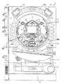
図1に示すように、パチンコ遊技機1は、額縁状に形成されたガラス扉枠2を有する。ガラス扉枠2の下部表面には打球供給皿3がある。打球供給皿3の下部には、打球供給皿3からあふれた遊技球を貯留する余剰玉受皿4と打球を発射する打球操作ハンドル(操作ノブ)5が設けられている。ガラス扉枠2の後方には、遊技盤6が着脱可能に取り付けられている。また、遊技盤6の前面には遊技領域7が設けられている。
【0026】
遊技領域7の中央付近には、複数種類の図柄を可変表示するための可変表示部(特別図柄表示装置)9と7セグメントLEDによる普通図柄表示器(普通図柄表示装置)10とを含む可変表示装置8が設けられている。可変表示部9には、例えば「左」、「中」、「右」の3つの図柄表示エリアがある。可変表示装置8の側部には、打球を導く通過ゲート11が設けられている。通過ゲート11を通過した打球は、玉出口13を経て始動入賞口14の方に導かれる。通過ゲート11と玉出口13との間の通路には、通過ゲート11を通過した打球を検出するゲートスイッチ12がある。また、始動入賞口14に入った入賞球は、遊技盤6の背面に導かれ、始動口スイッチ17によって検出される。また、始動入賞口14の下部には開閉動作を行う可変入賞球装置15が設けられている。可変入賞球装置15は、ソレノイド16によって開状態とされる。
【0027】
可変入賞球装置15の下部には、特定遊技状態(大当り状態)においてソレノイド21によって開状態とされる開閉板20が設けられている。この実施の形態では、開閉板20が大入賞口を開閉する手段となる。開閉板20から遊技盤6の背面に導かれた入賞球のうち一方(Vゾーン)に入った入賞球はVカウントスイッチ(V入賞スイッチ)22で検出される。また、開閉板20からの入賞球はカウントスイッチ23で検出される。可変表示装置8の下部には、始動入賞口14に入った入賞球数を表示する4個の表示部を有する始動入賞記憶表示器18が設けられている。この例では、4個を上限として、始動入賞がある毎に、始動入賞記憶表示器18は点灯している表示部を1つずつ増やす。そして、可変表示部9の可変表示が開始される毎に、点灯している表示部を1つ減らす。
【0028】
遊技盤6には、複数の入賞口19,24が設けられ、遊技球のそれぞれの入賞口19,24への入賞は、対応して設けられている入賞口スイッチ19a,19b,24a,24bによって検出される。遊技領域7の左右周辺には、遊技中に点滅表示される装飾ランプ25が設けられ、下部には、入賞しなかった打球を吸収するアウト口26がある。また、遊技領域7の外側の左右上部には、効果音を発する2つのスピーカ27が設けられている。遊技領域7の外周には、遊技効果LED28aおよび遊技効果ランプ28b,28cが設けられている。
【0029】
そして、この例では、一方のスピーカ27の近傍に、賞球残数があるときに点灯する賞球ランプ51が設けられ、他方のスピーカ27の近傍に、補給球が切れたときに点灯する球切れランプ52が設けられている。さらに、図1には、パチンコ遊技機1に隣接して設置され、プリペイドカードが挿入されることによって球貸しを可能にするカードユニット50も示されている。
【0030】
カードユニット50には、使用可能状態であるか否かを示す使用可表示ランプ151、カード内に記録された残額情報に端数(100円未満の数)が存在する場合にその端数を打球供給皿3の近傍に設けられる度数表示LEDに表示させるための端数表示スイッチ152、カードユニット50がいずれの側のパチンコ遊技機1に対応しているのかを示す連結台方向表示器153、カードユニット50内にカードが投入されていることを示すカード投入表示ランプ154、記録媒体としてのカードが挿入されるカード挿入口155、およびカード挿入口155の裏面に設けられているカードリーダライタの機構を点検する場合にカードユニット50を解放するためのカードユニット錠156が設けられている。
【0031】
打球発射装置から発射された打球は、打球レールを通って遊技領域7に入り、その後、遊技領域7を下りてくる。打球が通過ゲート11を通ってゲートスイッチ12で検出されると、普通図柄表示器10の表示数字が連続的に変化する状態になる。また、打球が始動入賞口14に入り始動口スイッチ17で検出されると、図柄の変動を開始できる状態であれば、可変表示部9内の図柄が回転を始める。図柄の変動を開始できる状態でなければ、始動入賞記憶を1増やす。
【0032】
可変表示部9内の画像の回転は、一定時間が経過したときに停止する。停止時の画像の組み合わせが大当り図柄の組み合わせであると、大当り遊技状態に移行する。すなわち、開閉板20が、一定時間経過するまで、または、所定個数(例えば10個)の打球が入賞するまで開放する。そして、開閉板20の開放中に打球が特定入賞領域に入賞しV入賞スイッチ22で検出されると、継続権が発生し開閉板20の開放が再度行われる。継続権の発生は、所定回数(例えば15ラウンド)許容される。
【0033】
停止時の可変表示部9内の画像の組み合わせが確率変動を伴う大当り図柄の組み合わせである場合には、次に大当りとなる確率が高くなる。すなわち、高確率状態という遊技者にとってさらに有利な状態となる。また、普通図柄表示器10における停止図柄が所定の図柄(当り図柄=小当り図柄)である場合に、可変入賞球装置15が所定時間だけ開状態になる。さらに、高確率状態では、普通図柄表示器10における停止図柄が当り図柄になる確率が高められるとともに、可変入賞球装置15の開放時間と開放回数が高められる。
【0034】
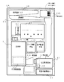
次に、パチンコ遊技機1の裏面に配置されている各基板について説明する。
図2に示すように、パチンコ遊技機1の裏面では、枠体2A内の機構板の上部に玉貯留タンク38が設けられ、パチンコ遊技機1が遊技機設置島に設置された状態でその上方から遊技球が球貯留タンク38に供給される。球貯留タンク38内の遊技球は、誘導樋39を通って賞球ケースで覆われる球払出装置に至る。
【0035】
遊技機裏面側では、可変表示部9を制御する可変表示制御ユニット29、遊技制御用マイクロコンピュータ等が搭載された遊技制御基板(主基板)31が設置されている。また、球払出制御を行う払出制御用マイクロコンピュータ等が搭載された払出制御基板37、およびモータの回転力を利用して打球を遊技領域7に発射する打球発射装置が設置されている。さらに、装飾ランプ25、遊技効果LED28a、遊技効果ランプ28b,28c、賞球ランプ51および球切れランプ52に信号を送るためのランプ制御基板35、スピーカ27からの音声発生を制御するための音声制御基板70および打球発射装置を制御するための発射制御基板91も設けられている。
【0036】
さらに、DC30V、DC21V、DC12VおよびDC5Vを作成する電源回路が搭載された電源基板910が設けられ、上方には、各種情報を遊技機外部に出力するための各端子を備えたターミナル基板160が設置されている。ターミナル基板160には、少なくとも、球切れ検出スイッチの出力を導入して外部出力するための球切れ用端子、賞球個数信号を外部出力するための賞球用端子および球貸し個数信号を外部出力するための球貸し用端子が設けられている。また、中央付近には、主基板31からの各種情報を遊技機外部に出力するための各端子を備えた情報端子盤34が設置されている。なお、図2には、ランプ制御基板35および音声制御基板70からの信号を、枠側に設けられている遊技効果LED28a、遊技効果ランプ28b,28c、賞球ランプ51および球切れランプ52に供給するための電飾中継基板A77が示されているが、信号中継の必要に応じて他の中継基板も設けられる。
【0037】
図3はパチンコ遊技機1の機構板を背面からみた背面図である。球貯留タンク38に貯留された玉は誘導樋39を通り、図3に示されるように、球切れ検出器(球切れスイッチ)187a,187bを通過して球供給樋186a,186bを経て球払出装置97に至る。球切れスイッチ187a,187bは遊技球通路内の遊技球の有無を検出するスイッチであるが、球タンク38内の補給球の不足を検出する球切れ検出スイッチ167も設けられている。以下、球切れスイッチ187a,187bを、球切れスイッチ187と表現することがある。
【0038】
球払出装置97から払い出された遊技球は、連絡口45を通ってパチンコ遊技機1の前面に設けられている打球供給皿3に供給される。連絡口45の側方には、パチンコ遊技機1の前面に設けられている余剰玉受皿4に連通する余剰玉通路46が形成されている。
【0039】
入賞にもとづく景品球が多数払い出されて打球供給皿3が満杯になり、ついには遊技球が連絡口45に到達した後さらに遊技球が払い出されると遊技球は、余剰玉通路46を経て余剰玉受皿4に導かれる。さらに遊技球が払い出されると、感知レバー47が満タンスイッチ48を押圧して満タンスイッチ48がオンする。その状態では、球払出装置97内のステッピングモータの回転が停止して球払出装置97の動作が停止するとともに打球発射装置の駆動も停止する。
【0040】
次に、機構板36に設置されている中間ベースユニットの構成について説明する。中間ベースユニットには、球供給樋186a,186bや球払出装置97が設置される。図4に示すように、中間ベースユニットの上下には連結凹突部182が形成されている。連結凹突部182は、中間ベースユニットと機構板36の上部ベースユニットおよび下部ベースユニットを連結固定するものである。
【0041】
中間ベースユニットの上部には通路体184が固定されている。そして、通路体184の下部に球払出装置97が固定されている。通路体184は、カーブ樋174(図3参照)によって流下方向を左右方向に変換された2列の遊技球を流下させる払出球通路186a,186bを有する。払出球通路186a,186bの上流側には、球切れスイッチ187a,187bが設置されている。球切れスイッチ187a,187bは、払出球通路186a,186b内の遊技球の有無を検出するものであって、球切れスイッチ187a,187bが遊技球を検出しなくなると球払出装置97における払出モータ(図4において図示せず)の回転を停止して球払出が不動化される。
【0042】
なお、球切れスイッチ187a,187bは、払出球通路186a,186bに27〜28個程度の遊技球が存在することを検出できるような位置に係止片188によって係止されている。すなわち、球切れスイッチ187a,187bは、賞球の一単位の最大払出量(この実施の形態では15個)および球貸しの一単位の最大払出量(この実施の形態では100円:25個)以上が確保されていることが確認できるような位置に設置されている。
【0043】
通路体184の中央部は、内部を流下する遊技球の球圧を弱めるように、左右に湾曲する形状に形成されている。そして、払出球通路186a,186bの間に止め穴189が形成されている。止め穴189の裏面は中間ベースユニットに設けられている取付ボスがはめ込まれる。その状態で止めねじがねじ止めされて、通路体184は中間ベースユニットに固定される。なお、ねじ止めされる前に、中間ベースユニットに設けられている係止突片185によって通路体184の位置合わせを行えるようになっている。
【0044】
通路体184の下方には、球払出装置97に遊技球を供給するとともに故障時等には球払出装置97への遊技球の供給を停止する球止め装置190が設けられている。球止め装置190の下方に設置される球払出装置97は、直方体状のケース198の内部に収納されている。ケース198の左右4箇所には突部が設けられている。各突部が中間ベースユニットに設けられている位置決め突片に係った状態で、中間ベースユニットの下部に設けられている弾性係合片にケース198の下端がはめ込まれる。
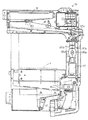
【0045】
図5は球払出装置97の分解斜視図である。球払出装置97の構成および作用について図5を参照して説明する。この実施形態における球払出装置97は、ステッピングモータ(払出モータ)289がスクリュー288を回転させることによりパチンコ玉を1個ずつ払い出す。なお、球払出装置97は、入賞にもとづく景品球だけでなく、貸し出すべき遊技球も払い出す。
【0046】
図5に示すように、球払出装置97は、2つのケース198a,198bを有する。それぞれのケース198a,198bの左右2箇所に、球払出装置97の設置位置上部に設けられた位置決め突片に当接される係合突部280が設けられている。また、それぞれのケース198a,198bには、球供給路281a,281bが形成されている。球供給路281a,281bは湾曲面282a,282bを有し、湾曲面282a,282bの終端の下方には、球送り水平路284a,284bが形成されている。さらに、球送り水平路284a,284bの終端に球排出路283a,283bが形成されている。
【0047】
球供給路281a,281b、球送り水平路284a,284b、球排出路283a,283bは、ケース198a,198bをそれぞれ前後に区画する区画壁295a,295bの前方に形成されている。また、区画壁295a,295bの前方において、玉圧緩衝部材285がケース198a,198b間に挟み込まれる。玉圧緩衝部材285は、球払出装置97に供給される玉を左右側方に振り分けて球供給路281a,281bに誘導する。
【0048】
また、玉圧緩衝部材285の下部には、発光素子(LED)286と受光素子(図示せず)とによる払出モータ位置センサが設けられている。発光素子286と受光素子とは、所定の間隔をあけて設けられている。そして、この間隔内に、スクリュー288の先端が挿入されるようになっている。なお、玉圧緩衝部材285は、ケース198a,198bが張り合わされたときに、完全にその内部に収納固定される。
【0049】
球送り水平路284a,284bには、払出モータ289によって回転させられるスクリュー288が配置されている。払出モータ289はモータ固定板290に固定され、モータ固定板290は、区画壁295a,295bの後方に形成される固定溝291a,291bにはめ込まれる。その状態で払出モータ289のモータ軸が区画壁295a,295bの前方に突出するので、その突出の前方にスクリュー288が固定される。スクリュー288の外周には、払出モータ289の回転によって球送り水平路284a,284bに載置された遊技球を前方に移動させるための螺旋突起288aが設けられている。
【0050】
そして、スクリュー288の先端には、発光素子286を収納するように凹部が形成され、その凹部の外周には、2つの切欠部292が互いに180度離れて形成されている。従って、スクリュー288が1回転する間に、発光素子286からの光は、切欠部292を介して受光素子で2回検出される。
【0051】
つまり、発光素子286と受光素子とによる払出モータ位置センサは、スクリュー288を定位置で停止するためのものであり、かつ、払出動作が行われた旨を検出するものである。なお、発光素子286、受光素子および払出モータ289からの配線は、まとめられてケース198a,198bの後部下方に形成された引出穴から外部に引き出されコネクタに結線される。
【0052】
遊技球が球送り水平路284a,284bに載置された状態において、払出モータ289が回転すると、スクリュー288の螺旋突起288aによって、遊技球は、球送り水平路284a,284b上を前方に向かって移動する。そして、遂には、球送り水平路284a,284bの終端から球排出路283a,283bに落下する。このとき、左右の球送り水平路284a,284bからの落下は交互に行われる。すなわち、スクリュー288が半回転する毎に一方から1個の遊技球が落下する。従って、1個の遊技球が落下する毎に、発光素子286からの光が受光素子によって検出される。
【0053】
図4に示すように、球払出装置97の下方には、球振分部材(切替部材)311が設けられている。球振分部材311は、振分ソレノイド310によって駆動される。例えば、ソレノイド310のオン時には、球振分部材311は右側に倒れ、オフ時には左側に倒れる。振分ソレノイド310の下方には、近接スイッチによる賞球カウントスイッチ301Aおよび球貸しカウントスイッチ301Bが設けられている。入賞にもとづく賞球時には、球振分部材311は右側に倒れ、球排出路283a,283bからの玉はともに賞球カウントスイッチ301Aを通過する。また、球貸し時には、球振分部材311は左側に倒れ、球排出路283a,283bからの玉はともに球貸しカウントスイッチ301Bを通過する。従って、球払出装置97は、賞球時と球貸し時とで払出流下路を切り替えて、所定数の遊技媒体の払出を行うことができる。
【0054】
このように、球振分部材311を設けることによって、2条の玉流路を落下してきた玉は、賞球カウントスイッチ301Aと球貸しカウントスイッチ301Bとのうちのいずれか一方しか通過しない。従って、賞球であるのか球貸しであるのかの判断をすることなく、賞球カウントスイッチ301Aと球貸しカウントスイッチ301Bの検出出力から、直ちに賞球数または球貸し数を把握することができる。
【0055】
なお、この実施の形態では、電気的駆動源の駆動によって遊技球を払い出す球払出装置として、ステッピングモータの回転によって遊技球が払い出される球払出装置97を用いることにするが、その他の駆動源によって遊技球を送り出す構造の球払出装置を用いてもよいし、ソレノイド等の電気的駆動源の駆動によってストッパを外し遊技球の自重によって払い出しがなされる構造の球払出装置を用いてもよい。また、この実施の形態では、球払出装置97は賞球にもとづく景品球と貸出要求にもとづく貸し球の双方を払い出すが、それぞれについて払出装置が設けられていてもよい。
【0056】
図6は、主基板31における回路構成の一例を示すブロック図である。なお、図6には、払出制御基板37、ランプ制御基板35、音声制御基板70、発射制御基板91および図柄制御基板80も示されている。主基板31には、プログラムに従ってパチンコ遊技機1を制御する基本回路53と、ゲートスイッチ12、始動口スイッチ17、V入賞スイッチ22、カウントスイッチ23、入賞口スイッチ19a,19b,24a,24b、満タンスイッチ48、球切れスイッチ187および賞球カウントスイッチ301Aからの信号を基本回路53に与えるスイッチ回路58と、可変入賞球装置15を開閉するソレノイド16、開閉板20を開閉するソレノイド21および大入賞口内の経路を切り換えるためのソレノイド21Aを基本回路53からの指令に従って駆動するソレノイド回路59とが搭載されている。
【0057】
なお、図6には示されていないが、カウントスイッチ短絡信号もスイッチ回路58を介して基本回路53に伝達される。
【0058】
また、基本回路53から与えられるデータに従って、大当りの発生を示す大当り情報、可変表示部9の画像表示開始に利用された始動入賞球の個数を示す有効始動情報、確率変動が生じたことを示す確変情報等の情報出力信号をホールコンピュータ等の外部機器に対して出力する情報出力回路64が搭載されている。
【0059】
基本回路53は、ゲーム制御用のプログラム等を記憶するROM54、ワークメモリとして使用される記憶手段(変動データを記憶する手段)の一例であるRAM55、プログラムに従って制御動作を行うCPU56およびI/Oポート部57を含む。この実施の形態では、ROM54,RAM55はCPU56に内蔵されている。すなわち、CPU56は、1チップマイクロコンピュータである。なお、1チップマイクロコンピュータは、少なくともRAM55が内蔵されていればよく、ROM54およびI/Oポート部57は外付けであっても内蔵されていてもよい。
【0060】
遊技球を打撃して発射する打球発射装置は発射制御基板91上の回路によって制御される駆動モータ94で駆動される。そして、駆動モータ94の駆動力は、操作ノブ5の操作量に従って調整される。すなわち、発射制御基板91上の回路によって、操作ノブ5の操作量に応じた速度で打球が発射されるように制御される。
【0061】
この実施の形態では、電源基板910から主基板31に対して、ローレベルがリセット状態を示すリセット信号、ローアクティブの復帰信号およびローアクティブの電源断信号も入力される。リセット信号と復帰信号とはAND回路161に入力され、AND回路161の出力がCPU56のリセット端子に入力される。また、電源断信号は、CPU56のマスク不能割込(NMI)端子に入力される。さらに、図6には明示されていないが、RAM(CPU内蔵RAMであってもよい。)55の一部または全部が、電源基板910において作成されるバックアップ電源よってバックアップされているバックアップRAMである。すなわち、遊技機に対する電力供給が停止しても、所定期間は、RAM55の一部または全部の内容は保存される。
【0062】
なお、この実施の形態では、ランプ制御基板35に搭載されているランプ制御手段が、遊技盤に設けられている始動記憶表示器18、ゲート通過記憶表示器41および装飾ランプ25の表示制御を行うとともに、枠側に設けられている遊技効果ランプ・LED28a,28b,28c、賞球ランプ51および球切れランプ52の表示制御を行う。また、特別図柄を可変表示する可変表示部9および普通図柄を可変表示する普通図柄表示器10の表示制御は、図柄制御基板80に搭載されている表示制御手段によって行われる。
【0063】
図7は、払出制御基板37および球払出装置97の構成要素などの払出に関連する構成要素を示すブロック図である。図7に示すように、満タンスイッチ48からの検出信号は、中継基板71を介して主基板31のI/Oポート部57に入力される。満タンスイッチ48は、余剰球受皿4の満タンを検出するスイッチである。また、球切れスイッチ187(187a,187b)からの検出信号も、中継基板72および中継基板71を介して主基板31のI/Oポート部57に入力される。
【0064】
主基板31のCPU56は、球切れスイッチ187からの検出信号が球切れ状態を示しているか、または、満タンスイッチ48からの検出信号が満タン状態を示していると、払出禁止を指示する払出制御コマンドを送出する。払出禁止を指示する払出制御コマンドを受信すると、払出制御基板37の払出制御用CPU371は球払出処理を停止する。
【0065】
さらに、賞球カウントスイッチ301Aからの検出信号は、中継基板72および中継基板71を介して主基板31のI/Oポート部57に入力されるとともに、中継基板72を介して払出制御基板37の入力ポート372bに入力される。賞球カウントスイッチ301Aは、球払出装置97の払出機構部分に設けられ、実際に払い出された賞球払出球を検出する。
【0066】
入賞があると、払出制御基板37には、主基板31の出力ポート(ポート0,1)570,571から賞球個数を示す払出制御コマンドが入力される。出力ポート(出力ポート1)571は8ビットのデータを出力し、出力ポート570は1ビットのストローブ信号(INT信号)を出力する。賞球個数を示す払出制御コマンドは、入力バッファ回路373Aを介してI/Oポート372aに入力される。INT信号は、入力バッファ回路373Bを介して払出制御用CPU371の割込端子に入力されている。払出制御用CPU371は、I/Oポート372aを介して払出制御コマンドを入力し、払出制御コマンドに応じて球払出装置97を駆動して賞球払出を行う。なお、この実施の形態では、払出制御用CPU371は、1チップマイクロコンピュータであり、少なくともRAMが内蔵されている。
【0067】
また、主基板31において、出力ポート570,571の外側にバッファ回路620,68Aが設けられている。バッファ回路620,68Aとして、例えば、汎用のCMOS−ICである74HC250,74HC14が用いられる。このような構成によれば、外部から主基板31の内部に入力される信号が阻止されるので、払出制御基板37から主基板31に信号が与えられる可能性がある信号ラインをさらに確実になくすことができる。なお、バッファ回路620,68Aの出力側にノイズフィルタを設けてもよい。
【0068】
払出制御用CPU371は、出力ポート372cを介して、貸し球数を示す球貸し個数信号をターミナル基板160に出力する。さらに、出力ポート372dを介して、エラー表示用LED374にエラー信号を出力する。
【0069】
さらに、払出制御基板37の入力ポート372bには、中継基板72を介して球貸しカウントスイッチ301Bからの検出信号が入力される。球貸しカウントスイッチ301Bは、球払出装置97の払出機構部分に設けられ、実際に払い出された貸し球を検出する。払出制御基板37からの払出モータ289への駆動信号はあ、出力ポート372cおよび中継基板72を介して球払出装置97の払出機構部分における払出モータ289に伝えられ、振分ソレノイド310への駆動信号は、出力ポート372eおよび中継基板72を介して球払出装置97の払出機構部分における振分ソレノイド310に伝えられる。
【0070】
カードユニット50には、カードユニット制御用マイクロコンピュータが搭載されている。また、カードユニット50には、端数表示スイッチ152、連結台方向表示器153、カード投入表示ランプ154およびカード挿入口155が設けられている(図1参照)。残高表示基板74には、打球供給皿3の近傍に設けられている度数表示LED、球貸しスイッチおよび返却スイッチが接続される。
【0071】
残高表示基板74からカードユニット50には、遊技者の操作に応じて、球貸しスイッチ信号および返却スイッチ信号が払出制御基板37を介して与えられる。また、カードユニット50から残高表示基板74には、プリペイドカードの残高を示すカード残高表示信号および球貸し可表示信号が払出制御基板37を介して与えられる。カードユニット50と払出制御基板37の間では、接続信号(VL信号)、ユニット操作信号(BRDY信号)、球貸し要求信号(BRQ信号)、球貸し完了信号(EXS信号)およびパチンコ機動作信号(PRDY信号)が入力ポート372bおよび出力ポート372eを介してやりとりされる。
【0072】
パチンコ遊技機1の電源が投入されると、払出制御基板37の払出制御用CPU371は、カードユニット50にPRDY信号を出力する。また、カードユニット制御用マイクロコンピュータは、VL信号を出力する。払出制御用CPU371は、VL信号の入力状態により接続状態/未接続状態を判定する。カードユニット50においてカードが受け付けられ、球貸しスイッチが操作され球貸しスイッチ信号が入力されると、カードユニット制御用マイクロコンピュータは、払出制御基板37にBRDY信号を出力する。この時点から所定の遅延時間が経過すると、カードユニット制御用マイクロコンピュータは、払出制御基板37にBRQ信号を出力する。
【0073】
そして、払出制御基板37の払出制御用CPU371は、カードユニット50に対するEXS信号を立ち上げ、カードユニット50からのBRQ信号の立ち下がりを検出すると、払出モータ289を駆動し、所定個の貸し球を遊技者に払い出す。このとき、振分ソレノイド310は駆動状態とされている。すなわち、球振分部材311を球貸し側に向ける。そして、払出が完了したら、払出制御用CPU371は、カードユニット50に対するEXS信号を立ち下げる。その後、カードユニット50からのBRDY信号がオン状態でなければ、賞球払出制御を実行する。
【0074】
以上のように、カードユニット50からの信号は全て払出制御基板37に入力される構成になっている。従って、球貸し制御に関して、カードユニット50から主基板31に信号が入力されることはなく、主基板31の基本回路53にカードユニット50の側から不正に信号が入力される余地はない。
【0075】
この実施の形態では、電源基板910から払出制御基板37に対して、リセット信号、復帰信号および電源断信号も入力される。リセット信号と復帰信号とはAND回路385に入力され、AND回路385の出力が払出制御用CPU371のリセット端子に入力される。また、電源断信号は、払出制御用CPU371のマスク不能割込(NMI)端子に入力される。さらに、払出制御基板37に存在するRAM(CPU内蔵RAMであってもよい。)の少なくとも一部は、電源基板910において作成されるバックアップ電源によって、バックアップされている。すなわち、遊技機に対する電力供給が停止しても、所定期間は、RAMの少なくとも一部の内容は保存される。
【0076】
なお、この実施の形態では、カードユニット50が遊技機とは別体として遊技機に隣接して設置されている場合を例にするが、カードユニット50は遊技機と一体化されていてもよい。また、コイン投入に応じてその金額に応じた遊技球が貸し出されるような場合でも本発明を適用できる。
【0077】
図8は、電源基板910の一構成例を示すブロック図である。電源基板910は、主基板31、図柄制御基板80、音声制御基板70、ランプ制御基板35および払出制御基板37等の電気部品制御基板と独立して設置され、遊技機内の各電気部品制御基板および機構部品が使用する電圧を生成する。この例では、AC24V、VSL(DC+30V)、DC+21V、DC+12VおよびDC+5Vを生成する。また、バックアップ電源となるコンデンサ916は、DC+5Vすなわち各基板上のIC等を駆動する電源のラインから充電される。なお、VSLは、整流回路912において、整流素子でAC24Vを整流昇圧することによって生成される。VSLは、ソレノイド駆動電源となる。
【0078】
トランス911は、交流電源からの交流電圧を24Vに変換する。AC24V電圧は、コネクタ915に出力される。また、整流回路912は、AC24Vから+30Vの直流電圧を生成し、DC−DCコンバータ913およびコネクタ915に出力する。DC−DCコンバータ913は、1つまたは複数のコンバータIC922(図8では1つのみを示す。)を有し、VSLにもとづいて+21V、+12Vおよび+5Vを生成してコネクタ915に出力する。コンバータIC922の入力側には、比較的大容量のコンデンサ923が接続されている。従って、外部からの遊技機に対する電力供給が停止したときに、+30V、+12V、+5V等の直流電圧は、比較的緩やかに低下する。この結果、コンデンサ923は、後述する補助駆動電源の役割を果たす。コネクタ915は例えば中継基板に接続され、中継基板から各電気部品制御基板および機構部品に必要な電圧の電力が供給される。
【0079】
ただし、電源基板910に各電気部品制御基板に至る各コネクタを設け、電源基板910から、中継基板を介さずにそれぞれの基板に至る各電圧を供給するようにしてもよい。また、図8には1つのコネクタ915が代表して示されているが、コネクタは、各電気部品制御基板対応に設けられている。
【0080】
DC−DCコンバータ913からの+5Vラインは分岐してバックアップ+5Vラインを形成する。バックアップ+5Vラインとグラウンドレベルとの間には大容量のコンデンサ916が接続されている。コンデンサ916は、遊技機に対する電力供給が遮断されたときの電気部品制御基板のバックアップRAM(電源バックアップされているRAMすなわち電力供給停止時にも記憶内容保持状態となりうるバックアップ記憶手段)に対して記憶状態を保持できるように電力を供給するバックアップ電源となる。また、+5Vラインとバックアップ+5Vラインとの間に、逆流防止用のダイオード917が挿入される。この実施の形態では、バックアップ用の+5Vは、主基板31および払出制御基板37に供給される。
【0081】
なお、バックアップ電源として、+5V電源から充電可能な電池を用いてもよい。電池を用いる場合には、+5V電源から電力供給されない状態が所定時間継続すると容量がなくなるような充電池が用いられる。
【0082】
また、電源基板910には、電源監視用IC902が搭載されている。電源監視用IC902は、VSL電圧を導入し、VSL電圧を監視することによって電源断の発生を検出する。具体的には、VSL電圧が所定値(この例では+22V)以下になったら、電源断が生ずるとして電源断信号を出力する。なお、監視対象の電源電圧は、各電気部品制御基板に搭載されている回路素子の電源電圧(この例では+5V)よりも高い電圧であることが好ましい。この例では、交流から直流に変換された直後の電圧であるVSLが用いられている。電源監視用IC902からの電源断信号は、主基板31や払出制御基板37等に供給される。
【0083】
電源監視用IC902が電源断を検知するための所定値は、通常時の電圧より低いが、各電気部品制御基板上のCPUが暫くの間動作しうる程度の電圧である。また、電源監視用IC902が、CPU等の回路素子を駆動するための電圧(この例では+5V)よりも高く、また、交流から直流に変換された直後の電圧を監視するように構成されているので、CPUが必要とする電圧に対して監視範囲を広げることができる。従って、より精密な監視を行うことができる。さらに、監視電圧としてVSL(+30V)を用いる場合には、遊技機の各種スイッチに供給される電圧が+12Vであることから、電源瞬断時のスイッチオン誤検出の防止も期待できる。すなわち、+30V電源の電圧を監視すると、+30V作成の以降に作られる+12Vが落ち始める以前の段階でそれの低下を検出できる。
【0084】
よって、+12V電源の電圧が低下するとスイッチ出力がオン状態を呈するようになるが、+12Vより早く低下する+30V電源電圧を監視して電源断を認識すれば、スイッチ出力がオン状態を呈する前に電源復旧待ちの状態に入ってスイッチ出力を検出しない状態となることができる。
【0085】
また、電源監視用IC902は、電気部品制御基板とは別個の電源基板910に搭載されているので、電源監視回路から複数の電気部品制御基板に電源断信号を供給することができる。電源断信号を必要とする電気部品制御基板が幾つあっても電源監視手段は1つ設けられていればよいので、各電気部品制御基板における各電気部品制御手段が後述する復帰制御を行っても、遊技機のコストはさほど上昇しない。
【0086】
なお、図8に示された構成では、電源監視用IC902の検出出力(電源断信号)は、バッファ回路918,919を介してそれぞれの電気部品制御基板(例えば主基板31と払出制御基板37)に伝達されるが、例えば、1つの検出出力を中継基板に伝達し、中継基板から各電気部品制御基板に同じ信号を分配する構成でもよい。また、電源断信号を必要とする基板数に応じたバッファ回路を設けてもよい。
【0087】
さらに、電源基板910には、各基板にリセット信号および復帰信号を供給するリセット管理回路940が搭載されている。リセット管理回路940は、起動順序制御手段の一実現例である。
【0088】
図9は、リセット管理回路940の構成例を示すブロック図である。リセット管理回路940において、リセット回路65におけるリセットIC651は、電源投入時に、外付けのコンデンサの容量で決まる所定時間だけ出力をローレベルとし、所定時間が経過すると出力をハイレベルにする。リセットIC651の出力は、リセット信号回路950における各回路941〜949を介して、バッファ回路961〜964および遅延回路960に供給される。遅延回路960の出力はバッファ回路965に入力する。そして、バッファ回路961〜965が各電気部品制御基板にリセット信号として供給される。従って、リセットIC651の出力がハイレベルになると、各電気部品制御基板におけるCPUが動作可能状態になる。
【0089】
また、リセットIC651は、電源監視用IC902が監視する電源電圧と等しい電源電圧であるVSLの電源電圧を監視して電圧値が所定値(電源監視用IC902が電源断信号を出力する電源電圧値よりも低い値)以下になるとローレベルになる。従って、CPU56および払出制御用CPU371は、電源監視用IC902からの電源断信号に応じて所定の電力供給停止準備処理を行った後、システムリセットされることになる。
【0090】
図9に示すように、リセットIC651からのリセット信号は、NAND回路947に入力されるとともに、反転回路(NOT回路)944を介してカウンタIC941のクリア端子に入力される。カウンタIC941は、クリア端子への入力がローレベルになると、発振器943からのクロック信号をカウントする。そして、カウンタIC941のQ5出力がNOT回路945,946を介してNAND回路947に入力される。
【0091】
また、カウンタIC941のQ6出力は、フリップフロップ(FF)942のクロック端子に入力される。フリップフロップ942のD入力はハイレベルに固定され、Q出力は論理和回路(OR回路)949に入力される。OR回路949の他方の入力には、NAND回路947の出力がNOT回路948を介して導入される。そして、OR回路949の出力が、バッファ回路961〜965を介して各CPUに供給されている。このような構成によれば、電源投入時に、各CPUのリセット端子に2回のリセット信号(ローレベル信号)が与えられるので、各CPUは、確実に動作を開始する。
【0092】
そして、例えば、電源監視手段である電源監視用IC902の検出電圧(電源断信号を出力することになる電圧)を+22Vとし、リセットIC651の検出電圧を+9Vとする。そのように構成した場合には、電源監視手段とリセットIC651とは、同一の電源VSLの電圧を監視するので、電源監視手段が電源断信号を出力するタイミングとリセットIC651がリセットレベルであるローレベルを出力するタイミングとの差を所望の所定期間に確実に設定することができる。所望の所定期間とは、電源監視手段からの電源断信号に応じて電力供給停止準備処理(電力供給停止時処理)を開始してから、その処理が確実に完了するまでの期間である。
【0093】
この例では、電源監視手段が検出信号を出力することになる検出条件は+30V電源電圧が+22Vにまで低下したことであり、リセットIC651がリセットレベルであるローレベルを出力することになる条件は+30V電源電圧が+9Vにまで低下したことになる。ただし、ここで用いられている電圧値は一例であって、他の値を用いてもよい。
【0094】
ただし、監視範囲が狭まるが、電源監視手段およびリセットIC651の監視電圧として+5V電源電圧を用いることも可能である。その場合にも、電源監視回路の検出電圧は、リセットIC651の検出電圧よりも高く設定される。
【0095】
主基板31および払出制御基板37のCPU56および払出制御用CPU371の駆動電源である+5V電源から電力が供給されていない間、RAMの少なくとも一部は、電源基板910から供給されるバックアップ電源によってバックアップされ、遊技機に対する電源が断しても内容は保存される。そして、電源が復旧すると、リセット管理回路940からのリセット信号がハイレベルになるので、CPU56および払出制御用CPU371は、通常の動作状態に復帰する。そのとき、必要なデータがバックアップRAMに保存されているので、停電等からの復旧時に停電発生時の遊技状態に復帰することができる。
【0096】
なお、図9には、電源投入時に各電気部品制御基板のCPUのリセット端子に2回のリセット信号(ローレベル信号)が与えられる構成が示されたが、リセット信号の立ち上がりタイミングが1回しかなくても確実にリセット解除されるCPUを使用する場合には、符号941〜949で示された回路素子は不要である。その場合、リセットIC651の出力がそのままバッファ回路961〜964および遅延回路960に接続される。
【0097】
また、この実施の形態では、電源基板910から各電気部品制御基板のCPUにリセット信号が供給されるときに、遅延回路960が、主基板31のCPU56に対するリセット信号を遅延させる。従って、電源投入時に、主基板31のCPU56に対するリセット信号は、他の電気部品制御基板のCPUに対するリセット信号よりも遅く立ち上がる。
【0098】
例えば、主基板31のCPU56が他の電気部品制御基板に対して制御コマンドを出力する際に、他の電気部品制御基板におけるCPUは既に立ち上がっているので、制御コマンドは確実に受信側の電気部品制御基板のCPUで受信される。
【0099】
さらに、電源基板910には、待機期間を計測して復帰信号を出力する復帰信号出力手段の一例であるカウンタ971が搭載されている。カウンタ971は、電源断信号がローレベルになってクリアが解けると、発振器943からのクロック信号をカウントする。そして、カウントアップすると、Q出力として、ハイレベルの1パルスを発生する。そのパルス信号は反転回路972で論理反転され、バッファ回路973および遅延回路974に入力する。遅延回路974は、入力信号を所定期間遅延させてバッファ回路975に入力させる。
【0100】
バッファ回路973の出力は、払出制御基板37への復帰信号となる。また、バッファ回路975の出力は、主基板31への復帰信号となる。なお、バッファ回路973,975は、払出制御基板37、主基板31に設けられていてもよい。
【0101】
図10は、主基板31におけるCPU56周りの一構成例を示すブロック図である。図10に示すように、電源基板910の電源監視回路(電源監視手段)からの電源断信号が、CPU56のマスク不能割込端子(XNMI端子)に接続されている。上述したように、電源監視回路は、遊技機が使用する各種直流電源のうちのいずれかの電源の電圧を監視して電源電圧低下を検出する回路である。この実施の形態では、VSLの電源電圧を監視して電圧値が所定値以下になるとローレベルの電源断信号を発生する。VSLは、遊技機における直流電圧のうちで最大のものであり、この例では+30Vである。従って、CPU56は、割込処理によって電源断の発生を確認することができる。
【0102】
また、図10に示すように、電源基板910からのリセット信号と復帰信号とはAND回路161に入力され、AND回路161の出力がCPU56のリセット端子(リセット信号入力部)に入力される。
【0103】
図11は、図9に示されたリセット回路65のリセットIC651とリセット信号回路950における各ICの出力信号の様子を示すタイミング図である。図11示すように、リセットIC651の出力は、+5V電源電圧のレベルが所定値を越えるとハイレベルになる。リセットIC651の出力がハイレベルになると、カウンタIC941のクリア状態が解除されるので、カウンタIC941は発振器943の出力クロック信号のカウントを開始する。発振器943の発振周波数は例えば11.776MHzである。
【0104】
カウンタIC941が16クロックをカウントするとQ5出力が立ち上がる。また、32クロックをカウントするとQ6出力がハイレベルに立ち上がる。カウンタIC941のQ6出力が立ち上がると、FF942の出力がハイレベルになる。IC947は、カウンタIC941のQ6出力とリセットIC651の出力との論理積を反転して、図11に示すような信号を出力する。OR回路949は、IC947の出力を反転するIC948の出力とFF942の出力との論理和をとって、図11に示すような信号を出力する。
【0105】
従って、遊技機の電源オン時には、各電気部品制御基板のCPUのリセット端子に対して、一旦リセット解除状態(ハイレベル)になってから、再度リセット状態(ローレベル)になるような信号が供給される。すなわち、電源オン時には、CPUのリセット端子に、リセット解除を示すレベルとなった後に再度リセットレベルに立ち下がり、その後リセット解除を示すレベルとなる信号が与えられる。その結果、CPUは、最初のリセット解除を示すローレベルからハイレベルへの変化によって起動しなかったとしても、2回目のローレベルからハイレベルへの変化によって確実に起動することができる。よって、遊技機の電源投入時に、確実に制御が開始される。
【0106】
このように、この実施の形態では、いうなればCPUの状態が安定してからリセット解除されることになる。そのようなリセット制御によって、CPUは確実にシステムリセットの後に起動する。
【0107】
なお、IC949が出力するハイレベルパルス(リセット解除状態に相当)およびローレベルパルス(リセット状態に相当)の幅は、カウンタIC941の出力端子を変更するによって任意に設定することができる。ただし、IC949が出力するハイレベルパルスの幅は、発振器943の出力クロックの数クロック分(例えば4クロック)以上であることが好ましいが、この例では、16クロック分となっている。また、IC949が出力するローレベルパルスの幅は、発振器943の出力クロックの数クロック分(例えば4クロック)以上であることが好ましいが、この例では、16クロック分となっている。
【0108】
電気部品制御基板に搭載されているCPUは、リセット状態が解除されて動作を開始すると、本来の遊技制御処理を開始する前に、セキュリティチェックなどの所定の起動時処理を行うように構成されている場合がある。すると、IC949が出力するハイレベルパルスの終了時点(立ち下がり時点)は、所定の起動時処理の完了前(本来の遊技制御処理開始前)であることが望ましい。さもないと、IC949の出力が立ち上がって所定の起動時処理が行われ、さらに本来の遊技制御処理が開始されてからIC949の出力がローレベルになることになり、本来の遊技処理開始後に、再度CPUがリセットされる状況になるからである。IC949が出力するハイレベルパルスの終了時点(立ち下がり時点)は、例えば立ち上がり時点から100ms以内であることが好ましいが、図11に示された回路構成では、100ms以内になっている。
【0109】
さらに、図12に示すように、電源基板910に搭載されているリセットIC651の出力がリセット解除を示すレベルとなる電圧を、マイクロコンピュータが動作可能な電圧レベル以上に設定することによってマイクロコンピュータの起動を確実化するようにしてもよい。図12に示す例では、リセットIC651はVSL(+30V)のレベルが+22Vになると、その出力をリセット解除を示すレベルにする。
【0110】
また、図13に示すように、システムリセット手段を構成するリセット回路65におけるリセットIC651とリセット信号回路950が作成する信号を遅延させてCPU56および他のCPUのリセット端子に供給するための遅延回路951を設けてもよい。
【0111】
以上のような制御によれば、システムリセット手段がCPUに対して最初にリセット解除を示すレベルを与えるタイミングを、電源電圧がCPUの動作保証電圧になった時点とすることも保証される。換言すれば、CPUに供給される電源がCPUが動作可能な電圧レベル以上の電圧レベルとなったことを条件にリセット解除を示すレベルを与えるように、システムリセット手段を構成することができる。従って、電源投入時等に2回以上のリセットレベルが与えられないと確実に動作し得ないCPUを用いた場合でも、2回目のリセットが、電源電圧がCPUの動作保証電圧になった時点以降に与えられる。
【0112】
次に遊技機の動作について説明する。
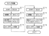
図14は、主基板31におけるCPU56が実行するメイン処理を示すフローチャートである。遊技機に対する電源が投入されると、メイン処理において、CPU56は、まず、必要な初期設定を行う。
【0113】
初期設定処理において、CPU56は、まず、割込禁止に設定する(ステップS1)。次に、割込モードを割込モード2に設定し(ステップS2)、スタックポインタにスタックポインタ指定アドレスを設定する(ステップS3)。そして、内蔵デバイスレジスタの初期化を行う(ステップS4)。また、内蔵デバイス(内蔵周辺回路)であるCTC(カウンタ/タイマ)およびPIO(パラレル入出力ポート)の初期化(ステップS5)を行った後、RAMをアクセス可能状態に設定する(ステップS6)。
【0114】
この実施の形態で用いられているCPU56には、マスク可能な割込(INT)のモードとして以下の3種類のモードが用意されている。なお、マスク可能な割込が発生すると、CPU56は、自動的に割込禁止状態に設定するとともに、プログラムカウンタの内容をスタックにセーブする。
【0115】
割込モード0:割込要求を行った内蔵デバイスがRST命令(1バイト)またはCALL命令(3バイト)をCPUの内部データバス上に送出する。よって、CPU56は、RST命令に対応したアドレスまたはCALL命令で指定されるアドレスの命令を実行する。リセット時に、CPU56は自動的に割込モード0になる。よって、割込モード1または割込モード2に設定したい場合には、初期設定処理において、割込モード1または割込モード2に設定するための処理を行う必要がある。
【0116】
割込モード1:割込が受け付けられると、常に0038(h)番地に飛ぶモードである。
【0117】
割込モード2:CPU56の特定レジスタ(Iレジスタ)の値(1バイト)と内蔵デバイスが出力する割込ベクタ(1バイト:最下位ビット0)から合成されるアドレスが、割込番地を示すモードである。すなわち、割込番地は、上位アドレスが特定レジスタの値とされ下位アドレスが割込ベクタとされた2バイトで示されるアドレスである。従って、任意の(飛び飛びではあるが)偶数番地に割込処理を設置することができる。各内蔵デバイスは割込要求を行うときに割込ベクタを送出する機能を有している。
【0118】
よって、割込モード2に設定されると、各内蔵デバイスからの割込要求を容易に処理することが可能になり、また、プログラムにおける任意の位置に割込処理を設置することが可能になる。さらに、割込モード1とは異なり、割込発生要因毎のそれぞれの割込処理を用意しておくことも容易である。上述したように、この実施の形態では、初期設定処理のステップS2において、CPU56は割込モード2に設定される。
【0119】
次いで、CPU56は、電源断時にバックアップRAM領域のデータ保護処理(例えばパリティデータの付加等の停電発生NMI処理)が行われたか否か確認する(ステップS8)。この実施の形態では、不測の電源断が生じた場合には、バックアップRAM領域のデータを保護するための処理が行われている。そのような保護処理が行われていた場合をバックアップありとする。バックアップなしを確認したら、CPU56は初期化処理を実行する。
【0120】
この実施の形態では、バックアップRAM領域にバックアップデータがあるか否かは、電源断時にバックアップRAM領域に設定されるバックアップフラグの状態によって確認される。この例では、図15に示すように、バックアップフラグ領域に「55H」が設定されていればバックアップあり(オン状態)を意味し、「55H」以外の値が設定されていればバックアップなし(オフ状態)を意味する。
【0121】
バックアップありを確認したら、CPU56は、バックアップRAM領域のデータチェック(この例ではパリティチェック)を行う。
【0122】
図16は、ステップS9のパリティチェック処理の一例を示すフローチャートである。パリティチェック処理では、CPU56は、まず、RAM55におけるバックアップパリティデータ領域に設定されているデータが「00」であるか否か確認する(ステップS9a)。バックアップパリティデータ領域については後で詳しく説明する。バックアップパリティデータ領域に設定されているデータが「00」でなければ、パリティ診断(チェックサム確認)を行う(ステップS9b)。そして、チェックサム確認の結果が正当であれば(ステップS9c)、CPU56は、後述する停電復旧処理を実行する(ステップS10)。また、チェックサム確認の結果が正当でなければ、または、バックアップパリティデータ領域に設定されているデータが「00」であった場合には、通常の初期化処理を実行する(ステップS11〜S15)。
【0123】
不測の電源断が生じた後に復旧した場合には、バックアップRAM領域のデータは保存されていたはずであるから、チェック結果は正常になる。チェック結果が正常でない場合には、内部状態を電源断時の状態に戻すことができないので、停電復旧時でない電源投入時に実行される初期化処理を実行する。
【0124】
チェック結果が正常であれば(ステップS9)、CPU56は、遊技制御手段の内部状態と表示制御手段等の電気部品制御手段の制御状態を電源断時の状態に戻すための遊技状態復旧処理を行う(ステップS10)。そして、バックアップRAM領域に保存されていたPC(プログラムカウンタ)の退避値がPCに設定され、そのアドレスに復帰する。
【0125】
なお、この実施の形態では、ステップS8でバックアップデータの有無が確認された後、バックアップデータが存在する場合にステップS9でバックアップ領域のチェックが行われたが、逆に、バックアップ領域のチェック結果が正常であったことが確認された後、バックアップデータの有無の確認を行うようにしてもよい。また、バックアップデータの有無の確認、またはバックアップ領域のチェックの何れか一方の確認を行うことによって、停電復旧処理を実行するか否かを判定してもよい。
【0126】
また、例えば停電復旧処理を実行するか否か判断する場合のパリティチェック(ステップS9)の際に、すなわち、遊技状態を復旧するか否か判断する際に、保存されていたRAMデータにおける特別プロセスフラグ等や始動入賞記憶数データによって、遊技機が遊技待機状態(図柄変動中でなく、大当り遊技中でなく、確変中でなく、また、始動入賞記憶がない状態)であることが確認されたら、遊技状態復旧処理を行わずに初期化処理を実行するようにしてもよい。
【0127】
以上のように、この実施の形態では、電力供給開始時に、電力供給停止時にバックアップRAM領域に記憶されたチェックデータ(チェックサムデータ)にもとづいて、初期化処理を行うか遊技状態復旧処理を行うかを決定するように構成したので、停電等の不測の電源断が発生したときに必要なデータを確実に保存することができ、さらに、保存されていたデータを電源復帰後に確実に活用することができる。
【0128】
通常の初期化処理(ステップS11〜S15)において、CPU56は、まず、RAMクリア処理を行う(ステップS11)。また、所定の作業領域(例えば、普通図柄判定用乱数カウンタ、普通図柄判定用バッファ、特別図柄左中右図柄バッファ、払出コマンド格納ポインタなど)に初期値を設定する初期値設定処理も行われる。さらに、サブ基板(ランプ制御基板35、払出制御基板37、音声制御基板70、図柄制御基板80)を初期化するための処理を実行する(ステップS13)。サブ基板を初期化する処理とは、例えば初期設定コマンドを送出する処理である。
【0129】
そして、2ms毎に定期的にタイマ割込がかかるようにCPU56に設けられているCTCのレジスタの設定が行われる(ステップS14)。すなわち、初期値として2msに相当する値が所定のレジスタ(時間定数レジスタ)に設定される。そして、初期設定処理のステップS1において割込禁止とされているので、初期化処理を終える前に割込が許可される(ステップS15)。
【0130】
この実施の形態では、CPU56の内蔵CTCが繰り返しタイマ割込を発生するように設定される。この実施の形態では、繰り返し周期は2msに設定される。そして、タイマ割込が発生すると、図17に示すように、CPU56は、例えばタイマ割込が発生したことを示すタイマ割込フラグをセットする(ステップS12)。
【0131】
初期化処理の実行(ステップS11〜S15)が完了すると、メイン処理で、タイマ割込が発生したか否かの監視(ステップS17)の確認が行われるループ処理に移行する。なお、ループ内では、表示用乱数更新処理(ステップS16)も実行される。
【0132】
CPU56は、ステップS17において、タイマ割込が発生したことを認識すると、ステップS21〜S31の遊技制御処理を実行する。遊技制御処理において、CPU56は、まず、スイッチ回路58を介して、ゲートセンサ12、始動口センサ17、カウントセンサ23および入賞口スイッチ19a,19b,24a,24b等のスイッチの状態を入力し、それらの状態判定を行う(スイッチ処理:ステップS21)。
【0133】
次いで、パチンコ遊技機1の内部に備えられている自己診断機能によって種々の異常診断処理が行われ、その結果に応じて必要ならば警報が発せられる(エラー処理:ステップS22)。
【0134】
次に、遊技制御に用いられる大当り判定用の乱数等の各判定用乱数を示す各カウンタを更新する処理を行う(ステップS23)。CPU56は、さらに、停止図柄の種類を決定する乱数等の表示用乱数を更新する処理を行う(ステップS24)。
【0135】
さらに、CPU56は、特別図柄プロセス処理を行う(ステップS25)。特別図柄プロセス制御では、遊技状態に応じてパチンコ遊技機1を所定の順序で制御するための特別図柄プロセスフラグに従って該当する処理が選び出されて実行される。そして、特別図柄プロセスフラグの値は、遊技状態に応じて各処理中に更新される。また、普通図柄プロセス処理を行う(ステップS26)。普通図柄プロセス処理では、7セグメントLEDによる可変表示器10を所定の順序で制御するための普通図柄プロセスフラグに従って該当する処理が選び出されて実行される。そして、普通図柄プロセスフラグの値は、遊技状態に応じて各処理中に更新される。
【0136】
次いで、CPU56は、特別図柄に関する表示制御コマンドをRAM55の所定の領域に設定して表示制御コマンドを送出する処理を行う(特別図柄コマンド制御処理:ステップS27)。また、普通図柄に関する表示制御コマンドをRAM55の所定の領域に設定して表示制御コマンドを送出する処理を行う(普通図柄コマンド制御処理:ステップS28)。
【0137】
さらに、CPU56は、例えばホール管理用コンピュータに供給される大当り情報、始動情報、確率変動情報などのデータを出力する情報出力処理を行う(ステップS29)。
【0138】
また、CPU56は、所定の条件が成立したときにソレノイド回路59に駆動指令を行う(ステップS30)。ソレノイド回路59は、駆動指令に応じてソレノイド16,21を駆動し、可変入賞球装置15または開閉板20を開状態または閉状態とする。
【0139】
そして、CPU56は、各入賞口への入賞を検出するためのスイッチ17,23,19a,19b,24a,24bの検出出力にもとづく賞球数の設定などを行う賞球処理を実行する(ステップS31)。具体的には、入賞検出に応じて払出制御基板37に払出制御コマンドを出力する。払出制御基板37に搭載されている払出制御用CPU371は、払出制御コマンドに応じて球払出装置97を駆動する。
【0140】
以上の制御によって、この実施の形態では、遊技制御処理は2ms毎に起動されることになる。なお、この実施の形態では、タイマ割込処理では例えば割込が発生したことを示すフラグのセットのみがなされ、遊技制御処理はメイン処理において実行されるが、タイマ割込処理で遊技制御処理を実行してもよい。
【0141】
また、メイン処理には遊技制御処理に移行すべきか否かを判定する処理が含まれ、CPU56の内部タイマが定期的に発生するタイマ割込にもとづくタイマ割込処理で遊技制御処理に移行すべきか否かを判定するためのフラグがセット等がなされるので、遊技制御処理の全てが確実に実行される。つまり、遊技制御処理の全てが実行されるまでは、次回の遊技制御処理に移行すべきか否かの判定が行われないので、遊技制御処理中の全ての各処理が実行完了することは保証されている。
【0142】
以上に説明したように、この実施の形態では、CTCやPIOを内蔵するCPU56に対して、初期設定処理で割込モード2が設定される。従って、内蔵CTCを用いた定期的なタイマ割込処理を容易に実現できる。また、タイマ割込処理をプログラム上の任意の位置に設置できる。また、内蔵PIOを用いたスイッチ検出処理等を容易に割込処理で実現できる。その結果、プログラム構成が簡略化され、プログラム開発工数が低減する等の効果を得ることができる。
【0143】
以下、遊技状態復旧処理について説明する。
図18は、図14のステップS10に示された遊技状態復旧処理の一例を示すフローチャートである。この例では、CPU56は、バックアップRAMに保存されていた値を各レジスタに復元する(ステップS131)。そして、バックアップRAMに保存されていたデータにもとづいて停電時の遊技状態を確認して復帰させる。すなわち、バックアップRAMに保存されていたデータにもとづいて、ソレノイド回路59を介してソレノイド16やソレノイド21を駆動し、始動入賞口14や開閉板20の開閉状態の復旧を行う(ステップS132,S133)。また、電源断中でも保存されていた特別図柄プロセスフラグおよび普通図柄プロセスフラグの値に応じて、電源断時の特別図柄プロセス処理の進行状況および普通図柄プロセス処理の進行状況に対応した制御コマンドを、図柄制御基板80、ランプ制御基板35および音声制御基板70に送出する(ステップS134)。
【0144】
以上のように、遊技状態復旧処理では、復元された内部状態に応じて、各種電気部品の状態復元が行われるとともに、図柄制御基板80、ランプ制御基板35および音声制御基板70に対して、制御状態を電源断時の状態に戻すための制御コマンド(電源断時の制御状態を生じさせるための制御コマンド)が送出される。そのような制御コマンドは、一般に、電源断前に最後に送出された1つまたは複数の制御コマンドである。
【0145】
遊技状態を電源断時の状態に復帰させると、この実施の形態では、CPU56は、前回の電源断時の割込許可/禁止状態を復帰させるため、バックアップRAMに保存されていたパリティフラグの値を確認する(ステップS135)。パリティフラグがオフ状態であれば、割込許可設定を行う(ステップS136)。しかし、パリティフラグがオン状態であれば、そのまま(ステップS1で設定された割込禁止状態のまま)遊技状態復旧処理を終了する。パリティフラグがオン状態であるということは、後述するように、前回の電源断時に割込禁止状態であったことを意味する。従って、パリティフラグがオン状態である場合には、割込許可はなされない。
【0146】
図19および図20は、この実施の形態における遊技制御手段の出力ポートの割り当てを示す説明図である。図19に示すように、出力ポート0は各電気部品制御基板に送出される制御コマンドのストローブ信号(INT信号)の出力ポートである。また、払出制御基板37に送出される払出制御コマンドの8ビットのデータは出力ポート1から出力され、図柄制御基板80に送出される表示制御コマンドの8ビットのデータは出力ポート2から出力され、ランプ制御基板35に送出されるランプ制御コマンドの8ビットのデータは出力ポート3から出力される。そして、図20に示すように、音声制御基板70に送出される音声制御コマンドの8ビットのデータは出力ポート4から出力される。
【0147】
また、出力ポート5から、情報出力回路64を介して情報端子板34等に至る各種情報出力用信号すなわち制御に関わる情報の出力データが出力される。そして、出力ポート6から、可変入賞球装置15を開閉するためのソレノイド16、大入賞口の開閉板2おを開閉するためのソレノイド21、および大入賞口内の経路を切り換えるためのソレノイド21Aに対する駆動信号が出力される。
【0148】
図21は、この実施の形態における入力ポートのビット割り当てを示す説明図である。図21に示すように、入力ポート0のビット0〜7には、それぞれ、入賞口スイッチ24a、入賞口スイッチ24b、入賞口スイッチ19a、入賞口スイッチ19b、始動口スイッチ17、カウントスイッチ23、V入賞スイッチ(特定領域スイッチ)22、ゲートスイッチ12の検出信号が入力される。また、入力ポート1のビット0〜4には、それぞれ、賞球カウントスイッチ301A、満タンスイッチ48、球切れスイッチ187の検出信号、カウントスイッチ短絡信号の出力信号が入力される。
【0149】
なお、図19および図20に示された出力ポート0〜6のうち、出力ポート0,1,2,3,4は、遊技制御処理のうちの特別図柄コマンド制御処理(ステップS25)、普通図柄コマンド制御処理(ステップS27)、賞球処理(ステップS31)等でアクセスされる。また、出力ポート5は、情報出力処理(ステップS29)でアクセスされ、出力ポート6は、特別図柄プロセス処理(ステップS25)や普通図柄プロセス処理(ステップS26)でアクセスされる。
【0150】
次に、メイン処理におけるスイッチ処理(ステップS21)の具体例を説明する。この実施の形態では、検出信号のオン状態が所定時間継続すると、確かにスイッチがオンしたと判定されスイッチオンに対応した処理が開始される。所定時間を計測するために、スイッチタイマが用いられる。スイッチタイマは、バックアップRAM領域に形成された1バイトのカウンタであり、検出信号がオン状態を示している場合に2ms毎に+1される。図22に示すように、スイッチタイマは検出信号の数Nだけ設けられている。この実施の形態ではN=12である。また、RAMにおいて、各スイッチタイマのアドレスは、入力ポートのビット配列順(図21に示された上から下への順)と同じ順序で並んでいる。
【0151】
図23は、遊技制御処理におけるステップS21のスイッチ処理の処理例を示すフローチャートである。なお、スイッチ処理は、図14に示すように遊技制御処理において最初に実行される。スイッチ処理において、CPU56は、まず、入力ポート0に入力されているデータを入力する(ステップS71)。次いで、処理数として「8」を設定し(ステップS72)、入賞口スイッチ24aのためのスイッチタイマのアドレスをポインタにセットする(ステップS73)。そして、スイッチチェック処理サブルーチンをコールする(ステップS74)。
【0152】
図24は、スイッチチェック処理サブルーチンを示すフローチャートである。スイッチチェック処理サブルーチンにおいて、CPU56は、ポート入力データ、この場合には入力ポート0からの入力データを「比較値」として設定する(ステップS81)。また、クリアデータ(00)をセットする(ステップS82)。そして、ポインタ(スイッチタイマのアドレスが設定されている)が指すスイッチタイマをロードするとともに(ステップS83)、比較値を右(上位ビットから下位ビットへの方向)にシフトする(ステップS84)。比較値には入力ポート0のデータ設定されている。そして、この場合には、入賞口スイッチ24aの検出信号がキャリーフラグに押し出される。
【0153】
キャリーフラグの値が「1」であれば(ステップS85)、すなわち入賞口スイッチ24aの検出信号がオン状態であれば、スイッチタイマの値を1加算する(ステップS87)。加算後の値が0でなければ加算値をスイッチタイマに戻す(ステップS88,S89)。加算後の値が0になった場合には加算値をスイッチタイマに戻さない。すなわち、スイッチタイマの値が既に最大値(255)に達している場合には、それよりも値を増やさない。
【0154】
キャリーフラグの値が「0」であれば、すなわち入賞口スイッチ24aの検出信号がオフ状態であれば、スイッチタイマにクリアデータをセットする(ステップS86)。すなわち、スイッチがオフ状態であれば、スイッチタイマの値が0に戻る。
【0155】
その後、CPU56は、ポインタ(スイッチタイマのアドレス)を1加算するとともに(ステップS90)、処理数を1減算する(ステップS91)。処理数が0になっていなければステップS82に戻る。そして、ステップS82〜S92の処理が繰り返される。
【0156】
ステップS82〜S92の処理は、処理数分すなわち8回繰り返され、その間に、入力ポート0の8ビットに入力されるスイッチの検出信号について、順次、オン状態かオフ状態か否かのチェック処理が行われ、オン状態であれば、対応するスイッチタイマの値が1増やされる。
【0157】
CPU56は、スイッチ処理のステップS75において、入力ポート1に入力されているデータを入力する。次いで、処理数として「4」を設定し(ステップS76)、賞球カウントスイッチ301Aのためのスイッチタイマのアドレスをポインタにセットする(ステップS77)。そして、スイッチチェック処理サブルーチンをコールする(ステップS78)。
【0158】
スイッチチェック処理サブルーチンでは、上述した処理が実行されるので、ステップS82〜S92の処理が、処理数分すなわち4回繰り返され、その間に、入力ポート1の4ビットに入力されるスイッチの検出信号について、順次、オン状態かオフ状態か否かのチェック処理が行われ、オン状態であれば、対応するスイッチタイマの値が1増やされる。
【0159】
なお、この実施の形態では、遊技制御処理が2ms毎に起動されるので、スイッチ処理も2msに1回実行される。従って、スイッチタイマは、2ms毎に+1される。
【0160】
図25は、入力判定値テーブルの一構成例を示す説明図である。入力判定値テーブルとは、各スイッチについて、連続何回のオンが検出されたら確かにスイッチがオンしたと判定するための判定値が設定されているROM領域である。図25に示すように、入力判定値テーブルには、上から順に、すなわちアドレス値が小さい領域から順に、「2」、「50」、「250」、「30」、「250」、「1」の判定値が設定されている。
【0161】
そして、スイッチオンを確認するルーチン(例えば、メイン処理におけるステップS31の賞球処理)では、入力判定値テーブルの先頭アドレスとオフセット値とで決まるアドレスに設定されている判定値と、スイッチタイマの先頭アドレスとオフセット値とで決まるスイッチタイマの値とが比較され、一致した場合には、スイッチがオンしたと判定される。
【0162】
図26〜図28は、電源基板910からの電源断信号に応じて実行されるマスク不能割込処理(電力供給停止時処理)の処理例を示すフローチャートである。
【0163】
電力供給停止時処理において、CPU56は、AFレジスタ(アキュミュレータとフラグのレジスタ)を所定のバックアップRAM領域に退避する(ステップS451)。また、割込フラグをパリティフラグにコピーする(ステップS452)。パリティフラグはバックアップRAM領域に形成されている。また、BCレジスタ、DEレジスタ、HLレジスタ、IXレジスタおよびスタックポインタをバックアップRAM領域に退避する(ステップS454〜S458)。なお、電源復旧時には、退避された内容にもとづいてレジスタ内容が復元され、パリティフラグの内容に応じて、割込許可状態/禁止状態の内部設定がなされる。
【0164】
次いで、この実施の形態では、所定期間、賞球カウントスイッチ301Aの検出信号をチェックする。そして、賞球カウントスイッチ301Aがオンしたら総賞球数バッファの内容を1減らす。
【0165】
なお、この実施の形態では、所定期間を計測するために、所定期間計測用カウンタが用いられる。所定期間計測用カウンタの値は、初期値mから、以下に説明するスイッチ検出処理のループ(S461から始まってS461に戻るループ)が1回実行される毎に−1され、その値が0になると、所定期間が終了したとする。検出処理のループでは、例外はあるがほぼ一定の処理が行われるので、ループの1周に要する時間のm倍の時間が、ほぼ所定期間に相当する。
【0166】
所定期間を計測するために、CPU56の内蔵タイマを用いてもよい。すなわち、スイッチ検出処理開始時に、内蔵タイマに所定値(所定期間に相当)を設定しておく。そして、スイッチ検出処理のループが1回実行される毎に、内蔵タイマのカウント値をチェックする。そして、カウント値が0になったら、所定期間が終了したとする。内蔵タイマの値が0になったことを検出するために内蔵タイマによる割込を用いることもできるが、この段階では制御内容(RAMに格納されている各値など)を変化させないように、割込を用いず、内蔵タイマのカウント値を読み出してチェックするようなプログラム構成の方が好ましい。
【0167】
また、所定期間は、遊技球が、球払出装置97から落下した時点から、賞球カウントスイッチ301Aに到達するまでの時間以上に設定される。球払出装置97から賞球カウントスイッチ301Aまでの距離をLとすると、その間の落下時間tは、t=√(2L/g)(g:重力加速度)になるので、所定期間は、それ以上に設定される。
【0168】
少なくとも、スイッチ検出処理が実行される所定期間では、賞球カウントスイッチ301Aが遊技球を検出できる状態でなければならない。そこで、この実施の形態では、図8に示されたように、電源基板910におけるコンバータIC922の入力側に比較的大容量の補助駆動電源としてのコンデンサ923が接続されている。よって、遊技機に対する電力供給停止時にも、ある程度の期間は+12V電源電圧がスイッチ駆動可能な範囲に維持され、賞球カウントスイッチ301Aが動作可能になる。その期間が、上記の所定期間以上になるように、コンデンサの容量が決定される。
【0169】
なお、入力ポートおよびCPU56も、コンバータIC922で作成される+5V電源で駆動されるので、電力供給停止時にも、比較的長い期間動作可能になっている。
【0170】
ステップS461において、2ms計測用カウンタに2msの時間に相当する初期値nが設定される。そして、2ms計測用カウンタの値が0になるまで(ステップS462)、2ms計測用カウンタの値が−1される(ステップS463)。
【0171】
2ms計測用カウンタの値が0になると、賞球カウントスイッチ301Aの検出信号の入力チェックが行われる。すなわち、図23および図24に示されたスイッチ処理およびスイッチチェック処理に類似した処理が行われる。具体的には、入力ポート1に入力されているデータを入力する(ステップS464)。次いで、クリアデータ(00)をセットする(ステップS465)。また、ポート入力データ、この場合には入力ポート1からの入力データを「比較値」として設定する(ステップS466)。さらに、賞球カウントスイッチ301Aのためのスイッチタイマのアドレスをポインタにセットする(ステップS467)。
【0172】
そして、ポインタ(スイッチタイマのアドレスが設定されている)が指すスイッチタイマをロードするとともに(ステップS468)、比較値を右(上位ビットから下位ビットへの方向)にシフトする(ステップS469)。比較値には入力ポート1のデータ設定されている。そして、この場合には、賞球カウントスイッチ301Aの検出信号がキャリーフラグに押し出される。
【0173】
キャリーフラグの値が「1」であれば(ステップS470)、すなわち賞球カウントスイッチ301Aの検出信号がオン状態であれば、スイッチタイマの値を1加算する(ステップS471)。キャリーフラグの値が「0」であれば、すなわち賞球カウントスイッチ301Aの検出信号がオフ状態であれば、スイッチタイマにクリアデータをセットする(ステップS472)。すなわち、スイッチがオフ状態であれば、スイッチタイマの値が0に戻る。
【0174】
そして、スイッチタイマの値が2になったときに(ステップS473)、総賞球数格納バッファの格納値を1減算するとともに(ステップS474)、賞球情報カウンタの値を+1する(ステップS475)。そして、賞球情報カウンタの値が10以上であれば(ステップS476)、賞球情報出力カウンタの値を+1するとともに(ステップS477)、賞球情報カウンタの値を−10する(ステップS478)。
【0175】
次いで、所定期間計測用カウンタの値を−1し(ステップS479)、その値が0になっていなければステップS461に戻る。
【0176】
以上の処理によって、所定期間内に賞球カウントスイッチ301Aがオンしたら、総賞球数格納バッファの値が−1される。バックアップRAMの内容を保存するための処理は、このようなスイッチ検出処理の後で行われるので、払出が完了した賞球について、必ず総賞球数格納バッファが−1される。従って、遊技球の払出に関して、保存される制御状態に矛盾が生じてしまうことが防止される。また、上記のスイッチ検出処理では、検出期間用カウンタを用いたタイマ処理が施されている。すなわち、2ms毎に賞球カウントスイッチ301Aの検出出力のチェックが行われ、2回連続してオン検出した場合に、賞球カウントスイッチ301Aが確実にオンしたと見なされる。従って、誤ってスイッチオン検出がなされてしまうことは防止される。また、スイッチ検出処理において、遊技機外部への賞球情報出力のための賞球情報出力回数カウンタの演算も行われるので、外部に出力される賞球情報と実際の払出賞球数とが食い違ってしまうようなこともない。
【0177】
なお、この実施の形態では、賞球カウントスイッチ301Aのみのスイッチ検出処理が行われたが、始動入賞口のスイッチや大入賞口に関連するV入賞スイッチ22やカウントスイッチについても同様のスイッチ検出処理を行ってもよい。また、他の入賞についても同様のスイッチ検出処理を行ってもよい。そのようなオンチェックも行う場合には、入賞口に遊技球が入賞した直後に停電が発生したような場合でも、その入賞が確実に検出され、保存される遊技状態に反映される。
【0178】
所定期間が経過すると(ステップS480)、すなわち、所定期間計測用カウンタの値が0になると、バックアップあり指定値(この例では「55H」)をバックアップフラグにストアする(ステップS481)。バックアップフラグはバックアップRAM領域に形成されている。次いで、パリティデータを作成する(ステップS482〜S491)。すなわち、まず、クリアデータ(00)をチェックサムデータエリアにセットし(ステップS482)、チェックサム算出開始アドレスをポインタにセットする(ステップS483)。また、チェックサム算出回数をセットする(ステップS484)。
【0179】
そして、チェックサムデータエリアの内容とポインタが指すRAM領域の内容との排他的論理和を演算する(ステップS485)。演算結果をチェックサムデータエリアにストアするとともに(ステップS486)、ポインタの値を1増やし(ステップS487)、チェックサム算出回数の値を1減算する(ステップS488)。ステップS485〜S488の処理が、チェックサム算出回数の値が0になるまで繰り返される(ステップS489)。
【0180】
チェックサム算出回数の値が0になったら、CPU56は、チェックサムデータエリアの内容の各ビットの値を反転する(ステップS490)。そして、反転後のデータをチェックサムデータエリアにストアする(ステップS491)。このデータが、電源投入時にチェックされるパリティデータとなる。
【0181】
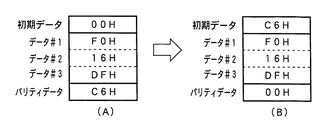
図29は、バックアップパリティデータ作成方法を説明するための説明図である。ただし、図29に示す例では、簡単のために、バックアップデータRAM領域のデータのサイズを3バイトとする。また、図29に示す例では、ステップS484においてチェックサム算出回数として3がセットされる。電源電圧低下にもとづく停電発生処理において、図29(A)に示すように、バックアップチェックデータ領域に、初期データ(この例では00H)が設定される。次に、「00H」とチェックサム算出開始アドレス(この例では「F0H」)の排他的論理和がとられ、その結果と次のポインタが指すRAM領域の内容(本例では「16H」)の排他的論理和がとられる。さらに、その結果と次のポインタが指すRAM領域の内容(本例では「DFH」)の排他的論理和がとられる。そして、その結果(この例では「39H」)を反転したデータ(この例では「C6H」)がバックアップパリティデータ領域に設定される。
【0182】
電源が再投入されたときには、チェックサム確認処理(ステップS9b)においてパリティ診断が行われるが、図29(B)はパリティ診断の例を示す説明図である。バックアップ領域の全データがそのまま保存されていれば、電源再投入時に、図29(A)に示すようなデータがバックアップ領域に設定されている。
【0183】
ステップS51の処理において、CPU56は、バックアップRAM領域のバックアップパリティデータ領域に設定されていたデータ(この例では「C6H」)を初期データとし、初期データを反転したデータ(この例では「39H」)を用いて、バックアップデータ領域の各データについて順次排他的論理和をとる処理を行う。バックアップ領域の全データがそのまま保存されていれば、最終的な演算結果は、「00H」、すなわちバックアップチェックデータ領域に設定されているデータと一致する。バックアップRAM領域内のデータにビット誤りが生じていた場合には、最終的な演算結果は「00H」にならない。
【0184】
よって、CPU56は、パリティチェック処理(チェックサム確認処理)において、最終的な演算結果とバックアップチェックデータ領域に設定されているデータとを比較して、一致すればパリティ診断正常とする。一致しなければ、パリティ診断異常とする。
【0185】
次いで、CPU56は、RAMアクセスレジスタにアクセス禁止値を設定する(ステップS492)。以後、内蔵RAM55のアクセスができなくなる。
【0186】
さらに、CPU56は、クリアデータ(00)を適当なレジスタにセットし(ステップS493)、処理数(この例では「7」)を別のレジスタにセットする(ステップS494)。また、出力ポート0のアドレスをIOポインタに設定する(ステップS495)。IOポインタとして、さらに別のレジスタが用いられる。
【0187】
そして、IOポインタが指すアドレスにクリアデータをセットするとともに(ステップS496)、IOポインタの値を1増やし(ステップS497)、処理数の値を1減算する(ステップS498)。ステップS496〜S498の処理が、処理数の値が0になるまで繰り返される。その結果、全ての出力ポート0〜6(図19および図20参照)にクリアデータが設定される。図19および図20に示すように、この例では、「1」がオン状態であり、クリアデータである「00」が各出力ポートにセットされるので、全ての出力ポートがオフ状態になる。
【0188】
従って、遊技状態を保存するための処理(この例では、チェックサムの生成およびRAMアクセス防止)が実行された後、各出力ポートは直ちにオフ状態になる。なお、この実施の形態では、遊技制御処理において用いられるデータが格納されるRAM領域は全て電源バックアップされている。従って、その内容が正しく保存されているか否かを示すチェックサムの生成処理、およびその内容を書き換えないようにするためのRAMアクセス防止処理が、遊技状態を保存するための処理に相当する。
【0189】
遊技状態を保存するための処理が実行された後、直ちに各出力ポートがオフ状態になるので、保存される遊技状態と整合しない状況が発生することは確実に防止される。図26〜図29に示す処理が実行されるときには、遊技機に対する電源供給が停止するので、電気部品に印加される電圧が低下していく。そして、印加電圧が駆動可能電圧を下回った時点で電気部品の駆動は停止する。従って、遊技機に対する電力供給停止時には、短時間の遅れはあるものの電気部品の駆動は停止する。
【0190】
出力ポートに対するクリア処理が完了すると、CPU56は、待機状態(ループ状態)に入る。従って、システムリセットされるまで、何もしない状態になる。
【0191】
なお、この実施の形態では、NMIに応じて電力供給停止時処理が実行されたが、電源断信号をCPU56のマスク可能端子に接続し、マスク可能割込処理によって電力供給停止時処理を実行してもよい。また、電源断信号を入力ポートに入力し、入力ポートのチェック結果に応じて電力供給停止時処理を実行してもよい。
【0192】
また、この実施の形態では、電源断信号に応じて起動される処理の最初にレジスタの保存処理が行われたが、スイッチ検出処理においてレジスタを使用しない場合には、スイッチ検出処理の実行後に、すなわち、バックアップフラグの設定とチェックサムの算出の処理の前にレジスタ保存処理を行うことができる。その場合には、レジスタ保存処理、バックアップフラグ設定処理、チェックサム算出処理および出力ポートのオフ設定処理を電力供給停止時処理と見なすことができる。さらに、スイッチ検出処理において幾つかのレジスタを使用する場合であっても、使用しないレジスタについては、バックアップフラグの設定とチェックサムの算出の処理の前にレジスタ保存処理を行うことができる。
【0193】
図30は、電力供給停止時の遊技機の動作を説明するためのタイミング図である。(A)に示すように、電源電圧が低下し、VSLの電圧値が電源断信号出力レベル(この例では+22V)まで低下すると電源断信号が発生する。具体的には、電源断信号がローレベルになる。すると、主基板31のCPU56は、電力供給停止時処理の実行を開始し、その処理が終了すると、何の制御もしないループ状態(待機状態)に入る。
【0194】
電源基板910に搭載されているカウンタ971(図9参照)は、電源断信号がローレベルになるとカウントを開始するのであるが、カウントアップ値は、電源断信号がローレベルになってから、VSLの電圧値がVcc生成可能電圧にまで低下する時間以上に設定される。すなわち、少なくとも、電源電圧が、制御動作が不能になる電圧にまで低下する時間以上に設定される。カウンタ971はVccを電源として動作するので、カウントアップ値は、カウンタ971の動作可能期間に相当する値以上に設定される。従って、一般には、カウンタ971がカウントアップして復帰信号が出力される前に、カウンタ971およびその他の回路部品は動作しなくなる。
【0195】
図30(A)に示すように、電源断信号がオン(この例ではハイレベルからローレベルに変化)するあたりで賞球払出が実行された場合、払出検出手段からの検出信号の入力処理が実行される所定期間内で賞球カウントスイッチ301Aがオンする。従って、電源断信号がオンするあたりで実行された球払出についても、電力供給停止時処理が実行される際に、遊技制御手段はバックアップRAMの内容に反映することができる。
【0196】
電源の瞬断等が生ずると、図30(B)に示すように、VSLの電圧レベルが短期間低下した後に復旧する。VSLの電圧レベルが電源断信号出力レベル以下になると、電源断信号がローレベルになって、電力供給停止時処理が開始される。そして、CPU56は電力供給停止時処理終了後にループ状態に入る。何らの制御も行わないと、ループ処理から抜けられないのであるが、この場合には、カウンタ971がカウントアップして復帰信号が発生する。
【0197】
図10に示されたように、主基板31において、復帰信号は、AND回路161介して、CPU56のリセット端子に入力される。従って、CPU56にはシステムリセットがかかる。その結果、CPU56は、待機状態である無限ループの状態から抜け出すことができる。CPU56は、システムリセットが解除されると、すなわち復帰信号がハイレベルになると、電源投入時の場合と同様に、起動時の先頭番地からプログラムを実行する。
【0198】
なお、図30(B)には、カウンタ971のカウントアップ後に、直ちに復帰信号が出力される場合が示されているが、図9に示されたように電源基板910には遅延回路974があるので、主基板31のCPU56に対する復帰信号の供給タイミングは、払出制御用CPU371に対する復帰信号の供給タイミングよりも遅れる。すなわち、通常の電力供給開始時にリセット信号が与えられる場合と同様に、遊技制御手段のリセット解除タイミングは、払出制御手段のリセット解除タイミングに対して遅れる。よって、復帰信号によって制御動作が復旧する場合も、遊技制御手段は、他の電気部品制御手段に対して、遅れて起動されることになる。
【0199】
図31は、払出制御用CPU371周りの一構成例を示すブロック図である。図31に示すように、電源基板910の電源監視回路(電源監視手段)からの電源断信号が、バッファ回路960を介して払出制御用CPU371のマスク不能割込端子(XNMI端子)に接続されている。従って、払出制御用CPU371は、マスク不能割込処理によって電源断の発生を確認することができる。また、電源基板910からのリセット信号と復帰信号とはAND回路385に入力され、AND回路385の出力が払出制御用CPU371のリセット端子に入力される。
【0200】
払出制御用CPU371のCLK/TRG2端子には、主基板31からのINT信号が接続されている。CLK/TRG2端子にクロック信号が入力されると、払出制御用CPU371に内蔵されているタイマカウンタレジスタCLK/TRG2の値がダウンカウントされる。そして、レジスタ値が0になると割込が発生する。従って、タイマカウンタレジスタCLK/TRG2の初期値を「1」に設定しておけば、INT信号の入力に応じて割込が発生することになる。なお、INT信号とは、遊技制御手段から払出制御手段に対する払出制御コマンドが送出されたことを意味する信号である。払出制御用CPU371は、INT信号の入力に応じて発生する割込によって、払出制御コマンド受信処理を開始する。
【0201】
図32は、この実施の形態における出力ポートの割り当てを示す説明図である。図32に示すように、出力ポートC(アドレス00H)は、払出モータ289に出力される駆動信号の出力ポートである。また、出力ポートD(アドレス01H)は、7セグメントLEDであるエラー表示LED374に出力される表示制御信号の出力ポートである。そして、出力ポートE(アドレス02H)は、振分ソレノイド310に出力される駆動信号、およびカードユニット50に対するEXS信号とPRDY信号とを出力するための出力ポートである。
【0202】
図33は、この実施の形態における入力ポートのビット割り当てを示す説明図である。図33に示すように、入力ポートA(アドレス06H)は、主基板31から送出された払出制御コマンドの8ビットの払出制御信号を取り込むための入力ポートである。また、入力ポートB(アドレス07H)のビット0〜2には、それぞれ、賞球カウントスイッチ301A、球貸しカウントスイッチ301B、モータ位置センサの検出信号入力される。ビット3〜6には、カードユニット50からのBRDY信号、BRQ信号、VL信号の出力信号が入力される。
【0203】
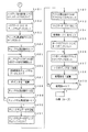
図34は、払出制御用CPU371が実行するメイン処理を示すフローチャートである。遊技機に対して電源が投入され、リセット端子の入力レベルがハイレベルになると、払出制御用CPU371は、ステップS701以降のメイン処理を開始する。なお、リセット端子の入力レベルがハイレベルになる場合として、遊技機に対する電力供給が開始された場合の他に、電源基板910から復帰信号が入力された場合(ローレベルからハイレベルに変化した場合)がある。
【0204】
初期設定処理において、払出制御用CPU371は、割込禁止に設定する(ステップS701)。次に、割込モードを割込モード2に設定し(ステップS702)、スタックポインタにスタックポインタ指定アドレスを設定する(ステップS703)。また、払出制御用CPU371は、内蔵デバイスレジスタの初期化を行い(ステップS704)、CTCおよびPIOの初期化(ステップS705)を行った後に、RAMをアクセス可能状態に設定する(ステップS706)。
【0205】
この実施の形態では、内蔵CTCのうちの一つのチャネルがタイマモードで使用される。従って、ステップS704の内蔵デバイスレジスタの設定処理およびステップS705の処理において、使用するチャネルをタイマモードに設定するためのレジスタ設定、割込発生を許可するためのレジスタ設定および割込ベクタを設定するためのレジスタ設定が行われる。そして、そのチャネルによる割込がタイマ割込として用いられる。タイマ割込を例えば2ms毎に発生させたい場合は、初期値として2msに相当する値が所定のレジスタ(時間定数レジスタ)に設定される。
【0206】
なお、タイマモードに設定されたチャネル(この実施の形態ではチャネル3)に設定される割込ベクタは、タイマ割込処理の先頭番地に相当するものである。具体的は、Iレジスタに設定された値と割込ベクタとでタイマ割込処理の先頭番地が特定される。タイマ割込処理ではタイマ割込フラグがセットされ、メイン処理でタイマ割込フラグがセットされていることが検知されると、払出制御処理が実行される。すなわち、タイマ割込処理では、電気部品制御処理の一例である払出制御処理を実行するための設定がなされる。
【0207】
また、内蔵CTCのうちの他の一つのチャネル(この実施の形態ではチャネル2)が、遊技制御手段からの払出制御コマンド受信のための割込発生用のチャネルとして用いられ、そのチャネルがカウンタモードで使用される。従って、ステップS704の内蔵デバイスレジスタの設定処理およびステップS705の処理において、使用するチャネルをカウンタモードに設定するためのレジスタ設定、割込発生を許可するためのレジスタ設定および割込ベクタを設定するためのレジスタ設定が行われる。
【0208】
カウンタモードに設定されたチャネル(チャネル2)に設定される割込ベクタは、後述するコマンド受信割込処理の先頭番地に相当するものである。具体的は、Iレジスタに設定された値と割込ベクタとでコマンド受信割込処理の先頭番地が特定される。
【0209】
この実施の形態では、払出制御用CPU371でも割込モード2が設定される。従って、内蔵CTCのカウントアップにもとづく割込処理を使用することができる。また、CTCが送出した割込ベクタに応じた割込処理開始番地を設定することができる。
【0210】
CTCのチャネル2(CH2)のカウントアップにもとづく割込は、上述したタイマカウンタレジスタCLK/TRG2の値が「0」になったときに発生する割込である。従って、例えばステップS705において、特定レジスタとしてのタイマカウンタレジスタCLK/TRG2に初期値「1」が設定される。また、CTCのチャネル3(CH3)のカウントアップにもとづく割込は、CPUの内部クロック(システムクロック)をカウントダウンしてレジスタ値が「0」になったら発生する割込であり、後述する2msタイマ割込として用いられる。具体的には、CH3のレジスタ値はシステムクロックの1/256周期で減算される。ステップS705において、CH3のレジスタには、初期値として2msに相当する値が設定される。
【0211】
CTCのCH2のカウントアップにもとづく割込は、CH3のカウントアップにもとづく割込よりも優先順位が高い。従って、同時にカウントアップが生じた場合に、CH2のカウントアップにもとづく割込、すなわち、コマンド受信割込処理の実行契機となる割込の方が優先される。
【0212】
次いで、払出制御用CPU371は、払出制御用のバックアップRAM領域にバックアップデータが存在しているか否かの確認を行う(ステップS708)。例えば、主基板31のCPU56の処理と同様に、電源断時にセットされるバックアップフラグがセット状態になっているか否かによって、バックアップデータが存在しているか否か確認する。バックアップフラグがセット状態になっている場合には、バックアップデータありと判断する。
【0213】
バックアップありを確認したら、払出制御用CPU371は、バックアップRAM領域のデータチェック(この例ではパリティチェック)を行う。不測の電源断が生じた後に復旧した場合には、バックアップRAM領域のデータは保存されていたはずであるから、チェック結果は正常になる。チェック結果が正常でない場合には、内部状態を電源断時の状態に戻すことができないので、停電復旧時でない電源投入時に実行される初期化処理を実行する。
【0214】
チェック結果が正常であれば(ステップS709)、払出制御用CPU371は、内部状態を電源断時の状態に戻すための払出状態復旧処理を行う(ステップS710)。そして、バックアップRAM領域に保存されていたPC(プログラムカウンタ)の指すアドレスに復帰する。
【0215】
初期化処理では、払出制御用CPU371は、まず、RAMクリア処理を行う(ステップS711)。そして、2ms毎に定期的にタイマ割込がかかるように払出制御用CPU371に設けられているCTCのレジスタの設定が行われる(ステップS712)。すなわち、初期値として2msに相当する値が所定のレジスタ(時間定数レジスタ)に設定される。そして、初期設定処理のステップS701において割込禁止とされているので、初期化処理を終える前に割込が許可される(ステップS713)。
【0216】
この実施の形態では、払出制御用CPU371の内蔵CTCが繰り返しタイマ割込を発生するように設定される。この実施の形態では、繰り返し周期は2msに設定される。そして、タイマ割込が発生すると、図35に示すように、払出制御用CPU371は、例えばタイマ割込が発生したことを示すタイマ割込フラグをセットする(ステップS721)。なお、図35には割込を許可することも明示されているが(ステップS720)、2msタイマ割込処理では、最初に割込許可状態に設定される。すなわち、2msタイマ割込処理中には割込許可状態になってので、INT信号の入力にもとづく払出制御コマンド受信処理を優先して実行することができる。
【0217】
払出制御用CPU371は、ステップS724において、タイマ割込フラグがセットされたことを検出するとステップS751以降の払出制御処理を実行する。以上の制御によって、この実施の形態では、払出制御処理は2ms毎に起動されることになる。なお、この実施の形態では、タイマ割込処理ではフラグセットのみがなされ、払出制御処理はメイン処理において実行されるが、タイマ割込処理で払出制御処理を実行してもよい。
【0218】
払出制御処理において、払出制御用CPU371は、まず、中継基板72を介して入力ポート372bに入力される賞球カウントスイッチ301A、球貸しカウントスイッチ301Bがオンしたか否かを判定する(スイッチ処理:ステップS751)。
【0219】
次に、払出制御用CPU371は、センサ(例えば、払出モータ289の回転数を検出するモータ位置センサ)からの信号入力状態を確認してセンサの状態を判定する等の処理を行う(入力判定処理:ステップS752)。払出制御用CPU371は、さらに、受信した払出制御コマンドを解析し、解析結果に応じた処理を実行する(コマンド解析実行処理:ステップS753)。
【0220】
次いで、払出制御用CPU371は、主基板31から払出停止指示コマンドを受信していたら払出停止状態に設定し、払出開始指示コマンドを受信していたら払出停止状態の解除を行う(ステップS754)。また、プリペイドカードユニット制御処理を行う(ステップS755)。
【0221】
次いで、払出制御用CPU371は、球貸し要求に応じて貸し球を払い出す制御を行う(ステップS756)。このとき、払出制御用CPU371は、振分ソレノイド310によって球振分部材311を球貸し側に設定する。
【0222】
さらに、払出制御用CPU371は、総合個数記憶に格納された個数の賞球を払い出す賞球制御処理を行う(ステップS757)。このとき、払出制御用CPU371は、振分ソレノイド310によって球振分部材311を賞球側に設定する。そして、出力ポート372cおよび中継基板72を介して球払出装置97の払出機構部分における払出モータ289に対して駆動信号を出力し、所定の回転数分払出モータ289を回転させる払出モータ制御処理を行う(ステップS758)。
【0223】
なお、この実施の形態では、払出モータ289としてステッピングモータが用いられ、それらを制御するために1−2相励磁方式が用いられる。従って、具体的には、払出モータ制御処理において、8種類の励磁パターンデータが繰り返し払出モータ289に出力される。また、この実施の形態では、各励磁パターンデータが4msずつ出力される。
【0224】
次いで、エラー検出処理が行われ、その結果に応じてエラー表示LED374に所定の表示を行う(エラー処理:ステップS759)。
【0225】
なお、出力ポートCは、払出制御処理における払出モータ制御処理(ステップS758)でアクセスされる。また、出力ポートDは、払出制御処理におけるエラー処理(ステップS759)でアクセスされる。そして、出力ポートEは、払出制御処理における球貸し制御処理(ステップS756)および賞球制御処理(ステップS757)でアクセスされる。
【0226】
図36は、払出制御用CPU371が内蔵するRAMの使用例を示す説明図である。この例では、バックアップRAM領域に、総合個数記憶(例えば2バイト)と貸し球個数記憶とがそれぞれ形成されている。総合個数記憶は、主基板31の側から指示された賞球払出個数の総数を記憶するものである。貸し球個数記憶は、未払出の球貸し個数を記憶するものである。
【0227】
このように、未払出の賞球個数と貸し球個数とが、所定期間はその内容を保持可能なバックアップRAM領域に記憶されるので、停電等の不測の電源断が生じても、所定期間内に電源復旧すれば、バックアップRAM領域に記憶される賞球処理および球貸し処理を続行できる。従って、遊技者に与えられる不利益を低減することができる。
【0228】
図37〜図39は、電源基板910からの電源断信号に応じて実行されるマスク不能割込処理(電力供給停止時処理)の処理例を示すフローチャートである。この例では、NMIに応じて電力供給停止時処理が実行されるが、電源断信号を払出制御用CPU371のマスク可能端子に接続し、マスク可能割込処理によって電力供給停止時処理を実行してもよい。また、電源断信号を入力ポートに入力し、入力ポートのチェック結果に応じて電力供給停止時処理を実行してもよい。
【0229】
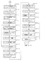
マスク不能割込処理において、払出制御用CPU371は、AFレジスタを所定のバックアップRAM領域に退避する(ステップS801)。また、割込フラグをパリティフラグにコピーする(ステップS802)。パリティフラグはバックアップRAM領域に形成されている。また、BCレジスタ、DEレジスタ、HLレジスタ、IXレジスタおよびスタックポインタをバックアップRAM領域に退避する(ステップS804〜808)。なお、電源復旧時には、退避された内容にもとづいてレジスタ内容が復元され、パリティフラグの内容に応じて、割込許可状態/禁止状態の内部設定がなされる。
【0230】
次いで、払出モータ289に出力される駆動信号をオフ状態にする(ステップS761)。よって、球払出装置97の駆動は停止する。その後、この実施の形態では、所定期間、払出検出手段としての賞球カウントスイッチ301A(賞遊技媒体検出手段に相当)および球貸しカウントスイッチ301B(貸出遊技媒体検出手段に相当)の検出信号をチェックする。そして、賞球カウントスイッチ301Aがオンしたら総合個数記憶の内容を1減らす。また、球貸しカウントスイッチ301Bがオンしたら貸し球個数記憶の内容を1減らす。
【0231】
なお、この実施の形態では、所定期間を計測するために、所定期間計測用カウンタが用いられる。所定期間計測用カウンタの値は、初期値mから、以下に説明するスイッチ検出処理のループ(S763から始まってS763に戻るループ)が1回実行される毎に−1され、その値が0になると、所定期間が終了したとする。検出処理のループでは、例外はあるがほぼ一定の処理が行われるので、ループの1周に要する時間のm倍の時間が、ほぼ所定期間に相当する。
【0232】
所定期間を計測するために、払出制御用CPU371の内蔵タイマを用いてもよい。すなわち、スイッチ検出処理開始時に、内蔵タイマに所定値(所定期間に相当)を設定しておく。そして、スイッチ検出処理のループが1回実行される毎に、内蔵タイマのカウント値をチェックする。そして、カウント値が0になったら、所定期間が終了したとする。内蔵タイマの値が0になったことを検出するために内蔵タイマによる割込を用いることもできるが、この段階では制御内容(RAMに格納されている各値など)を変化させないように、割込を用いず、内蔵タイマのカウント値を読み出してチェックするようなプログラム構成の方が好ましい。また、所定期間は、遊技球が、球払出装置97から落下した時点から、賞球カウントスイッチ301Aまたは球貸しカウントスイッチ301Bに到達するまでの時間以上に設定される。
【0233】
少なくとも、スイッチ検出処理が実行される所定期間では、賞球カウントスイッチ301Aおよび球貸しカウントスイッチ301Bが遊技球を検出できる状態でなければならない。そこで、この実施の形態では、図10に示されたように、電源基板910におけるコンバータIC922の入力側に比較的大容量の補助駆動電源としてのコンデンサ923が接続されている。よって、遊技機に対する電力供給停止時にも、ある程度の期間は+12V電源電圧がスイッチ駆動可能な範囲に維持され、賞球カウントスイッチ301Aおよび球貸しカウントスイッチ301Bが動作可能になる。その期間が、上記の所定期間以上になるように、コンデンサの容量が決定される。
【0234】
なお、入力ポートおよび払出制御用CPU371も、コンバータIC922で作成される+5V電源で駆動されるので、電力供給停止時にも、比較的長い期間動作可能になっている。
【0235】
さらに、この実施の形態では、賞球路と貸し球路とを切り換えるために振分ソレノイド310が用いられている。よって、図10に示されたコンデンサ923の容量は、少なくとも上記の所定期間の間、振分ソレノイド310も駆動できるような容量になっている。なお、コンデンサ923は、VSLの電源ラインと並列接続されているが、電源断信号に応じて遊技制御手段が他のソレノイド(大入賞口開閉用等)の駆動信号をオフ状態にしているので、電源断信号発生後では、コンデンサ923は、各ソレノイドのうちでは振分ソレノイド310のみを駆動できればよい。
【0236】
なお、この実施の形態で用いられているコンデンサ923は補助駆動電源の一つの例であるが、補助駆動電源として他のものを用いてもよい。少なくとも、上記の所定期間の間は、賞球カウントスイッチ301A、球貸しカウントスイッチ301B、振分ソレノイド310および払出制御用CPU371等の払出制御手段を駆動できるものであれば、他の態様の補助駆動電源を用いることができる。
【0237】
払出検出手段からの検出信号の入力処理(スイッチ検出処理)では、払出制御用CPU371は、まず、所定期間計測用カウンタに、所定期間に対応した値mを設定する(ステップS762)。そして、払出制御用CPU371は、所定期間計測用カウンタの値を−1し(ステップS763)、所定期間計測用カウンタの値を確認する(ステップS764)。その値が0であれば、スイッチ検出処理を終了し、制御状態を保存するための処理である電力供給停止時処理に移行する。
【0238】
所定期間計測用カウンタの値が0になっていなければ、賞球カウントスイッチオン中であるか否か確認する(ステップS765)。オン中であれば、検出期間用カウンタの値を1減らした後(ステップS766)、検出期間用カウンタの値が0になったか否か確認する(ステップS767)。0になっていれば、入力ポートを介して賞球カウントスイッチ301Aの検出信号を確認し(ステップS768)、オン状態を示していれば、賞球カウントスイッチ301Aが確実にオンしたとして、総合個数記憶の値を1減らす(ステップS769)。
【0239】
ステップS765で、賞球カウントスイッチオン中でないことを確認したら、入力ポートを介して賞球カウントスイッチ301Aの検出信号を確認し(ステップS770)、オン状態を示していれば、賞球カウントスイッチON中フラグをセットするとともに(ステップS771)、検出期間用カウンタに初期値nをセットする(ステップS772)。
【0240】
以上の処理によって、所定期間内に賞球カウントスイッチ301Aがオンしたら、総合個数記憶の値が−1される。バックアップRAMの内容を保存するための処理は、このようなスイッチ検出処理の後で行われるので、払出が完了した賞球について、必ず総合個数記憶が−1される。従って、遊技球の払出に関して、保存される制御状態に矛盾が生じてしまうことが防止される。また、上記のスイッチ検出処理では、検出期間用カウンタを用いたタイマ処理が施されている。すなわち、一度賞球カウントスイッチ301Aのオンが検出された後、所定時間(S763からS767に至りS763に戻るループにおける処理時間のn倍)の経過後にもオンが検出されないとスイッチオンと見なされない。従って、誤ってスイッチオン検出がなされてしまうことは防止される。
【0241】
なお、通常時のスイッチ処理(図34におけるステップS751)でも、誤検出防止用のタイマ処理が施されている。よって、そのような通常時のスイッチ処理をコールするようにしてもよい。また、ここでは、検出期間用カウンタを用いたタイマ処理が行われたが、所定期間の計測の場合にCPU内蔵タイマを用いてもよいのと同様、CPU内蔵タイマを用いてスイッチ検出処理におけるタイマ処理を実現してもよい。
【0242】
賞球カウントスイッチオン中でなく、かつ、賞球カウントスイッチ301Aのオン状態が検出できない場合には、球貸しカウントスイッチ301Bについてスイッチ検出処理を行う。すなわち、払出制御用CPU371は、球貸しカウントスイッチオン中であるか否か確認する(ステップS775)。オン中であれば、検出期間用カウンタの値を1減らした後(ステップS776)、検出期間用カウンタの値が0になったか否か確認する(ステップS777)。0になっていれば、入力ポートを介して球貸しカウントスイッチ301Bの検出信号を確認し(ステップS778)、オン状態を示していれば、球貸しカウントスイッチ301Bが確実にオンしたとして、貸し球個数記憶の値を1減らす(ステップS779)。
【0243】
ステップS775で、球貸しカウントスイッチオン中でないことを確認したら、入力ポートを介して球貸しカウントスイッチ301Bの検出信号を確認し(ステップS780)、オン状態を示していれば、球貸しカウントスイッチON中フラグをセットするとともに(ステップS781)、検出期間用カウンタに初期値nをセットする(ステップS782)。
【0244】
以上の処理によって、所定期間内に球貸しカウントスイッチ301Bがオンしたら、貸し球個数記憶の値が−1される。バックアップRAMの内容を保存するための処理は、このようなスイッチ検出処理の後で行われるので、払出が完了した貸し球について、必ず貸し球個数記憶が−1される。従って、遊技球の払出に関して、保存される制御状態に矛盾が生じてしまうことが防止される。また、上記のスイッチ検出処理では、検出期間用カウンタを用いたタイマ処理が施されている。すなわち、球貸しカウントスイッチ301Bのオンが所定時間以上継続しないとスイッチオンと見なされない。従って、誤ってスイッチオン検出がなされてしまうことは防止される。
【0245】
所定期間が経過すると(ステップS764)、払出制御用CPU371は、バックアップあり指定値(この例では「55H」)をバックアップフラグにストアする(ステップS809)。バックアップフラグはバックアップRAM領域に形成されている。
【0246】
次いで、主基板31のCPU56の処理と同様の処理を行ってパリティデータを作成しバックアップRAM領域に保存する(ステップS810〜S819)。
【0247】
パリティデータを作成してバックアップRAM領域に保存すると、払出制御用CPU371は、RAMアクセスレジスタにアクセス禁止値を設定する(ステップS820)。以後、内蔵RAMのアクセスができなくなる。
【0248】
さらに、払出制御用CPU371は、クリアデータ(00)を適当なレジスタにセットし(ステップS821)、処理数(この例では「3」)を別のレジスタにセットする(ステップS822)。また、出力ポートCのアドレス(この例では「00H」)をIOポインタに設定する(ステップS823)。IOポインタとして、さらに別のレジスタが用いられる。
【0249】
そして、IOポインタが指すアドレスにクリアデータをセットするとともに(ステップS824)、IOポインタの値を1増やし(ステップS825)、処理数の値を1減算する(ステップS827)。ステップS824〜S826の処理が、処理数の値が0になるまで繰り返される。その結果、全ての出力ポートC〜E(図33参照)にクリアデータが設定される。図32に示すように、この例では、「1」がオン状態であり、クリアデータである「00」が各出力ポートにセットされるので、全ての出力ポートがオフ状態になる。
【0250】
従って、遊技状態を保存するための処理(この例では、チェックサムの生成およびRAMアクセス防止)が実行された後、各出力ポートは直ちにオフ状態になる。なお、この実施の形態では、払出制御処理において用いられるデータが格納されるRAM領域は全て電源バックアップされている。従って、その内容が正しく保存されているか否かを示すチェックサムの生成処理、およびその内容を書き換えないようにするためのRAMアクセス防止処理が、払出制御状態を保存するための処理に相当する。
【0251】
以上のように、この実施の形態では、停電等の発生に応じて電源断信号が出力されたら、まず、球払出装置97の駆動を停止した後、所定期間、払出検出手段からの検出信号の入力処理が実行され、その後、払出制御状態を保存するための処理が行われる。従って、停電発生時に払出途中であった遊技球も、バックアップRAMの保存内容に反映される。
【0252】
すなわち、この実施の形態では、遊技機への電力供給停止時に制御状態をバックアップ記憶手段に保存するように構成した場合に、制御の矛盾等を生じさせないようにすることができる。
【0253】
なお、振分ソレノイド310の出力ポート以外の出力ポートのクリア処理を、スイッチ検出処理の実行前(ステップS761の前)に行ってもよい。電力供給停止時処理の実行中では、払出制御用CPU371やスイッチ類はコンデンサの充電電力等で駆動されることになる。出力ポートのクリア処理をスイッチ検出処理の実行前に行った場合には、コンデンサの充電電力等を電力供給停止時処理のために効率的に使用することができる。
【0254】
出力ポートに対するクリア処理が完了すると、払出制御用CPU371は、待機状態(ループ状態)に入る。従って、システムリセットされるまで、何もしない状態になる。
【0255】
なお、ここでは、賞球カウントスイッチ301Aまたは球貸しカウントスイッチ301Bの検出信号がオン状態を示したらタイマ(検出期間用カウンタ)をセットし、タイマがタイムアップしたときにも検出信号がオン状態を示していたら、スイッチが確実にオンしたと判定したが、主基板31のCPU56と同様に、2msのタイマ(2ms計測用カウンタ)がタイムアップする毎に検出信号の判定を行うように構成してもよい。
【0256】
また、この実施の形態でも、電源断信号に応じて起動される処理の最初にレジスタの保存処理が行われたが、スイッチ検出処理においてレジスタを使用しない場合には、スイッチ検出処理の実行後に、すなわち、バックアップフラグの設定とチェックサムの算出の処理の前にレジスタ保存処理を行うことができる。その場合には、レジスタ保存処理、バックアップフラグ設定処理、チェックサム算出処理および出力ポートのオフ設定処理を電力供給停止時処理と見なすことができる。さらに、スイッチ検出処理において幾つかのレジスタを使用する場合であっても、使用しないレジスタについては、バックアップフラグの設定とチェックサムの算出の処理の前にレジスタ保存処理を行うことができる。
【0257】
なお、払出制御用CPU371についても、電源基板910のリセット信号回路950からシステムリセット信号が供給されているので、主基板31のCPU56の場合と同様に、CPUに対して最初にリセット解除を示すレベルを与えるタイミングを、電源電圧がCPUの動作保証電圧になった時点とすることも保証される。
【0258】
また、図30に示された主基板31におけるタイミングと同様に、電源電圧が低下し、VSLの電圧値が電源断信号出力レベル(この例では+22V)まで低下すると電源断信号が発生する。具体的には、電源断信号がローレベルになる。その状況で、払出制御用CPU371は、電力供給停止時処理の実行を開始し、その処理が終了すると、何の制御もしないループ状態(待機状態)に入る。そして、VSLの電圧レベルが短期間低下した後に復旧したような場合には、電源基板910に搭載されているカウンタ971がカウントアップして復帰信号が発生する。復帰信号は払出制御用CPU371のリセット端子に入力されるので、払出制御用CPU371はループ状態から抜け出すことができる。
【0259】
また、電源断信号がオン(この例ではハイレベルからローレベルに変化)するあたりで賞球払出が実行された場合、払出検出手段からの検出信号の入力処理が実行される所定期間内で賞球カウントスイッチ301Aがオンする。従って、電源断信号がオンするあたりで実行された球払出についても、電力供給停止時処理が実行される際に、払出制御手段はバックアップRAM(総合個数記憶)の内容に反映することができる。
【0260】
そして、図9や図13に示されたように電源基板910には遅延回路960が搭載されているので、電源投入時には、電源基板910から各電気部品制御基板に与えられるリセット信号のうち主基板31に与えられるリセット信号が最後に立ち上がる。従って、遊技制御手段は、他の電気部品制御手段よりも遅く制御可能状態になる。その結果、各電気部品制御手段は遊技制御手段からのコマンドを確実に受信することができる。
【0261】
なお、上記の各実施の形態のパチンコ遊技機1は、始動入賞にもとづいて可変表示部9に可変表示される特別図柄の停止図柄が所定の図柄の組み合わせになると所定の遊技価値が遊技者に付与可能になる第1種パチンコ遊技機であったが、始動入賞にもとづいて開放する電動役物の所定領域への入賞があると所定の遊技価値が遊技者に付与可能になる第2種パチンコ遊技機や、始動入賞にもとづいて可変表示される図柄の停止図柄が所定の図柄の組み合わせになると開放する所定の電動役物への入賞があると所定の権利が発生または継続する第3種パチンコ遊技機であっても、本発明を適用できる。
【0262】
また、パチンコ遊技機に限られず、スロット機等においても、何らかの動作をする電気部品が備えられている場合などには本発明を適用することができる。
【0263】
【発明の効果】
以上のように、本発明によれば、遊技機を、リセット手段が、マイクロコンピュータに供給される電源がマイクロコンピュータが動作可能な電圧レベル以上の電圧レベルとなったことを条件にマイクロコンピュータを起動させるリセット解除信号を出力し、遊技制御用マイクロコンピュータおよび払出制御用マイクロコンピュータが、リセット手段からのリセット解除信号の入力にもとづいて動作可能状態となり、払出制御用マイクロコンピュータが動作可能状態となる時期よりも遅い時期に遊技制御用マイクロコンピュータが動作可能状態となるように構成したので、遊技機の電源投入時に確実にマイクロコンピュータが起動し、払出制御用マイクロコンピュータが遊技制御用マイクロコンピュータからのコマンドを確実に受信することができる効果がある。
【0264】
リセット手段が電源基板に搭載されている場合には、一の基板から各マイクロコンピュータに対してリセット解除信号を供給することができるので、部品数を削減することができる。
【0267】
払出制御用マイクロコンピュータが、電力供給停止時信号が出力された場合に、遊技媒体検出手段による払出手段から払い出された遊技媒体を検出する払出検出処理を所定期間実行した後、制御状態の保存に関わる電力供給停止時処理を行うように構成されている場合には、例えば電力供給停止直前に払出装置が払出を行ったにもかかわらず払い出された遊技媒体が検知されず、保存される残払出数と現実の残払出数とが整合しなくなってしまうようなことは確実に防止される。
【0268】
遊技機への電力供給が停止しても、所定期間において遊技媒体検出手段を駆動可能な電力を供給可能な補助駆動電源を備えている場合には、払出検出処理が行われる所定期間において、払出装置から払い出されている遊技媒体が検出されなくなる事態が生じてしまうことはない。
【0269】
遊技制御用マイクロコンピュータおよび払出制御用マイクロコンピュータが、電力供給停止時処理を行った後に待機状態となり、電力供給停止時信号が出力された後の所定の待機期間経過後に電力供給が停止していない場合に待機状態から復帰させるための復帰信号を遊技制御用マイクロコンピュータおよび払出制御用マイクロコンピュータに向けて出力可能な復帰信号出力手段を備えるように構成されている場合には、復帰信号によってマイクロコンピュータを制御実行状態に復帰させることが可能になり、その結果、ごく短時間で復旧する電源の瞬断等が生じても制御に支障を来すことがない。
【0270】
復帰信号は、マイクロコンピュータのリセット信号入力部に入力される場合には、マイクロコンピュータを制御実行状態にさせるための構成を簡略化することができる。
【0271】
復帰信号出力手段からの復帰信号は払出制御用マイクロコンピュータに出力された後に遊技制御用マイクロコンピュータに出力されるように構成されている場合には、復帰信号による各マイクロコンピュータの復帰順序を適切に設定することができ、例えば、復帰直後に遊技制御用マイクロコンピュータから他のマイクロコンピュータに指令信号を送信するような場合に、容易に、受信側のマイクロコンピュータが指令信号を取りこぼさないように構成することができる。
【図面の簡単な説明】
【図1】 パチンコ遊技機を正面からみた正面図である。
【図2】 パチンコ遊技機の裏面に設けられている各基板を示す説明図である。
【図3】 パチンコ遊技機の機構盤を背面からみた背面図である。
【図4】 機構板に設置されている中間ベースユニット周りの構成を示す正面図である。
【図5】 球払出装置を示す分解斜視図である。
【図6】 遊技制御基板(主基板)の回路構成を示すブロック図である。
【図7】 払出制御基板および球払出装置の構成要素などの賞球に関連する構成要素を示すブロック図である。
【図8】 電源基板の一構成例を示すブロック図である。
【図9】 リセット管理回路の構成例を示すブロック図である。
【図10】 主基板におけるCPU周りの一構成例を示すブロック図である。
【図11】 電源投入時のリセット信号の様子を示すタイミング図である。
【図12】 リセットIC651の出力信号例を示すタイミング図である。
【図13】 リセット管理回路の他の構成例を示すブロック図である。
【図14】 主基板におけるCPUが実行するメイン処理を示すフローチャートである。
【図15】 バックアップフラグと遊技状態復旧処理を実行するか否かとの関係の一例を示す説明図である。
【図16】 チェックサムのチェック例を示すフローチャートである。
【図17】 2msタイマ割込処理を示すフローチャートである。
【図18】 遊技状態復旧処理の一例を示すフローチャートである。
【図19】 出力ポートのビット割り当ての一例を示す説明図である。
【図20】 出力ポートのビット割り当ての一例を示す説明図である。
【図21】 入力ポートのビット割り当ての一例を示す説明図である。
【図22】 RAMにおけるスイッチタイマの形成例を示す説明図である。
【図23】 スイッチ処理の一例を示すフローチャートである。
【図24】 スイッチチェック処理の一例を示すフローチャートである。
【図25】 入力判定値テーブルの構成例を示す説明図である。
【図26】 遊技制御手段におけるマスク不能割込処理を示すフローチャートである。
【図27】 遊技制御手段におけるマスク不能割込処理を示すフローチャートである。
【図28】 遊技制御手段におけるマスク不能割込処理を示すフローチャートである。
【図29】 バックアップパリティデータ作成方法を説明するための説明図である。
【図30】 電力供給停止時の遊技機の動作を説明するためのタイミング図である。
【図31】 払出制御用CPU周りの一構成例を示すブロック図である。
【図32】 出力ポートのビット割り当ての一例を示す説明図である。
【図33】 入力ポートのビット割り当ての一例を示す説明図である。
【図34】 払出制御基板におけるCPUが実行するメイン処理を示すフローチャートである。
【図35】 2msタイマ割込処理を示すフローチャートである。
【図36】 払出制御手段におけるRAMの一構成例を示す説明図である。
【図37】 払出制御手段におけるマスク不能割込処理を示すフローチャートである。
【図38】 払出制御手段におけるマスク不能割込処理を示すフローチャートである。
【図39】 払出制御手段におけるマスク不能割込処理を示すフローチャートである。
【符号の説明】
31 遊技制御基板(主基板)
37 払出制御基板
56 CPU
97 球払出装置
301A 賞球カウントスイッチ
301B 球貸しカウントスイッチ
310 振分ソレノイド
311 振分部材
371 払出制御用CPU
910 電源基板[0001]
BACKGROUND OF THE INVENTION
The present invention relates to a gaming machine such as a pachinko gaming machine, a coin gaming machine, or a slot machine in which a game is performed according to a player's operation, and more particularly, according to a player's operation in a gaming area on a gaming board. The present invention relates to a gaming machine in which a game is performed.
[0002]
[Prior art]
As an example of a gaming machine, a game medium such as a game ball is launched into a game area by a launching device, and when a game medium is won in a prize area such as a prize opening provided in the game area, a predetermined number of prize balls are awarded to the player There are things that will be paid out. Further, a variable display unit capable of changing the display state is provided, and is configured to give a predetermined game value to the player when the display result of the variable display unit becomes a predetermined specific display mode There is.
[0003]
The game value means that the state of the variable winning ball device provided in the gaming area of the gaming machine is advantageous to a player who is easy to win and a right to become advantageous to the player. Or a condition that the conditions for paying out premium game media are easily established.
[0004]
In the first type pachinko gaming machine having a variable display unit that displays a special symbol, the display result of the variable display unit that displays the special symbol is usually a combination of a specific display mode defined in advance. " When the big hit occurs, for example, the big winning opening is opened a predetermined number of times, and the game shifts to a big hit gaming state where the hit ball is easy to win. And in each open period, if there is a prize for a predetermined number (for example, 10) of the big prize opening, the big prize opening is closed. And the number of times the special winning opening is opened is fixed to a predetermined number (for example, 16 rounds). An opening time (for example, 29.5 seconds) is determined for each opening, and even if the number of winnings does not reach a predetermined number, the big winning opening is closed when the opening time elapses. Further, when a predetermined condition (for example, winning in the V zone provided in the big prize opening) is not established at the time when the big prize opening is closed, the big hit gaming state is ended.
[0005]
In addition, among the combinations of display modes other than the “big hit” combination, the display results that are already deterministic or temporary at the stage where some of the display results of the plurality of variable display portions are not yet derived and displayed. A state in which the display mode of the variable display unit in which “” is derived and displayed satisfies a display condition that is a combination of specific display modes is referred to as “reach”. Then, when the display result of the identification information variably displayed on the variable display section does not satisfy the condition of “big hit”, it becomes “disconnected”, and the variable display state ends. A player plays a game while enjoying how to generate a big hit.
[0006]
The game progress in the gaming machine is controlled by game control means such as a microcomputer. The identification information, character image, and background image displayed on the variable display device are controlled by display control means that operates in accordance with display control command data from the game control means. In general, the identification information, character image, and background image displayed on the variable display device are a display control microcomputer and a video display processor that generates image data in accordance with instructions from the microcomputer and transfers the image data to the variable display device side ( VDP), the program capacity of the display control microcomputer is large.
[0007]
Therefore, it is impossible to control identification information and the like displayed on the variable display device by the microcomputer of the game control means having a limited program capacity, and the display control microcomputer (separate from the microcomputer of the game control means) Display control means) is used. Therefore, the game control means for controlling the progress of the game needs to transmit a display control command to the display control means.
[0008]
In such a gaming machine, a speaker is provided on the game board, and various sound effects are emitted from the speaker as the game progresses in order to enhance the gaming effect. In addition, light emitters such as lamps and LEDs are provided on the game board, and these light emitters are turned on and off as the game progresses in order to enhance the gaming effect. Generally, sound control for generating sound effects is performed by game control means for controlling the progress of the game. Further, the lighting / extinguishing control of the light emitter is performed by a game control means for controlling the progress of the game.
[0009]
Also, a player generally borrows game media through a gaming machine. In that case, a gaming medium lending mechanism is provided in the gaming machine. The game medium lending mechanism is often shared with a payout mechanism for paying out a prize ball. Even if the game media lending mechanism and the prize ball payout mechanism are shared or separately provided, both perform the operation of paying out game media, so they are mounted on one payout control board. Controlled by the dispense control means.
[0010]
Since the progress of the game is controlled by the game control means mounted on the main board, the number of winning balls based on the winning is determined by the game control means and transmitted to the payout control board. On the other hand, the rental of game media is irrelevant to the progress of the game, and is generally controlled by the payout control means without going through the game control means. In the following description, the game control means and other control means control various electrical components provided in the gaming machine, so they may be referred to as electrical component control means.
[0011]
[Problems to be solved by the invention]
As described above, in the gaming machine, various game device control means (electrical component control means) are mounted in addition to the game control means. Generally, each control means is constituted by a microcomputer. The microcomputer starts its operation by releasing the reset state after a predetermined reset period after the power is turned on. Usually, the microcomputer has a reset terminal. When a low level is input to the reset terminal, the microcomputer is in a reset state and when a high level is input, the microcomputer is in an operable state. Therefore, a system including a microcomputer is configured such that a low level is input to the reset terminal for a predetermined period after power is turned on, and then a high level is continuously input to the reset terminal.
[0012]
Therefore, in general, the microcomputer starts when the input level of the reset terminal becomes a high level. However, if the control of the voltage level input to the reset terminal is not appropriate, the microcomputer may not start normally. In such a case, a process of turning on the power again after turning off the power of the gaming machine becomes necessary. Also, when the power is turned on, the command may be missed if the other control means is not ready for reception even though the game control means has sent the command.
[0013]
Therefore, an object of the present invention is to provide a gaming machine in which a microcomputer is surely activated when a gaming machine is turned on and each control means can reliably receive a command from the gaming control means.
[0014]
[Means for Solving the Problems]
In the gaming machine according to the present invention, a player performs a predetermined game. Pay out premium game media according to winnings A gaming machine, A game control board with a built-in RAM and a game control microcomputer for controlling the progress of the game, and a prize based on a payout control command with a built-in RAM and output from the game control microcomputer in response to winning The payout control board on which a payout control microcomputer for performing payout processing of game media is mounted, and the memory contents of the game control microcomputer and the payout control microcomputer RAM even when the power supply to the gaming machine is stopped Memory content holding means capable of holding for a predetermined period, and power supply monitoring means for monitoring the state of a predetermined power source used in the gaming machine and outputting a power supply stop signal when the occurrence of power interruption is detected. , On condition that the power supplied to the microcomputer is higher than the voltage level at which the microcomputer can operate. Start the microcomputer Reset solution Distrust Output issue The game control microcomputer and the payout control microcomputer are in an operable state based on the input of the reset release signal from the reset means, and the payout control microcomputer But Operable At a later time than when it becomes The game control microcomputer can be operated. State and The game control microcomputer and the payout control microcomputer execute a power supply stop process for retaining the stored contents of the RAM in response to the input of the power supply stop signal from the power supply monitoring means. A control state recovery process for recovering the control state based on the storage contents of the RAM when the supply is started, and the power source monitoring means is a game control microcomputer for the game control board and a payout control microcomputer for the payout control board. And a power supply stop signal is output from the single power supply monitoring means to the game control microcomputer and the payout control microcomputer. It is characterized by that.
[0015]
It has a power supply board that creates the power supply voltage used in gaming machines, Re The setting means may be configured to be mounted on the power supply board.
[0018]
Payout means for paying out game media And game medium detecting means for detecting the game medium paid out from the payout means; With Discharge control microcomputer However, when the power supply stop signal is output, By game medium detection means After executing the payout detection process for detecting the game medium paid out from the payout means for a predetermined period, the power supply stop process related to the storage of the control state may be performed.
[0019]
Even if the power supply to the gaming machine is stopped, an auxiliary driving power source capable of supplying power capable of driving the game medium detecting means in a predetermined period may be provided.
[0020]
Microcomputer for game control and microcomputer for payout control Is a standby signal after the power supply stop process is performed, and when the power supply is not stopped after a predetermined standby period after the power supply stop signal is output, a return signal for returning from the standby state. The Microcomputer for game control and microcomputer for payout control May be configured to include return signal output means that can output toward
[0021]
Signal from reset means and return signal output means The return signal is input to a reset signal input unit of the microcomputer, for example.
[0022]
From return signal output means Is returned to the payout control microcomputer and then to the game control microcomputer. It may be configured as follows.
[0024]
DETAILED DESCRIPTION OF THE INVENTION
Hereinafter, an embodiment of the present invention will be described with reference to the drawings.
First, the overall configuration of a pachinko gaming machine that is an example of a gaming machine will be described. FIG. 1 is a front view of the
[0025]
As shown in FIG. 1, the
[0026]
Near the center of the
[0027]
An open /
[0028]
The
[0029]
In this example, a prize ball lamp 51 that is lit when there is a remaining number of prize balls is provided in the vicinity of one
[0030]
The
[0031]
The hit ball fired from the hit ball launching device enters the
[0032]
The rotation of the image in the
[0033]
When the combination of images in the
[0034]
Next, each board | substrate arrange | positioned at the back surface of the
As shown in FIG. 2, on the back surface of the
[0035]
On the back side of the gaming machine, there are installed a variable
[0036]
Furthermore, a power supply board 910 on which a power supply circuit for generating DC30V, DC21V, DC12V and DC5V is mounted is provided, and a
[0037]
FIG. 3 is a rear view of the mechanism plate of the
[0038]
The game balls paid out from the
[0039]
A lot of prize balls based on the winnings are paid out, the hitting
[0040]
Next, the configuration of the intermediate base unit installed on the
[0041]
A
[0042]
The ball break switches 187a and 187b are locked by locking pieces 188 at positions where it can be detected that about 27 to 28 game balls are present in the
[0043]
The central portion of the
[0044]
Below the
[0045]
FIG. 5 is an exploded perspective view of the
[0046]
As shown in FIG. 5, the
[0047]
The
[0048]
In addition, below the ball
[0049]
[0050]
A recess is formed at the tip of the
[0051]
In other words, the payout motor position sensor including the
[0052]
When the
[0053]
As shown in FIG. 4, a ball sorting member (switching member) 311 is provided below the
[0054]
In this way, by providing the
[0055]
In this embodiment, a
[0056]
FIG. 6 is a block diagram illustrating an example of a circuit configuration in the
[0057]
Although not shown in FIG. 6, the count switch short-circuit signal is also transmitted to the basic circuit 53 via the switch circuit 58.
[0058]
Further, according to the data given from the basic circuit 53, the jackpot information indicating the occurrence of the jackpot, the effective starting information indicating the number of starting winning balls used for starting the image display of the
[0059]
The basic circuit 53 includes a ROM 54 that stores a game control program and the like, a RAM 55 that is an example of storage means (means for storing variation data) used as a work memory, a CPU 56 that performs a control operation according to the program, and an I / O port. Part 57 is included. In this embodiment, the ROM 54 and RAM 55 are built in the CPU 56. That is, the CPU 56 is a one-chip microcomputer. The one-chip microcomputer only needs to incorporate at least the RAM 55, and the ROM 54 and the I / O port unit 57 may be externally attached or built-in.
[0060]
A ball hitting device for hitting and launching a game ball is driven by a
[0061]
In this embodiment, a reset signal whose low level indicates a reset state, a low active return signal, and a low active power-off signal are also input from the power supply board 910 to the
[0062]
In this embodiment, the lamp control means mounted on the
[0063]
FIG. 7 is a block diagram showing components related to payout, such as components of the
[0064]
The CPU 56 of the
[0065]
Further, the detection signal from the prize
[0066]
When there is a winning, a payout control command indicating the number of winning balls is input to the
[0067]
In the
[0068]
The payout control CPU 371 outputs a ball lending number signal indicating the number of lending balls to the
[0069]
Further, a detection signal from the ball lending
[0070]
The
[0071]
A ball lending switch signal and a return switch signal are given from the
[0072]
When the power of the
[0073]
Then, the payout control CPU 371 of the
[0074]
As described above, all signals from the
[0075]
In this embodiment, a reset signal, a return signal, and a power-off signal are also input from the power supply board 910 to the
[0076]
In this embodiment, the case where the
[0077]
FIG. 8 is a block diagram illustrating a configuration example of the power supply substrate 910. The power supply board 910 is installed independently of the electric component control boards such as the
[0078]
The transformer 911 converts AC voltage from the AC power source into 24V. The AC 24V voltage is output to the
[0079]
However, each connector reaching each electric component control board may be provided on the power supply board 910 to supply each voltage from the power supply board 910 to each board without going through the relay board. Further, although one
[0080]
The + 5V line from the DC-DC converter 913 branches to form a backup + 5V line. A large-capacitance capacitor 916 is connected between the backup + 5V line and the ground level. The capacitor 916 is in a storage state with respect to the backup RAM of the electrical component control board when the power supply to the gaming machine is cut off (a RAM that is backed up, that is, a backup storage means that can be in a storage content holding state even when power supply is stopped). It becomes a backup power supply that supplies power so that it can be maintained. Further, a backflow preventing diode 917 is inserted between the + 5V line and the backup + 5V line. In this embodiment, + 5V for backup is supplied to the
[0081]
A battery that can be charged from a + 5V power supply may be used as the backup power supply. In the case of using a battery, a rechargeable battery is used in which the capacity disappears when a state in which no power is supplied from the +5 V power source continues for a predetermined time.
[0082]
Further, a power supply monitoring IC 902 is mounted on the power supply board 910. The power supply monitoring IC 902 detects the occurrence of power interruption by introducing the VSL voltage and monitoring the VSL voltage. Specifically, when the VSL voltage becomes equal to or lower than a predetermined value (+22 V in this example), a power-off signal is output as a power-off occurs. The power supply voltage to be monitored is preferably higher than the power supply voltage (+5 V in this example) of the circuit element mounted on each electric component control board. In this example, VSL, which is a voltage immediately after being converted from AC to DC, is used. A power-off signal from the power monitoring IC 902 is supplied to the
[0083]
The predetermined value for the power monitoring IC 902 to detect the power-off is lower than the normal voltage, but is a voltage that allows the CPU on each electrical component control board to operate for a while. Further, the power monitoring IC 902 is configured to monitor a voltage that is higher than a voltage for driving a circuit element such as a CPU (+5 V in this example) and immediately after being converted from AC to DC. Therefore, the monitoring range can be expanded for the voltage required by the CPU. Therefore, more precise monitoring can be performed. Furthermore, when VSL (+ 30V) is used as the monitoring voltage, the voltage supplied to the various switches of the gaming machine is + 12V, so that it can be expected to prevent erroneous switch-on detection at the time of instantaneous power interruption. That is, when the voltage of the + 30V power supply is monitored, it is possible to detect a decrease in the level before + 12V created after the creation of + 30V starts to drop.
[0084]
Therefore, when the voltage of the + 12V power supply decreases, the switch output becomes in the on state. However, if the power supply interruption is recognized by monitoring the + 30V power supply voltage that decreases faster than + 12V, the power supply is turned on before the switch output shows the on state. It is possible to enter a state of waiting for recovery and not detect switch output.
[0085]
Further, since the power monitoring IC 902 is mounted on the power supply board 910 that is separate from the electrical component control board, a power-off signal can be supplied from the power monitoring circuit to the plurality of electrical component control boards. Even if there are any number of electrical component control boards that require a power-off signal, it is only necessary to provide one power supply monitoring means. Therefore, even if each electrical component control means on each electrical component control board performs return control described later. The cost of the gaming machine does not increase so much.
[0086]
In the configuration shown in FIG. 8, the detection output (power cut-off signal) of the power monitoring IC 902 is supplied to the respective electric component control boards (for example, the
[0087]
Further, a
[0088]
FIG. 9 is a block diagram illustrating a configuration example of the
[0089]
The reset IC 651 monitors the power supply voltage of VSL, which is the power supply voltage equal to the power supply voltage monitored by the power supply monitoring IC 902, and the voltage value is a predetermined value (from the power supply voltage value at which the power supply monitoring IC 902 outputs a power cut-off signal). (Low value) or less, it becomes low level. Therefore, the CPU 56 and the payout control CPU 371 are subjected to a predetermined power supply stop preparation process in response to the power-off signal from the power-supply monitoring IC 902, and then the system is reset.
[0090]
As shown in FIG. 9, the reset signal from the reset IC 651 is input to the
[0091]
The Q6 output of the
[0092]
For example, the detection voltage of the power monitoring IC 902 serving as the power monitoring means (the voltage that outputs the power-off signal) is set to + 22V, and the detection voltage of the reset IC 651 is set to + 9V. In such a configuration, since the power monitoring unit and the reset IC 651 monitor the voltage of the same power source VSL, the timing at which the power monitoring unit outputs a power-off signal and the low level at which the reset IC 651 is at the reset level. Can be reliably set to a desired predetermined period. The desired predetermined period is a period from when the power supply stop preparation process (power supply stop process) is started in response to the power-off signal from the power supply monitoring means until the process is reliably completed.
[0093]
In this example, the detection condition for the power supply monitoring means to output a detection signal is that the + 30V power supply voltage has dropped to + 22V, and the condition for the reset IC 651 to output a low level that is a reset level is + 30V. The power supply voltage has dropped to + 9V. However, the voltage value used here is an example, and other values may be used.
[0094]
However, although the monitoring range is narrowed, it is also possible to use a + 5V power supply voltage as the monitoring voltage of the power supply monitoring means and the reset IC 651. Even in that case, the detection voltage of the power monitoring circuit is set higher than the detection voltage of the reset IC 651.
[0095]
While power is not supplied from the + 5V power source that is the driving power source for the CPU 56 and the payout control CPU 371 of the
[0096]
FIG. 9 shows a configuration in which a reset signal (low level signal) is given twice to the reset terminal of the CPU of each electrical component control board when the power is turned on, but the rising timing of the reset signal is only once. When using a CPU that reliably releases reset even if not, the circuit elements denoted by
[0097]
In this embodiment, when a reset signal is supplied from the power supply board 910 to the CPU of each electrical component control board, the
[0098]
For example, when the CPU 56 of the
[0099]
Further, the power supply board 910 is equipped with a
[0100]
The output of the buffer circuit 973 becomes a return signal to the
[0101]
FIG. 10 is a block diagram illustrating a configuration example around the CPU 56 in the
[0102]
As shown in FIG. 10, the reset signal and the return signal from the power supply board 910 are input to the AND circuit 161, and the output of the AND circuit 161 is input to the reset terminal (reset signal input unit) of the CPU 56.
[0103]
FIG. 11 is a timing chart showing states of output signals of the ICs in the reset IC 651 and the
[0104]
When the
[0105]
Therefore, when the gaming machine is turned on, a signal is supplied to the reset terminal of the CPU of each electrical component control board that once enters the reset release state (high level) and then enters the reset state (low level) again. Is done. That is, when the power is turned on, the reset terminal of the CPU is given a signal that falls to the reset level again after reaching a level indicating reset release and then becomes a level indicating reset release. As a result, even if the CPU is not activated due to the change from the low level to the high level indicating the first reset release, the CPU can be reliably activated by the second change from the low level to the high level. Therefore, the control is surely started when the gaming machine is turned on.
[0106]
As described above, in this embodiment, in other words, the reset state is released after the state of the CPU is stabilized. Such reset control ensures that the CPU starts after a system reset.
[0107]
Note that the widths of the high level pulse (corresponding to the reset release state) and the low level pulse (corresponding to the reset state) output from the
[0108]
The CPU mounted on the electrical component control board is configured to perform a predetermined start-up process such as a security check before starting the original game control process when the reset state is released and the operation is started. There may be. Then, it is desirable that the end point (falling point) of the high level pulse output from the
[0109]
Furthermore, as shown in FIG. 12, the microcomputer is started by setting the voltage at which the output of the reset IC 651 mounted on the power supply board 910 is at a level indicating that the reset is released to a level higher than the voltage level at which the microcomputer can operate. May be ensured. In the example shown in FIG. 12, when the level of VSL (+ 30V) becomes + 22V, the reset IC 651 sets the output to a level indicating reset release.
[0110]
Further, as shown in FIG. 13, a delay circuit 951 for delaying signals generated by the reset IC 651 and the
[0111]
According to the control as described above, it is also ensured that the timing at which the system reset means first gives the CPU a level indicating reset release is the time when the power supply voltage reaches the CPU operation guarantee voltage. In other words, the system reset means can be configured to give a level indicating reset release on condition that the power supplied to the CPU is at a voltage level equal to or higher than the voltage level at which the CPU can operate. Therefore, even when using a CPU that cannot operate reliably unless a reset level is given more than twice when the power is turned on, the second reset is performed after the power supply voltage reaches the CPU operation guarantee voltage. Given to.
[0112]
Next, the operation of the gaming machine will be described.
FIG. 14 is a flowchart showing main processing executed by the CPU 56 on the
[0113]
In the initial setting process, the CPU 56 first sets the interrupt prohibition (step S1). Next, the interrupt mode is set to interrupt mode 2 (step S2), and a stack pointer designation address is set to the stack pointer (step S3). Then, the built-in device register is initialized (step S4). Further, after initialization (step S5) of CTC (counter / timer) and PIO (parallel input / output port) which are built-in devices (built-in peripheral circuits), the RAM is set in an accessible state (step S6).
[0114]
The CPU 56 used in this embodiment has the following three types of maskable interrupt (INT) modes. When a maskable interrupt occurs, the CPU 56 automatically sets the interrupt disabled state and saves the contents of the program counter in the stack.
[0115]
Interrupt mode 0: The built-in device that has issued the interrupt request sends an RST instruction (1 byte) or a CALL instruction (3 bytes) onto the internal data bus of the CPU. Therefore, the CPU 56 executes the instruction at the address corresponding to the RST instruction or the address specified by the CALL instruction. At reset, the CPU 56 automatically enters interrupt
[0116]
Interrupt mode 1: In this mode, when an interrupt is accepted, the mode always jumps to address 0038 (h).
[0117]
Interrupt mode 2: A mode in which the address synthesized from the value (1 byte) of the specific register (I register) of the CPU 56 and the interrupt vector (1 byte: least significant bit 0) output by the built-in device indicates the interrupt address It is. That is, the interrupt address is an address indicated by 2 bytes in which the upper address is the value of the specific register and the lower address is the interrupt vector. Therefore, an interrupt process can be set at an arbitrary address (although it is skipped). Each built-in device has a function of sending an interrupt vector when making an interrupt request.
[0118]
Therefore, when the interrupt
[0119]
Next, the CPU 56 checks whether or not data protection processing for the backup RAM area (for example, power failure occurrence NMI processing such as addition of parity data) has been performed when the power is turned off (step S8). In this embodiment, when an unexpected power failure occurs, processing for protecting data in the backup RAM area is performed. When such protection processing is performed, it is assumed that there is a backup. When it is confirmed that there is no backup, the CPU 56 executes an initialization process.
[0120]
In this embodiment, whether or not there is backup data in the backup RAM area is confirmed by the state of the backup flag set in the backup RAM area when the power is turned off. In this example, as shown in FIG. 15, if “55H” is set in the backup flag area, it means that there is a backup (ON state), and if a value other than “55H” is set, there is no backup (OFF). State).
[0121]
After confirming that there is a backup, the CPU 56 performs a data check of the backup RAM area (parity check in this example).
[0122]
FIG. 16 is a flowchart illustrating an example of the parity check process in step S9. In the parity check process, the CPU 56 first checks whether the data set in the backup parity data area in the RAM 55 is “00” (step S9a). The backup parity data area will be described in detail later. If the data set in the backup parity data area is not “00”, a parity diagnosis (checksum confirmation) is performed (step S9b). If the result of the checksum confirmation is valid (step S9c), the CPU 56 executes a power failure recovery process described later (step S10). If the result of the checksum confirmation is not valid or if the data set in the backup parity data area is “00”, normal initialization processing is executed (steps S11 to S15). .
[0123]
In the case of recovery after an unexpected power failure, the data in the backup RAM area should have been saved, so the check result is normal. If the check result is not normal, the internal state cannot be returned to the state at the time of power-off, and therefore an initialization process that is executed at the time of power-on not at the time of power failure recovery is executed.
[0124]
If the check result is normal (step S9), the CPU 56 performs a game state restoration process for returning the internal state of the game control means and the control state of the electric component control means such as the display control means to the state when the power is cut off. (Step S10). Then, the saved value of the PC (program counter) stored in the backup RAM area is set in the PC, and the address is restored.
[0125]
In this embodiment, after the presence or absence of backup data is confirmed in step S8, the backup area is checked in step S9 when backup data exists. Conversely, the check result of the backup area is After it is confirmed that the data is normal, the presence / absence of backup data may be confirmed. Further, it may be determined whether or not to execute the power failure recovery processing by confirming either one of the presence / absence of backup data or the check of the backup area.
[0126]
Further, for example, in the parity check (step S9) when determining whether or not to execute the power failure recovery process, that is, when determining whether or not to restore the gaming state, a special process in the stored RAM data If it is confirmed that the gaming machine is in a game standby state (not changing in design, not in big hit game, not in probable change, or without starting prize memory) by flag or the like and starting winning memory data The initialization process may be executed without performing the game state restoration process.
[0127]
As described above, in this embodiment, when power supply is started, initialization processing or game state restoration processing is performed based on the check data (checksum data) stored in the backup RAM area when power supply is stopped. Because it is configured to determine whether or not an unexpected power failure such as a power failure occurs, the necessary data can be saved reliably, and the saved data must be used reliably after the power is restored. Can do.
[0128]
In the normal initialization process (steps S11 to S15), the CPU 56 first performs a RAM clear process (step S11). Also, initial value setting processing is performed for setting initial values in predetermined work areas (for example, a normal symbol determination random number counter, a normal symbol determination buffer, a special symbol left middle right symbol buffer, a payout command storage pointer, etc.). Further, processing for initializing the sub-boards (
[0129]
Then, a CTC register set in the CPU 56 is set so that a timer interrupt is periodically generated every 2 ms (step S14). That is, a value corresponding to 2 ms is set in a predetermined register (time constant register) as an initial value. Since the interruption is prohibited in step S1 of the initial setting process, the interruption is permitted before the initialization process is completed (step S15).
[0130]
In this embodiment, the built-in CTC of the CPU 56 is set to repeatedly generate a timer interrupt. In this embodiment, the repetition period is set to 2 ms. When a timer interrupt occurs, as shown in FIG. 17, the CPU 56 sets a timer interrupt flag indicating that a timer interrupt has occurred, for example (step S12).
[0131]
When the execution of the initialization process (steps S11 to S15) is completed, the main process shifts to a loop process in which it is confirmed whether or not a timer interrupt has occurred (step S17). In the loop, display random number update processing (step S16) is also executed.
[0132]
When the CPU 56 recognizes that a timer interrupt has occurred in step S17, it executes the game control process of steps S21 to S31. In the game control process, the CPU 56 first inputs the states of the switches such as the
[0133]
Next, various abnormality diagnosis processing is performed by the self-diagnosis function provided in the
[0134]
Next, a process of updating each counter indicating each determination random number such as a big hit determination random number used for game control is performed (step S23). The CPU 56 further performs a process of updating a display random number such as a random number that determines the type of stop symbol (step S24).
[0135]
Further, the CPU 56 performs special symbol process processing (step S25). In the special symbol process control, corresponding processing is selected and executed according to a special symbol process flag for controlling the
[0136]
Next, the CPU 56 performs a process of setting a display control command related to the special symbol in a predetermined area of the RAM 55 and sending the display control command (special symbol command control process: step S27). In addition, a display control command related to the normal symbol is set in a predetermined area of the RAM 55, and a process of sending the display control command is performed (normal symbol command control process: step S28).
[0137]
Further, the CPU 56 performs information output processing for outputting data such as jackpot information, start information, probability variation information supplied to the hall management computer, for example (step S29).
[0138]
Further, the CPU 56 issues a drive command to the solenoid circuit 59 when a predetermined condition is established (step S30). The solenoid circuit 59 drives the
[0139]
Then, the CPU 56 executes a prize ball process for setting the number of prize balls based on the detection outputs of the
[0140]
With the above control, in this embodiment, the game control process is started every 2 ms. In this embodiment, in the timer interrupt process, for example, only a flag indicating that an interrupt has occurred is set, and the game control process is executed in the main process, but the game control process is performed in the timer interrupt process. May be executed.
[0141]
In addition, the main process includes a process for determining whether or not to shift to the game control process, and whether or not the CPU 56 should shift to the game control process by the timer interrupt process based on the timer interrupt generated periodically. Since the flag for determining whether or not is set or the like, all of the game control processing is surely executed. In other words, until all the game control processes are executed, it is not determined whether or not to shift to the next game control process, so it is guaranteed that all the processes in the game control process are completed. ing.
[0142]
As described above, in this embodiment, the interrupt
[0143]
Hereinafter, the gaming state restoration process will be described.
FIG. 18 is a flowchart showing an example of the gaming state recovery process shown in step S10 of FIG. In this example, the CPU 56 restores the value stored in the backup RAM to each register (step S131). Then, based on the data stored in the backup RAM, the gaming state at the time of power failure is confirmed and returned. That is, based on the data stored in the backup RAM, the
[0144]
As described above, in the game state restoration process, the state of various electrical components is restored according to the restored internal state, and control is performed on the symbol control board 80, the
[0145]
In this embodiment, when the gaming state is restored to the power-off state, the CPU 56 restores the interrupt permission / prohibition state at the previous power-off, so that the value of the parity flag stored in the backup RAM is restored. Is confirmed (step S135). If the parity flag is off, interrupt permission is set (step S136). However, if the parity flag is in the on state, the gaming state restoration process is terminated as it is (while keeping the interrupt prohibited state set in step S1). The fact that the parity flag is in an ON state means that the interrupt was prohibited at the previous power-off, as will be described later. Therefore, when the parity flag is in the on state, no interrupt is permitted.
[0146]
19 and 20 are explanatory diagrams showing assignment of output ports of the game control means in this embodiment. As shown in FIG. 19, the
[0147]
Further, various information output signals from the
[0148]
FIG. 21 is an explanatory diagram showing bit assignment of input ports in this embodiment. As shown in FIG. 21, the winning
[0149]
Of the
[0150]
Next, a specific example of the switch process (step S21) in the main process will be described. In this embodiment, when the ON state of the detection signal continues for a predetermined time, it is certainly determined that the switch is turned on, and processing corresponding to the switch on is started. A switch timer is used to measure the predetermined time. The switch timer is a 1-byte counter formed in the backup RAM area, and is incremented by 1 every 2 ms when the detection signal indicates an ON state. As shown in FIG. 22, the switch timer is provided by the number N of detection signals. In this embodiment, N = 12. In the RAM, the addresses of the switch timers are arranged in the same order as the bit arrangement order of the input ports (from top to bottom shown in FIG. 21).
[0151]
FIG. 23 is a flowchart illustrating a processing example of the switch processing in step S21 in the game control processing. The switch process is first executed in the game control process as shown in FIG. In the switch process, the CPU 56 first inputs data input to the input port 0 (step S71). Next, “8” is set as the number of processes (step S72), and the address of the switch timer for the winning
[0152]
FIG. 24 is a flowchart showing a switch check processing subroutine. In the switch check processing subroutine, the CPU 56 sets port input data, in this case, input data from the
[0153]
If the value of the carry flag is “1” (step S85), that is, if the detection signal of the winning
[0154]
If the value of the carry flag is “0”, that is, if the detection signal of the winning
[0155]
Thereafter, the CPU 56 adds 1 to the pointer (switch timer address) (step S90) and subtracts 1 from the number of processes (step S91). If the number of processes is not 0, the process returns to step S82. Then, the processes in steps S82 to S92 are repeated.
[0156]
The processes of steps S82 to S92 are repeated for the number of processes, that is, eight times, and during that time, the detection signal of the switch input to the 8 bits of the
[0157]
The CPU 56 inputs the data input to the
[0158]
In the switch check processing subroutine, since the above-described processing is executed, the processing of steps S82 to S92 is repeated for the number of processing, that is, four times, and the detection signal of the switch input to the 4 bits of the
[0159]
In this embodiment, since the game control process is started every 2 ms, the switch process is also executed once every 2 ms. Therefore, the switch timer is incremented by 1 every 2 ms.
[0160]
FIG. 25 is an explanatory diagram of a configuration example of the input determination value table. The input determination value table is a ROM area in which a determination value for determining that the switch has been turned on when it is detected how many times it is continuously turned on is set for each switch. As shown in FIG. 25, the input determination value table includes “2”, “50”, “250”, “30”, “250”, “1” in order from the top, that is, in order from the smallest address value. The judgment value is set.
[0161]
In a routine for confirming that the switch is turned on (for example, the prize ball process in step S31 in the main process), the determination value set at the address determined by the start address and the offset value of the input determination value table, and the start of the switch timer The switch timer value determined by the address and the offset value is compared, and if they match, it is determined that the switch is turned on.
[0162]
26 to 28 are flowcharts showing a processing example of a non-maskable interrupt process (power supply stop process) executed in response to a power-off signal from the power supply board 910.
[0163]
In the power supply stop process, the CPU 56 saves the AF register (accumulator and flag register) in a predetermined backup RAM area (step S451). Further, the interrupt flag is copied to the parity flag (step S452). The parity flag is formed in the backup RAM area. Also, the BC register, DE register, HL register, IX register, and stack pointer are saved in the backup RAM area (steps S454 to S458). When the power is restored, the register contents are restored based on the saved contents, and the interrupt permission / prohibition state is internally set according to the contents of the parity flag.
[0164]
Next, in this embodiment, the detection signal of the prize
[0165]
In this embodiment, a predetermined period measuring counter is used to measure the predetermined period. The value of the counter for measuring the predetermined period is decremented by 1 every time a loop of the switch detection process (a loop starting from S461 and returning to S461) described below is executed once from the initial value m, and the value becomes 0. It is assumed that the predetermined period has ended. Since there is an exception in the detection processing loop, almost constant processing is performed, and therefore, m times the time required for one round of the loop corresponds to a predetermined period.
[0166]
In order to measure the predetermined period, a built-in timer of the CPU 56 may be used. That is, a predetermined value (corresponding to a predetermined period) is set in the built-in timer at the start of the switch detection process. Each time the switch detection processing loop is executed once, the count value of the built-in timer is checked. When the count value reaches 0, it is assumed that the predetermined period has ended. An interrupt by the internal timer can be used to detect that the value of the internal timer has reached 0, but at this stage, the control content (such as each value stored in the RAM) should not be changed. A program configuration is preferred in which the count value of the built-in timer is read and checked instead of using a program.
[0167]
The predetermined period is set to be equal to or longer than the time from when the game ball falls from the
[0168]
At least for a predetermined period during which the switch detection process is executed, the prize
[0169]
Since the input port and the CPU 56 are also driven by the + 5V power source created by the
[0170]
In step S461, an initial value n corresponding to a time of 2 ms is set in the 2 ms measurement counter. Then, until the value of the 2 ms measurement counter becomes 0 (step S462), the value of the 2 ms measurement counter is decremented by 1 (step S463).
[0171]
When the value of the 2 ms measurement counter becomes 0, the input of the detection signal of the prize
[0172]
Then, the switch timer indicated by the pointer (the address of the switch timer is set) is loaded (step S468), and the comparison value is shifted to the right (from the upper bit to the lower bit) (step S469). Data of the
[0173]
If the value of the carry flag is “1” (step S470), that is, if the detection signal of the prize
[0174]
When the value of the switch timer becomes 2 (step S473), 1 is subtracted from the value stored in the total prize ball number storage buffer (step S474), and the value of the prize ball information counter is incremented by 1 (step S475). . If the value of the prize ball information counter is 10 or more (step S476), the value of the prize ball information output counter is incremented by 1 (step S477), and the value of the prize ball information counter is incremented by -10 (step S478).
[0175]
Next, the value of the counter for measuring the predetermined period is decremented by -1 (step S479). If the value is not 0, the process returns to step S461.
[0176]
If the prize
[0177]
In this embodiment, the switch detection process of only the winning
[0178]
When the predetermined period has elapsed (step S480), that is, when the value of the counter for measuring the predetermined period becomes 0, the backup specified value ("55H" in this example) is stored in the backup flag (step S481). The backup flag is formed in the backup RAM area. Next, parity data is created (steps S482 to S491). That is, first, the clear data (00) is set in the checksum data area (step S482), and the checksum calculation start address is set in the pointer (step S483). Also, the number of checksum calculations is set (step S484).
[0179]
Then, an exclusive OR between the contents of the checksum data area and the contents of the RAM area pointed to by the pointer is calculated (step S485). The calculation result is stored in the checksum data area (step S486), the pointer value is incremented by 1 (step S487), and the checksum calculation count value is decremented by 1 (step S488). The processing of steps S485 to S488 is repeated until the value of the checksum calculation count becomes 0 (step S489).
[0180]
When the value of the checksum calculation count becomes 0, the CPU 56 inverts the value of each bit of the contents of the checksum data area (step S490). Then, the inverted data is stored in the checksum data area (step S491). This data becomes parity data to be checked when the power is turned on.
[0181]
FIG. 29 is an explanatory diagram for explaining a backup parity data creation method. However, in the example shown in FIG. 29, the size of the data in the backup data RAM area is 3 bytes for simplicity. In the example shown in FIG. 29, 3 is set as the checksum calculation count in step S484. In the power failure generation process based on the power supply voltage drop, as shown in FIG. 29A, initial data (00H in this example) is set in the backup check data area. Next, the exclusive OR of “00H” and the checksum calculation start address (“F0H” in this example) is taken, and the result and the contents of the RAM area pointed to by the next pointer (“16H” in this example) Exclusive OR is taken. Further, the exclusive OR of the result and the contents of the RAM area pointed to by the next pointer (“DFH” in this example) is taken. Then, data (“C6H” in this example) obtained by inverting the result (“39H” in this example) is set in the backup parity data area.
[0182]
When the power is turned on again, parity diagnosis is performed in the checksum confirmation process (step S9b). FIG. 29B is an explanatory diagram showing an example of parity diagnosis. If all the data in the backup area is stored as it is, data as shown in FIG. 29A is set in the backup area when the power is turned on again.
[0183]
In the processing of step S51, the CPU 56 uses the data set in the backup parity data area of the backup RAM area (in this example, “C6H”) as initial data, and data obtained by inverting the initial data (in this example, “39H”). Are used to sequentially obtain exclusive OR for each data in the backup data area. If all the data in the backup area is stored as it is, the final calculation result matches “00H”, that is, the data set in the backup check data area. If a bit error has occurred in the data in the backup RAM area, the final calculation result is not “00H”.
[0184]
Therefore, the CPU 56 compares the final calculation result with the data set in the backup check data area in the parity check process (check sum confirmation process), and if they match, the parity diagnosis is normal. If they do not match, the parity diagnosis is abnormal.
[0185]
Next, the CPU 56 sets an access prohibition value in the RAM access register (step S492). Thereafter, the built-in RAM 55 cannot be accessed.
[0186]
Further, the CPU 56 sets the clear data (00) in an appropriate register (step S493), and sets the number of processes (in this example, “7”) in another register (step S494). Further, the address of the
[0187]
Then, clear data is set at the address pointed to by the IO pointer (step S496), the value of the IO pointer is incremented by 1 (step S497), and the value of the processing number is decremented by 1 (step S498). The processes in steps S496 to S498 are repeated until the value of the number of processes becomes zero. As a result, clear data is set to all the
[0188]
Therefore, after the processing for saving the game state (in this example, checksum generation and RAM access prevention) is executed, each output port is immediately turned off. In this embodiment, the RAM area in which data used in the game control process is stored is all backed up. Therefore, the checksum generation process indicating whether or not the contents are correctly stored and the RAM access prevention process for preventing the contents from being rewritten correspond to the process for storing the gaming state.
[0189]
Since each output port is turned off immediately after the processing for saving the gaming state is executed, it is reliably prevented that a situation that does not match the saved gaming state occurs. When the processes shown in FIGS. 26 to 29 are executed, the power supply to the gaming machine is stopped, so that the voltage applied to the electric component is lowered. When the applied voltage falls below the drivable voltage, the driving of the electrical component is stopped. Therefore, when the power supply to the gaming machine is stopped, the driving of the electrical components is stopped although there is a short delay.
[0190]
When the clear process for the output port is completed, the CPU 56 enters a standby state (loop state). Therefore, nothing is done until the system is reset.
[0191]
In this embodiment, the power supply stop process is executed according to the NMI. However, the power supply stop signal is connected to the maskable terminal of the CPU 56 and the power supply stop process is executed by the maskable interrupt process. May be. Alternatively, a power-off signal may be input to the input port and the power supply stop process may be executed according to the input port check result.
[0192]
Further, in this embodiment, the register saving process is performed at the beginning of the process activated in response to the power-off signal, but when the register is not used in the switch detection process, after executing the switch detection process, That is, the register saving process can be performed before the backup flag setting and the checksum calculation process. In this case, the register saving process, the backup flag setting process, the checksum calculation process, and the output port off setting process can be regarded as a power supply stop process. Further, even when several registers are used in the switch detection process, the register storage process can be performed before the backup flag setting process and the checksum calculation process for the unused registers.
[0193]
FIG. 30 is a timing chart for explaining the operation of the gaming machine when power supply is stopped. As shown in (A), when the power supply voltage is lowered and the voltage value of VSL is lowered to the power-off signal output level (+22 V in this example), a power-off signal is generated. Specifically, the power-off signal becomes low level. Then, the CPU 56 of the
[0194]
The counter 971 (see FIG. 9) mounted on the power supply board 910 starts counting when the power-off signal becomes low level, but the count-up value becomes VSL after the power-off signal becomes low level. Is set to be equal to or longer than the time required for the voltage value to fall to a voltage capable of generating Vcc. That is, at least the power supply voltage is set to be equal to or longer than the time during which the power supply voltage is reduced to a voltage at which the control operation is disabled. Since the
[0195]
As shown in FIG. 30A, when a prize ball payout is executed when the power-off signal is turned on (in this example, it changes from a high level to a low level), detection signal input processing from the payout detection means is performed. The prize
[0196]
When an instantaneous power interruption or the like occurs, as shown in FIG. 30B, the voltage level of VSL is restored after a short period of time drop. When the voltage level of VSL becomes equal to or lower than the power-off signal output level, the power-off signal becomes low level, and the power supply stop process is started. Then, the CPU 56 enters a loop state after the end of the power supply stop process. If no control is performed, the loop process cannot be exited. In this case, the
[0197]
As shown in FIG. 10, in the
[0198]
Note that FIG. 30B shows a case where a return signal is output immediately after the
[0199]
FIG. 31 is a block diagram illustrating a configuration example around the payout control CPU 371. As shown in FIG. 31, the power-off signal from the power supply monitoring circuit (power supply monitoring means) of the power supply board 910 is connected to the non-maskable interrupt terminal (XNMI terminal) of the payout control CPU 371 via the
[0200]
The INT signal from the
[0201]
FIG. 32 is an explanatory diagram showing assignment of output ports in this embodiment. As shown in FIG. 32, the output port C (
[0202]
FIG. 33 is an explanatory diagram showing bit assignment of input ports in this embodiment. As shown in FIG. 33, the input port A (
[0203]
FIG. 34 is a flowchart showing main processing executed by the payout control CPU 371. When power is turned on to the gaming machine and the input level of the reset terminal becomes high level, the payout control CPU 371 starts the main processing after step S701. In addition, as a case where the input level of the reset terminal becomes a high level, in addition to a case where power supply to the gaming machine is started, a case where a return signal is input from the power supply board 910 (a case where the level changes from low level to high level) )
[0204]
In the initial setting process, the payout control CPU 371 sets the interrupt prohibition (step S701). Next, the interrupt mode is set to interrupt mode 2 (step S702), and a stack pointer designation address is set to the stack pointer (step S703). The payout control CPU 371 initializes the built-in device register (step S704), initializes the CTC and PIO (step S705), and then sets the RAM in an accessible state (step S706).
[0205]
In this embodiment, one channel of the built-in CTC is used in the timer mode. Accordingly, in the built-in device register setting process in step S704 and the process in step S705, register setting for setting the channel to be used to timer mode, register setting for permitting interrupt generation, and setting an interrupt vector. The register is set. The interrupt by the channel is used as a timer interrupt. For example, when it is desired to generate a timer interrupt every 2 ms, a value corresponding to 2 ms is set as an initial value in a predetermined register (time constant register).
[0206]
The interrupt vector set for the channel set to the timer mode (
[0207]
Further, another channel (
[0208]
The interrupt vector set in the channel (channel 2) set in the counter mode corresponds to the head address of the command reception interrupt process described later. Specifically, the start address of the command reception interrupt process is specified by the value set in the I register and the interrupt vector.
[0209]
In this embodiment, the
[0210]
The interrupt based on the count-up of the CTC channel 2 (CH2) is an interrupt that occurs when the value of the timer counter register CLK / TRG2 described above becomes “0”. Therefore, for example, in step S705, the initial value “1” is set in the timer counter register CLK / TRG2 as the specific register. An interrupt based on the count-up of CTC channel 3 (CH3) is an interrupt that occurs when the internal clock (system clock) of the CPU is counted down and the register value becomes “0”. Used as an interrupt. Specifically, the register value of CH3 is subtracted at 1/256 period of the system clock. In step S705, the CH3 register is set to a value corresponding to 2 ms as an initial value.
[0211]
Interrupts based on CTC CH2 count-up have a higher priority than interrupts based on CH3 count-up. Therefore, when the count-up occurs simultaneously, the interrupt based on the CH2 count-up, that is, the interrupt that triggers the execution of the command reception interrupt process is given priority.
[0212]
Next, the payout control CPU 371 checks whether backup data exists in the payout control backup RAM area (step S708). For example, as with the processing of the CPU 56 of the
[0213]
After confirming that there is a backup, the payout control CPU 371 performs a data check (parity check in this example) in the backup RAM area. In the case of recovery after an unexpected power failure, the data in the backup RAM area should have been saved, so the check result is normal. If the check result is not normal, the internal state cannot be returned to the state at the time of power-off, and therefore an initialization process that is executed at the time of power-on not at the time of power failure recovery is executed.
[0214]
If the check result is normal (step S709), the payout control CPU 371 performs a payout state recovery process for returning the internal state to the state when the power is turned off (step S710). Then, it returns to the address indicated by the PC (program counter) stored in the backup RAM area.
[0215]
In the initialization process, the payout control CPU 371 first performs a RAM clear process (step S711). Then, the CTC register provided in the payout control CPU 371 is set so that a timer interrupt is periodically generated every 2 ms (step S712). That is, a value corresponding to 2 ms is set in a predetermined register (time constant register) as an initial value. Since the interruption is prohibited in step S701 of the initial setting process, the interruption is permitted before the initialization process is finished (step S713).
[0216]
In this embodiment, the built-in CTC of the payout control CPU 371 is set to repeatedly generate a timer interrupt. In this embodiment, the repetition period is set to 2 ms. When a timer interrupt occurs, as shown in FIG. 35, the payout control CPU 371 sets a timer interrupt flag indicating that a timer interrupt has occurred, for example (step S721). In FIG. 35, it is also clearly indicated that the interrupt is permitted (step S720). In the 2 ms timer interrupt process, the interrupt permission state is first set. In other words, since the interrupt is permitted during the 2 ms timer interrupt process, the payout control command receiving process based on the input of the INT signal can be preferentially executed.
[0217]
The payout control CPU 371 executes a payout control process after step S751 when detecting that the timer interrupt flag is set in step S724. With the above control, in this embodiment, the payout control process is started every 2 ms. In this embodiment, only the flag is set in the timer interrupt process, and the payout control process is executed in the main process, but the payout control process may be executed in the timer interrupt process.
[0218]
In the payout control process, the payout control CPU 371 first determines whether or not the prize
[0219]
Next, the payout control CPU 371 performs processing such as checking the signal input state from a sensor (for example, a motor position sensor that detects the rotation speed of the payout motor 289) and determining the state of the sensor (input determination processing). : Step S752). The payout control CPU 371 further analyzes the received payout control command and executes a process according to the analysis result (command analysis execution process: step S753).
[0220]
Next, the payout control CPU 371 sets the payout stop state if the payout stop instruction command is received from the
[0221]
Next, the payout control CPU 371 performs control for paying out the rental balls in response to the ball rental request (step S756). At this time, the payout control CPU 371 sets the
[0222]
Further, the payout control CPU 371 performs prize ball control processing for paying out the number of prize balls stored in the total number memory (step S757). At this time, the payout control CPU 371 sets the
[0223]
In this embodiment, a stepping motor is used as the
[0224]
Next, error detection processing is performed, and predetermined display is performed on the
[0225]
The output port C is accessed in the payout motor control process (step S758) in the payout control process. The output port D is accessed by error processing (step S759) in the payout control processing. The output port E is accessed in the ball lending control process (step S756) and the prize ball control process (step S757) in the payout control process.
[0226]
FIG. 36 is an explanatory diagram showing a usage example of the RAM built in the payout control CPU 371. In this example, a total number storage (for example, 2 bytes) and a lending ball number storage are formed in the backup RAM area. The total number storage stores the total number of prize balls paid out instructed from the
[0227]
As described above, the number of unpaid prize balls and the number of rented balls are stored in the backup RAM area capable of holding the contents for a predetermined period. Therefore, even if an unexpected power failure such as a power failure occurs, If the power is restored, the winning ball processing and ball lending processing stored in the backup RAM area can be continued. Therefore, the disadvantage given to the player can be reduced.
[0228]
37 to 39 are flowcharts showing a processing example of the non-maskable interrupt processing (power supply stop processing) executed in response to the power-off signal from the power supply board 910. In this example, the power supply stop process is executed according to the NMI, but the power cut signal is connected to the maskable terminal of the payout control CPU 371 and the power supply stop process is executed by the maskable interrupt process. Also good. Alternatively, a power-off signal may be input to the input port and the power supply stop process may be executed according to the input port check result.
[0229]
In the non-maskable interrupt process, the payout control CPU 371 saves the AF register in a predetermined backup RAM area (step S801). Further, the interrupt flag is copied to the parity flag (step S802). The parity flag is formed in the backup RAM area. Also, the BC register, DE register, HL register, IX register, and stack pointer are saved in the backup RAM area (steps S804 to S808). When the power is restored, the register contents are restored based on the saved contents, and the interrupt permission / prohibition state is internally set according to the contents of the parity flag.
[0230]
Next, the drive signal output to the dispensing
[0231]
In this embodiment, a predetermined period measuring counter is used to measure the predetermined period. The value of the counter for measuring the predetermined period is decremented by 1 every time a switch detection processing loop (a loop starting from S763 and returning to S763) described below is executed once from the initial value m. It is assumed that the predetermined period has ended. Since there is an exception in the detection processing loop, almost constant processing is performed, and therefore, m times the time required for one round of the loop corresponds to a predetermined period.
[0232]
In order to measure the predetermined period, an internal timer of the payout control CPU 371 may be used. That is, a predetermined value (corresponding to a predetermined period) is set in the built-in timer at the start of the switch detection process. Each time the switch detection processing loop is executed once, the count value of the built-in timer is checked. When the count value reaches 0, it is assumed that the predetermined period has ended. An interrupt by the internal timer can be used to detect that the value of the internal timer has reached 0, but at this stage, the control content (such as each value stored in the RAM) should not be changed. A program configuration is preferred in which the count value of the built-in timer is read and checked instead of using a program. Further, the predetermined period is set to be equal to or longer than the time from when the game ball falls from the
[0233]
At least in a predetermined period during which the switch detection process is executed, the prize
[0234]
Since the input port and the payout control CPU 371 are also driven by the + 5V power source created by the
[0235]
Furthermore, in this embodiment, the sorting
[0236]
Note that the capacitor 923 used in this embodiment is an example of an auxiliary driving power supply, but another auxiliary driving power supply may be used. At least during the above-mentioned predetermined period, as long as the payout control means such as the prize
[0237]
In the detection signal input process (switch detection process) from the payout detection means, the payout control CPU 371 first sets a value m corresponding to the predetermined period in the predetermined period measurement counter (step S762). Then, the payout control CPU 371 decrements the value of the predetermined period measurement counter by 1 (step S763), and checks the value of the predetermined period measurement counter (step S764). If the value is 0, the switch detection process is terminated, and the process proceeds to a power supply stop process, which is a process for storing the control state.
[0238]
If the value of the counter for measuring the predetermined period is not 0, it is confirmed whether or not the prize ball count switch is on (step S765). If it is ON, the value of the detection period counter is decremented by 1 (step S766), and then it is confirmed whether or not the value of the detection period counter is 0 (step S767). If it is 0, the detection signal of the prize
[0239]
If it is confirmed in step S765 that the prize ball count switch is not on, the detection signal of the prize
[0240]
If the prize
[0241]
Note that a timer process for preventing erroneous detection is also performed in the normal switch process (step S751 in FIG. 34). Therefore, such normal switch processing may be called. Here, the timer process using the counter for the detection period is performed, but the timer in the switch detection process using the CPU built-in timer is the same as in the case of measuring the predetermined period. Processing may be realized.
[0242]
When the winning ball count switch is not on and the ON state of the winning
[0243]
If it is confirmed in step S775 that the ball lending count switch is not on, the detection signal of the ball lending
[0244]
If the ball lending
[0245]
When the predetermined period has elapsed (step S764), the payout control CPU 371 stores the backup specified value ("55H" in this example) in the backup flag (step S809). The backup flag is formed in the backup RAM area.
[0246]
Next, processing similar to that of the CPU 56 of the
[0247]
When the parity data is created and stored in the backup RAM area, the payout control CPU 371 sets an access prohibition value in the RAM access register (step S820). Thereafter, the built-in RAM cannot be accessed.
[0248]
Further, the payout control CPU 371 sets clear data (00) in an appropriate register (step S821), and sets the number of processes (in this example, “3”) in another register (step S822). Further, the address of the output port C (“00H” in this example) is set in the IO pointer (step S823). Another register is used as the IO pointer.
[0249]
Then, clear data is set at the address pointed to by the IO pointer (step S824), the value of the IO pointer is incremented by 1 (step S825), and the value of the processing number is subtracted by 1 (step S827). The processes in steps S824 to S826 are repeated until the value of the number of processes becomes zero. As a result, clear data is set in all the output ports C to E (see FIG. 33). As shown in FIG. 32, in this example, “1” is in the on state and “00” that is the clear data is set in each output port, so that all the output ports are in the off state.
[0250]
Therefore, after the processing for saving the game state (in this example, checksum generation and RAM access prevention) is executed, each output port is immediately turned off. In this embodiment, all RAM areas in which data used in the payout control process are stored are backed up. Therefore, the checksum generation process indicating whether or not the contents are correctly stored and the RAM access prevention process for preventing the contents from being rewritten correspond to the process for storing the payout control state.
[0251]
As described above, in this embodiment, when a power-off signal is output in response to the occurrence of a power failure or the like, first, the driving of the
[0252]
In other words, in this embodiment, when the control state is stored in the backup storage means when the power supply to the gaming machine is stopped, it is possible to prevent a control contradiction or the like from occurring.
[0253]
Note that clearing of output ports other than the output port of the sorting
[0254]
When the clear process for the output port is completed, the payout control CPU 371 enters a standby state (loop state). Therefore, nothing is done until the system is reset.
[0255]
Here, a timer (detection period counter) is set when the detection signal of the winning
[0256]
Also in this embodiment, the register saving process was performed at the beginning of the process activated in response to the power-off signal, but when the register is not used in the switch detection process, after executing the switch detection process, That is, the register saving process can be performed before the backup flag setting and the checksum calculation process. In this case, the register saving process, the backup flag setting process, the checksum calculation process, and the output port off setting process can be regarded as a power supply stop process. Further, even when several registers are used in the switch detection process, the register storage process can be performed before the backup flag setting process and the checksum calculation process for the unused registers.
[0257]
Since the system reset signal is also supplied to the payout control CPU 371 from the
[0258]
Similarly to the timing in the
[0259]
In addition, when a prize ball payout is executed when the power-off signal is turned on (in this example, from a high level to a low level), a prize is received within a predetermined period during which the detection signal input processing from the payout detection means is executed. The
[0260]
Since the
[0261]
The
[0262]
In addition, the present invention is not limited to pachinko gaming machines and can be applied to slot machines and the like when electrical components that perform some kind of operation are provided.
[0263]
【The invention's effect】
As described above, according to the present invention, a gaming machine is Re The setting means is on condition that the power supplied to the microcomputer is at a voltage level higher than the voltage level at which the microcomputer can operate. Start the microcomputer Reset solution Distrust Output The game control microcomputer and the payout control microcomputer become operable based on the input of the reset release signal from the reset means, and the payout control microcomputer But Operable At a later time than when it becomes The game control microcomputer can be operated. Since it is configured to be in a state, the microcomputer is surely activated when the gaming machine is turned on, Discharge control microcomputer Is game control Microcomputer There is an effect that the command from can be received reliably.
[0264]
Re When the setting means is mounted on the power supply board, Microcomputer Reset against Cancel Since a signal can be supplied, the number of parts can be reduced.
[0267]
Discharge control microcomputer However, when the power supply stop signal is output, By game medium detection means In the case where the power supply stop processing related to storage of the control state is performed after a predetermined period of time, the payout detection processing for detecting the game medium paid out from the payout means is performed, for example, immediately before the power supply is stopped. In this case, the paid-out game medium is not detected even though the payout device has paid out, and the stored payout number and the actual remaining payout number are no longer matched. The
[0268]
Even if the power supply to the gaming machine is stopped, if an auxiliary drive power source capable of supplying power capable of driving the game medium detecting means in a predetermined period is provided, the payout is performed in the predetermined period during which the payout detection process is performed. There will be no situation where the game medium paid out from the device is not detected.
[0269]
Microcomputer for game control and microcomputer for payout control Is a standby signal after the power supply stop process is performed, and when the power supply is not stopped after a predetermined standby period after the power supply stop signal is output, a return signal for returning from the standby state. The Microcomputer for game control and microcomputer for payout control In the case where it is configured to include a return signal output means that can output toward the Microcomputer Can be restored to the control execution state, and as a result, even if a power interruption that recovers in a very short time occurs, the control is not hindered.
[0270]
When the return signal is input to the reset signal input section of the microcomputer, Microcomputer Can be simplified in the control execution state.
[0271]
From return signal output means Is returned to the payout control microcomputer and then to the game control microcomputer. If configured, each return signal Microcomputer Return order can be set appropriately, for example, game control immediately after return Microcomputer From other Microcomputer When sending a command signal to the Microcomputer Can be configured not to miss the command signal.
[Brief description of the drawings]
FIG. 1 is a front view of a pachinko gaming machine as viewed from the front.
FIG. 2 is an explanatory view showing each board provided on the back surface of the pachinko gaming machine.
FIG. 3 is a rear view of the mechanism board of the pachinko gaming machine as viewed from the back.
FIG. 4 is a front view showing a configuration around an intermediate base unit installed on a mechanism plate.
FIG. 5 is an exploded perspective view showing a ball dispensing device.
FIG. 6 is a block diagram showing a circuit configuration of a game control board (main board).
FIG. 7 is a block diagram showing components related to a prize ball such as components of a payout control board and a ball payout device.
FIG. 8 is a block diagram illustrating a configuration example of a power supply board.
FIG. 9 is a block diagram illustrating a configuration example of a reset management circuit.
FIG. 10 is a block diagram illustrating an example of a configuration around a CPU in a main board.
FIG. 11 is a timing chart showing a state of a reset signal when power is turned on.
FIG. 12 is a timing chart showing an example of an output signal of the reset IC 651.
FIG. 13 is a block diagram showing another configuration example of the reset management circuit.
FIG. 14 is a flowchart showing main processing executed by the CPU on the main board.
FIG. 15 is an explanatory diagram showing an example of a relationship between a backup flag and whether or not to execute a game state recovery process.
FIG. 16 is a flowchart illustrating a checksum check example;
FIG. 17 is a flowchart showing a 2 ms timer interrupt process.
FIG. 18 is a flowchart showing an example of a game state recovery process.
FIG. 19 is an explanatory diagram illustrating an example of bit assignment of an output port.
FIG. 20 is an explanatory diagram illustrating an example of bit assignment of an output port.
FIG. 21 is an explanatory diagram illustrating an example of bit assignment of an input port.
FIG. 22 is an explanatory diagram showing an example of forming a switch timer in a RAM.
FIG. 23 is a flowchart illustrating an example of switch processing.
FIG. 24 is a flowchart illustrating an example of a switch check process.
FIG. 25 is an explanatory diagram of a configuration example of an input determination value table.
FIG. 26 is a flowchart showing a non-maskable interrupt process in the game control means.
FIG. 27 is a flowchart showing a non-maskable interrupt process in the game control means.
FIG. 28 is a flowchart showing a non-maskable interrupt process in the game control means.
FIG. 29 is an explanatory diagram for explaining a backup parity data creation method;
FIG. 30 is a timing chart for explaining the operation of the gaming machine when power supply is stopped.
FIG. 31 is a block diagram illustrating a configuration example around a payout control CPU;
FIG. 32 is an explanatory diagram illustrating an example of bit assignment of an output port.
FIG. 33 is an explanatory diagram showing an example of bit assignment of an input port.
FIG. 34 is a flowchart showing main processing executed by the CPU in the payout control board.
FIG. 35 is a flowchart showing a 2 ms timer interrupt process.
FIG. 36 is an explanatory diagram showing a configuration example of a RAM in the payout control unit.
FIG. 37 is a flowchart showing a non-maskable interrupt process in the payout control means.
FIG. 38 is a flowchart showing a non-maskable interrupt process in the payout control means.
FIG. 39 is a flowchart showing a non-maskable interrupt process in the payout control means.
[Explanation of symbols]
31 Game control board (main board)
37 Dispensing control board
56 CPU
97 Ball dispenser
301A Prize ball count switch
301B Ball rental count switch
310 Sorting solenoid
311 Sorting member
371 CPU for payout control
910 Power supply board
Claims (7)
RAMを内蔵し、遊技の進行を制御する遊技制御用マイクロコンピュータが搭載された遊技制御基板と、
RAMを内蔵し、入賞に応じて前記遊技制御用マイクロコンピュータから出力される払出制御コマンドにもとづいて景品遊技媒体の払出処理を行う払出制御用マイクロコンピュータが搭載された払出制御基板と、
遊技機への電力供給が停止していても前記遊技制御用マイクロコンピュータおよび前記払出制御用マイクロコンピュータのRAMの記憶内容を所定期間保持させることが可能な記憶内容保持手段と、
遊技機で使用される所定の電源の状態を監視して電源断の発生を検出したときに電力供給停止時信号を出力する電源監視手段と、
前記マイクロコンピュータに供給される電源がマイクロコンピュータが動作可能な電圧レベル以上の電圧レベルとなったことを条件に前記マイクロコンピュータを起動させるリセット解除信号を出力するリセット手段とを備え、
前記遊技制御用マイクロコンピュータおよび前記払出制御用マイクロコンピュータは、前記リセット手段からのリセット解除信号の入力にもとづいて動作可能状態となり、
前記払出制御用マイクロコンピュータが動作可能状態となる時期よりも遅い時期に前記遊技制御用マイクロコンピュータが動作可能状態となり、
前記遊技制御用マイクロコンピュータおよび前記払出制御用マイクロコンピュータは、前記電源監視手段からの電力供給停止時信号の入力に応じて、前記RAMの記憶内容を保持させるための電力供給停止時処理を実行し、電力供給が開始されたときに前記RAMの記憶内容にもとづいて制御状態を復旧させる制御状態復旧処理を実行し、
前記電源監視手段は前記遊技制御基板の前記遊技制御用マイクロコンピュータと前記払出制御基板の前記払出制御用マイクロコンピュータとに接続され、単一の前記電源監視手段から前記遊技制御用マイクロコンピュータと前記払出制御用マイクロコンピュータとに電力供給停止時信号が出力される
ことを特徴とする遊技機。Player have rows predetermined game, a gaming machine pays out a prize game medium according to the winning,
A game control board with a built-in RAM and a game control microcomputer for controlling the progress of the game;
A payout control board having a built-in RAM and mounted with a payout control microcomputer that performs payout processing of prize game media based on payout control commands output from the game control microcomputer in accordance with a prize;
Memory content holding means capable of holding the memory content of the RAM of the gaming control microcomputer and the payout control microcomputer for a predetermined period even when power supply to the gaming machine is stopped;
Power supply monitoring means for monitoring the state of a predetermined power supply used in the gaming machine and outputting a power supply stop signal when the occurrence of a power interruption is detected;
And a reset means power supplied before Symbol microcomputer outputs a reset solutions No. Joshin for activating the microcomputer on the condition that the microcomputer becomes operable voltage level above the voltage level,
The game control microcomputer and the payout control microcomputer are in an operable state based on an input of a reset release signal from the reset means,
Wherein Ri said gaming control microcomputer to the payout control microcomputer timing later than timing at which an operable state Do operable state,
The game control microcomputer and the payout control microcomputer execute a power supply stop process for holding the stored contents of the RAM in response to an input of a power supply stop signal from the power supply monitoring means. Executing a control state recovery process for recovering the control state based on the stored contents of the RAM when power supply is started,
The power monitoring means is connected to the game control microcomputer of the game control board and the payout control microcomputer of the payout control board, and the game control microcomputer and the payout from a single power supply monitoring means. A gaming machine , wherein a power supply stop signal is output to a control microcomputer .
リセット手段は電源基板に搭載される
請求項1記載の遊技機。It has a power supply board that creates the power supply voltage used in gaming machines,
Reset means gaming machine according to claim 1, wherein mounted on the power board.
払出制御用マイクロコンピュータは、電力供給停止時信号が出力された場合に、前記遊技媒体検出手段による前記払出手段から払い出された遊技媒体を検出する払出検出処理を所定期間実行した後、制御状態の保存に関わる電力供給停止時処理を行う
請求項1または請求項2記載の遊技機。A payout means for paying out game media; and a game medium detection means for detecting a game medium paid out from the payout means;
When a power supply stop signal is output, the payout control microcomputer executes a payout detection process for detecting a game medium paid out from the payout means by the game medium detection means after a predetermined period of The gaming machine according to claim 1 or 2 , wherein a power supply stop process related to storage of the game is performed.
請求項3記載の遊技機。The gaming machine according to claim 3, further comprising an auxiliary driving power source capable of supplying electric power capable of driving the game medium detecting means during a predetermined period even when power supply to the gaming machine is stopped.
電力供給停止時信号が出力された後の所定の待機期間経過後に電力供給が停止していない場合に前記待機状態から復帰させるための復帰信号を前記遊技制御用マイクロコンピュータおよび前記払出制御用マイクロコンピュータに向けて出力可能な復帰信号出力手段を備えた
請求項1ないし請求項4記載の遊技機。 The game control microcomputer and the payout control microcomputer are in a standby state after performing the power supply stop process,
The game control microcomputer and the payout control microcomputer provide a return signal for returning from the standby state when the power supply is not stopped after a predetermined standby period after the power supply stop signal is output. It claims 1 to 4 gaming machine according with an output capable of returning the signal output means towards.
請求項5記載の遊技機。The gaming machine according to claim 5, wherein a signal from the reset means and a return signal from the return signal output means are input to a reset signal input section of the microcomputer.
請求項5または請求項6記載の遊技機。The gaming machine according to claim 5 or 6, wherein a return signal from the return signal output means is output to the game control microcomputer after being output to the payout control microcomputer .
Priority Applications (1)
| Application Number | Priority Date | Filing Date | Title |
|---|---|---|---|
| JP2000251719A JP3760402B2 (en) | 2000-08-22 | 2000-08-22 | Game machine |
Applications Claiming Priority (1)
| Application Number | Priority Date | Filing Date | Title |
|---|---|---|---|
| JP2000251719A JP3760402B2 (en) | 2000-08-22 | 2000-08-22 | Game machine |
Publications (3)
| Publication Number | Publication Date |
|---|---|
| JP2002058805A JP2002058805A (en) | 2002-02-26 |
| JP2002058805A5 JP2002058805A5 (en) | 2005-11-10 |
| JP3760402B2 true JP3760402B2 (en) | 2006-03-29 |
Family
ID=18741081
Family Applications (1)
| Application Number | Title | Priority Date | Filing Date |
|---|---|---|---|
| JP2000251719A Expired - Fee Related JP3760402B2 (en) | 2000-08-22 | 2000-08-22 | Game machine |
Country Status (1)
| Country | Link |
|---|---|
| JP (1) | JP3760402B2 (en) |
Families Citing this family (1)
| Publication number | Priority date | Publication date | Assignee | Title |
|---|---|---|---|---|
| JP4674072B2 (en) * | 2004-08-26 | 2011-04-20 | 株式会社大一商会 | Game machine |
-
2000
- 2000-08-22 JP JP2000251719A patent/JP3760402B2/en not_active Expired - Fee Related
Also Published As
| Publication number | Publication date |
|---|---|
| JP2002058805A (en) | 2002-02-26 |
Similar Documents
| Publication | Publication Date | Title |
|---|---|---|
| JP3907931B2 (en) | Game machine | |
| JP3907926B2 (en) | Game machine | |
| JP3588035B2 (en) | Gaming machine | |
| JP3833438B2 (en) | Game machine | |
| JP3915963B2 (en) | Game machine | |
| JP2003325909A (en) | Game machine | |
| JP3647729B2 (en) | Game machine | |
| JP3842017B2 (en) | Game machine | |
| JP4413388B2 (en) | Game machine | |
| JP3907929B2 (en) | Game machine | |
| JP3727522B2 (en) | Game machine | |
| JP3760402B2 (en) | Game machine | |
| JP2003175165A (en) | Game machine | |
| JP3842018B2 (en) | Game machine | |
| JP3609327B2 (en) | Game machine | |
| JP4330782B2 (en) | Game machine | |
| JP3907927B2 (en) | Game machine | |
| JP3907928B2 (en) | Game machine | |
| JP4237235B2 (en) | Game machine | |
| JP4763082B2 (en) | Game machine | |
| JP4237234B2 (en) | Game machine | |
| JP3939479B2 (en) | Game machine | |
| JP2002017973A (en) | Game machine | |
| JP4680363B2 (en) | Game machine | |
| JP4763083B2 (en) | Game machine |
Legal Events
| Date | Code | Title | Description |
|---|---|---|---|
| A621 | Written request for application examination |
Free format text: JAPANESE INTERMEDIATE CODE: A621 Effective date: 20040831 |
|
| A521 | Written amendment |
Free format text: JAPANESE INTERMEDIATE CODE: A523 Effective date: 20050928 |
|
| A871 | Explanation of circumstances concerning accelerated examination |
Free format text: JAPANESE INTERMEDIATE CODE: A871 Effective date: 20050928 |
|
| RD04 | Notification of resignation of power of attorney |
Free format text: JAPANESE INTERMEDIATE CODE: A7424 Effective date: 20051201 |
|
| TRDD | Decision of grant or rejection written | ||
| A975 | Report on accelerated examination |
Free format text: JAPANESE INTERMEDIATE CODE: A971005 Effective date: 20051212 |
|
| A01 | Written decision to grant a patent or to grant a registration (utility model) |
Free format text: JAPANESE INTERMEDIATE CODE: A01 Effective date: 20051220 |
|
| A61 | First payment of annual fees (during grant procedure) |
Free format text: JAPANESE INTERMEDIATE CODE: A61 Effective date: 20051227 |
|
| R150 | Certificate of patent or registration of utility model |
Free format text: JAPANESE INTERMEDIATE CODE: R150 Ref document number: 3760402 Country of ref document: JP Free format text: JAPANESE INTERMEDIATE CODE: R150 |
|
| FPAY | Renewal fee payment (event date is renewal date of database) |
Free format text: PAYMENT UNTIL: 20090120 Year of fee payment: 3 |
|
| FPAY | Renewal fee payment (event date is renewal date of database) |
Free format text: PAYMENT UNTIL: 20120120 Year of fee payment: 6 |
|
| R250 | Receipt of annual fees |
Free format text: JAPANESE INTERMEDIATE CODE: R250 |
|
| FPAY | Renewal fee payment (event date is renewal date of database) |
Free format text: PAYMENT UNTIL: 20120120 Year of fee payment: 6 |
|
| S531 | Written request for registration of change of domicile |
Free format text: JAPANESE INTERMEDIATE CODE: R313531 |
|
| FPAY | Renewal fee payment (event date is renewal date of database) |
Free format text: PAYMENT UNTIL: 20120120 Year of fee payment: 6 |
|
| R350 | Written notification of registration of transfer |
Free format text: JAPANESE INTERMEDIATE CODE: R350 |
|
| FPAY | Renewal fee payment (event date is renewal date of database) |
Free format text: PAYMENT UNTIL: 20120120 Year of fee payment: 6 |
|
| FPAY | Renewal fee payment (event date is renewal date of database) |
Free format text: PAYMENT UNTIL: 20120120 Year of fee payment: 6 |
|
| FPAY | Renewal fee payment (event date is renewal date of database) |
Free format text: PAYMENT UNTIL: 20130120 Year of fee payment: 7 |
|
| R250 | Receipt of annual fees |
Free format text: JAPANESE INTERMEDIATE CODE: R250 |
|
| FPAY | Renewal fee payment (event date is renewal date of database) |
Free format text: PAYMENT UNTIL: 20130120 Year of fee payment: 7 |
|
| FPAY | Renewal fee payment (event date is renewal date of database) |
Free format text: PAYMENT UNTIL: 20130120 Year of fee payment: 7 |
|
| FPAY | Renewal fee payment (event date is renewal date of database) |
Free format text: PAYMENT UNTIL: 20140120 Year of fee payment: 8 |
|
| R250 | Receipt of annual fees |
Free format text: JAPANESE INTERMEDIATE CODE: R250 |
|
| R250 | Receipt of annual fees |
Free format text: JAPANESE INTERMEDIATE CODE: R250 |
|
| R250 | Receipt of annual fees |
Free format text: JAPANESE INTERMEDIATE CODE: R250 |
|
| R250 | Receipt of annual fees |
Free format text: JAPANESE INTERMEDIATE CODE: R250 |
|
| R250 | Receipt of annual fees |
Free format text: JAPANESE INTERMEDIATE CODE: R250 |
|
| R250 | Receipt of annual fees |
Free format text: JAPANESE INTERMEDIATE CODE: R250 |
|
| LAPS | Cancellation because of no payment of annual fees |