JP3842018B2 - Game machine - Google Patents
Game machine Download PDFInfo
- Publication number
- JP3842018B2 JP3842018B2 JP2000190309A JP2000190309A JP3842018B2 JP 3842018 B2 JP3842018 B2 JP 3842018B2 JP 2000190309 A JP2000190309 A JP 2000190309A JP 2000190309 A JP2000190309 A JP 2000190309A JP 3842018 B2 JP3842018 B2 JP 3842018B2
- Authority
- JP
- Japan
- Prior art keywords
- data
- ball
- power supply
- output port
- game
- Prior art date
- Legal status (The legal status is an assumption and is not a legal conclusion. Google has not performed a legal analysis and makes no representation as to the accuracy of the status listed.)
- Expired - Fee Related
Links
Images


Description
【0001】
【発明の属する技術分野】
本発明は、本発明は、遊技者の操作に応じて遊技が行われるパチンコ遊技機、コイン遊技機、スロット機等の遊技機に関し、特に、遊技盤における遊技領域において遊技者の操作に応じて遊技が行われる遊技機に関する。
【0002】
【従来の技術】
遊技機の一例として、遊技球などの遊技媒体を発射装置によって遊技領域に発射し、遊技領域に設けられている入賞口などの入賞領域に遊技媒体が入賞すると、所定個の賞球が遊技者に払い出されるものがある。さらに、表示状態が変化可能な可変表示部が設けられ、可変表示部の表示結果があらかじめ定められた特定の表示態様となった場合に所定の遊技価値を遊技者に与えるように構成されたものがある。
【0003】
遊技価値とは、遊技機の遊技領域に設けられた可変入賞球装置の状態が打球が入賞しやすい遊技者にとって有利な状態になることや、遊技者にとって有利な状態となるための権利を発生させたりすることや、景品遊技媒体払出の条件が成立しやすくなる状態になることである。
【0004】
特別図柄を表示する可変表示部を備えた第1種パチンコ遊技機では、特別図柄を表示する可変表示部の表示結果があらかじめ定められた特定の表示態様の組合せとなることを、通常、「大当り」という。大当りが発生すると、例えば、大入賞口が所定回数開放して打球が入賞しやすい大当り遊技状態に移行する。そして、各開放期間において、所定個(例えば10個)の大入賞口への入賞があると大入賞口は閉成する。そして、大入賞口の開放回数は、所定回数(例えば16ラウンド)に固定されている。なお、各開放について開放時間(例えば29.5秒)が決められ、入賞数が所定個に達しなくても開放時間が経過すると大入賞口は閉成する。また、大入賞口が閉成した時点で所定の条件(例えば、大入賞口内に設けられているVゾーンへの入賞)が成立していない場合には、大当り遊技状態は終了する。
【0005】
また、「大当り」の組合せ以外の表示態様の組合せのうち、複数の可変表示部の表示結果のうちの一部が未だに導出表示されていない段階において、既に確定的な、または一時的な表示結果が導出表示されている可変表示部の表示態様が特定の表示態様の組合せとなる表示条件を満たしている状態を「リーチ」という。そして、可変表示部に可変表示される識別情報の表示結果が「大当り」となる条件を満たさない場合には「はずれ」となり、可変表示状態は終了する。遊技者は、大当りをいかにして発生させるかを楽しみつつ遊技を行う。
【0006】
そして、遊技球が遊技盤に設けられている入賞口に遊技球が入賞すると、あらかじめ決められている個数の賞球払出が行われる。遊技の進行は主基板に搭載された遊技制御手段によって制御されるので、入賞にもとづく賞球個数は、遊技制御手段によって決定され、払出制御基板に送信される。なお、以下、遊技制御手段およびその他の制御手段は、遊技機に設けられている各種電気部品を制御するので、それらを電気部品制御手段と呼ぶことがある。
【0007】
【発明が解決しようとする課題】
以上のように、遊技機には、遊技制御手段を初めとする種々の電気部品制御手段が搭載されている。一般に、各電気部品制御手段はマイクロコンピュータを含んだ構成とされる。そのような電気部品制御手段は、一般に、電源電圧が立ち上がると初期化処理を行い初期状態から制御を開始する。すると、停電等の不測の電源断生じ、その後、電源復旧すると初期状態に戻ってしまうので、遊技者が得た遊技価値等が消滅してしまう等の問題が生ずることがある。そのような問題が生じないようにするには、電源電圧値の低下に伴なって発生される所定の信号に応じて遊技制御を中断し、そのときの遊技状態を、遊技機に対する電力供給停止中でも電源バックアップされている記憶手段(バックアップ記憶手段)に保存し、電力供給が完全に停止するのを待つように制御すればよい。そのような遊技機は、記憶手段に遊技状態が保存されている状態で電力供給が再開されたら、保存されている遊技状態にもとづいて遊技を再開するので、遊技者に不利益が与えられることが防止される。
【0008】
しかし、バックアップ記憶手段に遊技状態を保存し電力供給が停止するのを待つ処理を行う直前に電気部品が動作中であった場合には、電力供給が停止するまで、電気部品制御手段から電気部品に対して動作状態を示す信号が与えられることになる。すると、電力供給再開時に復帰させるべき遊技状態を保存したにもかかわらず、さらに遊技が続行されてしまうような状況が起こりうる。例えば、可変表示部における可変表示開始の条件となる始動入賞口がソレノイド等で駆動される可変入賞球装置であった場合に、その可変入賞球装置への入賞球の保留記憶値を保存したにもかかわらず、電力供給が停止するのを遊技制御手段が待っている間に始動入賞口としての可変入賞球装置にさらに入賞してしまうこともある。そのような場合、電力供給再開時には保存されている遊技状態が復帰されるので、遊技者から見ると、始動入賞の保留記憶値が少なくなってしまっているように見え、トラブルが発生しかねない。
【0009】
そこで、本発明は、不測の電源断時等に、電気部品の動作状態を適切に設定して、適切な遊技状態を保存できる遊技機を提供することを目的とする。併せて、電気部品への制御信号を出力するための出力ポートの初期化処理等を効率的に実行できる遊技機を提供することを目的とする。
【0010】
【課題を解決するための手段】
本発明による遊技機は、遊技者が所定の遊技を行うことが可能な遊技機であって、遊技機に設けられる電気部品を制御するための電気部品制御手段と、遊技機で使用される所定電位電源の電源電圧を監視し、該電源電圧が所定値以下になったことにより電圧低下信号を電気部品制御手段に出力する電源監視手段とを備え、電気部品制御手段は、電源監視手段からの電圧低下信号の入力に応じて、所定の電力供給停止時処理を行い、電気部品制御手段が所定のデータを出力するための複数の出力ポートが設けられ、複数の出力ポートにはそれぞれアドレスが割り当てられており、電気部品制御手段が、クリアデータを出力する出力ポートのアドレスデータ、および出力ポートに出力されるクリアデータが各々複数設定されたデータテーブルを有し、電力供給停止時処理にて、複数の出力ポートにクリアデータを出力する出力ポートクリア処理を行うことが可能であり、出力ポートクリア処理では、クリアデータを出力する出力ポートのアドレスを、データテーブルを参照することによって設定し、データテーブルに設定されているクリアデータを出力ポートに出力する処理を繰り返し実行することを特徴とする。
【0014】
データテーブルには、クリアデータを出力する処理の繰り返し回数を示す回数データも格納されていてもよい。
【0015】
出力ポートクリア処理によって、例えば、外部へ出力する制御に関わる情報の出力データがクリアされる。
【0016】
電気部品制御手段は、遊技の進行を制御する遊技制御手段を含み、遊技制御手段が所定のデータを出力するための出力ポートが設けられ、遊技制御手段は、電力供給停止時処理にて、出力ポートクリア処理を行うことが可能であり、出力ポートクリア処理によって、可変入賞球装置の駆動が停止することが好ましい。
【0017】
電気部品制御手段は、遊技の進行を制御する遊技制御手段と遊技媒体を払い出す払出手段を制御する払出制御手段とを含み、遊技制御手段が所定のデータを出力するための出力ポートが設けられ、遊技制御手段は、電力供給停止時処理にて、出力ポートクリア処理を行うことが可能であり、出力ポートクリア処理によって、払出制御手段へのコマンドデータがクリアされることが好ましい。
【0020】
【発明の実施の形態】
以下、本発明の一実施形態を図面を参照して説明する。
まず、遊技機の一例であるパチンコ遊技機の全体の構成について説明する。図1はパチンコ遊技機1を正面からみた正面図である。なお、ここでは、遊技機の一例としてパチンコ遊技機を示すが、本発明はパチンコ遊技機に限られず、例えばコイン遊技機やスロット機等であってもよい。
【0021】
図1に示すように、パチンコ遊技機1は、額縁状に形成されたガラス扉枠2を有する。ガラス扉枠2の下部表面には打球供給皿3がある。打球供給皿3の下部には、打球供給皿3からあふれた遊技球を貯留する余剰玉受皿4と打球を発射する打球操作ハンドル(操作ノブ)5が設けられている。ガラス扉枠2の後方には、遊技盤6が着脱可能に取り付けられている。また、遊技盤6の前面には遊技領域7が設けられている。
【0022】
遊技領域7の中央付近には、複数種類の図柄を可変表示するための可変表示部(特別図柄表示装置)9と7セグメントLEDによる普通図柄表示器(普通図柄表示装置)10とを含む可変表示装置8が設けられている。可変表示部9には、例えば「左」、「中」、「右」の3つの図柄表示エリアがある。可変表示装置8の側部には、打球を導く通過ゲート11が設けられている。通過ゲート11を通過した打球は、玉出口13を経て始動入賞口14の方に導かれる。通過ゲート11と玉出口13との間の通路には、通過ゲート11を通過した打球を検出するゲートスイッチ12がある。また、始動入賞口14に入った入賞球は、遊技盤6の背面に導かれ、始動口スイッチ17によって検出される。また、始動入賞口14の下部には開閉動作を行う可変入賞球装置15が設けられている。可変入賞球装置15は、ソレノイド16によって開状態とされる。
【0023】
可変入賞球装置15の下部には、特定遊技状態(大当り状態)においてソレノイド21によって開状態とされる開閉板20が設けられている。この実施の形態では、開閉板20が大入賞口を開閉する手段となる。開閉板20から遊技盤6の背面に導かれた入賞球のうち一方(Vゾーン)に入った入賞球はVカウントスイッチ22で検出される。また、開閉板20からの入賞球はカウントスイッチ23で検出される。可変表示装置8の下部には、始動入賞口14に入った入賞球数を表示する4個の表示部を有する始動入賞記憶表示器18が設けられている。この例では、4個を上限として、始動入賞がある毎に、始動入賞記憶表示器18は点灯している表示部を1つずつ増やす。そして、可変表示部9の可変表示が開始される毎に、点灯している表示部を1つ減らす。
【0024】
遊技盤6には、複数の入賞口19,24が設けられ、遊技球のそれぞれの入賞口19,24への入賞は、対応して設けられている入賞口スイッチ19a,19b,24a,24bによって検出される。遊技領域7の左右周辺には、遊技中に点滅表示される装飾ランプ25が設けられ、下部には、入賞しなかった打球を吸収するアウト口26がある。また、遊技領域7の外側の左右上部には、効果音を発する2つのスピーカ27が設けられている。遊技領域7の外周には、遊技効果LED28aおよび遊技効果ランプ28b,28cが設けられている。
【0025】
そして、この例では、一方のスピーカ27の近傍に、賞球残数があるときに点灯する賞球ランプ51が設けられ、他方のスピーカ27の近傍に、補給球が切れたときに点灯する球切れランプ52が設けられている。さらに、図1には、パチンコ遊技機1に隣接して設置され、プリペイドカードが挿入されることによって球貸しを可能にするカードユニット50も示されている。
【0026】
カードユニット50には、使用可能状態であるか否かを示す使用可表示ランプ151、カード内に記録された残額情報に端数(100円未満の数)が存在する場合にその端数を打球供給皿3の近傍に設けられる度数表示LEDに表示させるための端数表示スイッチ152、カードユニット50がいずれの側のパチンコ遊技機1に対応しているのかを示す連結台方向表示器153、カードユニット50内にカードが投入されていることを示すカード投入表示ランプ154、記録媒体としてのカードが挿入されるカード挿入口155、およびカード挿入口155の裏面に設けられているカードリーダライタの機構を点検する場合にカードユニット50を解放するためのカードユニット錠156が設けられている。
【0027】
打球発射装置から発射された打球は、打球レールを通って遊技領域7に入り、その後、遊技領域7を下りてくる。打球が通過ゲート11を通ってゲートスイッチ12で検出されると、普通図柄表示器10の表示数字が連続的に変化する状態になる。また、打球が始動入賞口14に入り始動口スイッチ17で検出されると、図柄の変動を開始できる状態であれば、可変表示部9内の図柄が回転を始める。図柄の変動を開始できる状態でなければ、始動入賞記憶を1増やす。
【0028】
可変表示部9内の画像の回転は、一定時間が経過したときに停止する。停止時の画像の組み合わせが大当り図柄の組み合わせであると、大当り遊技状態に移行する。すなわち、開閉板20が、一定時間経過するまで、または、所定個数(例えば10個)の打球が入賞するまで開放する。そして、開閉板20の開放中に打球が特定入賞領域に入賞しVカウントスイッチ22で検出されると、継続権が発生し開閉板20の開放が再度行われる。継続権の発生は、所定回数(例えば15ラウンド)許容される。
【0029】
停止時の可変表示部9内の画像の組み合わせが確率変動を伴う大当り図柄の組み合わせである場合には、次に大当りとなる確率が高くなる。すなわち、高確率状態という遊技者にとってさらに有利な状態となる。また、普通図柄表示器10における停止図柄が所定の図柄(当り図柄=小当り図柄)である場合に、可変入賞球装置15が所定時間だけ開状態になる。さらに、高確率状態では、普通図柄表示器10における停止図柄が当り図柄になる確率が高められるとともに、可変入賞球装置15の開放時間と開放回数が高められる。
【0030】
次に、パチンコ遊技機1の裏面に配置されている各基板について説明する。
図2に示すように、パチンコ遊技機1の裏面では、枠体2A内の機構板の上部に玉貯留タンク38が設けられ、パチンコ遊技機1が遊技機設置島に設置された状態でその上方から遊技球が球貯留タンク38に供給される。球貯留タンク38内の遊技球は、誘導樋39を通って賞球ケース40Aで覆われる球払出装置に至る。
【0031】
遊技機裏面側では、可変表示部9を制御する可変表示制御ユニット29、遊技制御用マイクロコンピュータ等が搭載された遊技制御基板(主基板)31が設置されている。また、球払出制御を行う払出制御用マイクロコンピュータ等が搭載された払出制御基板37、およびモータの回転力を利用して打球を遊技領域7に発射する打球発射装置が設置されている。さらに、装飾ランプ25、遊技効果LED28a、遊技効果ランプ28b,28c、賞球ランプ51および球切れランプ52に信号を送るためのランプ制御基板35、スピーカ27からの音声発生を制御するための音声制御基板70および打球発射装置を制御するための発射制御基板91も設けられている。
【0032】
さらに、DC30V、DC21V、DC12VおよびDC5Vを作成する電源回路が搭載された電源基板910が設けられ、上方には、各種情報を遊技機外部に出力するための各端子を備えたターミナル基板160が設置されている。ターミナル基板160には、少なくとも、球切れ検出スイッチの出力を導入して外部出力するための球切れ用端子、賞球個数信号を外部出力するための賞球用端子および球貸し個数信号を外部出力するための球貸し用端子が設けられている。また、中央付近には、主基板31からの各種情報を遊技機外部に出力するための各端子を備えた情報端子盤34が設置されている。なお、図2には、ランプ制御基板35および音声制御基板70からの信号を、枠側に設けられている遊技効果LED28a、遊技効果ランプ28b,28c、賞球ランプ51および球切れランプ52に供給するための電飾中継基板A77が示されているが、信号中継の必要に応じて他の中継基板も設けられる。
【0033】
図3はパチンコ遊技機1の機構板を背面からみた背面図である。球貯留タンク38に貯留された玉は誘導樋39を通り、図3に示されるように、球切れ検出器(球切れスイッチ)187a,187bを通過して球供給樋186a,186bを経て球払出装置97に至る。球切れスイッチ187a,187bは遊技球通路内の遊技球の有無を検出するスイッチであるが、球タンク38内の補給球の不足を検出する球切れ検出スイッチ167も設けられている。以下、球切れスイッチ187a,187bを、球切れスイッチ187と表現することがある。
【0034】
球払出装置97から払い出された遊技球は、連絡口45を通ってパチンコ遊技機1の前面に設けられている打球供給皿3に供給される。連絡口45の側方には、パチンコ遊技機1の前面に設けられている余剰玉受皿4に連通する余剰玉通路46が形成されている。
【0035】
入賞にもとづく景品球が多数払い出されて打球供給皿3が満杯になり、ついには遊技球が連絡口45に到達した後さらに遊技球が払い出されると遊技球は、余剰玉通路46を経て余剰玉受皿4に導かれる。さらに遊技球が払い出されると、感知レバー47が満タンスイッチ48を押圧して満タンスイッチ48がオンする。その状態では、球払出装置97内のステッピングモータの回転が停止して球払出装置97の動作が停止するとともに打球発射装置34の駆動も停止する。
【0036】
次に、機構板36に設置されている中間ベースユニットの構成について説明する。中間ベースユニットには、球供給樋186a,186bや球払出装置97が設置される。図4に示すように、中間ベースユニットの上下には連結凹突部182が形成されている。連結凹突部182は、中間ベースユニットと機構板36の上部ベースユニットおよび下部ベースユニットを連結固定するものである。
【0037】
中間ベースユニットの上部には通路体184が固定されている。そして、通路体184の下部に球払出装置97が固定されている。通路体184は、カーブ樋174(図3参照)によって流下方向を左右方向に変換された2列の遊技球を流下させる払出球通路186a,186bを有する。払出球通路186a,186bの上流側には、球切れスイッチ187a,187bが設置されている。球切れスイッチ187a,187bは、払出球通路186a,186b内の遊技球の有無を検出するものであって、球切れスイッチ187a,187bが遊技球を検出しなくなると球払出装置97における払出モータ(図4において図示せず)の回転を停止して球払出が不動化される。
【0038】
なお、球切れスイッチ187a,187bは、払出球通路186a,186bに27〜28個程度の遊技球が存在することを検出できるような位置に係止片188によって係止されている。すなわち、球切れスイッチ187a,187bは、賞球の一単位の最大払出量(この実施の形態では15個)および球貸しの一単位の最大払出量(この実施の形態では100円:25個)以上が確保されていることが確認できるような位置に設置されている。
【0039】
通路体184の中央部は、内部を流下する遊技球の球圧を弱めるように、左右に湾曲する形状に形成されている。そして、払出球通路186a,186bの間に止め穴189が形成されている。止め穴189の裏面は中間ベースユニットに設けられている取付ボスがはめ込まれる。その状態で止めねじがねじ止めされて、通路体184は中間ベースユニットに固定される。なお、ねじ止めされる前に、中間ベースユニットに設けられている係止突片185によって通路体184の位置合わせを行えるようになっている。
【0040】
通路体184の下方には、球払出装置97に遊技球を供給するとともに故障時等には球払出装置97への遊技球の供給を停止する球止め装置190が設けられている。球止め装置190の下方に設置される球払出装置97は、直方体状のケース198の内部に収納されている。ケース198の左右4箇所には突部が設けられている。各突部が中間ベースユニットに設けられている位置決め突片に係った状態で、中間ベースユニットの下部に設けられている弾性係合片にケース198の下端がはめ込まれる。
【0041】
図5は球払出装置97の分解斜視図である。球払出装置97の構成および作用について図5を参照して説明する。この実施形態における球払出装置97は、ステッピングモータ(払出モータ)289がスクリュー288を回転させることによりパチンコ玉を1個ずつ払い出す。なお、球払出装置97は、入賞にもとづく景品球だけでなく、貸し出すべき遊技球も払い出す。
【0042】
図5に示すように、球払出装置97は、2つのケース198a,198bを有する。それぞれのケース198a,198bの左右2箇所に、球払出装置97の設置位置上部に設けられた位置決め突片に当接される係合突部280が設けられている。また、それぞれのケース198a,198bには、球供給路281a,281bが形成されている。球供給路281a,281bは湾曲面282a,282bを有し、湾曲面282a,282bの終端の下方には、球送り水平路284a,284bが形成されている。さらに、球送り水平路284a,284bの終端に球排出路283a,283bが形成されている。
【0043】
球供給路281a,281b、球送り水平路284a,284b、球排出路283a,283bは、ケース198a,198bをそれぞれ前後に区画する区画壁295a,295bの前方に形成されている。また、区画壁295a,295bの前方において、玉圧緩衝部材285がケース198a,198b間に挟み込まれる。玉圧緩衝部材285は、球払出装置97に供給される玉を左右側方に振り分けて球供給路281a,281bに誘導する。
【0044】
また、玉圧緩衝部材285の下部には、発光素子(LED)286と受光素子(図示せず)とによる払出モータ位置センサが設けられている。発光素子286と受光素子とは、所定の間隔をあけて設けられている。そして、この間隔内に、スクリュー288の先端が挿入されるようになっている。なお、玉圧緩衝部材285は、ケース198a,198bが張り合わされたときに、完全にその内部に収納固定される。
【0045】
球送り水平路284a,284bには、払出モータ289によって回転させられるスクリュー288が配置されている。払出モータ289はモータ固定板290に固定され、モータ固定板290は、区画壁295a,295bの後方に形成される固定溝291a,291bにはめ込まれる。その状態で払出モータ289のモータ軸が区画壁295a,295bの前方に突出するので、その突出の前方にスクリュー288が固定される。スクリュー288の外周には、払出モータ289の回転によって球送り水平路284a,284bに載置された遊技球を前方に移動させるための螺旋突起288aが設けられている。
【0046】
そして、スクリュー288の先端には、発光素子286を収納するように凹部が形成され、その凹部の外周には、2つの切欠部292が互いに180度離れて形成されている。従って、スクリュー288が1回転する間に、発光素子286からの光は、切欠部292を介して受光素子で2回検出される。
【0047】
つまり、発光素子286と受光素子とによる払出モータ位置センサは、スクリュー288を定位置で停止するためのものであり、かつ、払出動作が行われた旨を検出するものである。なお、発光素子286、受光素子および払出モータ289からの配線は、まとめられてケース198a,198bの後部下方に形成された引出穴から外部に引き出されコネクタに結線される。
【0048】
遊技球が球送り水平路284a,284bに載置された状態において、払出モータ289が回転すると、スクリュー288の螺旋突起288aによって、遊技球は、球送り水平路284a,284b上を前方に向かって移動する。そして、遂には、球送り水平路284a,284bの終端から球排出路283a,283bに落下する。このとき、左右の球送り水平路284a,284bからの落下は交互に行われる。すなわち、スクリュー288が半回転する毎に一方から1個の遊技球が落下する。従って、1個の遊技球が落下する毎に、発光素子286からの光が受光素子によって検出される。
【0049】
図4に示すように、球払出装置97の下方には、球振分部材311が設けられている。球振分部材311は、振分ソレノイド310によって駆動される。例えば、ソレノイド310のオン時には、球振分部材311は右側に倒れ、オフ時には左側に倒れる。振分ソレノイド310の下方には、近接スイッチによる賞球カウントスイッチ301Aおよび球貸しカウントスイッチ301Bが設けられている。入賞にもとづく賞球時には、球振分部材311は右側に倒れ、球排出路283a,283bからの玉はともに賞球カウントスイッチ301Aを通過する。また、球貸し時には、球振分部材311は左側に倒れ、球排出路283a,283bからの玉はともに球貸しカウントスイッチ301Bを通過する。従って、球払出装置97は、賞球時と球貸し時とで払出流下路を切り替えて、所定数の遊技媒体の払出を行うことができる。
【0050】
このように、球振分部材311を設けることによって、2条の玉流路を落下してきた玉は、賞球カウントスイッチ301Aと球貸しカウントスイッチ301Bとのうちのいずれか一方しか通過しない。従って、賞球であるのか球貸しであるのかの判断をすることなく、賞球カウントスイッチ301Aと球貸しカウントスイッチ301Bの検出出力から、直ちに賞球数または球貸し数を把握することができる。
【0051】
なお、この実施の形態では、電気的駆動源の駆動によって遊技球を払い出す球払出装置として、ステッピングモータの回転によって遊技球が払い出される球払出装置97を用いることにするが、その他の駆動源によって遊技球を送り出す構造の球払出装置を用いてもよいし、電気的駆動源の駆動によってストッパを外し遊技球の自重によって払い出しがなされる構造の球払出装置を用いてもよい。また、この実施の形態では、球払出装置97は賞球にもとづく景品球と貸出要求にもとづく貸し球の双方を払い出すが、それぞれについて払出装置が設けられていてもよい。
【0052】
図6は、主基板31における回路構成の一例を示すブロック図である。なお、図6には、払出制御基板37、ランプ制御基板35、音声制御基板70、発射制御基板91および図柄制御基板80も示されている。主基板31には、プログラムに従ってパチンコ遊技機1を制御する基本回路53と、ゲートスイッチ12、始動口スイッチ17、Vカウントスイッチ22、カウントスイッチ23、入賞口スイッチ19a,19b,24a,24b、満タンスイッチ48、球切れスイッチ187および賞球カウントスイッチ301Aからの信号を基本回路53に与えるスイッチ回路58と、可変入賞球装置15を開閉するソレノイド16、開閉板20を開閉するソレノイド21および大入賞口内の経路を切り換えるためのソレノイド21Aを基本回路53からの指令に従って駆動するソレノイド回路59とが搭載されている。
【0053】
なお、図6には示されていないが、カウントスイッチ短絡信号もスイッチ回路58を介して基本回路53に伝達される。
【0054】
また、基本回路53から与えられるデータに従って、大当りの発生を示す大当り情報、可変表示部9の画像表示開始に利用された始動入賞球の個数を示す有効始動情報、確率変動が生じたことを示す確変情報等の情報出力信号をホールコンピュータ等の外部機器に対して出力する情報出力回路64が搭載されている。
【0055】
基本回路53は、ゲーム制御用のプログラム等を記憶するROM54、ワークメモリとして使用される記憶手段の一例であるRAM55、プログラムに従って制御動作を行うCPU56およびI/Oポート部57を含む。この実施の形態では、ROM54,RAM55はCPU56に内蔵されている。すなわち、CPU56は、1チップマイクロコンピュータである。なお、1チップマイクロコンピュータは、少なくともRAM55が内蔵されていればよく、ROM54およびI/Oポート部57は外付けであっても内蔵されていてもよい。
【0056】
さらに、主基板31には、電源投入時に基本回路53をリセットするためのシステムリセット回路65が設けられている。
【0057】
遊技球を打撃して発射する打球発射装置は発射制御基板91上の回路によって制御される駆動モータ94で駆動される。そして、駆動モータ94の駆動力は、操作ノブ5の操作量に従って調整される。すなわち、発射制御基板91上の回路によって、操作ノブ5の操作量に応じた速度で打球が発射されるように制御される。
【0058】
なお、この実施の形態では、ランプ制御基板35に搭載されているランプ制御手段が、遊技盤に設けられている始動記憶表示器18、ゲート通過記憶表示器41および装飾ランプ25の表示制御を行うとともに、枠側に設けられている遊技効果ランプ・LED28a,28b,28c、賞球ランプ51および球切れランプ52の表示制御を行う。また、特別図柄を可変表示する可変表示部9および普通図柄を可変表示する普通図柄表示器10の表示制御は、図柄制御基板80に搭載されている表示制御手段によって行われる。
【0059】
図7は、払出制御基板37および球払出装置97の構成要素などの払出に関連する構成要素を示すブロック図である。図7に示すように、満タンスイッチ48からの検出信号は、中継基板71を介して主基板31のI/Oポート57に入力される。満タンスイッチ48は、余剰球受皿4の満タンを検出するスイッチである。また、球切れスイッチ187(187a,187b)からの検出信号も、中継基板72および中継基板71を介して主基板31のI/Oポート57に入力される。
【0060】
主基板31のCPU56は、球切れスイッチ187からの検出信号が球切れ状態を示しているか、または、満タンスイッチ48からの検出信号が満タン状態を示していると、払出禁止を指示する払出制御コマンドを送出する。払出禁止を指示する払出制御コマンドを受信すると、払出制御基板37の払出制御用CPU371は球払出処理を停止する。
【0061】
さらに、賞球カウントスイッチ301Aからの検出信号は、中継基板72および中継基板71を介して主基板31のI/Oポート57に入力されるとともに、中継基板72を介して払出制御基板37の入力ポート372bに入力される。賞球カウントスイッチ301Aは、球払出装置97の払出機構部分に設けられ、実際に払い出された賞球払出球を検出する。
【0062】
入賞があると、払出制御基板37には、主基板31の出力ポート(ポート0,1)570,571から賞球個数を示す払出制御コマンドが入力される。出力ポート(出力ポート1)571は8ビットのデータを出力し、出力ポート570は1ビットのストローブ信号(INT信号)を出力する。賞球個数を示す払出制御コマンドは、入力バッファ回路373Aを介してI/Oポート372aに入力される。INT信号は、入力バッファ回路373Bを介して払出制御用CPU371の割込端子に入力されている。払出制御用CPU371は、I/Oポート372aを介して払出制御コマンドを入力し、払出制御コマンドに応じて球払出装置97を駆動して賞球払出を行う。
なお、この実施の形態では、払出制御用CPU371は、1チップマイクロコンピュータであり、少なくともRAMが内蔵されている。
【0063】
また、主基板31において、出力ポート570,571の外側にバッファ回路620,68Aが設けられている。バッファ回路620,68Aとして、例えば、汎用のCMOS−ICである74HC250,74HC14が用いられる。このような構成によれば、外部から主基板31の内部に入力される信号が阻止されるので、払出制御基板37から主基板31に信号が与えられる可能性がある信号ラインをさらに確実になくすことができる。なお、バッファ回路620,68Aの出力側にノイズフィルタを設けてもよい。
【0064】
払出制御用CPU371は、出力ポート372cを介して、貸し球数を示す球貸し個数信号をターミナル基板160に出力する。さらに、出力ポート372dを介して、エラー表示用LED374にエラー信号を出力する。
【0065】
さらに、払出制御基板37の入力ポート372bには、中継基板72を介して球貸しカウントスイッチ301Bからの検出信号が入力される。球貸しカウントスイッチ301Bは、球払出装置97の払出機構部分に設けられ、実際に払い出された貸し球を検出する。払出制御基板37からの払出モータ289への駆動信号はあ、出力ポート372cおよび中継基板72を介して球払出装置97の払出機構部分における払出モータ289に伝えられ、振分ソレノイド310への駆動信号は、出力ポート372eおよび中継基板72を介して球払出装置97の払出機構部分における振分ソレノイド310に伝えられる。
【0066】
カードユニット50には、カードユニット制御用マイクロコンピュータが搭載されている。また、カードユニット50には、端数表示スイッチ152、連結台方向表示器153、カード投入表示ランプ154およびカード挿入口155が設けられている(図1参照)。残高表示基板74には、打球供給皿3の近傍に設けられている度数表示LED、球貸しスイッチおよび返却スイッチが接続される。
【0067】
残高表示基板74からカードユニット50には、遊技者の操作に応じて、球貸しスイッチ信号および返却スイッチ信号が払出制御基板37を介して与えられる。また、カードユニット50から残高表示基板74には、プリペイドカードの残高を示すカード残高表示信号および球貸し可表示信号が払出制御基板37を介して与えられる。カードユニット50と払出制御基板37の間では、接続信号(VL信号)、ユニット操作信号(BRDY信号)、球貸し要求信号(BRQ信号)、球貸し完了信号(EXS信号)およびパチンコ機動作信号(PRDY信号)が入力ポート372bおよび出力ポート372eを介してやりとりされる。
【0068】
パチンコ遊技機1の電源が投入されると、払出制御基板37の払出制御用CPU371は、カードユニット50にPRDY信号を出力する。また、カードユニット制御用マイクロコンピュータは、VL信号を出力する。払出制御用CPU371は、VL信号の入力状態により接続状態/未接続状態を判定する。カードユニット50においてカードが受け付けられ、球貸しスイッチが操作され球貸しスイッチ信号が入力されると、カードユニット制御用マイクロコンピュータは、払出制御基板37にBRDY信号を出力する。この時点から所定の遅延時間が経過すると、カードユニット制御用マイクロコンピュータは、払出制御基板37にBRQ信号を出力する。
【0069】
そして、払出制御基板37の払出制御用CPU371は、カードユニット50に対するEXS信号を立ち上げ、カードユニット50からのBRQ信号の立ち下がりを検出すると、払出モータ289を駆動し、所定個の貸し球を遊技者に払い出す。このとき、振分ソレノイド310は駆動状態とされている。すなわち、球振分部材311を球貸し側に向ける。そして、払出が完了したら、払出制御用CPU371は、カードユニット50に対するEXS信号を立ち下げる。その後、カードユニット50からのBRDY信号がオン状態でなければ、賞球払出制御を実行する。
【0070】
以上のように、カードユニット50からの信号は全て払出制御基板37に入力される構成になっている。従って、球貸し制御に関して、カードユニット50から主基板31に信号が入力されることはなく、主基板31の基本回路53にカードユニット50の側から不正に信号が入力される余地はない。また、カードユニット50で用いられる電源電圧AC24Vは払出制御基板37から供給される。
【0071】
なお、この実施の形態では、カードユニット50が遊技機とは別体として遊技機に隣接して設置されている場合を例にするが、カードユニット50は遊技機と一体化されていてもよい。また、コイン投入に応じてその金額に応じた遊技球を遊技機が貸し出すように構成した場合でも本発明を適用できる。
【0072】
図8は、電源基板910の一構成例を示すブロック図である。電源基板910は、主基板31、図柄制御基板80、音声制御基板70、ランプ制御基板35および払出制御基板37等の電気部品制御基板と独立して設置され、遊技機内の各電気部品制御基板および機構部品が使用する電圧を生成する。この例では、AC24V、VSL(DC+30V)、DC+21V、DC+12VおよびDC+5Vを生成する。また、バックアップ電源となるコンデンサ916は、DC+5Vすなわち各基板上のIC等を駆動する電源のラインから充電される。
【0073】
トランス911は、交流電源からの交流電圧を24Vに変換する。AC24V電圧は、コネクタ915に出力される。また、整流回路912は、AC24Vから+30Vの直流電圧を生成し、DC−DCコンバータ913およびコネクタ915に出力する。DC−DCコンバータ913は、+21V、+12Vおよび+5Vを生成してコネクタ915に出力する。コネクタ915は例えば中継基板に接続され、中継基板から各電気部品制御基板および機構部品に必要な電圧の電力が供給される。
【0074】
ただし、電源基板910に各電気部品制御基板に至る各コネクタを設け、電源基板910から、中継基板を介さずにそれぞれの基板に至る各電圧を供給するようにしてもよい。また、図8には1つのコネクタ915が代表して示されているが、コネクタは、各電気部品制御基板対応に設けられている。
【0075】
DC−DCコンバータ913からの+5Vラインは分岐してバックアップ+5Vラインを形成する。バックアップ+5Vラインとグラウンドレベルとの間には大容量のコンデンサ916が接続されている。コンデンサ916は、遊技機に対する電力供給が遮断されたときの電気部品制御基板のバックアップRAM(電源バックアップされているRAMすなわち電力供給停止時にも記憶内容保持状態となりうるバックアップ記憶手段)に対して記憶状態を保持できるように電力を供給するバックアップ電源となる。また、+5Vラインとバックアップ+5Vラインとの間に、逆流防止用のダイオード917が挿入される。この実施の形態では、バックアップ用の+5Vは、主基板31および払出制御基板37に供給される。
【0076】
なお、バックアップ電源として、+5V電源から充電可能な電池を用いてもよい。電池を用いる場合には、+5V電源から電力供給されない状態が所定時間継続すると容量がなくなるような充電池が用いられる。
【0077】
また、電源基板910には、電源監視用IC902が搭載されている。電源監視用IC902は、VSL電源電圧を導入し、VSL電源電圧を監視することによって電源断の発生を検出する。具体的には、VSL電源電圧が所定値(この例では+22V)以下になったら、電源断が生ずるとして電圧低下信号(電源断信号)を出力する。なお、監視対象の電源電圧は、各電気部品制御基板に搭載されている回路素子の電源電圧(この例では+5V)よりも高い電圧であることが好ましい。この例では、交流から直流に変換された直後の電圧であるVSLが用いられている。電源監視用IC902からの電圧低下信号は、主基板31や払出制御基板37等に供給される。
【0078】
電源監視用IC902が電源断を検知するための所定値は、通常時の電圧より低いが、各電気部品制御基板上のCPUが暫くの間動作しうる程度の電圧である。また、電源監視用IC902が、CPU等の回路素子を駆動するための電圧(この例では+5V)よりも高く、また、交流から直流に変換された直後の電圧を監視するように構成されているので、CPUが必要とする電圧に対して監視範囲を広げることができる。従って、より精密な監視を行うことができる。さらに、監視電圧としてVSL(+30V)を用いる場合には、遊技機の各種スイッチに供給される電圧が+12Vであることから、電源瞬断時のスイッチオン誤検出の防止も期待できる。すなわち、+30V電源の電圧を監視すると、+30V作成の以降に作られる+12Vが落ち始める以前の段階でそれの低下を検出できる。
【0079】
よって、+12V電源の電圧が低下するとスイッチ出力がオン状態を呈するようになるが、+12Vより早く低下する+30V電源電圧を監視して電源断を認識すれば、スイッチ出力がオン状態を呈する前に電源復旧待ちの状態に入ってスイッチ出力を検出しない状態となることができる。
【0080】
また、電源監視用IC902は、電気部品制御基板とは別個の電源基板910に搭載されているので、電源監視回路から複数の電気部品制御基板に電源断信号を供給することができる。電源断信号を必要とする電気部品制御基板が幾つあっても電源監視手段は1つ設けられていればよいので、各電気部品制御基板における各電気部品制御手段が後述する復帰制御を行っても、遊技機のコストはさほど上昇しない。
【0081】
なお、図8に示された構成では、電源監視用IC902の検出出力(電源断信号)は、バッファ回路918,919を介してそれぞれの電気部品制御基板(例えば主基板31と払出制御基板37)に伝達されるが、例えば、1つの検出出力を中継基板に伝達し、中継基板から各電気部品制御基板に同じ信号を分配する構成でもよい。また、電源断信号を必要とする基板数に応じたバッファ回路を設けてもよい。
【0082】
図9は、主基板31におけるCPU56周りの一構成例を示すブロック図である。図9に示すように、電源基板910の電源監視回路(電源監視手段)からの電源断信号(電圧低下信号)が、CPU56のマスク不能割込端子(XNMI端子)に接続されている。電源監視回路は、遊技機が使用する各種直流電源のうちのいずれかの電源の電圧を監視して電源電圧低下を検出する回路である。この実施の形態では、VSLの電源電圧を監視して電圧値が所定値以下になるとローレベルの電源断信号を発生する。VSLは、遊技機で使用される直流電圧のうちで最大のものであり、この例では+30Vである。従って、CPU56は、割込処理によって電源断の発生を確認することができる。
【0083】
図9には、システムリセット回路65も示されている。リセットIC651は、電源投入時に、外付けのコンデンサの容量で決まる所定時間だけ出力をローレベルとし、所定時間が経過すると出力をハイレベルにする。すなわち、リセット信号をハイレベルに立ち上げてCPU56を動作可能状態にする。また、リセットIC651は、電源監視回路が監視する電源電圧と等しい電源電圧であるVSLの電源電圧を監視して電圧値が所定値(電源監視回路が電源断信号を出力する電源電圧値よりも低い値)以下になると出力をローレベルにする。従って、CPU56は、電源監視回路からの電源断信号に応じて所定の電力供給停止時処理を行った後、システムリセットされる。
【0084】
図9に示すように、リセットIC651からのリセット信号は、NAND回路947に入力されるとともに、反転回路(NOT回路)944を介してカウンタIC941のクリア端子に入力される。カウンタIC941は、クリア端子への入力がローレベルになると、発振器943からのクロック信号をカウントする。そして、カウンタIC941のQ5出力がNOT回路945,946を介してNAND回路947に入力される。また、カウンタIC941のQ6出力は、フリップフロップ(FF)942のクロック端子に入力される。フリップフロップ942のD入力はハイレベルに固定され、Q出力は論理和回路(OR回路)949に入力される。OR回路949の他方の入力には、NAND回路947の出力がNOT回路948を介して導入される。そして、OR回路949の出力がCPU56のリセット端子に接続されている。このような構成によれば、電源投入時に、CPU56のリセット端子に2回のリセット信号(ローレベル信号)が与えられるので、CPU56は、確実に動作を開始する。
【0085】
そして、例えば、電源監視回路の検出電圧(電源断信号を出力することになる電圧)を+22Vとし、リセット信号をローレベルにするための検出電圧を+9Vとする。そのように構成した場合には、電源監視回路とシステムリセット回路65とが、同一の電源VSLの電圧を監視するので、電圧監視回路が電源断信号を出力するタイミングとシステムリセット回路65がシステムリセット信号を出力するタイミングの差を所望の所定期間に確実に設定することができる。所望の所定期間とは、電源監視回路からの電源断信号に応じて電力供給停止時処理を開始してから電力供給停止時処理が確実に完了するまでの期間である。
【0086】
CPU56等の駆動電源である+5V電源から電力が供給されていない間、RAMの少なくとも一部は、電源基板から供給されるバックアップ電源によってバックアップされ、遊技機に対する電源が断しても内容は保存される。そして、+5V電源が復旧すると、システムリセット回路65からリセット信号が発せられるので、CPU56は、通常の動作状態に復帰する。そのとき、必要なデータがバックアップRAMに保存されているので、停電等からの復旧時に停電発生時の遊技状態に復帰することができる。
【0087】
なお、図9に示す構成では、電源投入時にCPU56のリセット端子に2回のリセット信号(ローレベル信号)が与えられるが、リセット信号の立ち上がりタイミングが1回しかなくても確実にリセット解除されるCPUを使用する場合には、符号941〜949で示された回路素子は不要である。その場合、リセットIC651の出力がそのままCPU56のリセット端子に接続される。
【0088】
この実施の形態で用いられるCPU56は、I/Oポート(PIO)およびタイマ/カウンタ回路(CTC)も内蔵している。PIOは、PB0〜PB3の4ビットおよびPA0〜PA7の1バイトのポートを有する。PB0〜PB3およびPA0〜PA7のポートは、入力/出力いずれにも設定できる。
【0089】
図10は、CPU56の内部構成をより詳細に示すブロック図である。CPUコア501はレジスタを内蔵しプログラムに従って演算処理等を行う。クロックジェネレータ502は、外部から供給されるクロック信号を分周して各内蔵デバイスに供給する。なお、クロックジェネレータ502は、1/2分周クロックをシステムクロックとしてCLKO端子から出力可能であり、出力制御回路511を介して、システムクロックを分周したクロック信号をIEO/SCLK0端子から出力可能である。
【0090】
リセット割込コントローラ503は、XRST端子に入力されるシステムリセット信号やXNMI端子に入力されるマスク不能割込要求信号等をCPUコア501に伝える。外部バスインタフェース504は、アドレスバス、データバスおよび各種制御信号の方向制御や駆動制御を行うバスドライバである。内蔵RAM55は電源バックアップ可能であり、内蔵ROM54にはプログラムが格納される。アドレスデコーダ505は、出力制御回路511を介して4本のチップセレクト信号XCS0〜3を出力可能である。なお、チップセレクト信号XCS0〜3の端子は、入出力ポートPB0〜PB3と兼用されている。
【0091】
メモリ制御回路510は、内蔵ROM54および内蔵RAM55を制御するための信号を生成する。また、メモリ制御回路510には、内蔵RAM55へのアクセスを許可することを設定するレジスタが内蔵されている。
【0092】
PIO506は、8ビットの内蔵入力ポートPA0〜PA7である。なお、内蔵PIOを使用しない場合には、例えば、使用しないポートを入力モードとして、そのポートをグラウンドレベルに接続する。また、CTC508は、2本の外部クロック/タイマトリガ入力CLK/TRG2,3と2本のタイマ出力ZC/TO0,1を内蔵している。
【0093】
図11および図12は、この実施の形態における出力ポートの割り当てを示す説明図である。図11に示すように、出力ポート0は各電気部品制御基板に送出される制御コマンドのストローブ信号(INT信号)の出力ポートである。また、払出制御基板37に送出される払出制御コマンドの8ビットのデータは出力ポート1から出力され、図柄制御基板80に送出される表示制御コマンドの8ビットのデータは出力ポート2から出力され、ランプ制御基板35に送出されるランプ制御コマンドの8ビットのデータは出力ポート3から出力される。そして、図12に示すように、音声制御基板70に送出される音声制御コマンドの8ビットのデータは出力ポート4から出力される。
【0094】
また、出力ポート5から、情報出力回路64を介して情報端子板34に至る各種情報出力用信号すなわち制御に関わる情報の出力データが出力される。そして、出力ポート6から、可変入賞球装置15を開閉するためのソレノイド16、大入賞口の開閉板2おを開閉するためのソレノイド21、および大入賞口内の経路を切り換えるためのソレノイド21Aに対する駆動信号が出力される。
【0095】
図13は、この実施の形態における入力ポートのビット割り当てを示す説明図である。図13に示すように、入力ポート0のビット0〜7には、それぞれ、入賞口スイッチ24a、入賞口スイッチ24b、入賞口スイッチ19a、入賞口スイッチ19b、始動口スイッチ17、カウントスイッチ23、Vカウントスイッチ(特定領域スイッチ)22、ゲートスイッチ12の検出信号が入力される。また、入力ポート1のビット0〜3には、それぞれ、賞球カウントスイッチ301A、満タンスイッチ48、球切れスイッチ187の検出信号、カウントスイッチ短絡信号が入力される。
【0096】
次に遊技機の動作について説明する。
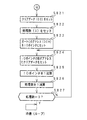
図14は、主基板31におけるCPU56が実行するメイン処理を示すフローチャートである。遊技機に対する電源が投入されると、メイン処理において、CPU56は、まず、必要な初期設定を行う。
【0097】
初期設定処理において、CPU56は、まず、割込禁止に設定する(ステップS1)。次に、割込モードを割込モード2に設定し(ステップS2)、スタックポインタにスタックポインタ指定アドレスを設定する(ステップS3)。そして、内蔵デバイスレジスタの初期化を行う(ステップS4)。また、内蔵デバイス(内蔵周辺回路)であるCTC(カウンタ/タイマ)およびPIO(パラレル入出力ポート)の初期化(ステップS5)を行った後、RAMをアクセス可能状態に設定する(ステップS6)。
【0098】
この実施の形態で用いられているCPU56には、マスク可能な割込(INT)のモードとして以下の3種類のモードが用意されている。なお、マスク可能な割込が発生すると、CPU56は、自動的に割込禁止状態に設定するとともに、プログラムカウンタの内容をスタックにセーブする。
【0099】
割込モード0:割込要求を行った内蔵デバイスがRST命令(1バイト)またはCALL命令(3バイト)をCPUの内部データバス上に送出する。よって、CPU56は、RST命令に対応したアドレスまたはCALL命令で指定されるアドレスの命令を実行する。リセット時に、CPU56は自動的に割込モード0になる。よって、割込モード1または割込モード2に設定したい場合には、初期設定処理において、割込モード1または割込モード2に設定するための処理を行う必要がある。
【0100】
割込モード1:割込が受け付けられると、常に0038(h)番地に飛ぶモードである。
【0101】
割込モード2:CPU56の特定レジスタ(Iレジスタ)の値(1バイト)と内蔵デバイスが出力する割込ベクタ(1バイト:最下位ビット0)から合成されるアドレスが、割込番地を示すモードである。すなわち、割込番地は、上位アドレスが特定レジスタの値とされ下位アドレスが割込ベクタとされた2バイトで示されるアドレスである。従って、任意の(飛び飛びではあるが)偶数番地に割込処理を設置することができる。各内蔵デバイスは割込要求を行うときに割込ベクタを送出する機能を有している。
【0102】
よって、割込モード2に設定されると、各内蔵デバイスからの割込要求を容易に処理することが可能になり、また、プログラムにおける任意の位置に割込処理を設置することが可能になる。さらに、割込モード1とは異なり、割込発生要因毎のそれぞれの割込処理を用意しておくことも容易である。上述したように、この実施の形態では、初期設定処理のステップS2において、CPU56は割込モード2に設定される。
【0103】
そして、電源断時にバックアップRAM領域のデータ保護処理(例えばパリティデータの付加等の停電発生NMI処理)が行われたか否か確認する(ステップS7)。この実施の形態では、不測の電源断が生じた場合には、バックアップRAM領域のデータを保護するための処理が行われている。そのような保護処理が行われていた場合をバックアップありとする。バックアップなしを確認したら、CPU56は初期化処理を実行する。
【0104】
この実施の形態では、バックアップRAM領域にバックアップデータがあるか否かは、電源断時にバックアップRAM領域に設定されるバックアップフラグの状態によって確認される。この例では、図15に示すように、バックアップフラグ領域に「55H」が設定されていればバックアップあり(オン状態)を意味し、「55H」以外の値が設定されていればバックアップなし(オフ状態)を意味する。
【0105】
バックアップありを確認したら、CPU56は、バックアップRAM領域のデータチェック(この例ではパリティチェック)を行う。不測の電源断が生じた後に復旧した場合には、バックアップRAM領域のデータは保存されていたはずであるから、チェック結果は正常になる。チェック結果が正常でない場合には、内部状態を電源断時の状態に戻すことができないので、停電復旧時でない電源投入時に実行される初期化処理を実行する。
【0106】
チェック結果が正常であれば(ステップS8)、CPU56は、遊技制御手段の内部状態と表示制御手段等の電気部品制御手段の制御状態を電源断時の状態に戻すための遊技状態復旧処理を行う(ステップS9)。そして、バックアップRAM領域に保存されていたPC(プログラムカウンタ)の退避値がPCに設定され、そのアドレスに復帰する。
【0107】
初期化処理では、CPU56は、まず、RAMクリア処理を行う(ステップS11)。また、所定の作業領域(例えば、普通図柄判定用乱数カウンタ、普通図柄判定用バッファ、特別図柄左中右図柄バッファ、払出コマンド格納ポインタなど)に初期値を設定する初期値設定処理も行われる。さらに、サブ基板(ランプ制御基板35、払出制御基板37、音声制御基板70、図柄制御基板80)を初期化するための処理を実行する(ステップS13)。サブ基板を初期化する処理とは、例えば初期設定コマンドを送出する処理である。
【0108】
そして、2ms毎に定期的にタイマ割込がかかるようにCPU56に設けられているCTCのレジスタの設定が行われる(ステップS14)。すなわち、初期値として2msに相当する値が所定のレジスタ(時間定数レジスタ)に設定される。そして、初期設定処理のステップS1において割込禁止とされているので、初期化処理を終える前に割込が許可される(ステップS15)。
【0109】
この実施の形態では、CPU56の内蔵CTCが繰り返しタイマ割込を発生するように設定される。この実施の形態では、繰り返し周期は2msに設定される。そして、タイマ割込が発生すると、図16に示すように、CPU56は、例えばタイマ割込が発生したことを示すタイマ割込フラグをセットする(ステップS12)。
【0110】
初期化処理の実行(ステップS11〜S15)が完了すると、メイン処理で、タイマ割込が発生したか否かの監視(ステップS17)の確認が行われるループ処理に移行する。なお、ループ内では、表示用乱数更新処理(ステップS16)も実行される。
【0111】
CPU56は、ステップS17において、タイマ割込が発生したことを認識すると、ステップS21〜S31の遊技制御処理を実行する。遊技制御処理において、CPU56は、まず、スイッチ回路58を介して、ゲートセンサ12、始動口センサ17、カウントセンサ23および入賞口スイッチ19a,19b,24a,24b等のスイッチの状態を入力し、それらの状態判定を行う(スイッチ処理:ステップS21)。
【0112】
次いで、パチンコ遊技機1の内部に備えられている自己診断機能によって種々の異常診断処理が行われ、その結果に応じて必要ならば警報が発せられる(エラー処理:ステップS22)。
【0113】
次に、遊技制御に用いられる大当り判定用の乱数等の各判定用乱数を示す各カウンタを更新する処理を行う(ステップS23)。CPU56は、さらに、停止図柄の種類を決定する乱数等の表示用乱数を更新する処理を行う(ステップS24)。
【0114】
さらに、CPU56は、特別図柄プロセス処理を行う(ステップS25)。特別図柄プロセス制御では、遊技状態に応じてパチンコ遊技機1を所定の順序で制御するための特別図柄プロセスフラグに従って該当する処理が選び出されて実行される。そして、特別図柄プロセスフラグの値は、遊技状態に応じて各処理中に更新される。また、普通図柄プロセス処理を行う(ステップS26)。普通図柄プロセス処理では、7セグメントLEDによる可変表示器10を所定の順序で制御するための普通図柄プロセスフラグに従って該当する処理が選び出されて実行される。そして、普通図柄プロセスフラグの値は、遊技状態に応じて各処理中に更新される。
【0115】
次いで、CPU56は、特別図柄に関する表示制御コマンドをRAM55の所定の領域に設定して表示制御コマンドを送出する処理を行う(特別図柄コマンド制御処理:ステップS27)。また、普通図柄に関する表示制御コマンドをRAM55の所定の領域に設定して表示制御コマンドを送出する処理を行う(普通図柄コマンド制御処理:ステップS28)。
【0116】
さらに、CPU56は、例えばホール管理用コンピュータに供給される大当り情報、始動情報、確率変動情報などのデータを出力する情報出力処理を行う(ステップS29)。
【0117】
また、CPU56は、所定の条件が成立したときにソレノイド回路59に駆動指令を行う(ステップS30)。ソレノイド回路59は、駆動指令に応じてソレノイド16,21を駆動し、可変入賞球装置15または開閉板20を開状態または閉状態とする。
【0118】
そして、CPU56は、各入賞口への入賞を検出するためのスイッチ17,23,19a,19b,24a,24bの検出出力にもとづく賞球数の設定などを行う賞球処理を実行する(ステップS31)。具体的には、入賞検出に応じて払出制御基板37に払出制御コマンドを出力する。払出制御基板37に搭載されている払出制御用CPU371は、払出制御コマンドに応じて球払出装置97を駆動する。
【0119】
以上の制御によって、この実施の形態では、遊技制御処理は2ms毎に起動されることになる。なお、この実施の形態では、タイマ割込処理では例えば割込が発生したことを示すフラグのセットのみがなされ、遊技制御処理はメイン処理において実行されるが、タイマ割込処理で遊技制御処理を実行してもよい。
【0120】
また、メイン処理には遊技制御処理に移行すべきか否かを判定する処理が含まれ、CPU56の内部タイマが定期的に発生するタイマ割込にもとづくタイマ割込処理で遊技制御処理に移行すべきか否かを判定するためのフラグがセット等がなされるので、遊技制御処理の全てが確実に実行される。つまり、遊技制御処理の全てが実行されるまでは、次回の遊技制御処理に移行すべきか否かの判定が行われないので、遊技制御処理中の全ての各処理が実行完了することは保証されている。
【0121】
以上に説明したように、この実施の形態では、CTCやPIOを内蔵するCPU56に対して、初期設定処理で割込モード2が設定される。従って、内蔵CTCを用いた定期的なタイマ割込処理を容易に実現できる。また、タイマ割込処理をプログラム上の任意の位置に設置できる。また、内蔵PIOを用いたスイッチ検出処理等を容易に割込処理で実現できる。その結果、プログラム構成が簡略化され、プログラム開発工数が低減する等の効果を得ることができる。
【0122】
なお、CTCおよびPIOの設定(ステップS5)が完了した後に、IEO/SCLK0端子から出力されるクロック信号の周波数を決めるための内部レジスタの設定を行ってもよい。その際、クロック信号の周波数は、遊技制御処理の起動周期である2msに応じた周波数とされる。そのような設定を行うと、IEO/SCLK0端子から、遊技制御処理の起動周期に応じた周波数のクロック信号がCPU56から外部出力される。すると、CPU56の外部において遊技制御処理の起動周期に対応した信号を観測することができる。よって、そのような信号を用いて、遊技機外部においてCPU56による遊技制御処理をシミュレーションしたり、CPU56の動作状況を試験したりすることが容易になる。
【0123】
また、図11および図12に示された出力ポート0〜6のうち、出力ポート0,1,2,3,4は、遊技制御処理のうちの特別図柄コマンド制御処理(ステップS25)、普通図柄コマンド制御処理(ステップS27)、賞球処理(ステップS31)等でアクセスされる。また、出力ポート5は、情報出力処理(ステップS29)でアクセスされ、出力ポート6は、特別図柄プロセス処理(ステップS25)や普通図柄プロセス処理(ステップS26)でアクセスされる。
【0124】
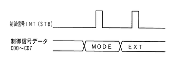
次に、遊技制御手段から各電気部品制御手段に対する制御コマンドの送出方式について説明しておく。図17は、主基板31から他の電気部品制御基板に送出される制御コマンドのコマンド形態の一例を示す説明図である。この実施の形態では、制御コマンドは2バイト構成であり、1バイト目はMODE(コマンドの分類)を表し、2バイト目はEXT(コマンドの種類)を表す。MODEデータの先頭ビット(ビット7)は必ず「1」とされ、EXTデータの先頭ビット(ビット7)は必ず「0」とされる。なお、図17に示されたコマンド形態は一例であって他のコマンド形態を用いてもよい。
【0125】
図18は、遊技制御基板から他の各電気部品制御基板に対する制御コマンドを構成する8ビットの制御信号とINT信号(ストローブ信号)との関係を示すタイミング図である。図18に示すように、MODEまたはEXTのデータが出力ポートに出力されてから、所定期間が経過すると、CPU56は、データ出力を示す信号であるINT信号をオン状態にする。また、そこから所定期間が経過するとINT信号をオフ状態にする。
【0126】
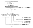
遊技制御手段から払出制御基板等の各電気部品制御基板に制御コマンドを出力しようとするときに、コマンド送信テーブルの設定が行われる。図19(A)は、コマンド送信テーブルの一構成例を示す説明図である。1つのコマンド送信テーブルは3バイトで構成され、1バイト目にはINTデータが設定される。また、2バイト目のコマンドデータ1には、制御コマンドの1バイト目のMODEデータが設定される。そして、3バイト目のコマンドデータ2には、制御コマンドの2バイト目のEXTデータが設定される。
【0127】
なお、EXTデータそのものがコマンドデータ2の領域に設定されてもよいが、コマンドデータ2には、EXTデータが格納されているテーブルのアドレスを指定するためのデータが設定されるようにしてもよい。この実施の形態では、コマンドデータ2のビット7(ワークエリア参照ビット)が0あれば、コマンドデータ2にEXTデータそのものが設定されていることを示す。そのようなEXTデータはビット7が0であるデータである。ワークエリア参照ビットが1あれば、他の7ビットが、EXTデータが格納されているテーブルのアドレスを指定するためのオフセットであることを示す。また、この実施の形態では各制御コマンド毎にコマンド送信テーブルが用意されている。
【0128】
図19(B)INTデータの一構成例を示す説明図である。INTデータにおけるビット0は、払出制御基板37に払出制御コマンドを送出すべきか否かを示す。ビット0が「1」であるならば、払出制御コマンドを送出すべきことを示す。従って、CPU56は、例えば賞球処理において、払出制御コマンドを送出するときには、払出制御コマンド用のコマンド送信テーブルのINTデータに「01(H)」を設定する。
【0129】
INTデータのビット1,2,3は、それぞれ、表示制御コマンド、ランプ制御コマンド、音声制御コマンドを送出すべきか否かを示すビットであり、CPU56は、それらのコマンドを送出すべき場合には、ポインタが指しているコマンド送信テーブルに、INTデータ、コマンドデータ1およびコマンドデータ2を設定する。それらのコマンドを送出するときには、INTデータの該当ビットが「1」に設定され、コマンドデータ1およびコマンドデータ2にMODEデータおよびEXTデータが設定される。
【0130】
各電気部品制御基板への制御コマンドを、対応する出力ポート(出力ポート1〜4)に出力する際に、出力ポート0のビット0〜3のうちのいずれかのビットが所定期間オン状態になるのであるが、INTデータにおけるビット配列と出力ポート0におけるビット配列とは対応している。従って、各電気部品制御基板に御コマンドを送出する際に、コマンド送信テーブルに設定されているINTデータにもとづいて、容易にINT信号の出力を行うことができる。
【0131】
図20,図21は、電源基板910からの電源断信号に応じて実行されるマスク不能割込処理(電力供給停止時処理)の処理例を示すフローチャートである。
【0132】
電力供給停止時処理において、CPU56は、AFレジスタ(アキュミュレータとフラグのレジスタ)を所定のバックアップRAM領域に退避する(ステップS51)。また、割込フラグをパリティフラグにコピーする(ステップS52)。パリティフラグはバックアップRAM領域に形成されている。また、BCレジスタ、DEレジスタ、HLレジスタ、IXレジスタおよびスタックポインタをバックアップRAM領域に退避する(ステップS54〜58)。
【0133】
次に、バックアップあり指定値(この例では「55H」)をバックアップフラグにストアする。バックアップフラグはバックアップRAM領域に形成されている。次いで、パリティデータを作成する(ステップS60〜S67)。すなわち、まず、クリアデータ(00)をチェックサムデータエリアにセットし(ステップS60)、チェックサム算出開始アドレスをポインタにセットする(ステップS61)。また、チェックサム算出回数をセットする(ステップS62)。
【0134】
そして、チェックサムデータエリアの内容とポインタが指すRAM領域の内容との排他的論理和を演算する(ステップS63)。演算結果をチェックサムデータエリアにストアするとともに(ステップS64)、ポインタの値を1増やし(ステップS65)、チェックサム算出回数の値を1減算する(ステップS66)。ステップS63〜S66の処理が、チェックサム算出回数の値が0になるまで繰り返される(ステップS67)。
【0135】
チェックサム算出回数の値が0になったら、CPU56は、チェックサムデータエリアの内容の各ビットの値を反転する(ステップS68)。そして、反転後のデータをチェックサムデータエリアにストアする(ステップS69)。このデータが、電源投入時にチェックされるパリティデータとなる。次いで、RAMアクセスレジスタにアクセス禁止値を設定する(ステップS70)。以後、内蔵RAM55のアクセスができなくなる。
【0136】
さらに、CPU56は、クリアデータ(00)を適当なレジスタにセットし(ステップS71)、処理数(この例では「7」)を別のレジスタにセットする(ステップS72)。また、出力ポート0のアドレスをIOポインタに設定する(ステップS73)。IOポインタとして、さらに別のレジスタが用いられる。
【0137】
そして、IOポインタが指すアドレスにクリアデータをセットするとともに(ステップS74)、IOポインタの値を1増やし(ステップS75)、処理数の値を1減算する(ステップS77)。ステップS74〜S76の処理が、処理数の値が0になるまで繰り返される。その結果、全ての出力ポート0〜6(図11および図12参照)にクリアデータが設定される。図11および図12に示すように、この例では、「1」がオン状態であり、クリアデータである「00」が各出力ポートにセットされるので、全ての出力ポートがオフ状態になる。
【0138】
従って、遊技状態を保存するための処理(この例では、チェックサムの生成およびRAMアクセス防止)が実行された後、各出力ポートは直ちにオフ状態になる。なお、この実施の形態では、遊技制御処理において用いられるデータが格納されるRAM領域は全て電源バックアップされている。従って、その内容が正しく保存されているか否かを示すチェックサムの生成処理、およびその内容を書き換えないようにするためのRAMアクセス防止処理が、遊技状態を保存するための処理に相当する。
【0139】
遊技状態を保存するための処理が実行された後、直ちに各出力ポートがオフ状態になるので、保存される遊技状態と整合しない状況が発生することは確実に防止される。図20に示す処理が実行されるときには、遊技機に対する電源供給が停止するので、電気部品に印加される電圧が低下していく。そして、印加電圧が駆動可能電圧を下回った時点で電気部品の駆動は停止する。従って、遊技機に対する電力供給停止時には、短時間の遅れはあるものの電気部品の駆動は停止する。
【0140】
ところが、この実施の形態のような出力ポートに対するクリア処理を行わないと、遊技状態が保存された後、電力供給が停止するのを遊技制御手段が待っている間に可変入賞球装置15にさらに入賞してしまうこともある。そのような場合、電力供給再開時には保存されている遊技状態が復帰されるので保存時の始動入賞記憶数が始動記憶表示器18に表示される。すると、遊技者から見ると、始動入賞の保留記憶値が少なくなってしまっているように見え、トラブルが発生しかねない。しかし、この実施の形態では、そのようなトラブルが生ずる可能がなくなる。さらに、停電等が発生する直前に大入賞口を開放する制御がなされたまま電力供給停止時処理が実行されて待機ループに入った後、電源が落ちきらないまま復帰したような場合に、この実施の形態では、遊技制御は待機ループに入っているが大入賞口は開いたままになっているという現象が生じてしまうことが防止される。また、待機ループに入っている間に可変表示が開始されてしまう等の現象も防止することができる。
【0141】
また、遊技状態が保存された後に、可変入賞球装置しての大入賞口への入賞が発生する場合もあり得る。そのような場合、遊技者が認識している入賞個数と、電力供給復帰時に、保存されていた遊技状態にもとづいて表示部に表示される入賞個数とが食い違ってトラブルが生ずる可能性もある。しかし、この実施の形態では、そのようなトラブルが生ずる可能がなくなる。
【0142】
出力ポートに対するクリア処理が完了すると、CPU56は、待機状態(ループ状態)に入る。従って、システムリセットされるまで、何もしない状態になる。
【0143】
なお、この実施の形態では、NMIに応じて電力供給停止時処理が実行されたが、電源断信号をCPU56のマスク可能端子に接続し、マスク可能割込処理によって電力供給停止時処理を実行してもよい。また、電源断信号を入力ポートに入力し、入力ポートのチェック結果に応じて電力供給停止時処理を実行してもよい。
【0144】
図22は、遊技機の電源断時の電源低下やNMI割込信号(ここでは、電源断信号)の様子を示すタイミング図である。遊技機に対する電力供給が断たれると、最も高い直流電源電圧であるVSLの電圧値は徐々に低下する。そして、この例では、+22Vにまで低下すると、図8に示された電源基板910に搭載されている電源監視用IC902から電源断信号(電圧低下信号)が出力される(ローレベルになる)。
【0145】
この実施の形態では、電源断信号は、主基板31および払出制御基板37に入力され、CPU56および払出制御用CPU371のNMI端子に入力される。主基板31のCPU56は、マスク不能割込処理によって、上述した電力供給停止時処理を実行する。
【0146】
VSLの電圧値がさらに低下して所定値(この例では+9V)にまで低下すると、図9に示されたように主基板31搭載されているリセットIC651の出力がローレベルになり、CPU56がシステムリセット状態になる。なお、CPU56は、システムリセット状態とされる前に、電力供給停止時処理を完了している。
【0147】
VSLの電圧値がさらに低下してVcc(各種回路を駆動するための+5V)を生成することが可能な電圧を下回ると、各基板において各回路が動作できない状態となる。しかし、主基板31では、電力供給停止時処理が実行され、CPU56がシステムリセット状態とされている。
【0148】
なお、後述するように、払出制御基板37における払出制御用CPU371も、同様に電力供給停止時処理を行った後にシステムリセット状態になる。
【0149】
以下、遊技状態復旧処理について説明する。
図23は、図14のステップS9に示された遊技状態復旧処理の一例を示すフローチャートである。この例では、CPU56は、バックアップRAMに保存されていた値を各レジスタに復元する(ステップS91)。そして、バックアップRAMに保存されていたデータにもとづいて停電時の遊技状態を確認して復帰させる。すなわち、バックアップRAMに保存されていたデータにもとづいて、ソレノイド回路59を介してソレノイド16やソレノイド21を駆動し、始動入賞口14や開閉板20の開閉状態の復旧を行う(ステップS92,S93)。また、電源断中でも保存されていた特別図柄プロセスフラグおよび普通図柄プロセスフラグの値に応じて、電源断時の特別図柄プロセス処理の進行状況および普通図柄プロセス処理の進行状況に対応した制御コマンドを、図柄制御基板80、ランプ制御基板35および音声制御基板70に送出する(ステップS94)。
【0150】
以上のように、遊技状態復旧処理では、復元された内部状態に応じて、各種電気部品の状態復元が行われるとともに、図柄制御基板80、ランプ制御基板35および音声制御基板70に対して、制御状態を電源断時の状態に戻すための制御コマンド(電源断時の制御状態を生じさせるための制御コマンド)が送出される。そのような制御コマンドは、一般に、電源断前に最後に送出された1つまたは複数の制御コマンドである。
【0151】
遊技状態を電源断時の状態に復帰させると、この実施の形態では、CPU56は、前回の電源断時の割込許可/禁止状態を復帰させるため、バックアップRAMに保存されていたパリティフラグの値を確認する(ステップS95)。パリティフラグがオフ状態であれば、割込許可設定を行う(ステップS96)。しかし、パリティフラグがオン状態であれば、そのまま(ステップS1で設定された割込禁止状態のまま)遊技状態復旧処理を終了する。パリティフラグがオン状態であるということは、図20におけるステップS52に示されたように、前回の電源断時に割込禁止状態であったことを意味する。従って、パリティフラグがオン状態である場合には、割込許可はなされない。
【0152】
次に、遊技制御手段以外の電気部品制御手段においてデータ保存処理および復旧処理が行われる場合の例として、払出制御手段においてデータ保存や復旧が行われる場合について説明する。
【0153】
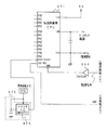
図24は、払出制御用CPU371周りの一構成例を示すブロック図である。図24に示すように、電源基板910の電源監視回路(電源監視手段)からの電源断信号が、バッファ回路960を介して払出制御用CPU371のマスク不能割込端子(XNMI端子)に接続されている。従って、払出制御用CPU371は、マスク不能割込処理によって電源断の発生を確認することができる。
【0154】
払出制御用CPU371のCLK/TRG2端子には、主基板31からのINT信号が接続されている。CLK/TRG2端子にクロック信号が入力されると、払出制御用CPU371に内蔵されているタイマカウンタレジスタCLK/TRG2の値がダウンカウントされる。そして、レジスタ値が0になると割込が発生する。従って、タイマカウンタレジスタCLK/TRG2の初期値を「1」に設定しておけば、INT信号の入力に応じて割込が発生することになる。
【0155】
払出制御基板37には、システムリセット回路975も搭載されているが、この実施の形態では、システムリセット回路975におけるリセットIC976は、電源投入時に、外付けのコンデンサに容量で決まる所定時間だけ出力をローレベルとし、所定時間が経過すると出力をハイレベルにする。また、リセットIC976は、VSLの電源電圧を監視して電圧値が所定値(例えば+9V)以下になると出力をローレベルにする。従って、電源断時には、リセットIC976からの信号がローレベルになることによって払出制御用CPU371がシステムリセットされる。
【0156】
リセットIC976が電源断を検知するための所定値は、通常時の電圧より低いが、払出制御用CPU371が暫くの間動作しうる程度の電圧である。また、リセットIC976が、払出制御用CPU371が必要とする電圧(この例では+5V)よりも高い電圧を監視するように構成されているので、払出制御用CPU371が必要とする電圧に対して監視範囲を広げることができる。従って、より精密な監視を行うことができる。
【0157】
+5V電源から電力が供給されていない間、払出制御用CPU371の内蔵RAMの少なくとも一部は、電源基板から供給されるバックアップ電源がバックアップ端子に接続されることによってバックアップされ、遊技機に対する電源が断しても内容は保存される。そして、+5V電源が復旧すると、システムリセット回路975からリセット信号が発せられるので、払出制御用CPU371は、通常の動作状態に復帰する。そのとき、必要なデータがバックアップされているので、停電等からの復旧時には停電発生時の払出制御状態に復帰することができる。
【0158】
なお、図24に示された構成では、システムリセット回路975は、電源投入時に、コンデンサの容量で決まる期間のローレベルを出力し、その後ハイレベルを出力する。すなわち、リセット解除タイミングは1回だけである。しかし、図9に示された主基板31の場合と同様に、複数回のリセット解除タイミングが発生するような回路構成を用いてもよい。
【0159】
図25は、この実施の形態における出力ポートの割り当てを示す説明図である。図25に示すように、出力ポートC(アドレス00H)は、払出モータ289に出力される駆動信号の出力ポートである。また、出力ポートD(アドレス01H)は、7セグメントLEDであるエラー表示LED374に出力される表示制御信号の出力ポートである。そして、出力ポートE(アドレス02H)は、振分ソレノイド310に出力される駆動信号、およびカードユニット50に対するEXS信号とPRDY信号とを出力するための出力ポートである。
【0160】
図26は、この実施の形態における入力ポートのビット割り当てを示す説明図である。図26に示すように、入力ポートA(アドレス06H)は、主基板31から送出された払出制御コマンドの8ビットの払出制御信号を取り込むための入力ポートである。また、入力ポートB(アドレス07H)のビット0〜2には、それぞれ、賞球カウントスイッチ301A、球貸しカウントスイッチ301B、モータ位置センサの検出信号入力される。ビット3〜5には、カードユニット50からのBRDY信号、BRQ信号およびVL信号が入力される。
【0161】
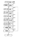
図27は、払出制御用CPU371のメイン処理を示すフローチャートである。メイン処理では、払出制御用CPU371は、まず、必要な初期設定を行う。すなわち、払出制御用CPU371は、まず、割込禁止に設定する(ステップS701)。次に、割込モードを割込モード2に設定し(ステップS702)、スタックポインタにスタックポインタ指定アドレスを設定する(ステップS703)。また、払出制御用CPU371は、内蔵デバイスレジスタの初期化を行い(ステップS704)、CTCおよびPIOの初期化(ステップS705)を行った後に、RAMをアクセス可能状態に設定する(ステップS706)。
【0162】
この実施の形態では、内蔵CTCのうちの一つのチャネルがタイマモードで使用される。従って、ステップS704の内蔵デバイスレジスタの設定処理およびステップS705の処理において、使用するチャネルをタイマモードに設定するためのレジスタ設定、割込発生を許可するためのレジスタ設定および割込ベクタを設定するためのレジスタ設定が行われる。そして、そのチャネルによる割込がタイマ割込として用いられる。タイマ割込を例えば2ms毎に発生させたい場合は、初期値として2msに相当する値が所定のレジスタ(時間定数レジスタ)に設定される。
【0163】
なお、タイマモードに設定されたチャネル(この実施の形態ではチャネル3)に設定される割込ベクタは、タイマ割込処理の先頭番地に相当するものである。具体的は、Iレジスタに設定された値と割込ベクタとでタイマ割込処理の先頭番地が特定される。タイマ割込処理ではタイマ割込フラグがセットされ、メイン処理でタイマ割込フラグがセットされていることが検知されると、払出制御処理が実行される。すなわち、タイマ割込処理では、電気部品制御処理の一例である払出制御処理を実行するための設定がなされる。
【0164】
また、内蔵CTCのうちの他の一つのチャネル(この実施の形態ではチャネル2)が、遊技制御手段からの払出制御コマンド受信のための割込発生用のチャネルとして用いられ、そのチャネルがカウンタモードで使用される。従って、ステップS704の内蔵デバイスレジスタの設定処理およびステップS705の処理において、使用するチャネルをカウンタモードに設定するためのレジスタ設定、割込発生を許可するためのレジスタ設定および割込ベクタを設定するためのレジスタ設定が行われる。
【0165】
カウンタモードに設定されたチャネル(チャネル2)に設定される割込ベクタは、後述するコマンド受信割込処理の先頭番地に相当するものである。具体的は、Iレジスタに設定された値と割込ベクタとでコマンド受信割込処理の先頭番地が特定される。
【0166】
この実施の形態では、払出制御用CPU371でも割込モード2が設定される。従って、内蔵CTCのカウントアップにもとづく割込処理を使用することができる。また、CTCが送出した割込ベクタに応じた割込処理開始番地を設定することができる。
【0167】
CTCのチャネル2(CH2)のカウントアップにもとづく割込は、上述したタイマカウンタレジスタCLK/TRG2の値が「0」になったときに発生する割込である。従って、例えばステップS705において、特定レジスタとしてのタイマカウンタレジスタCLK/TRG2に初期値「1」が設定される。また、CTCのチャネル3(CH3)のカウントアップにもとづく割込は、CPUの内部クロック(システムクロック)をカウントダウンしてレジスタ値が「0」になったら発生する割込であり、後述する2msタイマ割込として用いられる。具体的には、CH3のレジスタ値はシステムクロックの1/256周期で減算される。ステップS705において、CH3のレジスタには、初期値として2msに相当する値が設定される。
【0168】
CTCのCH2のカウントアップにもとづく割込は、CH3のカウントアップにもとづく割込よりも優先順位が高い。従って、同時にカウントアップが生じた場合に、CH2のカウントアップにもとづく割込、すなわち、コマンド受信割込処理の実行契機となる割込の方が優先される。
【0169】
そして、払出制御用CPU371は、払出制御用のバックアップRAM領域にバックアップデータが存在しているか否かの確認を行う(ステップS707)。すなわち、例えば、主基板31のCPU56の処理と同様に、電源断時にセットされるバックアップフラグがセット状態になっているか否かによって、バックアップデータが存在しているか否か確認する。バックアップフラグがセット状態になっている場合には、バックアップデータありと判断する。
【0170】
バックアップありを確認したら、払出制御用CPU371は、バックアップRAM領域のデータチェック(この例ではパリティチェック)を行う。不測の電源断が生じた後に復旧した場合には、バックアップRAM領域のデータは保存されていたはずであるから、チェック結果は正常になる。チェック結果が正常でない場合には、内部状態を電源断時の状態に戻すことができないので、停電復旧時でない電源投入時に実行される初期化処理を実行する。
【0171】
チェック結果が正常であれば(ステップS708)、払出制御用CPU371は、内部状態を電源断時の状態に戻すための払出状態復旧処理を行う(ステップS709)。そして、バックアップRAM領域に保存されていたPC(プログラムカウンタ)の指すアドレスに復帰する。
【0172】
初期化処理では、払出制御用CPU371は、まず、RAMクリア処理を行う(ステップS711)。そして、2ms毎に定期的にタイマ割込がかかるように払出制御用CPU371に設けられているCTCのレジスタの設定が行われる(ステップS712)。すなわち、初期値として2msに相当する値が所定のレジスタ(時間定数レジスタ)に設定される。そして、初期設定処理のステップS701において割込禁止とされているので、初期化処理を終える前に割込が許可される(ステップS713)。
【0173】
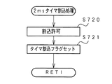
この実施の形態では、払出制御用CPU371の内蔵CTCが繰り返しタイマ割込を発生するように設定される。この実施の形態では、繰り返し周期は2msに設定される。そして、タイマ割込が発生すると、図28に示すように、払出制御用CPU371は、例えばタイマ割込が発生したことを示すタイマ割込フラグをセットする(ステップS721)。なお、図28には割込を許可することも明示されているが(ステップS720)、2msタイマ割込処理では、最初に割込許可状態に設定される。すなわち、2msタイマ割込処理中には割込許可状態になってので、INT信号の入力にもとづく払出制御コマンド受信処理を優先して実行することができる。
【0174】
払出制御用CPU371は、ステップS724において、タイマ割込フラグがセットされたことを検出するとステップS751以降の払出制御処理を実行する。以上の制御によって、この実施の形態では、払出制御処理は2ms毎に起動されることになる。なお、この実施の形態では、タイマ割込処理ではフラグセットのみがなされ、払出制御処理はメイン処理において実行されるが、タイマ割込処理で払出制御処理を実行してもよい。
【0175】
払出制御処理において、払出制御用CPU371は、まず、中継基板72を介して入力ポート372bに入力される賞球カウントスイッチ301A、球貸しカウントスイッチ301Bがオンしたか否かを判定する(スイッチ処理:ステップS751)。
【0176】
次に、払出制御用CPU371は、センサ(例えば、払出モータ289の回転数を検出するモータ位置センサ)からの信号入力状態を確認してセンサの状態を判定する等の処理を行う(入力判定処理:ステップS752)。払出制御用CPU371は、さらに、受信した払出制御コマンドを解析し、解析結果に応じた処理を実行する(コマンド解析実行処理:ステップS753)。
【0177】
次いで、払出制御用CPU371は、主基板31から払出停止指示コマンドを受信していたら払出停止状態に設定し、払出開始指示コマンドを受信していたら払出停止状態の解除を行う(ステップS754)。また、プリペイドカードユニット制御処理を行う(ステップS755)。
【0178】
次いで、払出制御用CPU371は、球貸し要求に応じて貸し球を払い出す制御を行う(ステップS756)。このとき、払出制御用CPU371は、振分ソレノイド310によって球振分部材311を球貸し側に設定する。
【0179】
さらに、払出制御用CPU371は、総合個数記憶に格納された個数の賞球を払い出す賞球制御処理を行う(ステップS757)。このとき、払出制御用CPU371は、振分ソレノイド310によって球振分部材311を賞球側に設定する。そして、出力ポート372cおよび中継基板72を介して球払出装置97の払出機構部分における払出モータ289に対して駆動信号を出力し、所定の回転数分払出モータ289を回転させる払出モータ制御処理を行う(ステップS758)。
【0180】
なお、この実施の形態では、払出モータ289としてステッピングモータが用いられ、それらを制御するために1−2相励磁方式が用いられる。従って、具体的には、払出モータ制御処理において、8種類の励磁パターンデータが繰り返し払出モータ289に出力される。また、この実施の形態では、各励磁パターンデータが4msずつ出力される。
【0181】
次いで、エラー検出処理が行われ、その結果に応じてエラー表示LED374に所定の表示を行う(エラー処理:ステップS759)。
【0182】
なお、出力ポートCは、払出制御処理における払出モータ制御処理(ステップS758)でアクセスされる。また、出力ポートDは、払出制御処理におけるエラー処理(ステップS759)でアクセスされる。そして、出力ポートEは、払出制御処理における球貸し制御処理(ステップS756)および賞球制御処理(ステップS757)でアクセスされる。
【0183】
図29は、払出制御用CPU371が内蔵するRAMの使用例を示す説明図である。この例では、バックアップRAM領域に、総合個数記憶(例えば2バイト)と貸し球個数記憶とがそれぞれ形成されている。総合個数記憶は、主基板31の側から指示された賞球払出個数の総数を記憶するものである。貸し球個数記憶は、未払出の球貸し個数を記憶するものである。
【0184】
このように、未払出の賞球個数と貸し球個数とが、所定期間はその内容を保持可能なバックアップRAM領域に記憶されるので、停電等の不測の電源断が生じても、所定期間内に電源復旧すれば、バックアップRAM領域に記憶される賞球処理および球貸し処理を続行できる。従って、遊技者に与えられる不利益を低減することができる。
【0185】
図30,図31は、電源基板910からの電源断信号に応じて実行されるマスク不能割込処理(電力供給停止時処理)の処理例を示すフローチャートである。
【0186】
電力供給停止時処理において、払出制御用CPU371は、AFレジスタを所定のバックアップRAM領域に退避する(ステップS801)。また、割込フラグをパリティフラグにコピーする(ステップS802)。パリティフラグはバックアップRAM領域に形成されている。また、BCレジスタ、DEレジスタ、HLレジスタ、IXレジスタおよびスタックポインタをバックアップRAM領域に退避する(ステップS804〜808)。
【0187】
次に、バックアップあり指定値(この例では「55H」)をバックアップフラグにストアする。バックアップフラグはバックアップRAM領域に形成されている。次いで、主基板31のCPU56の処理と同様の処理を行ってパリティデータを作成しバックアップRAM領域に保存する(ステップS810〜S819)。そして、RAMアクセスレジスタにアクセス禁止値を設定する(ステップS820)。以後、内蔵RAMのアクセスができなくなる。
【0188】
さらに、払出制御用CPU371は、クリアデータ(00)を適当なレジスタにセットし(ステップS821)、処理数(この例では「3」)を別のレジスタにセットする(ステップS822)。また、出力ポートCのアドレス(この例では「00H」)をIOポインタに設定する(ステップS823)。IOポインタとして、さらに別のレジスタが用いられる。
【0189】
そして、IOポインタが指すアドレスにクリアデータをセットするとともに(ステップS824)、IOポインタの値を1増やし(ステップS825)、処理数の値を1減算する(ステップS827)。ステップS824〜S826の処理が、処理数の値が0になるまで繰り返される。その結果、全ての出力ポートC〜E(図25参照)にクリアデータが設定される。図25に示すように、この例では、「1」がオン状態であり、クリアデータである「00」が各出力ポートにセットされるので、全ての出力ポートがオフ状態になる。
【0190】
従って、遊技状態を保存するための処理(この例では、チェックサムの生成およびRAMアクセス防止)が実行された後、各出力ポートは直ちにオフ状態になる。なお、この実施の形態では、払出制御処理において用いられるデータが格納されるRAM領域は全て電源バックアップされている。従って、その内容が正しく保存されているか否かを示すチェックサムの生成処理、およびその内容を書き換えないようにするためのRAMアクセス防止処理が、払出制御状態を保存するための処理に相当する。
【0191】
制御状態を保存するための処理が実行された後、直ちに各出力ポートがオフ状態になるので、保存される遊技状態と整合しない状況が発生することは確実に防止される。一般に遊技機に対する電源供給が停止するときには、短時間の遅れはあるものの、各電気部品に対する電力供給も停止して動作が停止する。ところが、そのような自然な動作停止を期待すると、不都合が生ずる場合がある。
【0192】
例えば、払出モータ289に対する駆動信号のクリア処理(オフ処理)がなされないと、払出モータ289が動作不能になる電圧にまで電源電圧が低下していく最中で遊技球の払い出しがなされてしまうことがある。ところが、その前の段階で未払出数が保存されているので、電源電圧が復旧して保存されているデータにもとづいて払出処理を続行したのでは、余分に遊技球を払い出してしまうことになる。しかし、この実施の形態では、払出制御状態を保存したら直ちに出力ポートのクリア処理が行われるので、そのような不都合が生ずることを防止することができる。
【0193】
すなわち、この実施の形態では、遊技機への電力供給停止時に制御状態をバックアップ記憶手段に保存するように構成した場合に、制御の矛盾等を生じさせないようにすることができる。
【0194】
出力ポートに対するクリア処理が完了すると、払出制御用CPU371は、待機状態(ループ状態)に入る。従って、システムリセットされるまで、何もしない状態になる。
【0195】
なお、この実施の形態では、NMIに応じて電力供給停止時処理が実行されたが、電源断信号を払出制御用CPU371のマスク可能端子に接続し、マスク可能割込処理によって電力供給停止時処理を実行してもよい。また、電源断信号を入力ポートに入力し、入力ポートのチェック結果に応じて電力供給停止時処理を実行してもよい。
【0196】
以上のように、この実施の形態では、電気部品制御手段が、電力供給が停止する際に実行する電力供給停止時処理で、電気部品の作動を停止させるためのクリア信号を出力する。従って、遊技機への電力供給停止時に保存した制御状態が、遊技機における実際の制御状態と矛盾してしまうようなことが防止される。
【0197】
さらに、この実施の形態では、電気部品の作動を停止させるためのクリア信号を出力する場合に、所定のレジスタ等にクリアデータを設定した後に、出力ポートに対して、レジスタ等に設定されているクリアデータを順次各出力ポートに出力する繰り返し処理が行われる(図21におけるステップS74〜S77、図31におけるステップS824〜S827)。従って、クリア信号出力処理を迅速に行うことができ、遊技機への電力供給停止時に保存した制御状態と実際の制御状態との間の矛盾発生をより効果的に防止できる。
【0198】
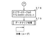
図32は、本発明の他の実施の形態における遊技制御手段のマスク不能割込処理(電力供給停止時処理)の一部を示すフローチャートである。図32に示すフローチャートは、図20に示されたステップS51〜S70の処理に続いて実行される。すなわち、この実施の形態では、RAMアクセス禁止状態に設定された後(ステップS70)、クリアデータテーブルの先頭アドレスがポインタにセットされ(ステップS78)、次いで、データクリア処理が実行された後に(ステップS79)、システムリセットを待つ待機状態に入る。なお、ポインタとして所定のレジスタが用いられる。
【0199】
図33は、クリアデータテーブルの一構成例を示す説明図である。図33に示す例では、クリアデータテーブルには、順に、処理数データ(この例では「7」)、出力ポート0のアドレス、出力ポート0に設定されるべきクリアデータ、・・・、出力ポート6のアドレス、出力ポート6に設定されるべきクリアデータが設定されている。出力ポートのアドレスとクリアデータとは、出力ポートのアドレスが小さいものから順に設定されている。
【0200】
図34は、ステップS79のデータクリア処理を示すフローチャートである。データクリア処理において、CPU56は、ポインタの指すアドレスから処理数データを抽出する(ステップS81)。そして、ポインタの値を1増やす(ステップS82)。次いで、ポインタの指すアドレスからアドレスデータ(出力ポートのアドレス)を抽出する(ステップS83)。さらに、ポインタの値を1増やす(ステップS84)。
【0201】
そして、ポインタの指すアドレスからクリアデータを抽出し(ステップS85)、そのデータを、ステップS83で抽出したアドレスに設定する(ステップS86)。次に、処理数の値を1減算し(ステップS87)、処理数が0になったらデータクリア処理を終了する(ステップS88)。処理数が0でない場合には、ステップS81に戻る。
【0202】
図35は、本発明の他の実施の形態における払出制御手段のクリアデータテーブルを用いたマスク不能割込処理(電力供給停止時処理)の一部を示すフローチャートである。図35に示すフローチャートは、図30に示されたステップS801〜S820の処理に続いて実行される。すなわち、この実施の形態では、RAMアクセス禁止状態に設定された後(ステップS820)、クリアデータテーブルの先頭アドレスがポインタにセットされ(ステップS831)、次いで、データクリア処理が実行された後に(ステップS832)、システムリセットを待つ待機状態に入る。なお、ポインタとして所定のレジスタが用いられる。
【0203】
図36は、クリアデータテーブルの一構成例を示す説明図である。図36に示す例では、クリアデータテーブルには、順に、処理数データ(この例では「3」)、出力ポートCのアドレス(アドレス00H)、出力ポートCに設定されるべきクリアデータ、・・・、出力ポートEのアドレス(アドレス02H)、出力ポートEに設定されるべきクリアデータが設定されている。出力ポートのアドレスとクリアデータとは、出力ポートのアドレスが小さいものから順に設定されている。なお、出力ポートのアドレス割り当ては、規則的に並んだアドレスであれば、1つ飛び等でもよく、そのような場合でも、加算値を変えることによって次アドレスを容易に求めることができる。また、演算は加算に限らず、アドレスの割り当て方等に応じて減算や積算等であってもよい。
【0204】
図37は、ステップS832のデータクリア処理を示すフローチャートである。データクリア処理において、払出制御用CPU371は、ポインタの指すアドレスから処理数データを抽出する(ステップS841)。そして、ポインタの値を1増やす(ステップS842)。次いで、ポインタの指すアドレスからアドレスデータ(出力ポートのアドレス)を抽出する(ステップS843)。さらに、ポインタの値を1増やす(ステップS844)。
【0205】
そして、ポインタの指すアドレスからクリアデータを抽出し(ステップS845)、そのデータを、ステップS843で抽出したアドレスに設定する(ステップS846)。次に、処理数の値を1減算し(ステップS847)、処理数が0になったらデータクリア処理を終了する(ステップS848)。処理数が0でない場合には、ステップS841に戻る。
【0206】
クリアデータテーブルを用いるようにしても、クリア信号出力処理を迅速に行うことができ、遊技機への電力供給停止時に保存した制御状態と実際の制御状態との間の矛盾発生をより効果的に防止できる。そして、クリアデータテーブルを用いる場合には、テーブルにおいて、アドレスデータとクリアデータとをアドレス順に並べなくてもよく、テーブル構成の自由度が増す。例えば、試験信号などを用いる遊技機において試験信号をクリアしないようにしたい場合に、試験信号に関する出力ポートに関するデータをテーブルから除外することによって、容易に試験信号のクリア処理を除外することができる。また、出力ポートの増減や変更があったような場合に、テーブルの内容を変更するだけでよく、プログラム変更の必要はない。
【0207】
なお、クリアデータが全ての出力ポートについて00Hである場合には、クリアデータテーブルにクリアデータを含めなくてもよい。その場合には、図34および図37に示されたデータクリア処理におけるステップSS84,S85およびS844,S845の処理は不要であり、ステップS86およびステップS846において、アドレスデータが指すアドレスにクリアデータ00Hが設定される。
【0208】
以上のように、上記の各実施の形態では、出力ポートをクリアする出力ポートクリア処理が、クリアする出力ポートのアドレスが所定の順序に従って演算によって設定されるように構成されていたり、クリアする出力ポートのアドレスが所定のデータテーブルの内容にもとづいて取得されるように構成されているので、出力ポートのクリア処理を迅速に行うことができる。また、出力ポートクリア処理に関するプログラム容量が削減される。
【0209】
また、特に、電力供給停止時処理において電気部品制御手段がクリア信号を出力するので、各電気部品の作動状態を、保存された遊技状態と矛盾しないようにすることができる。例えば、遊技状態を保存した直後に、開放中の大入賞口を閉成したり、開放中の可変入賞球装置15を閉成したり、駆動状態にある払出モータ289の作動を停止することによって、適切な停止状態で電源復旧を待つことができる。
【0210】
なお、上記の各実施の形態では、出力ポートのクリア処理が電力供給停止時処理で実行される場合を例にしたが、制御進行上の他のタイミングでも、上記の実施の形態の出力ポートクリア処理を適用することができる。例えば、電源投入時の初期化処理において全ての出力ポートをクリアするように構成されている場合に、クリア処理が、クリアする出力ポートのアドレスが所定の順序に従って演算によって設定されるように構成されていたり、クリアする出力ポートのアドレスが所定のデータテーブルの内容にもとづいて取得されるように構成されていてもよい。
【0211】
さらに、上述した各実施の形態では、遊技制御手段以外の他の電気部品制御手段として払出制御手段を例示したが、表示制御手段、音制御手段およびランプ制御手段についても、上述した制御状態保存処理を行うように構成し、電力供給停止時処理においてクリア信号を出力し、それぞれの電気部品制御手段が制御する電気部品の作動を停止するようにしてもよい。そのように構成すれば、他の電気部品制御手段も、停止状態となる前に各電気部品の作動を停止状態にすることができ、適切な停止状態で電源復旧を待つことができる。
【0212】
また、上記の実施の形態では、電源監視回路は電源基板910に設けられたが、電源監視回路は主基板31や払出制御基板37などの電気部品制御基板に設けられていてもよい。電源回路が搭載された電気部品制御基板が構成される場合には、電源基板には電源監視回路は搭載されない。
【0213】
上記の各実施の形態のパチンコ遊技機1は、始動入賞にもとづいて可変表示部9に可変表示される特別図柄の停止図柄が所定の図柄の組み合わせになると所定の遊技価値が遊技者に付与可能になる第1種パチンコ遊技機であったが、始動入賞にもとづいて開放する電動役物の所定領域への入賞があると所定の遊技価値が遊技者に付与可能になる第2種パチンコ遊技機や、始動入賞にもとづいて可変表示される図柄の停止図柄が所定の図柄の組み合わせになると開放する所定の電動役物への入賞があると所定の権利が発生または継続する第3種パチンコ遊技機であっても、本発明を適用できる。
【0214】
さらに、パチンコ遊技機に限られず、スロット機等においても、何らかの動作をする電気部品が備えられている場合などには本発明を適用することができる。
【0215】
【発明の効果】
以上のように、本発明によれば、電気部品制御手段は、遊技機への電力供給が停止する際に所定の電力供給停止時処理を行うことが可能であり、電気部品制御手段が所定のデータを出力するための複数の出力ポートが設けられ、複数の出力ポートにはそれぞれアドレスが割り当てられており、電気部品制御手段が、クリアデータを出力する出力ポートのアドレスデータ、および出力ポートに出力されるクリアデータが各々複数設定されたデータテーブルを有し、電力供給停止時処理にて、複数の出力ポートにクリアデータを出力する出力ポートクリア処理を行うことが可能であり、出力ポートクリア処理では、クリアデータを出力する出力ポートのアドレスを、データテーブルを参照することによって設定し、データテーブルに設定されているクリアデータを出力ポートに出力する処理を繰り返し実行するように構成したので、出力ポートのクリア処理を迅速に行うことができるとともに、出力ポートクリア処理に関するプログラム容量が削減される効果がある。また、各電気部品の作動状態を、保存された遊技状態と矛盾しないようにすることができる。
【0219】
データテーブルに、クリアデータを出力する処理の繰り返し回数を示す回数データも格納されている場合には、ポート数の増減があった場合に、データテーブルを変更するだけでよく、プログラムを変更する必要はない。
【0220】
出力ポートクリア処理によって、外部へ出力する制御に関わる情報の出力データもクリアされるように構成されている場合には、遊技機外部に出力される情報が、遊技機における制御内容と一致することが保証される。
【0221】
出力ポートクリア処理によって可変入賞球装置の駆動が停止するように構成されている場合には、可変入賞球装置が開放したままになるようなことはない。
【0222】
出力ポートクリア処理によって、払出制御手段へのコマンドデータがクリアされるように構成されている場合には、コマンドデータの出力状態が継続してしまうようなことはない。
【図面の簡単な説明】
【図1】 パチンコ遊技機を正面からみた正面図である。
【図2】 パチンコ遊技機の裏面に設けられている各基板を示す説明図である。
【図3】 パチンコ遊技機の機構盤を背面からみた背面図である。
【図4】 機構板に設置されている中間ベースユニット周りの構成を示す正面図である。
【図5】 球払出装置を示す分解斜視図である。
【図6】 遊技制御基板(主基板)の回路構成を示すブロック図である。
【図7】 払出制御基板および球払出装置の構成要素などの賞球に関連する構成要素を示すブロック図である。
【図8】 電源基板の一構成例を示すブロック図である。
【図9】 主基板におけるCPU周りの一構成例を示すブロック図である。
【図10】 CPUの内部構成をより詳細に示すブロック図である。
【図11】 出力ポートのビット割り当ての一例を示す説明図である。
【図12】 出力ポートのビット割り当ての一例を示す説明図である。
【図13】 入力ポートのビット割り当ての一例を示す説明図である。
【図14】 主基板におけるCPUが実行するメイン処理を示すフローチャートである。
【図15】 バックアップフラグと遊技状態復旧処理を実行するか否かとの関係の一例を示す説明図である。
【図16】 2msタイマ割込処理を示すフローチャートである。
【図17】 制御コマンドのコマンド形態の一例を示す説明図である。
【図18】 制御コマンドを構成する8ビットの制御信号とINT信号との関係を示すタイミング図である。
【図19】 コマンド送信テーブルの一構成例を示す説明図である。
【図20】 遊技制御手段における電力供給停止時処理を示すフローチャートである。
【図21】 遊技制御手段における電力供給停止時処理を示すフローチャートである。
【図22】 遊技機の電源断時の電源低下やNMI割込信号の様子を示すタイミング図である。
【図23】 遊技状態復旧処理の一例を示すフローチャートである。
【図24】 電源監視および電源バックアップのための払出制御用CPU周りの一構成例を示すブロック図である。
【図25】 出力ポートのビット割り当ての一例を示す説明図である。
【図26】 入力ポートのビット割り当ての一例を示す説明図である。
【図27】 払出制御基板におけるCPUが実行するメイン処理を示すフローチャートである。
【図28】 2msタイマ割込処理を示すフローチャートである。
【図29】 払出制御手段におけるRAMの一構成例を示す説明図である。
【図30】 払出制御手段における電力供給停止時処理を示すフローチャートである。
【図31】 払出制御手段における電力供給停止時処理を示すフローチャートである。
【図32】 遊技制御手段における電力供給停止時処理の他の例を示すフローチャートである。
【図33】 クリアデータテーブルの一構成例を示す説明図である。
【図34】 データクリア処理を示すフローチャートである。
【図35】 払出制御手段における電力供給停止時処理の他の例を示すフローチャートである。
【図36】 クリアデータテーブルの一構成例を示す説明図である。
【図37】 データクリア処理を示すフローチャートである。
【符号の説明】
31 遊技制御基板(主基板)
37 払出制御基板
54 ROM
55 RAM
56 CPU
57 I/Oポート
371 払出制御用CPU[0001]
BACKGROUND OF THE INVENTION
The present invention relates to a gaming machine such as a pachinko gaming machine, a coin gaming machine, or a slot machine in which a game is performed according to a player's operation, and more particularly, according to a player's operation in a gaming area on a gaming board. The present invention relates to a gaming machine in which a game is performed.
[0002]
[Prior art]
As an example of a gaming machine, a game medium such as a game ball is launched into a game area by a launching device, and when a game medium is won in a prize area such as a prize opening provided in the game area, a predetermined number of prize balls are awarded to the player There are things that will be paid out. Further, a variable display unit capable of changing the display state is provided, and is configured to give a predetermined game value to the player when the display result of the variable display unit becomes a predetermined specific display mode There is.
[0003]
The game value means that the state of the variable winning ball device provided in the gaming area of the gaming machine is advantageous to a player who is easy to win and a right to become advantageous to the player. Or a condition that the conditions for paying out premium game media are easily established.
[0004]
In the first type pachinko gaming machine having a variable display unit that displays a special symbol, the display result of the variable display unit that displays the special symbol is usually a combination of a specific display mode defined in advance. " When the big hit occurs, for example, the big winning opening is opened a predetermined number of times, and the game shifts to a big hit gaming state where the hit ball is easy to win. And in each open period, if there is a prize for a predetermined number (for example, 10) of the big prize opening, the big prize opening is closed. And the number of times the special winning opening is opened is fixed to a predetermined number (for example, 16 rounds). An opening time (for example, 29.5 seconds) is determined for each opening, and even if the number of winnings does not reach a predetermined number, the big winning opening is closed when the opening time elapses. Further, when a predetermined condition (for example, winning in the V zone provided in the big prize opening) is not established at the time when the big prize opening is closed, the big hit gaming state is ended.
[0005]
In addition, among the combinations of display modes other than the “big hit” combination, the display results that are already deterministic or temporary at the stage where some of the display results of the plurality of variable display portions are not yet derived and displayed. A state in which the display mode of the variable display unit in which “” is derived and displayed satisfies a display condition that is a combination of specific display modes is referred to as “reach”. Then, when the display result of the identification information variably displayed on the variable display section does not satisfy the condition of “big hit”, it becomes “disconnected”, and the variable display state ends. A player plays a game while enjoying how to generate a big hit.
[0006]
When a game ball wins a winning opening provided on the game board, a predetermined number of prize balls are paid out. Since the progress of the game is controlled by the game control means mounted on the main board, the number of winning balls based on the winning is determined by the game control means and transmitted to the payout control board. In the following description, the game control means and other control means control various electrical components provided in the gaming machine, so they may be referred to as electrical component control means.
[0007]
[Problems to be solved by the invention]
As described above, various electrical component control means including game control means are mounted in the gaming machine. In general, each electrical component control means includes a microcomputer. Such an electrical component control means generally performs an initialization process and starts control from an initial state when a power supply voltage rises. Then, an unexpected power interruption such as a power failure occurs, and thereafter, when the power is restored, the state returns to the initial state, which may cause a problem such as loss of the game value obtained by the player. In order to prevent such a problem from occurring, the game control is interrupted in accordance with a predetermined signal generated along with a decrease in the power supply voltage value, and the power supply to the gaming machine is stopped at that time. In particular, it may be controlled to store in a storage means (backup storage means) that is backed up and wait for the power supply to be completely stopped. Such a gaming machine resumes the game based on the saved game state when the power supply is resumed while the game state is saved in the storage means, so that a disadvantage is given to the player. Is prevented.
[0008]
However, if the electrical component is in operation immediately before the processing to save the gaming state in the backup storage means and wait for the power supply to stop, the electrical component control means until the power supply is stopped. A signal indicating the operating state is given to. Then, even if the gaming state that should be restored when power supply is resumed is saved, a situation may occur in which the game is further continued. For example, when the start winning opening which is a variable display start condition in the variable display unit is a variable winning ball device driven by a solenoid or the like, the stored value of the winning ball in the variable winning ball device is stored. Nevertheless, there may be a case where the variable winning ball apparatus as the starting winning opening is further won while the game control means is waiting for the power supply to stop. In such a case, the saved gaming state is restored when the power supply is resumed. From the player's point of view, it seems that the stored value of the start winning prize has decreased, which may cause trouble. .
[0009]
Therefore, an object of the present invention is to provide a gaming machine that can appropriately set the operating state of an electrical component and store an appropriate gaming state when the power supply is unexpectedly cut off. In addition, an object of the present invention is to provide a gaming machine that can efficiently execute initialization processing of an output port for outputting a control signal to an electrical component.
[0010]
[Means for Solving the Problems]
A gaming machine according to the present invention is a gaming machine in which a player can perform a predetermined game, Electrical components for controlling electrical components provided in gaming machines Control means When , Power supply monitoring means for monitoring a power supply voltage of a predetermined potential power supply used in a gaming machine and outputting a voltage drop signal to the electrical component control means when the power supply voltage becomes a predetermined value or less. , Electrical component The control means Depending on the input of the voltage drop signal from the power monitoring means, Perform processing when a predetermined power supply is stopped No , Electrical component The control means is provided with a plurality of output ports for outputting predetermined data, and an address is assigned to each of the plurality of output ports, Electrical component The control means There is a data table in which a plurality of output port address data that outputs clear data and a plurality of clear data output to the output port are set, Multiple output ports during power supply stop processing In clear Output data Output port clear processing can be performed. Output data Output port address The Set by referring to the data table And repeatedly execute the process of outputting the clear data set in the data table to the output port. It is characterized by that.
[0014]
De The data table may also store frequency data indicating the number of repetitions of the process of outputting the clear data.
[0015]
By the output port clear process, for example, Output to the outside Output data of information related to control is cleared.
[0016]
The electrical component control means includes a game control means for controlling the progress of the game, and is provided with an output port for the game control means to output predetermined data. It is possible to perform port clear processing, It is preferable that the driving of the variable winning ball apparatus is stopped by the output port clear process.
[0017]
The electrical component control means includes a game control means for controlling the progress of the game and a payout control means for controlling the payout means for paying out the game medium, and an output port is provided for the game control means to output predetermined data. The game control means can perform the output port clear process in the power supply stop process. By the output port clear process, To payout control means The command data is preferably cleared.
[0020]
DETAILED DESCRIPTION OF THE INVENTION
Hereinafter, an embodiment of the present invention will be described with reference to the drawings.
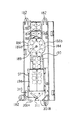
First, the overall configuration of a pachinko gaming machine that is an example of a gaming machine will be described. FIG. 1 is a front view of the
[0021]
As shown in FIG. 1, the
[0022]
Near the center of the
[0023]
An open /
[0024]
The
[0025]
In this example, a
[0026]
The
[0027]
The hit ball fired from the hit ball launching device enters the
[0028]
The rotation of the image in the
[0029]
When the combination of images in the
[0030]
Next, each board | substrate arrange | positioned at the back surface of the
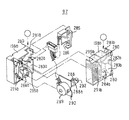
As shown in FIG. 2, on the back surface of the
[0031]
On the back side of the gaming machine, there are installed a variable
[0032]
Furthermore, a power supply board 910 on which a power supply circuit for generating DC30V, DC21V, DC12V and DC5V is mounted is provided, and a
[0033]
FIG. 3 is a rear view of the mechanism plate of the
[0034]
The game balls paid out from the
[0035]
A lot of prize balls based on the winnings are paid out, the hitting
[0036]
Next, the configuration of the intermediate base unit installed on the
[0037]
A
[0038]
The ball break switches 187a and 187b are locked by locking pieces 188 at positions where it can be detected that about 27 to 28 game balls are present in the
[0039]
The central portion of the
[0040]
Below the
[0041]
FIG. 5 is an exploded perspective view of the
[0042]
As shown in FIG. 5, the
[0043]
The
[0044]
In addition, below the ball
[0045]
[0046]
A recess is formed at the tip of the
[0047]
In other words, the payout motor position sensor including the
[0048]
When the
[0049]
As shown in FIG. 4, a
[0050]
In this way, by providing the
[0051]
In this embodiment, a
[0052]
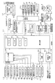
FIG. 6 is a block diagram illustrating an example of a circuit configuration in the main board 31. 6 also shows a
[0053]
Although not shown in FIG. 6, the count switch short-circuit signal is also transmitted to the basic circuit 53 via the
[0054]
Further, according to the data given from the basic circuit 53, the jackpot information indicating the occurrence of the jackpot, the effective starting information indicating the number of starting winning balls used for starting the image display of the
[0055]
The basic circuit 53 includes a
[0056]
Further, the main board 31 is provided with a
[0057]
A ball hitting device for hitting and launching a game ball is driven by a
[0058]
In this embodiment, the lamp control means mounted on the
[0059]
FIG. 7 is a block diagram showing components related to payout, such as components of the
[0060]
The CPU 56 of the main board 31 issues a payout prohibition when the detection signal from the ball break
[0061]
Further, the detection signal from the prize
[0062]
When there is a winning, a payout control command indicating the number of winning balls is input to the
In this embodiment, the payout control CPU 371 is a one-chip microcomputer and incorporates at least a RAM.
[0063]
In the main board 31,
[0064]
The payout control CPU 371 outputs a ball lending number signal indicating the number of lending balls to the
[0065]
Further, a detection signal from the ball lending
[0066]
The
[0067]
A ball lending switch signal and a return switch signal are given from the
[0068]
When the power of the
[0069]
Then, the payout control CPU 371 of the
[0070]
As described above, all signals from the
[0071]
In this embodiment, the case where the
[0072]
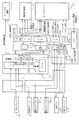
FIG. 8 is a block diagram illustrating a configuration example of the power supply substrate 910. The power supply board 910 is installed independently of the electric component control boards such as the main board 31, the
[0073]
The transformer 911 converts AC voltage from the AC power source into 24V. The AC 24V voltage is output to the connector 915. The rectifier circuit 912 also generates a DC voltage of +30 V from AC 24 V and outputs it to the DC-DC converter 913 and the connector 915. The DC-DC converter 913 generates + 21V, + 12V, and + 5V and outputs them to the connector 915. The connector 915 is connected to, for example, a relay board, and power of a voltage necessary for each electric component control board and the mechanism component is supplied from the relay board.
[0074]
However, each connector reaching each electric component control board may be provided on the power supply board 910 to supply each voltage from the power supply board 910 to each board without going through the relay board. Further, although one connector 915 is representatively shown in FIG. 8, the connector is provided for each electrical component control board.
[0075]
The + 5V line from the DC-DC converter 913 branches to form a backup + 5V line. A large-capacitance capacitor 916 is connected between the backup + 5V line and the ground level. The capacitor 916 is in a storage state with respect to the backup RAM of the electrical component control board when the power supply to the gaming machine is cut off (a RAM that is backed up, that is, a backup storage means that can be in a storage content holding state even when power supply is stopped). It becomes a backup power supply that supplies power so that it can be maintained. Further, a
[0076]
A battery that can be charged from a + 5V power supply may be used as the backup power supply. In the case of using a battery, a rechargeable battery is used in which the capacity disappears when a state in which no power is supplied from the +5 V power source continues for a predetermined time.
[0077]
Further, a power
[0078]
The predetermined value for the
[0079]
Therefore, when the voltage of the + 12V power supply decreases, the switch output becomes in the on state. However, if the power supply interruption is recognized by monitoring the + 30V power supply voltage that decreases faster than + 12V, the power supply is turned on before the switch output shows the on state. It is possible to enter a state of waiting for recovery and not detect switch output.
[0080]
Further, since the
[0081]
In the configuration shown in FIG. 8, the detection output (power cut-off signal) of the
[0082]
FIG. 9 is a block diagram illustrating a configuration example around the CPU 56 in the main board 31. As shown in FIG. 9, the power-off signal (voltage drop signal) from the power supply monitoring circuit (power supply monitoring means) on the power supply board 910 is connected to the non-maskable interrupt terminal (XNMI terminal) of the CPU 56. The power supply monitoring circuit is a circuit that detects a power supply voltage drop by monitoring the voltage of any of the various DC power supplies used by the gaming machine. In this embodiment, the power supply voltage of VSL is monitored, and when the voltage value falls below a predetermined value, a low-level power cut-off signal is generated. VSL is the largest DC voltage used in gaming machines, and is + 30V in this example. Therefore, the CPU 56 can confirm the occurrence of power interruption by the interrupt process.
[0083]
FIG. 9 also shows a
[0084]
As shown in FIG. 9, the reset signal from the reset IC 651 is input to the NAND circuit 947 and also input to the clear terminal of the counter IC 941 via the inverting circuit (NOT circuit) 944. The counter IC 941 counts the clock signal from the
[0085]
For example, the detection voltage of the power supply monitoring circuit (the voltage that outputs the power-off signal) is + 22V, and the detection voltage for setting the reset signal to low level is + 9V. In such a configuration, since the power supply monitoring circuit and the system reset
[0086]
While power is not supplied from the + 5V power source that is the driving power source of the CPU 56 or the like, at least a part of the RAM is backed up by the backup power source supplied from the power supply board, and the contents are preserved even if the power to the gaming machine is cut off The When the +5 V power supply is restored, a reset signal is issued from the system reset
[0087]
In the configuration shown in FIG. 9, two reset signals (low level signals) are given to the reset terminal of the CPU 56 when the power is turned on, but the reset is reliably released even if the reset signal rises only once. When the CPU is used, the circuit elements denoted by reference numerals 941 to 949 are not necessary. In that case, the output of the reset IC 651 is directly connected to the reset terminal of the CPU 56.
[0088]
The CPU 56 used in this embodiment also incorporates an I / O port (PIO) and a timer / counter circuit (CTC). The PIO has 4 bits PB0 to PB3 and 1 byte port PA0 to PA7. The ports PB0 to PB3 and PA0 to PA7 can be set to either input / output.
[0089]
FIG. 10 is a block diagram showing the internal configuration of the CPU 56 in more detail. The CPU core 501 has a register and performs arithmetic processing according to a program. The clock generator 502 divides a clock signal supplied from the outside and supplies it to each built-in device. The clock generator 502 can output a 1/2 frequency-divided clock as a system clock from the CLKO terminal, and can output a clock signal obtained by dividing the system clock from the IEO / SCLK0 terminal via the
[0090]
The reset interrupt controller 503 notifies the CPU core 501 of a system reset signal input to the XRST terminal, a non-maskable interrupt request signal input to the XNMI terminal, and the like. The
[0091]
The memory control circuit 510 generates signals for controlling the built-in
[0092]
The
[0093]
FIG. 11 and FIG. 12 are explanatory diagrams showing assignment of output ports in this embodiment. As shown in FIG. 11, the
[0094]
Further, various information output signals from the
[0095]
FIG. 13 is an explanatory diagram showing bit assignment of input ports in this embodiment. As shown in FIG. 13, the winning
[0096]
Next, the operation of the gaming machine will be described.
FIG. 14 is a flowchart showing main processing executed by the CPU 56 on the main board 31. When the power to the gaming machine is turned on, in the main process, the CPU 56 first performs necessary initial settings.
[0097]
In the initial setting process, the CPU 56 first sets the interrupt prohibition (step S1). Next, the interrupt mode is set to interrupt mode 2 (step S2), and a stack pointer designation address is set to the stack pointer (step S3). Then, the built-in device register is initialized (step S4). Further, after initialization (step S5) of CTC (counter / timer) and PIO (parallel input / output port) which are built-in devices (built-in peripheral circuits), the RAM is set in an accessible state (step S6).
[0098]
The CPU 56 used in this embodiment has the following three types of maskable interrupt (INT) modes. When a maskable interrupt occurs, the CPU 56 automatically sets the interrupt disabled state and saves the contents of the program counter in the stack.
[0099]
Interrupt mode 0: The built-in device that has issued the interrupt request sends an RST instruction (1 byte) or a CALL instruction (3 bytes) onto the internal data bus of the CPU. Therefore, the CPU 56 executes the instruction at the address corresponding to the RST instruction or the address specified by the CALL instruction. At reset, the CPU 56 automatically enters interrupt
[0100]
Interrupt mode 1: In this mode, when an interrupt is accepted, the mode always jumps to address 0038 (h).
[0101]
Interrupt mode 2: A mode in which the address synthesized from the value (1 byte) of the specific register (I register) of the CPU 56 and the interrupt vector (1 byte: least significant bit 0) output by the built-in device indicates the interrupt address It is. That is, the interrupt address is an address indicated by 2 bytes in which the upper address is the value of the specific register and the lower address is the interrupt vector. Therefore, an interrupt process can be set at an arbitrary address (although it is skipped). Each built-in device has a function of sending an interrupt vector when making an interrupt request.
[0102]
Therefore, when the interrupt
[0103]
Then, it is confirmed whether or not data protection processing (for example, power failure occurrence NMI processing such as addition of parity data) has been performed in the backup RAM area when the power is turned off (step S7). In this embodiment, when an unexpected power failure occurs, processing for protecting data in the backup RAM area is performed. When such protection processing is performed, it is assumed that there is a backup. When it is confirmed that there is no backup, the CPU 56 executes an initialization process.
[0104]
In this embodiment, whether or not there is backup data in the backup RAM area is confirmed by the state of the backup flag set in the backup RAM area when the power is turned off. In this example, as shown in FIG. 15, if “55H” is set in the backup flag area, it means that there is a backup (ON state), and if a value other than “55H” is set, there is no backup (OFF). State).
[0105]
After confirming that there is a backup, the CPU 56 performs a data check of the backup RAM area (parity check in this example). In the case of recovery after an unexpected power failure, the data in the backup RAM area should have been saved, so the check result is normal. If the check result is not normal, the internal state cannot be returned to the state at the time of power-off, and therefore an initialization process that is executed at the time of power-on not at the time of power failure recovery is executed.
[0106]
If the check result is normal (step S8), the CPU 56 performs a game state restoration process for returning the internal state of the game control means and the control state of the electric component control means such as the display control means to the state when the power is cut off. (Step S9). Then, the saved value of the PC (program counter) stored in the backup RAM area is set in the PC, and the address is restored.
[0107]
In the initialization process, the CPU 56 first performs a RAM clear process (step S11). Also, initial value setting processing is performed for setting initial values in predetermined work areas (for example, a normal symbol determination random number counter, a normal symbol determination buffer, a special symbol left middle right symbol buffer, a payout command storage pointer, etc.). Further, processing for initializing the sub-boards (
[0108]
Then, a CTC register set in the CPU 56 is set so that a timer interrupt is periodically generated every 2 ms (step S14). That is, a value corresponding to 2 ms is set in a predetermined register (time constant register) as an initial value. Since interruption is prohibited in step S1 of the initial setting process, interruption is permitted before the initialization process is completed (step S15).
[0109]
In this embodiment, the built-in CTC of the CPU 56 is set to repeatedly generate a timer interrupt. In this embodiment, the repetition period is set to 2 ms. When a timer interrupt occurs, as shown in FIG. 16, the CPU 56 sets, for example, a timer interrupt flag indicating that a timer interrupt has occurred (step S12).
[0110]
When the execution of the initialization process (steps S11 to S15) is completed, the main process shifts to a loop process in which it is confirmed whether or not a timer interrupt has occurred (step S17). In the loop, display random number update processing (step S16) is also executed.
[0111]
When the CPU 56 recognizes that a timer interrupt has occurred in step S17, it executes the game control process of steps S21 to S31. In the game control process, the CPU 56 first inputs the states of the switches such as the
[0112]
Next, various abnormality diagnosis processing is performed by the self-diagnosis function provided in the
[0113]
Next, a process of updating each counter indicating each determination random number such as a big hit determination random number used for game control is performed (step S23). The CPU 56 further performs a process of updating a display random number such as a random number that determines the type of stop symbol (step S24).
[0114]
Further, the CPU 56 performs special symbol process processing (step S25). In the special symbol process control, corresponding processing is selected and executed according to a special symbol process flag for controlling the
[0115]
Next, the CPU 56 performs a process of setting a display control command related to the special symbol in a predetermined area of the
[0116]
Further, the CPU 56 performs information output processing for outputting data such as jackpot information, start information, probability variation information supplied to the hall management computer, for example (step S29).
[0117]
Further, the CPU 56 issues a drive command to the solenoid circuit 59 when a predetermined condition is established (step S30). The solenoid circuit 59 drives the
[0118]
Then, the CPU 56 executes a prize ball process for setting the number of prize balls based on the detection outputs of the
[0119]
With the above control, in this embodiment, the game control process is started every 2 ms. In this embodiment, in the timer interrupt process, for example, only a flag indicating that an interrupt has occurred is set, and the game control process is executed in the main process, but the game control process is performed in the timer interrupt process. May be executed.
[0120]
In addition, the main process includes a process for determining whether or not to shift to the game control process, and whether or not the CPU 56 should shift to the game control process by the timer interrupt process based on the timer interrupt generated periodically. Since the flag for determining whether or not is set or the like, all of the game control processing is surely executed. In other words, until all the game control processes are executed, it is not determined whether or not to shift to the next game control process, so it is guaranteed that all the processes in the game control process are completed. ing.
[0121]
As described above, in this embodiment, the interrupt
[0122]
Note that after the setting of CTC and PIO (step S5) is completed, an internal register for determining the frequency of the clock signal output from the IEO / SCLK0 terminal may be set. At that time, the frequency of the clock signal is set to a frequency corresponding to 2 ms which is the start cycle of the game control process. When such setting is performed, a clock signal having a frequency corresponding to the activation period of the game control process is externally output from the CPU 56 from the IEO / SCLK0 terminal. Then, a signal corresponding to the start cycle of the game control process can be observed outside the CPU 56. Therefore, it becomes easy to simulate a game control process by the CPU 56 and to test an operation state of the CPU 56 outside the gaming machine using such a signal.
[0123]
Also, among the
[0124]
Next, a method for sending a control command from the game control means to each electric component control means will be described. FIG. 17 is an explanatory diagram showing an example of a command form of a control command sent from the main board 31 to another electrical component control board. In this embodiment, the control command has a 2-byte configuration, the first byte represents MODE (command classification), and the second byte represents EXT (command type). The first bit (bit 7) of the MODE data is always “1”, and the first bit (bit 7) of the EXT data is always “0”. Note that the command form shown in FIG. 17 is an example, and other command forms may be used.
[0125]
FIG. 18 is a timing diagram showing the relationship between an 8-bit control signal and an INT signal (strobe signal) that constitute a control command from the game control board to each of the other electrical component control boards. As shown in FIG. 18, when a predetermined period elapses after MODE or EXT data is output to the output port, the CPU 56 turns on an INT signal that is a signal indicating data output. Further, when a predetermined period has elapsed from that point, the INT signal is turned off.
[0126]
When a control command is to be output from the game control means to each electrical component control board such as a payout control board, the command transmission table is set. FIG. 19A is an explanatory diagram illustrating a configuration example of the command transmission table. One command transmission table is composed of 3 bytes, and INT data is set in the first byte. In the
[0127]
Although the EXT data itself may be set in the area of the
[0128]
FIG. 19B is an explanatory diagram illustrating a configuration example of INT data.
[0129]
[0130]
When a control command for each electric component control board is output to the corresponding output port (
[0131]
20 and 21 are flowcharts showing a processing example of a non-maskable interrupt process (power supply stop process) executed in response to a power-off signal from the power supply board 910.
[0132]
In the power supply stop process, the CPU 56 saves the AF register (accumulator and flag register) in a predetermined backup RAM area (step S51). Further, the interrupt flag is copied to the parity flag (step S52). The parity flag is formed in the backup RAM area. Further, the BC register, DE register, HL register, IX register and stack pointer are saved in the backup RAM area (steps S54 to S58).
[0133]
Next, the backup specified value ("55H" in this example) is stored in the backup flag. The backup flag is formed in the backup RAM area. Next, parity data is created (steps S60 to S67). That is, first, the clear data (00) is set in the checksum data area (step S60), and the checksum calculation start address is set in the pointer (step S61). Also, the number of checksum calculations is set (step S62).
[0134]
Then, the exclusive OR of the contents of the checksum data area and the contents of the RAM area pointed to by the pointer is calculated (step S63). The calculation result is stored in the checksum data area (step S64), the pointer value is incremented by 1 (step S65), and the value of the checksum calculation count is decremented by 1 (step S66). The processes in steps S63 to S66 are repeated until the value of the checksum calculation count becomes 0 (step S67).
[0135]
When the value of the checksum calculation count becomes 0, the CPU 56 inverts the value of each bit of the contents of the checksum data area (step S68). Then, the inverted data is stored in the checksum data area (step S69). This data becomes parity data to be checked when the power is turned on. Next, an access prohibition value is set in the RAM access register (step S70). Thereafter, the built-in
[0136]
Further, the CPU 56 sets the clear data (00) in an appropriate register (step S71), and sets the number of processes (in this example, “7”) in another register (step S72). Further, the address of the
[0137]
Then, clear data is set at the address pointed to by the IO pointer (step S74), the value of the IO pointer is incremented by 1 (step S75), and the value of the processing number is subtracted by 1 (step S77). The processes in steps S74 to S76 are repeated until the value of the number of processes becomes zero. As a result, clear data is set in all the
[0138]
Therefore, after the processing for saving the game state (in this example, checksum generation and RAM access prevention) is executed, each output port is immediately turned off. In this embodiment, the RAM area in which data used in the game control process is stored is all backed up. Therefore, the checksum generation process indicating whether or not the contents are correctly stored and the RAM access prevention process for preventing the contents from being rewritten correspond to the process for storing the gaming state.
[0139]
Since each output port is turned off immediately after the processing for saving the gaming state is executed, it is reliably prevented that a situation that does not match the saved gaming state occurs. When the process shown in FIG. 20 is executed, the power supply to the gaming machine is stopped, so that the voltage applied to the electrical component decreases. When the applied voltage falls below the drivable voltage, the driving of the electrical component is stopped. Therefore, when the power supply to the gaming machine is stopped, the driving of the electrical components is stopped although there is a short delay.
[0140]
However, if the clear process for the output port as in this embodiment is not performed, the variable winning ball device 15 is further added while the game control means waits for the power supply to stop after the game state is saved. You may win a prize. In such a case, when the power supply is resumed, the saved gaming state is restored, so that the starting winning memory number at the time of saving is displayed on the starting
[0141]
In addition, after the game state is saved, there may be a case where a winning in a big winning opening as a variable winning ball apparatus occurs. In such a case, there is a possibility that a trouble may occur due to a difference between the number of winnings recognized by the player and the number of winnings displayed on the display unit based on the stored gaming state when power supply is restored. However, in this embodiment, there is no possibility of such a trouble occurring.
[0142]
When the clear process for the output port is completed, the CPU 56 enters a standby state (loop state). Therefore, nothing is done until the system is reset.
[0143]
In this embodiment, the power supply stop process is executed according to the NMI. However, the power supply stop signal is connected to the maskable terminal of the CPU 56 and the power supply stop process is executed by the maskable interrupt process. May be. Alternatively, a power-off signal may be input to the input port and the power supply stop process may be executed according to the input port check result.
[0144]
FIG. 22 is a timing chart showing the state of a power supply drop or an NMI interrupt signal (here, a power-off signal) when the gaming machine is powered off. When the power supply to the gaming machine is cut off, the voltage value of VSL, which is the highest DC power supply voltage, gradually decreases. In this example, when the voltage drops to +22 V, a power cut-off signal (voltage drop signal) is output from the
[0145]
In this embodiment, the power-off signal is input to the main board 31 and the
[0146]
When the voltage value of VSL further decreases to a predetermined value (+9 V in this example), the output of the reset IC 651 mounted on the main board 31 becomes low level as shown in FIG. Reset state. Note that the CPU 56 has completed the power supply stop process before entering the system reset state.
[0147]
When the voltage value of VSL is further decreased to be lower than a voltage capable of generating Vcc (+5 V for driving various circuits), each circuit cannot be operated on each substrate. However, in the main board 31, the power supply stop process is executed, and the CPU 56 is in a system reset state.
[0148]
As will be described later, the payout control CPU 371 on the
[0149]
Hereinafter, the gaming state restoration process will be described.
FIG. 23 is a flowchart showing an example of the gaming state recovery process shown in step S9 of FIG. In this example, the CPU 56 restores the value stored in the backup RAM to each register (step S91). Then, based on the data stored in the backup RAM, the gaming state at the time of power failure is confirmed and returned. That is, based on the data stored in the backup RAM, the
[0150]
As described above, in the game state restoration process, the state of various electrical components is restored according to the restored internal state, and control is performed on the
[0151]
In this embodiment, when the gaming state is restored to the power-off state, the CPU 56 returns the value of the parity flag stored in the backup RAM in order to restore the interrupt enable / disable state at the previous power-off. Is confirmed (step S95). If the parity flag is off, interrupt permission is set (step S96). However, if the parity flag is in the on state, the gaming state restoration process is terminated as it is (while keeping the interrupt prohibited state set in step S1). The fact that the parity flag is in the ON state means that the interrupt was prohibited at the previous power-off as shown in step S52 in FIG. Therefore, when the parity flag is in the on state, no interrupt is permitted.
[0152]
Next, as an example of the case where the data storage process and the recovery process are performed in the electrical component control means other than the game control means, the case where the data storage and recovery is performed in the payout control means will be described.
[0153]
FIG. 24 is a block diagram illustrating a configuration example around the payout control CPU 371. As shown in FIG. 24, the power-off signal from the power supply monitoring circuit (power supply monitoring means) of the power supply board 910 is connected to the non-maskable interrupt terminal (XNMI terminal) of the payout control CPU 371 via the
[0154]
The INT signal from the main board 31 is connected to the CLK / TRG2 terminal of the payout control CPU 371. When a clock signal is input to the CLK / TRG2 terminal, the value of the timer counter register CLK / TRG2 built in the payout control CPU 371 is down-counted. When the register value becomes 0, an interrupt occurs. Therefore, if the initial value of the timer counter register CLK / TRG2 is set to “1”, an interrupt is generated according to the input of the INT signal.
[0155]
Although the system reset
[0156]
The predetermined value for the
[0157]
While power is not supplied from the + 5V power supply, at least a part of the built-in RAM of the payout control CPU 371 is backed up by connecting the backup power supplied from the power supply board to the backup terminal, and the power to the gaming machine is cut off. The contents are saved. When the +5 V power supply is restored, a reset signal is issued from the system reset
[0158]
In the configuration shown in FIG. 24, the system reset
[0159]
FIG. 25 is an explanatory diagram showing assignment of output ports in this embodiment. As shown in FIG. 25, the output port C (
[0160]
FIG. 26 is an explanatory diagram showing bit assignment of input ports in this embodiment. As shown in FIG. 26, the input port A (
[0161]
FIG. 27 is a flowchart showing main processing of the payout control CPU 371. In the main process, the payout control CPU 371 first performs necessary initial settings. That is, the payout control CPU 371 first sets the interruption prohibition (step S701). Next, the interrupt mode is set to interrupt mode 2 (step S702), and a stack pointer designation address is set to the stack pointer (step S703). The payout control CPU 371 initializes the built-in device register (step S704), initializes the CTC and PIO (step S705), and then sets the RAM in an accessible state (step S706).
[0162]
In this embodiment, one channel of the built-in CTC is used in the timer mode. Accordingly, in the built-in device register setting process in step S704 and the process in step S705, register setting for setting the channel to be used to timer mode, register setting for permitting interrupt generation, and setting an interrupt vector. The register is set. The interrupt by the channel is used as a timer interrupt. For example, when it is desired to generate a timer interrupt every 2 ms, a value corresponding to 2 ms is set as an initial value in a predetermined register (time constant register).
[0163]
The interrupt vector set for the channel set to the timer mode (
[0164]
Further, another channel (
[0165]
The interrupt vector set in the channel (channel 2) set in the counter mode corresponds to the head address of the command reception interrupt process described later. Specifically, the start address of the command reception interrupt process is specified by the value set in the I register and the interrupt vector.
[0166]
In this embodiment, the
[0167]
The interrupt based on the count-up of the CTC channel 2 (CH2) is an interrupt that occurs when the value of the timer counter register CLK / TRG2 described above becomes “0”. Therefore, for example, in step S705, the initial value “1” is set in the timer counter register CLK / TRG2 as the specific register. An interrupt based on the count-up of CTC channel 3 (CH3) is an interrupt that occurs when the internal clock (system clock) of the CPU is counted down and the register value becomes “0”. Used as an interrupt. Specifically, the register value of CH3 is subtracted at 1/256 period of the system clock. In step S705, the CH3 register is set to a value corresponding to 2 ms as an initial value.
[0168]
Interrupts based on CTC CH2 count-up have a higher priority than interrupts based on CH3 count-up. Therefore, when the count-up occurs simultaneously, the interrupt based on the CH2 count-up, that is, the interrupt that triggers the execution of the command reception interrupt process is given priority.
[0169]
Then, the payout control CPU 371 checks whether backup data exists in the payout control backup RAM area (step S707). That is, for example, similarly to the processing of the CPU 56 of the main board 31, whether or not backup data exists is confirmed by whether or not the backup flag that is set when the power is turned off is set. If the backup flag is set, it is determined that there is backup data.
[0170]
After confirming that there is a backup, the payout control CPU 371 performs a data check (parity check in this example) in the backup RAM area. In the case of recovery after an unexpected power failure, the data in the backup RAM area should have been saved, so the check result is normal. If the check result is not normal, the internal state cannot be returned to the state at the time of power-off, and therefore an initialization process that is executed at the time of power-on not at the time of power failure recovery is executed.
[0171]
If the check result is normal (step S708), the payout control CPU 371 performs a payout state recovery process for returning the internal state to the state when the power is turned off (step S709). Then, it returns to the address indicated by the PC (program counter) stored in the backup RAM area.
[0172]
In the initialization process, the payout control CPU 371 first performs a RAM clear process (step S711). Then, the CTC register provided in the payout control CPU 371 is set so that a timer interrupt is periodically generated every 2 ms (step S712). That is, a value corresponding to 2 ms is set in a predetermined register (time constant register) as an initial value. Since the interruption is prohibited in step S701 of the initial setting process, the interruption is permitted before the initialization process is finished (step S713).
[0173]
In this embodiment, the built-in CTC of the payout control CPU 371 is set to repeatedly generate a timer interrupt. In this embodiment, the repetition period is set to 2 ms. When a timer interrupt occurs, as shown in FIG. 28, the payout control CPU 371 sets a timer interrupt flag indicating that a timer interrupt has occurred, for example (step S721). In FIG. 28, it is also clearly indicated that the interrupt is permitted (step S720). In the 2 ms timer interrupt process, the interrupt permission state is first set. In other words, since the interrupt is permitted during the 2 ms timer interrupt process, the payout control command receiving process based on the input of the INT signal can be preferentially executed.
[0174]
The payout control CPU 371 executes a payout control process after step S751 when detecting that the timer interrupt flag is set in step S724. With the above control, in this embodiment, the payout control process is started every 2 ms. In this embodiment, only the flag is set in the timer interrupt process, and the payout control process is executed in the main process, but the payout control process may be executed in the timer interrupt process.
[0175]
In the payout control process, the payout control CPU 371 first determines whether or not the prize
[0176]
Next, the payout control CPU 371 performs processing such as checking the signal input state from a sensor (for example, a motor position sensor that detects the rotation speed of the payout motor 289) and determining the state of the sensor (input determination processing). : Step S752). The payout control CPU 371 further analyzes the received payout control command and executes a process according to the analysis result (command analysis execution process: step S753).
[0177]
Next, the payout control CPU 371 sets the payout stop state if the payout stop instruction command is received from the main board 31, and cancels the payout stop state if the payout start instruction command is received (step S754). Further, a prepaid card unit control process is performed (step S755).
[0178]
Next, the payout control CPU 371 performs control for paying out the rental balls in response to the ball rental request (step S756). At this time, the payout control CPU 371 sets the
[0179]
Further, the payout control CPU 371 performs prize ball control processing for paying out the number of prize balls stored in the total number memory (step S757). At this time, the payout control CPU 371 sets the
[0180]
In this embodiment, a stepping motor is used as the
[0181]
Next, error detection processing is performed, and predetermined display is performed on the
[0182]
The output port C is accessed in the payout motor control process (step S758) in the payout control process. The output port D is accessed by error processing (step S759) in the payout control processing. The output port E is accessed in the ball lending control process (step S756) and the prize ball control process (step S757) in the payout control process.
[0183]
FIG. 29 is an explanatory diagram showing an example of use of the RAM built in the payout control CPU 371. In this example, a total number storage (for example, 2 bytes) and a lending ball number storage are formed in the backup RAM area. The total number storage stores the total number of prize balls paid out instructed from the main board 31 side. The rented ball number storage stores the number of balls that have not been paid out.
[0184]
As described above, the number of unpaid prize balls and the number of rented balls are stored in the backup RAM area capable of holding the contents for a predetermined period. Therefore, even if an unexpected power failure such as a power failure occurs, If the power is restored, the winning ball processing and ball lending processing stored in the backup RAM area can be continued. Therefore, the disadvantage given to the player can be reduced.
[0185]
30 and 31 are flowcharts showing a processing example of a non-maskable interrupt process (power supply stop process) executed in response to a power-off signal from the power supply board 910.
[0186]
In the power supply stop process, the payout control CPU 371 saves the AF register in a predetermined backup RAM area (step S801). Further, the interrupt flag is copied to the parity flag (step S802). The parity flag is formed in the backup RAM area. Also, the BC register, DE register, HL register, IX register, and stack pointer are saved in the backup RAM area (steps S804 to S808).
[0187]
Next, the backup specified value ("55H" in this example) is stored in the backup flag. The backup flag is formed in the backup RAM area. Next, processing similar to that of the CPU 56 of the main board 31 is performed to create parity data and store it in the backup RAM area (steps S810 to S819). Then, an access prohibition value is set in the RAM access register (step S820). Thereafter, the built-in RAM cannot be accessed.
[0188]
Further, the payout control CPU 371 sets clear data (00) in an appropriate register (step S821), and sets the number of processes (in this example, “3”) in another register (step S822). Further, the address of the output port C (“00H” in this example) is set in the IO pointer (step S823). Another register is used as the IO pointer.
[0189]
Then, clear data is set at the address pointed to by the IO pointer (step S824), the value of the IO pointer is incremented by 1 (step S825), and the value of the processing number is subtracted by 1 (step S827). The processes in steps S824 to S826 are repeated until the value of the number of processes becomes zero. As a result, clear data is set in all the output ports C to E (see FIG. 25). As shown in FIG. 25, in this example, “1” is in the on state and “00” that is the clear data is set in each output port, so that all the output ports are in the off state.
[0190]
Therefore, after the processing for saving the game state (in this example, checksum generation and RAM access prevention) is executed, each output port is immediately turned off. In this embodiment, all RAM areas in which data used in the payout control process are stored are backed up. Therefore, the checksum generation process indicating whether or not the contents are correctly stored and the RAM access prevention process for preventing the contents from being rewritten correspond to the process for storing the payout control state.
[0191]
Since each output port is turned off immediately after the process for saving the control state is performed, it is reliably prevented that a situation that does not match the saved gaming state occurs. Generally, when power supply to a gaming machine stops, although there is a short delay, the power supply to each electrical component is also stopped and the operation stops. However, when such a natural stop of operation is expected, inconvenience may occur.
[0192]
For example, if the drive signal clear process (off process) for the
[0193]
In other words, in this embodiment, when the control state is stored in the backup storage means when the power supply to the gaming machine is stopped, it is possible to prevent a control contradiction or the like from occurring.
[0194]
When the clear process for the output port is completed, the payout control CPU 371 enters a standby state (loop state). Therefore, nothing is done until the system is reset.
[0195]
In this embodiment, the power supply stop process is executed according to the NMI. However, the power supply stop signal is connected to the maskable terminal of the payout control CPU 371 and the power supply stop process is performed by the maskable interrupt process. May be executed. Alternatively, a power-off signal may be input to the input port and the power supply stop process may be executed according to the input port check result.
[0196]
As described above, in this embodiment, the electrical component control means outputs a clear signal for stopping the operation of the electrical component in the power supply stop process executed when the power supply is stopped. Therefore, it is possible to prevent the control state stored when the power supply to the gaming machine is stopped from contradicting the actual control state in the gaming machine.
[0197]
Furthermore, in this embodiment, when outputting a clear signal for stopping the operation of the electrical component, the clear data is set in a predetermined register or the like and then set in the register or the like for the output port. Repeat processing for sequentially outputting the clear data to each output port is performed (steps S74 to S77 in FIG. 21, steps S824 to S827 in FIG. 31). Therefore, the clear signal output process can be performed quickly, and the occurrence of a contradiction between the control state saved when the power supply to the gaming machine is stopped and the actual control state can be more effectively prevented.
[0198]
FIG. 32 is a flowchart showing a part of the non-maskable interrupt process (process when power supply is stopped) of the game control means according to another embodiment of the present invention. The flowchart shown in FIG. 32 is executed following the processing of steps S51 to S70 shown in FIG. That is, in this embodiment, after the RAM access prohibited state is set (step S70), the head address of the clear data table is set to the pointer (step S78), and then the data clear process is executed (step S78). S79) A standby state for waiting for system reset is entered. A predetermined register is used as a pointer.
[0199]
FIG. 33 is an explanatory diagram of a configuration example of the clear data table. In the example shown in FIG. 33, in the clear data table, the processing number data (in this example, “7”), the
[0200]
FIG. 34 is a flowchart showing the data clear process in step S79. In the data clear process, the CPU 56 extracts the processing number data from the address pointed to by the pointer (step S81). Then, the pointer value is increased by 1 (step S82). Next, address data (output port address) is extracted from the address indicated by the pointer (step S83). Further, the value of the pointer is increased by 1 (step S84).
[0201]
Then, clear data is extracted from the address indicated by the pointer (step S85), and the data is set to the address extracted in step S83 (step S86). Next, 1 is subtracted from the value of the processing number (step S87), and when the processing number becomes 0, the data clear process is terminated (step S88). If the number of processes is not 0, the process returns to step S81.
[0202]
FIG. 35 is a flowchart showing a part of non-maskable interrupt processing (processing when power supply is stopped) using the clear data table of the payout control means in another embodiment of the present invention. The flowchart shown in FIG. 35 is executed following the processing of steps S801 to S820 shown in FIG. That is, in this embodiment, after the RAM access prohibited state is set (step S820), the head address of the clear data table is set in the pointer (step S831), and then the data clear process is executed (step S831). S832), a standby state for waiting for system reset is entered. A predetermined register is used as a pointer.
[0203]
FIG. 36 is an explanatory diagram of a configuration example of the clear data table. In the example shown in FIG. 36, in the clear data table, the processing number data (in this example, “3”), the address of the output port C (address 00H), the clear data to be set to the output port C,. -The output port E address (address 02H) and clear data to be set to the output port E are set. The output port address and the clear data are set in order from the smallest output port address. In addition, as long as the addresses of the output ports are regularly arranged, one address may be skipped. In such a case, the next address can be easily obtained by changing the added value. In addition, the calculation is not limited to addition, but may be subtraction, integration, or the like depending on how the addresses are assigned.
[0204]
FIG. 37 is a flowchart showing the data clear process in step S832. In the data clear process, the payout control CPU 371 extracts the processing number data from the address pointed to by the pointer (step S841). Then, the pointer value is increased by 1 (step S842). Next, address data (output port address) is extracted from the address pointed to by the pointer (step S843). Further, the value of the pointer is incremented by 1 (step S844).
[0205]
Then, clear data is extracted from the address indicated by the pointer (step S845), and the data is set to the address extracted in step S843 (step S846). Next, 1 is subtracted from the value of the processing number (step S847), and when the processing number becomes 0, the data clear processing is terminated (step S848). If the number of processes is not 0, the process returns to step S841.
[0206]
Even if the clear data table is used, the clear signal output process can be performed quickly, and the occurrence of inconsistency between the control state stored when the power supply to the gaming machine is stopped and the actual control state is more effectively performed. Can be prevented. When a clear data table is used, the address data and the clear data need not be arranged in the order of addresses in the table, and the degree of freedom of the table configuration is increased. For example, when it is desired not to clear a test signal in a gaming machine that uses a test signal or the like, the clearing process of the test signal can be easily excluded by excluding data relating to the output port relating to the test signal from the table. Further, when the output port is increased or decreased or changed, it is only necessary to change the contents of the table, and there is no need to change the program.
[0207]
If the clear data is 00H for all output ports, the clear data need not be included in the clear data table. In that case, the processing of steps SS84, S85 and S844, S845 in the data clear processing shown in FIG. 34 and FIG. 37 is unnecessary, and in step S86 and step S846,
[0208]
As described above, in each of the above embodiments, the output port clear process for clearing the output port is configured such that the address of the output port to be cleared is set by calculation according to a predetermined order, or the output to be cleared Since the port address is configured to be acquired based on the contents of a predetermined data table, the output port clear process can be performed quickly. In addition, the program capacity related to the output port clear process is reduced.
[0209]
In particular, since the electrical component control means outputs a clear signal in the power supply stop process, the operating state of each electrical component can be made consistent with the stored gaming state. For example, immediately after saving the game state, by closing the open big prize opening, closing the open variable winning ball device 15 or stopping the operation of the
[0210]
In each of the above embodiments, the output port clearing process is executed as the power supply stop process. However, the output port clearing process of the above embodiment is also performed at other timings during control progress. Processing can be applied. For example, when the configuration is such that all output ports are cleared in the initialization process when the power is turned on, the clear process is configured so that the address of the output port to be cleared is set by calculation according to a predetermined order. Or the output port address to be cleared may be acquired based on the contents of a predetermined data table.
[0211]
Further, in each of the above-described embodiments, the payout control means is exemplified as the electric component control means other than the game control means. However, the display control means, the sound control means, and the lamp control means also have the control state saving process described above. And a clear signal may be output in the power supply stop process to stop the operation of the electrical components controlled by the respective electrical component control means. If comprised in that way, another electrical component control means can also make the operation | movement of each electrical component stop before it will be in a stop state, and can wait for a power supply restoration in a suitable stop state.
[0212]
In the above embodiment, the power supply monitoring circuit is provided on the power supply board 910. However, the power supply monitoring circuit may be provided on an electrical component control board such as the main board 31 or the
[0213]
In the
[0214]
Furthermore, the present invention is not limited to pachinko gaming machines, and the present invention can be applied to slot machines and the like when electrical components that perform some kind of operation are provided.
[0215]
【The invention's effect】
As described above, according to the present invention, Electrical component The control means can perform predetermined power supply stop processing when power supply to the gaming machine is stopped, Electrical component The control means is provided with a plurality of output ports for outputting predetermined data, and an address is assigned to each of the plurality of output ports, Electrical component The control means There is a data table in which a plurality of output port address data that outputs clear data and a plurality of clear data output to the output port are set, Multiple output ports during power supply stop processing In clear Output data Output port clear processing can be performed. Output data Output port address The Set by referring to the data table And repeatedly execute the process of outputting the clear data set in the data table to the output port. Thus, the output port clear process can be performed quickly and the program capacity related to the output port clear process can be reduced. In addition, the operating state of each electrical component can be made consistent with the stored gaming state.
[0219]
If the data table also stores count data indicating the number of times the clear data is output, it is only necessary to change the data table when the number of ports increases or decreases, and the program must be changed. There is no.
[0220]
By the output port clear process, Output to the outside When the output data of the information related to the control is also cleared, it is guaranteed that the information output to the outside of the gaming machine matches the control content in the gaming machine.
[0221]
In the case where the driving of the variable winning ball apparatus is stopped by the output port clear process, the variable winning ball apparatus does not remain open.
[0222]
Out Force port clear processing, To payout control means When the command data is configured to be cleared, the command data output state does not continue.
[Brief description of the drawings]
FIG. 1 is a front view of a pachinko gaming machine as viewed from the front.
FIG. 2 is an explanatory view showing each board provided on the back surface of the pachinko gaming machine.
FIG. 3 is a rear view of the mechanism board of the pachinko gaming machine as viewed from the back.
FIG. 4 is a front view showing a configuration around an intermediate base unit installed on a mechanism plate.
FIG. 5 is an exploded perspective view showing a ball dispensing device.
FIG. 6 is a block diagram showing a circuit configuration of a game control board (main board).
FIG. 7 is a block diagram showing components related to a prize ball such as components of a payout control board and a ball payout device.
FIG. 8 is a block diagram illustrating a configuration example of a power supply board.
FIG. 9 is a block diagram illustrating an example of a configuration around a CPU in a main board.
FIG. 10 is a block diagram showing the internal configuration of a CPU in more detail.
FIG. 11 is an explanatory diagram illustrating an example of bit assignment of an output port.
FIG. 12 is an explanatory diagram illustrating an example of bit assignment of an output port.
FIG. 13 is an explanatory diagram showing an example of bit assignment of an input port.
FIG. 14 is a flowchart showing main processing executed by the CPU on the main board.
FIG. 15 is an explanatory diagram showing an example of a relationship between a backup flag and whether or not to execute a game state recovery process.
FIG. 16 is a flowchart showing a 2 ms timer interrupt process.
FIG. 17 is an explanatory diagram showing an example of a command form of a control command.
FIG. 18 is a timing chart showing the relationship between an 8-bit control signal and an INT signal that constitute a control command.
FIG. 19 is an explanatory diagram showing a configuration example of a command transmission table.
FIG. 20 is a flowchart showing a power supply stop process in the game control means.
FIG. 21 is a flowchart showing a power supply stop process in the game control means.
FIG. 22 is a timing chart showing the state of power reduction and NMI interrupt signal when the gaming machine is powered off.
FIG. 23 is a flowchart showing an example of a game state restoration process.
FIG. 24 is a block diagram showing a configuration example around a payout control CPU for power supply monitoring and power supply backup.
FIG. 25 is an explanatory diagram illustrating an example of bit assignment of an output port.
FIG. 26 is an explanatory diagram illustrating an example of bit assignment of an input port.
FIG. 27 is a flowchart showing a main process executed by the CPU in the payout control board.
FIG. 28 is a flowchart showing a 2 ms timer interrupt process.
FIG. 29 is an explanatory diagram showing a configuration example of a RAM in the payout control means.
FIG. 30 is a flowchart showing a power supply stop process in the payout control means.
FIG. 31 is a flowchart showing a power supply stop process in the payout control means.
FIG. 32 is a flowchart showing another example of the power supply stop process in the game control means.
FIG. 33 is an explanatory diagram of a configuration example of a clear data table.
FIG. 34 is a flowchart showing data clear processing.
FIG. 35 is a flowchart showing another example of the power supply stop process in the payout control means.
FIG. 36 is an explanatory diagram of a configuration example of a clear data table.
FIG. 37 is a flowchart showing data clear processing.
[Explanation of symbols]
31 Game control board (main board)
37 Dispensing control board
54 ROM
55 RAM
56 CPU
57 I / O port
371 CPU for payout control
Claims (5)
遊技機に設けられる電気部品を制御するための電気部品制御手段と、
遊技機で使用される所定電位電源の電源電圧を監視し、該電源電圧が所定値以下になったことにより電圧低下信号を前記電気部品制御手段に出力する電源監視手段とを備え、
前記電気部品制御手段は、前記電源監視手段からの電圧低下信号の入力に応じて、所定の電力供給停止時処理を行い、
前記電気部品制御手段が所定のデータを出力するための複数の出力ポートが設けられ、
前記複数の出力ポートにはそれぞれアドレスが割り当てられており、
前記電気部品制御手段は、
クリアデータを出力する出力ポートのアドレスデータ、および出力ポートに出力されるクリアデータが各々複数設定されたデータテーブルを有し、
前記電力供給停止時処理にて、前記複数の出力ポートにクリアデータを出力する出力ポートクリア処理を行うことが可能であり、
前記出力ポートクリア処理では、クリアデータを出力する出力ポートのアドレスを、前記データテーブルを参照することによって設定し、前記データテーブルに設定されているクリアデータを出力ポートに出力する処理を繰り返し実行する
ことを特徴とする遊技機。A gaming machine in which a player can play a predetermined game,
And electrical components controlling means for controlling the electrical components provided in the gaming machine,
Power supply monitoring means for monitoring a power supply voltage of a predetermined potential power supply used in a gaming machine, and outputting a voltage drop signal to the electrical component control means when the power supply voltage becomes a predetermined value or less ,
The electrical component control unit, in response to the input of the voltage drop signal from the power supply monitoring means, have rows predetermined power supply stop process,
A plurality of output ports for the electrical component control means to output predetermined data are provided,
An address is assigned to each of the plurality of output ports,
The electrical component control means includes
There is a data table in which a plurality of output port address data that outputs clear data and a plurality of clear data output to the output port are set,
At the power supply stop process, it is possible to perform the output port clearing process for outputting clear data to said plurality of output ports,
In the output port clearing process, the address of the output port for outputting clear data, set by referring to the data table repeatedly executes the process for outputting clear data set in the data table the output port A gaming machine characterized by that.
請求項1記載の遊技機。The de Tateburu, gaming machine of claim 1, wherein the number of times data is also stored which indicates the number of repetitions of a process for outputting clear data.
請求項1または請求項2記載の遊技機。The gaming machine according to claim 1 or 2 , wherein output data of information relating to control to be output to the outside is cleared by output port clear processing.
前記遊技制御手段が所定のデータを出力するための出力ポートが設けられ、
前記遊技制御手段は、電力供給停止時処理にて、出力ポートクリア処理を行うことが可能であり、
前記出力ポートクリア処理によって、可変入賞球装置の駆動が停止する
請求項1から請求項3のうちいずれかに記載の遊技機。 The electrical component control means includes game control means for controlling the progress of the game,
An output port is provided for the game control means to output predetermined data,
The game control means can perform an output port clear process in the power supply stop process.
The gaming machine according to any one of claims 1 to 3 , wherein the driving of the variable winning ball apparatus is stopped by the output port clear process.
前記遊技制御手段が所定のデータを出力するための出力ポートが設けられ、
前記遊技制御手段は、電力供給停止時処理にて、出力ポートクリア処理を行うことが可能であり、
前記出力ポートクリア処理によって、前記払出制御手段へのコマンドデータがクリアされる
請求項1から請求項4のうちいずれかに記載の遊技機。 The electrical component control means includes a game control means for controlling the progress of the game and a payout control means for controlling the payout means for paying out the game medium,
An output port is provided for the game control means to output predetermined data,
The game control means can perform an output port clear process in the power supply stop process.
By said output port clearing, the gaming machine according to any one of claims 1 to 4 where the command data to the payout control means is cleared.
Priority Applications (1)
| Application Number | Priority Date | Filing Date | Title |
|---|---|---|---|
| JP2000190309A JP3842018B2 (en) | 2000-06-23 | 2000-06-23 | Game machine |
Applications Claiming Priority (1)
| Application Number | Priority Date | Filing Date | Title |
|---|---|---|---|
| JP2000190309A JP3842018B2 (en) | 2000-06-23 | 2000-06-23 | Game machine |
Publications (3)
| Publication Number | Publication Date |
|---|---|
| JP2002000905A JP2002000905A (en) | 2002-01-08 |
| JP2002000905A5 JP2002000905A5 (en) | 2005-10-27 |
| JP3842018B2 true JP3842018B2 (en) | 2006-11-08 |
Family
ID=18689801
Family Applications (1)
| Application Number | Title | Priority Date | Filing Date |
|---|---|---|---|
| JP2000190309A Expired - Fee Related JP3842018B2 (en) | 2000-06-23 | 2000-06-23 | Game machine |
Country Status (1)
| Country | Link |
|---|---|
| JP (1) | JP3842018B2 (en) |
Families Citing this family (4)
| Publication number | Priority date | Publication date | Assignee | Title |
|---|---|---|---|---|
| JP6261256B2 (en) * | 2013-09-24 | 2018-01-17 | 株式会社藤商事 | Game machine |
| JP2020116456A (en) * | 2020-05-12 | 2020-08-06 | 株式会社ユニバーサルエンターテインメント | Game machine |
| JP2020116457A (en) * | 2020-05-12 | 2020-08-06 | 株式会社ユニバーサルエンターテインメント | Game machine |
| JP6866053B2 (en) * | 2020-05-12 | 2021-04-28 | 株式会社ユニバーサルエンターテインメント | Pachinko machine |
-
2000
- 2000-06-23 JP JP2000190309A patent/JP3842018B2/en not_active Expired - Fee Related
Also Published As
| Publication number | Publication date |
|---|---|
| JP2002000905A (en) | 2002-01-08 |
Similar Documents
| Publication | Publication Date | Title |
|---|---|---|
| JP4615108B2 (en) | Game machine | |
| JP3907931B2 (en) | Game machine | |
| JP3859950B2 (en) | Game machine | |
| JP3915963B2 (en) | Game machine | |
| JP3907926B2 (en) | Game machine | |
| JP3842017B2 (en) | Game machine | |
| JP3842018B2 (en) | Game machine | |
| JP4413388B2 (en) | Game machine | |
| JP3647729B2 (en) | Game machine | |
| JP4330782B2 (en) | Game machine | |
| JP3907929B2 (en) | Game machine | |
| JP4056683B2 (en) | Game machine | |
| JP3609327B2 (en) | Game machine | |
| JP4763082B2 (en) | Game machine | |
| JP3760402B2 (en) | Game machine | |
| JP4302306B2 (en) | Game machine | |
| JP4237235B2 (en) | Game machine | |
| JP4237234B2 (en) | Game machine | |
| JP4137358B2 (en) | Game machine | |
| JP2002078927A (en) | Game machine | |
| JP4763083B2 (en) | Game machine | |
| JP4680363B2 (en) | Game machine | |
| JP3907927B2 (en) | Game machine | |
| JP4302305B2 (en) | Game machine | |
| JP4242050B2 (en) | Game machine |
Legal Events
| Date | Code | Title | Description |
|---|---|---|---|
| A521 | Written amendment |
Free format text: JAPANESE INTERMEDIATE CODE: A523 Effective date: 20050907 |
|
| RD04 | Notification of resignation of power of attorney |
Free format text: JAPANESE INTERMEDIATE CODE: A7424 Effective date: 20051201 |
|
| A131 | Notification of reasons for refusal |
Free format text: JAPANESE INTERMEDIATE CODE: A131 Effective date: 20051227 |
|
| RD03 | Notification of appointment of power of attorney |
Free format text: JAPANESE INTERMEDIATE CODE: A7423 Effective date: 20060120 |
|
| A521 | Written amendment |
Free format text: JAPANESE INTERMEDIATE CODE: A523 Effective date: 20060227 |
|
| TRDD | Decision of grant or rejection written | ||
| A01 | Written decision to grant a patent or to grant a registration (utility model) |
Free format text: JAPANESE INTERMEDIATE CODE: A01 Effective date: 20060801 |
|
| A61 | First payment of annual fees (during grant procedure) |
Free format text: JAPANESE INTERMEDIATE CODE: A61 Effective date: 20060809 |
|
| R150 | Certificate of patent or registration of utility model |
Free format text: JAPANESE INTERMEDIATE CODE: R150 Ref document number: 3842018 Country of ref document: JP Free format text: JAPANESE INTERMEDIATE CODE: R150 |
|
| S531 | Written request for registration of change of domicile |
Free format text: JAPANESE INTERMEDIATE CODE: R313531 |
|
| FPAY | Renewal fee payment (event date is renewal date of database) |
Free format text: PAYMENT UNTIL: 20090818 Year of fee payment: 3 |
|
| R350 | Written notification of registration of transfer |
Free format text: JAPANESE INTERMEDIATE CODE: R350 |
|
| FPAY | Renewal fee payment (event date is renewal date of database) |
Free format text: PAYMENT UNTIL: 20090818 Year of fee payment: 3 |
|
| FPAY | Renewal fee payment (event date is renewal date of database) |
Free format text: PAYMENT UNTIL: 20090818 Year of fee payment: 3 |
|
| FPAY | Renewal fee payment (event date is renewal date of database) |
Free format text: PAYMENT UNTIL: 20100818 Year of fee payment: 4 |
|
| R250 | Receipt of annual fees |
Free format text: JAPANESE INTERMEDIATE CODE: R250 |
|
| FPAY | Renewal fee payment (event date is renewal date of database) |
Free format text: PAYMENT UNTIL: 20100818 Year of fee payment: 4 |
|
| FPAY | Renewal fee payment (event date is renewal date of database) |
Free format text: PAYMENT UNTIL: 20110818 Year of fee payment: 5 |
|
| R250 | Receipt of annual fees |
Free format text: JAPANESE INTERMEDIATE CODE: R250 |
|
| FPAY | Renewal fee payment (event date is renewal date of database) |
Free format text: PAYMENT UNTIL: 20110818 Year of fee payment: 5 |
|
| FPAY | Renewal fee payment (event date is renewal date of database) |
Free format text: PAYMENT UNTIL: 20120818 Year of fee payment: 6 |
|
| R250 | Receipt of annual fees |
Free format text: JAPANESE INTERMEDIATE CODE: R250 |
|
| FPAY | Renewal fee payment (event date is renewal date of database) |
Free format text: PAYMENT UNTIL: 20120818 Year of fee payment: 6 |
|
| FPAY | Renewal fee payment (event date is renewal date of database) |
Free format text: PAYMENT UNTIL: 20130818 Year of fee payment: 7 |
|
| R250 | Receipt of annual fees |
Free format text: JAPANESE INTERMEDIATE CODE: R250 |
|
| R250 | Receipt of annual fees |
Free format text: JAPANESE INTERMEDIATE CODE: R250 |
|
| R250 | Receipt of annual fees |
Free format text: JAPANESE INTERMEDIATE CODE: R250 |
|
| R250 | Receipt of annual fees |
Free format text: JAPANESE INTERMEDIATE CODE: R250 |
|
| R250 | Receipt of annual fees |
Free format text: JAPANESE INTERMEDIATE CODE: R250 |
|
| R250 | Receipt of annual fees |
Free format text: JAPANESE INTERMEDIATE CODE: R250 |
|
| R250 | Receipt of annual fees |
Free format text: JAPANESE INTERMEDIATE CODE: R250 |
|
| LAPS | Cancellation because of no payment of annual fees |