JP3588035B2 - Gaming machine - Google Patents
Gaming machine Download PDFInfo
- Publication number
- JP3588035B2 JP3588035B2 JP2000131847A JP2000131847A JP3588035B2 JP 3588035 B2 JP3588035 B2 JP 3588035B2 JP 2000131847 A JP2000131847 A JP 2000131847A JP 2000131847 A JP2000131847 A JP 2000131847A JP 3588035 B2 JP3588035 B2 JP 3588035B2
- Authority
- JP
- Japan
- Prior art keywords
- power supply
- voltage
- signal
- game
- board
- Prior art date
- Legal status (The legal status is an assumption and is not a legal conclusion. Google has not performed a legal analysis and makes no representation as to the accuracy of the status listed.)
- Expired - Fee Related
Links
Images


Description
【0001】
【発明の属する技術分野】
本発明は、遊技者の操作に応じて遊技が行われるパチンコ遊技機、コイン遊技機、スロット機等の遊技機に関し、特に、遊技盤における遊技領域において遊技者の操作に応じて遊技が行われる遊技機に関する。
【0002】
【従来の技術】
遊技機の一例として、遊技球などの遊技媒体を発射装置によって遊技領域に発射し、遊技領域に設けられている入賞口などの入賞領域に遊技媒体が入賞すると、所定個の賞球が遊技者に払い出されるものがある。さらに、表示状態が変化可能な可変表示部が設けられ、可変表示部の表示結果があらかじめ定められた特定の表示態様となった場合に所定の遊技価値を遊技者に与えるように構成されたものがある。
【0003】
なお、遊技価値とは、遊技機の遊技領域に設けられた可変入賞球装置の状態が打球が入賞しやすい遊技者にとって有利な状態になることや、遊技者にとって有利な状態となるための権利を発生させたりすることや、景品遊技媒体払出の条件が成立しやすくなる状態になることことである。
【0004】
パチンコ遊技機では、特別図柄を表示する可変表示部の表示結果があらかじめ定められた特定の表示態様の組合せとなることを、通常、「大当り」という。大当りが発生すると、例えば、大入賞口が所定回数開放して打球が入賞しやすい大当り遊技状態に移行する。そして、各開放期間において、所定個(例えば10個)の大入賞口への入賞があると大入賞口は閉成する。そして、大入賞口の開放回数は、所定回数(例えば16ラウンド)に固定されている。なお、各開放について開放時間(例えば29.5秒)が決められ、入賞数が所定個に達しなくても開放時間が経過すると大入賞口は閉成する。また、大入賞口が閉成した時点で所定の条件(例えば、大入賞口内に設けられているVゾーンへの入賞)が成立していない場合には、大当り遊技状態は終了する。
【0005】
また、「大当り」の組合せ以外の表示態様の組合せのうち、複数の可変表示部の表示結果のうちの一部が未だに導出表示されていない段階において、既に表示結果が導出表示されている可変表示部の表示態様が特定の表示態様の組合せとなる表示条件を満たしている状態を「リーチ」という。そして、可変表示部に可変表示される識別情報の表示結果が「リーチ」となる条件を満たさない場合には「はずれ」となり、可変表示状態は終了する。遊技者は、大当りをいかにして発生させるかを楽しみつつ遊技を行う。
【0006】
遊技機における遊技進行はマイクロコンピュータ等による遊技制御手段によって制御される。可変表示装置に表示される識別情報、キャラクタ画像および背景画像は、遊技制御手段からの表示制御コマンドデータに従って動作する表示制御手段によって制御される。可変表示装置に表示される識別情報、キャラクタ画像および背景画像は、一般に、表示制御用のマイクロコンピュータとマイクロコンピュータの指示に応じて画像データを生成して可変表示装置側に転送するビデオディスプレイプロセッサ(VDP)とによって制御されるが、表示制御用のマイクロコンピュータのプログラム容量は大きい。
【0007】
従って、プログラム容量に制限のある遊技制御手段のマイクロコンピュータで可変表示装置に表示される識別情報等を制御することはできず、遊技制御手段のマイクロコンピュータとは別の表示制御用のマイクロコンピュータ(表示制御手段)が用いられる。よって、遊技の進行を制御する遊技制御手段は、表示制御手段に対して表示制御のためのコマンドを送信する必要がある。
【0008】
また、遊技球が遊技盤に設けられている入賞口に遊技球が入賞すると、あらかじめ決められている個数の賞球払出が行われる。遊技の進行は主基板に搭載された遊技制御手段によって制御されるので、入賞にもとづく賞球個数は、遊技制御手段によって決定され、払出装置を制御する払出制御基板に送信される。
【0009】
さらに、そのような遊技機では、スピーカが設けられ遊技効果を増進するために遊技の進行に伴ってスピーカから種々の効果音が発せられる。また、遊技機の遊技領域や枠体にランプやLED等の発光体が設けられ、遊技効果を増進するために遊技の進行に伴ってそれらの発光体が点灯されたり消灯されたりする。スピーカからの音声および各発光体の点灯/消灯は遊技の進行状況に応じて制御されるので、それらの制御は、一般に、遊技の進行を制御する遊技制御手段によって行われる。その場合、遊技制御手段とは別体に設けられスピーカに対する具体的な制御を行う音声制御手段や発光体に対する具体的制御を行う発光体制御手段を設けると、遊技制御手段の制御負担を軽くすることができる。
【0010】
以上のように、遊技機には、遊技制御手段の他に種々の制御手段が搭載されている場合がある。その場合、遊技の進行を制御する遊技制御手段は、遊技状況に応じて動作指示を示す各コマンドを、各制御基板に搭載された各制御手段に送信する。以下、遊技制御基板およびその他の各制御基板に搭載された各制御手段を、電気部品制御手段ということがある。以下、遊技制御基板およびその他の各制御基板を電気部品制御基板と呼ぶことがある。また、払出制御手段は、価値付与制御手段の一例である。
【0011】
各電気部品制御基板における電気部品制御手段はマイクロコンピュータで実現されることが多い。マイクロコンピュータを用いた場合には、電源投入時にマイクロコンピュータにリセット状態を与えてその後にリセット解除状態にする必要がある。従って、各電気部品制御基板にはリセット信号を生成するための回路が設けられる。
【0012】
また、遊技機において停電等が生じ電源復旧すると、停電等の発生直前の遊技状態がキャンセルされて初期状態から遊技が再開される。その場合、停電等の発生直前の遊技状態が遊技者にとって有利な遊技状態であったときには、停電等によって遊技者に不利益が与えられることがある。そのような不都合の発生を防止するには、停電等が発生したことを検知して、電源が完全に落ちる前に遊技状態を保存すればよい。そして、電源復旧時に、保存されていた遊技状態を復元すればよい。停電等の発生は、一般に、電源電圧のレベルが所定値を下回ったことが検出されることによって検知される。
【0013】
【発明が解決しようとする課題】
ところが、電源電圧のレベルが所定値を下回ったことが検出されたにもかかわらず、電源が落ちず復旧する可能性もある。例えば、ごく短い期間の電源瞬断が生じたようなときには、電源電圧のレベルが下がるが、その値が0またはそれに近い値まで下がりきらず正常なレベルに復旧する可能性がある。その場合、停電等が発生したことが検知され所定の遊技状態保存処理が開始されたにもかかわらず、電源が落ちず、遊技機の動作状態に矛盾が生ずるといった可能性もある。
【0014】
そこで、本発明は、停電等の発生時に遊技状態を保存するように構成された遊技機において、ごく短時間の電源瞬断等が生じても制御状態に支障を来すことのない遊技機を提供することを目的とする。
【0015】
【課題を解決するための手段】
本発明による遊技機は、遊技者が所定の遊技を行い、遊技領域に設けられている入賞領域に遊技球が入賞したことに応じて遊技者に賞球を払い出す遊技機であって、遊技機に設けられている電気部品を制御するためのマイクロコンピュータを含む制御手段と、電気部品の制御に関わり変動する制御データを遊技機への電力供給停止時にも保持可能な変動データ記憶手段と、遊技球が入賞領域に入賞したことを検出し、賞球を払い出すためにマイクロコンピュータに検出出力する遊技球検出スイッチと、交流電源からの交流を直流に変換する整流手段と、整流手段によって変換された直流電圧から該直流電圧よりも低い電圧であって遊技機で用いられる遊技球検出スイッチに供給される直流電圧および該遊技球検出スイッチに供給される直流電圧よりもさらに低い電圧であってマイクロコンピュータの駆動電源である直流電圧を生成する直流電圧生成手段と、遊技球検出スイッチに供給される直流電圧よりも高い電圧であって整流手段によって交流から直流に変換された直後の直流電圧を監視し、該監視している直流電圧が遊技球検出スイッチに供給される直流電圧よりも高い第1の電圧に低下したことを検出したときに検出信号を出力する第1の電源監視手段と、マイクロコンピュータに対して作動の許容と作動の停止とのいずれかを示すリセット信号を供給するリセット信号作成手段とを備え、マイクロコンピュータは、第1の電源監視手段からの検出信号の入力に応じて変動データ記憶手段の記憶内容が正常であるか否かを診断するためのチェックデータを生成して当該変動データ記憶手段に保存する処理を含む電力供給停止準備処理を実行し、リセット信号作成手段は、遊技機で使用される電源電圧を監視し、電源電圧が第1の電圧よりも低い第2の電圧となったことを検出する第2の電源監視手段と、電源電圧が第2の電圧よりも低い第3の電圧となったことを検出する第3の電源監視手段とを含み、第2の電源監視手段により電源電圧が第2の電圧を下回ったことを検出したときにリセット信号の状態をマイクロコンピュータの作動の停止を示す状態にし、マイクロコンピュータの作動の停止を示す状態にした後、電源電圧が第3の電圧にまで低下したことを第3の電源監視手段により検出することなく、第2の電源監視手段により第2の電圧に回復したことを検出したときは、さらにリセット信号の状態をマイクロコンピュータの作動の許容を示す状態とし、監視する直流電圧が、第1の電源監視手段が検出信号を出力したあとリセット信号作成手段がリセット信号の状態をマイクロコンピュータの作動の停止を示す状態とするまでの所定期間内にマイクロコンピュータにより電力供給停止準備処理が完了するように設定された第2の電圧を下回ったときに、リセット信号の状態をマイクロコンピュータの作動の停止を示す状態にすることを特徴とする。
【0016】
マイクロコンピュータが、電力供給開始時にチェックデータにもとづいて変動データ記憶手段の記憶内容が正常であるか否かの判定を行う判定手段と、判定手段の判定結果が正常であるときには変動データ記憶手段に保持されている保持データにもとづいて制御を再開させる遊技状態復旧処理を実行し、判定手段の判定結果が正常でないときには初期化処理を実行する電力供給開始時処理手段とを有する構成とされていてもよい。
【0020】
リセット信号作成手段が、リセット信号を、断続的に2回、作動の許容を示す状態にすることが可能であるように構成されていてもよい。
【0022】
マイクロコンピュータのうちには遊技進行を制御する遊技制御用マイクロコンピュータがあり、遊技制御用マイクロコンピュータが電力供給停止準備処理を実行するように構成されていてもよい。
【0023】
マイクロコンピュータのうちには遊技者に価値を付与する制御を行う払出制御用マイクロコンピュータがあり、払出制御用マイクロコンピュータが電力供給停止準備処理を実行するように構成されていてもよい。なお、価値とは、入賞等の所定の条件成立に応じて遊技者に払い出される遊技球,コイン等の遊技媒体や、入賞等の所定の条件成立に応じて遊技者に付与される得点等のことである。
【0024】
遊技進行を制御する遊技制御手段が搭載された遊技制御基板と、遊技制御手段以外の制御手段が搭載された1つ以上の電気部品制御基板を備え、リセット信号作成手段が、電気部品制御基板を作動状態にした後に遊技制御基板を作動状態にするように構成されていてもよい。
【0025】
【発明の実施の形態】
以下、本発明の一実施形態を図面を参照して説明する。
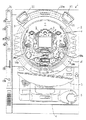
まず、遊技機の一例であるパチンコ遊技機の全体の構成について説明する。図1はパチンコ遊技機1を正面からみた正面図、図2はパチンコ遊技機1の裏面に配置されている各基板を示す背面図、図3はパチンコ遊技機1の機構板を背面からみた背面図である。なお、以下の実施の形態では、パチンコ遊技機を例に説明を行うが、本発明による遊技機はパチンコ遊技機に限られず、画像式の遊技機やスロット機に適用することもできる。
【0026】
図1に示すように、パチンコ遊技機1は、額縁状に形成されたガラス扉枠2を有する。ガラス扉枠2の下部表面には打球供給皿3がある。打球供給皿3の下部には、打球供給皿3からあふれた貯留球を貯留する余剰球受皿4と打球を発射する打球操作ハンドル(操作ノブ)5が設けられている。ガラス扉枠2の後方には、遊技盤6が着脱可能に取り付けられている。また、遊技盤6の前面には遊技領域7が設けられている。
【0027】
遊技領域7の中央付近には、複数種類の図柄を可変表示するための可変表示部9と7セグメントLEDによる可変表示器10とを含む可変表示装置8が設けられている。また、可変表示器10の下部には、4個のLEDからなる通過記憶表示器(普通図柄用記憶表示器)41が設けられている。この実施の形態では、可変表示部9には、「左」、「中」、「右」の3つの図柄表示エリアがある。可変表示装置8の側部には、打球を導く通過ゲート11が設けられている。通過ゲート11を通過した打球は、球出口13を経て始動入賞口14の方に導かれる。通過ゲート11と球出口13との間の通路には、通過ゲート11を通過した打球を検出するゲートスイッチ12がある。また、始動入賞口14に入った入賞球は、遊技盤6の背面に導かれ、始動口スイッチ17によって検出される。また、始動入賞口14の下部には開閉動作を行う可変入賞球装置15が設けられている。可変入賞球装置15は、ソレノイド16によって開状態とされる。
【0028】
可変入賞球装置15の下部には、特定遊技状態(大当り状態)においてソレノイド21によって開状態とされる開閉板20が設けられている。この実施の形態では、開閉板20が大入賞口を開閉する手段となる。開閉板20から遊技盤6の背面に導かれた入賞球のうち一方(Vゾーン)に入った入賞球はVカウントスイッチ22で検出される。また、開閉板20からの入賞球はカウントスイッチ23で検出される。可変表示装置8の下部には、始動入賞口14に入った入賞球数を表示する4個の表示部を有する始動入賞記憶表示器18が設けられている。この例では、4個を上限として、始動入賞がある毎に、始動入賞記憶表示器18は点灯している表示部を1つずつ増やす。そして、可変表示部9の可変表示が開始される毎に、点灯している表示部を1つ減らす。
【0029】
遊技盤6には、複数の入賞口19,24が設けられ、遊技球のそれぞれの入賞口19,24への入賞は、対応して設けられている入賞口スイッチ19a,24aによって検出される。遊技領域7の左右周辺には、遊技中に点滅表示される装飾ランプ25が設けられ、下部には、入賞しなかった打球を吸収するアウト口26がある。また、遊技領域7の外側の左右上部には、効果音を発する2つのスピーカ27が設けられている。遊技領域7の外周には、遊技効果LED28aおよび遊技効果ランプ28b,28cが設けられている。
【0030】
そして、この例では、一方のスピーカ27の近傍に、景品球払出時に点灯する賞球ランプ51が設けられ、他方のスピーカ27の近傍に、補給球が切れたときに点灯する球切れランプ52が設けられている。さらに、図1には、パチンコ遊技台1に隣接して設置され、プリペイドカードが挿入されることによって球貸しを可能にするカードユニット50も示されている。
【0031】
カードユニット50には、使用可能状態であるか否かを示す使用可表示ランプ151、カード内に記録された残額情報に端数(100円未満の数)が存在する場合にその端数を打球供給皿3の近傍に設けられる度数表示LEDに表示させるための端数表示スイッチ152、カードユニット50がいずれの側のパチンコ遊技機1に対応しているのかを示す連結台方向表示器153、カードユニット50内にカードが投入されていることを示すカード投入表示ランプ154、記録媒体としてのカードが挿入されるカード挿入口155、およびカード挿入口155の裏面に設けられているカードリーダライタの機構を点検する場合にカードユニット50を解放するためのカードユニット錠156が設けられている。
【0032】
打球発射装置から発射された打球は、打球レールを通って遊技領域7に入り、その後、遊技領域7を下りてくる。打球が通過ゲート11を通ってゲートスイッチ12で検出されると、可変表示器10の表示数字が連続的に変化する状態になる。また、打球が始動入賞口14に入り始動口スイッチ17で検出されると、図柄の変動を開始できる状態であれば、可変表示部9内の図柄が回転を始める。図柄の変動を開始できる状態でなければ、始動入賞記憶を1増やす。
【0033】
可変表示部9内の画像の回転は、一定時間が経過したときに停止する。停止時の画像の組み合わせが大当り図柄の組み合わせであると、大当り遊技状態に移行する。すなわち、開閉板20が、一定時間経過するまで、または、所定個数(例えば10個)の打球が入賞するまで開放する。そして、開閉板20の開放中に打球が特定入賞領域に入賞しVカウントスイッチ22で検出されると、継続権が発生し開閉板20の開放が再度行われる。継続権の発生は、所定回数(例えば15ラウンド)許容される。
【0034】
停止時の可変表示部9内の画像の組み合わせが確率変動を伴う大当り図柄の組み合わせである場合には、次に大当りとなる確率が高くなる。すなわち、高確率状態という遊技者にとってさらに有利な状態となる。また、可変表示器10における停止図柄が所定の図柄(当り図柄)である場合に、可変入賞球装置15が所定時間だけ開状態になる。さらに、高確率状態では、可変表示器10における停止図柄が当り図柄になる確率が高められるとともに、可変入賞球装置15の開放時間と開放回数が高められる。
【0035】
次に、パチンコ遊技機1の裏面に配置されている各基板について説明する。
図2に示すように、パチンコ遊技機1の裏面では、枠体2A内の機構板の上部に球貯留タンク38が設けられ、パチンコ遊技機1が遊技機設置島に設置された状態でその上方から遊技球が球貯留タンク38に供給される。球貯留タンク38内の遊技球は、誘導樋39を通って球払出機構(図示せず)に至る。
【0036】
遊技機裏面側では、可変表示部9を制御する可変表示制御ユニット29、遊技制御用マイクロコンピュータ等が搭載された遊技制御基板(主基板)31が設置されている。また、球払出制御を行う払出制御用マイクロコンピュータ等が搭載された払出制御基板37、およびモータの回転力を利用して打球を遊技領域7に発射する打球発射装置が設置されている。さらに、装飾ランプ25、遊技効果LED28a、遊技効果ランプ28b,28c、賞球ランプ51および球切れランプ52に信号を送るためのランプ制御基板35、スピーカ27からの音声発生を制御するための音声制御基板70および打球発射装置を制御するための発射制御基板91も設けられている。なお、払出制御基板37には、エラー表示用LED374も搭載されている。
【0037】
さらに、DC30V、DC21V、DC12VおよびDC5Vを作成する電源回路が搭載された電源基板910が設けられ、上方には、各種情報を遊技機外部に出力するための各端子を備えたターミナル基板160が設置されている。ターミナル基板160には、少なくとも、後述する球切れ検出スイッチ167の出力を導入して外部出力するための球切れ用端子、賞球個数信号を外部出力するための賞球用端子および球貸し個数信号を外部出力するための球貸し用端子が設けられている。また、中央付近には、主基板31からの各種情報を遊技機外部に出力するための各端子を備えた情報端子盤(外部情報出力装置)34が設置されている。
【0038】
なお、図2には、ランプ制御基板35および音声制御基板70からの信号を、枠側に設けられている遊技効果LED28a、遊技効果ランプ28b,28c、賞球ランプ51および球切れランプ52に供給するための電飾中継基板A77および度数表示LED等を搭載した残高表示基板74が示されているが、信号中継の必要に応じて他の中継基板も設けられる。
【0039】
また、図3はパチンコ遊技機1の機構板を背面からみた背面図である。球貯留タンク38に貯留された玉は誘導樋39を通り、図3に示すように、球切れ検出器(球切れスイッチ)187a,187bを通過して球供給樋186a,186bを経て球払出装置97に至る。球切れスイッチ187a,187bは遊技球通路内の遊技球の有無を検出するスイッチであるが、球タンク38内の補給球の不足を検出する球切れ検出スイッチ167も設けられている。球払出装置97から払い出された遊技球は、連絡口45を通ってパチンコ遊技機1の前面に設けられている打球供給皿3に供給される。
【0040】
なお、図3には示されていないが、球払出装置97の下方には、球振分部材が設けられている。球振分部材は、振分用ソレノイドによって駆動される。例えば、ソレノイドのオン時には、球振分部材は右側に倒れ、オフ時には左側に倒れる。振分用ソレノイドの下方には、近接スイッチによる賞球カウントスイッチおよび球貸しカウントスイッチが設けられている。すなわち、この実施の形態では、賞球払出も球貸しも同一の球払出装置97によってなされる。ただし、賞球払出を行う機構と球貸しを行う機構とが独立している構成であってもよい。
【0041】
連絡口45の側方には、パチンコ遊技機1の前面に設けられている余剰玉受皿4に連通する余剰玉通路46が形成されている。入賞にもとづく景品球が多数払い出されて打球供給皿3が満杯になり、ついには遊技球が連絡口45に到達した後さらに遊技球が払い出されると遊技球は、余剰玉通路46を経て余剰玉受皿4に導かれる。さらに遊技球が払い出されると、感知レバー47が満タンスイッチ48を押圧して満タンスイッチ48がオンする。その状態では、球払出装置97内のステッピングモータの回転が停止して球払出装置97の動作が停止するとともに打球発射装置34の駆動も停止する。
【0042】
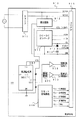
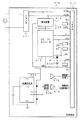
図4は、主基板31における回路構成の一例を示すブロック図である。なお、図4には、払出制御基板37、ランプ制御基板35、音制御基板70、発射制御基板91および表示制御基板80も示されている。主基板31には、プログラムに従ってパチンコ遊技機1を制御する基本回路53と、ゲートスイッチ12、始動口スイッチ17、Vカウントスイッチ22、カウントスイッチ23、入賞口スイッチ19a,24aおよび賞球カウントスイッチ301Aからの信号を基本回路53に与えるスイッチ回路58と、可変入賞球装置15を開閉するソレノイド16および開閉板20を開閉するソレノイド21等を基本回路53からの指令に従って駆動するソレノイド回路59とが搭載されている。
【0043】
また、基本回路53から与えられるデータに従って、大当りの発生を示す大当り情報、可変表示部9の画像表示開始に利用された始動入賞球の個数を示す有効始動情報、確率変動が生じたことを示す確変情報等をホール管理コンピュータ等のホストコンピュータに対して出力する情報出力回路64を含む。
【0044】
基本回路53は、ゲーム制御用のプログラム等を記憶するROM54、ワークメモリとして使用される記憶手段の一例であるRAM55、プログラムに従って制御動作を行うCPU56およびI/Oポート部57を含む。この実施の形態では、ROM54,RAM55はCPU56に内蔵されている。すなわち、CPU56は、1チップマイクロコンピュータである。なお、1チップマイクロコンピュータは、少なくともRAM55が内蔵されていればよく、ROM54およびI/Oポート部57は外付けであっても内蔵されていてもよい。また、RAM55の一部または全部はバックアップ電源でバックアップされているバックアップRAMである。
【0045】
さらに、主基板31には、基本回路53から与えられるアドレス信号をデコードしてI/Oポート部57のうちのいずれかのI/Oポートを選択するための信号を出力するアドレスデコード回路67が設けられている。なお、球払出装置97から主基板31に入力されるスイッチ情報もあるが、図4ではそれらは省略されている。
【0046】
また、CPU56には、電源基板910からリセット信号および電源断信号が供給されている。リセット信号がローレベルであるとCPU56はリセット状態となり、リセット信号がハイレベルになるとCPU56は動作可能状態になる。すなわち、リセット信号は、立ち上がりの時点ではリセット解除信号に相当する。また、電源断信号が、電源電圧が所定値以下になったことを示す状態になると、CPU56は、後述する電源断時処理を実行する。
【0047】
そして、遊技球を打撃して発射する打球発射装置は発射制御基板91上の回路によって制御される駆動モータ94で駆動される。そして、駆動モータ94の駆動力は、操作ノブ5の操作量に従って調整される。すなわち、発射制御基板91上の回路によって、操作ノブ5の操作量に応じた速度で打球が発射されるように制御される。
【0048】
なお、この実施の形態では、ランプ制御基板35に搭載されているランプ制御手段が、遊技盤に設けられている始動記憶表示器18、ゲート通過記憶表示器41および装飾ランプ25の表示制御を行うとともに、枠側に設けられている遊技効果ランプ・LED28a,28b,28c、賞球ランプ51および球切れランプ52の表示制御を行う。ここで、ランプ制御手段は発光体制御手段の一例である。また、特別図柄を可変表示する可変表示部9および普通図柄を可変表示する可変表示器10の表示制御は、表示制御基板80に搭載されている表示制御手段によって行われる。
【0049】
図5は、払出制御基板37および球払出装置97の構成要素などの払出に関連する構成要素を示すブロック図である。図5に示すように、満タンスイッチ48からの検出信号は、中継基板71を介して主基板31のI/Oポート57に入力される。満タンスイッチ48は、余剰球受皿4の満タンを検出するスイッチである。また、球切れスイッチ187a,187bからの検出信号も、中継基板72および中継基板71を介して主基板31のI/Oポート57に入力される。
【0050】
主基板31のCPU56は、球切れスイッチ187a,187bからの検出信号が球切れ状態を示しているか、または、満タンスイッチ48からの検出信号が満タン状態を示していると、払出禁止を指示する払出制御コマンドを送出する。払出禁止を指示する払出制御コマンドを受信すると、払出制御基板37の払出制御用CPU371は球払出処理を停止する。
【0051】
さらに、賞球カウントスイッチ301Aからの検出信号も、中継基板72および中継基板71を介して主基板31のI/Oポート57に入力される。賞球カウントスイッチ301Aは、球払出装置97の下部に設けられ、実際に払い出された賞球払出球を検出する。
【0052】
入賞があると、払出制御基板37には、主基板31の出力ポート(ポート0,1)570,571から賞球個数を示す払出制御コマンドが入力される。出力ポート(出力ポート1)571は8ビットのデータを出力し、出力ポート570は1ビットのストローブ信号(INT信号)を出力する。賞球個数を示す払出制御コマンドは、入力バッファ回路373Aを介してI/Oポート372aに入力される。INT信号は、入力バッファ回路373Bを介して払出制御用CPU371の割込端子に入力されている。払出制御用CPU371は、I/Oポート372aを介して払出制御コマンドを入力し、払出制御コマンドに応じて球払出装置97を駆動して賞球払出を行う。
【0053】
なお、この実施の形態では、払出制御用CPU371は、1チップマイクロコンピュータであり、少なくともRAMが内蔵されている。また、RAMの一部または全部がバックアップ電源でバックアップされているバックアップRAMである。
【0054】
また、主基板31において、出力ポート570,571の外側にバッファ回路620,68Aが設けられている。バッファ回路620,68Aとして、例えば、汎用のCMOS−ICである74HC250,74HC14が用いられる。このような構成によれば、外部から主基板31の内部に入力される信号が阻止されるので、払出制御基板37から主基板31に信号が与えられる可能性がある信号ラインをさらに確実になくすことができる。なお、バッファ回路620,68Aの出力側にノイズフィルタを設けてもよい。
【0055】
払出制御用CPU371は、出力ポート372gおよび情報出力回路377を介して、貸し球数を示す球貸し個数信号をターミナル基板160に出力し、ブザー駆動信号をブザー基板75に出力する。ブザー基板75にはブザーが搭載されている。さらに、出力ポート372eを介して、エラー表示用LED374にエラー信号を出力する。
【0056】
さらに、払出制御基板37の入力ポート372bには、中継基板72を介して、球貸しカウントスイッチ301Bからの検出信号が入力される。球貸しカウントスイッチ301Bは、球払出装置97の下部に設けられ、実際に払い出された貸し球を検出する。払出制御基板37からの払出モータ289への駆動信号は、出力ポート372cおよび中継基板72を介して払出モータ289に伝えられる。払出モータ289の回転に応じて遊技球の払い出しがなされる。
【0057】
球払出装置97の下方には、球振分部材が設けられている。球振分部材は、振分用ソレノイド310によって駆動される。例えば、ソレノイド310のオン時には、球振分部材は右側に倒れ、オフ時には左側に倒れる。振分用ソレノイド310の下方には、近接スイッチによる賞球カウントスイッチ301Aおよび球貸しカウントスイッチ301Bが設けられている。入賞にもとづく賞球時には、球振分部材は右側に倒れ、払い出された遊技球は賞球カウントスイッチ301Aを通過する。また、球貸し時には、球振分部材は左側に倒れ、払い出された遊技球は球貸しカウントスイッチ301Bを通過する。従って、球払出装置97は、賞球時と球貸し時とで払出流下路を切り替えて、所定数の遊技媒体の払出を行うことができる。
【0058】
また、払出制御用CPU371には、電源基板910からリセット信号および電源断信号が供給されている。リセット信号がローレベルであると払出制御用CPU371はリセット状態となり、リセット信号がハイレベルになると払出制御用CPU371は動作可能状態になる。電源断信号が、電源電圧が所定値以下になったことを示す状態になると、払出制御用CPU371は、後述する電源断時処理を実行する。
【0059】
カードユニット50には、カードユニット制御用マイクロコンピュータが搭載されている。また、カードユニット50には、端数表示スイッチ152、連結台方向表示器153、カード投入表示ランプ154およびカード挿入口155が設けられている(図1参照)。残高表示基板74には、打球供給皿3の近傍に設けられている度数表示LED、球貸しスイッチおよび返却スイッチが接続される。
【0060】
残高表示基板74からカードユニット50には、遊技者の操作に応じて、球貸しスイッチ信号および返却スイッチ信号が払出制御基板37を介して与えられる。また、カードユニット50から残高表示基板74には、プリペイドカードの残高を示すカード残高表示信号および球貸し可表示信号が払出制御基板37を介して与えられる。カードユニット50と払出制御基板37の間では、接続信号(VL信号)、ユニット操作信号(BRDY信号)、球貸し要求信号(BRQ信号)、球貸し完了信号(EXS信号)およびパチンコ機動作信号(PRDY信号)がI/Oポート372fを介してやりとりされる。
【0061】
パチンコ遊技機1の電源が投入されると、払出制御基板37の払出制御用CPU371は、カードユニット50にPRDY信号を出力する。また、カードユニット制御用マイクロコンピュータは、VL信号を出力する。払出制御用CPU371は、VL信号の入力状態により接続状態/未接続状態を判定する。カードユニット50においてカードが受け付けられ、球貸しスイッチが操作され球貸しスイッチ信号が入力されると、カードユニット制御用マイクロコンピュータは、払出制御基板37にBRDY信号を出力する。
【0062】
この時点から所定の遅延時間が経過すると、カードユニット制御用マイクロコンピュータは、払出制御基板37にBRQ信号を出力する。そして、払出制御基板37の払出制御用CPU371は、カードユニット50に対するEXS信号を立ち上げ、カードユニット50からのBRQ信号の立ち下がりを検出すると、払出モータ289を駆動し、所定個の貸し球を遊技者に払い出す。このとき、振分用ソレノイド310は駆動状態とされている。すなわち、球振分部材を球貸し側に向ける。そして、払出が完了したら、払出制御用CPU371は、カードユニット50に対するEXS信号を立ち下げる。その後、カードユニット50からのBRDY信号がオン状態でなければ、賞球払出制御を実行する。
【0063】
以上のように、カードユニット50からの信号は、カードユニット50に直接接続されている払出制御基板37に入力される構成になっている。従って、球貸し制御に関して、カードユニット50から主基板31に信号が入力されることはなく、主基板31の基本回路53にカードユニット50の側から不正に信号が入力される余地はない。
【0064】
また、プリペイドカードの残高を示すカード残高表示信号および球貸し可表示信号は、払出制御用CPU371を介さずに残高表示基板74に伝達される。残高表示基板74から送出される球貸しスイッチ信号および返却スイッチ信号も、払出制御用CPU371を介さずにカードユニット50に伝達される。
【0065】
なお、この実施の形態ではカードユニット50が設けられている場合を例にするが、コイン投入に応じてその金額に応じた遊技球を貸し出す場合にも本発明を適用できる。また、この実施の形態では遊技球を貸し出す場合を例にしているが、得点が加算されるものであっても本発明を適用できる。
【0066】
この実施の形態では、少なくとも主基板31および払出制御基板37におけるRAMの一部または全部が、バックアップ電源でバックアップされている。すなわち、遊技機に対する電力供給が停止しても、所定期間はRAMの内容が保存される。そして、各CPUは、電源電圧の低下を検出すると、所定の処理を行った後に電源復旧待ちの状態になる。また、電源投入時に、各CPUは、RAMにデータが保存されている場合には、保存データにもとづいて電源断前の状態を復元する。
【0067】
また、払出制御基板37、表示制御基板80、ランプ制御基板35および音声制御基板70にコマンドを送出するために、主基板31の出力ポート(出力ポート0)570からINT信号が各電気部品制御基板に出力される。この場合、例えば、出力ポート570は8ビット構成であって、ビット0が払出制御基板37へのINT信号、ビット1が表示制御基板80へのINT信号、ビット2がランプ制御基板35へのINT信号、ビット3が音声制御基板70へのINT信号の出力用に用いられる。
【0068】
図6は、表示制御基板80内の回路構成を、可変表示部9の一実現例であるLCD(液晶表示装置)82、可変表示器10、主基板31の出力ポート(ポート0,2)570,572および出力バッファ回路620,62Aとともに示すブロック図である。出力ポート(出力ポート2)572からは8ビットのデータが出力され、出力ポート570からは1ビットのストローブ信号(INT信号)が出力される。
【0069】
表示制御用CPU101には、電源基板910からリセット信号が供給されている。リセット信号がローレベルであると表示制御用CPU101はリセット状態となり、リセット信号がハイレベルになると表示制御用CPU101は動作可能状態になる。
【0070】
表示制御用CPU101は、制御データROM102に格納されたプログラムに従って動作し、主基板31からノイズフィルタ107および入力バッファ回路105Bを介してINT信号が入力されると、入力バッファ回路105Aを介して表示制御コマンドを受信する。入力バッファ回路105A,105Bとして、例えば汎用ICである74HC540,74HC14を使用することができる。なお、表示制御用CPU101がI/Oポートを内蔵していない場合には、入力バッファ回路105A,105Bと表示制御用CPU101との間に、I/Oポートが設けられる。
【0071】
そして、表示制御用CPU101は、受信した表示制御コマンドに従って、LCD82に表示される画面の表示制御を行う。具体的には、表示制御コマンドに応じた指令をVDP103に与える。VDP103は、キャラクタROM86から必要なデータを読み出す。VDP103は、入力したデータに従ってLCD82に表示するための画像データを生成し、R,G,B信号および同期信号をLCD82に出力する。
【0072】
なお、図6には、VDP103をリセットするためのリセット回路83、VDP103に動作クロックを与えるための発振回路85、および使用頻度の高い画像データを格納するキャラクタROM86も示されている。キャラクタROM86に格納される使用頻度の高い画像データとは、例えば、LCD82に表示される人物、動物、または、文字、図形もしくは記号等からなる画像などである。
【0073】
入力バッファ回路105A,105Bは、主基板31から表示制御基板80へ向かう方向にのみ信号を通過させることができる。従って、表示制御基板80側から主基板31側に信号が伝わる余地はない。すなわち、入力バッファ回路105A,105Bは、入力ポートともに不可逆性情報入力手段を構成する。表示制御基板80内の回路に不正改造が加えられても、不正改造によって出力される信号が主基板31側に伝わることはない。
【0074】
なお、出力ポート570,572の出力をそのまま表示制御基板80に出力してもよいが、単方向にのみ信号伝達可能な出力バッファ回路620,62Aを設けることによって、主基板31から表示制御基板80への一方向性の信号伝達をより確実にすることができる。すなわち、出力バッファ回路620,62Aは、出力ポートともに不可逆性情報出力手段を構成する。
【0075】
また、高周波信号を遮断するノイズフィルタ107として、例えば3端子コンデンサやフェライトビーズが使用されるが、ノイズフィルタ107の存在によって、表示制御コマンドに基板間でノイズが乗ったとしても、その影響は除去される。なお、主基板31のバッファ回路620,62Aの出力側にもノイズフィルタを設けてもよい。
【0076】
図7は、主基板31およびランプ制御基板35における信号送受信部分を示すブロック図である。この実施の形態では、遊技領域7の外側に設けられている遊技効果LED28a、遊技効果ランプ28b,28cと遊技盤に設けられている装飾ランプ25の点灯/消灯と、賞球ランプ51および球切れランプ52の点灯/消灯とを示すランプ制御コマンドが主基板31からランプ制御基板35に出力される。また、始動記憶表示器18およびゲート通過記憶表示器41の点灯個数を示すランプ制御コマンドも主基板31からランプ制御基板35に出力される。
【0077】
ランプ制御用CPU351には、電源基板910からリセット信号が供給されている。リセット信号がローレベルであるとランプ制御用CPU351はリセット状態となり、リセット信号がハイレベルになるとランプ制御用CPU351は動作可能状態になる。
【0078】
図7に示すように、ランプ制御に関するランプ制御コマンドは、基本回路53におけるI/Oポート部57の出力ポート(出力ポート0,3)570,573から出力される。出力ポート(出力ポート3)573は8ビットのデータを出力し、出力ポート570は1ビットのINT信号を出力する。ランプ制御基板35において、主基板31からの制御コマンドは、入力バッファ回路355A,355Bを介してランプ制御用CPU351に入力する。なお、ランプ制御用CPU351がI/Oポートを内蔵していない場合には、入力バッファ回路355A,355Bとランプ制御用CPU351との間に、I/Oポートが設けられる。
【0079】
ランプ制御基板35において、ランプ制御用CPU351は、各制御コマンドに応じて定義されている遊技効果LED28a、遊技効果ランプ28b,28c、装飾ランプ25の点灯/消灯パターンに従って、遊技効果LED28a、遊技効果ランプ28b,28c、装飾ランプ25に対して点灯/消灯信号を出力する。点灯/消灯信号は、遊技効果LED28a、遊技効果ランプ28b,28c、装飾ランプ25に出力される。なお、点灯/消灯パターンは、ランプ制御用CPU351の内蔵ROMまたは外付けROMに記憶されている。
【0080】
主基板31において、CPU56は、RAM55の記憶内容に未払出の賞球残数があるときに賞球ランプ51の点灯を指示する制御コマンドを出力し、前述した遊技盤裏面の払出球通路186a,186bの上流に設置されている球切れスイッチ187a,187b(図3参照)が遊技球を検出しなくなると球切れランプ52の点灯を指示する制御コマンドを出力する。ランプ制御基板35において、各制御コマンドは、入力バッファ回路355A,355Bを介してランプ制御用CPU351に入力する。ランプ制御用CPU351は、それらの制御コマンドに応じて、賞球ランプ51および球切れランプ52を点灯/消灯する。なお、点灯/消灯パターンは、ランプ制御用CPU351の内蔵ROMまたは外付けROMに記憶されている。
【0081】
さらに、ランプ制御用CPU351は、制御コマンドに応じて始動記憶表示器18およびゲート通過記憶表示器41に対して点灯/消灯信号を出力する。
【0082】
入力バッファ回路355A,355Bとして、例えば、汎用のCMOS−ICである74HC540,74HC14が用いられる。入力バッファ回路355A,355Bは、主基板31からランプ制御基板35へ向かう方向にのみ信号を通過させることができる。従って、ランプ制御基板35側から主基板31側に信号が伝わる余地はない。たとえ、ランプ制御基板35内の回路に不正改造が加えられても、不正改造によって出力される信号がメイン基板31側に伝わることはない。なお、入力バッファ回路355A,355Bの入力側にノイズフィルタを設けてもよい。
【0083】
また、主基板31において、出力ポート570,573の外側にバッファ回路620,63Aが設けられている。バッファ回路620,63Aとして、例えば、汎用のCMOS−ICである74HC250,74HC14が用いられる。このような構成によれば、外部から主基板31の内部に入力される信号が阻止されるので、ランプ制御基板70から主基板31に信号が与えられる可能性がある信号ラインをさらに確実になくすことができる。なお、バッファ回路620,63Aの出力側にノイズフィルタを設けてもよい。
【0084】
図8は、主基板31における音声制御コマンドの信号送信部分および音声制御基板70の構成例を示すブロック図である。この実施の形態では、遊技進行に応じて、遊技領域7の外側に設けられているスピーカ27の音声出力を指示するための音声制御コマンドが、主基板31から音声制御基板70に出力される。
【0085】
音声制御用CPU701には、電源基板910からリセット信号が供給されている。リセット信号がローレベルであると音声制御用CPU701はリセット状態となり、リセット信号がハイレベルになると音声制御用CPU701は動作可能状態になる。
【0086】
図8に示すように、音声制御コマンドは、基本回路53におけるI/Oポート部57の出力ポート(出力ポート0,4)570,574から出力される。出力ポート(出力ポート4)574からは8ビットのデータが出力され、出力ポート570からは1ビットのINT信号が出力される。音声制御基板70において、主基板31からの各信号は、入力バッファ回路705A,705Bを介して音声制御用CPU701に入力する。なお、音声制御用CPU701がI/Oポートを内蔵していない場合には、入力バッファ回路705A,705Bと音声制御用CPU701との間に、I/Oポートが設けられる。
【0087】
そして、例えばディジタルシグナルプロセッサによる音声合成回路702は、音声制御用CPU701の指示に応じた音声や効果音を発生し音量切替回路703に出力する。音量切替回路703は、音声制御用CPU701の出力レベルを、設定されている音量に応じたレベルにして音量増幅回路704に出力する。音量増幅回路704は、増幅した音声信号をスピーカ27に出力する。
【0088】
入力バッファ回路705A,705Bとして、例えば、汎用のCMOS−ICである74HC540,74HC14が用いられる。入力バッファ回路705A,705Bは、主基板31から音声制御基板70へ向かう方向にのみ信号を通過させることができる。よって、音声制御基板70側から主基板31側に信号が伝わる余地はない。従って、音声制御基板70内の回路に不正改造が加えられても、不正改造によって出力される信号が主基板31側に伝わることはない。なお、入力バッファ回路705A,705Bの入力側にノイズフィルタを設けてもよい。
【0089】
また、主基板31において、出力ポート570,574の外側にバッファ回路620,67Aが設けられている。バッファ回路620,67Aとして、例えば、汎用のCMOS−ICである74HC250,74HC14が用いられる。このような構成によれば、外部から主基板31の内部に入力される信号が阻止されるので、音声制御基板70から主基板31に信号が与えられる可能性がある信号ラインをさらに確実になくすことができる。なお、バッファ回路620,67Aの出力側にノイズフィルタを設けてもよい。
【0090】
図9は、払出制御基板37および打球発射を制御する制御手段が搭載されている発射制御基板91を示すブロック図である。図9に示すように、発射制御信号が、払出制御基板37における出力ポート372dから発射制御基板91に出力される。発射制御基板91において、払出制御基板37からの発射制御信号は、バッファ回路815を介してモータ駆動回路813に入力する。
【0091】
モータ駆動回路813は、例えば、遊技球を発射する球打ち動作および次の遊技球を発射する準備である復旧・球補給動作の各期間における駆動モータ94の回転速度を制御する電圧を発生する。球打ち動作期間では、操作ノブ5に対する回転操作角に対応して徐々に増加する電圧を発生し、復旧・球補給動作期間では、あらかじめ定められた所定の電圧を発生する。
【0092】
タッチセンサ回路93は、操作ノブ5に取り付けられた人体検出用の電極に人体が接触している間、発射許可信号をモータ駆動回路813に出力する。また、モータ駆動回路813には、払出制御基板37からの発射制御信号が与えられる。モータ駆動回路813は、発射制御信号および発射許可信号がオンすると、球打ち動作期間および復旧・球補給動作期間のシーケンス動作の切り替えを制御するとともに、駆動モータ94の駆動に必要な駆動パターン信号および駆動電圧切替信号を発生する。
【0093】
図10は、電源基板910から各基板に供給される直流電圧等を示すブロック図である。図10に示すように、電源基板910には各種直流電圧を生成する電源回路が搭載される。また、必要に応じて、AC24Vも各基板に供給される。
【0094】
この実施の形態では、主基板31には、DC30V、DC12V、DC5Vおよびバックアップ電源電圧(VBB)が供給される。ランプ制御基板35には、DC30V、DC21V、DC12VおよびDC5Vが供給される。払出制御基板37には、AC24V、DC30V、DC12V、DC5Vおよびバックアップ電源電圧(VBB)が供給される。そして、発射制御基板91には、DC30V、DC12VおよびDC5Vが供給される。また、音声制御基板70には、DC12およびDC5Vが供給される。表示制御基板80には、DC12VおよびDC5Vが供給される。さらに、各基板には、電源基板910からリセット信号が供給される。
【0095】
図10に示すように、各基板に供給される電圧のグラウンド側は電源基板910において共通にとられている。従って、各基板におけるグラウンドレベルは共通である。すると、ある基板から他の基板に伝達される信号として、電圧レベルをそのまま使用することができる。グラウンドレベルが共通化されていない基板があると、そのような基板に対する信号伝達を行う場合には、フォトカプラ等の非接触式の情報伝達手段を用いる必要がありコストアップの要因となる。しかし、この実施の形態のように、全ての基板のグラウンドレベルが共通化されている場合には、フォトカプラ等を用いる必要はない。
【0096】
図11は、遊技機の電源基板910の一構成例を示すブロック図である。電源基板910は、主基板31、表示制御基板80、音声制御基板70、ランプ制御基板35および払出制御基板37等の電気部品制御基板と独立して設置され、遊技機内の各電気部品制御基板および機構部品が使用する電圧を生成する。この例では、AC24V、VSL(DC+30V)、DC+21V、DC+12VおよびDC+5Vを生成する。また、バックアップ電源となるコンデンサ916は、DC+5Vすなわち各基板上のIC等を駆動する電源のラインから充電される。
【0097】
トランス911は、交流電源からの交流電圧を24Vに変換する。AC24V電圧は、コネクタ915に出力される。また、整流回路912は、AC24Vから+30Vの直流電圧を生成し、DC−DCコンバータ913およびコネクタ915に出力する。DC−DCコンバータ913は、+21V、+12Vおよび+5Vを生成してコネクタ915に出力する。コネクタ915は例えば中継基板に接続され、中継基板から各電気部品制御基板および機構部品に必要な電圧の電力が供給される。
【0098】
ただし、電源基板910に各電気部品制御基板に至る各コネクタを設け、電源基板910から、中継基板を介さずにそれぞれの基板に至る各電圧を供給するようにしてもよい。
【0099】
DC−DCコンバータ913からの+5Vラインは分岐してバックアップ+5Vラインを形成する。バックアップ+5Vラインとグラウンドレベルとの間には大容量のコンデンサ916が接続されている。コンデンサ916は、遊技機に対する電力供給が遮断されたときの電気部品制御基板のバックアップRAM(電源バックアップされているRAMすなわち記憶内容保持状態となりうる記憶手段)に対して記憶状態を保持できるように電力を供給するバックアップ電源となる。また、+5Vラインとバックアップ+5Vラインとの間に、逆流防止用のダイオード917が挿入される。
【0100】
なお、バックアップ電源として、+5V電源から充電可能な電池を用いてもよい。電池を用いる場合には、+5V電源から電力供給されない状態が所定時間継続すると容量がなくなるような充電池が用いられる。
【0101】
また、電源基板910には、電源監視用IC902が搭載されている。電源監視用IC902は、VSL電源電圧を導入し、VSL電源電圧を監視することによって電源断の発生を検出する。具体的には、VSL電源電圧が所定値(この例では+22V)以下になったら、電源断が生ずるとして電圧低下信号を出力する。なお、監視対象の電源電圧は、各電気部品制御基板に搭載されている回路素子の電源電圧(この例では+5V)よりも高い電圧であることが好ましい。この例では、交流から直流に変換された直後の電圧であるVSLが用いられている。電源監視用IC902からの電圧低下信号は、主基板31や払出制御基板37等に供給される。
【0102】
電源監視用IC902が電源断を検知するための所定値は、通常時の電圧より低いが、各電気部品制御基板上のCPUが暫くの間動作しうる程度の電圧である。また、電源監視用IC902が、CPU等の回路素子を駆動するための電圧(この例では+5V)よりも高く、また、交流から直流に変換された直後の電圧を監視するように構成されているので、CPUが必要とする電圧に対して監視範囲を広げることができる。従って、より精密な監視を行うことができる。
【0103】
さらに、監視電圧としてVSL(+30V)を用いる場合には、遊技機の各種スイッチに供給される電圧が+12Vであることから、電源瞬断時のスイッチオン誤検出の防止も期待できる。すなわち、+30V電源の電圧を監視すると、+30V作成の以降に作られる+12Vが落ち始める以前の段階でそれの低下を検出できる。よって、+12V電源の電圧が低下するとスイッチ出力がオン状態を呈するようになるが、+12Vより早く低下する+30V電源電圧を監視して電源断を認識すれば、スイッチ出力がオン状態を呈する前に電源復旧待ちの状態に入ってスイッチ出力を検出しない状態となることができる。
【0104】
また、電源監視用IC902は、電気部品制御基板とは別個の電源基板910に搭載されているので、電源監視回路から複数の電気部品制御基板に電圧低下信号を供給することができる。電圧低下信号を必要とする電気部品制御基板が幾つあっても第1の電源監視手段は1つ設けられていればよいので、各電気部品制御基板における各電気部品制御手段が後述する復帰制御を行っても、遊技機のコストはさほど上昇しない。
【0105】
なお、図11に示された構成では、電源監視用IC902の検出出力(電圧低下信号)は、バッファ回路918,919を介してそれぞれの電気部品制御基板(例えば主基板31と払出制御基板37)に伝達されるが、例えば、1つの検出出力を中継基板に伝達し、中継基板から各電気部品制御基板に同じ信号を分配する構成でもよい。また、電圧低下信号を必要とする基板数に応じたバッファ回路を設けてもよい。
【0106】
さらに、電源基板910には、各基板にリセット信号を供給するリセット管理回路940が搭載されている。
【0107】
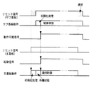
図12は、リセット管理回路940の構成例を示すブロック図である。リセット管理回路940において、リセットIC651は、電源投入時に、外付けのコンデンサの容量で決まる所定時間だけ出力をローレベルとし、所定時間が経過すると出力をハイレベルにする。リセットIC651の出力は、各回路941〜949を介して、バッファ回路961〜964および遅延回路960に供給される。遅延回路960の出力はバッファ回路965に入力する。そして、バッファ回路961〜965が各電気部品制御基板にリセット信号として供給される。従って、リセットIC651の出力がハイレベルになると、各電気部品制御基板におけるCPUが動作可能状態になる。
【0108】
また、リセットIC651は、電源監視用IC902が監視する電源電圧と等しい電源電圧であるVSLの電源電圧を監視して電圧値が所定値(電源監視用IC902が電圧低下信号を出力する電源電圧値よりも低い値)以下になるとローレベルになる。従って、CPU56および払出制御用CPU371は、電源監視用IC902からの電圧低下信号(電源断信号)に応じて所定の電力供給停止準備処理を行った後、システムリセットされることになる。
【0109】
図12に示すように、リセットIC651からのリセット信号は、NAND回路947に入力されるとともに、反転回路(NOT回路)944を介してカウンタIC941のクリア端子に入力される。カウンタIC941は、クリア端子への入力がローレベルになると、発振器943からのクロック信号をカウントする。そして、カウンタIC941のQ5出力がNOT回路945,946を介してNAND回路947に入力される。
【0110】
また、カウンタIC941のQ6出力は、フリップフロップ(FF)942のクロック端子に入力される。フリップフロップ942のD入力はハイレベルに固定され、Q出力は論理和回路(OR回路)949に入力される。OR回路949の他方の入力には、NAND回路947の出力がNOT回路948を介して導入される。そして、OR回路949の出力が、バッファ回路961〜965を介して各CPUに供給されている。このような構成によれば、電源投入時に、各CPUのリセット端子に2回のリセット信号(ローレベル信号)が与えられるので、各CPUは、確実に動作を開始する。
【0111】
そして、例えば、第1の電源監視回路である電源監視用IC902の検出電圧(電圧低下信号を出力することになる電圧)を+22Vとし、第2の電源監視回路に相当するリセットICの検出電圧を+9Vとする。そのように構成した場合には、第1の電源監視回路と第2の電源監視回路とは、同一の電源VSLの電圧を監視するので、第1の電圧監視回路が電圧低下信号を出力するタイミングと第2の電圧監視回路が電圧低下信号を出力するタイミングの差を所望の所定期間に確実に設定することができる。所望の所定期間とは、第1の電源監視回路からの電圧低下信号に応じて電力供給停止準備処理を開始してから電力供給停止準備処理が確実に完了するまでの期間である。
【0112】
この例では、第1の電源監視手段が検出信号を出力することになる第1検出条件は+30V電源電圧が+22Vにまで低下したことであり、第2の電源監視手段が検出信号を出力することになる第2検出条件は+30V電源電圧が+9Vにまで低下したことになる。ただし、ここで用いられている電圧値は一例であって、他の値を用いてもよい。
【0113】
ただし、監視範囲が狭まるが、第1の電圧監視回路および第2の電圧監視回路の監視電圧として+5V電源電圧を用いることも可能である。その場合にも、第1の電圧監視回路の検出電圧は、第2の電圧監視回路の検出電圧よりも高く設定される。
【0114】
主基板31および払出制御基板37のCPU56および払出制御用CPU371の駆動電源である+5V電源から電力が供給されていない間、RAMの少なくとも一部は、電源基板910から供給されるバックアップ電源によってバックアップされ、遊技機に対する電源が断しても内容は保存される。そして、+5V電源が復旧すると、リセット管理回路940からのリセット信号がハイレベルになるので、CPU56および払出制御用CPU371は、通常の動作状態に復帰する。そのとき、必要なデータがバックアップRAMに保存されているので、停電等からの復旧時に停電発生時の遊技状態に復帰することができる。
【0115】
なお、図12では、電源投入時に各電気部品制御基板のCPUのリセット端子に2回のリセット信号(ローレベル信号)が与えられる構成が示されたが、リセット信号の立ち上がりタイミングが1回しかなくても確実にリセット解除されるCPUを使用する場合には、符号941〜949で示された回路素子は不要である。その場合、リセットIC651の出力がそのままバッファ回路961〜964および遅延回路960に接続される。
【0116】
この実施の形態では、電源基板910から各電気部品制御基板のCPUにリセット信号が供給される。また、遅延回路960は、主基板31のCPU56に対するリセット信号を遅延させる。従って、電源投入時に、主基板31のCPU56に対するリセット信号は、他の電気部品制御基板のCPUに対するリセット信号よりも遅く立ち上がる。
【0117】
例えば、主基板31のCPU56が他の電気部品制御基板に対して制御コマンドを出力する際に、他の電気部品制御基板におけるCPUは既に立ち上がっているので、制御コマンドは確実に受信側の電気部品制御基板のCPUで受信される。
【0118】
図13は、リセット管理回路940のリセットIC651とその周辺のICの出力信号の様子を示すタイミング図である。図13に示すように、リセットIC651の出力は、電源電圧のレベルが所定値(各CPUの正常な動作を担保することが可能なレベル、この例では各CPUは+5Vで動作可能なので例えば+9V)を越えるとハイレベルになる。リセットIC651の出力がハイレベルになると、カウンタIC941のクリア状態が解除されるので、カウンタIC941は発振器943の出力クロック信号のカウントを開始する。発振器943の発振周波数は例えば11.776MHzである。
【0119】
カウンタIC941が16クロックをカウントするとQ5出力が立ち上がる。また、32クロックをカウントするとQ6出力がハイレベルに立ち上がる。カウンタIC941のQ6出力が立ち上がると、FF942の出力がハイレベルになる。IC947は、カウンタIC941のQ6出力とリセットIC651の出力との論理積を反転する。OR回路949は、IC947の出力を反転するIC948の出力とFF942の出力との論理和をとって、図13に示すような信号を出力する。
【0120】
バッファ回路961〜964はIC949の出力をそのまま通過させて主基板31のCPU56以外のCPUの対してリセット信号として出力する。また、バッファ回路965は、IC949の出力が遅延された信号を主基板31のCPU56に対してリセット信号として出力する。
【0121】
従って、遊技機の電源オン時には、図13にIC961〜964出力およびIC965出力として示すように、各CPUのリセット端子に対して一旦リセット解除状態(ハイレベル)になってから再度リセット状態(ローレベル)になるような信号が供給される。すなわち、電源オン時には、各CPUをリセット状態とするようなローレベル信号が2回発生することになる。また、リセット解除を示すハイレベルが2回発生しているということもできる。その結果、各CPUは、最初のリセット解除を示すローレベルからハイレベルへの変化によって起動しなかったとしても、2回目のローレベルからハイレベルへの変化によって確実に起動することができる。よって、遊技機の電源投入時に、確実に遊技制御が開始される。
【0122】
図13に示すように、主基板31へのリセット信号がリセット解除状態となるタイミングは、他の基板へのリセット信号がリセット解除状態となるタイミングよりも遅い。従って、主基板31のCPU56が他の電気部品制御基板に対して制御コマンドを出力する際に、他の電気部品制御基板におけるCPUは既に立ち上がっているので、制御コマンドは確実に受信側の電気部品制御基板のCPUで受信される。
【0123】
なお、ここでは、リセット管理回路940が、主基板31に与えられるリセット解除タイミングと他の複数の電気部品制御基板に送られるリセット解除タイミングとをずらせるように制御したが、他の複数の電気部品制御基板に与えられるリセット解除タイミングをそれぞれずらすことも容易である。例えば、図12に示した回路構成において、バッファ回路961〜964の前に遅延回路を置き、各遅延回路の遅延量に差を設ければ、主基板31および他の電気部品制御基板に与えられるリセット解除タイミングのそれぞれの間で差を付けることができる。すなわち、各電気部品制御手段を、あらかじめ定められた順序で立ち上げることができる。
【0124】
各電気部品制御基板のそれぞれにおいて自身が使用するリセット信号を作成するように構成した場合には、それぞれのリセット信号のリセット解除タイミングを調整することが難しいが、この実施の形態では、電源基板910におけるリセット管理回路940が一括して各基板に対するリセット信号を作成するので、立ち上げの順序制御を容易に調整することができる。
【0125】
ただし、各電気部品制御基板のそれぞれにおいて自身が使用するリセット信号を作成するように構成することも可能である。そして、各電気部品制御基板のそれぞれにおいて、リセット解除のタイミングがあらかじめ決められたタイミングになるように各リセット信号作成手段が構成される。例えば、主基板31のリセット信号作成手段が最も遅くリセット解除を行うように、それぞれのタイミング設定がなされる。その場合には、リセット信号の一括管理を行うということはできないが、各電気部品制御基板を、あらかじめ定められた順序で立ち上げることができるという効果は発揮される。
【0126】
なお、この実施の形態では、図12に例示したような立上管理手段が電源基板910に搭載されたが、立上管理手段を搭載した立上管理基板を別個に設けてもよい。ただし、一般にリセット信号は電源電圧の立ち上がりを利用して作成されるので、電源基板910を立上管理基板とした場合には、各リセット信号をより容易に作成できるメリットがある。
【0127】
次に遊技制御動作について説明する。
図14は、主基板31におけるCPU56が実行するメイン処理を示すフローチャートである。遊技機に対する電源が投入されCPU56のリセットが解除されると、メイン処理において、CPU56は、まず、必要な初期設定を行う(ステップS1)。
【0128】
そして、電源断時にバックアップRAM領域のデータ保護処理(例えばパリティデータの付加等の電力供給停止準備処理)が行われたか否か確認する(ステップS2)。この実施の形態では、不測の電源断が生じた場合には、バックアップRAM領域のデータを保護するための電力供給停止準備処理が行われている。そのような処理が行われていた場合をバックアップありとする。バックアップなしを確認したら、CPU56は初期化処理を実行する(ステップS2,S3)。
【0129】
この実施の形態では、バックアップRAM領域にバックアップデータがあるか否かは、電源断時にバックアップRAM領域に設定されるバックアップフラグの状態によって確認される。例えば、バックアップフラグ領域に「55H」が設定されていればバックアップあり(オン状態)を意味し、「55H」以外の値が設定されていればバックアップなし(オフ状態)を意味する。バックアップフラグ領域に設定されている「55H」は、電力供給停止準備処理においてバックアップRAM領域のデータ保護処理が完了したときに設定されたデータであり、バックアップRAM領域のデータにもとづくパリティコードである。
【0130】
バックアップRAM領域にバックアップデータがある場合には、CPU56は、バックアップRAM領域のデータチェック(例えばパリティチェック)を行う(ステップS4)。不測の電源断が生じた後に復旧した場合には、バックアップRAM領域のデータは保存されていたはずであるから、チェック結果は正常になる。チェック結果が正常でない場合には、内部状態を電源断時の状態に戻すことができないので、停電復旧時でない電源投入時に実行される初期化処理を実行する(ステップS5,S3)。
【0131】
チェック結果が正常であれば、CPU56は、内部状態を電源断時の状態に戻すための遊技状態復旧処理を行う(ステップS6)。図15に示すように、バックアップフラグの値が「55H」に設定され、かつ、チェック結果が正常である場合に、ステップS6の遊技状態復旧処理が実行される。そして、バックアップRAM領域に保存されていたPC(プログラムカウンタ)の退避値がPCに設定され、そのアドレスに復帰する(ステップS7)。
【0132】
通常の初期化処理の実行(ステップS3)が完了すると、メイン処理で、タイマ割込フラグの監視(ステップS9)の確認が行われるループ処理に移行する。なお、ループ内では、表示用乱数更新処理(ステップS8)も実行される。
【0133】
なお、この実施の形態では、ステップS2でバックアップデータの有無が確認された後、バックアップデータが存在する場合にステップS4でバックアップ領域のチェックが行われたが、逆に、バックアップ領域のチェック結果が正常であったことが確認された後、バックアップデータの有無の確認を行うようにしてもよい。また、バックアップデータの有無の確認、またはバックアップ領域のチェックの何れか一方の確認を行うことによって、停電復旧処理を実行するか否かを判定してもよい。
【0134】
また、例えば停電復旧処理を実行するか否か判断する場合のパリティチェック(ステップS4)の際に、すなわち、遊技状態を復旧するか否か判断する際に、保存されていたRAMデータにおける特別プロセスフラグ等や始動入賞記憶数データによって、遊技機が遊技待機状態(図柄変動中でなく、大当り遊技中でなく、確変中でなく、また、始動入賞記憶がない状態)であることが確認されたら、遊技状態復旧処理を行わずに初期化処理を実行するようにしてもよい。
【0135】
図16は、ステップS1の初期設定処理を示すフローチャートである。初期設定処理において、CPU56は、まず、割込禁止に設定する(ステップS1a)。割込禁止に設定すると、CPU56は、割込モードを割込モード2に設定し(ステップS1b)、スタックポインタにスタックポインタ指定アドレスを設定する(ステップS1c)。そして、CPU56は、内蔵デバイスレジスタの初期化を行う(ステップS1d)。また、内蔵デバイス(内蔵周辺回路)であるCTC(カウンタ/タイマ)およびPIO(パラレル入出力ポート)の初期化(ステップS1e)を行った後、RAMをアクセス可能状態に設定する(ステップS1f)。
【0136】
この実施の形態で用いられているCPU56には、マスク可能な割込(INT)のモードとして以下の3種類のモードが用意されている。そのうちの割込モード2に設定されると、各内蔵デバイスからの割込要求を容易に処理することが可能になり、また、プログラムにおける任意の位置に割込処理を設置することが可能になる。なお、マスク可能な割込が発生すると、CPU56は、自動的に割込禁止状態に設定するとともに、プログラムカウンタの内容をスタックにセーブする。
【0137】
図17は、通常の初期化処理(ステップS3)の処理を示すフローチャートである。図17に示すように、初期化処理では、RAMのクリア処理が行われる(ステップS3a)。次いで、作業領域初期設定テーブルのアドレス値にもとづいて、所定の作業領域(例えば、普通図柄判定用乱数カウンタ、普通図柄判定用バッファ、特別図柄左中右図柄バッファ、払出コマンド格納ポインタなど)に初期値を設定する初期値設定処理(ステップS3b)が行われる。
【0138】
そして、2ms毎に定期的にタイマ割込がかかるようにCPU56に設けられているCTCのレジスタの設定が行われる(ステップS3c)。すなわち、初期値として2msに相当する値が所定のレジスタ(時間定数レジスタ)に設定される。そして、初期設定処理(ステップS1)において割込禁止(図16参照)にされているので、初期化処理を終える前に割込が許可される(ステップS3d)。
【0139】
従って、この実施の形態では、CPU56の内蔵CTCが繰り返しタイマ割込を発生するように設定される。この実施の形態では、繰り返し周期は2msに設定される。そして、図18に示すように、タイマ割込が発生すると、CPU56は、タイマ割込フラグをセットする(ステップS12)。
【0140】
CPU56は、ステップS9において、タイマ割込フラグがセットされたことを検出すると、タイマ割込フラグをリセットするとともに(ステップS10)、遊技制御処理を実行する(ステップS11)。以上の制御によって、この実施の形態では、遊技制御処理は2ms毎に起動されることになる。なお、この実施の形態では、タイマ割込処理ではフラグセットのみがなされ、遊技制御処理はメイン処理において実行されるが、タイマ割込処理で遊技制御処理を実行してもよい。
【0141】
図19は、ステップS11の遊技制御処理を示すフローチャートである。遊技制御処理において、CPU56は、まず、スイッチ回路58を介して、ゲートセンサ12、始動口センサ17、カウントセンサ23および入賞口スイッチ19a,24aの状態を入力し、各入賞口や入賞装置に対する入賞があったか否か判定する(スイッチ処理:ステップS21)。
【0142】
次いで、パチンコ遊技機1の内部に備えられている自己診断機能によって種々の異常診断処理が行われ、その結果に応じて必要ならば警報が発せられる(エラー処理:ステップS22)。
【0143】
次に、遊技制御に用いられる大当り判定用の乱数等の各判定用乱数を示す各カウンタを更新する処理を行う(ステップS23)。CPU56は、さらに、停止図柄の種類を決定する乱数等の表示用乱数を更新する処理を行う(ステップS24)。
【0144】
さらに、CPU56は、特別図柄プロセス処理を行う(ステップS25)。特別図柄プロセス制御では、遊技状態に応じてパチンコ遊技機1を所定の順序で制御するための特別図柄プロセスフラグに従って該当する処理が選び出されて実行される。そして、特別図柄プロセスフラグの値は、遊技状態に応じて各処理中に更新される。
【0145】
また、普通図柄プロセス処理を行う(ステップS26)。普通図柄プロセス処理では、7セグメントLEDによる可変表示器10を所定の順序で制御するための普通図柄プロセスフラグに従って該当する処理が選び出されて実行される。そして、普通図柄プロセスフラグの値は、遊技状態に応じて各処理中に更新される。
【0146】
さらに、CPU56は、払出制御基板37等に送出される制御コマンドをRAM55の所定の領域に設定して各電気部品制御基板に対して制御コマンドを送出する処理を行う(コマンド制御処理:ステップS27)。
【0147】
次いで、CPU56は、例えばホール管理用コンピュータに供給される大当り情報、始動情報、確率変動情報などのデータを出力するデータ出力処理を行う(ステップS29)。
【0148】
また、CPU56は、所定の条件が成立したときにソレノイド回路59に駆動指令を行う(ステップS30)。ソレノイド回路59は、駆動指令に応じてソレノイド16,21を駆動し、可変入賞球装置15または開閉板20を開状態または閉状態とする。
【0149】
そして、CPU56は、各入賞口への入賞を検出するためのスイッチ17,23,19a,24aの検出出力にもとづく賞球数の設定などを行う(ステップS31)。具体的には、入賞検出に応じて払出制御基板37に払出制御コマンドを出力する。払出制御基板37に搭載されている払出制御用CPU371は、払出制御コマンドに応じて賞球払出装置97Aを駆動する。
【0150】
以上のように、メイン処理には遊技制御処理に移行すべきか否かを判定する処理が含まれ、CPU56の内部タイマが定期的に発生するタイマ割込にもとづくタイマ割込処理で遊技制御処理に移行すべきか否かを判定するためのフラグがセットされるので、遊技制御処理の全てが確実に実行される。つまり、遊技制御処理の全てが実行されるまでは、次回の遊技制御処理に移行すべきか否かの判定が行われないので、遊技制御処理中の全ての各処理が実行完了することは保証されている。
【0151】
なお、ここでは、主基板31のCPU56が実行する遊技制御処理は、CPU56の内部タイマが定期的に発生するタイマ割込にもとづくタイマ割込処理でセットされるフラグに応じて実行されたが、定期的に(例えば2ms毎)信号を発生するハードウェア回路を設け、その回路からの信号をCPU56の外部割込端子に導入し、割込信号によって遊技制御処理に移行すべきか否かを判定するためのフラグをセットするようにしてもよい。
【0152】
図20は、電源基板910からの電源断信号にもとづくNMIに応じて実行される停電発生NMI処理の一例を示すフローチャートである。停電発生NMI処理において、CPU56は、まず、停電時などの電源断時直前の割込許可/禁止状態をバックアップするために、割込禁止フラグの内容をパリティフラグに格納する(ステップS41)。
【0153】
次いで、割込禁止に設定する(ステップS42)。停電発生NMI処理ではRAM内容の保存を確実にするためにチェックサムの生成処理を行う。その処理中に他の割込処理が行われたのではチェックサムの生成処理が完了しないうちにCPUが動作し得ない電圧にまで低下してしまうことが考えられるので、まず、他の割込が生じないような設定がなされる。なお、停電発生NMI処理におけるステップS44〜S50は、電力供給停止準備処理の一例である。また、割込処理中では他の割込がかからないような仕様のCPUを用いている場合には、ステップS42の処理は不要である。
【0154】
次いで、CPU56は、バックアップフラグが既にセットされているか否か確認する(ステップS42)。バックアップフラグが既にセットされていれば、以後の処理を行わない。バックアップフラグがセットされていなければ、以下の電力供給停止準備処理を実行する。すなわち、ステップS44からステップS50の処理を実行する。
【0155】
まず、各レジスタの内容をバックアップRAM領域に格納する(ステップS44)。その後、バックアップフラグをセットする(ステップS45)。そして、バックアップRAM領域のバックアップチェックデータ領域に適当な初期値を設定し(ステップS46)、初期値およびバックアップRAM領域のデータについて順次排他的論理和をとったあと反転し(ステップS47)、最終的な演算値をバックアップパリティデータ領域に設定する(ステップS48)。また、RAMアクセス禁止状態にする(ステップS49)。電源電圧が低下していくときには、各種信号線のレベルが不安定になってRAM内容が化ける可能性があるが、このようにRAMアクセス禁止状態にしておけば、バックアップRAM内のデータが化けることはない。
【0156】
さらに、CPU56は、主基板31に搭載されている全ての出力ポートに対してクリア信号を出力する。すると、全ての出力ポートは、クリア信号によりクリアされオフ状態とされる(ステップS50)。
【0157】
次いで、CPU56は、ループ処理にはいる。すなわち、何らの処理もしない状態になる。従って、リセット管理回路940からのリセット信号がローレベルになって動作禁止状態にされる前に、内部的に動作停止状態になる。よって、電源断時に確実にCPU56は動作停止する。その結果、上述したRAMアクセス禁止の制御および動作停止制御によって、電源電圧が低下していくことに伴って生ずる可能性がある異常動作に起因するRAMの内容破壊等を確実に防止することができる。
【0158】
なお、この実施の形態では、停電発生NMI処理では最終部でプログラムをループ状態にしたが、ホールト(HALT)命令を発行するように構成してもよい。
【0159】
また、レジスタの内容をRAM領域に格納した後にセットされるバックアップフラグは、上述したように、電源投入時において復旧すべきバックアップデータがあるか否か(停電からの復旧か否か)を判断する際に使用される。また、ステップS41からS50の処理は、CPU56がシステムリセット回路65からのシステムリセット信号を受ける前に完了する。換言すれば、システムリセット回路65からのシステムリセット信号を受ける前に完了するように、電圧監視回路の検出電圧の設定が行われている。
【0160】
この実施の形態では、電力供給停止準備処理開始時に、バックアップフラグの確認が行われる。そして、バックアップフラグが既にセットされている場合には電力供給停止準備処理を実行しない。上述したように、バックアップフラグは、必要なデータのバックアップが完了し、その後電力供給停止準備処理が完了したことを示すフラグである。従って、例えば、リセット待ちのループ状態で何らかの原因で再度NMIが発生したとしても、電力供給停止準備処理が重複して実行されてしまうようなことはない。
【0161】
ただし、割込処理中では他の割込がかからないような仕様のCPUを用いている場合には、ステップS43の判断は不要である。
【0162】
図21は、バックアップパリティデータ作成方法の一例を説明するための説明図である。ただし、図21に示す例では、簡単のために、バックアップデータRAM領域のデータのサイズを3バイトとする。電源電圧低下にもとづく停電発生処理において、図21に示すように、バックアップチェックデータ領域に、初期データ(この例では00H)が設定される。次に、「00H」と「F0H」の排他的論理和がとられ、その結果と「16H」の排他的論理和がとられる。さらに、その結果と「DFH」の排他的論理和がとられる。そして、その結果(この例では「39H」)を反転して得られた値(この例では「C6H」)がバックアップパリティデータ領域に設定される。
【0163】
電源が再投入されたときには、停電復旧処理においてパリティ診断が行われる。バックアップ領域の全データがそのまま保存されていれば、電源再投入時に、図21に示すようなデータがバックアップ領域に設定されている。
【0164】
ステップS4の処理において、CPU56は、電源発生MNI処理にて実行された処理と同様の処理を行う。すなわち、バックアップチェックデータ領域に、初期データ(この例では00H)が設定され、「00H」と「F0H」の排他的論理和がとられ、その結果と「16H」の排他的論理和がとられる。さらに、その結果と「DFH」の排他的論理和がとられる。そして、その結果(この例では「39H」)を反転した最終演算結果を得る。バックアップ領域の全データがそのまま保存されていれば、最終的な演算結果は、「C6H」、すなわちバックアップチェックデータ領域に設定されているデータと一致する。バックアップRAM領域内のデータにビット誤りが生じていた場合には、最終的な演算結果は「C6H」にならない。
【0165】
よって、CPU56は、最終的な演算結果とバックアップチェックデータ領域に設定されているデータとを比較して、一致すればパリティ診断正常とする。一致しなければ、パリティ診断異常とする。
【0166】
以上のように、この実施の形態では、遊技制御手段には、遊技機の電源が断しても、所定期間電源バックアップされる記憶手段(この例ではバックアップRAM)が設けられ、電源投入時に、CPU56(具体的にはCPU56が実行するプログラム)は、記憶手段がバックアップ状態にあればバックアップデータにもとづいて遊技状態を回復させる遊技状態復旧処理(ステップS6)を行うように構成される。
【0167】
なお、この実施の形態では、電源基板910において、電源監視用IC902と、リセット管理回路940は、同一の電源電圧を監視しているが、異なる電源電圧を監視してもよい。例えば、電源監視用IC902が+30V電源電圧を監視し、リセット管理回路940が+5V電源電圧を監視してもよい。そして、リセット管理回路940がリセット信号をローレベルにするタイミングは電源監視用IC902がNMI割込信号(電源断信号)を発生するタイミングに対して遅くなるように、システムリセット回路65のしきい値レベル(システムリセット信号を発生する電圧レベル)が設定される。例えば、しきい値は4.25Vである。4.25Vは、通常時の電圧より低いが、CPU56が暫くの間動作しうる程度の電圧である。
【0168】
また、上記の実施の形態では、CPU56は、マスク不能割込端子(NMI端子)を介して電源基板からのNMI割込信号(電源監視手段からのNMI割込信号)を検知したが、NMI割込信号をマスク可能割込割込端子(IRQ端子)に導入してもよい。その場合には、割込処理(IRQ処理)で電力供給停止準備処理が実行される。また、入力ポートを介して電源基板からのNMI割込信号を検知してもよい。その場合には、メイン処理において入力ポートの監視が行われる。
【0169】
また、NMI割込信号に変えて、IRQ端子を介して電源基板からの割込信号を検知する場合に、メイン処理のステップS11における遊技制御処理の開始時にIRQ割込マスクをセットし、遊技制御処理の終了時にIRQ割込マスクを解除するようにしてもよい。そのようにすれば、遊技制御処理の開始前および終了後に割込がかかることになって、遊技制御処理が中途で中断されることはない。従って、払出制御コマンドを払出制御基板37に送出しているときなどにコマンド送出が中断されてしまうようなことはない。よって、停電が発生するようなときでも、払出制御コマンド等は確実に送出完了する。
【0170】
図22は、払出制御用CPU371のメイン処理を示すフローチャートである。メイン処理では、払出制御用CPU371は、まず、必要な初期設定を行う(ステップS701)。
【0171】
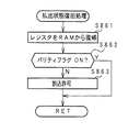
そして、払出制御用CPU371は、払出制御用のバックアップRAM領域にバックアップデータが存在しているか否かの確認を行う(ステップS702)。すなわち、例えば、主基板31のCPU56の処理と同様に、電源断時にセットされるバックアップフラグがセット状態になっているか否かによって、バックアップデータが存在しているか否か確認する。バックアップフラグがセット状態になっている場合には、バックアップデータありと判断する。バックアップデータなしと判断された場合には、前回の電源オフ時に未払出の遊技球がなかったことになり、内部状態を電源断時の状態に戻す必要がない。従って、払出制御用CPU371は、停電復旧時でない電源投入時に実行される初期化処理を実行する(ステップS702,S703)。
【0172】
バックアップRAM領域にバックアップデータが存在している場合には、払出制御用CPU371は、バックアップRAM領域のデータチェック(この例ではパリティチェック)を行う(ステップS704)。不測の電源断が生じた後に復旧した場合には、バックアップRAM領域のデータは保存されていたはずであるから、チェック結果は正常になる。チェック結果が正常でない場合には、内部状態を電源断時の状態に戻すことができないので、停電復旧時でない電源投入時に実行される初期化処理を実行する(ステップS705,S703)。
【0173】
チェック結果が正常であれば、払出制御用CPU371は、内部状態を電源断時の状態に戻すための払出状態復旧処理を行う(ステップS706)。そして、バックアップRAM領域に保存されていたPC(プログラムカウンタ)の指すアドレスに復帰する(ステップS707)。
【0174】
通常の初期化処理の実行(ステップS703)を終えると、払出制御用CPU371により実行されるメイン処理は、タイマ割込フラグの監視(ステップS708)の確認が行われるループ処理に移行する。
【0175】
なお、この実施の形態では、ステップS702でバックアップデータの有無が確認された後、バックアップデータが存在する場合にステップS704でバックアップ領域のチェックが行われたが、逆に、バックアップ領域のチェック結果が正常であったことが確認された後に、バックアップデータの有無の確認が行われるようにしてもよい。また、バックアップデータの有無の確認、またはバックアップ領域のチェックの何れか一方を確認することによって、停電復旧処理を実行するか否かを判断するように構成してもよい。
【0176】
また、例えば停電復旧処理を実行するか否か判断する場合のパリティチェック(ステップS704)の際などに、すなわち、遊技状態を復旧するか否か判断する際に、保存されていたRAMデータにおける払出遊技球数データ等によって、遊技機が払出待機状態(払出途中でない状態)であることが確認されたら、払出状態復旧処理を行わずに初期化処理を実行するようにしてもよい。
【0177】
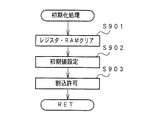
通常の初期化処理では、図23に示すように、レジスタおよびRAMのクリア処理(ステップS901)が行われ、所定の初期値の設定が行われる(ステップS902)。そして、初期化処理を終える前に割込が許可される(ステップS903)。
【0178】
この実施の形態では、払出制御用CPU371の内蔵タイマ/カウンタが繰り返しタイマ割込を発生するように設定される。また、繰り返し周期は2msに設定される。そして、図24に示すように、タイマ割込が発生すると、払出制御用CPU371は、タイマ割込フラグをセットする(ステップS711)。なお、図24には割込を許可することも明示されているが(ステップS710)、2msタイマ割込処理では、最初に割込許可状態に設定される。すなわち、2msタイマ割込処理中には割込許可状態になっている。
【0179】
払出制御用CPU371は、ステップS708において、タイマ割込フラグがセットされたことを検出すると、タイマ割込フラグをリセットするとともに(ステップS709)、払出制御処理を実行する(ステップS710)。以上の制御によって、この実施の形態では、払出制御処理は2ms毎に起動されることになる。なお、この実施の形態では、タイマ割込処理ではフラグセットのみがなされ、払出制御処理はメイン処理において実行されるが、タイマ割込処理で払出制御処理を実行してもよい。
【0180】
払出制御用CPU371は、電源投入時に、バックアップRAM領域のデータを確認するだけで、通常の初期設定処理を行うのか払出中の状態を復元するのか決定できる。すなわち、簡単な判断によって、未払出の遊技球について払出処理再開を行うことができる。さらに、この実施の形態では、主基板31における遊技制御と同様に、パリティチェックコードによって記憶内容保存の確実化が図られている。
【0181】
図25は、ステップS710の払出制御処理を示すフローチャートである。払出制御処理において、払出制御用CPU371は、まず、中継基板72を介して入力ポート372bに入力される賞球カウントスイッチ301A、球貸しカウントスイッチ301Bがオンしたか否かを判定する(スイッチ処理:ステップS751)。
【0182】
次に、払出制御用CPU371は、センサ(例えば、払出モータ289の回転数を検出するモータ位置センサ)からの信号入力状態を確認してセンサの状態を判定する等の処理を行う(入力判定処理:ステップS752)。払出制御用CPU371は、さらに、受信した払出制御コマンドを解析し、解析結果に応じた処理を実行する(コマンド解析実行処理:ステップS753)。
【0183】
次いで、払出制御用CPU371は、主基板31から払出停止指示コマンドを受信していたら払出停止状態に設定し、払出開始指示コマンドを受信していたら払出停止状態の解除を行う(ステップS754)。また、プリペイドカードユニット制御処理を行う(ステップS755)。
【0184】
また、払出制御用CPU371は、球貸し要求に応じて貸し球を払い出す制御を行う(ステップS756)。さらに、払出制御用CPU371は、所定の賞球を払い出す賞球制御処理を行う(ステップS757)。そして、払出制御用CPU371は、出力ポート372cおよび中継基板72を介して球払出装置97の払出機構部分における払出モータ289に向けて駆動信号を出力し、ステップS756の球貸し制御処理またはステップS757の賞球制御処理で設定された回転数分払出モータ289を回転させる払出モータ制御処理を行う(ステップS758)。
【0185】
なお、この実施の形態では、払出モータ289としてステッピングモータが用いられ、払出モータ289を制御するために1−2相励磁方式が用いられる。従って、具体的には、払出モータ制御処理において、8種類の励磁パターンデータが繰り返し払出モータ289に出力される。また、この実施の形態では、各励磁パターンデータが4msずつ出力される。
【0186】
次いで、エラー検出処理が行われ、その結果に応じてエラー表示LED374に所定の表示を行う(エラー処理:ステップS759)。
【0187】
さらに、ターミナル基板160に情報信号を出力する処理を行う(出力処理:ステップS760)。なお、情報信号は、貸し球の払出一単位(例えば25個)ごとに所定時間オンとなり、続いて所定時間オフを出力する信号である。
【0188】
図26は、電源基板910の電源監視用IC902からの電源断信号にもとづくNMIに応じて実行される停電発生NMI処理の一例を示すフローチャートである。停電発生NMI処理において、払出制御用CPU371は、まず、割込禁止フラグの内容をパリティフラグに格納する(ステップS801)。次いで、割込禁止に設定する(ステップS802)。
【0189】
停電発生NMI処理では、主基板31において実行された処理と同様に、RAM内容の保存を確実にするためのチェックサムの生成処理を行う。その処理中に他の割込処理が行われたのではチェックサムの生成処理が完了しないうちに払出制御用CPU371が動作し得ない電圧にまで低下してしまうことがことも考えられるので、まず、他の割込が生じないような設定がなされる。なお、停電発生NMI処理におけるステップS804〜S810は、電力供給停止準備処理の一例である。
【0190】
なお、割込処理中では他の割込がかからないような仕様のCPUを用いている場合には、ステップS802の処理は不要である。
【0191】
次いで、払出制御用CPU371は、バックアップフラグが既にセットされているか否か確認する(ステップS803)。バックアップフラグが既にセットされていれば、以後の処理を行わない。バックアップフラグがセットされていなければ、以下の電力供給停止準備処理を実行する。すなわち、ステップS804からステップS810の処理を実行する。
【0192】
まず、各レジスタの内容をバックアップRAM領域に格納する(ステップS804)。その後、バックアップフラグをセットする(ステップS805)。そして、バックアップRAM領域のバックアップチェックデータ領域に適当な初期値を設定し(ステップS806)、初期値およびバックアップRAM領域のデータについて順次排他的論理和をとったあと反転し(ステップS807)、最終的な演算値をバックアップパリティデータ領域に設定する(ステップS808)。また、RAMアクセス禁止状態にする(ステップS809)。電源電圧が低下していくときには、各種信号線のレベルが不安定になってRAM内容が化ける可能性があるが、このようにRAMアクセス禁止状態にしておけば、バックアップRAM内のデータが化けることはない。
【0193】
さらに、払出制御用CPU371は、全ての出力ポートに対してクリア信号を出力する。従って、全ての出力ポートは、クリア信号によりオフ状態とされる(ステップS810)。
【0194】
次いで、払出制御用CPU371は、ループ処理にはいる。すなわち、何らの処理もしない状態になる。従って、リセット管理回路940からのリセット信号がローレベルになって動作禁止状態にされる前に、内部的に動作停止状態になる。よって、電源断時に確実に払出制御用CPU371は動作停止する。その結果、上述したRAMアクセス禁止の制御および動作停止制御によって、電源電圧が低下していくことに伴って生ずる可能性がある異常動作に起因するRAMの内容破壊等を確実に防止することができる。
【0195】
なお、この実施の形態では、停電発生NMI処理では最終部でプログラムをループ状態にしたが、ホールト(HALT)命令を発行するように構成してもよい。
【0196】
また、レジスタの内容をRAM領域に格納した後にセットされるバックアップフラグは、上述したように、電源投入時において復旧すべきバックアップデータがあるか否か(停電からの復旧か否か)を判断する際に使用される。また、ステップS801からS810の処理は、払出制御用CPU371が電源基板910からのリセット信号がローレベルになる前に完了する。換言すれば、電源基板910からのリセット信号がリセット状態を示すようになる前に完了するように、電源基板910の電圧監視用IC902において検出電圧の設定が行われている。
【0197】
この実施の形態では、電力供給停止準備処理開始時に、バックアップフラグの確認が行われる。そして、バックアップフラグが既にセットされている場合には電力供給停止準備処理を実行しない。上述したように、バックアップフラグは、必要なデータのバックアップが完了し、その後電力供給停止準備処理が完了したことを示すフラグである。従って、例えば、リセット待ちのループ状態で何らかの原因で再度NMIが発生したとしても、電力供給停止準備処理が重複して実行されてしまうようなことはない。
【0198】
ただし、割込処理中では他の割込がかからないような仕様のCPUを用いている場合には、ステップS803の判断は不要である。
【0199】
また、この実施の形態では、払出制御用CPU371は、マスク不能外部割込端子(NMI端子)を介して電源基板からのNMI割込信号(電源監視手段からのNMI割込信号)を検知したが、NMI割込信号をマスク可能割込割込端子(IRQ端子)に導入してもよい。その場合には、IRQ処理によって図26に示された停電発生NMI処理が実行される。また、入力ポートを介してNMI割込信号を検知してもよい。その場合には、払出制御用CPU371が実行するメイン処理において、入力ポートの監視が行われる。
【0200】
図27は、バックアップパリティデータ作成方法の一例を説明するための説明図である。ただし、図27に示す例では、簡単のために、バックアップデータRAM領域のデータのサイズを3バイトとする。電源電圧低下にもとづく停電発生処理において、図27に示すように、バックアップチェックデータ領域に、初期データ(この例では00H)が設定される。次に、「00H」と「F0H」の排他的論理和がとられ、その結果と「16H」の排他的論理和がとられる。さらに、その結果と「DFH」の排他的論理和がとられる。そして、その結果(この例では「39H」)を反転して得られた値(この例では「C6H」)がバックアップパリティデータ領域に設定される。
【0201】
電源が再投入されたときには、停電復旧処理においてパリティ診断が行われる。バックアップ領域の全データがそのまま保存されていれば、電源再投入時に、図27に示すようなデータがバックアップ領域に設定されている。
【0202】
ステップS704の処理において、払出制御用CPU371は、図26のステップS806およびステップS807にて実行された処理と同様の処理を行う。すなわち、バックアップチェックデータ領域に、初期データ(この例では00H)が設定され、「00H」と「F0H」の排他的論理和がとられ、その結果と「16H」の排他的論理和がとられる。さらに、その結果と「DFH」の排他的論理和がとられる。そして、その結果(この例では「39H」)を反転した最終演算結果を得る。バックアップ領域の全データがそのまま保存されていれば、最終的な演算結果は、「C6H」、すなわちバックアップチェックデータ領域に設定されているデータと一致する。バックアップRAM領域内のデータにビット誤りが生じていた場合には、最終的な演算結果は「C6H」にならない。
【0203】
よって、払出制御用CPU371は、最終的な演算結果とバックアップチェックデータ領域に設定されているデータとを比較して、一致すればパリティ診断正常とする。一致しなければ、パリティ診断異常とする。
【0204】
以下、払出状態復旧処理について説明する。図28は、図22のステップS706に示された払出状態復旧処理の一例を示すフローチャートである。この例では、払出制御用CPU371は、バックアップRAMに保存されていた値をレジスタに復元する(ステップS861)。そして、バックアップRAMに保存されていたデータにもとづいて停電時の払出状態を復旧するための処理を行う。例えば、賞球中処理中フラグのセット等を行う。
【0205】
例えば、電源復旧時に、バックアップRAM領域に、未払出賞球数もしくは未払出貸し球数、またはそれらの両方が保存されていた場合には、それらの保存数にもとづいて払出処理を再開する。
【0206】
以上のように、この実施の形態では、払出制御手段には、遊技機の電源が断しても、所定期間電源バックアップされる記憶手段(この例ではバックアップRAM)が設けられ、電源投入時に、払出制御用CPU371(具体的には払出制御用CPU371が実行するプログラム)は、記憶手段がバックアップ状態にあればバックアップデータにもとづいて払出状態を回復させる払出状態復旧処理(ステップS706)を行うように構成される。
【0207】
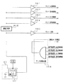
図11に例示した電源基板910の構成において、電源監視用IC902が出力する信号は、バッファ回路918を介して主基板31に対して電源断信号として出力されるとともに、遅延回路920およびバッファ回路919を介して払出制御基板37に対して電源断信号として出力されていた。すると、図29に示すように、遊技機の電源が断する際に、主基板31のCPU56には、払出制御基板37の払出制御用CPU371に対するよりも早く電源断信号が供給される。
【0208】
従って、図29に示すように、主基板31のCPU56には、払出制御基板37の払出制御用CPU371よりも早くNMIがかかる。NMIに応じて電力供給停止準備処理が開始されるので、その時点で、CPU56による遊技制御および払出制御用CPU371による払出制御は停止する。
【0209】
すなわち、電源基板910に搭載されている立下管理手段が、遊技制御手段を立ち下げた後に払出制御手段(価値付与制御手段)を立ち下げるという順序制御を行っている。従って、主基板31のCPU56が他の電気部品制御基板に対して制御コマンドを出力する前に、払出制御手段におけるCPUが既に立ち下がっていることはなく、主基板31からの制御コマンドが受信側の電気部品制御基板のCPUで受信されないという事態は生じない。なお、この実施の形態では、立下管理手段は、電源監視用IC902、制御手段の作動を停止させるためのリセット信号を出力可能なリセット管理回路940および遅延回路920で実現されている。
【0210】
ここでは、立下管理手段が、主基板31に与えられる電源断信号と払出制御手段に送られる電源断信号とのタイミングをずらせることによって、それらの間の立ち下げの順序制御を行ったが、他の複数の電気部品制御基板、例えば表示制御基板70、ランプ制御基板35および音声制御基板80等の遊技演出に関わる電気部品制御手段を搭載した電気部品制御基板の立ち下げタイミングを制御することもできる。例えば、図12に示した回路構成において、主基板31および払出制御基板371以外の電気部品制御基板に対してもバッファ回路を介して電源断信号を出力するようにすればよい。
【0211】
そして、それぞれのバッファ回路の前に遅延回路を置き、各遅延回路の遅延量に差を設ければ、主基板31および他の電気部品制御基板に与えられる電源断信号出力タイミングのそれぞれの間で差を付けることができる。表示制御基板70、ランプ制御基板35および音声制御基板80等における各CPUも電源断信号に応じて演出制御を停止するようにすれば、各電気部品制御手段を、あらかじめ定められた順序で立ち下げることができるようになる。
【0212】
さらに、この実施の形態のように、電源基板910における立下管理手段が一括して各基板における制御手段の立ち下げを管理することによって、立ち下げの順序制御を容易に調整することができる。例えば、それぞれの遅延回路の遅延量を調整することによって容易に立ち下げ順序を制御することができる。
【0213】
なお、この実施の形態では、立下管理手段が電源基板910に搭載されたが、立下管理手段を搭載した立下管理手段を別個に設けてもよい。ただし、一般に立ち下げのための信号は電源電圧の立ち下がりを利用して作成されるので、電源基板910に立下管理手段を搭載した場合には、各電気部品制御手段の立ち下げ管理をより容易に行えるというメリットがある。
【0214】
上記の実施の形態では、立上管理手段は、各電気部品制御手段へのリセット信号の遅延量を調整することによって立ち上げの順序管理を行ったが、リセット信号ではなく電源電圧の供給開始タイミングを調整することによって立ち上げの順序管理を行うこともできる。
【0215】
図30は、電源電圧の供給開始タイミングを調整する立上管理手段が搭載された電源基板910の構成例を示すブロック図である。図30に示す実施の形態では、主基板31に対する+30V、+12V、+5Vおよびバックアップ電源電圧の供給開始が遅延される。すなわち、遅延回路971はバックアップ電源電圧の立ち上がりを遅延させ、遅延回路972は+5Vの立ち上がりを遅延させる。また、遅延回路973は+12Vの立ち上がりを遅延させ、遅延回路974は+30Vの立ち上がりを遅延させる。遅延回路971,972,973,974は例えばコンデンサで実現できる。
【0216】
なお、図30では、1つのコネクタ915が示されているが、各電気部品制御基板対応にコネクタが設けられていてもよい。その場合には、例えば、主基板31への各種電圧を供給するためのコネクタ、ランプ制御基板35への各種電圧を供給するためのコネクタ、払出制御基板37への各種電圧を供給するためのコネクタ、表示制御基板70への各種電圧を供給するためのコネクタ、音声制御基板80への各種電圧を供給するためのコネクタ、および発射制御基板91への各種電圧を供給するためのコネクタが別個に設けられる。
【0217】
また、図30に示す電源基板910では、主基板31に供給される各電圧の立ち上がりのみを遅延させているので、主基板31の遊技制御手段の立ち上がりのみが、他の電気部品制御手段の立ち上がりよりも遅れる。しかし、他のそれぞれの電気部品制御手段の立ち上がりに順序をつけることもできる。例えば、ランプ制御基板35、払出制御基板37、表示制御基板70および音声制御基板80のそれぞれに供給される各種電圧も遅延回路を介して供給し、それぞれの遅延回路の遅延量に差を設ければ、遊技制御手段、ランプ制御手段、払出制御手段、表示制御手段および音声制御手段の間で、立ち上がりタイミングに順序付けすることもできる。
【0218】
さらに、電気部品制御基板で用いられる全ての種類の電圧を遅延対象とするのではなく、CPUが使用する電源電圧のみを遅延対象としてもよい。
【0219】
図31は、図30に示す電源基板910を用いた場合の各基板に供給される直流電圧等を示すブロック図である。図30に示すように、主基板31に至る各種電圧が遅延回路で遅延された後に、主基板31に供給される。
【0220】
図32は、立上管理手段のさらに他の実施の形態を示すブロック図である。図32に示す構成では、起動信号を出力する立上管理回路975が電源基板910に搭載されている。主基板31とサブ基板(ランプ制御基板35、払出制御基板37、表示制御基板70および音声制御基板80)には、電源基板910から、遅延されることなく各種電圧およびリセット信号が供給される。
【0221】
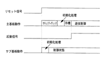
図33に例示するように、この実施の形態で用いられる主基板31のCPU56は、リセット信号がリセット解除状態を示すと、まず、セキュリティチェックプログラムを実行し、その後初期化処理を実行する。また、サブ基板35,37,70,80のCPUは、リセット信号がリセット解除状態を示すと、初期化処理を実行した後に遊技演出に関わる制御を行う状態である制御状態に入る。そして、立上管理回路975は、CPU56のセキュリティチェックプログラムの実行が確実に完了するタイミングで起動信号を出力する。起動信号は、主基板31の入出力ポート57に入力される。
【0222】
主基板31のCPU56は、入出力ポート57を介して起動信号を受けたことを確認したら遊技制御状態に入る。従って、遊技制御手段が遊技制御状態に入ったときには、サブ基板35,37,70,80のCPUは既に制御状態になっている。よって、例えば、主基板31から送出された制御コマンドは、サブ基板35,37,70,80のCPUにおいて確実に受信される。
【0223】
図34は、立上管理手段のさらに他の実施の形態を示すブロック図である。図34に示す構成では、主基板31に対するリセット信号の立ち上げタイミングを調整する立上管理回路976が電源基板910に搭載されている。主基板31とサブ基板(ランプ制御基板35、払出制御基板37、表示制御基板70および音声制御基板80)には、電源基板910から、遅延されることなく各種電圧およびリセット信号が供給される。
【0224】
図35に示すように、サブ基板35,37,70,80のCPUは、リセット信号がリセット解除状態を示すと、初期化処理を実行した後に、動作可能信号を出力する。立上管理回路976は、動作可能信号を受信すると、主基板31に対するリセット信号を立ち上げる。リセット信号が立ち上がったことに応じて、主基板31CPU56は、初期化処理を行った後に遊技制御状態に入る。従って、遊技制御手段が遊技制御状態に入ったときには、サブ基板35,37,70,80のCPUは既に制御状態になっている。よって、例えば、主基板31から送出された制御コマンドは、サブ基板35,37,70,80のCPUにおいて確実に受信される。
【0225】
なお、図34に示す構成において、立上管理回路976は、動作可能信号を受信すると、主基板31に対して起動信号を出力するようにしてもよい。そのように構成されている場合には、主基板31に対するリセット信号は、サブ基板35,37,70,80に対するリセット信号と同様のタイミングでリセット解除状態になる。そして、主基板31では、電源基板910からの起動信号が入出力ポート57に入力され、CPU56は、起動信号を受信したら遊技制御状態に入る。
【0226】
また、上記の各実施の形態では、立下管理手段は、各電気部品制御手段への電源断信号の遅延量を調整することによって立ち下げの順序管理を行ったが、他の方法によっても各電気部品制御手段の立ち下げ管理を行うことができる。
【0227】
図36は、立下管理手段の他の実施の形態を示すブロック図である。図36に示す構成では、立下管理手段は、サブ基板35,37,70,80に対するリセット信号を遅延する遅延回路960で実現される。なお、立上管理回路968は、サブ基板35,37,70,80からの動作可能信号に応じて、主基板31に対して起動信号を出力する。また、この実施の形態では、主基板31およびサブ基板35,37,70,80のCPUは、リセット信号がローレベルになったことによって制御動作を停止する。
【0228】
図37に示すように、主基板31に対するリセット信号は、サブ基板35,37,70,80に対するリセット信号よりも早く立ち上がる。しかし、主基板31のCPU56は、起動信号を受けたことに応じて初めて遊技状態に入る。起動信号は、サブ基板35,37,70,80の各CPUが制御状態に入って動作可能信号を出力すると動作可能状態を示すので、主基板31のCPU56が遊技制御状態に入ったとき、すなわち立ち上がったときには、サブ基板35,37,70,80の各CPUは既に制御状態に入っている。すなわち、既に立ち上がっている。
【0229】
そして、遊技機への電源供給が断してVSLが所定値以下になると、リセットIC651の出力がローレベルになる。リセットIC651の出力は、そのまま主基板31に供給されているが、サブ基板35,37,70,80には遅延回路960を介して供給されている。従って、図37に示すように、主基板31のCPU56は、サブ基板35,37,70,80の各CPUよりも早く立ち下がる。
【0230】
よって、例えば、電源断直前に遊技制御手段が他の電気部品制御手段に対して制御コマンドを送出しているような場合でも、その制御コマンドは、受信側の電気部品制御手段において確実に受信される。
【0231】
なお、図36に示す構成では、1つの遅延回路960の出力が各サブ基板35,37,70,80に供給されているので、各サブ基板35,37,70,80のCPUは同時に立ち下がることになるが、バッファ回路961〜964の前段にそれぞれ遅延回路を置き、各遅延回路の遅延量に差を設ければ、主基板31および各サブ基板35,37,70,80の立ち下げ順序を任意に設定することができる。
【0232】
また、図36に示す構成では、リセットIC651の出力がそのまま遅延回路960およびバッファ回路965に出力されるので、電源投入時に1回のリセット解除動作(ローレベルからハイレベルへの変化)が行われることになるが、図12に示されたようなIC941〜949を設け、2回のリセット解除動作が行われるように構成してもよい。
【0233】
図38は、立下管理手段の他の実施の形態を示すブロック図である。図38に示す構成では、立下管理回路977は、電源監視用IC902の出力がハイレベルからローレベルに変化すると、スイッチ回路978を介して、主基板31に供給される各種電圧を直ちに遮断する。各サブ基板35,37,70,80に至る各種電源については特に制御を行わない。よって、各サブ基板35,37,70,80に供給される電圧はしばらくの間、各サブ基板35,37,70,80が動作可能な電位を維持するが、主基板31に供給される電圧は直ちに遮断される。その結果、主基板31は、各サブ基板35,37,70,80よりも早く立ち下がることになる。
【0234】
図39は、立上管理手段の他の実施の形態を示すブロック図である。図38に示す構成では、立上管理手段であるリセット管理回路940において、リセットIC931,932が設けられている。リセットIC931,932として、図11等に示された電源監視用ICと同じICを用いることができる。リセットIC931は、+30V電源電圧(VSL)が+9V以上になると出力をハイレベルにし、+9Vを下回ると出力をローレベルにする。リセットIC931の出力は、各サブ基板に搭載されたCPUに対してシステムリセット信号として供給される。
【0235】
リセットIC932は、+30V電源電圧(VSL)が+7V以上になると出力をハイレベルにし、+7Vを下回ると出力をローレベルにする。リセットIC931の出力は、主基板31に搭載されたCPU56に対してシステムリセット信号として供給される。リセットIC931,932において、それぞれのVs 端子に、+30V電源電圧が抵抗で分圧された電圧が入力されている。そして、リセットIC931,932が、+30V電源電圧(VSL)と+7Vまたは+9Vとを比較できるように各抵抗の抵抗値が選定されている。
【0236】
図39に示すように、異なる電圧を監視してリセット信号を出力する2つのリセットIC931,932を設けた構成によっても、主基板31のCPU56に対するリセット解除のタイミングを、サブ基板のCPUに対するリセット解除のタイミングよりも遅くすることができる。
【0237】
なお、リセットIC931,932の出力がハイレベルに立ち上げるときには、立ち上がりタイミングが、コンデンサC1,C2の容量で定まる時間だけ遅延される。
【0238】
従って、図40に示すように、遊技機に電源投入がなされ、VSLが+7Vにまで立ち上がると、その時点からコンデンサC1の容量で定まる時間だけ遅延してリセットIC931の出力がハイレベルに立ち上がる。また、VSLが+9Vにまで立ち上がると、その時点からコンデンサC2の容量で定まる時間だけ遅延してリセットIC932の出力がハイレベルに立ち上がる。各サブ基板におけるCPUは、リセットIC931の出力がハイレベルに立ち上がるとリセット解除されて動作を開始するのであるが、各CPUの初期化処理時間の相違等に起因して、本来の制御を開始するタイミングがばらつくことがある。
【0239】
そこで、この実施の形態では、コンデンサC2の容量をコンデンサC1の容量よりも大きくして、リセットIC932の出力がハイレベルに立ち上がるタイミングをより遅くする。そのように構成すれば、各サブ基板におけるCPUの制御開始タイミングがばらついても、主基板31のCPU56が動作開始したときに全てのサブ基板におけるCPUが必ず制御を開始しているようにすることができる。また、電源断時には、主基板31へのリセット信号は+9Vレベルで立ち下がり、VSLの+7Vまでの低下を検出した時点で各サブ基板が立ち下がるので、主基板31を先に立ち下げることができる。
【0240】
なお、図39に示された構成では、電源投入時に1回だけリセット信号が立ち上がるが、図12に示されたように、電源投入時にリセット信号において2回の立ち上がりが発生するように構成してもよい。
【0241】
上記の各実施の形態では、複数の電気部品制御基板を備えた構成において、立上管理手段が各電気部品制御基板の立ち上げ順序を制御することが可能になっている。従って、払出制御基板37を主基板31よりも早く立ち上げたり、表示制御基板70,ランプ制御基板35および音声制御基板80等の遊技演出に関わる制御手段を搭載した電気部品制御基板(演出制御用基板)を主基板31よりも早く立ち上げるように制御することが容易である。
【0242】
また、立下管理手段が各電気部品制御基板の立ち下げ順序を制御することが可能になっている。よって、払出制御基板37を主基板31よりも遅く立ち下げたり、表示制御基板70、ランプ制御基板35および音声制御基板80等の遊技演出に関わる制御手段を搭載した演出制御用基板を主基板31よりも遅く立ち下げるように制御することが容易である。
【0243】
ところで、主基板31におけるCPU56および払出制御基板37における払出制御用CPU371は、電力供給停止時に、電源基板910からの電源断信号に応じて電力供給停止準備処理を行い、その後、ループする動作を行う(図20および図26参照)。電力供給停止時には、さらにその後にシステムリセット信号がローレベルになってCPUはリセット状態になる。
【0244】
しかし、極めて短い電源の瞬断が発生した場合には、システムリセット信号がローレベルにならない可能性がある。上記の各実施の形態では、電源断信号は+30V電源電圧が+22Vを下回ると発生し、システムリセット信号は+30V電源電圧が+9Vを下回るとシステムリセット信号がローレベルになるので、+30V電源電圧が+22Vよりも低下するが+9Vにまで低下しないうちに復旧するような電源瞬断が発生した場合には、電源断信号が発生するので電力供給停止準備処理が実行開始されるが、システムリセット信号はローレベルにならない。そのような場合には、CPUは、電力供給停止準備処理におけるループ処理から抜けることができない。
【0245】
図41は、極めて短い電源の瞬断が発生した場合でも電力供給停止準備処理におけるループ処理から抜け出せないような事態を回避しうる電源基板の一構成例を示すブロック図である。図41に示す構成では、電源監視用IC903が搭載されている。電源監視用IC903は、+30V電源電圧(VSL)が20Vを下回ると出力(RESET端子の出力)をローレベルにする。なお、図41では、電源監視用IC902,903において、それぞれのVs 端子に、+30V電源電圧が抵抗で分圧された電圧が入力されている。そして、電源監視用IC902,903が、+30V電源電圧(VSL)と+22Vまたは+20Vとを比較できるように各抵抗の抵抗値が選定されている。また、IC918の出力は、電源断信号として主基板31および払出制御基板37に供給される。
【0246】
電源監視用IC902の出力はラッチ回路981でラッチされ、ラッチ回路981の出力は、双方の入力がともにローレベルになるとローレベルを出力する論理回路(等価的にOR回路であるから、以下、OR回路と呼ぶ。)982の一方の入力端子に入力される。また、電源監視用IC903の出力は、いずれかの入力がローレベルになるとローレベルを出力する論理回路(等価的にAND回路であるから、以下、AND回路と呼ぶ。)の他方の入力端子に入力される。そして、OR回路982の出力とリセット管理回路940の出力とがAND回路983に入力され、AND回路983の出力はリセット信号として各基板に供給される。
【0247】
なお、図41には、説明を簡単にするために、主基板31および払出制御基板37に同一の電源断信号が供給される構成が示されているが、既に説明したように、主基板31と払出制御基板37とのそれぞれに対応した電源断信号を作成し、払出制御基板37への電源断信号を遅延させてもよい。また、リセット管理回路940は既に説明した実施の形態の場合と同様に、各基板へのリセット信号をそれぞれ作成し、主基板31へのリセット信号を遅延させてもよい。
【0248】
図42(A)は、電源監視用IC903等が設けられていない場合の電源断信号とシステムリセット信号との関係の一例を示す説明図である。図42(A)に示された例では、+30V電源電圧(VSL)は、+22Vを下回ったものの、+9Vにまで低下する前に復旧している。従って、電源断信号(ローアクティブ)は出力されるが、リセット信号はハイレベルのままである。このような場合には、CPUは、電力供給停止準備処理におけるループ処理から抜け出せない。
【0249】
しかし、図41に示された構成によれば、図42(B)に示すように、+30V電源電圧(VSL)が+22Vを下回ると、ラッチ回路981においてローレベルがラッチされ、+30V電源電圧(VSL)が+20Vを下回ると電源監視用IC903の出力がローレベルになるので、OR回路982の出力がローレベルになる。その結果、AND回路983の出力がローレベルになる。すなわち、システムリセット信号がローレベルになる。よって、CPUがシステムリセットされ、ループ処理から抜け出すことができる。
【0250】
電源断信号がローレベルに変化すると電力供給停止準備処理が実行されるが、電力供給停止準備処理が完了した後、リセット信号がリセット解除を示すハイレベルに戻るので、CPUは、停電復旧時の処理と同様の処理を行った後に、通常の制御処理状態に戻る。すなわち、遊技機は、電力供給停止準備処理を実行するがすぐに停電復旧処理を行うので、遊技状態は電源瞬断の前後で食い違うことはない。すなわち、遊技者から見ると電源瞬断など生じなかったように遊技が継続されていることになる。
【0251】
なお、電源断信号がローレベルになるタイミングと電源監視用IC903の出力がローレベルになるタイミングとの間で電力供給停止準備処理が完了している必要があるが、その間の時間が短いような場合には、電源監視用IC903の出力を遅延させる遅延回路を設ければよい。
【0252】
図43は、電源基板910の他の構成例を示すブロック図である。図43に示す構成では、電源監視用IC902の出力が遅延回路984を介してAND回路983の一方の入力端子に入力される。また、AND回路983の他方の入力端子には、リセット管理回路940の出力が入力される。
【0253】
図43に示された構成によれば、図44に示すように、+30V電源電圧(VSL)が+22Vを下回ると、電源監視用IC902の出力(電源断信号)がローレベルになる。その信号は、遅延回路986で遅延されてAND回路983に入力されるので、主基板31や払出制御基板37に供給されるシステムリセット信号がローレベルになる。よって、CPUがシステムリセットされ、ループ処理から抜け出すことができる。なお、遅延回路984における遅延量は、主基板31のCPU56や払出制御基板37の払出制御用CPU371が電力供給停止準備処理を完了するのに十分な時間に設定される。
【0254】
電源断信号がローレベルに変化すると電力供給停止準備処理が実行されるが、電力供給停止準備処理が完了した後、リセット信号がリセット解除を示すハイレベルに戻るので、CPUは、停電復旧時の処理と同様の処理を行った後に、通常の制御処理状態に戻る。すなわち、遊技機は、電力供給停止準備処理を実行するがすぐに停電復旧処理を行うので、遊技状態は電源瞬断の前後で食い違うことはない。すなわち、遊技者から見ると電源瞬断など生じなかったように遊技が継続されていることになる。
【0255】
なお、図43には、説明を簡単にするために、主基板31および払出制御基板37に同一の電源断信号が供給される構成が示されているが、既に説明したように、主基板31と払出制御基板37とのそれぞれに対応した電源断信号を作成し、払出制御基板37への電源断信号を遅延させてもよい。また、リセット管理回路940は既に説明した実施の形態の場合と同様に、各基板へのリセット信号をそれぞれ作成し、主基板31へのリセット信号を遅延させてもよい。
【0256】
図45は、極めて短い電源の瞬断が発生した場合等であってもシステムリセット信号をローレベルにすることができ、その結果、ループ処理を含む電力供給停止準備処理におけるループ処理から抜け出せることができる構成の他の例を示すブロック図である。図45には、電源基板910に搭載された各回路のうちの一部が示されている。電源基板910における各電圧作成部分は例えば図11に示されたような構成でよい。
【0257】
図45に示された構成では、リセット信号を発生するリセットIC932に供給されるVSLと接地レベルとをスイッチングするスイッチ回路933が設けられている。スイッチ回路933は例えばアナログスイッチ回路で構成され、電源監視用IC902の出力(電源断信号)が遅延回路984で遅延された信号を制御信号として、制御信号のレベルに応じてスイッチングされる。リセットIC932は、+30V電源電圧(VSL)を監視して、そのレベルが+9Vを越えると出力をハイレベルにし、+9Vを下回ると出力をローレベルにする。
【0258】
図46は、図45に示された各回路の出力と電源電圧の変化の例を示すタイミング図である。この例では、スイッチ回路933は、制御信号がローレベルであると接地レベルを選択し、ハイレベルであるとVSLを選択する。
【0259】
遊技機の電源が投入されると、図46に示すように、VSLの値が徐々に上昇し、その値が+22Vを越えると電源監視用IC902の出力がハイレベルになる。そのハイレベルは、遅延回路984で所定時間遅延されてスイッチ回路933に伝達される。遅延回路984の出力がハイレベルになると、リセットIC932にVSLが供給される。この値は+9Vを越えているので、リセットIC932の出力すなわち電気部品制御基板に供給されるシステムリセット信号がハイレベルになる。
【0260】
図46に示すように、+30V電源電圧(VSL)が+22Vを下回ると、電源監視用IC902の出力(電源断信号)がローレベルになる。その信号は、電源断信号として、主基板31や払出制御基板37に出力される。従って、主基板31や払出制御基板37において、電力供給停止準備処理が開始される。電源監視用IC902のローレベルの出力は遅延されてローレベルの制御信号としてスイッチ回路933に与えられる。遅延回路933の出力がローレベルになると、リセットIC932に供給される電圧は0Vになる。この値は+9Vを下回っているので、リセットIC932の出力はローレベルになる。すなわち、リセット信号がリセットレベルになる。
【0261】
極めて短い時間の電源瞬断では、図46に例示するようにVSLのレベルが復旧する。従って、電源監視用IC902の出力はハイレベルに戻る。ハイレベルの信号は遅延回路984で遅延されてスイッチ回路933に出力される。よって、リセットIC932に供給される電圧はVSLに戻る。この値は+9Vを越えているので、リセットIC932の出力はハイレベルに戻る。すなわち、システムリセット信号がリセット解除レベルになる。
【0262】
従って、図45に示された構成によっても、極めて短い時間の電源瞬断が生じたような場合でも、主基板31や払出制御基板37に供給されるシステムリセット信号がローレベルになる。よって、CPUがシステムリセットされ、電力供給停止準備処理のループ処理から抜け出すことができる。なお、遅延回路984の遅延量は、電力供給停止準備処理が確実に実行完了する程度の時間に設定される。
【0263】
電力供給停止準備処理が完了した後、リセット信号がリセット解除を示すハイレベルに戻るので、CPUは、停電復旧時の処理と同様の処理を行った後に、通常の制御処理状態に戻る。すなわち、遊技機は、電力供給停止準備処理を実行するがすぐに停電復旧処理を行うので、遊技状態は電源瞬断の前後で食い違うことはない。すなわち、遊技者から見ると電源瞬断が生じてもすぐに遊技の継続が可能になる。
【0264】
なお、図45に示された実施の形態では、遊技機に対する電源投入時に、システムリセット信号がハイレベルになるタイミングが遅れることになるが、遊技開始に支障を来すほどの長さではない。
【0265】
また、図45に示された例では、説明を簡単にするために、主基板31および払出制御基板37に同一の電源断信号が供給される構成が示されているが、既に説明したように、主基板31と払出制御基板37とのそれぞれに対応した電源断信号を作成し、払出制御基板37への電源断信号を遅延させてもよい。また、既に説明した実施の形態の場合と同様に、主基板31へのリセット信号を遅延させてもよい。
【0266】
以上のように、図41、図43および図45に例示された構成によれば、停電等の発生時に遊技状態を保存するように構成された遊技機において、極めて短い時間の電源瞬断が生じたような場合でも、電力供給停止準備処理のループ処理から抜け出すことができないという不都合は生じない。従って、遊技機の制御が停止してしまったりするような問題が生ずることはなく、停電等の発生時に遊技状態を保存するための構成が遊技制御状態に矛盾を生じさせるようなことが防止される。
【0267】
また、図41、図43および図45に示された構成はそれぞれ一例であって、電力供給停止準備処理の最後の部分でループ処理するように構成されている場合において極めて短い時間の電源瞬断等が生じたときに、電力供給停止準備処理を実行するCPUに対するシステムリセット信号をリセットを示すレベルにすることができれば、他の構成を採用することもできる。また、図41、図43および図45に示された構成では、説明を簡単にするために、システムリセット信号がローレベルになった後1回のリセット解除動作(ハイレベルへの変化)が行われる場合を示したが、図12に示されたようなIC941〜949を設け、2回のリセット解除動作が行われるように構成してもよい。
【0268】
さらに、図41、図43および図45に示された各例ではシステムリセット信号を生成するための回路が電源基板910に搭載されていたが、システムリセット信号を生成するための回路が各電気部品制御基板に搭載されている場合であっても、電力供給停止準備処理を実行するCPUに対するリセット信号をリセットを示すレベルにすることができる。
【0269】
なお、上述した説明から明らかなように、制御手段に対して作動の許容と作動の停止とを示すリセット信号を供給するリセット信号作成手段は、立上管理手段と兼用することが可能である。また、遊技機に供給される電源の状態を監視する電源監視手段は、立下管理手段の一部として兼用することが可能である。すなわち、立下管理手段は、制御手段に対して作動の停止を示すリセット信号を供給するリセット信号作成手段と電源断信号を発生する電源監視手段とを含む構成とすることができる。
【0270】
【発明の効果】
以上のように、本発明によれば、遊技機を、遊技機に設けられている電気部品を制御するためのマイクロコンピュータを含む制御手段と、電気部品の制御に関わり変動する制御データを遊技機への電力供給停止時にも保持可能な変動データ記憶手段と、遊技球が入賞領域に入賞したことを検出し、賞球を払い出すためにマイクロコンピュータに検出出力する遊技球検出スイッチと、交流電源からの交流を直流に変換する整流手段と、整流手段によって変換された直流電圧から該直流電圧よりも低い電圧であって遊技機で用いられる遊技球検出スイッチに供給される直流電圧および該遊技球検出スイッチに供給される直流電圧よりもさらに低い電圧であってマイクロコンピュータの駆動電源である直流電圧を生成する直流電圧生成手段と、遊技球検出スイッチに供給される直流電圧よりも高い電圧であって整流手段によって交流から直流に変換された直後の直流電圧を監視し、該監視している直流電圧が遊技球検出スイッチに供給される直流電圧よりも高い第1の電圧に低下したことを検出したときに検出信号を出力する第1の電源監視手段と、マイクロコンピュータに対して作動の許容と作動の停止とのいずれかを示すリセット信号を供給するリセット信号作成手段とを備え、マイクロコンピュータは、第1の電源監視手段からの検出信号の入力に応じて変動データ記憶手段の記憶内容が正常であるか否かを診断するためのチェックデータを生成して当該変動データ記憶手段に保存する処理を含む電力供給停止準備処理を実行し、リセット信号作成手段は、遊技機で使用される電源電圧を監視し、電源電圧が第1の電圧よりも低い第2の電圧となったことを検出する第2の電源監視手段と、電源電圧が第2の電圧よりも低い第3の電圧となったことを検出する第3の電源監視手段とを含み、第2の電源監視手段により電源電圧が第2の電圧を下回ったことを検出したときにリセット信号の状態をマイクロコンピュータの作動の停止を示す状態にし、マイクロコンピュータの作動の停止を示す状態にした後、電源電圧が第3の電圧にまで低下したことを第3の電源監視手段により検出することなく、第2の電源監視手段により第2の電圧に回復したことを検出したときは、さらにリセット信号の状態をマイクロコンピュータの作動の許容を示す状態とし、監視する直流電圧が、第1の電源監視手段が検出信号を出力したあとリセット信号作成手段がリセット信号の状態をマイクロコンピュータの作動の停止を示す状態とするまでの所定期間内にマイクロコンピュータにより電力供給停止準備処理が完了するように設定された第2の電圧を下回ったときに、リセット信号の状態をマイクロコンピュータの作動の停止を示す状態にするように構成したので、停電等の発生時に遊技状態を保存するように構成された遊技機において、ごく短時間の電源瞬断等が生じても所定のリセット信号が制御手段に与えられるので、制御状態に支障を来すことを防止できる効果がある。また、電源の監視によって、容易に、ごく短時間の電源瞬断等が生じても制御状態に支障を来さないようにすることができる。また、リセット信号作成手段は、電力供給停止準備処理が完了した後にマイクロコンピュータをシステムリセットすることができる。さらに、電源復旧時等にチェックデータにもとづいてデータが破壊されていないかどうかチェックするように構成することが可能になり、保存されるデータの信頼性を向上させることができる。
【0275】
リセット信号作成手段が、リセット信号を、断続的に2回、作動の許容を示す状態にする場合には、遊技機の電源投入時やごく短時間の電源瞬断発生時に確実にマイクロコンピュータが起動または再起動し、遊技開始や遊技継続に不都合を生じさせることがないという効果がある。
【0277】
遊技制御用マイクロコンピュータが電力供給停止準備処理を実行するように構成されている場合には、停電等が生じても、電源復旧時に確実に遊技状態を復元できるように必要なデータを保存することができる。
【0278】
払出制御用マイクロコンピュータが電力供給停止準備処理を実行するように構成されている場合には、停電等が生じても、遊技者に対して未払出の価値に関するデータを保存する処理を行うことができ、電源復旧時に保存されていたデータにもとづく価値付与を続行できるので、遊技者に不利益が与えられることが防止される。
【0279】
リセット信号作成手段が、電気部品制御基板を作動状態にした後に遊技制御基板を作動状態にするように構成されている場合には、遊技制御用マイクロコンピュータが他のマイクロコンピュータに対して制御コマンドを送出したときにマイクロコンピュータが立ち上がっていないということはなく、制御コマンドは確実に受信される。
【図面の簡単な説明】
【図1】パチンコ遊技機を正面からみた正面図である。
【図2】パチンコ遊技機の裏面に配置されている各基板を示す背面図である。
【図3】パチンコ遊技機の機構板を背面からみた背面図である。
【図4】遊技制御基板(主基板)の回路構成を示すブロック図である。
【図5】払出制御基板の回路構成例を示すブロック図である。
【図6】表示制御基板の回路構成例を示すブロック図である。
【図7】ランプ制御基板の回路構成例を示すブロック図である。
【図8】音声制御基板の回路構成例を示すブロック図である。
【図9】発射制御基板の回路構成例を示すブロック図である。
【図10】電源基板から各基板に供給される直流電圧等を示すブロック図である。
【図11】電源基板の一構成例を示すブロック図である。
【図12】リセット管理回路の構成例を示すブロック図である。
【図13】リセットICとその周辺のICの出力信号の様子を示すタイミング図である。
【図14】主基板におけるCPUが実行するメイン処理の例を示すフローチャートである。
【図15】遊技状態復旧処理を実行するか否かの決定方法の例を示す説明図である。
【図16】初期設定処理の例を示すフローチャートである。
【図17】初期化処理の例を示すフローチャートである。
【図18】2msタイマ割込処理の例を示すフローチャートである。
【図19】遊技制御処理の例を示すフローチャートである。
【図20】停電発生NMI処理の例を示すフローチャートである。
【図21】バックアップパリティデータ作成方法の例を説明するための説明図である。
【図22】払出制御用CPUが実行するメイン処理の例を示すフローチャートである。
【図23】払出制御用CPUの初期化処理の一例を示すフローチャートである。
【図24】払出制御用CPUのタイマ割込処理の例を示すフローチャートである。
【図25】払出制御用CPUが実行する払出制御処理の例を示すフローチャートである。
【図26】停電発生NMI処理の例を示すフローチャートである。
【図27】バックアップパリティデータ作成方法の例を説明するための説明図である。
【図28】払出制御用CPUが実行する払出状態復旧処理の例を示すフローチャートである。
【図29】遊技機の電源断時の電源低下やNMI信号の様子の例を示すタイミング図である。
【図30】電源基板の他の構成例を示すブロック図である。
【図31】各基板に供給される直流電圧等を示すブロック図である。
【図32】立上管理手段のさらに他の実施の形態を示すブロック図である。
【図33】図32に示す立上管理手段の動作を説明するためのタイミング図である。
【図34】立上管理手段のさらに他の実施の形態を示すブロック図である。
【図35】図34に示す立上管理手段の動作を説明するためのタイミング図である。
【図36】立下管理手段の他の実施の形態を示すブロック図である。
【図37】図35に示す立下管理手段の動作を説明するためのタイミング図である。
【図38】立下管理手段のさらに他の実施の形態を示すブロック図である。
【図39】立上管理手段の他の実施の形態を示すブロック図である。
【図40】図39に示す立上管理手段の動作を示すタイミング図である。
【図41】電源基板の他の構成例を示すブロック図である。
【図42】電源断信号とリセット信号の関係を示す説明図である。
【図43】電源基板のさらに他の構成例を示すブロック図である。
【図44】電源断信号とリセット信号の関係を示す説明図である。
【図45】電源基板の一部を示すブロック図である。
【図46】図45に示された各回路の出力と電源電圧の変化の例を示すタイミング図である。
【符号の説明】
1 パチンコ遊技機
31 主基板
35 ランプ制御基板
37 払出制御基板
56 CPU
70 表示制御基板
80 音声制御基板
371 払出制御用CPU
910 電源基板
902 電源監視用IC
920 遅延回路
932 リセットIC
940 リセット管理回路
960 遅延回路
971,972,973,974 遅延回路
968,975,976 立上管理回路
977 立下管理回路[0001]
TECHNICAL FIELD OF THE INVENTION
The present invention relates to a gaming machine such as a pachinko gaming machine, a coin gaming machine, a slot machine, and the like in which a game is performed according to a player's operation, and in particular, a game is performed according to a player's operation in a gaming area of a gaming board. Related to gaming machines.
[0002]
[Prior art]
As an example of a gaming machine, when a game medium such as a game ball is fired into a game area by a launching device and a game medium wins a winning area such as a winning opening provided in the game area, a predetermined number of prize balls are played by a player. Some are paid out. Further, a variable display unit whose display state can be changed is provided, and when a display result of the variable display unit becomes a predetermined specific display mode, a predetermined game value is provided to the player. There is.
[0003]
In addition, the game value is a right to make the state of the variable prize ball device provided in the game area of the gaming machine advantageous for a player who is easy to win a hit ball, or to a state advantageous to the player. Or that the condition for prize game medium payout becomes easy to be satisfied.
[0004]
In a pachinko gaming machine, when a display result of a variable display unit that displays a special symbol is a combination of a predetermined specific display mode, it is generally referred to as a “big hit”. When a big hit occurs, for example, the big winning opening is opened a predetermined number of times, and the state shifts to a big hit game state in which a hit ball is easy to win. Then, in each open period, when a predetermined number (for example, 10) of the winning prizes is won, the winning prize opening is closed. The number of opening of the special winning opening is fixed to a predetermined number (for example, 16 rounds). An opening time (for example, 29.5 seconds) is determined for each opening, and if the opening time elapses even if the number of winnings does not reach a predetermined number, the winning opening is closed. If the predetermined condition (for example, winning in the V zone provided in the special winning opening) is not satisfied at the time when the special winning opening is closed, the big hit gaming state ends.
[0005]
Also, among the combinations of display modes other than the combination of “big hits”, at the stage where some of the display results of the plurality of variable display units have not yet been derived and displayed, the variable display in which the display results have already been derived and displayed. A state in which the display mode of the unit satisfies the display condition that is a combination of the specific display modes is called “reach”. If the display result of the identification information variably displayed on the variable display unit does not satisfy the condition of “reach”, the result is “out” and the variable display state ends. A player plays a game while enjoying how to generate a big hit.
[0006]
The game progress in the gaming machine is controlled by game control means such as a microcomputer. The identification information, the character image, and the background image displayed on the variable display device are controlled by a display control unit that operates according to display control command data from the game control unit. Generally, the identification information, the character image, and the background image displayed on the variable display device include a microcomputer for display control and a video display processor that generates image data in accordance with instructions from the microcomputer and transfers the image data to the variable display device ( VDP), and the display control microcomputer has a large program capacity.
[0007]
Therefore, the microcomputer of the game control means having a limited program capacity cannot control the identification information and the like displayed on the variable display device, and the display control microcomputer (microcomputer) is different from the microcomputer of the game control means. Display control means). Therefore, the game control means for controlling the progress of the game needs to transmit a command for display control to the display control means.
[0008]
When a game ball wins a winning opening provided on the game board, a predetermined number of award balls are paid out. Since the progress of the game is controlled by the game control means mounted on the main board, the number of winning balls based on the winning is determined by the game control means and transmitted to the payout control board controlling the payout device.
[0009]
Further, in such a gaming machine, a speaker is provided, and various effect sounds are emitted from the speaker as the game progresses in order to enhance a gaming effect. In addition, a light-emitting body such as a lamp or an LED is provided in a game area or a frame of the gaming machine, and the light-emitting body is turned on or off as the game progresses in order to enhance the game effect. Since the sound from the speaker and the lighting / extinguishing of each light emitter are controlled in accordance with the progress of the game, these controls are generally performed by game control means for controlling the progress of the game. In this case, if a voice control unit provided separately from the game control unit and specifically controls the speaker and a luminous body control unit performing specific control on the luminous body are provided, the control load of the game control unit is reduced. be able to.
[0010]
As described above, the gaming machine may be equipped with various control means in addition to the game control means. In that case, the game control means for controlling the progress of the game transmits each command indicating an operation instruction to each control means mounted on each control board according to the game situation. Hereinafter, each control means mounted on the game control board and other control boards may be referred to as an electric component control means. Hereinafter, the game control board and other control boards may be referred to as electric component control boards. The payout control unit is an example of a value assignment control unit.
[0011]
The electric component control means in each electric component control board is often realized by a microcomputer. When a microcomputer is used, it is necessary to provide a reset state to the microcomputer when the power is turned on, and thereafter to release the reset state. Therefore, each electric component control board is provided with a circuit for generating a reset signal.
[0012]
Further, when a power failure or the like occurs in the gaming machine and the power is restored, the gaming state immediately before the power failure or the like occurs is canceled and the game is restarted from the initial state. In this case, if the game state immediately before the occurrence of the power failure or the like is an advantageous game state for the player, disadvantages may be given to the player due to the power failure or the like. In order to prevent such inconvenience, it is only necessary to detect the occurrence of a power failure or the like and save the game state before the power is completely turned off. Then, when the power is restored, the saved game state may be restored. The occurrence of a power failure or the like is generally detected by detecting that the power supply voltage level has fallen below a predetermined value.
[0013]
[Problems to be solved by the invention]
However, even if it is detected that the level of the power supply voltage has dropped below a predetermined value, there is a possibility that the power supply is restored without being turned off. For example, when an instantaneous power interruption occurs for a very short period of time, the level of the power supply voltage drops, but the value may not return to 0 or a value close to it and may be restored to a normal level. In this case, even if the occurrence of a power failure or the like is detected and the predetermined game state saving process is started, there is a possibility that the power is not turned off and the operation state of the game machine is inconsistent.
[0014]
Therefore, the present invention provides a gaming machine that is configured to save the gaming state when a power failure or the like occurs, and that does not interfere with the control state even when a short-time power interruption or the like occurs for a very short time. The purpose is to provide.
[0015]
[Means for Solving the Problems]
A gaming machine according to the present invention is a gaming machine in which a player plays a predetermined game and pays out a prize ball to the player in response to a game ball winning in a winning area provided in the game area. Control means including a microcomputer for controlling electric components provided in the machine, and fluctuation data storage means capable of holding control data that fluctuates in relation to control of the electric components even when power supply to the gaming machine is stopped, A game ball detection switch that detects when a game ball has won a prize area and detects and outputs it to a microcomputer in order to pay out a prize ball, a rectifier that converts AC from an AC power supply to DC, and a rectifier. From the applied DC voltage is lower than the DC voltage Voltage DC voltage supplied to the game ball detection switch used in the gaming machine and A voltage lower than the DC voltage supplied to the game ball detection switch; DC voltage generating means for generating a DC voltage that is a drive power supply of the microcomputer, A voltage higher than the DC voltage supplied to the game ball detection switch, The DC voltage immediately after conversion from AC to DC by the rectifier is monitored, Monitoring First power supply monitoring means for outputting a detection signal when detecting that the DC voltage has dropped to a first voltage higher than the DC voltage supplied to the game ball detection switch; And a reset signal generating means for supplying a reset signal indicating either of the stop of the operation and the resetting of the operation of the microcomputer. A power supply stop preparation process including a process of generating check data for diagnosing whether or not the power supply is normal and storing the check data in the variation data storage unit is performed. A second power supply monitoring unit that monitors the voltage and detects that the power supply voltage has become a second voltage lower than the first voltage; and a third power supply monitoring unit that has a power supply voltage lower than the second voltage. And a third power supply monitoring means for detecting that the power supply voltage has become lower than the second power supply monitoring means. After the power supply voltage has dropped to the third voltage, the third power supply monitoring means does not detect that the power supply voltage has dropped to the third voltage. When the recovery of the second voltage is detected by the means, the state of the reset signal is further set to a state indicating permission of operation of the microcomputer, The DC voltage to be monitored is First power supply monitoring means detects Signal output Reset signal creation means But Within a predetermined period until the state of the reset signal changes to a state indicating that the microcomputer has stopped operating, the microcomputer Power supply stop preparation processing is completed Do When the voltage falls below the second voltage set , The state of the reset signal is a state indicating that the operation of the microcomputer is stopped.
[0016]
Microcomputer Are determined at the start of power supply based on the check data to determine whether or not the storage contents of the fluctuation data storage means are normal. When the determination result of the determination means is normal, the fluctuation data storage means Power supply start time processing means for executing a game state restoration process for restarting the control based on the held data and executing an initialization process when the judgment result of the judgment means is not normal. .
[0020]
The reset signal generating means may be configured to be capable of setting the reset signal intermittently twice to a state indicating permission of operation.
[0022]
Microcomputer Game control to control the game progress Microcomputer There is a game control Microcomputer May be configured to execute a power supply stop preparation process.
[0023]
Microcomputer Control to add value to the player Withdrawal control Microcomputer There is Withdrawal control Microcomputer May be configured to execute a power supply stop preparation process. The value is defined as a game medium such as a game ball or a coin which is paid out to a player according to a predetermined condition such as a prize, or a score given to the player according to a predetermined condition such as a prize. That is.
[0024]
A game control board on which game control means for controlling game progress is mounted, and one or more electric component control boards on which control means other than the game control means are mounted; The game control board may be configured to be activated after the activation.
[0025]
BEST MODE FOR CARRYING OUT THE INVENTION
Hereinafter, an embodiment of the present invention will be described with reference to the drawings.
First, the overall configuration of a pachinko gaming machine, which is an example of a gaming machine, will be described. FIG. 1 is a front view of the
[0026]
As shown in FIG. 1, the
[0027]
Near the center of the
[0028]
An opening /
[0029]
The
[0030]
In this example, a
[0031]
The
[0032]
The hit ball fired from the hitting ball launching device enters the
[0033]
The rotation of the image in the
[0034]
If the combination of images in the
[0035]
Next, each board disposed on the back surface of the
As shown in FIG. 2, on the back surface of the
[0036]
On the back side of the gaming machine, a variable
[0037]
Further, a
[0038]
In FIG. 2, signals from the
[0039]
FIG. 3 is a rear view of the mechanical plate of the
[0040]
Although not shown in FIG. 3, a ball distribution member is provided below the
[0041]
On the side of the
[0042]
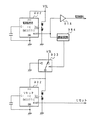
FIG. 4 is a block diagram illustrating an example of a circuit configuration of the
[0043]
Also, according to the data provided from the basic circuit 53, jackpot information indicating occurrence of a jackpot, effective start information indicating the number of start winning balls used for starting image display of the
[0044]
The basic circuit 53 includes a
[0045]
Further, the
[0046]
Further, a reset signal and a power-off signal are supplied from the
[0047]
A hit ball launching device that hits and launches a game ball is driven by a
[0048]
In this embodiment, the lamp control means mounted on the
[0049]
FIG. 5 is a block diagram showing components related to payout, such as components of the
[0050]
The
[0051]
Further, a detection signal from the award
[0052]
When there is a prize, a payout control command indicating the number of prize balls is input to the
[0053]
In this embodiment, the
[0054]
On the
[0055]
The
[0056]
Further, a detection signal from the ball lending count switch 301B is input to the input port 372b of the
[0057]
A ball distribution member is provided below the
[0058]
Further, a reset signal and a power-off signal are supplied from the
[0059]
The
[0060]
A ball lending switch signal and a return switch signal are given from the
[0061]
When the power of the
[0062]
When a predetermined delay time has elapsed from this point, the microcomputer for controlling the card unit outputs a BRQ signal to the
[0063]
As described above, the signal from the
[0064]
Further, the card balance display signal indicating the balance of the prepaid card and the ball lending possible display signal are transmitted to the
[0065]
In this embodiment, the case where the
[0066]
In this embodiment, at least a part or all of the RAM in the
[0067]
In addition, in order to send commands to the
[0068]
FIG. 6 shows a circuit configuration in the
[0069]
A reset signal is supplied from the
[0070]
The display control CPU 101 operates in accordance with a program stored in the
[0071]
Then, the display control CPU 101 controls display of a screen displayed on the LCD 82 according to the received display control command. Specifically, a command corresponding to the display control command is given to the
[0072]
FIG. 6 also shows a
[0073]
The
[0074]
The outputs of the
[0075]
Further, for example, a three-terminal capacitor or a ferrite bead is used as the
[0076]
FIG. 7 is a block diagram showing a signal transmission / reception portion in the
[0077]
A reset signal is supplied from the
[0078]
As shown in FIG. 7, a lamp control command related to lamp control is output from output ports (
[0079]
In the
[0080]
In the
[0081]
Further, the lamp control CPU 351 outputs an on / off signal to the
[0082]
For example, 74HC540 and 74HC14, which are general-purpose CMOS-ICs, are used as the input buffer circuits 355A and 355B. The input buffer circuits 355A and 355B can pass signals only in the direction from the
[0083]
On the
[0084]
FIG. 8 is a block diagram showing a configuration example of a signal transmission portion of a voice control command on the
[0085]
A reset signal is supplied from the
[0086]
As shown in FIG. 8, the voice control command is output from output ports (
[0087]
Then, for example, the voice synthesizing circuit 702 based on the digital signal processor generates a voice or sound effect according to the instruction of the
[0088]
As the
[0089]
On the
[0090]
FIG. 9 is a block diagram showing a
[0091]
The motor drive circuit 813 generates a voltage for controlling the rotation speed of the
[0092]
The
[0093]
FIG. 10 is a block diagram showing a DC voltage and the like supplied from the
[0094]
In this embodiment,
[0095]
As shown in FIG. 10, the ground side of the voltage supplied to each substrate is shared by the
[0096]
FIG. 11 is a block diagram illustrating a configuration example of a
[0097]
Transformer 911 converts an AC voltage from an AC power supply to 24V. The AC 24 V voltage is output to
[0098]
However, the
[0099]
The + 5V line from DC-
[0100]
Note that a battery that can be charged from a + 5V power supply may be used as the backup power supply. In the case of using a battery, a rechargeable battery is used which runs out of capacity when power is not supplied from a + 5V power supply for a predetermined time.
[0101]
A power
[0102]
The predetermined value for the power
[0103]
Further, when VSL (+30 V) is used as the monitoring voltage, since the voltage supplied to various switches of the gaming machine is +12 V, prevention of erroneous switch-on detection at the moment of a power interruption can be expected. That is, if the voltage of the +30 V power supply is monitored, it is possible to detect a decrease in the voltage of +12 V at a stage before +12 V generated after the generation of +30 V starts to fall. Therefore, when the voltage of the + 12V power supply decreases, the switch output comes to the on state. However, if the + 30V power supply voltage that drops earlier than the + 12V is monitored and the power cutoff is recognized, the power supply is turned on before the switch output turns on. It is possible to enter a state of waiting for restoration and to enter a state in which the switch output is not detected.
[0104]
Further, since the power
[0105]
Note that, in the configuration shown in FIG. 11, the detection output (voltage drop signal) of the power
[0106]
Further, a
[0107]
FIG. 12 is a block diagram illustrating a configuration example of the
[0108]
Further, the reset IC 651 monitors the power supply voltage of VSL, which is the power supply voltage equal to the power supply voltage monitored by the power
[0109]
As shown in FIG. 12, the reset signal from the reset IC 651 is input to the
[0110]
The Q6 output of the
[0111]
Then, for example, the detection voltage (voltage at which a voltage drop signal is output) of the power
[0112]
In this example, the first detection condition under which the first power supply monitoring means outputs a detection signal is that the +30 V power supply voltage has dropped to +22 V, and the second power supply monitoring means outputs the detection signal. The second detection condition becomes that the +30 V power supply voltage has dropped to +9 V. However, the voltage value used here is an example, and another value may be used.
[0113]
However, although the monitoring range is narrowed, it is also possible to use a + 5V power supply voltage as the monitoring voltage of the first voltage monitoring circuit and the second voltage monitoring circuit. Also in that case, the detection voltage of the first voltage monitoring circuit is set higher than the detection voltage of the second voltage monitoring circuit.
[0114]
While power is not supplied from the + 5V power supply which is the driving power supply of the
[0115]
FIG. 12 shows a configuration in which a reset signal (low-level signal) is applied twice to the reset terminal of the CPU of each electric component control board when the power is turned on, but the reset signal rises only once. However, in the case of using a CPU whose reset is surely released, the circuit elements indicated by
[0116]
In this embodiment, a reset signal is supplied from the
[0117]
For example, when the
[0118]
FIG. 13 is a timing chart showing output signals of the reset IC 651 of the
[0119]
When the
[0120]
The
[0121]
Therefore, when the power of the gaming machine is turned on, as shown in FIG. 13 as the outputs IC961 to 964 and the output of IC965, the reset terminals of each CPU are once reset (high level) and then reset again (low level). ) Is supplied. That is, when the power is turned on, a low-level signal for resetting each CPU is generated twice. It can also be said that the high level indicating reset release has occurred twice. As a result, each CPU can be reliably started by the second change from the low level to the high level even if it is not started by the change from the low level to the high level indicating the first reset release. Therefore, when the power of the gaming machine is turned on, the game control is reliably started.
[0122]
As shown in FIG. 13, the timing at which the reset signal to the
[0123]
Here, the
[0124]
If each of the electric component control boards is configured to generate a reset signal to be used by itself, it is difficult to adjust the reset release timing of each reset signal. However, in this embodiment, the
[0125]
However, each of the electric component control boards may be configured to generate a reset signal to be used by itself. Then, in each of the electric component control boards, each reset signal generating means is configured such that the reset release timing is a predetermined timing. For example, the respective timings are set so that the reset signal generating means of the
[0126]
In this embodiment, the start-up management unit as illustrated in FIG. 12 is mounted on the
[0127]
Next, the game control operation will be described.
FIG. 14 is a flowchart illustrating a main process executed by the
[0128]
Then, it is checked whether or not the data protection processing of the backup RAM area (for example, the power supply stop preparation processing such as the addition of parity data) has been performed when the power is turned off (step S2). In this embodiment, when an unexpected power interruption occurs, a power supply stop preparation process for protecting data in the backup RAM area is performed. The case where such processing has been performed is referred to as backup. After confirming that there is no backup, the
[0129]
In this embodiment, whether or not there is backup data in the backup RAM area is confirmed by the state of the backup flag set in the backup RAM area when the power is turned off. For example, if "55H" is set in the backup flag area, it means that there is a backup (on state), and if a value other than "55H" is set, it means that there is no backup (off state). “55H” set in the backup flag area is data set when the data protection processing of the backup RAM area is completed in the power supply stop preparation processing, and is a parity code based on the data of the backup RAM area.
[0130]
If there is backup data in the backup RAM area, the
[0131]
If the check result is normal, the
[0132]
When the execution of the normal initialization process (Step S3) is completed, the process shifts to a loop process in which the timer interrupt flag is monitored (Step S9) in the main process. In the loop, a display random number update process (step S8) is also executed.
[0133]
In this embodiment, after the presence or absence of backup data is confirmed in step S2, if backup data exists, the backup area is checked in step S4. Conversely, the backup area check result is After it is confirmed that the data is normal, the presence or absence of backup data may be confirmed. Alternatively, whether to execute the power failure recovery process may be determined by confirming whether there is backup data or checking the backup area.
[0134]
Further, for example, at the time of the parity check (step S4) when determining whether or not to execute the power failure recovery processing, that is, at the time of determining whether or not to restore the gaming state, a special process in the stored RAM data is performed. If it is confirmed that the gaming machine is in a game waiting state (a state in which no symbol is changing, no big hit game is in progress, and there is no start winning prize memory) by a flag or the like or the data of the number of start winning prizes. Alternatively, the initialization process may be performed without performing the game state restoration process.
[0135]
FIG. 16 is a flowchart showing the initial setting process in step S1. In the initial setting process, the
[0136]
The
[0137]
FIG. 17 is a flowchart showing the processing of the normal initialization processing (step S3). As shown in FIG. 17, in the initialization process, a RAM clear process is performed (step S3a). Then, based on the address value of the work area initial setting table, a predetermined work area (for example, a normal symbol determination random number counter, a normal symbol determination buffer, a special symbol left middle right symbol buffer, a payout command storage pointer, etc.) is initialized. An initial value setting process for setting a value (step S3b) is performed.
[0138]
Then, the register of the CTC provided in the
[0139]
Therefore, in this embodiment, the built-in CTC of the
[0140]
When detecting that the timer interrupt flag is set in step S9, the
[0141]
FIG. 19 is a flowchart showing the game control processing in step S11. In the game control process, first, the
[0142]
Next, various abnormality diagnosis processes are performed by the self-diagnosis function provided inside the
[0143]
Next, a process of updating each counter indicating a random number for determination, such as a random number for big hit determination, used for game control is performed (step S23). The
[0144]
Further, the
[0145]
Further, a normal symbol process is performed (step S26). In the normal symbol process process, a corresponding process is selected and executed according to a normal symbol process flag for controlling the
[0146]
Further, the
[0147]
Next, the
[0148]
Further, the
[0149]
Then, the
[0150]
As described above, the main process includes the process of determining whether or not to shift to the game control process, and the internal timer of the
[0151]
Here, the game control process executed by the
[0152]
FIG. 20 is a flowchart illustrating an example of a power failure occurrence NMI process executed in response to an NMI based on a power-off signal from the
[0153]
Next, interrupt prohibition is set (step S42). In the power failure occurrence NMI process, a checksum generation process is performed to ensure that the contents of the RAM are preserved. If other interrupt processing is performed during that processing, the voltage may drop to a level where the CPU cannot operate before the checksum generation processing is completed. Is set so as not to occur. Steps S44 to S50 in the power failure occurrence NMI process are an example of a power supply stop preparation process. If a CPU having a specification that does not cause another interrupt during the interrupt process is used, the process of step S42 is unnecessary.
[0154]
Next, the
[0155]
First, the contents of each register are stored in the backup RAM area (step S44). Thereafter, a backup flag is set (step S45). Then, an appropriate initial value is set in the backup check data area of the backup RAM area (step S46), exclusive OR is sequentially performed on the initial value and the data of the backup RAM area, and the result is inverted (step S47). The calculated value is set in the backup parity data area (step S48). Further, the RAM access is prohibited (step S49). When the power supply voltage decreases, the levels of various signal lines may become unstable and the contents of the RAM may be corrupted. However, if the RAM access is prohibited in this manner, the data in the backup RAM may be corrupted. There is no.
[0156]
Further, the
[0157]
Next, the
[0158]
In this embodiment, in the power failure occurrence NMI process, the program is set in a loop state at the last part, but a HALT instruction may be issued.
[0159]
As described above, the backup flag set after storing the contents of the register in the RAM area determines whether there is backup data to be restored at power-on (whether restoration from a power failure or not). Used when Further, the processing of steps S41 to S50 is completed before the
[0160]
In this embodiment, at the start of the power supply stop preparation process, the backup flag is checked. If the backup flag has already been set, the power supply stop preparation processing is not executed. As described above, the backup flag is a flag indicating that the backup of necessary data has been completed and then the power supply stop preparation processing has been completed. Therefore, for example, even if the NMI occurs again for some reason in the reset-waiting loop state, the power supply stop preparation processing is not executed repeatedly.
[0161]
However, if a CPU having a specification that does not cause another interrupt during the interrupt processing is used, the determination in step S43 is unnecessary.
[0162]
FIG. 21 is an explanatory diagram for describing an example of a backup parity data creation method. However, in the example shown in FIG. 21, the size of the data in the backup data RAM area is 3 bytes for simplicity. In the power failure generation process based on the power supply voltage drop, as shown in FIG. 21, initial data (00H in this example) is set in the backup check data area. Next, an exclusive OR of “00H” and “F0H” is obtained, and an exclusive OR of the result and “16H” is obtained. Further, an exclusive OR of the result and “DFH” is obtained. Then, a value (“C6H” in this example) obtained by inverting the result (“39H” in this example) is set in the backup parity data area.
[0163]
When the power is turned on again, the parity diagnosis is performed in the power failure recovery processing. If all the data in the backup area is stored as it is, the data as shown in FIG. 21 is set in the backup area when the power is turned on again.
[0164]
In the processing of step S4, the
[0165]
Therefore, the
[0166]
As described above, in this embodiment, the game control means is provided with the storage means (backup RAM in this example) which is backed up for a predetermined period of time even when the power of the gaming machine is turned off. The CPU 56 (specifically, a program executed by the CPU 56) is configured to perform a game state restoration process (step S6) for restoring the game state based on the backup data when the storage unit is in the backup state.
[0167]
In this embodiment, in the
[0168]
In the above embodiment, the
[0169]
Further, when an interrupt signal from the power supply board is detected via the IRQ terminal instead of the NMI interrupt signal, an IRQ interrupt mask is set at the start of the game control process in step S11 of the main process, and the game control is performed. The IRQ interrupt mask may be released at the end of the processing. In such a case, an interruption occurs before and after the start of the game control process, so that the game control process is not interrupted halfway. Therefore, there is no possibility that the command transmission is interrupted when the payout control command is transmitted to the
[0170]
FIG. 22 is a flowchart showing the main processing of the
[0171]
Then, the
[0172]
If the backup data exists in the backup RAM area, the
[0173]
If the check result is normal, the
[0174]
After the execution of the normal initialization process (step S703), the main process executed by the
[0175]
In this embodiment, after the presence or absence of backup data is confirmed in step S702, if backup data exists, the backup area is checked in step S704. Conversely, the backup area check result is After it is confirmed that the data is normal, confirmation of the presence or absence of backup data may be performed. Further, it may be configured to determine whether or not to execute the power failure recovery process by confirming whether or not there is backup data or checking the backup area.
[0176]
Also, for example, at the time of a parity check (step S704) when determining whether or not to execute the power failure recovery processing, that is, when determining whether or not to restore the gaming state, the payout in the stored RAM data is performed. If it is confirmed from the game ball number data or the like that the gaming machine is in the payout standby state (not in the middle of payout), the initialization processing may be executed without performing the payout state restoration processing.
[0177]
In the normal initialization process, as shown in FIG. 23, the register and RAM are cleared (step S901), and a predetermined initial value is set (step S902). Then, before the initialization process is completed, an interrupt is permitted (step S903).
[0178]
In this embodiment, the built-in timer / counter of the
[0179]
When detecting that the timer interrupt flag has been set in step S708, the
[0180]
When the power is turned on, the
[0181]
FIG. 25 is a flowchart showing the payout control processing in step S710. In the payout control processing, the
[0182]
Next, the
[0183]
Next, the
[0184]
Also, the
[0185]
In this embodiment, a stepping motor is used as the
[0186]
Next, error detection processing is performed, and a predetermined display is performed on the
[0187]
Further, a process of outputting an information signal to the
[0188]
FIG. 26 is a flowchart illustrating an example of a power failure occurrence NMI process executed in response to an NMI based on a power-off signal from the power
[0189]
In the power failure occurrence NMI process, as in the process executed in the
[0190]
If a CPU having a specification that does not cause another interrupt during the interrupt process is used, the process of step S802 is unnecessary.
[0191]
Next, the
[0192]
First, the contents of each register are stored in the backup RAM area (step S804). Thereafter, a backup flag is set (step S805). Then, an appropriate initial value is set in the backup check data area of the backup RAM area (step S806), exclusive OR is sequentially performed on the initial value and the data of the backup RAM area, and the result is inverted (step S807). The calculated value is set in the backup parity data area (step S808). In addition, the RAM access is prohibited (step S809). When the power supply voltage decreases, the levels of various signal lines may become unstable and the contents of the RAM may be corrupted. However, if the RAM access is prohibited in this manner, the data in the backup RAM may be corrupted. There is no.
[0193]
Further, the
[0194]
Next, the
[0195]
In this embodiment, in the power failure occurrence NMI process, the program is set in a loop state at the last part, but a HALT instruction may be issued.
[0196]
As described above, the backup flag set after storing the contents of the register in the RAM area determines whether there is backup data to be restored at power-on (whether restoration from a power failure or not). Used when Further, the processing of steps S801 to S810 is completed before the
[0197]
In this embodiment, at the start of the power supply stop preparation process, the backup flag is checked. If the backup flag has already been set, the power supply stop preparation processing is not executed. As described above, the backup flag is a flag indicating that the backup of necessary data has been completed and then the power supply stop preparation processing has been completed. Therefore, for example, even if the NMI occurs again for some reason in the reset-waiting loop state, the power supply stop preparation processing is not executed repeatedly.
[0198]
However, when a CPU having a specification that does not cause another interrupt during the interrupt processing is used, the determination in step S803 is unnecessary.
[0199]
Further, in this embodiment, the
[0200]
FIG. 27 is an explanatory diagram for describing an example of a backup parity data creation method. However, in the example shown in FIG. 27, for simplicity, the data size of the backup data RAM area is 3 bytes. In the power failure generation process based on the power supply voltage drop, as shown in FIG. 27, initial data (00H in this example) is set in the backup check data area. Next, an exclusive OR of “00H” and “F0H” is obtained, and an exclusive OR of the result and “16H” is obtained. Further, an exclusive OR of the result and “DFH” is obtained. Then, a value (“C6H” in this example) obtained by inverting the result (“39H” in this example) is set in the backup parity data area.
[0201]
When the power is turned on again, the parity diagnosis is performed in the power failure recovery processing. If all the data in the backup area is stored as it is, the data as shown in FIG. 27 is set in the backup area when the power is turned on again.
[0202]
In the processing of step S704, the
[0203]
Therefore, the
[0204]
Hereinafter, the payout state restoration processing will be described. FIG. 28 is a flowchart showing an example of the payout state restoration processing shown in step S706 of FIG. In this example, the
[0205]
For example, if the number of unpaid prize balls and the number of unpaid lending balls or both of them are stored in the backup RAM area when the power is restored, the payout process is restarted based on the stored numbers.
[0206]
As described above, in this embodiment, the payout control means is provided with the storage means (backup RAM in this example) which is backed up for a predetermined period even if the power of the gaming machine is turned off. The payout control CPU 371 (specifically, a program executed by the payout control CPU 371) performs payout state restoration processing (step S706) for restoring the payout state based on the backup data if the storage unit is in the backup state. Be composed.
[0207]
In the configuration of the
[0208]
Accordingly, as shown in FIG. 29, the NMI is applied to the
[0209]
That is, the fall management means mounted on the
[0210]
Here, the fall management unit controls the sequence of the fall between them by shifting the timing of the power-off signal given to the
[0211]
Then, a delay circuit is placed before each buffer circuit, and if a difference is provided between the delay amounts of the respective delay circuits, a power-off signal output timing given to the
[0212]
Further, as in this embodiment, the fall management means in the
[0213]
In this embodiment, the fall management means is mounted on the
[0214]
In the above-described embodiment, the start-up management unit controls the start-up sequence by adjusting the delay amount of the reset signal to each electric component control unit. It is also possible to control the startup sequence by adjusting.
[0215]
FIG. 30 is a block diagram illustrating a configuration example of a
[0216]
Although one
[0217]
Further, in the
[0218]
Further, not all kinds of voltages used in the electric component control board may be delayed, but only the power supply voltage used by the CPU may be delayed.
[0219]
FIG. 31 is a block diagram showing a DC voltage and the like supplied to each substrate when the
[0220]
FIG. 32 is a block diagram showing still another embodiment of the start-up management means. In the configuration shown in FIG. 32, a start-up
[0221]
As illustrated in FIG. 33, when the reset signal indicates the reset release state, the
[0222]
When the
[0223]
FIG. 34 is a block diagram showing still another embodiment of the start-up management means. In the configuration shown in FIG. 34, a start-up management circuit 976 that adjusts the timing of starting the reset signal for the
[0224]
As shown in FIG. 35, when the reset signal indicates the reset release state, the CPU of the sub-boards 35, 37, 70, and 80 outputs an operation enable signal after executing the initialization processing. Upon receiving the operable signal, the start-up management circuit 976 starts up a reset signal for the
[0225]
In the configuration shown in FIG. 34, start-up management circuit 976 may output an activation signal to
[0226]
Further, in each of the above embodiments, the fall management means performs the fall order management by adjusting the delay amount of the power-off signal to each electric component control means. The shutdown control of the electric component control means can be performed.
[0227]
FIG. 36 is a block diagram showing another embodiment of the fall management means. In the configuration shown in FIG. 36, the fall management unit is realized by a
[0228]
As shown in FIG. 37, the reset signal for the
[0229]
Then, when the power supply to the gaming machine is cut off and VSL falls below a predetermined value, the output of the reset IC 651 goes low. The output of the reset IC 651 is supplied to the
[0230]
Therefore, for example, even when the game control unit sends a control command to another electric component control unit immediately before the power is turned off, the control command is reliably received by the reception-side electric component control unit. You.
[0231]
In the configuration shown in FIG. 36, since the output of one
[0232]
Further, in the configuration shown in FIG. 36, since the output of the reset IC 651 is directly output to the
[0233]
FIG. 38 is a block diagram showing another embodiment of the fall management means. In the configuration shown in FIG. 38, the fall management circuit 977 immediately cuts off various voltages supplied to the
[0234]
FIG. 39 is a block diagram showing another embodiment of the start-up management means. In the configuration shown in FIG. 38, reset
[0235]
The
[0236]
As shown in FIG. 39, the configuration in which two reset
[0237]
When the outputs of the
[0238]
Therefore, as shown in FIG. 40, when the gaming machine is powered on and VSL rises to +7 V, the output of the
[0239]
Thus, in this embodiment, the capacitance of the capacitor C2 is made larger than the capacitance of the capacitor C1, and the timing at which the output of the
[0240]
In the configuration shown in FIG. 39, the reset signal rises only once when the power is turned on. However, as shown in FIG. 12, the reset signal rises twice when the power is turned on. Is also good.
[0241]
In each of the above embodiments, in a configuration including a plurality of electric component control boards, the start-up management means can control the order of starting the electric component control boards. Therefore, the
[0242]
Further, it is possible for the fall management means to control the fall order of each electric component control board. Therefore, the
[0243]
By the way, when the power supply is stopped, the
[0244]
However, if an extremely short power interruption occurs, the system reset signal may not go low. In each of the above embodiments, the power-off signal is generated when the +30 V power supply voltage is lower than +22 V, and the system reset signal is low when the +30 V power supply voltage is lower than +9 V. Therefore, the +30 V power supply voltage is +22 V If the power supply is momentarily interrupted such that the power supply is restored before the voltage drops to +9 V, the power supply stop signal is generated, so that the power supply stop preparation processing is started, but the system reset signal is low. Not level. In such a case, the CPU cannot escape from the loop processing in the power supply stop preparation processing.
[0245]
FIG. 41 is a block diagram showing an example of the configuration of a power supply board that can avoid a situation in which it is not possible to escape from the loop processing in the power supply stop preparation processing even when an extremely short power interruption occurs. In the configuration shown in FIG. 41, a power
[0246]
The output of the power
[0247]
FIG. 41 shows a configuration in which the same power-off signal is supplied to the
[0248]
FIG. 42A is an explanatory diagram illustrating an example of a relationship between a power-off signal and a system reset signal when the
[0249]
However, according to the configuration shown in FIG. 41, as shown in FIG. 42B, when the +30 V power supply voltage (VSL) falls below +22 V, the low level is latched in the
[0250]
When the power cut-off signal changes to low level, the power supply stop preparation processing is executed. However, after the power supply stop preparation processing is completed, the reset signal returns to the high level indicating the reset release, so that the CPU performs the power supply recovery operation. After performing the same processing as the processing, the process returns to the normal control processing state. That is, the gaming machine executes the power supply stop preparation process but immediately performs the power failure recovery process, so that the gaming state does not change before and after the momentary power interruption. In other words, the game is continued as if no instantaneous power interruption occurred from the viewpoint of the player.
[0251]
Note that the power supply stop preparation processing needs to be completed between the timing when the power cut-off signal becomes low level and the timing when the output of the
[0252]
FIG. 43 is a block diagram showing another configuration example of the
[0253]
According to the configuration shown in FIG. 43, as shown in FIG. 44, when the +30 V power supply voltage (VSL) falls below +22 V, the output of the power supply monitoring IC 902 (power supply cutoff signal) becomes low level. The signal is delayed by the delay circuit 986 and input to the AND circuit 983, so that the system reset signal supplied to the
[0254]
When the power cut-off signal changes to low level, the power supply stop preparation processing is executed. However, after the power supply stop preparation processing is completed, the reset signal returns to the high level indicating the reset release, so that the CPU performs the power supply recovery operation. After performing the same processing as the processing, the process returns to the normal control processing state. That is, the gaming machine executes the power supply stop preparation process but immediately performs the power failure recovery process, so that the gaming state does not change before and after the momentary power interruption. In other words, the game is continued as if no instantaneous power interruption occurred from the viewpoint of the player.
[0255]
FIG. 43 shows a configuration in which the same power-off signal is supplied to the
[0256]
FIG. 45 shows that the system reset signal can be set to the low level even when an extremely short power interruption occurs, and as a result, it is possible to escape from the loop processing in the power supply stop preparation processing including the loop processing. FIG. 10 is a block diagram showing another example of a possible configuration. FIG. 45 shows a part of each circuit mounted on the
[0257]
In the configuration shown in FIG. 45, a
[0258]
FIG. 46 is a timing chart showing an example of a change in the output of each circuit shown in FIG. 45 and the power supply voltage. In this example, the
[0259]
When the power of the gaming machine is turned on, as shown in FIG. 46, the value of VSL gradually increases, and when the value exceeds +22 V, the output of the power
[0260]
As shown in FIG. 46, when the + 30V power supply voltage (VSL) falls below + 22V, the output of the power supply monitoring IC 902 (power supply cutoff signal) becomes low level. The signal is output to the
[0261]
In an instantaneous power interruption for an extremely short time, the level of the VSL is restored as illustrated in FIG. Therefore, the output of the power
[0262]
Therefore, according to the configuration shown in FIG. 45, the system reset signal supplied to the
[0263]
After the power supply stop preparation processing is completed, the reset signal returns to the high level indicating the reset release, so that the CPU returns to the normal control processing state after performing processing similar to the processing at the time of power failure recovery. That is, the gaming machine executes the power supply stop preparation process but immediately performs the power failure recovery process, so that the gaming state does not change before and after the momentary power interruption. In other words, from the viewpoint of the player, the game can be continued immediately even if a power interruption occurs.
[0264]
In the embodiment shown in FIG. 45, when the power to the gaming machine is turned on, the timing at which the system reset signal goes to a high level is delayed, but not long enough to hinder the start of the game.
[0265]
Also, in the example shown in FIG. 45, for the sake of simplicity, a configuration in which the same power-off signal is supplied to the
[0266]
As described above, according to the configurations illustrated in FIG. 41, FIG. 43, and FIG. 45, in a gaming machine configured to save a gaming state when a power failure or the like occurs, an instantaneous power interruption occurs for an extremely short time. Even in such a case, there is no inconvenience that the user cannot escape from the loop process of the power supply stop preparation process. Therefore, the problem that the control of the gaming machine is stopped does not occur, and the configuration for saving the gaming state in the event of a power failure or the like is prevented from causing inconsistency in the gaming control state. You.
[0267]
Also, the configurations shown in FIGS. 41, 43 and 45 are examples, respectively, and in the case where the loop processing is performed in the last part of the power supply stop preparation processing, an instantaneous power interruption for an extremely short time If the system reset signal for the CPU executing the power supply stop preparation processing can be set to a level indicating the reset when the power supply stop preparation processing is performed, another configuration can be adopted. In the configurations shown in FIGS. 41, 43 and 45, for the sake of simplicity, one reset release operation (change to high level) is performed after the system reset signal goes low. Although a case has been shown,
[0268]
Further, in each of the examples shown in FIGS. 41, 43 and 45, the circuit for generating the system reset signal is mounted on the
[0269]
As is apparent from the above description, the reset signal generating means for supplying the control means with a reset signal indicating permission of operation and stop of the operation can also be used as the start-up management means. Further, the power supply monitoring means for monitoring the state of the power supplied to the gaming machine can be used also as a part of the fall management means. That is, the fall management unit can be configured to include a reset signal generation unit that supplies a reset signal indicating stop of operation to the control unit and a power supply monitoring unit that generates a power-off signal.
[0270]
【The invention's effect】
As described above, according to the present invention, a gaming machine is provided with control means including a microcomputer for controlling an electric component provided in the gaming machine, and control data that fluctuates in relation to control of the electric component. A fluctuation data storage means that can be retained even when the power supply to the power supply is stopped, a game ball detection switch for detecting that a game ball has entered a prize area, and detecting and outputting to a microcomputer to pay out a prize ball; Rectifying means for converting an alternating current from the rectifier into a direct current, and a dc voltage converted by the rectifying means being lower than the dc voltage. Voltage DC voltage supplied to the game ball detection switch used in the gaming machine and A voltage lower than the DC voltage supplied to the game ball detection switch; DC voltage generating means for generating a DC voltage that is a drive power supply of the microcomputer, A voltage higher than the DC voltage supplied to the game ball detection switch, The DC voltage immediately after conversion from AC to DC by the rectifier is monitored, Monitoring First power supply monitoring means for outputting a detection signal when detecting that the DC voltage has dropped to a first voltage higher than the DC voltage supplied to the game ball detection switch; And a reset signal generating means for supplying a reset signal indicating either of the stop of the operation and the resetting of the operation of the microcomputer. A power supply stop preparation process including a process of generating check data for diagnosing whether or not the power supply is normal and storing the check data in the variation data storage unit is performed. A second power supply monitoring unit that monitors the voltage and detects that the power supply voltage has become a second voltage lower than the first voltage; and a third power supply monitoring unit that has a power supply voltage lower than the second voltage. And a third power supply monitoring means for detecting that the power supply voltage has become lower than the second power supply monitoring means. After the power supply voltage has dropped to the third voltage, the third power supply monitoring means does not detect that the power supply voltage has dropped to the third voltage. When the recovery of the second voltage is detected by the means, the state of the reset signal is further set to a state indicating permission of operation of the microcomputer, The DC voltage to be monitored is First power supply monitoring means detects Signal output Reset signal creation means But Within a predetermined period until the state of the reset signal changes to a state indicating that the microcomputer has stopped operating, the microcomputer Power supply stop preparation processing is completed Do When the voltage falls below the second voltage set , Since the state of the reset signal is configured to indicate the stop of the operation of the microcomputer, in a gaming machine configured to save the gaming state in the event of a power failure or the like, a short-time power interruption or the like in a very short time. Even if it occurs, a predetermined reset signal is given to the control means, so that it is possible to prevent the control state from being disturbed. Further, by monitoring the power supply, it is possible to easily prevent the control state from being hindered even when the power supply is momentarily interrupted for a very short time. Also, the reset signal creating means is , After the power supply stop preparation processing is completed, the microcomputer can be system reset. Further, it is possible to check whether the data has been destroyed based on the check data at the time of power restoration or the like, and the reliability of the stored data can be improved.
[0275]
When the reset signal generating means sets the reset signal to a state indicating that the operation is permitted twice intermittently, it is ensured that the power supply of the gaming machine is turned on or that the power supply is interrupted for a very short time. Microcomputer Is activated or restarted, and there is an effect that no inconvenience is caused in the game start or the game continuation.
[0277]
Microcomputer for game control Is configured to execute the power supply stop preparation process, necessary data can be saved so that the game state can be reliably restored when the power is restored even if a power failure or the like occurs.
[0278]
Dispensing control microcomputer Is configured to execute the power supply stop preparation processing, even if a power failure occurs, it is possible to perform processing for storing data relating to unpaid value to the player, Since the value assignment based on the stored data can be continued, it is possible to prevent the player from being disadvantaged.
[0279]
When the reset signal generating means is configured to activate the game control board after activating the electric component control board, Microcomputer for game control But other Microcomputer When a control command is sent to Microcomputer Is not up, and the control command is reliably received.
[Brief description of the drawings]
FIG. 1 is a front view of a pachinko gaming machine viewed from the front.
FIG. 2 is a rear view showing each substrate disposed on the back surface of the pachinko gaming machine.
FIG. 3 is a rear view of the mechanical plate of the pachinko gaming machine as viewed from the rear.
FIG. 4 is a block diagram showing a circuit configuration of a game control board (main board).
FIG. 5 is a block diagram illustrating a circuit configuration example of a payout control board.
FIG. 6 is a block diagram illustrating a circuit configuration example of a display control board.
FIG. 7 is a block diagram illustrating a circuit configuration example of a lamp control board.
FIG. 8 is a block diagram illustrating a circuit configuration example of an audio control board.
FIG. 9 is a block diagram illustrating a circuit configuration example of a launch control board.
FIG. 10 is a block diagram showing a DC voltage and the like supplied to each substrate from a power supply substrate.
FIG. 11 is a block diagram illustrating a configuration example of a power supply board.
FIG. 12 is a block diagram illustrating a configuration example of a reset management circuit.
FIG. 13 is a timing chart showing a state of output signals of a reset IC and peripheral ICs.
FIG. 14 is a flowchart illustrating an example of a main process executed by a CPU on a main board.
FIG. 15 is an explanatory diagram showing an example of a method of determining whether or not to execute a game state restoration process.
FIG. 16 is a flowchart illustrating an example of an initial setting process.
FIG. 17 is a flowchart illustrating an example of an initialization process.
FIG. 18 is a flowchart illustrating an example of a 2 ms timer interrupt process.
FIG. 19 is a flowchart illustrating an example of a game control process.
FIG. 20 is a flowchart illustrating an example of a power failure occurrence NMI process.
FIG. 21 is an explanatory diagram for describing an example of a backup parity data creation method.
FIG. 22 is a flowchart illustrating an example of a main process executed by a payout control CPU.
FIG. 23 is a flowchart illustrating an example of initialization processing of a payout control CPU;
FIG. 24 is a flowchart illustrating an example of a timer interruption process of a payout control CPU.
FIG. 25 is a flowchart illustrating an example of a payout control process executed by a payout control CPU.
FIG. 26 is a flowchart illustrating an example of a power failure occurrence NMI process.
FIG. 27 is an explanatory diagram for describing an example of a backup parity data creation method.
FIG. 28 is a flowchart illustrating an example of a payout state restoration process executed by a payout control CPU.
FIG. 29 is a timing chart showing an example of the state of the power supply drop and the NMI signal when the power of the gaming machine is turned off.
FIG. 30 is a block diagram showing another configuration example of the power supply board.
FIG. 31 is a block diagram showing a DC voltage and the like supplied to each substrate.
FIG. 32 is a block diagram showing still another embodiment of the start-up management means.
FIG. 33 is a timing chart for explaining the operation of the start-up management means shown in FIG. 32;
FIG. 34 is a block diagram showing still another embodiment of the start-up management means.
FIG. 35 is a timing chart for explaining the operation of the start-up management means shown in FIG. 34;
FIG. 36 is a block diagram showing another embodiment of the fall management means.
FIG. 37 is a timing chart for explaining the operation of the fall management unit shown in FIG. 35;
FIG. 38 is a block diagram showing still another embodiment of the fall management unit.
FIG. 39 is a block diagram showing another embodiment of the start-up management means.
FIG. 40 is a timing chart showing an operation of the start-up management means shown in FIG. 39.
FIG. 41 is a block diagram showing another configuration example of the power supply board.
FIG. 42 is an explanatory diagram showing a relationship between a power-off signal and a reset signal.
FIG. 43 is a block diagram showing still another configuration example of the power supply board.
FIG. 44 is an explanatory diagram showing a relationship between a power-off signal and a reset signal.
FIG. 45 is a block diagram showing a part of a power supply board.
FIG. 46 is a timing chart showing an example of a change in output and power supply voltage of each circuit shown in FIG. 45;
[Explanation of symbols]
1 Pachinko machine
31 Main board
35 Lamp control board
37 Dispensing control board
56 CPU
70 Display control board
80 Voice control board
371 Dispensing control CPU
910 power supply board
902 Power supply monitoring IC
920 delay circuit
932 Reset IC
940 Reset management circuit
960 delay circuit
971,972,973,974 delay circuit
968,975,976 Startup management circuit
977 fall management circuit
Claims (6)
遊技機に設けられている電気部品を制御するためのマイクロコンピュータを含む制御手段と、
前記電気部品の制御に関わり変動する制御データを遊技機への電力供給停止時にも保持可能な変動データ記憶手段と、
遊技球が前記入賞領域に入賞したことを検出し、賞球を払い出すために前記マイクロコンピュータに検出出力する遊技球検出スイッチと、
交流電源からの交流を直流に変換する整流手段と、
前記整流手段によって変換された直流電圧から該直流電圧よりも低い電圧であって遊技機で用いられる前記遊技球検出スイッチに供給される直流電圧および該遊技球検出スイッチに供給される直流電圧よりもさらに低い電圧であって前記マイクロコンピュータの駆動電源である直流電圧を生成する直流電圧生成手段と、
前記遊技球検出スイッチに供給される直流電圧よりも高い電圧であって前記整流手段によって交流から直流に変換された直後の直流電圧を監視し、該監視している直流電圧が前記遊技球検出スイッチに供給される直流電圧よりも高い第1の電圧に低下したことを検出したときに検出信号を出力する第1の電源監視手段と、
前記マイクロコンピュータに対して作動の許容と作動の停止とのいずれかを示すリセット信号を供給するリセット信号作成手段とを備え、
前記マイクロコンピュータは、前記第1の電源監視手段からの前記検出信号の入力に応じて変動データ記憶手段の記憶内容が正常であるか否かを診断するためのチェックデータを生成して当該変動データ記憶手段に保存する処理を含む電力供給停止準備処理を実行し、
前記リセット信号作成手段は、
遊技機で使用される電源電圧を監視し、前記電源電圧が前記第1の電圧よりも低い第2の電圧となったことを検出する第2の電源監視手段と、前記電源電圧が前記第2の電圧よりも低い第3の電圧となったことを検出する第3の電源監視手段とを含み、
前記第2の電源監視手段により前記電源電圧が前記第2の電圧を下回ったことを検出したときにリセット信号の状態を前記マイクロコンピュータの作動の停止を示す状態にし、前記マイクロコンピュータの作動の停止を示す状態にした後、前記電源電圧が第3の電圧にまで低下したことを前記第3の電源監視手段により検出することなく、前記第2の電源監視手段により前記第2の電圧に回復したことを検出したときは、さらに前記リセット信号の状態を前記マイクロコンピュータの作動の許容を示す状態とし、
前記監視する直流電圧が、前記第1の電源監視手段が検出信号を出力したあと前記リセット信号作成手段がリセット信号の状態を前記マイクロコンピュータの作動の停止を示す状態とするまでの所定期間内に前記マイクロコンピュータにより電力供給停止準備処理が完了するように設定された前記第2の電圧を下回ったときに、前記リセット信号の状態を前記マイクロコンピュータの作動の停止を示す状態にする
ことを特徴とする遊技機。A gaming machine in which a player plays a predetermined game and pays out a prize ball to the player in response to a game ball winning in a prize area provided in the game area,
Control means including a microcomputer for controlling electric components provided in the gaming machine,
Fluctuation data storage means capable of holding control data that fluctuates in relation to the control of the electric components even when power supply to the gaming machine is stopped,
A game ball detection switch that detects that a game ball has won the prize area, and detects and outputs the microcomputer to output the prize ball,
Rectifying means for converting alternating current from an alternating current power supply to direct current,
Than the DC voltage supplied to the DC voltage and the recreation ball detection switch is supplied to the gaming ball detection switch used in the gaming machine a voltage lower than the DC voltage from the converted DC voltage by the rectifying means DC voltage generating means for generating a DC voltage which is a lower voltage and is a driving power supply of the microcomputer,
Monitoring the DC voltage immediately after being converted from AC to DC by the rectifier means to a voltage higher than the DC voltage supplied to the gaming ball detection switch, the being monitored DC voltage the gaming ball detection switch First power supply monitoring means for outputting a detection signal when detecting that the voltage has dropped to a first voltage higher than the DC voltage supplied to the power supply;
Reset signal generating means for supplying a reset signal indicating either permission of operation or stop of operation to the microcomputer,
The microcomputer generates check data for diagnosing whether or not the storage content of the variation data storage means is normal in response to the input of the detection signal from the first power supply monitoring means, and generates the variation data. Executing a power supply stop preparation process including a process of storing in the storage unit,
The reset signal creating means,
Second power supply monitoring means for monitoring a power supply voltage used in the gaming machine and detecting that the power supply voltage has become a second voltage lower than the first voltage; and Third power supply monitoring means for detecting that the voltage has become a third voltage lower than the voltage of
When the second power supply monitoring means detects that the power supply voltage has dropped below the second voltage, the state of the reset signal is set to a state indicating that the microcomputer has stopped operating, and the microcomputer has stopped operating. And then the second power supply monitoring means recovers to the second voltage without detecting by the third power supply monitoring means that the power supply voltage has dropped to the third voltage. When detecting that, further the state of the reset signal to a state indicating the permission of the operation of the microcomputer,
The DC voltage to be monitored is within a predetermined period from when the first power supply monitoring unit outputs the detection signal to when the reset signal generation unit changes the state of the reset signal to a state indicating the stop of operation of the microcomputer. and wherein when power supply stop preparation process falls below the set the second voltage to complete by the microcomputer, the state of the reset signal to the state indicating the stop of the operation of the microcomputer A gaming machine.
電力供給開始時にチェックデータにもとづいて変動データ記憶手段の記憶内容が正常であるか否かの判定を行う判定手段と、
前記判定手段の判定結果が正常であるときには前記変動データ記憶手段に保持されている保持データにもとづいて制御を再開させる遊技状態復旧処理を実行し、前記判定手段の判定結果が正常でないときには初期化処理を実行する電力供給開始時処理手段とを有する
請求項1記載の遊技機。The microcomputer is
Determining means for determining whether the storage content of the variable data storage means is normal based on the check data at the start of power supply,
When the determination result of the determination means is normal, a game state restoration process for restarting control based on the held data held in the fluctuation data storage means is executed, and when the determination result of the determination means is not normal, initialization is performed. The gaming machine according to claim 1, further comprising: a power supply start processing unit that executes processing.
請求項1または請求項2記載の遊技機。3. The gaming machine according to claim 1, wherein the reset signal generating means is capable of setting the reset signal intermittently twice so as to indicate that the operation is permitted.
前記遊技制御用マイクロコンピュータが電力供給停止準備処理を実行する
請求項1ないし請求項3記載の遊技機。Among the microcomputers, there is a microcomputer for game control for controlling the game progress,
The gaming machine according to claim 1, wherein the game control microcomputer executes a power supply stop preparation process.
前記払出制御用マイクロコンピュータが電力供給停止準備処理を実行する
請求項1ないし請求項4記載の遊技機。Among the microcomputers, there is a payout control microcomputer that performs control to add value to the player,
The gaming machine according to claim 1, wherein the payout control microcomputer executes a power supply stop preparation process.
リセット信号作成手段は、前記電気部品制御基板を作動状態にした後に前記遊技制御基板を作動状態にする
請求項1ないし請求項5記載の遊技機。A game control board on which game control means for controlling game progress is mounted, and one or more electric component control boards on which control means other than the game control means are mounted,
The gaming machine according to claim 1, wherein the reset signal creating unit activates the game control board after the electrical component control board is activated.
Priority Applications (1)
| Application Number | Priority Date | Filing Date | Title |
|---|---|---|---|
| JP2000131847A JP3588035B2 (en) | 2000-04-28 | 2000-04-28 | Gaming machine |
Applications Claiming Priority (1)
| Application Number | Priority Date | Filing Date | Title |
|---|---|---|---|
| JP2000131847A JP3588035B2 (en) | 2000-04-28 | 2000-04-28 | Gaming machine |
Publications (3)
| Publication Number | Publication Date |
|---|---|
| JP2001310067A JP2001310067A (en) | 2001-11-06 |
| JP2001310067A5 JP2001310067A5 (en) | 2004-09-09 |
| JP3588035B2 true JP3588035B2 (en) | 2004-11-10 |
Family
ID=18640666
Family Applications (1)
| Application Number | Title | Priority Date | Filing Date |
|---|---|---|---|
| JP2000131847A Expired - Fee Related JP3588035B2 (en) | 2000-04-28 | 2000-04-28 | Gaming machine |
Country Status (1)
| Country | Link |
|---|---|
| JP (1) | JP3588035B2 (en) |
Families Citing this family (12)
| Publication number | Priority date | Publication date | Assignee | Title |
|---|---|---|---|---|
| JP4445443B2 (en) * | 2005-09-02 | 2010-04-07 | 株式会社オリンピア | Game machine |
| JP4569607B2 (en) * | 2007-08-10 | 2010-10-27 | 株式会社三洋物産 | Game machine |
| JP2008062110A (en) * | 2007-11-29 | 2008-03-21 | Sanyo Product Co Ltd | Game machine |
| JP4492685B2 (en) * | 2007-11-29 | 2010-06-30 | 株式会社三洋物産 | Slot machine |
| JP4665958B2 (en) * | 2007-11-29 | 2011-04-06 | 株式会社三洋物産 | Game machine |
| JP2010184153A (en) * | 2010-06-03 | 2010-08-26 | Sanyo Product Co Ltd | Game machine |
| JP2010227620A (en) * | 2010-07-12 | 2010-10-14 | Sanyo Product Co Ltd | Game machine |
| JP2011177562A (en) * | 2011-05-18 | 2011-09-15 | Sanyo Product Co Ltd | Game machine |
| JP5668747B2 (en) * | 2012-12-27 | 2015-02-12 | 株式会社三洋物産 | Game machine |
| JP5854091B2 (en) * | 2014-06-30 | 2016-02-09 | 株式会社三洋物産 | Game machine |
| JP2016025981A (en) * | 2015-10-19 | 2016-02-12 | 株式会社三洋物産 | Game machine |
| JP2017131775A (en) * | 2017-05-15 | 2017-08-03 | 株式会社三洋物産 | Game machine |
Family Cites Families (5)
| Publication number | Priority date | Publication date | Assignee | Title |
|---|---|---|---|---|
| JPS6280716A (en) * | 1985-10-03 | 1987-04-14 | Olympus Optical Co Ltd | Reset circuit for backup |
| JPS62143153A (en) * | 1985-12-17 | 1987-06-26 | Casio Comput Co Ltd | Controller for central processing unit |
| JPH0467733U (en) * | 1990-10-18 | 1992-06-16 | ||
| JPH1085421A (en) * | 1996-09-17 | 1998-04-07 | Sankyo Kk | Game machine |
| JPH10260912A (en) * | 1997-03-17 | 1998-09-29 | Mitsubishi Electric Corp | Memory card |
-
2000
- 2000-04-28 JP JP2000131847A patent/JP3588035B2/en not_active Expired - Fee Related
Also Published As
| Publication number | Publication date |
|---|---|
| JP2001310067A (en) | 2001-11-06 |
Similar Documents
| Publication | Publication Date | Title |
|---|---|---|
| JP4794779B2 (en) | Game machine | |
| JP3583339B2 (en) | Gaming machine | |
| JP3588035B2 (en) | Gaming machine | |
| JP2002045477A (en) | Game machine | |
| JP3907931B2 (en) | Game machine | |
| JP3833438B2 (en) | Game machine | |
| JP4031018B2 (en) | Game machine | |
| JP2001161910A (en) | Game machine | |
| JP3583336B2 (en) | Gaming machine | |
| JP3856613B2 (en) | Game machine | |
| JP3755637B2 (en) | Game machine | |
| JP2003325909A (en) | Game machine | |
| JP2001347031A (en) | Game machine | |
| JP3792476B2 (en) | Game machine | |
| JP4413388B2 (en) | Game machine | |
| JP4226611B2 (en) | Game machine | |
| JP4347379B2 (en) | Game machine | |
| JP4330782B2 (en) | Game machine | |
| JP4031017B2 (en) | Game machine | |
| JP4031016B2 (en) | Game machine | |
| JP4763082B2 (en) | Game machine | |
| JP2001327727A (en) | Game machine | |
| JP2001087527A (en) | Game machine | |
| JP3939479B2 (en) | Game machine | |
| JP2001187247A (en) | Game machine |
Legal Events
| Date | Code | Title | Description |
|---|---|---|---|
| A131 | Notification of reasons for refusal |
Free format text: JAPANESE INTERMEDIATE CODE: A131 Effective date: 20040511 |
|
| A521 | Written amendment |
Free format text: JAPANESE INTERMEDIATE CODE: A523 Effective date: 20040706 |
|
| TRDD | Decision of grant or rejection written | ||
| A01 | Written decision to grant a patent or to grant a registration (utility model) |
Free format text: JAPANESE INTERMEDIATE CODE: A01 Effective date: 20040803 |
|
| A61 | First payment of annual fees (during grant procedure) |
Free format text: JAPANESE INTERMEDIATE CODE: A61 Effective date: 20040811 |
|
| R150 | Certificate of patent or registration of utility model |
Free format text: JAPANESE INTERMEDIATE CODE: R150 |
|
| FPAY | Renewal fee payment (event date is renewal date of database) |
Free format text: PAYMENT UNTIL: 20070820 Year of fee payment: 3 |
|
| FPAY | Renewal fee payment (event date is renewal date of database) |
Free format text: PAYMENT UNTIL: 20100820 Year of fee payment: 6 |
|
| S531 | Written request for registration of change of domicile |
Free format text: JAPANESE INTERMEDIATE CODE: R313531 |
|
| FPAY | Renewal fee payment (event date is renewal date of database) |
Free format text: PAYMENT UNTIL: 20100820 Year of fee payment: 6 |
|
| R350 | Written notification of registration of transfer |
Free format text: JAPANESE INTERMEDIATE CODE: R350 |
|
| FPAY | Renewal fee payment (event date is renewal date of database) |
Free format text: PAYMENT UNTIL: 20100820 Year of fee payment: 6 |
|
| FPAY | Renewal fee payment (event date is renewal date of database) |
Free format text: PAYMENT UNTIL: 20100820 Year of fee payment: 6 |
|
| FPAY | Renewal fee payment (event date is renewal date of database) |
Free format text: PAYMENT UNTIL: 20110820 Year of fee payment: 7 |
|
| FPAY | Renewal fee payment (event date is renewal date of database) |
Free format text: PAYMENT UNTIL: 20110820 Year of fee payment: 7 |
|
| FPAY | Renewal fee payment (event date is renewal date of database) |
Free format text: PAYMENT UNTIL: 20120820 Year of fee payment: 8 |
|
| FPAY | Renewal fee payment (event date is renewal date of database) |
Free format text: PAYMENT UNTIL: 20120820 Year of fee payment: 8 |
|
| FPAY | Renewal fee payment (event date is renewal date of database) |
Free format text: PAYMENT UNTIL: 20120820 Year of fee payment: 8 |
|
| FPAY | Renewal fee payment (event date is renewal date of database) |
Free format text: PAYMENT UNTIL: 20130820 Year of fee payment: 9 |
|
| LAPS | Cancellation because of no payment of annual fees |