JP3856613B2 - Game machine - Google Patents
Game machine Download PDFInfo
- Publication number
- JP3856613B2 JP3856613B2 JP2000032246A JP2000032246A JP3856613B2 JP 3856613 B2 JP3856613 B2 JP 3856613B2 JP 2000032246 A JP2000032246 A JP 2000032246A JP 2000032246 A JP2000032246 A JP 2000032246A JP 3856613 B2 JP3856613 B2 JP 3856613B2
- Authority
- JP
- Japan
- Prior art keywords
- power supply
- voltage
- signal
- power
- board
- Prior art date
- Legal status (The legal status is an assumption and is not a legal conclusion. Google has not performed a legal analysis and makes no representation as to the accuracy of the status listed.)
- Expired - Fee Related
Links
Images


Description
【0001】
【発明の属する技術分野】
本発明は、パチンコ遊技機やコイン遊技機あるいはスロットマシンなどで代表される遊技機に関する。詳しくは、電源基板が他の制御基板と別個に設けられた遊技機に関する。
【0002】
【従来の技術】
この種の遊技機として従来から一般的に知られているものに、たとえば、パチンコ遊技機、コイン遊技機またはスロットマシン等のように、電気部品制御手段の一例として、外部電源から各制御基板に電力を供給する電源基板、遊技機の遊技状態を制御する遊技基板、遊技媒体の払出を制御する遊技媒体払出制御手段、表示状態が変化可能な可変表示装置を制御する表示制御基板、発光体の発光を制御する発光体制御手段および音声発生手段を音声の発生を制御する音声制御手段等を備えたものがある。
【0003】
【発明が解決しようとする課題】
上記の遊技機においては、電源基板から各制御基板へそれぞれ別個に電力が供給されている。そのため、電源基板には、遊技基板、払出制御基板、表示制御基板、発光体制御基板および音声制御基板それぞれと配線により接続するためのコネクタが各制御基板に対応して設けられている。それにより、電源基板のコネクタには、多数のコネクタを設ける必要が生じるため、構造上の制約が厳しくなる。
【0004】
また、可変表示装置を有する第1種パチンコ遊技機または第3種パチンコ遊技機から可変表示装置を有しない第2種パチンコ遊技機へと機種変更する場合に、電源基板は、機種変更にともなって取換える必要がないが、表示制御基板用のコネクタが設けられた電源基板を使用している場合には、第2種パチンコ遊技機に変更した状態では、電源基板と第1種または第3種パチンコ遊技機で使用する表示制御基板とを接続するためのコネクタが未接続のまま残存する状態となっていまう。したがって、第2種パチンコ遊技機を使用する場合においては、電源基板構造において無駄なコネクタが生じるとともに、未接続のコネクタから不正な制御情報が入力される虞が生じる。
【0005】
この発明は上述の問題に鑑みてなされたものであって、第2種パチンコ遊技機を使用する場合において、電源基板構造における無駄をなくすともに、未接続のコネクタから不正な制御情報が入力されることを防止し得る遊技機を提供することである。
【0006】
【課題を解決するための手段およびその具体例】
請求項1に記載の本発明は、供給された電力により動作する複数の電気部品(CRT82またはLCD280、スピーカ27および遊技効果ランプ28b,28c等)と、
前記複数の電気部品それぞれを制御する第1の電気部品制御マイクロコンピュータを備えた第1の電気部品制御基板(主基板31)および第2の電気部品制御マイクロコンピュータを備えた第2の電気部品制御基板(表示制御基板80)と、
遊技球が流下する遊技領域に設けられた(遊技領域7の中央には、…可変表示装置8が設けられている。…さらに、可変表示装置8の下方には、始動口14が構成された始動用電動役物15と、開閉板20の傾動により打玉の入賞可能な開放状態となる可変入賞球装置19とが設けられている。)入賞領域に入賞したことを検出し、前記第1の電気部品制御基板に検出信号を出力する検出手段であって、非検出時にハイレベル信号を出力し検出時にローレベル信号を出力する遊技球検出手段(可変入賞球装置19の大入賞口内部には可変入賞球装置19に入賞した玉を検出するカウントスイッチ23が設けられている。また、大入賞口内は、特定入賞領域と通常入賞領域とに区分されており、特定入賞領域には、V入賞を検出するVカウントスイッチ22が設けられている。:左右2つの通過ゲート11のうちの一方にはゲートスイッチ12(図6参照)が設けられており:始動口14に入賞した始動入賞玉は遊技盤6に設けられた始動口スイッチ17(図4参照)により検出される。:監視電圧としてV SL (+30V)を用いる場合には、遊技機の各種スイッチに供給される電圧が+12Vであることから、電源断時のスイッチオン誤検出の防止も期待できる。すなわち、+30V電源の電圧を監視すると、+30V作成の以降に作られる+12Vが落ち始める以前の段階でそれの低下を検出できる。よって、+12V電源の電圧が低下するとスイッチ出力がオン状態を呈するようになるが、+12Vより速く低下する+30V電源電圧を監視して電源断を認識すれば、スイッチ出力がオン状態を呈する前に電源復旧待ちの状態に入ってスイッチ出力を検出しない状態となることができる。)と、を備え、
交流電源からの交流電圧を直流電圧に変換する整流手段(図40:整流回路912は、AC24Vから+30Vの直流電圧を生成し、DC−DCコンバータ913およびコネクタ915に出力する。)と、
前記整流手段によって交流電圧から変換された直流電圧から、該直流電圧よりも低い電圧であって前記遊技球検出手段に供給される第1の直流電圧(遊技機の各種スイッチに供給される電圧が+12Vである)と、前記遊技球検出手段に供給される直流電圧よりも低く前記第1の電気部品制御マイクロコンピュータの駆動電源電圧である第2の直流電圧(各電気部品制御基板に搭載されている回路素子の電源電圧(この例では+5V))とを生成する直流電圧生成手段(図40は、遊技機の電源基板910の一構成例を示すブロック図である。…遊技機内の各電気部品制御基板および機構部品が使用する電圧を生成する。この例では、AC24V、DC+30V(VSL)、DC+21V、DC+12V(VDD)およびDC+5V(Vcc)を生成する:整流回路912は、AC24Vから+30Vの直流電圧を生成し、DC−DCコンバータ913およびコネクタ915に出力する。DC−DCコンバータ913は、+21V、+12Vおよび+5Vを生成してコネクタ915に出力する。)と、を備えた電源基板と、
前記整流手段によって交流電圧から変換された直流電圧を監視し、該直流電圧が前記第1の直流電圧よりも高い電圧である第1の検出電圧に低下したことを検出したときに第1の検出信号を出力する第1の電源監視手段(第1の電源監視回路は、遊技機が使用する各種直流電流のうちいずれかの電源の電圧を監視して電源電圧低下を検出する回路である。この実施の形態では、第1の電源監視回路は、VSLの電源電圧を監視して、その電圧値が所定値以下になるとローレベルの電圧低下信号を発生する。電源電圧VSLは、遊技機で使用される直流電圧のうちで最大のものであってこの例では、+30Vである。:この例では、第1の電源監視手段が検出信号を出力することになる第1検出条件は+30V電源電圧が+22Vにまで低下したことであり…ただし、ここで用いられている電圧値は一例であって、他の値を用いてもよい。)とをさらに備え、
前記第1の電気部品制御基板は、前記電源基板から前記第1の直流電圧と前記第2の直流電圧とが直接供給され(電力供給手段から必要な電力が直接供給される第1の電気部品制御手段(主基板31))、
前記第2の電気部品制御基板は、前記第1の電気部品制御基板を介して直流電圧が供給され(前記第1の電気部品制御手段を介して電力が供給される第2の電気部品制御手段(表示制御基板80))、
前記第1の電気部品制御マイクロコンピュータは、
電力供給開始時に、電力供給停止直前の内容を保持することが可能な記憶手段(遊技制御用マイコン53は、…ワークメモリとして使用されるRAM55…を含む。これらのうち、RAM55については、電源基板910からのバックアップ用電源によってバックアップされており、不意に停電が発生しても所定時間はそのRAMデータが保持される。)に保持されている保持データにもとづいて制御を再開させることが可能であり(CPU56等の駆動電源である+5V電源から電力が供給されていない間、RAMの少なくとも一部は、電源基板から供給されるバックアップ電源によってバックアップされ、遊技機に対する電源が遮断しても内容は保存される。そして、+5V電源が復旧すると、システムリセット回路65からリセット信号が発せられるので、CPU56は、通常の動作状態に復帰する。そのとき、必要なバックアップ記憶情報が保存されているため、停電等からの復旧時に停電が発生した時点の遊技状態に復帰することができる。:パチンコ遊技機にとらわれず、スロット遊技機等においても、電源投入による電源断時に電源断直前のデータをバックアップRAM等に保存し、電源復旧時に保存データに基づく制御再開処理を行なうように構成されている)、
前記第1の検出信号の入力により所定期間内で実行可能な所定の電力供給停止時処理を実行し、該電力供給停止時処理にて、前記記憶手段の記憶内容に関連した演算の結果得られるチェックデータを前記記憶手段に保存する処理を実行し(図47は、電源基板910の電源監視回路からの電圧変化信号に基づくNMIに応じて実行される停電発生NMI処理の一例を示すフローチャートである。停電発生NMI処理において、CPU56は、まず、停電時などの電源断時直前の割込許可/禁止状態をバックアップするために、割込禁止フラグの内容をパリティフラグに格納する(ステップS41)。次いで、割込禁止に設定する(ステップS42)。停電発生NMI処理では、RAM内容の保存を確実にするためにチェックサムの生成処理を行なう。その処理中に他の割込処理が行なわれたのではチェックサムの生成処理が完了しないうちにCPUが動作し得ない電圧にまで低下してしまうことが考えられるので、まず、他の割込が生じないような設定がなされる。なお、停電発生NMI処理におけるステップS44〜S50は、電力供給停止処理の一例である。:バックアップRAM領域のバックアップチェックデータ領域に適当な初期値を設定し(ステップS46)、初期値およびバックアップRAM領域のデータについて順次排他的論理和をとった後反転し(ステップS47)、最終的な演算値をバックアップパリティデータ領域に設定する(ステップS48)。)、さらに、
前記第1の電源監視手段が監視する直流電圧と同一の直流電圧を監視し、該直流電圧が、前記第1の検出電圧よりも低く、前記第1の電気部品制御マイクロコンピュータの駆動電源電圧よりも高く設定された第2の検出電圧になったときに第2の検出信号を出力する第2の電源監視手段(図39には、システムリセット回路65も示されているが、この実施の形態では、システムリセット回路65は、第2の電源監視回路(第2の電源監視手段)も兼ねている。…リセットIC651は、第1の電源監視回路が監視する電源電圧と等しい電源電圧である電源電圧VSLを監視して、電圧値が所定値(第1の電源監視回路が電圧低下信号を出力する電源電圧値よりも低い値)以下になるとローレベルの電圧低下信号を発生する。したがって、CPU56は、第1の電源監視回路からの電圧低下信号に応じて所定の電力供給停止時処理を行なった後、システムリセットされる。なお、この実施の形態では、リセット信号と第2の電源監視回路からの電圧低下信号とは同一の信号である。:そして、たとえば、第1の電源監視回路の検出電圧(電圧低下信号を出力することになる電圧)を+22Vとし、第2の電源監視回路の検出電圧を+9Vとする。そのように構成した場合には、第1の電源監視回路と第2の電源監視回路とは、同一の電源の電圧VSLを監視するので、第1の電源監視回路が電圧低下信号を出力するタイミングと第2の電圧監視回路が電圧低下信号を出力するタイミングとの差を所望の所定時間に確実に設定することができる。所望の所定時間とは、第1の電源監視回路から発せられた電圧低下信号に応じて電力供給停止時処理を開始してから電力供給停止時処理が確実に完了するまでの期間である。)を備え、
前記第2の電源監視手段は、前記第1の電源監視手段が前記第1の検出信号を出力した後に前記第2の電源監視手段が前記第2の検出信号を出力するまでに前記第1の電気部品制御マイクロコンピュータが前記電力供給停止時処理を完了するように設定された前記第2の検出電圧になったときに前記第1の電気部品制御マイクロコンピュータに前記第2の検出信号を出力(リセットIC651は、第1の電源監視回路が監視する電源電圧と等しい電源電圧である電源電圧VSLを監視して、電圧値が所定値(第1の電源監視回路が電圧低下信号を出力する電源電圧値よりも低い値)以下になるとローレベルの電圧低下信号を発生する。したがって、CPU56は、第1の電源監視回路からの電圧低下信号に応じて所定の電力供給停止時処理を行なった後、システムリセットされる。:そして、たとえば、第1の電源監視回路の検出電圧(電圧低下信号を出力することになる電圧)を+22Vとし、第2の電源監視回路の検出電圧を+9Vとする。そのように構成した場合には、第1の電源監視回路と第2の電源監視回路とは、同一の電源の電圧VSLを監視するので、第1の電源監視回路が電圧低下信号を出力するタイミングと第2の電圧監視回路が電圧低下信号を出力するタイミングとの差を所望の所定時間に確実に設定することができる。所望の所定時間とは、第1の電源監視回路から発せられた電圧低下信号に応じて電力供給停止時処理を開始してから電力供給停止時処理が確実に完了するまでの期間である。)し、
前記第1の電気部品制御マイクロコンピュータは、前記第2の検出信号の入力に応じて動作停止状態とされ、電力供給開始時に、前記チェックデータにもとづくチェックを行い、チェック結果が正常であれば前記記憶手段に保持されている保持データにもとづいて制御を再開させること(図41:遊技機に対する電源が投入されると、メイン処理において、CPU56は、まず、必要な初期設定を行なう(ステップS1)。:電源断時にバックアップRAM領域のデータ幅を処理(本例ではパリティデータの負荷等の停電発生NMI処理)が行なわれた否かの確認を行なう(ステップS2)。不測の電源断が生じた場合には、後述するようにバックアップRAM領域のデータを保護するための処理が行なわれている。そのような保護処理が行なわれていた場合をバックアップありとする。:バックアップRAM領域にバックアップデータがある場合には、この実施の形態では、CPU56は、バックアップRAM領域のデータチェック(この例ではパリティチェック)を行なう(ステップS4)。不測の電源断が生じた後に復旧した場合には、バックアップRAM領域のデータが保存されていたはずであるから、チェック結果は正常になる。:チェック結果が正常であれば、CPU56は、内部状態を電源断時の状態に戻すための遊技状態復旧処理を行なう(ステップS6)。…そして、バックアップRAM領域に保存されていたPC(プログラムカウンタ)の指すアドレスに復帰する(ステップS7)。)を特徴とする。
【0007】
請求項2に記載の本発明は、請求項1に記載の発明の構成に加えて、前記第1の電気部品制御基板は、遊技を制御するための遊技制御マイクロコンピュータを備えた遊技制御基板(第1の電気部品制御手段は、遊技を制御するための遊技制御手段(主基板31)を含み)を含み、前記第2の電気部品制御基板は、前記遊技制御マイクロコンピュータから出力された電気信号に基づいて画像を可変表示させる可変表示手段を制御する表示制御マイクロコンピュータを備えた表示制御基板(第2の電気部品制御手段は、前記遊技制御手段から出力された電気信号に基づいて画像を可変表示させる可変表示手段(可変表示器10)を制御する表示制御手段(表示制御基板80)を含んでいる。)を含んでいる。
【0008】
請求項3に記載の本発明は、請求項1または請求項2に記載の発明の構成に加えて、前記第2の電気部品制御基板は、電気部品の制御に必要な電力を作成する電力作成手段(スイッチグレギュレータ109)を有している。
【0010】
請求項4に記載の本発明は、請求項1〜請求項3のいずれかに記載の発明の構成に加えて、前記電源基板は、遊技の進行に応じた所定条件の成立により遊技価値を付与する制御を行なうための価値付与制御マイクロコンピュータを備えた価値付与制御基板(払出制御基板37)へ必要な電力を直接供給する。
請求項5に記載の本発明は、請求項1〜請求項4のいずれかに記載の発明の構成に加えて、前記第1の電気部品制御マイクロコンピュータは、電力供給開始時に、前記電力供給停止直前の内容が前記記憶手段に保持されているか否かを判定し保持されていることを条件に前記チェックデータにもとづくチェックを行う一方(ステップS2でバックアップデータの有無を確認した後、バックアップデータが存在する場合にステップS4でバックアップ領域のチェックを行なうようにしていた)、保持されていないときには電源投入時に実行される初期化処理を実行する(バックアップなしという確認結果であれば、初期処理を実行する(ステップS2,S3)。:電源投入時に実行される初期化処理を実行する(ステップS5,S3)。)。
【0016】
【作用】
請求項1に記載の本発明によれば、以下の作用がある。複数の電気部品は、供給された電力により動作する。第1の電気部品制御基板には、複数の電気部品それぞれを制御する第1の電気部品制御マイクロコンピュータが備えられている。第2の電気部品制御基板には、複数の電気部品それぞれを制御する第2の電気部品制御マイクロコンピュータが備えられている。遊技球検出手段の働きにより、遊技球が流下する遊技領域に設けられた入賞領域に入賞したことが検出され、第1の電気部品制御基板に検出信号が出力される。この遊技球検出手段は、非検出時にハイレベル信号を出力し検出時にローレベル信号を出力する。電源基板の整流手段の働きにより、交流電源からの交流電圧が直流電圧に変換される。電源基板の直流電圧生成手段の働きにより、整流手段によって交流電圧から変換された直流電圧から、該直流電圧よりも低い電圧であって遊技球検出手段に供給される第1の直流電圧と、遊技球検出手段に供給される直流電圧よりも低く第1の電気部品制御マイクロコンピュータの駆動電源電圧である第2の直流電圧とが生成される。第1の電源監視手段の働きにより、整流手段によって交流電圧から変換された直流電圧が監視され、該直流電圧が第1の直流電圧よりも高い電圧である第1の検出電圧に低下したことが検出されたときに第1の検出信号が出力される。電源基板から第1の直流電圧と第2の直流電圧とが、第1の電気部品制御基板に直接供給される。第1の電気部品制御基板を介して直流電圧が、第2の電気部品制御基板に供給される。第1の電気部品制御マイクロコンピュータの働きにより、電力供給開始時に、電力供給停止直前の内容を保持することが可能な記憶手段に保持されている保持データにもとづいて制御を再開させることが可能となり、第1の検出信号の入力により所定期間内で実行可能な所定の電力供給停止時処理が実行され、該電力供給停止時処理にて、記憶手段の記憶内容に関連した演算の結果得られるチェックデータを記憶手段に保存する処理が実行される。第1の電気部品制御マイクロコンピュータの第2の電源監視手段の働きにより、第1の電源監視手段が監視する直流電圧と同一の直流電圧が監視され、該直流電圧が、第1の検出電圧よりも低く、第1の電気部品制御マイクロコンピュータの駆動電源電圧よりも高く設定された第2の検出電圧になったときに第2の検出信号が出力される。第1の電気部品制御マイクロコンピュータの第2の電源監視手段の働きにより、第1の電源監視手段が第1の検出信号を出力した後に第2の電源監視手段が第2の検出信号を出力するまでに第1の電気部品制御マイクロコンピュータが電力供給停止時処理を完了するように設定された第2の検出電圧になったときに第1の電気部品制御マイクロコンピュータに第2の検出信号が出力される。第1の電気部品制御マイクロコンピュータの働きにより、第2の検出信号の入力に応じて動作停止状態とされ、電力供給開始時に、チェックデータにもとづくチェックが行なわれ、チェック結果が正常であれば記憶手段に保持されている保持データにもとづいて制御が再開される。
【0018】
請求項2に記載の本発明によれば、請求項1に記載の発明の作用に加えて、第1の電気部品制御基板に含まれる遊技制御基板の遊技制御マイクロコンピュータの働きにより、遊技が制御される。第2の電気部品制御基板に含まれる表示制御基板の表示制御マイクロコンピュータの働きにより、遊技制御マイクロコンピュータから出力された電気信号に基づいて画像を可変表示させる可変表示手段が制御される。
【0019】
請求項3に記載の本発明によれば、請求項1または請求項2に記載の発明の作用に加えて、第2の電気部品制御基板の電力作成手段の働きにより、電気部品の制御に必要な電力が作成される。
【0021】
請求項4に記載の本発明によれば、請求項1〜請求項3のいずれかに記載の発明の作用に加えて、電源基板の働きにより、遊技の進行に応じた所定条件の成立により遊技価値を付与する制御を行なうための価値付与制御マイクロコンピュータを備えた価値付与制御基板へ必要な電力が直接供給される。
請求項5に記載の本発明によれば、請求項1〜請求項4のいずれかに記載の発明の作用に加えて、第1の電気部品制御マイクロコンピュータにより、電力供給開始時に、電力供給停止直前の内容が記憶手段に保持されているか否かが判定されて保持されていることを条件にチェックデータにもとづくチェックが行われる一方、保持されていないときには電源投入時に実行される初期化処理が実行される。
【0027】
【発明の実施の形態】
以下に、本発明の実施の形態を図面に基づいて詳細に説明する。なお、以下の実施の形態においては、遊技機の一例としてパチンコ遊技機を示すが、本発明はこれに限らず、たとえばコイン遊技機やスロットマシンなどであってもよく、遊技機であれば、すべての遊技機に適用することが可能である。
【0028】
図1は、本発明に係る遊技機の一例におけるパチンコ遊技機1の正面図である。図1を参照して、パチンコ遊技機1は、額縁状に形成されたガラス扉枠2を有する。このガラス扉枠2の後方には、遊技盤6が着脱自在に取付けられている。また、ガラス扉枠2の下部表面には打球供給皿3がある。打球供給皿3の下部には、打球供給皿3から溢れた玉を貯留する余剰玉受皿4と、遊技者が打球操作するための操作ノブ5とが設けられている。操作ノブ5を遊技者が操作することにより、打球供給皿3内に貯留されているパチンコ玉を1個ずつ発射することができる。遊技領域7の中央には、識別情報の一例となる特別図柄を可変表示させる可変表示装置8が設けられている。この可変表示装置8には、打玉の通過ゲート11の通過に伴って普通図柄が可変表示される普通図柄用の可変表示器10と、4つのLED(Light emit diode)からなる始動記憶表示器18とが設けられている。さらに、可変表示装置8の下方には、始動口14が構成された始動用電動役物15と、開閉板20の傾動により打玉の入賞可能な開放状態となる可変入賞球装置19とが設けられている。始動用電動役物15には、羽根部材150が左右に設けられている。また、一般入賞口として、可変表示装置8の上部や、可変入賞球装置19の左右に入賞口24がそれぞれ設けられている。また、26は、打込まれた打玉がいずれの入賞口や可変入賞球装置にも入賞しなかった場合にアウト玉として回収するアウト口であり、25は装飾ランプである。
【0029】
遊技領域7の外周には枠ランプとしての遊技効果LED28aおよび遊技効果ランプ28b,28cと、賞球の払出し時に点灯する賞球ランプ51と、玉切れ中に点灯するランプ玉切れランプ52と、賞球の未払出時に点灯する未払出賞球有ランプ29とが設けられており、遊技領域7の上部の左右にはステレオ音の音声などの効果音を発生するためのスピーカ27,27が設けられている。
【0030】
可変表示装置8は、中央の可変表示部9に複数種類の特別図柄や遊技の演出効果を高めるためのキャラクタ、所定のメッセージなどを画像表示可能に構成されている。たとえば、可変表示部9は、その表示状態が切り替わることによって、図示のように、左中右の特別図柄を可変表示可能な3つの可変表示領域100a,100b,100cが画像表示され得る。各可変表示領域100a,100b,100cでは、始動入賞が発生したことを条件として、複数種類の特別図柄が上から下に向かってスクロール表示される。その後、所定時間が経過して図柄のスクロールが停止して可変表示が終了した結果、大当り図柄のゾロ目(たとえば777)が表示されれば大当りとなる。大当りとなれば、可変入賞球装置19の開閉板20が傾動して大入賞口が開口する。これにより、打玉を大入賞口に入賞させることが可能な遊技者にとって有利な第1の状態に制御され、遊技状態が遊技者にとって有利な特定遊技状態(大当り状態)となる。
【0031】
可変入賞球装置19の大入賞口内部には可変入賞球装置19に入賞した玉を検出するカウントスイッチ23が設けられている。また、大入賞口内は、特定入賞領域と通常入賞領域とに区分されており、特定入賞領域には、V入賞を検出するVカウントスイッチ22が設けられている。特定入賞領域に入賞した入賞玉はVカウントスイッチ22により検出された後、カウントスイッチ23により検出される。一方、通常入賞領域に入賞した通常入賞玉は大入賞口内においてはカウントスイッチ23のみにより検出される。可変入賞球装置19に入賞した入賞玉がカウントスイッチ23により検出される毎に15個の賞球が払出される。
【0032】
可変入賞球装置19の第1の状態は、大入賞口に進入した打玉の数が所定個数(たとえば9個)に達した場合、または所定期間(たとえば30秒間)経過した場合のうちのいずれか早い方の条件が成立した場合に一旦終了して開閉板20が閉成する。これにより、可変入賞球装置19は打玉を入賞させることが不可能な遊技者にとって不利な第2の状態に制御される。そして、可変入賞球装置19が第1の状態となっている期間中に進入した打玉が特定入賞領域に特定入賞し、Vカウントスイッチ22により検出されたことを条件として、再度、可変入賞球装置19を第1の状態にする繰返し継続制御が実行される。この繰返し継続制御の実行上限回数はたとえば16回と定められている。繰返し継続制御において、可変入賞球装置19が第1の状態にされている状態がラウンドと呼ばれる。繰返し継続制御の実行上限回数が16回の場合には、第1ラウンドから第16ラウンドまでの16ラウンド分、可変入賞球装置19が第1の状態にされ得る。なお、カウントスイッチ23による検出個数と、ラウンド回数とは、7セグメント表示器よりなる個数表示器80aにより表示される。
【0033】
可変表示装置8の下方には始動用電動役物15が設けられている。この始動用電動役物15の中央には羽根部材150が設けられた始動口14が構成され、その両サイドには通過ゲート11が構成されている。左右2つの通過ゲート11のうちの一方にはゲートスイッチ12(図6参照)が設けられており、打玉がそのゲートスイッチ12により検出されることを条件として、普通図柄用表示器10が可変開始される。なお、普通図柄用表示器10が可変表示している最中にさらに打玉がゲートスイッチ12で検出された場合には、「4」を記憶数の上限として通過球が記憶されてその記憶数が普通図柄用の始動記憶表示器(図示省略)においてLEDの点灯数により表示される。
【0034】
普通図柄用表示器10は7セグメントLEDで構成されている。普通図柄用表示器10の表示結果が7になれば「当り」となり、それ以外となれば「ハズレ」となる。普通図柄用表示器10に「当り」の表示結果が導出されると、始動用電動役物15に設けられた左右1対の羽根部材150が1回開成する。これにより始動用電動役物15が開放状態となって打玉がより始動入賞しやすくなる。始動用電動役物15が開放状態にある際に打玉が1つ始動入賞すれば、羽根部材150が元の位置まで閉成して打玉が始動入賞しにくい状態に戻る。また、始動用電動役物15が開放状態となってから所定の開放期間が経過すれば、始動入賞が発生しなくとも羽根部材150が元の位置まで閉成して開放状態は終了する。なお、後述する確率変動状態においては、始動用電動役物15は2回開成し、かつ、1回の開成期間が延長される。
【0035】
始動口14に入賞した始動入賞玉は遊技盤6に設けられた始動口スイッチ17(図4参照)により検出される。始動入賞玉が始動口スイッチ17で検出されると所定数の賞球が払出されるとともに、その検出出力に基づいて可変表示装置8が可変開始される。可変表示装置8が可変表示中に始動口スイッチ17により検出された始動入賞は、「4」を記憶数の上限として記憶されてその記憶数が始動記憶表示器18においてLEDの点灯数により表示される。
【0036】
可変表示装置8に表示された大当りの結果が特定の確変図柄(たとえば数字図柄の「7」)により構成されるものである場合には、その大当りに基づく特定遊技状態の終了後に、通常時(通常遊技状態)に比べて大当りが発生する確率が高く変動した確率変動状態となる。以下、確変図柄による大当りを確変大当りという。通常遊技状態中に一旦、確変大当りが発生すると、少なくとも予め定められた確変継続回数(たとえば、1回、あるいは2回)大当りが発生するまで確率変動状態に継続制御される。また、確率変動状態中に確変大当りが発生すれば、その確変大当り以降、改めて確変継続回数が計数され、その後、少なくとも確変継続回数だけ大当りが発生するまで確率変動状態が継続する。そして、確変継続回数に達した大当りが確変図柄以外の非確変図柄によるものであった場合には、確率変動の生じていない通常遊技状態に戻る。
【0037】
したがって、確率変動状態の継続制御に制限を設けない場合には、少なくとも確変継続回数に達した大当りが確変大当りである限り、無制限に確率変動状態が継続する。このパチンコ遊技機1の場合には、ある程度、確率変動状態が継続すれば、一旦、確率変動状態への継続制御を終了させるべく、確率変動状態中に確変大当りが連続的に発生する回数について、上限回数が設定されている。そして、この上限回数に基づいて大当りの表示態様が非確変大当りとされた場合には、その時点で確率変動状態の継続制御が強制的に終了する。なお、確変図柄での大当りを禁止する制限が行なわれることは、リミッタの作動と呼ばれる。
【0038】
確率変動状態においては、普通図柄の当り確率が高くなるとともに、普通図柄の可変表示が開始してからその表示結果が導出表示されるまでの可変表示期間(変動時間)が短縮される。さらに、確率変動状態においては、普通図柄の当りによって始動用電動役物15が開成する回数が1回から2回に増加するともに、1回の開成期間が0.2秒から1.4秒に延長される。
【0039】
次に、パチンコ遊技機1の裏面の構造について図2を用いて説明する。可変表示装置8の背面では、図2に示すように、機構板36の上部に景品玉タンク38が設けられ、パチンコ遊技機1が遊技機設置島に設置された状態でその上方から景品玉が景品玉タンク38に供給される。景品玉タンク38内の景品玉は、誘導樋39を通って玉払出装置に至る。
【0040】
機構板36には、中継基板30を介して可変表示部9を制御する可変表示制御ユニット129、基板ケース32に覆われ遊技制御用マイクロコンピュータなどが搭載された遊技制御基板(主基板)31、可変表示制御ユニット129と遊技制御基板31との間の信号を中継するための中継基板33、電源基板910(図9参照)を収容する電源ユニットボックス319、および景品玉の払出制御を行なう賞球制御用マイクロコンピュータなどが搭載された賞球制御基板37が設置されている。さらに、機構板36の下部には、モータの回転力を利用して打球を遊技領域7に発射する打球発射装置34と、ランプ制御基板35とが設置されている。
【0041】
図3はパチンコ遊技機1の機構板36を背面から見た背面図である。機構板36の右上方には、電源ユニットボックス319が設けられている。この電源ユニットボックス319内に収容された電源基板910(図9参照)は、電圧の異なる複数の電源を生成する。
【0042】
誘導樋39を通った玉は、図3に示されるように、玉切れ検出スイッチ187(187a,187b)を通過して玉供給樋186(186a,186b)を経て玉払出装置97に至る。なお、誘導樋39には玉切れを玉切れスイッチ187よりも上流側で検出する玉切れ検出スイッチ167が設けられている。
【0043】
玉払出装置97から払出された玉は、連絡口45を通ってパチンコ遊技機1の前面に設けられている打球操供給皿3に供給される。連絡口45の側方には、パチンコ遊技機1の前面に設けられている余剰玉受皿4に連通する余剰玉通路46が形成されている。入賞に基づく玉が多数払出されて打球供給皿3が満杯になり、ついには玉が連絡口45に到達した後さらに玉が払出されると玉は、余剰玉通路46を経て余剰玉受皿4に導かれる。さらに玉が払出されると、感知レバー47が満タンスイッチ48を押圧して満タンスイッチ48がオンする。その状態では、玉払出装置97内の払出モータの回転が停止して玉払出装置97の動作が停止するとともに、必要に応じて打球発射装置34の駆動も停止する。賞球の払出制御のために、始動口スイッチ17、Vカウントスイッチ22およびカウントスイッチ23、および、各種入賞口に入賞した入賞玉を遊技盤裏面側の集合樋で一括して検出する入賞球検出スイッチからの信号が、遊技制御基板31に送られる。遊技制御基板31にそれらのスイッチのオン信号が送られると、遊技制御基板31から賞球制御基板37に対して各入賞口に対応して定められた賞球数を指定する賞球個数コマンドが送られる。
【0044】
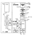
図4は、パチンコ遊技機1の制御回路を説明するためのブロック図である。図4には、制御基板として、遊技制御基板(主基板)31と、ランプ制御基板35と、賞球制御基板37と、音声制御基板70と、表示制御基板80と、発射制御基板91とが示されている。
【0045】
遊技制御基板31、賞球制御基板37、ランプ制御基板35、音声制御基板70、発射制御基板91および表示制御基板80には、マイクロコンピュータ等が搭載されている。各制御基板31,37,35,70,80では、パチンコ遊技機1の電源の投入時に、制御基板に設けられたRAM内のデータを初期化する等の初期化処理が行なわれ、賞球制御基板37、ランプ制御基板35、音声制御基板70、表示制御基板80は、初期化処理が終了した時点で、遊技制御基板31からのコマンドを有効に受付け可能となる。
【0046】
遊技制御基板31は、パチンコ遊技機1の遊技制御を司る遊技制御用マイクロコンピュータ(以下、遊技制御用マイコンと略す)53が搭載された基板であり、他の制御基板35,37,70,80は遊技制御基板31から各々に出力される制御コマンド(ランプ制御コマンド、賞球制御コマンド、音声制御コマンド、表示制御コマンド)に基づいた制御動作を実行する。これらの制御コマンドのうち、ランプ制御コマンドと音声制御コマンドと表示制御コマンドについては共通化された共通コマンドがあり、この共通コマンドについては、遊技制御基板31から各制御基板35,70,80に対して同一時期に出力される。
【0047】
遊技制御基板31から制御コマンドが出力される場合には、それに伴って、コマンドの有効期間を示すINT信号(ストローブ信号)が出力される。INT信号は、無効状態では信号がハイレベル(オフ状態)となり、有効状態では信号がロウレベル(オン状態)となる。
【0048】
遊技制御基板31には、遊技制御用マイコン53の他、各スイッチからの信号を遊技制御用マイコン53に与えるスイッチ回路58と、ソレノイド16,21を遊技制御用マイコン53からの指令に従って駆動するソレノイド回路59と、電源投入時に遊技制御用マイコン53をリセットするための初期リセット回路63と、遊技制御用マイコン53から与えられるアドレス信号をデコードしてI/Oポート部(図示省略)のうちのいずれかの1/Oポートを選択するための信号を出力するアドレスデコード回路67と、遊技制御用マイコン53から与えられるデータに従って大当りの発生を示す大当り情報、可変表示装置8の始動回数を示す始動情報、確率変動が生じたことを示す確変情報をホール管理コンピュータなどのホストコンピュータに対して出力する情報出力回路64を含む。なお、さらに、遊技制御基板31には、図15を用いて後述するように、電源電圧を監視する電源監視手段が設けられている。
【0049】
遊技制御用マイコン53は、遊技制御用のプログラムなどを記憶するROM54と、ワークメモリとして使用されるRAM55と、遊技制御用のプログラムに従って制御動作を行なうCPU56とを含む。これらのうち、RAM55については、電源基板910からのバックアップ用電源によってバックアップされており、不意に停電が発生しても所定時間はそのRAMデータが保持される。
【0050】
スイッチ回路58には、ゲートスイッチ12、始動口スイッチ17、カウントスイッチ23、Vカウントスイッチ22、入賞球検出スイッチ99などが接続されており、これらの各スイッチからの検出信号がスイッチ回路58を介して遊技制御用マイコン53に入力される。
【0051】
賞球制御基板37には玉払出装置97やカードユニット50が接続されている。賞球制御基板37は遊技制御基板31から出力される賞球制御コマンドに基づいて玉払出装置97を駆動し賞球を払出す制御を行なう。さらに賞球制御基板37は、カードユニット50から出力される制御信号に基づいて貸玉を払出す制御を行なう。
【0052】
音声制御基板72にはスピーカ27が接続されている。音声制御基板70は遊技制御基板31から出力される音声制御コマンドに基づき、スピーカ27から種々の効果音を出力させる制御を行なう。
【0053】
ランプ制御基板35には、遊技効果LED28aや遊技効果ランプ28b,28c、賞球ランプ51、玉切れランプ52、普通図柄用の可変表示器10、特別図柄用の始動記憶表示器18、普通図柄用の始動記憶表示器、装飾ランプ25、未払出賞球有りランプ29といった多数のランプ・LEDが接続される。ただし、図4ではこれらの接続状況の図示は省略している。ランプ制御基板35は遊技制御基板31から出力されるランプ制御コマンドに基づいてこれらのランプ・LEDを制御する。
【0054】
表示制御基板80には、特別図柄用の可変表示装置8が接続される(図示省略)。表示制御基板80は、遊技制御基板31から出力される表示制御コマンドに従い可変表示装置8の可変表示部9に所定の画像を表示させる。
【0055】
発射制御基板91には駆動モータ94と操作ノブ(打球操作ハンドル)5とが接続されている。発射制御基板91は操作ノブ5の操作量に応じた速度で打球が打球発射装置(図示省略)から発射されるように、駆動モータ94を駆動制御する。
【0056】
図5は、表示制御基板80内の回路構成を、可変表示装置8で画像表示するためのCRT82および遊技制御基板31の出力ポート(ポートA,B)571,572および出力バッファ回路63とともに示すブロック図である。出力ポート571からは表示制御コマンドとして8ビット×2のデータが出力され、出力ポート572からは1ビットのINT信号(ストローブ信号)が出力される。
【0057】
表示制御用CPU101は、制御データROM102に格納されたプログラムに従って動作し、遊技制御基板31からノイズフィルタ107および入力バッファ回路105を介してINT信号が入力されると、入力バッファ回路105を介して表示制御コマンドを受信する。入力バッファ回路105として、たとえば、汎用ICである74HC244を使用することができる。なお、表示制御用CPU101がI/Oポートを内蔵していない場合は、入力バッファ回路105と表示制御用CPU101との間に、I/Oポートが設けられる。
【0058】
表示制御用CPU101は、受信した表示制御コマンドに従って、CRT82に表示される画面の表示制御を行なう。具体的には、表示制御コマンドに応じた指令をVDP103に与える。VDP103は、キャラクタROM86から必要なデータを読出す。VDP103は、入力したデータに従ってCRT82に表示するための画像データを生成し、その画像データをVRAM87に格納する。そして、VRAM87内の画像データは、R,G,B信号に変換され、トランジスタ508〜509を介してさらにアナログ信号に変換されてCRT82に出力される。
【0059】
なお、図5には、VDP103をリセットするためのリセット回路83、VDP103に動作クロックを与えるための発振回路85、および使用頻度の高い画像データ(人物、動物、または文字、図形もしくは記号などからなる画像)を格納するキャラクタROM86も示されている。
【0060】
さらに、図5に示された構成では、表示制御基板80において、リセットスイッチ110の出力が入力ポートに導入されている。表示制御用CPU101は、エラー発生後にリセットスイッチ110が押圧されたことを検出すると、制御をエラー発生前の状態に戻す。
【0061】
エラーとして、たとえば、遊技制御基板31から受信した表示制御コマンドが異常であった(未定義コマンドなど)場合などがある。表示制御用CPU101がエラー発生後でも表示制御コマンドを受信して記憶するように構成されていれば、リセットスイッチ110の押圧に基づいて、記憶している受信コマンドに基づく表示制御を行なうようにすることによって、エラー発生が遊技演出に及ぼす影響を小さくすることができる。
【0062】
入力バッファ回路105は、遊技制御基板31から表示制御基板80へ向かう方向にのみ信号を通過させることができる。したがって、表示制御基板80側から遊技制御基板31側に信号が伝わる余地はない。表示制御基板80内の回路に不正改造が加えられても、不正改造によって出力される信号が遊技制御基板31側に伝わることはない。なお、出力ポート571,572の出力をそのまま表示制御基板80に出力してもよいが、単方向にのみ信号伝達可能な出力バッファ回路63を設けることによって、遊技制御基板31が表示制御基板80への一方向性の信号伝達をより確実にすることができる。また、高周波信号を遮断するノイズフィルタ107として、たとえば3端子コンデンサやフェライトビーズが使用されるが、ノイズフィルタ107の存在によって、表示制御コマンドに基板間でノイズが乗ったとしても、その影響は除去される。
【0063】
また、図示のように、表示制御手段(可変表示制御手段)としての表示制御用CPU101は、遊技制御手段としてのCPU56が搭載された遊技制御基板31とは別の基板に搭載されている。これにより、遊技制御基板31のコンパクト化が図られている。
【0064】
図6は、遊技制御基板31における音声制御コマンドの信号送信部分および音声制御基板70の構成例を示すブロック図である。音声制御基板70には制御用CPU701、ROM711、RAM712等が設けられている。図示のように、音制御手段としての制御用CPU701は、遊技制御手段としてのCPU56が搭載された遊技制御基板31とは別の基板に搭載されている。これにより、遊技制御基板31のコンパクト化が図られている。
【0065】
この実施の形態では、遊技進行に応じて、遊技領域7の外側に設けられたスピーカ27の音声出力を指示するための音声制御コマンドが遊技制御基板31から音声制御基板70に出力される。図6に示すように、音声制御コマンドは、遊技制御用マイコン53における出力ポート(出力ポートC,D)573,574から出力される。出力ポート573からは制御コマンドデータとして8ビット×2のデータが出力され、出力ポート574からは1ビットのINT信号(ストローブ信号)が出力される。音声制御基板70において、遊技制御基板31からの各信号は、入力バッファ回路705を介して音声制御用CPU701に入力される。なお、音声制御用CPU701がI/Oポートを内蔵していない場合には、入力バッファ回路705と音声制御用CPU701との間に、I/Oポートが設けられる。
【0066】
たとえば、デジタルシグナルプロセッサによる音声合成回路702は、トランジスタ501〜506を介して受けた音声制御用CPU701の指示に応じた音声や効果音を発生し、音量切換回路703に出力する。音量切換回路703と、音声制御用CPU701の出力レベルを、設定されている音量に応じたレベルにして音量増幅回路704に出力する。音量増幅回路704は、増幅した音声信号をスピーカ27に出力する。
【0067】
入力バッファ回路705として、たとえば、汎用のCMOS−ICである74HC244が用いられる。74HC244のイネーブル端子には、常にローレベル(GNDレベル)が与えられている。よって、各バッファの出力レベルは、入力レベルすなわち遊技制御基板31からの信号レベルに確定している。よって、音声制御基板70側から遊技制御基板31側に信号が伝わる余地はない。したがって、音声制御基板70内の回路に不正改造が加えられたとしても、不正改造によって出力される信号が遊技制御基板31側に伝わることはない。なお、入力バッファ回路705の入力側にノイズフィルタを設けてもよい。
【0068】
また、遊技制御基板31側において、出力ポート574,575の外側にはバッファ回路67が設けられている。バッファ回路67として、たとえば、汎用のCMOS−ICである74HC244が用いられる。イネーブル端子には常にローレベル(GNDレベル)が与えられている。このような構成によれば、外部から遊技制御基板31の内部に入力される信号が阻止されるので、音声制御基板70から遊技制御基板31に信号が与えられる可能性がある信号ラインをさらに確実になくすことができる。
【0069】
さらに、図6に示された構成では、音声制御基板70において、リセットスイッチ710の出力が入力ポートに導入されている。音声制御用CPU701は、エラー発生後にリセットスイッチ710が押圧されたことを検出すると、制御をエラー発生前の状態に戻す。
【0070】
エラーとして、たとえば遊技制御基板31から受信した音声制御コマンドが異常であった場合(未定義コマンドなど)などがある。音声制御用CPU701がエラー発生後でも音声制御コマンドを受信して記憶するように構成されていれば、リセットスイッチ710の押圧に基づいて、記憶している受信コマンドに基づく音声制御を行なうようにすることによって、エラー発生が遊技演出に及ぼす影響を小さくすることができる。
【0071】
音声制御基板70のROM(図示省略)には、各種音声制御用のコマンドデータに応じた音声を音声合成回路(音声合成用LSI:たとえば、デジタルシグナルプロセッサ)702に発生させるための制御データが格納されている。音声制御用CPU701は、受信した各種音声制御コマンドデータに対応した制御データをROMから読出す。
【0072】
この実施の形態では、音声合成回路702は、転送リクエスト信号(SIRQ)、シリアルクロック信号(SICK)、シリアルデータ信号(SI)および転送終了信号(SRDY)によって制御される。音声合成回路702は、SIRQがローレベルになると、SICKに同期してSIを1ビットずつ取込み、SRDYがローレベルになるとそれまでに受信した各SIからなるデータを1つの音声再生用データと解釈する。なお、音声合成回路702は、SIによって制御データを受信すると、受信した制御データに応じた音声を発生する。
【0073】
図7は、遊技制御基板31およびランプ制御基板35における信号送受信部分を示すブロック図である。この実施の形態では、遊技効果LED28a、遊技効果ランプ28b,28c、賞球ランプ51、玉切れランプ52、可変表示器10、始動記憶表示器18、装飾ランプ25、未払出賞球有りランプ29等の点灯/消灯を指示するランプ制御コマンドが遊技制御基板31から出力される。
【0074】
ランプ制御基板35には、制御用CPU351、ROM352、RAM353およびトランジスタを含む回路600等が設けられている。図示のように、ランプ制御手段としての制御用CPU351は、遊技制御手段としてのCPU56が搭載された遊技制御基板31とは別の基板に搭載されている。これにより、遊技制御基板31のコンパクト化が図られている。
【0075】
ランプ制御コマンドは、遊技制御用マイコン53におけるI/Oポート部57の出力ポート(出力ポートE,F)575,576から出力される。出力ポート575は制御コマンドデータとしての8ビット×2ビットのデータを出力し、出力ポート576は1ビットのINT信号(ストローブ信号)を出力する。ランプ制御基板35において、遊技制御基板31から出力されるランプ制御コマンドが、入力バッファ回路355を介してランプ制御用CPU351に入力される。なお、ランプ制御用CPU351がI/Oポートを内蔵していない場合には、入力バッファ回路355とランプ制御用CPU351との間に、I/Oポートが設けられる。
【0076】
ランプ制御用CPU351は、各ランプ制御コマンドに応じて定義されているランプの点灯/消灯パターンに従い、各ランプ・LEDに対して点灯/消灯信号を出力する。なお、点灯/消灯パターンは、ROM352に記憶されている。
【0077】
入力バッファ回路355として、たとえば、汎用のCMOS−ICである74HC244が用いられる。74HC244のイネーブル端子には、常にローレベル(GNDレベル)が与えられている。よって、各バッファの出力レベルは、入力レベルすなわち遊技制御基板31からの信号レベルに確定している。したがって、ランプ制御基板35側から遊技制御基板31側に信号が伝わる余地はない。たとえ、ランプ制御基板35内の回路に不正改造が加えられたとしても、不正改造によって出力される信号が遊技制御基板31側に伝わることはない。たとえば、ランプ制御基板35において、遊技制御基板31の遊技制御用マイコン53に大当りを生じさせるための不正信号を与えるような改造を行なったとしても、不正信号を遊技制御基板31側に伝えることはできない。なお、入力バッファ回路355の入力側にノイズフィルタを設けてもよい。
【0078】
さらに、遊技制御基板31において、出力ポート575,576の外側にバッファ回路62が設けられている。バッファ回路62として、たとえば、汎用のCMOS−ICである74HC244が用いられる。イネーブル端子には常にローレベル(GNDレベル)が与えられている。このような構成によれば、外部から遊技制御基板31の内部に入力される信号が阻止されるので、ランプ制御基板35から遊技制御基板31に信号が与えられる可能性がある信号ラインをより確実になくすことができる。
【0079】
さらに、図7に示された構成では、ランプ制御基板35において、リセットスイッチ360の出力が入力ポートに導入されている。ランプ制御用CPU351は、エラー発生後にリセットスイッチ360が押圧されたことを検出すると、制御をエラー発生前の状態に戻す。
【0080】
エラーとして、たとえば遊技制御基板31から受信したランプ制御コマンドが異常であった(未定義コマンドなど)場合がある。ランプ制御用CPU351がエラー発生後でもランプ制御コマンドを受信して記憶するように構成されていれば、リセットスイッチ360の押圧に基づいて、記憶している受信コマンドに基づく表示制御を行なうことによって、エラー発生が遊技演出に及ぼす影響を小さくすることができる。
【0081】
なお、図7における、ランプ制御用CPU351の内蔵出力ポートと各ランプ・LEDとの間の回路600は、後述するトランジスタを含む回路511〜517,520,530,541,542,550,556である。
【0082】
図8は、賞球制御基板37および玉払出装置97の構成要素などの賞球に関連する構成要素を示すブロック図である。賞球制御基板37には、制御用CPU371と、ROM380と、RAM381と、I/Oポート372(372a〜372g)と、入力バッファ回路373と、エラー表示用LED374と、リセットスイッチ(リセットSW)379とが設けられている。このように、賞球制御手段(価値付与制御手段、または払出制御手段)としての制御用CPU371は、遊技制御手段としてのCPU56が搭載された遊技制御基板31とは別の基板に搭載されている。これにより、遊技制御基板31のコンパクト化が図られている。
【0083】
図8に示すように、各種入賞口に入賞した入賞玉を遊技盤裏面側の集合樋で一括して検出する入賞球検出スイッチ99と、満タンスイッチ48の検出信号は、中継基板71を介して遊技制御基板31のI/Oポート57に入力される。また、入賞球排出ソレノイド127は、遊技盤裏面の入賞球流下路の途中に設けられている玉止め部材を駆動するものであって、玉止め部材に入賞球が停止している状態で入賞球検出スイッチ99によって入賞球が検出される。なお、満タンスイッチ48は、特に、余剰玉受皿4の満タンを検出するスイッチである。
【0084】
玉切れ検出スイッチ167および玉切れスイッチ187(187a,187b)からの検出信号は、中継基板72および中継基板71を介して遊技制御基板31のI/Oポート57に入力される。玉切れ検出スイッチ167は景品玉タンク38内の補給玉の不足を検出するスイッチであり、玉切れスイッチ187は、景品玉通路内の景品玉の有無を検出するスイッチである。
【0085】
遊技制御基板31のCPU56は、玉切れ検出スイッチ167または玉切れスイッチ187からの検出信号が玉切れ状態を示しているか、または、満タンスイッチ48からの検出信号が満タン状態を示していると、球貸し禁止を指示する賞球制御コマンドを賞球制御基板37に対して送出する。賞球制御基板37の賞球制御用CPU371は、球貸し禁止を指示する賞球制御コマンドを受信すると、球貸し処理を停止する。
【0086】
さらに、賞球カウントスイッチ301Aからの検出信号も、中継基板72および中継基板71を介して遊技制御基板31のI/Oポート57に入力される。また、遊技制御基板31のI/Oポート57から入賞球排出ソレノイド127への駆動信号は、中継基板71を介して入賞球排出ソレノイド127に供給される。なお、賞球カウントスイッチ301Aは、玉払出装置97の賞球機構部分に設けられ、実際に払出された賞球を検出する。
【0087】
入賞があると、賞球制御基板37には、遊技制御基板31の出力ポート(ポートG,H)577,578から賞球個数を示す賞球制御コマンド(賞球個数コマンド)が出力される。出力ポート577は8ビット×2の制御コマンドデータを出力し、出力ポート578は1ビットのINT信号(ストローブ信号)を出力する。賞球個数を示す賞球制御コマンドは、入力バッファ回路373を介してI/Oポート372aに入力される。入力バッファ回路373における各バッファは、遊技制御基板31から賞球制御基板37へ向かう方向にのみ信号を通過させることができる。したがって、賞球制御基板37側から遊技制御基板31側に信号が伝わる余地はない。賞球制御基板37内の回路に不正改造が加えられても、不正改造によって出力される信号が遊技制御基板31側に伝わることはない。なお、入力バッファ回路373の入力側にノイズフィルタを設けてもよい。
【0088】
また、遊技制御基板31側において、賞球制御コマンドを出力する出力ポート577,578の外側にバッファ回路68が設けられている。このような構成によれば、外部から遊技制御基板31の内部に入力される信号が阻止されるので、賞球制御基板37から遊技制御基板31に信号が与えられる可能性がある信号ラインをより確実になくすことができる。
【0089】
また、賞球制御用CPU371は、出力ポート372gを介して、貸し玉数を示す球貸し個数信号をターミナル基板160に出力し、ブザー駆動信号をブザー基板75に出力する。ブザー基板75には図示しないブザーが搭載されている。さらに、出力ポート372eを介して、エラー表示用LED374にエラー信号を出力する。
【0090】
さらに、賞球制御基板37の入力ポート372bには、中継基板72を介して、賞球カウントスイッチ301Aの検出信号および球貸しカウントスイッチ301Bの検出信号が入力される。球貸しカウントスイッチ301Bは、実際に貸出された遊技球を検出する。賞球制御基板37からの払出モータ289への駆動信号は、出力ポート372cおよび中継基板72を介して玉払出装置97の賞球機構部分における払出モータ289に伝えられる。また、振分け用ソレノイド310を駆動するための信号が、出力ポート372dおよび中継基板72を介して振分け用ソレノイド310に伝えられる。
【0091】
また、図8に示された構成では、リセットスイッチ379の出力が入力ポート372bに導入されている。賞球制御用CPU371は、エラー発生後にリセットスイッチ379が押圧されたことを検出すると、制御をエラー前の状態に戻す。
【0092】
賞球制御用CPU371がエラー発生後でも賞球制御コマンドを受信して記憶するように構成されていれば、リセットスイッチ379の押圧に基づいて、記憶している受信コマンドに基づく賞球制御を行なうことによって、遊技者に与えられる不利益をなくすことができる。
【0093】
カードユニット50には、カードユニット制御用マイクロコンピュータ(図示省略)が搭載されている。残高表示基板74には、打球供給皿3の近傍に設けられている度数表示LEDや球貸しスイッチ、返却スイッチが接続される。
【0094】
残高表示基板74からカードユニット50には、遊技者に操作に応じて、球貸しスイッチ信号および返却スイッチ信号が賞球制御基板37を介して与えられる。
【0095】
賞球制御基板37のCPU371は、賞球カウントスイッチ301Aの検出信号をカウントすることによって、払出した賞球数を計数するとともに、球貸しカウントスイッチ301Bの検出信号をカウントすることによって、払出した貸玉数を計数する。
【0096】
さらに、CPU371は、賞球カウントスイッチ301Aおよび球貸しカウントスイッチ301Bの検出信号に基づいて玉を計数する動作と並行して、払出モータ位置センサ286からの検出信号を利用して、払出した賞球数および貸玉数を計数する。すなわち、玉払出装置97では、玉繰出し用のスクリュー288が180度だけ回転して払出モータ位置センサ286が1回ON/OFFするごとに玉が1つ払出されるように構成されているために、この払出モータ位置センサ286の出力信号の変化に基づいて払出した玉を間接的に検出し、玉数を計数するのである。
【0097】
なお、払出モータ位置センサ286に代えて、ステッピングモータである払出モータ289のステップパルス数を検出することで、スクリュー288の払出動作量(回転量)を検出し、これにより間接的に玉の払出しを検出するようにしてもよい。ただし、スクリュー288の回転を直接検出する払出モータ位置センサ286を用いる方が、精度の高い検出結果を得ることができるという利点がある。ステッピングモータのステップパルス数に基づいてスクリュー288の払出動作量(回転量)を検出する場合には1ステップ当りの制御量が何らかの要因で変化すると、検出される動作量に誤差が生じてしまうためである。
【0098】
ところで、払出モータ位置センサ286の出力信号に基づいて玉数を計数すると、スクリュー288からの玉の落下を待って検出信号が出力されるカウントスイッチ301A,301Bの出力信号に基づいて玉を計数するよりも迅速に計数動作を進めることができるが、スクリュー288内に整列された玉と玉との間に無用な隙間が空いていて、スクリュー288が半回転したときに玉が払出されなかった場合であっても玉が1つ払出されたものとみなされるという欠点がある。あるいは、球噛みその他の原因によって実際には玉が払出されなかった場合であっても玉が1つ払出されたものとみなされてしまう。
【0099】
このため、CPU371は、この払出モータ位置センサ286の出力信号に基づいて計数された玉数が払出予定数に達した後、一旦、スクリュー288の回転を止め、カウントスイッチ301A,Bの検出信号に基づいた計数結果を参照して、間違いなく予定通りの玉の払出しがあったか否かを確認し、払出数が不足する場合には、再度、スクリュー288を回転させて不足分の玉を払出す制御を行なう。
【0100】
このような2段階の制御をすることによって、払出モータ位置センサ286の検出出力に基づいて計数される玉(賞球または貸玉)の数が払出予定数に至るまでは、スクリュー288を高速回転させて連続的に玉を払出すことで、玉の払出しを迅速にすることができ、また、それにより払出しが不足するような場合でも、後にその不足分の払出しを行なうことよって払出しを正確にすることができる。
【0101】
賞球制御基板37から発射制御基板91には、打玉の発射状態を制御するための発射制御信号が与えられる。発射制御基板91においては、発射制御信号がLOWレベルである場合に、打玉の発射が禁止され、打玉の発射が不可能な状態に制御される。一方、発射制御信号がHIGHレベルである場合には、打玉の発射が許容され、打玉の発射が可能な状態に制御される。
【0102】
また、カードユニット50から残高表示基板74には、プリペイドカードの残高を示すカード残高表示信号および球貸し可表示信号が賞球制御基板37を介して与えられる。カードユニット50と賞球制御基板37との間では、ユニット操作信号(BRDY信号)、球貸し要求信号(BRQ信号)、球貸し完了信号(EXS信号)およびパチンコ機動作信号(PRDY信号)がI/Oポート372fを介してやり取りされる。
【0103】
パチンコ遊技機1の電源が投入されると、賞球制御基板37の賞球制御用CPU371は、カードユニット50にPRDY信号を出力する。カードユニット50においてカードが受け付けられ、球貸しスイッチが操作され球貸しスイッチ信号が入力されると、カードユニット制御用マイクロコンピュータは、賞球制御基板37にBRDY信号を出力する。この時点から所定の遅延時間が経過すると、カードユニット制御用マイクロコンピュータは、賞球制御基板37にBRQ信号を出力する。そして、賞球制御基板37の賞球制御用CPU371は、払出モータ289を駆動し、所定個数の貸玉を遊技者に払出す制御を行なう。このとき、賞球制御用CPU371は、振分け用ソレノイド310を制御し、玉振分け部材311を球貸し側に向ける。その後払出が完了すれば、賞球制御用CPU371は、カードユニット50にEXS信号を出力する。
【0104】
以上のように、カードユニット50からの信号はすべて賞球制御基板37に入力される構成となっている。したがって、球貸し制御に関して、カードユニット50から遊技制御基板31に信号が入力されることはなく、遊技制御基板31の遊技制御用マイコン53にカードユニット50側から不正に信号が入力される余地はない。なお、遊技制御基板31および賞球制御基板37には、ソレノイドやモータ、ランプを駆動するためのドライバ回路が搭載されているが、図8では、それらの回路は省略されている。
【0105】
この実施の形態では、遊技制御基板31のRAM55(図4参照)の他、少なくとも賞球制御基板37のRAM381は、電源基板910のバックアップ用電源でバックアップされている。このため、遊技機に対する電力供給が停止しても、バックアップ電源によって一定時間RAM55,381は記憶内容を保持することができる。
【0106】
ここで、上記のようなパチンコ遊技機1の各基板同士の間の接続を、電気回路図を用いて説明する。
【0107】
まず、電源基板910について説明する。図9に示すように、電源基板910には、上から順にランプ制御基板35に接続される配線Y、電源コードに接続される配線、主基板(遊技制御基板)31に接続される配線D、賞球制御基板(払出制御基板)37に接続される配線F、発射中継A基板に接続される配線G、払出制御基板に接続される配線E、主基板に接続される配線Aおよび音声制御基板70に接続される配線Xが設けられている。
【0108】
また、図10に示すように、配線Xが接続される音声制御基板70は主基板31からも配線Cが接続されている。音声制御基板70はさらに音声中継A基板に配線により接続されている。音声中継A基板は、音声中継B基板と音声中継C基板とに配線により接続されている。音声中継B基板および音声中継C基板それぞれは左右のスピーカ27にそれぞれ接続されている。
【0109】
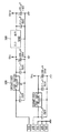
次に、音声制御基板70の内部の電気回路構造を、図11〜図16を用いて具体的に説明する。電源基板910から導入された配線1/5,2/5,3/5,4/5,5/5のうち配線3/5,4/5,5/5はアースされている。配線1/5は、後述するように、音声合成ICに電力を供給する配線であり、ノイズを除去するためのローパスフィルタ200、および、所定の電力を作成するためのレギュレータ300がそれぞれ接続されている。このレギュレータ300により12Vの電圧VDDが5Vの電圧AVccに降圧されて音声合成ICに電力が供給されている。
【0110】
このように、アナログ信号を処理する音声合成ICで使用する電圧AVccを、音声制御基板70内部の定電圧回路であるレギュレータ300において作成することにより、電源基板910から音声制御基板70まで伝達する間において発生するノイズによる悪影響を減少することができる。これにより、スピーカから発生される音声にノイズによる悪影響が生じることが低減される。
【0111】
また、図12に示すように、図10において主基板31から接続された配線Cは、それぞれ音声制御信号CD0〜CD7、音声制御信号INTが入力される配線およびGND(GRAND)線からなり、音声制御信号CD0〜CD7および音声制御信号INTが入力される配線それぞれは、不正な信号が主基板31側へ進入することを防止するためのバッファ回路705に接続されている。バッファ回路705からは、SCD0〜SDC7信号およびSINT信号が出力される。このSCD0〜SCD7信号およびSINT信号は、図13に示すように、音声を出力するための処理を行なう音声制御用CPU701に入力される。この音声制御用CPU701には、リセットスイッチ710が接続されている。また、音声制御用CPU701からはSICK信号,SI信号,SIRQ信号,SRDY信号,SRES信号それぞれが出力される。
【0112】
次に、図14に示すように、SICK信号,SI信号,SIRQ信号,SRDY信号,PRES信号それぞれは、トランジスタ501〜506それぞれに送られ、トランジスタ501〜506をONさせる。これにより、トランジスタ501〜506までの回路は電圧Vccによる系統の電源を用いていたが、トランジスタ501〜506以降の回路においては、電圧AVccによる系統の電源が用いられることになる。トランジスタ501〜506がONされたことによって生じた電力により、音声を合成するための信号を出力する音声合成IC702が駆動する。この音声合成IC702は、音声のデータが格納されている音声データROM711に接続されている。この音声データを用いて合成された音声データ信号がDAOR信号として音声合成ICから出力される。
【0113】
次に、図15に示すように、DAOL信号およびDAOR信号は、音のボリュームを調節するための音切換回路703を通過した後、音増幅回路704に到達して増幅されてスピーカ27に送り出される。
【0114】
上記のような本実施の形態によれば、音声制御用CPU701から音声合成IC702へのみ電気信号情報を伝達し、電流の逆流が生じないトランジスタ501〜506が設けられているため、スピーカ27で発生したノイズの悪影響が音声制御用CPU701に伝達されることが防止される。音声合成IC702が音声制御用CPU701に比較して大きな電力を消費する場合において、音声合成IC702での消費電力の変化が音声制御用CPU701に大きな悪影響を与えることが防止される。その結果、音声制御用CPU701は安定して駆動する。
【0115】
また、音声制御用CPU701がノイズの影響を比較的受け難いデジタル回路からなり、音声合成IC702がノイズの影響を受け易いアナログ回路含むため、上記トランジスタ501〜506によって音声合成IC702から音声制御用CPU701へのノイズの影響が伝達されることが防止されれば、電子回路全体は安定して駆動することができる。
【0116】
また、配線2/5より供給される電圧Vcc(+5V)の電力は音声制御用CPU701に供給され、配線1/5より供給される電圧12Vの電力から作成された電圧AVDD(+5V)の電力は音声合成IC702および音増幅回路704などに供給されるため、音声制御用CPU701の電源は音声合成IC702および音増幅回路704等の電源から独立することとなる。そのため、音増幅回路704等で消費される電力消費量の変化に関らず、音声制御用CPU701に安定した電力を供給することが可能となる。すなわち、音増幅回路704等の動作状態によっては、音声制御用CPU701への電力供給が不足する状態が生じる可能性があり、このような状態においては主基板31から出力された制御コマンドを正確に受取れない等の障害が生じ得るが、上記のような構造にすることにより、音声制御用CPU701において制御コマンドを正確に受取れない等の障害が発生することが防止される。
【0117】
次に、表示制御基板80に関係する電気回路構造を説明する。図16に示すように、表示制御基板80は、主基板31に接続されるとともに、普通図柄基板180、LCDモジュール280またはCRT82にそれぞれ接続されている。
【0118】
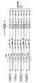
次に、表示制御基板80の内部の電気回路構造を、図17〜図26を用いて具体的に説明する。図17に示すように、主基板31から表示制御基板80に接続された配線のうち、配線10/16,11/16,12/16はアースされている。電圧Vccの電源に接続された13/16,14/16はノイズを除去するためのローパスフィルタ107に接続され、電圧Vcc(5V)の電源を供給している。電圧VDD(12V)の電源に接続された15/16,16/16は、ノイズを除去するためのローパスフィルタ108および所定の電力と作成するためのスイッチングレギュレータ109に接続されて電圧AVDD(5V)の電源を供給している。
【0119】
このように、CRT82またはLCD280等のアナログ信号を処理する回路で使用する電圧AVDDを、表示制御基板80の定電圧回路であるスイッチングレギュレータ300で作成することにより、電源基板910から表示制御基板80まで伝達する間において発生するノイズによる悪影響を減少することができる。これにより、CRT82またはLCD280に表示される映像にノイズによる悪影響が生じることが低減される。
【0120】
また、図18に示すように、配線1/16,2/16,3/16,4/16,5/16,6/16,7/16,8/16,9/16それぞれは、主基板31から図柄制御信号CD1〜CD7それぞれおよび図柄制御信号INTが入力される。図柄制御信号CD1〜CD7それぞれおよび図柄制御信号INTは、フェライトビーズFBによりノイズが除去された後、主基板31への信号の逆流を防止するためのバッファ回路105に入力される。バッファ回路105からはIN0信号〜IN7信号およびINT信号が出力される。
【0121】
次に、図19に示すように、このIN0〜IN7信号およびINT信号は、表示制御用CPU101に入力される。表示制御用CPU101には、図20に示す表示制御データROM102が接続されている。また、表示制御用CPU101には、図24に示すVDP103が接続され、VDP103には、図21および図22に示す計時用の水晶発振器を有する発振回路85、図23に示す回路を初期化するためのリセット回路83、図25に示すVRAM87、キャラクタROM86aおよびキャラクタROM86bそれぞれが接続されている。VDP103は、入力された信号に基づきキャラクタROM86aおよびキャラクタROM86bから画像データを読み出し後、画像データを生成してVRAM87に表示データとして格納する。その後、図26に示すように、VDP103は、VRAM87に格納された表示データをさらにRGB信号にして送り出す。このRGB信号によってトランジスタ508,509,510がONする。これにより、トランジスタ508,509,510までの回路は電圧Vccの電源により駆動しているが、トランジスタ508,509,510以降のCRT82またはLCDモジュール280の回路は電圧AVDDの電源により駆動することになる。
【0122】
上記のような本実施の形態によれば、VDP103からCRT82等へのみ電気信号情報を伝達し、電流の逆流が生じないトランジスタ508〜510が設けられているため、CRT82等で発生したノイズの悪影響がVDP103に伝達されることが防止される。CRT82がVDP103に比較して大きな電力を消費する場合において、CRT82での消費電力の変化がVDP103に大きな悪影響を与えることが防止される。その結果、VDP103は安定して駆動する。
【0123】
また、VDP103がノイズの影響を比較的受け難いデジタル回路からなり、CRT82がノイズの影響を受け易いアナログ回路を含むため、上記トランジスタ508〜510によってCRT82からVDP103へのノイズの影響が伝達されることが防止されれば、電子回路全体は安定して駆動することができる。
【0124】
また、配線13/16,14/16より供給される電圧Vcc(5V)の電力は表示制御用CPU101等に供給され、配線15/16,16/16より供給される電圧VDD(15V)の電力から作成された電圧AVcc(+5V)の電力はCRT82またはLCD280等に供給されるため、表示制御用CPU101の電源はCRT82等の電源から独立することとなる。そのため、CRT82等で消費される電力消費量の変化に関らず、表示制御用CPU101に安定した電力を供給することが可能となる。すなわち、CRT82等の動作状態によっては、表示制御用CPU101への電力供給が不足する状態が生じる可能性があり、このような状態においては主基板31から出力された制御コマンドを正確に受取れない等の障害が生じ得るが、上記のような構造にすることにより、表示制御用CPU101において制御コマンドを正確に受取れない等の障害が発生することが防止される。
【0125】
次に、ランプ制御基板35に関係する電気回路の構造を、図27〜図29を用いて説明する。図27に示すように、図9に示す電源基板910から引き出された配線Yはランプ制御基板35に接続されている。ランプ制御基板35には主基板35に接続される配線B、図28に示すランプ中継基板35aに接続される配線y1および図29に示される枠用ランプ中継A基板35hに接続される配線y2が設けられている。
【0126】
また、図28に示すように、ランプ中継A基板35aは、配線により、袖左基板35b、袖右基板35c、センター基板35d、AT右基板35e、AT中基板35fおよびAT左基板35gに接続されている。
【0127】
また、図29に示すように、ランプ中継A基板35hは、枠用ランプ中継B基板35i1および枠用ランプ中継C基板35i2に配線により接続されている。さらに、枠用ランプ中継B基板35i1には、前板ランプ左B基板35j、前板ランプ左A基板35k、前板ランプ上基板35l、前板ランプ右A基板35m、前板ランプ右B基板35nが配線を介して接続され、枠用ランプ中継C基板35i2には、スピーカLED左A基板35o、スピーカLED左B基板35p、スピーカLED右B基板35gおよびスピーカLED右A基板35rが配線を介して接続されている。
【0128】
次に、図30〜図36を用いて、ランプ制御基板35の内部構造について説明する。図30に示すように、電源基板910から導入された配線1/6,2/6,3/6,4/6,5/6,6/6のうち配線1/6からは、スイッチングレギュレータ700を介してが電圧VSLの電力が供給されている。また配線2/6は、電圧VLPの電力を供給している配線である。配線3/6からは、スイッチングレギュレータ800を介して電圧VDDの電力が供給されている。配線4/6からは、スイッチングレギュレータ900を介してVccが供給されている。配線5/6,6/6はアース(GND)されている。
【0129】
また、図31に示すように、ランプ制御基板35には、図16に示す主基板31から、ランプ制御信号CD0〜CD7が入力される配線1/11〜配線8/11、ランプ制御信号INTが入力される配線9/11およびGND配線10/11,11/11が接続され、ノイズを吸収するフェライトビーズを介して、ランプ制御CD0信号,ランプ制御信号CD1〜CD7信号それぞれは、信号の逆流を防止するバッファ回路355に入力される。バッファ回路355からはLCD0信号,LCD1信号〜LCD7信号が出力される。また、ランプ制御信号INTがインバータ回路を介してINT信号となり出力される。
【0130】
次に、図32に示すように、LCD0信号〜LCD7信号それぞれは、ランプの点灯消滅を制御するための信号を出力するCPU351に入力される。CPU351からは、BLANP(B)信号,BLANP(A)信号,BLED(F)信号,BLED(E)信号,BLED(D)信号,BLED(C)信号,BLED(B)信号,BLED(A)信号が出力される。また、CPU351からは、MMRY(a)信号,MMRY(b)信号,MMRY(c)信号,MMRY(d)信号、FLED(A)信号,FLED(B)信号,FLED(C)信号,FLED(D)信号が出力される。FLANP(A)信号,FLANP(B)信号,FLANP(C)信号,FLANP(D)信号,FLANP(E)信号,SLANP信号が出力される。さらに、CPU351からは、DG1信号,DG2信号およびTLANP信号が出力される。
【0131】
次に、図33に示すように、FLANP(A)信号,FLANP(B)信号,FLANP(C)信号,TLANP信号,FLANP(D)信号,SLANP信号,FLANP(E)信号ぞれぞれは、電流の逆流を防止する態様で設けられたトランジスタを含む回路511,512,513,514,515,516,517それぞれに入力される。
【0132】
その後、トランジスタを含む回路511,512,513,514,515,516,517から出力された信号は、右下枠ランプ(遊技効果ランプ28b,28cに相当)を制御するための信号を出力する配線1/18、右上枠ランプ(遊技効果ランプ28b,28cに相当)を制御するための信号を出力する配線2/18、天枠ランプ(遊技効果ランプ28b,28cに相当)を制御するための信号を出力する配線3/18、球切れランプ52を制御するための信号を出力する配線4/18、左上枠ランプ(遊技効果ランプ28b,28cに相当)を制御するための信号を出力する配線5/18、賞球ランプを制御するための信号を出力する配線6/18、左下枠ランプ(遊技効果ランプ28b,28cに相当)を制御するための信号を出力する配線9/18から図29に示すアナログ回路を含む枠用ランプ中継基A板35hに出力される。また、電圧VLPの電力は配線7/18,8/18に分かれて枠用ランプ中継A基板35hに出力される。
【0133】
また、図34に示すように、FLED(A)信号,FLED(B)信号,FLED(C)信号,FLED(D)信号は、電流の逆流を防止する態様で設けられたトランジスタを含むインバータ回路521,522,523,524,525,526,527,528を介して、配線11/18,12/18,13/18,14/18,15/18,16/18,17/18,18/18から遊技効果LED28aに相当する左スピーカ外LED、左スピーカ内LED、右スピーカ内LED、右スピーカ外LEDそれぞれを制御するために、枠用ランプ中継A基板35hに出力される。また、交流電源ACの電圧24Vの電力を整流し平滑した電圧VSLの電力が10/18から枠用ランプ中継A基板35hに供給される。
【0134】
また、図35に示すように、BLED(A)信号,BLED(B)信号,BLED(C)信号,BLED(D)信号,BLED(E)信号,BLED(F)信号それぞれは、電流の逆流を防止する態様で設けられたトランジスタを含むインバータ回路531,532,533,534,535,536,537,538を介して遊技効果LED25aに相当する飾りLEDを制御するための配線3A,2A,1A,6B,10B,7B,9B,8Bから図28に示すランプ中継基板35aに出力される。また、上記電圧VSLの電力が配線4B,5B,4Aから供給されている。BLANP(A)信号およびBLANP(B)信号それぞれは、電流の逆流を防止する態様で設けられたトランジスタを含む回路541,542を介して、装飾ランプ25に相当する飾りランプA,Bを制御するために配線2B,3Bから出力される。
【0135】
また、図36に示すように、MMRY(a)信号,MMRY(b)信号,MMRY(c)信号,MMRY(d)信号は、電流の逆流を防止する態様で設けられたトランジスタを含むインバータ回路551,552,553,554を介して、始動記憶表示器18に相当するLED1,LED2,LED3およびLED4を制御するために、配線10A,9A,8A,7Aから図28に示すランプ中継基板35aに出力される。また、DG1信号およびDG2信号は電流の逆流を防止する態様で設けられたトランジスタを含むバッファ回路555,556を介して配線6A,5Aからランプ中継基板35aに出力される。また、電圧VLPの電力が配線1Aにより供給されている。
【0136】
また、配線1/6より供給される電圧VSL(30V)の電力は各種ランプ等に供給され、配線4/6より供給される電圧VDD(5V)の電力はランプ制御用のCPU351等に供給されるため、ランプ制御用のCPU351の電源は各種ランプ等の電源から独立することとなる。そのため、各種ランプ等で消費される電力消費量の変化に関らず、ランプ制御用のCPU351に安定した電力を供給することが可能となる。すなわち、各種ランプ等の動作状態によっては、ランプ制御用のCPU351への電力供給が不足する状態が生じる可能性があり、このような状態においては主基板31から出力された制御コマンドを正確に受取れない等の障害が生じ得るが、上記のような構造にすることにより、ランプ制御用CPU351において制御コマンドを正確に受取れない等の障害が発生することが防止される。
【0137】
また、配線10A〜7Aは、特別図柄の始動記憶表示器と普通図柄の始動記憶表示器との双方を制御するために使用される。すなわち、DG1信号が能動状態となっている場合には、普通図柄の始動記憶表示器が制御され、DG2信号が能動状態となっている場合には、特別図柄の始動記憶表示器が制御される。
【0138】
上記のような構造のランプ制御基板35によれば、図33に示すトランジスタを含む回路511,512,513,514,515,516,517、図34に示すトランジスタを含むインバータ回路521,523,524,525,526,527,528、図35に示すトランジスタを含むインバータ回路531,533,534,535,536,537,538およびトランジスタを含む回路541,542、図36に示すトランジスタを含むインバータ回路551,552,553,554およびトランジスタを含むバッファ回路555,556を備えているため、電流の逆流が防止される。その理由は、上記トランジスタを含む回路それぞれまでは、電圧Vccの電力が供給され、トランジスタを含む回路以降は電圧VSLおよび電圧VLPの電力が供給されているからである。それにより、ノイズが発生し易いアナログ回路を有する図28に示すランプ中継基板35aおよびアナログ回路を有する図29に示す枠用ランプ中継A基板35hからのノイズによる悪影響が、ランプ制御基板35内部のデジタル回路であるCPU35までの回路に伝達されることが防止される。
【0139】
なお、上記図5のブロック図においては、VDP103とCRT280(LCD280)との間にのみトランジスタ508〜510を設けた実施の形態を示したが、図37に示すように、表示制御用CPU101とVDP103との間にトランジスタ500を有する表示制御基板80であれば、アナログ信号を出力するVDP103とデジタル信号を出力する表示制御用CPU101との間の電流の逆流を防止することができるため、デジタル回路のみで構成された表示制御用CPU101までのデジタル回路が、VDP103以降のアナログ回路において発生し易いノイズの悪影響を受けることが防止される。
【0140】
また、図38には、図16に示す主基板31が電源基板910から電源を取り込んだ直後の電源入力回路が示されている。図38に示すように、主基板の電源入力回路は、各種のバイパスコンデンサ、平滑コンデンサおよびノイズフィルタ31a,31b,31cを経て、電源基板910において作成された電力、すなわち、電圧VSL,VDD,Vcc,VBBをそのまま取り込み、各IC等に出力している。すなわち、主基板31においては、各IC等において使用する電力の電圧を調整するための電力作成手段を設ける必要がないため、電力作成手段を設けていない。
【0141】
なお、上記のランプ基板35においては、電源基板910で作成された電圧VSL(30V)を用いて各種ランプに電源を供給したが、ランプ制御基板35内部に定電圧回路であるスイッチングレギュレータを設けて新たな電力を作成してもよい。このようにすれば、電源基板910からランプ制御基板35まで伝達する間において発生するノイズによる悪影響を減少することができるため、各種ランプに現れるノイズによる悪影響が低減される。
【0142】
上記のような本実施の形態のパチンコ遊技機によれば、表示制御基板80、音声制御基板70およびランプ制御基板35には主基板31から電力が供給されるため、電源基板910に、電源基板910と表示制御基板80、音声制御基板70、ランプ制御基板35それぞれと接続するためのコネクタを設ける必要がなくなる。それにより、電源基板910に設けるコネクタの数を低減することができるため、電源基板910の構造が簡単となる。
【0143】
また、本実施の形態のパチンコ遊技機によれば、電源基板910と表示制御基板80とを接続するためのコネクタを電源基板910に設ける必要がなくなる。それにより、機種変更にともない可変表示器10および表示制御基板80を必要としなくなる場合において、電源基板910に未接続のコネクタが存在しなくなる。その結果、未接続のコネクタが存在することによって生じる、電源基板910の未接続のコネクタから不正制御を行なうための情報が入力されるおそれがなくなる。したがって、機種変更にともなって生じる不正制御を予め防止するような構造にすることができる。
【0144】
また、本実施の形態のパチンコ遊技機によれば、表示制御基板80、音声制御基板70およびランプ制御基板35それぞれは、電力供給手段から供給された電力を利用して、電気部品の制御に必要な電力を作成する電力作成手段としてスイッチグレギュレータ109等を有しているため、外部に必要な電力を作成する電力作成手段を設ける必要がなくなる。
【0145】
図39は、電源監視および電源バックアップのためのCPU56周りの一構成例を示すブロック図である。図39に示すように、第1の電源監視回路(電源監視手段、または、第1の電源監視手段)からの電圧低下信号が、CPU56のマスク不能割込端子(NMI端子)に接続されている。第1の電源監視回路は、遊技機が使用する各種直流電流のうちいずれかの電源の電圧を監視して電源電圧低下を検出する回路である。この実施の形態では、第1の電源監視回路は、VSLの電源電圧を監視して、その電圧値が所定値以下になるとローレベルの電圧低下信号を発生する。電源電圧VSLは、遊技機で使用される直流電圧のうちで最大のものであってこの例では、+30Vである。したがって、CPU56は、割込処理によって電源断、または、電源低下の発生を確認することができる。なお、この実施の形態では、第1の電源監視回路は、後述する電源基板に搭載されている。
【0146】
図39には、システムリセット回路65も示されているが、この実施の形態では、システムリセット回路65は、第2の電源監視回路(第2の電源監視手段)も兼ねている。すなわち、リセットIC651は、電源投入時に、外付けのコンデンサ652と容量で決まる所定時間だけ出力をローレベルとし、所定時間が経過すると出力をハイレベルにする。すなわち、リセット信号をハイレベルに立上げてCPU56を動作可能状態にする。また、リセットIC651は、第1の電源監視回路が監視する電源電圧と等しい電源電圧である電源電圧VSLを監視して、電圧値が所定値(第1の電源監視回路が電圧低下信号を出力する電源電圧値よりも低い値)以下になるとローレベルの電圧低下信号を発生する。したがって、CPU56は、第1の電源監視回路からの電圧低下信号に応じて所定の電力供給停止時処理を行なった後、システムリセットされる。なお、この実施の形態では、リセット信号と第2の電源監視回路からの電圧低下信号とは同一の信号である。
【0147】
図39に示すように、リセットIC651からのリセット信号は、NAND回路947(論理積回路)に入力されるとともに、反転回路(NOT回路)944を介してカウンタIC941のクリア端子に入力される。カウンタIC941は、クリア端子への入力がローレベルになると、発振器943からのクロック信号をカウントする。そして、カウンタIC941のQ5出力がNOT回路945,946を介してNAND回路947に入力される。また、カウンタIC941のQ6出力は、フリップフロップ(FF)942のクロック端子に入力される。フリップフロップ942のD入力はハイレベルに固定され、Q出力は論理和回路(OR回路)949に入力される。OR回路949の他方の入力には、NAND回路947の出力がNOT回路948を介して導入される。そして、OR回路949の出力がCPU56のリセット端子に接続されている。このような構成によれば、電源投入時に、CPU56のリセット端子に2回のリセット信号(ローレベル信号)が与えられるので、CPU56は、確実に動作を開始する。
【0148】
そして、たとえば、第1の電源監視回路の検出電圧(電圧低下信号を出力することになる電圧)を+22Vとし、第2の電源監視回路の検出電圧を+9Vとする。そのように構成した場合には、第1の電源監視回路と第2の電源監視回路とは、同一の電源の電圧VSLを監視するので、第1の電源監視回路が電圧低下信号を出力するタイミングと第2の電圧監視回路が電圧低下信号を出力するタイミングとの差を所望の所定時間に確実に設定することができる。所望の所定時間とは、第1の電源監視回路から発せられた電圧低下信号に応じて電力供給停止時処理を開始してから電力供給停止時処理が確実に完了するまでの期間である。
【0149】
この例では、第1の電源監視手段が検出信号を出力することになる第1検出条件は+30V電源電圧が+22Vにまで低下したことであり、第2の電源監視手段が検出信号を出力することになる第2検出条件は+30V電源電圧が+9Vにまで低下したことにである。ただし、ここで用いられている電圧値は一例であって、他の値を用いてもよい。
【0150】
ただし、監視範囲が狭まるが、第1の電圧監視回路および第2の電圧監視回路の監視電圧として+5V電源電圧を用いることも可能である。その場合にも、第1の電圧監視回路の検出電圧は、第2の電圧監視回路の検出電圧よりも高く設定される。
【0151】
CPU56等の駆動電源である+5V電源から電力が供給されていない間、RAMの少なくとも一部は、電源基板から供給されるバックアップ電源によってバックアップされ、遊技機に対する電源が遮断しても内容は保存される。そして、+5V電源が復旧すると、システムリセット回路65からリセット信号が発せられるので、CPU56は、通常の動作状態に復帰する。そのとき、必要なバックアップ記憶情報が保存されているため、停電等からの復旧時に停電が発生した時点の遊技状態に復帰することができる。
【0152】
なお、図39では、電源投入時にCPU56のリセット端子に2回のリセット信号(ローレベル信号)が与えられる構成が示されたが、リセット信号の立上がりタイミングが1回しかなくても確実にリセット解除されるCPUを使用する場合には、符号941〜949で示された回路素子は不要である。その場合、リセットIC651の出力がそのままCPU56のリセット端子に接続される。
【0153】
また、リセットIC651の外付けコンデンサ652の容量により規定される遅延時間は、電源基板910からの電源供給が開始し、各基板(音声制御基板70、ランプ制御基板35、表示制御基板80、払出制御基板37)が完全に起動するのに十分な時間を担保している。これにより、遊技制御手段のCPU56が制御コマンドを出力した時点で出力対象の基板が動作しておらず、コマンドに応じた制御ができないという不都合が解消される。
【0154】
また、外付けコンデンサ652の他、リセットIC651から出力された信号を、CPU56に伝送する信号線の途中に遅延回路を設けて、CPU56の処理の開始時に待機処理を行なってもよい。また、電源基板910に各基板のシステムリセットを管理する手段を設け、電源基板910側で立上げ順を管理してもよい。
【0155】
また、上記システムリセット回路65は、電力供給開始時にCPUに対してシステムリセット信号を出力する初期リセット回路と、電圧の低下を検出してCPUの動作を停止される電源監視回路とからなる構成としてもよい。
【0156】
図40は、遊技機の電源基板910の一構成例を示すブロック図である。電源基板910は、主基板31、表示制御基板80、音声制御基板70、ランプ制御基板35および払出制御基板37等の電気部品制御基板と独立して設置され、遊技機内の各電気部品制御基板および機構部品が使用する電圧を生成する。この例では、AC24V、DC+30V(VSL)、DC+21V、DC+12V(VDD)およびDC+5V(Vcc)を生成する。また、バックアップ電源となるコンデンサ916は、DC+5V(VBB)すなわち各基板上のIC等を駆動する電源のラインから充電される。
【0157】
トランス911は、交流電源からの交流電圧を24Vに変換する。AC24V電圧は、コネクタ915に出力される。また、整流回路912は、AC24Vから+30Vの直流電圧を生成し、DC−DCコンバータ913およびコネクタ915に出力する。DC−DCコンバータ913は、+21V、+12Vおよび+5Vを生成してコネクタ915に出力する。コネクタ915はたとえば中継基板に接続されて中継基板から各電気部品制御基板および機構部品に必要な電圧の電力が供給される。なお、トランス911の入力側には、遊技機に対する電源供給を停止したり開始したりするための電源スイッチが設置されている。
【0158】
DC−DCコンバータ913からの+5Vラインは分岐してバックアップ+5Vラインを形成する。バックアップ+5Vラインとグランドレベルとの間には大容量のコンデンサ916が接続されている。コンデンサ916は、遊技機に対する電力供給が遮断されたときの電気部品制御基板のバックアップRAM(電源バックアップされているRAMすなわち記憶内容保持状態となり得る記憶手段)に対して記憶状態を保持できるように電力を供給するバックアップ電源となる。また、+5Vラインとバックアップ+5Vラインとの間に、逆流防止用のダイオード917が挿入される。
【0159】
なお、バックアップ電源として、+5V電源から充電可能な電池を用いてもよい。電池を用いる場合には、+5V電源から電力供給されない状態が所定時間継続すると容量がなくなるような充電池が用いられる。
【0160】
また、電源基板910には、上述した第1の電源監視回路を構成する電源監視用IC902が搭載されている。電源監視用IC902は、電源電圧VSLを導入し、電源電圧VSLを監視することによって電源断の発生を検出する。具体的には、電源電圧VSLが所定値(この例では+22V)以下になると、電源断または電圧低下が生ずるとして電圧低下信号を出力する。なお、監視対象の電源電圧は、各電気部品制御基板に搭載されている回路素子の電源電圧(この例では+5V)よりも高い電圧であることが好ましい。この例では、交流から直流に変換された直後の電圧VSL(+30V)が用いられている。電源監視用IC902からの電圧低下信号は、主基板31や払出制御基板37等の各種制御基板に供給される。
【0161】
電源監視用IC902が電源断または電圧低下を検知するための所定値は、通常時の電圧より低いが、各電気部品制御基板上のCPUがしばらくの間動作し得る程度の電圧である。また、電源監視用IC902が、CPU等の回路素子を駆動するための電圧(この例では+5V)よりも高く、また、交流から直流に変換された直後の電圧を監視するように構成されているので、CPUが必要とする電圧に対して監視範囲を広げることができる。したがってより精密な監視を行なうことができる。さらに、監視電圧としてVSL(+30V)を用いる場合には、遊技機の各種スイッチに供給される電圧が+12Vであることから、電源断時のスイッチオン誤検出の防止も期待できる。すなわち、+30V電源の電圧を監視すると、+30V作成の以降に作られる+12Vが落ち始める以前の段階でそれの低下を検出できる。よって、+12V電源の電圧が低下するとスイッチ出力がオン状態を呈するようになるが、+12Vより速く低下する+30V電源電圧を監視して電源断を認識すれば、スイッチ出力がオン状態を呈する前に電源復旧待ちの状態に入ってスイッチ出力を検出しない状態となることができる。
【0162】
また、電源監視用IC902は、電気部品制御基板とは別個の電源基板910に搭載されているので、第1の電源監視回路から複数の電気部品制御基板に電圧低下信号を供給することができる。電圧低下信号を必要とする電気部品制御基板がいくつあっても、第1の電源監視手段は1つ設けられればよいので、各電気部品制御基板における各電気部品制御手段が後述する復帰制御を行なっても、遊技機のコストはさほど向上しない。
【0163】
なお、図40に示された構成では、電源監視用IC902の検出出力(電圧低下信号)は、バッファ回路918,919を介してそれぞれ電気部品制御基板(たとえば主基板31と払出制御基板37)に伝達されるが、たとえば、1つの検出出力を中継基板に伝達し、中継基板から各電気部品制御基板に同じ信号を分配する構成でもよい。また、電圧低下信号を必要とする基板数に応じたバッファ回路を設けてもよい。
【0164】
次に、遊技機の動作について説明する。
図41は、主基板31におけるCPU56が実行するメイン処理を示すフローチャートである。遊技機に対する電源が投入されると、メイン処理において、CPU56は、まず、必要な初期設定を行なう(ステップS1)。
【0165】
そして、電源断時にバックアップRAM領域のデータ幅を処理(本例ではパリティデータの負荷等の停電発生NMI処理)が行なわれた否かの確認を行なう(ステップS2)。不測の電源断が生じた場合には、後述するようにバックアップRAM領域のデータを保護するための処理が行なわれている。そのような保護処理が行なわれていた場合をバックアップありとする。バックアップなしという確認結果であれば、初期処理を実行する(ステップS2,S3)。なお、本例では、バックアップRAM領域にバックアップデータがあるか否かは、電源断時にバックアップRAM領域に設定されるバックアップフラグの状態によって確認する。本例では、バックアップフラグ領域に「55H」が設定されていればバックアップあり(オン状態)を意味し、「55H」以外の値が設定されていればバックアップなし(オフ状態)を意味する。
【0166】
バックアップRAM領域にバックアップデータがある場合には、この実施の形態では、CPU56は、バックアップRAM領域のデータチェック(この例ではパリティチェック)を行なう(ステップS4)。不測の電源断が生じた後に復旧した場合には、バックアップRAM領域のデータが保存されていたはずであるから、チェック結果は正常になる。チェック結果が正常でない場合は、内部状態を電源断時の状態に戻すことができないので、停電復旧時でない電源投入時に実行される初期化処理を実行する(ステップS5,S3)。
【0167】
チェック結果が正常であれば、CPU56は、内部状態を電源断時の状態に戻すための遊技状態復旧処理を行なう(ステップS6)。したがって本例では、図42に示すように、バックアップフラグの値が「55H」に設定されており、かつ、チェック結果が正常である場合に、ステップS6の遊技状態復旧処理に移行する。そして、バックアップRAM領域に保存されていたPC(プログラムカウンタ)の指すアドレスに復帰する(ステップS7)。
【0168】
通常の初期化処理の実行(ステップS2,S3)を終えると、CPU56により実行されるメイン処理はタイマ割込フラグの監視(ステップS9)の確認が行なわれるループ処理に移行する。なお、ループ内では、表示用乱数更新処理(ステップS8)も実行される。
【0169】
なお、この実施の形態では、ステップS2でバックアップデータの有無を確認した後、バックアップデータが存在する場合にステップS4でバックアップ領域のチェックを行なうようにしていたが、逆に、バックアップ領域のチェック結果が正常であったことを確認した後、バックアップデータの有無の確認を行なうようにしてもよい。また、バックアップデータの有無の確認、または、バックアップ領域のチェックのいずれか一方の確認を行なうことで、停電復旧処理を実行するか否かを判別する構成としてもよい。
【0170】
通常の初期化処理では、図43に示すように、RAMのクリア処理が行なわれる(ステップS3a)。次いで、作業領域初期設定テーブルのアドレス値に基づいて、所定の作業領域(たとえば、普通図柄判定用乱数カウンタ、普通図柄判定用バッファ、特別図柄左中右図柄バッファ、払出コマンド格納ポインタなど)に初期値を設定する初期値設定処理(ステップS3b)が行なわれる。そして、2ms毎に定期的にタイマ割込がかかるようにCPU56に設けられているタイマレジスタの初期設定(タイムアウトが2msであることと、繰返しタイマが動作する設定)が行なわれる(ステップS3c)。すなわち、ステップS3cで、タイマ割込を能動化する処理と、タイマ割込インターバルを設定する処理とが実行される。そして、初期設定処理(ステップS1)において割込禁止(図45参照)とされているため、初期化処理を終える前に割込が許可される(ステップS3d)。
【0171】
したがって、この実施の形態では、CPU56の内部タイマが繰返しタイマ割込を発生するように設定される。この実施の形態では、繰返し周期は2msに設定される。そして、図44に示すように、タイマ割込が発生すると、CPU56は、タイマ割込フラグを設定する(ステップS12)。
【0172】
CPU56は、ステップS9において、タイマ割込フラグがセットされたことを検出すると、タイマ割込フラグをリセットするとともに(ステップS10)、遊技制御処理を実行する(ステップS11)。以上の制御によって、この実施の形態では、遊技制御処理は2ms毎に起動されることになる。なお、この実施の形態ではタイマ割込処理はフラグセットのみがなされ、遊技制御処理はメイン処理において実行されるが、タイマ割込処理での遊技制御処理を実行してもよい。
【0173】
上述したように、バックアップデータの有無により電源断時の状態に復旧するか否かの判別を行なうようにしたことで、停電後の電源復旧時などにおいて電源投入されたときに、バックアップデータ記憶領域の内容に応じて電源断時の状態に復旧させるか否かの判別を行なうことができる。したがって、バックアップデータに基づく制御を実現することができるとともに、不必要な復旧処理の実行を防止することができる。
【0174】
また、バックアップデータの状態により電源断時の状態に復旧するか否かの判別を行なうようにしたことで、停電後の電源復旧時などにおいて電源投入されたときに、バックアップデータ記憶領域の内容の状態に応じて電源断時の状態に復旧されるか否かの判別を行なうことができる。したがって、正常なバックアップデータに基づく制御を実現することができるとともに、異常が発生しているバックアップデータに基づく復旧処理の実行を防止することができる。
【0175】
図45は、ステップS1の初期設定処理を示すフローチャートである。初期設定処理において、CPU56は、まず、割込禁止に設定する(ステップS1a)。割込禁止に設定すると、CPU56は、割込モードを割込モード2に設定し(ステップS1b)、スタックポインタにスタックポインタ指定アドレスを設定する(ステップS1c)。そして、CPU56は、内蔵デバイスレジスタの初期化(ステップS1d)、前述の割込モード2に設定することにより使用が可能となるCTC(カウンタ/タイマ)およびPIO(パラレル入出力ポート)の初期化(ステップS1e)を行なった後、電源断時にRAMの内容を保護するためにRAMへのアクセスを不能としているため、RAMをアクセス可能状態に設定する(ステップS1f)。
【0176】
なお、初期設定処理において設定され得るINT信号の入力により割込が許可されるマスカブル割込の割込モードには、以下の3種類のモードがある。
【0177】
割込モード0:リセット時に設定されるモードであって、1バイトのCALL命令であるRST命令により割込元から指定されたアドレス(00(H)〜38(H))が、割込処理プログラムのスタートアドレスを示すモードである。
【0178】
割込みモード1:割込処理プログラムのスタートアドレス(38(H))が予め定められているモードである。
【0179】
割込みモード2:CPU56の特定レジスタの値(1バイト)と内蔵デバイスが出力する割込ベクター(1バイト:最大ビット0)から構成されるアドレスが、割込番地を示すものである。すなわち割込番地は、上位アドレスが特定レジスタの値とされ、下位アドレスが割込ベクターとされた2バイトで示されるアドレスである。
【0180】
図46は、ステップS11の遊技制御処理を示すフローチャートである。遊技制御処理において、CPU56は、まず、スイッチ回路58を介して、ゲートセンサ12、始動口センサ17、カウントセンサ23および入賞口スイッチ19a,24aの状態を入力し、各入賞口や入賞装置に対する入賞があったか否かを判別する(スイッチ処理:ステップS21)。
【0181】
続いて、パチンコ遊技機1の内部に備えられている自己診断機能によって異常診断処理が行なわれ、その結果に応じて必要ならば警報が発せられる(エラー処理:ステップS22)。
【0182】
次に、遊技制御に用いられる大当り判定用乱数等の各判定用乱数を示す各カウンタを更新する処理を行なう(ステップS23)。CPU56は、さらに、停止図柄の種類を決定する乱数等の表示用乱数を更新する処理を行なう(ステップS24)。
【0183】
さらにCPU56は、特別図柄プロセス処理を行なう(ステップS25)。特別図柄プロセス制御では、遊技状態に応じてパチンコ遊技機1を所定の順序で制御するための特別図柄プロセスフラグに従って該当する処理が選び出されて実行される。そして、特別図柄プロセスフラグの値は、遊技状態に応じて各処理中に更新される。また、普通図柄プロセス処理を行なう(ステップS26)。普通図柄プロセス処理では、7セグメントLEDにより可変表示器10を所定の順序で制御するための普通図柄プロセスフラグに従って該当する処理が選び出されて実行される。そして、普通図柄プロセスフラグの値は、遊技状態に応じて各処理中に更新される。
【0184】
また、CPU56は、表示制御基板80に送り出される特別図柄制御コマンドや普通図柄信号コマンドをRAM55の所定の領域に設定する処理を行なった後に、特別図柄制御コマンドや普通図柄制御コマンドを出力する処理を行なう(特別図柄コマンド制御処理:ステップS27,普通図柄コマンド制御処理:ステップS28)。
【0185】
次いで、CPU56は、各種出力データの格納領域の内容を各出力ポートに出力する処理を行なう(データ出力処理:ステップS29)。なお、CPU56は、たとえばホール管理用コンピュータに出力される大当り情報、始動情報、確率変動情報などの出力データを格納領域に設定する出力データ設定処理などの他の処理も行なう。
【0186】
また、CPU56は、所定の条件が成立したときにソレノイド回路59に駆動指令を行なう(ステップS30)。ソレノイド回路59は、駆動指令に応じてソレノイド16,21を駆動し、可変入賞球装置19または開閉板22を開状態または閉状態とする。また、CPU56は、たとえば入賞口24等の各入賞口の検出に基づく賞球数の設定などを行なう(ステップS31)。すなわち、所定の条件が成立すると払出制御基板37に払出制御コマンドを出力する。払出制御基板37に搭載されている払出制御用CPU371は、払出制御コマンドに応じて玉払出装置97を駆動する。
【0187】
以上のように、メイン処理には遊技制御処理に移行すべきか否かを判別する処理が含まれ、CPU56の内部タイマが定期的に発生するタイマ割込に基づくタイマ割込処理で、遊技制御処理に移行すべきか否かを判別するためのフラグがセットされるので、遊技制御処理のすべてが確実に実行される。つまり、遊技制御処理のすべてが実行されるまでは、次回の遊技制御処理に移行すべきか否かの判定が行なわれないので、遊技制御処理中のすべての各処理が実行を完了することは保証されている。
【0188】
従来の一般的な遊技制御処理は、定期的に発生する外部割込によって、強制的に最初の状態に戻されていた。図46に示された例に則して説明すると、たとえば、ステップS31の処理中であっても、強制的にステップS21の処理に戻されていた。つまり、遊技制御処理中のすべての各処理が実行を完了する前に、次回の遊技制御処理が開始されてしまう可能性があった。
【0189】
なお、ここでは、主基板31のCPU56が実行する遊技制御処理は、CPU56の内部タイマの定期的に発生するタイマ割込に基づくタイマ割込処理でセットされるフラグに応じて実行されたが、定期的に(たとえば2ms毎)信号を発生するハードウェア回路を設け、その回路からの信号をCPU56の外部割込端子に導入し、割込信号によって遊技制御処理に移行すべきか否かを判定するためのフラグをセットするようにしてもよい。
【0190】
そのように構成した場合にも、遊技制御処理のすべてが実行されるまでは、フラグの判定が行なわれないので、遊技制御処理の中のすべての各処理が実行を完了することが保証される。
【0191】
図47は、電源基板910の電源監視回路からの電圧変化信号に基づくNMIに応じて実行される停電発生NMI処理の一例を示すフローチャートである。停電発生NMI処理において、CPU56は、まず、停電時などの電源断時直前の割込許可/禁止状態をバックアップするために、割込禁止フラグの内容をパリティフラグに格納する(ステップS41)。次いで、割込禁止に設定する(ステップS42)。停電発生NMI処理では、RAM内容の保存を確実にするためにチェックサムの生成処理を行なう。その処理中に他の割込処理が行なわれたのではチェックサムの生成処理が完了しないうちにCPUが動作し得ない電圧にまで低下してしまうことが考えられるので、まず、他の割込が生じないような設定がなされる。なお、停電発生NMI処理におけるステップS44〜S50は、電力供給停止処理の一例である。
【0192】
また、割込処理中では他の割込がかからないような使用のCPUを用いている場合には、ステップS42の処理は不要である。
【0193】
次いで、CPU56は、バックアップフラグが既にセットされているか否か確認する(ステップS42)。バックアップフラグが既にセットされていれば、以後の処理を行なわない。バックアップセットがセットされていなければ、以下の電力供給停止時処理を実行する。すなわち、ステップS44からステップS55の処理を実行する。
【0194】
まず、各レジスタの内容をバックアップRAM領域に格納するステップS44)。その後、バックアップフラグをセットする(ステップS45)。そしてバックアップRAM領域のバックアップチェックデータ領域に適当な初期値を設定し(ステップS46)、初期値およびバックアップRAM領域のデータについて順次排他的論理和をとった後反転し(ステップS47)、最終的な演算値をバックアップパリティデータ領域に設定する(ステップS48)。また、RAMアクセス禁止状態にする(ステップS49)。さらに、すべての出力ポートをオフ状態にする(ステップS50)。電源電圧が低下しているときには、各種信号線のレベルが不安定になってRAM内容が化ける可能性があるが、このようにRAMアクセス禁止状態にしておけば、バックアップRAM内のデータが化けることはない。
【0195】
続いて、CPU56は、ループ処理に入る。すなわち何らの処理もしない状態になる。したがって、図39に示されたリセットIC651からのシステムリセット信号によって外部から動作禁止状態にされる前に、内部的に動作停止状態になる。よって、電源断時に確実にCPU56は動作停止する。その結果、上述したRAMアクセス禁止の制御および動作停止制御によって、電源電圧が低下することに伴って生じる可能性がある異常動作に起因するRAMの内容破壊等を確実に防止することができる。
【0196】
なお、この実施の形態では、停電発生NMI処理では最終部でプログラムをループ状態にしたが、ホールト(HALT)命令を発行するように構成してもよい。
【0197】
また、レジスタの内容をRAM領域に格納した後にセットされるバックアップフラグは、上述したように、電源投入時において復旧すべきバックアップデータがあるか否か(停電からの復旧か否か)を判断する際に使用される。また、ステップS41からS50の処理は、CPU56がシステムリセット回路65からのシステムリセット信号を受ける前に完了する。換言すれば、システムリセット回路65からのシステムリセット信号を受ける前に完了するように、電圧監視回路の検出電圧の設定が行なわれている。
【0198】
この実施の形態では電力供給停止時処理開始時に、バックアップフラグの確認が行なわれる。そして、バックアップフラグが既に設定されている場合は電力供給停止時処理を実行しない。上述したように、バックアップフラグは、必要なデータのバックアップが完了し、その後電力供給停止時処理が完了したことを示すフラグである。したがって、たとえばリセット待ちのループ状態でならかの原因で再度NMIが発生したとしても、電力供給停止時処理が重複して実行されてしまうようなことはない。
【0199】
ただし、割込処理中では他の割込が入らないような仕様のCPUを用いている場合には、ステップS43の判断は不要である。
【0200】
図48は、バックアップパリティデータ作成方法の一例を説明するための説明図である。ただし、図48に示す例では、簡単のために、バックアップデータRAM領域のデータサイズを3バイトとする。電源電圧低下に基づく停電発生処理において、図48に示すように、バックアップチェックデータ領域に、初期データ(この例では00H)が設定される。次に、「00H」と「F0H」の排他的論理和がとられてその結果と「16H」の排他的論理和がとられる。さらに、その結果、「DFH」の排他的論理和がとられる。そして、その結果(この例では「39H」)を反転して得られた値(この例では「C6H」)がバックアップパリティデータ領域に設定される。
【0201】
電源が再投入されたときには、停電復旧処理においてパリティ診断が行なわれる。バックアップ領域の全データがそのまま保存されていれば、電源再投入時に、図48に示すようなデータがバックアップ領域に設定されている。
【0202】
ステップS4の処理において、CPU56は、停電発生NMI処理にて実行された処理と同様の処理を行なう。すなわち、バックアップチェックデータ領域に、初期データ(この例では00H)が設定され、「00H」と「F0H」の排他的論理和がとられ、その結果、「16H」の排他的論理和がとられる。さらに、その結果と「DFH」の排他的論理和がとられる。そして、その結果(この例では「39H」)を反転した最終演算結果を得る。バックアップ領域の全データがそのまま保存されていれば、最終的な演算結果は、「C6H」、すなわち、バックアップチェックデータ領域に設定されているデータと一致する。バックアップRAM領域内のデータにビット誤りが生じていた場合には、最終的な演算結果は「C6H」にはならない。
【0203】
よって、CPU56は、最終的な演算結果とバックアップチェックデータ領域に設定されているデータとを比較して、一致すればパリティ診断正常とする。一致しなければパリティ診断異常とする。
【0204】
以上のように、この実施の形態では、遊技制御手段には、遊技機の電源が断になっても、所定期間電源バックアップされる記憶手段(この例ではバックアップRAM)が設けられ、電源投入時に、CPU56(具体的にはCPU56が実行するプログラム)は、記憶手段がバックアップ状態にあればバックアップデータに基づいて遊技状態を回復させる遊技状態復旧処理(ステップS6)を行なうように構成されている。
【0205】
この実施の形態では、図40に示されたように電源基板910に電源監視回路が搭載され、図39に示されるように主基板31にシステムリセット回路65が搭載されている。そして、電源電圧が低下していくときに、システムリセット回路65がローレベルのシステムリセット信号を発生する時期は、電源監視回路(この例では電源監視用IC902)がローレベルのNMI割込信号を発生する時期よりも遅くなるように設定されている。さらに、システムリセット回路65からのローレベルのシステムリセット信号は、CPU56のリセット端子に入力されている。
【0206】
すると、CPU56は、電源監視手段(電源監視用IC902)からの電圧低下信号に基づいて停電発生処理(電力供給停止時処理)を実行した後にループ状態に入るのであるが、ループ状態において、リセット状態に入ることになる。すなわち、CPU56の動作が完全に停止する。+5V電源電圧値で以下においては、CPU56の正常な動作が担保できない(すなわち、動作の管理ができない状態が発生する)が、CPU56は正常に動作できる電源が供給されている状態でリセット状態になるので、不定データに基づいて異常動作をしてしまうことは防止される。
【0207】
このように、この実施の形態では、CPU56が、電源監視回路からの検出出力の入力に応じてループ状態に入るとともに、システムリセット回路65からの検出信号の入力に応じてシステムリセットされるように構成されている。したがって、電源断時に確実なデータ保存が行なわれ、遊技者に不利益がもたらされることが防止される。
【0208】
なお、この実施の形態では、電源監視用IC902と、システムリセット回路65は、同一の電源電圧を監視しているが、異なる電源電圧を監視してもよい。たとえば、電源基板910の電源監視回路が+30V電源電圧を監視し、システムリセット回路65が+5V電源電圧を監視してもよい。そして、システムリセット回路65がローレベルのシステムリセット信号を発生するタイミングは、電源監視回路がNMI割込信号を発生するタイミングに対して遅くなるように、システムリセット回路65のしきい値レベル(システムリセット信号を発生する電圧レベル)が設定される。たとえば、しきい値は4.25Vである。4.25Vは、CPU56が動作する通常の電圧値より低いが、CPU56がしばらくの間動作し得る程度の電圧である。なお、システムリセット回路65に設けられた遅延手段の遅延時間(本例では、コンデンサの容量)を調整して、システムリセット回路65がローレベルのシステムリセット信号を発生するタイミングを電源監視回路がNMI割込信号を発生するタイミングに対して遅らせるようにしてもよい。
【0209】
また、上記の実施の形態では、CPU56は、マスク不能割込端子(NMI端子)を介して電源基板からのNMI割込信号(電源監視手段からのNMI割込信号)を検知したが、NMI割込信号をマスク可能割込端子(IRQ端子)に導入してもよい。その場合には、割込処理(IRQ処理)で電力供給停止時処理が実行される。また、入力ポートを介して電源基板910からのNMI割込信号を検知してもよい。その場合には、メイン処理において入力ポートの監視が行なわれる。
【0210】
また、NMI割込信号に代えてIRQ端子を介して電源基板910からの割込信号を検知する場合に、メイン処理のステップS10における遊技制御処理の開始時にIRQ割込マスクをセットし、遊技制御処理の終了時にIRQ割込マスクを解除するようにしてもよい。そのようにすれば、遊技制御処理の開始前および終了後に割込がかかることになって、遊技制御処理が途中で中断されることはない。したがって、払出制御コマンドを払出制御基板37に送り出しているときなどに、コマンド送り出しが中断されてしまうようなことはない。よって、停電が発生するようなときでも払出制御コマンド等が確実に送り出しを完了する。
【0211】
また、この実施の形態では、停電発生処理(電力供給停止時処理)において、既にデータがバックアップされ電力供給停止時処理が既に実行されたことを示すバックアップフラグがセットアップされている場合には、電力供給停止時処理を実行しないように構成されている。電源がダウンする過程では、再度NMIが発生する可能性がある。すると、電源発生処理においてバックアップフラグの確認を行なわない場合には、再度発生したNMIによって再度電力供給停止時処理が実行される。最初に実行された電力供給停止時処理では、レジスタの内容をバックアップRAMに格納する処理が行なわれる(図46におけるステップS44参照)。最初に実行された正規の電力供給停止時処理後のリセット待ちの状態では、電源電圧は徐々に低下していくので、レジスタの内容が破壊される可能もある。すなわち、レジスタ値は、電源断が検出されたときの状態(最初にNMIが発生したとき)から変化している可能性がある。そのような状態で再度電力供給停止時処理が実行されると、電源断が検出されたときの状態のレジスタ値とは異なる値がバックアップRAMに格納されてしまう。すると、電源復旧時に実行される電源復旧処理において、電源断が検出されたときの状態のレジスタ値とは異なる値がレジスタに復旧されてしまう。その結果電源断時の遊技状態とは異なる遊技状態が再現されてしまう可能性が生ずる。
【0212】
以下、遊技状態復旧処理について説明する。
図49は、図41のステップS6に示された遊技状態復旧処理の一例を示すフローチャートである。この例では、CPU56は、バックアップRAMに保存されていた値を各レジスタに復元する(ステップS61)。そして、バックアップRAMに保存されていたデータに基づいて停電時の遊技状態を確認して復旧させる。すなわちバックアップRAMに保存されていたデータに基づいて、ソレノイド回路59を介してソレノイド16,21を駆動し、たとえば始動入賞口24等や開閉板22の開閉状態の復旧を行なう(ステップS62,S63)。また、電源断中でも駆動されていた特別図柄プロセスフラグおよび普通図柄プロセスフラグの値に応じて、電源断時の特別図柄プロセス処理の進行状況および普通図柄プロセス処理の進行状況に対応した制御コマンドを、表示制御基板80、ランプ制御基板35および音声制御基板70に送り出す(ステップS63)。
【0213】
以上のように、遊技状態復旧処理では、復元された内部状態に応じて、各種電気部品の状態復元が行なわれるとともに、表示制御基板80、ランプ制御基板35および音声制御基板70に対して、制御状態を電源断時の状態に戻すための制御コマンド(電源断時の制御状態を処理するための制御コマンド)が送り出される。そのような制御コマンドが、一般に、電源断前に最後に送り出された1つまたは複数の制御コマンドである。
【0214】
その結果、この実施の形態では、遊技状態復旧処理によって、以下のような状態復旧が可能である。始動入賞口14および大入賞口(開閉板)22の状態が復元される。表示制御手段によって制御される普通図柄の表示状態(可変表示器10の表示状態)は、電源断時に変動中であった場合を除いて復元される。表示制御手段によって制御される特別図柄の表示状態(可変表示部9の表示状態)は、電源断時に変動中であった場合を除いて復元される。さらに、可変表示部9に表示される背景やキャラクタは、特別図柄変動中および大当り遊技中であった場合を除いて復元される。
【0215】
特別図柄の変動中に電源断となった場合には、可変表示パターンの変動時間(たとえば10秒)および既に実行した時間(たとえば4秒)の情報がバックアップされる。そして、主基板31は、普及時に、表示パターンを示す表示制御コマンドおよび停止図柄を示す表示制御コマンドを表示制御基板80に出力し、残り時間(上述の例では6秒)経過後に、図柄を停止させるため表示制御コマンドを出力する。したがって、特別図柄の表示状態は、電源断時に特別図柄の変動中であった場合には、復旧時に、表示されていない残りの時間(上述の例では6秒)につき可変表示が実行される。なお、復旧時に表示制御基板80に対して出力される表示パターンを示す表示制御コマンドは、電源断前に出力された表示パターンを示す表示制御コマンドと同じものであってもよいが、「停電復旧中です」のような画像表示をさせるためのコマンドとしてもよい。この場合、「電源復旧中です」の表示は、残り時間(上述の例では6秒)表示される。なお、特別図柄の変動中に電源断となった場合の、普通図柄の表示状態に基づいても、上述と同様の制御が行なわれる。
【0216】
なお、大当り遊技中に電源断となった場合にも、上述した特別図柄の変動中に電源断となった場合と同様に、ラウンド中あるいはラウンド間のインターバルの残り時間について、復旧時に、表示、音、ランプ、ソレノイド16,21などを制御するが、主基板31は、表示制御基板80に対して電源断前に出力した確定時の図柄(停止図柄)を指定する表示制御コマンドを出力する。
【0217】
これにより、ラウンド中あるいはラウンド間の大当り図柄による演出が可能となり(大当り図柄で大当り演出する機種について)、また、大当り終了後の変動開始時に表示する図柄も表示制御基板80が認識することができる。
【0218】
ランプ制御手段が制御する装飾ランプ25、始動記憶表示器18、ゲート通過記憶表示器41、賞球ランプ51および玉切れランプ52の表示状態が復旧される。遊技効果ランプ・LED28a,28b,28cの表示状態は、特別図柄変動中および大当り遊技中であった場合を除いて復元される。ただし、電源断時に大当り遊技中であった場合には、各制御区間の最初の状態に復元可能である。各制御区間とは、たとえば、大当り開始保持状態、大入賞開放前状態、大入賞口開放中状態、大当り終了報知状態である。なお、特別図柄変動中に電源断となった後復旧した場合には、上述した可変表示部9や可変表示装置10の表示制御と同様に、残り時間分だけ遊技効果ランプ・LED28a,28b,28cの表示状態を制御するようにしてもよいが、消灯または停電復旧時特有のパターンで点灯・点滅するようにしてもよい。
【0219】
音声制御手段が制御する音声発生状態は、特別図柄変動中および大当り遊技中であった場合を除いて復元される。ただし、電源断時に大当り遊技中であった場合には、各制御区間の最初の状態に復元可能である。なお、特別図柄変動中に電源断となった後復旧した場合には、上述した可変表示部9や可変表示装置10の表示制御と同様に、残り時間分だけ音声発生状態を制御するようにしてもよいが、無音または停電復旧時特有の音声パターン(たとえば「停電復旧中です」との音声)を出力するようにしてもよい。
【0220】
なお、この実施の形態では、電源断からの復旧時に、主基板31の遊技制御手段から表示制御手段、ランプ制御手段および音声制御手段に対して状態復元のための制御コマンドが送り出されるが、表示制御手段、ランプ制御手段および音声制御手段が電源バックアップされる場合には、主基板31からの制御コマンドを用いることなく、表示制御手段、ランプ制御手段および音声制御手段が独自に制御状態を復旧するように構成してもよい。
【0221】
また、後述するように、払出制御基板37に搭載されている払出制御手段は、電源バックアップされているので、電源断からの復旧時に、賞球払出状態および球貸制御状態は、電源断時の状態に復旧する。この実施の形態では、発射制御基板は払出制御基板に接続されているので、発射制御基板91における制御状態も同様に復元される。
【0222】
遊技状態を電源断時の状態に復旧させると、この実施の形態では、CPU56は、前回の電源断時の割込許可/禁止状態を復帰させるため、バックアップRAMに保存されていたパリティフラグの値を確認する(ステップS64)。パリティフラグがクリアであれば、割込許可設定を行なう(ステップS65)。一方、パリティフラグがオンであれば、そのまま(ステップS1aで設定された割込禁止状態のまま)遊技状態復旧処理を終える。
【0223】
なお、ここでは、遊技状態復旧処理が終了するとメイン処理にリターンするように遊技状態復旧処理プログラムが構成されているが、電力供給停止時処理において保存されているスタックポインタが指すスタックエリア(バックアップRAM領域にある)に記憶されているアドレス(電源断時のNMI割込発生時に実行されていたアドレス)に戻るようにしてもよい。
【0224】
上述したように、初期設定処理を開始した後、復旧処理を終える前まで、または初期化処理を終える前までの間は、割込禁止状態とする構成としたことで、割込により処理が中断されることを防止することができるため、初期設定、バックアップデータ記憶領域の内容に応じて行なわれる電源断時の状態に復旧させるか否かの判別、および復旧処理(または初期化処理)を確実に完了させることができる。なお、上記のように復旧処理を終える前まで割込禁止状態とする構成とした場合であっても、電源断時の割込禁止/許可状態をパリティフラグによりバックアップしているため、復旧処理において電源断時の割込禁止/許可状態を確実に復旧することができる。
【0225】
なお、上記の実施の形態では、遊技制御手段において、データ保存処理および復旧処理が行なわれる場合について説明したが、払出制御手段、音声制御手段、ランプ制御手段および表示制御手段におけるRAMの一部も電源バックアップされ、払出制御手段、表示制御手段、音声制御手段およびランプ制御手段も、上述したような処理を行なってもよい。ただし、払出制御手段、表示制御手段、音声制御手段およびランプ制御手段は、復旧時にコマンド送出処理を行なう必要はない。
【0226】
図50は、払出制御コマンドのコマンド形態の一例を示す説明図である。この実施の形態では、払出制御コマンドは2バイト構成であり、1バイト目はMODE(コマンドの分類)を表わし、2バイト目はEXT(コマンドの種類)を示す。なお、図50に示されたコマンド形態は一例であって、他のコマンド形態を用いてもよい。
【0227】
図51は、払出制御コマンドの内容の一例を示す説明図である。図51に示された例において、コマンドFF00(H)は、払出可能状態を指定する払出制御コマンドである。コマンドFF01(H)は、払出停止状態を指定する払出制御コマンドである。また、コマンドF0XX(H)は、賞球個数を指定する払出制御コマンドである。2バイト目の「XX」が払出個数を示す。
【0228】
払出制御手段は、主基板31の遊技制御手段からFF01(H)の払出制御コマンドを受信すると賞球払出および球貸を停止する状態となり、FF00(H)の払出制御のコマンドを受信すると賞球払出および球貸ができる状態となる。また、賞球個数を指定する払出制御コマンドを受信すると、受信したコマンドで指定された個数に応じた賞球払出制御を行なう。
【0229】
図52は、払出制御コマンドの送出形態の一例を示すタイミング図である。この実施の形態では、払出制御コマンドは2バイト構成であり、たとえば、図52に示されるように、払出制御信号の1バイト目および2バイト目が出力されているときに、それぞれINT信号がオン(この例ではローレベル)になる。INT信号のオンの期間はたとえば1μs以上であり、1バイト目と2バイト目との間にはたとえば10μs以上の期間があけられる。なお、払出制御コマンドは、1バイト構成としてもよい。
【0230】
なお、払出制御コマンドは、払出制御手段が認識可能に1回だけ送り出される。認識可能とは、この例では、INT信号がオン状態となることであり、認識可能に1回だけ送り出されるとは、この例では、払出制御信号の1バイト目および2バイト目のそれぞれに応じてINT信号が1回だけオン状態になることである。
【0231】
なお、図53に示すように、払出制御コマンドを1バイト構成としてもよい。その場合、8ビットの払出制御信号CD0〜CD7よって払出制御コマンドが出力される。そして、払出制御信号が出力されているときに、INT信号がオン(この例ではローレベル)になる。INT信号のオン期間はたとえば1μs以上である。払出制御手段は、INT信号に応じた割込処理によって払出制御信号CD0〜CD7を入力する。
【0232】
次に、遊技制御手段以外の電気部品制御手段においてデータ保存処理および復旧処理が行なわれる場合の例として、払出制御手段においてデータ保存や復旧が行なわれる場合について説明する。
【0233】
図54は、払出制御用CPU371まわりの一構成例を示すブロック図である。図54に示すように、第1の電源監視回路(第1の電源監視手段)からの電圧低下信号が、バッファ回路960を介して払出制御用CPU371のマスク不能割込端子(XNMI端子)に接続されている。第1の電源監視回路は、遊技機が使用する各種直流電源のうちいずれかの電源の電圧を監視して、電源電圧低下を検出する回路である。この実施の形態では、VSLの電源電圧を監視して電圧値が所定値以下になるとローレベルの電圧低下信号を発生する。電圧VSLは、遊技機で使用される直流電圧のうち最大のものであり、この例では+30Vである。したがって、払出制御用CPU371は、割込処理によって電源断の発生を確認することができる。
【0234】
払出制御用CPU371のCLK/TRG2端子には、主基板31からのINT信号が接続されている。CLK/TRG2端子にクロック信号が入力されると、払出制御用CPU371に内蔵されているタイムカウンタレジスタCLK/TRG2の値がダウンカウントされる。そして、レジスタ値が0になると割込が発生する。したがって、タイマカウンタレジスタCLK/TRG2の初期値を「1」に設定しておけば、INT信号の入力に応じて割込が発生することになる。
【0235】
払出制御基板37には、システムリセット回路975も搭載されているが、この実施の形態では、システムリセット回路975は、第2の電源監視回路(第2の電源監視手段)も兼ねている。すなわち、リセットIC976は、電源投入時に、コンデンサ容量で決る所定時間だけ出力をローレベルとし、所定時間が経過すると出力をハイレベルにする。また、リセットIC976は、電源基板910に搭載されている第1の電源監視回路が監視する電源電圧と等しい電源電圧である電圧VSLを監視して電圧値が所定値(たとえば+9V)以下になるとローレベルを電圧低下信号を発生する。したがって、電源断時には、リセットIC976からの電圧低下信号がローレベルになることによって払出制御用CPU371がシステムリセットされる。なお、図54に示すように、電圧低下信号はリセット信号と同じ出力信号である。
【0236】
リセットIC976が電源断を検知するための所定値は、通常時の電圧より低いが、払出制御用のCPU371がしばらくの間動作し得る程度の電圧である。また、リセットIC976が、払出制御用CPU371が必要とする電圧(この例では+5V)よりも高い電圧を監視するように構成されているので、払出制御用CPU371が必要とする電圧に対して監視範囲を広げることができる。したがって、より精密な監視を行なうことができる。
【0237】
電圧+5Vの電源から電力が供給されていない間、払出制御用CPU371の内蔵RAMの少なくとも一部は、電源基板から供給されるバックアップ電源がバックアップ端子に接続されることによってバックアップされ、遊技機に対する電源が断たれも内容が保存される。そして、+5V電源が復旧すると、システムリセット回路975からリセット信号が発せられるので、払出制御用CPU371は、通常の動作状態に復帰する。そのとき、必要なデータがバックアップされているので、停電等からの復旧時には停電発生時の遊技状態に復帰することができる。
【0238】
以上のように、この実施の形態では、電源基板910に搭載されている第1の電源監視回路が、遊技機で使用される直流電圧のうちで最も高い電源VSLの電圧を監視して、その電源の電圧が所定値を下回ったら電圧低下信号(電源断検出信号)を発生する。電源断検出信号から出力されるタイミングでは、IC駆動電圧は、まだ各種回路素子を十分駆動できる電圧になっている。したがって、IC駆動電圧で動作する払出制御基板37の払出制御用CPU371が所定の電力供給停止時処理を行なうための動作時間が確保されている。
【0239】
なお、ここでも、第1の電源監視回路は、遊技機で使用される直流電圧のうちで最も高い電源の電圧VSLを監視することになるが、電源断検出信号を発生するタイミングは、IC駆動電圧で動作する電気部品制御手段が所定の電力供給停止時処理を行なうための動作時間が確保されるようなタイミングであれば、監視対象電圧は、最も高い電源の電圧VSLでなくてもよい。すなわち、少なくともIC駆動電圧よりも高い電圧を感知すれば、電気部品制御手段が所定の電力供給停止時処理を行なうための動作時間が確保されるようなタイミングで電源断検出信号を発生することができる。
【0240】
その場合、上述したように監視対象電圧は、賞球カウントスイッチ301A等の遊技機の各種スイッチに供給される電圧が+12Vであることから、電源断時のスイッチオン誤検出の防止も期待できる電圧であることは好ましい。すなわち、スイッチに供給される電圧(スイッチ電圧)である+12V電源電圧が落ち始める以前の段階で、電圧低下を検出することが好ましい。よって、少なくともスイッチ電圧よりも高い電圧を監視することが望ましい。
【0241】
なお、図54に示された構成では、システムリセット回路975は、電源投入時に、コンデンサの容量で決る期間のローレベルを出力し、その後ハイレベルを出力する。すなわち、リセット回路タイミングは1回だけである。しかし、図39に示された主基板31の場合と同様に、複数回のリセット回路タイミングが発生するような回路構成を用いてもよい。
【0242】
また、リセットIC976の外付けコンデンサ977の容量により規定される遅延時間は、電源基板910からの電源供給が開始し、各基板(音声制御基板70、ランプ制御基板35、表示制御基板80、払出制御基板37)が完全に起動するのに十分な時間を担保している。これにより、遊技制御手段のCPU371が制御コマンドを出力した時点で出力対象の基板が動作しておらず、コマンドに応じた制御ができないという不都合が解消される。
【0243】
また、外付けコンデンサ977の他、リセットIC976から出力された信号を、CPU56に伝送する信号線の途中に遅延回路を設けて、CPU371の処理の開始時に待機処理を行なってもよい。また、電源基板に各基板のシステムリセットを管理する手段を設け、電源基板910側で立上げ順を管理してもよい。
【0244】
また、上記システムリセット回路975は、電力供給開始時にCPU371に対してシステムリセット信号を出力する初期リセット回路と、電圧の低下を検出してCPU371の動作を停止される電源監視回路とからなる構成としてもよい。
【0245】
図55は、払出制御用CPU371のメイン処理を示すフローチャートである。メイン処理では、払出制御用CPU371は、まず、必要な初期設定を行なう(ステップS701)。
【0246】
図56は、ステップS701の初期設定処理を示すフローチャートである。初期設定処理において、払出制御用CPU371は、まず、割込禁止に設定する(ステップS701a)。次に、払出制御用CPU371は、割込モードを割込モード2に設定し(ステップS701b)、スタックポインタにスタックポインタ指定アドレスを設定する(ステップS701c)。また、払出制御用CPU371は、内蔵デバイスレジスタの初期化(ステップS701d)、CTC(カウンタ/タイマ)およびPIO(パラレル入出力ポート)の初期化(ステップS701e)を行なった後、RAMをアクセス可能状態に設定する(ステップS701f)。
【0247】
この実施の形態では、タイマ/カウンタ割込としてCH2,CH3のカウントアップに基づく割込を使用する。CH2のカウントアップに基づく割込は、上述したタイマカウンタレジスタCLK/TRG2の値が「0」になったときに発生する割込である。したがって、ステップS701eにおいて、タイマカウンタレジスタCLK/TRG2に初期値「1」が設定される。また、CH3のカウントアップに基づく割込は、CPUの内部クロックをカウントダウンしてレジスタ値が「0」になったはら発生する割込であり、後述する2msタイマ割込として用いられる。具体的には、CH3のレジスタ値はシステムクロックの1/256周期で減算される。ステップS701eにおいて、CH3のレジスタには、初期値として2msに相当する値が設定される。なお、CH2に関する割込番地は0074Hであり、CH3に関する割込番地は0076Hである。
【0248】
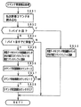
そして、払出制御用CPU371は、払出制御用のバックアップRAM領域にバックアップデータが存在しているか否かの確認を行なう(ステップS702)。すなわち、たとえば、バックアップRAM領域に形成されている後述する総合個数記憶または貸玉個数記憶(図59参照)を確認して、未払出の賞球個数および貸玉個数に関するバックアップデータがないかどうかを確認する。不測の電源断が生じた場合には、多くの場合何らかのデータがバックアップRAM領域に保存されており、バックアップRAM領域のデータは保存されていたはずであるから、後に復旧した場合の確認結果の多くはバックアップデータありとなる。バックアップなしという確認結果であれば、前回の電源オフ時に未払出の遊技球がなかったことになり、内部状態を電源断時の状態に戻す必要がないので、停電復旧時でない電源投入時に実行される初期化処理を実行する(ステップS702,S703)。なお、本例では、バックアップRAM領域にバックアップデータが存在しているか否かは、電源断時にバックアップRAM領域に設定されるバックアップフラグによって確認する。
【0249】
バックアップRAM領域にバックアップデータが存在している場合には、この実施の形態では、払出制御用CPU371は、バックアップRAM領域のデータチェック(この例ではパリティチェック)を行なう(ステップS704)。不測の電源断が生じた後に復旧した場合には、バックアップRAM領域のデータは保存されていたはずであるから、チェック結果は正常になる。チェック結果が正常でない場合には、内部状態を電源断時の状態に戻すことができないので、停電復旧時でない電源投入時に実行される初期化処理を実行する(ステップS705,S703)。
【0250】
チェック結果が正常であれば、払出制御用CPU371は、内部状態を電源断時の状態に戻すための払出状態復旧処理を行なう(ステップS706)。そして、バックアップRAM領域に保存されていたPC(プログラムカウンタ)の指すアドレスに復帰する(ステップS707)。
【0251】
通常の初期化処理の実行(ステップS703)を得ると、払出制御用CPU371により実行されるメイン処理は、タイマ割込フラグの開始(ステップS708)の確認が行なわれるグループ処理に移行する。
【0252】
なお、この実施の形態では、ステップS702でバックアップデータの有無を確認した後、バックアップデータが存在する場合にステップS704でバックアップ領域のチェックを行なうようにしていたが、逆に、バックアップ領域のチェック結果が正常であったことを確認した後、バックアップデータの有無の確認を行なうようにしてもよい。また、バックアップデータの有無の確認、または、バックアップ領域のチェックのいずれかの一方の確認を行なうことで、停電復旧処理を実行するか否かを判断するようにしてもよい。
【0253】
また、たとえば停電復旧処理を実行するか否かを判断する場合のパリティチェック(ステップS704)の際などに、すなわち、遊技状態を復旧するか否かを判断する際に、保存されていたRAMデータにおける払出遊技球数データ等によって、遊技機が払出待機状態(払出途中でない状態)であることが確認されたら、払出状態復旧処理を行なわずに初期化処理を実行するようにしてもよい。
【0254】
通常の初期化処理では、図57に示すように、レジスタおよびRAMのクリア処理(ステップS901)が行なわれる(ステップS902)。そして、初期設定処理(ステップS701a)において割込禁止とされているので、初期化処理を終える前に割込が許可される(ステップS903)。
【0255】
この実施の形態では、払出制御用CPU371の内部タイマ(CH3)が繰返しタイマ割込を発生するように設定される。また、繰返し周期は2msに設定される。そして、図58に示すように、タイマ割込が発生すると、払出制御用CPU371は、タイマ割込フラグをセットする(ステップS711)。なお、2msタイマ割込処理において、必要ならば、CH3のレジスタに対して初期値再設定が行なわれる。
【0256】
払出制御用CPU371は、ステップS708において、タイマ割込フラグがセットされことを検出すると、タイマ割込フラグをリセットするとともに(ステップS709)、払出制御処理を実行する(ステップS710)。以上の制御によって、この実施の形態では、払出制御処理は2ms毎に起動されることになる。なお、この実施の形態では、タイマ割込処理ではフラグセットのみがなされ、払出制御処理ではメイン処理において実行されるが、タイマ割込処理で払出制御処理を実行してもよい。
【0257】
払出制御用CPU371は、電源投入時に、バックアップRAM領域のデータを確認するだけで、通常の初期設定処理を行なうのか払出中の状態を復元するのかを決定できる。すなわち、簡単な判断によって、未払出の遊技球について払出処理再開を行なうことができる。
【0258】
また、本例では、払出制御用CPU371も、主基板31のCPU56と同様に、パリティチェックによって記憶内容保存の確実化を図っている。
【0259】
以上説明したように、バックアップデータの有無により電源断時の払出状態に復旧するか否かの判断を行なうようにしたことで、停電後の電源復旧時などにおいて電源投入されたときに、バックアップデータ記憶領域の内容に応じて電源断時の状態に復旧させるか否かの判断を行なうことができる。したがってバックアップデータに基づく制御を実現することができるとともに、不必要な復旧処理の実行を防止することができる。
【0260】
また、上述したように、バックアップデータの状態により電源断時の払出状態に復旧するか否かの判断を行なうようにしたことで、停電後の電源復旧時などにおいて電源投入されたときに、バックアップデータ記憶領域の内容の状態に応じて電源断時の状態に復旧させるか否かの判断を行なうことができる。したがって正常なバックアップデータに基づく制御を実現することができるとともに、異常が発生したバックアップデータに基づく復旧処理の実行を防止することができる。
【0261】
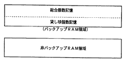
図59は、払出制御用CPU371が内蔵するRAMの使用例を示す説明図である。この例では、バックアップRAM領域に総合個数記憶(たとえば2バイト)および貸玉個数記憶が形成されている。総合個数記憶は、主基板31の側から指示された払出個数の挿通を記憶するものである。貸玉個数記憶は、未払出の球貸個数を記憶するものである。
【0262】
図60は、割込処理による払出制御コマンド受信処理を示すフローチャートである。主基板31からの払出制御用のINT信号は払出制御用CPU371のCLK/TRG2端子に入力される。よって、主基板31からのINT信号がオン状態になると、払出制御用CPU371に割込がかかり、図60に示す払出制御コマンドの受信処理が開始される。この実施の形態では、受信した払出制御コマンドを格納するための12バイトの確定コマンドバッファ領域が設けられている。 そして、受信した払出制御コマンドの格納位置を示すためにコマンド受信個数カウンタが用いられる。なお、払出コマンドは、2バイト構成であるから、実質的には6個の払出制御コマンドの確定コマンドバッファ領域に格納可能である。
【0263】
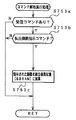
払出制御コマンドの受信処理において、払出制御用CPU371が、まず、払出制御コマンドデータの入力に割当てられている入力ポート372aからデータを読込む(ステップS851)。そして、2バイト構成の払出制御コマンドのうちの1バイト目であるか否かを確認する(ステップS852)。1バイト目であるか否かは、受信したコマンドの先頭ビットが「1」であるか否かで判断できる。先頭ビットが「1」であるのは、2バイト構成の払出制御コマンドのうちMODEバイト(1バイト目)のはずである(図50参照)。先頭ビットが「1」であれば、有効な1バイト目を保持し主として、受信したコマンドを確定コマンドバッファ領域におけるコマンド受信個数カウンタが示す確定コマンドバッファに格納する(ステップS853)。
【0264】
払出制御コマンドのうち1バイト目でなければ、1バイト目を既に受信したか否かを確認する(ステップS854)。既に受信したか否かは、受信バッファ(ステップS853における確定コマンドバッファ)に有効なデータが設定されているか否かで確認できる。
【0265】
次に、2バイト目を既に受信している場合には、受信した1バイトのうちの先頭ビットが「0」であるか否かを確認する。そして、先頭ビットが「0」であれば、有効な2バイト目を受信したとして、受信したコマンドを、確定コマンドバッファ領域におけるコマンド受信個数カウンタ+1が示す確定コマンドバッファに格納する(ステップS855)。先頭ビットが「0」であるのは、2バイト構成の払出制御コマンドのうちEXTバイト(2バイト目)のはずである(図50参照)。なお、ステップS854の判別において、受信した1バイトのうちの先頭ビットが「0」でなければ、処理を終了する。
【0266】
ステップS855において、2バイト目のコマンドデータを格納すると、コマンド受信個数カウンタに2を加算する(ステップS856)。そして、コマンド受信カウンタが12以上であるか否かを確認し(ステップS857)、12以上であればコマンド受信個数カウンタをクリアする(ステップS858)。
【0267】
図61は、ステップS710の払出制御処理を示すフローチャートである。払出制御処理において払出制御用CPU371は、まず、中継基板72を介して入力ポート372bに入力される賞球カウントスイッチ301A、球貸カウントスイッチ301Bがオンしたか否かを判定する(スイッチ:ステップS751)。
【0268】
次に、払出制御用CPU371は、センサ(たとえば、払出モータ289の間点数を検出するモータ位置センサ)からの信号入力状態を確認してセンサの状態判定などを行なう(入力判定処理:ステップS752)。払出制御用CPU371は、さらに、受信した払出制御コマンドを解析し、解析結果に応じた処理を実行する(コマンド解析実行処理:ステップS753)。
【0269】
次いで、払出制御用CPU371は、主基板31より受信した払出停止指示コマンドに応じて払出停止状態に設定し、あるいは受信した払出開始指示コマンドに応じて払出停止状態の解除を行なう(ステップS754)。また、プリペードカードユニット制御処理を行なう(ステップS755)。
【0270】
また、払出制御用CPU371は、球貸要求に応じて貸玉を払出す制御を行なう(ステップS756)。さらに、払出制御用CPU371は、総合個数記憶に格納された個数の賞球を払出す賞球制御処理を行なう(ステップS757)。そして、払出制御用CPU371は、出力ポート372cおよび中継基板72を介して玉払出装置97の払出機構部分における払出モータ289に向けて駆動信号を出力し、ステップS756の球貸制御処理またはステップS757の賞球制御処理で設定された回転数分払出モータ289を介して払出モータ制御処理を行なう(ステップS758)。
【0271】
なお、この実施の形態では、払出モータ289としてステッピングモータが用いられ、払出モータ289を制御するために1−2層励磁方式が用いられる。したがって、具体的には、払出モータ制御処理において、8種類の励磁パターンデータが繰返し払出モータ289に出力される。また、この実施の形態では、各励磁パターンデータが4msずつ出力される。
【0272】
次いで、エラー検出処理が行なわれ、その結果に応じてエラー表示LED374に所定の表示を行なう(エラー:ステップS759)。検出されるエラーとして、たとえば、次の8種類がある。
【0273】
賞球径路エラー:賞球払出動作終了したとき、または、払出モータ289が1回転したときに賞球カウントスイッチ301Aが1個も遊技球の通過を検出しなかったとき、エラー表示LED374に「0」が表示される。
【0274】
球貸径路エラー:球貸の払出動作終了後において、または、払出モータ289が1回転したときに球貸カウントスイッチ301Bが1個も遊技球の通過を検出しなかったとき、エラー表示LED374に「1」が表示される。
【0275】
賞球カウントスイッチ玉詰まりエラー:賞球カウントスイッチ301Aが0.5秒以上オンを検出したとき、エラー表示LED374に「2」が表示される。
【0276】
球貸カウントスイッチ玉詰まりエラー:球貸カウントスイッチ301Bが0.5秒以上オンを検出したとき、エラー表示LED374に「3」が表示される。
【0277】
払出モータ玉噛みエラー:払出モータ289が正常に回転しないとき。具体的には、払出モータ位置センサのオンが所定期間以上継続したり、オフが所定期間以上継続した場合、エラー表示LED374に「4」が表示される。なお、払出モータ玉噛みエラーが生じた場合には、払出制御用CPU371は、50msの基準励磁層の出力を行なった後、1−2層励磁の励磁パターンデータのうちの4種類の励磁パターンデータを8ms毎に出力することによる払出モータ289の逆回転と正回転とを繰返す。
【0278】
プリペードカードユニット未接続エラー:VL信号のオフが検出されたとき。エラー表示LED374に「5」が表示される。
【0279】
プリペードカードユニット通信エラー:規定のタイミング以外でプリペードカードユニット50から信号を出力されたことを検出したとき。エラー表示LED374に「6」が表示される。
【0280】
払出停止状態:主基板31から払出停止を示す払出制御コマンドを受信したとき。エラー表示LED374に「7」が表示される。なお、主基板31から払出開始を示す払出制御コマンドを受信したときには、その時点から2002ms後に、払出停止状態から払出開始状態に復旧する。
【0281】
外部接続端子(図示せず)から出力する情報信号を制御する処理を行なう(出力処理:ステップS760)。なお、情報信号は、貸玉の払出1単位(たとえば25個)毎に所定時間オンとなり、続いて所定時間オフを出力する信号である。
【0282】
図62は、ステップS751のスイッチ処理の一例を示すフローチャートである。スイッチ処理において、払出制御用CPU371は、賞球カウントスイッチ301Aがオンした状態を示しているか否かを確認する(ステップS751a)。オン状態を示していれば、払出制御用CPU371は、賞球カウントスイッチオンカウンタを+1する(ステップS751b)。賞球カウントスイッチオンカウンタは、賞球カウントスイッチ301Aのオンの状態を検出した回数を計数するためのカウンタである。
【0283】
そして、賞球カウントスイッチオンカウンタの値をチェックし(ステップS751c)、その値が2になっていれば、1個賞球の払出が行なわれたと判断する。1個の賞球の払出が行なわれた判断した場合には、払出制御用CPU371は、賞球未払出カウンタ(総合個数記憶に格納されている賞球数を)を−1する(ステップS751d)。
【0284】
ステップS751aにおいて賞球カウントスイッチ301Aがオン状態でないことが確認されると、払出制御用CPU371は、賞球カウントスイッチオンカウンタをクリアする(ステップS751e)。そして、この実施の形態では、球貸カウントスイッチ301Bがオン状態を示しているか否かを確認する(ステップS751f)。オン状態を示していれば、払出制御用CPU371は、球貸カウントスイッチオンカウンタを+1する(ステップS751g)。球貸カウントスイッチオンカウンタは、球貸カウントスイッチ301Bのオン状態を検出した回数を計数するためのカウンタである。
【0285】
そして、球貸カウントスイッチオンカウンタの値をチェックし(ステップS751h)、その値が2になっていれば、1個の球貸の払出が行なわれたと判断する。1個の球貸の払出が行なわれたと判断した場合には、払出制御用CPU371は、貸玉未払出個数カウンタ(貸玉個数記憶に格納されている貸玉数)を−1する(ステップS751i)。
【0286】
ステップS751fにおいて球貸カウントスイッチ301Bがオン状態でないことが確認されると、払出制御用CPU371は、球貸カウントスイッチオンカウンタをクリアする(ステップS751j)。
【0287】
図63は、ステップS753のコマンド解析実行処理の一例を示すフローチャートである。コマンド解析実行処理において、払出制御用CPU371は、確定コマンドバッファ領域中に受信コマンドがあるか否かの確認を行なう(ステップS753a)。受信コマンドがあれば、受信した払出制御コマンドが払出個数指示コマンドであるか否かの確認を行なう(ステップS753b)。なお、確定コマンドバッファ領域中に複数の受信コマンドがある場合には、受信した払出制御コマンドが払出個数指示コマンドであるか否かの確認は、最も前に受信された受信コマンドについて行なわれる。
【0288】
受信した払出制御コマンドが払出個数指示コマンドであれば、払出個数指示コマンドで受信された個数を総合個数記憶に加算する(ステップS753c)。すなわち、払出制御用CPU371は、主基板31のCPU56から送り出された払出個数指示コマンドに含まれる賞球数バックアップRAM領域(総合個数記憶)に記録する。
【0289】
なお、払出制御用CPU371は、必要ならば、コマンド受信個数カウンタの減算や確定コマンドバッファ領域における受信コマンドシフト処理を行なう。
【0290】
図64は、ステップS754の払出停止状態設定処理の一例を示すフローチャートである。払出停止状態設定処理において、払出制御用CPU371は、確定コマンドバッファ領域中に受信コマンドがあるか否かの確認を行なう(ステップS754a)。確定コマンドバッファ領域中に受信コマンドがあれば、受信した払出制御コマンドが払出停止指示コマンドであるか否かの確認を行なう(ステップS754b)。払出停止指示コマンドであれば、払出制御用CPU371は、払出停止状態に設定する(ステップS754c)。
【0291】
ステップS754bで受信コマンドが払出停止指示コマンドでないことを確認すると、受信した払出制御コマンドが払出開始指示コマンドであるか否かの確認を行なう(ステップS754d)。払出開始指示コマンドであれば、払出停止状態を解除する(ステップS754e)。
【0292】
図65は、ステップS755のプリペードカードユニット制御処理の一例を示すフローチャートである。プリペードカードユニット制御処理において、払出制御用CPU371は、カードユニット制御用マイクロコンピュータにより入力されるVL信号を検知したか否かを確認する(ステップS755a)。VL信号を検知していなければ、VL信号非検知カウンタを+1する(ステップS755b)。また、払出制御用CPU371は、VL信号非検知カウンタの値が本例では125であるか否かを確認する(ステップS755c)。VL信号非検知カウンタの値が125であれば、払出制御用CPU371は、発射制御基板91への発射制御信号出力を停止して、駆動モータ94を停止させる(ステップS755d)。
【0293】
以上の処理によって、125回(2ms×125=250ms)継続してVL信号のオフが検出されたら、玉発射禁止状態に設定される。
【0294】
ステップS755aにおいてVL信号を検知していれば、払出制御用CPU371は、VL信号非検知カウンタをクリアする(ステップS755e)。そして、払出制御用CPU371は、発射制御信号出力を停止していれば(ステップS755f)、発射制御基板91への発射制御信号出力を開始して駆動モータ94を動作可能状態にする(ステップS755g)。
【0295】
図66および図67は、ステップ756の球貸制御処理の一例を示すフローチャートである。なお、この例では、連続的な払出数の最大値を貸玉の1単位(本例では25個)としているが、他の数であってもよい。
【0296】
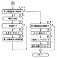
球貸制御処理において、払出制御用CPU371は、貸玉払出中であるか否かの確認を行ない(ステップS511)、貸玉払出中であれば図67に示す球貸中の処理に移行する。なお、この確認は、後述する球貸処理中フラグの状態のように判断される。貸玉払出中でなければ、賞球の払出中であるか否かの確認をする(ステップS512)。この確認は、後述する賞球処理中フラグの状態により判断される。
【0297】
貸玉払出中でも賞球払出中でもなければ、払出制御用CPU371は、カードユニット50から球貸要求があったか否かを確認し(ステップS513)、要求があれば、球貸処理中フラグをオンするとともに(ステップS514)、25(球貸1単位数:ここでは100円分)をバックアップRAM領域の貸玉個数記憶に設定する(ステップS515)。そして、払出制御用CPU371は、EXS信号をオンする(ステップS516)。そして、玉払出装置97の下方の玉振分部材311を球貸側に設定するために振分用ソレノイド310を駆動する(ステップS517)。また、払出モータ289をオンして(ステップS518)、図67に示す球貸処理に移行する。
【0298】
なお、払出モータ289がオンするのは、厳密には、カードユニット50が受付を認識したことを示すためにBRQ信号をOFFとしてからである。なお、球貸処理中フラグがバッファRAM領域に設定される。
【0299】
図67は、払出制御用CPU371による払出制御処理における球貸中の処理を示すフローチャートである。球貸処理では、払出モータ289がオンしていなければオンする。なお、この実施の形態では、ステップS751のスイッチ処理で、球貸カウントスイッチ301Bの検出出力による遊技球の払出がなされたか否かの確認を行なうため、球貸制御処理では、貸玉個数記憶の減算などは行なわれない。球貸制御処理において、払出制御用CPU371は、貸玉通過待ち時間中であるか否かの確認を行なう(ステップS519)。貸玉通過待ち時間中でなければ、貸玉の払出を行ない(ステップS520)、払出モータ289の駆動を終了すべきか(1単位の払出動作が終了したか)否かの確認を行なう(ステップS521)。具体的には、所定個数の払出に対応した回転が完了したか否かを確認する。所定個数の払出に対応した回転は、払出モータ位置センサの出力によって監視される。所定個数の払出に対応した回転が完了した場合には、払出制御用CPU371は、払出モータ289の駆動を停止し(ステップS522)、貸玉通過待ち時間の設定を行なう(ステップS523)。
【0300】
なお、ステップS520の球貸処理では、払出モータ位置センサのオンとオフとがタイマ監視されるが、所定時間以上のオン状態またはオフ状態が継続したら、払出制御用CPU371は、払出モータ玉噛みエラーが生じたと判断する。
【0301】
ステップS519で貸玉通過待ち時間中であれば、払出制御用CPU371は、貸玉通過待ち時間が終了したか否かの確認を行なう(ステップS524)。貸玉通過待ち時間は、最後の払出玉が払出モータ289によって払出されてから球貸カウントスイッチ301Bを通過するまでの時間である。貸玉通過待ち時間の終了を確認すると、1単位の貸玉はすべて払出された状態であるので、カードユニット50に対して次の球貸要求の受付が可能になったことを示すためにEXS信号をオフにする(ステップS524)。また、振分ソレノイドをオフするとともに(ステップS525)、払出モータ289をオフして(ステップS526)、さらに球貸処理中フラグをオンする(ステップS527)。なお、貸玉通過待ち時間が経過するまでに最後の払出玉が球貸カウントスイッチ301Bを通過しなかった場合には、球貸径路エラーとされる。また、この実施の形態では、賞球も球貸も同じ払出装置で行なわれる。
【0302】
なお、球貸要求の受付をEXS信号をオフした後、所定時間内に再び球貸要求信号であるBRQ信号がオンしたら、振分ソレノイドおよび払出モータをオフせずに球貸処理を実行するようにしてもよい。すなわち、所定単位(この例では100円単位)毎に球貸処理が行なわれるのではなく、球貸処理を連続して実行するように構成することもできる。
【0303】
貸玉個数記憶の内容は、遊技機の電源が断しても、所定期間電源基板910のバックアップ電源によって保存される。したがって、所定期間中に電源が回復すると、払出制御用CPU371は、貸玉個数記憶の内容に基づいて球貸処理を継続することができる。
【0304】
図68および図69は、ステップ757の賞球制御処理の一例を示すフローチャートである。なお、この例では、連続的な払出数の最大値を貸玉の1単位と同数(本例では25個)としているが、他の数であってもよい。
【0305】
賞球制御処理において、払出制御用CPU371は、貸玉払出中であるか否かの確認を行なう(ステップS531)。なお、この確認は、球貸処理中フラグの状態により判断される。貸玉払出中でなければ賞球の払出中であるか否かを確認し(ステップS532)、賞球の払出中であれば図69に示す賞球中の処理に移行する。この確認は、後述する賞球処理中フラグの状態により判断される。
【0306】
貸玉払出中でも賞球払出中でもなければ、払出制御用CPU371は、カードユニット50からの球貸準備要求があるか否かの確認を行なう(ステップS533)。なお、この確認は、払出制御用CPU371により、カードユニット50から入力されるPRDY信号のオン(要求あり)またはオフ(要求なし)を確認することにより行なわれる。
【0307】
カードユニット50からの球貸準備要求がなければ、払出制御用CPU371は、総合個数記憶に格納されている賞球数(未払出の賞球数)が0でないか否かの確認を行なう(ステップS533)。総合個数記憶に格納されている賞球数が0でなければ、賞球制御用CPU371は、賞球処理中フラグをオンし(ステップS535)、総合個数記憶の値が本例では25以上であるか否かの確認を行なう(ステップS536)。なお、賞球処理中フラグが、バックアップRAM領域に設定される。
【0308】
総合個数記憶に格納されている賞球数が25以上であると、払出制御用CPU371は、25個分の賞球を払出すまで払出モータ289を回転させるよう駆動信号出力するために、25個払出動作の設定を行なう(ステップS537)。一方、総合個数記憶に格納されている賞球数が25以上でなければ、払出制御用CPU371は、総合個数記憶に格納されているすべての遊技球を払出すまで払出モータ289を回転させるよう駆動信号出力するために、全個数払出動作の設定を行なう(ステップS538)。そして、ステップS537またはステップS538での設定に従って払出モータ289をオンする(ステップS538)。なお、振分ソレノイドはオフ状態であるため、玉払出装置97の下方の玉振分部材は賞球側に設定されている。そして、図69に示す賞球制御処理における賞球払出中の処理に移行する。
【0309】
図69は、払出制御用CPU371により払出制御処理における賞球中の処理の一例を示すフローチャートである。賞球制御処理では、払出モータ289がオンしていなければオンする。なお、この実施の形態では、ステップS751のスイッチ処理で、賞球カウントスイッチ301Aの検出出力による遊技球の払出がなされたか否かの確認を行なうため、賞球制御処理では総合個数記憶の減算などは行なわれない。賞球中の処理において、払出制御用CPU371は、賞球通過待ち時間中であるか否かの確認を行なう(ステップS540)。賞球通過待ち時間中でなければ、賞球払出を行ない(ステップS541)、払出モータ289の駆動を終了すべきか(本例では25個または25個未満の所定個数の払出動作が終了したか否かの確認を行なう(ステップS542)。具体的には、所定個数の払出に対応した回転が完了したか否かを確認する。所定個数の払出に対応した回転は、払出モータ位置センサの出力によって監視される。所定個数の払出に対応した回転が完了した場合には、払出制御用CPU371は、払出モータ289の駆動を停止し(ステップS543)、賞球通過待ち時間の設定を行なう(ステップS542)。賞球通過待ち時間は、最後の払出玉が払出モータ289によって払出されてから賞球カウントスイッチ301Aを通過するまでの時間である。
【0310】
一方、ステップS540を見て賞球通過待ち時間中であれば、払出制御用CPU371は、賞球通過待ち時間が終了したか否かの確認を行なう(ステップS544)。貸玉通過待ち時間の終了を確認すると、ステップS537またはステップS538で設定された賞球がすべて払出された状態であるので、払出モータ289をオフするとともに(ステップS544)、賞球処理中フラグをオンする(ステップS546)。なお、賞球通過待ち時間が経過するまでに最後の払出玉が賞球カウントスイッチ301Aを通過しなかった場合には、賞球径路エラーとされる。
【0311】
また、この実施の形態では、ステップS511、ステップS531の判断によって球貸が賞球処理よりも優先されることになるが、賞球処理が球貸に優先されるようにしてもよい。
【0312】
総合個数記憶および貸玉個数記憶の内容は、遊技機の電源が断しても、所定期間電源基板910のバックアップ電源によって保存される。したがって、所定期間中に電源が回復すると、払出制御用CPU371は、総合個数記憶の内容に基づいて払出処理を継続することができる。
【0313】
なお、払出制御用CPU371は、主基板31から指示された賞球個数を賞球個数記憶で総数として管理したが、賞球数毎(たとえば、15個、10個、5個)に管理してもよい。たとえば、賞球数毎に対応した個数カウンタを設け、払出個数指定コマンドを受信すると、そのコマンドで指定された個数に対応する個数カウンタを+1する。そして、個数カウンタに対応した賞球払出が行なわれると、その個数カウンタを−1する(この場合、払出制御処理にて減算処理を行なうようにする)。その場合にも、各個数カウンタはバックアップRAM領域に形成される。よって、遊技機の電源が断しても、所定期間中に電源を回復すれば、払出制御用CPU371は、各個数カウンタの内容に基づいて賞球払出処理を継続することができる。
【0314】
図70は、電源基板910の電源監視回路から電圧変化信号に基づくNMIに応じて実行される停電発生NMIの処理の一例を示すフローチャートである。なお、この実施の形態では、NMI割込番地は0066Hである。停電発生NMI処理において、払出制御用CPU371は、まず、割込禁止フラグの内容をパリティフラグに格納する(ステップS801)。次いで、割込禁止に設定する(ステップS802)。停電発生NMI処理では、本例では主基板31において実行された処理と同様に、RAM内容の保存を確実にするためのチェックサムの生成処理を行なう。その処理中に他の割込処理が行なわれたのではチェックサムの生成処理が完了しないうちの払出制御用CPU371が動作し得ない電圧にまで低下してしまうことも考えられるので、まず、他の割込が生じないような設定がなされる。なお、停電発生NMI処理におけるステップS804〜S810は、電力供給停止時の処理の一例である。
【0315】
なお、割込処理中では他の割込がかからないような仕様のCPUを用いている場合には、ステップS802の処理は不要である。
【0316】
次いで、払出制御用CPU371は、バックアップフラグが既にセットされているか否かを確認する(ステップS803)。バックアップフラグが既にセットされていれば、以後の処理を行なわない。バックアップフラグがセットされていなければ、以下の電力供給停止時処理を実行する。すなわち、ステップS804からステップS810の処理を実行する。
【0317】
まず、各レジスタの内容をバックアップRAM領域に格納する(ステップS804)。その後、バックアップフラグをセットする(ステップS805)。そして、バックアップRAM領域のバックアップチェックデータ領域に適当な初期値を設定し(ステップS806)、初期値およびバックアップRAM領域のデータについて順次排他的論理和をとった後判定し(ステップS807)、最終的な演算値をバックアップパリティデータ領域に設定する(ステップS808)。また、RAMアクセス禁止状態にする(ステップS809)。さらに、すべての出力ポートをオフ状態にする(ステップS810)。電源電圧が低下していくときには、各種信号線のレベルが不安定になってRAM内容が化ける可能性があるが、このようにRAMアクセス禁止状態にしておけば、バックアップRAM内のデータが化けることはない。
【0318】
次いで、払出制御用CPU371は、ループ処理に入る。すなわち何らの処理もしない状態になる。したがって、図54に示されたリセットIC976からのシステムリセット信号によって外部から動作禁止状態にされる前に、内部的に動作停止状態になる。よって、電源断時に確実に払出制御用CPU371は動作を停止する。その結果、上述したRAMアクセス禁止の制御および動作停止制御によって、電源電圧が低下していくことに伴って生ずる可能性がある異常動作に起因するRAMの内容破壊等を確実に防止することができる。
【0319】
なお、この実施の形態では、停電発生NMI処理では、最終部でプログラムをループ状態にしたが、ホールト(HALT)命令を発行するように構成してもよい。
【0320】
また、レジスタの内容をRAM領域に格納した後にセットされるバックアップフラグは、上述したように電源投入時において復旧すべきバックアップデータがあるか否か(停電からの復旧か否か)を判断する再に使用される。また、ステップS801からS810の処理は、払出制御用CPU371がシステムリセット回路975からのシステムリセット信号を受ける前に完了する。換言すれば、システムリセット回路975からのシステムリセット信号を受ける前に完了するように、電圧監視回路の検出電圧の設定が行なわれている。
【0321】
この実施の形態では、電力供給停止時処理開始時に、バックアップフラグの確認が行なわれる。そして、バックアップフラグが既にセットされている場合には電力供給停止時処理を実行しない。上述したように、バックアップフラグは、必要なデータのバックアップが完了し、その後電力供給停止時処理が完了したことを示すフラグである。したがって、たとえば、リセット待ちのループ状態で何らかの原因でサイドNMIが発生したとしても電力供給停止時処理が重複して実行されてしまうようなことはない。
【0322】
ただし、割込処理中では他の割込がかからないような仕様のCPUを用いている場合には、ステップS803の判断は不要である。
【0323】
また、この実施の形態では、払出制御用CPU371は、マスク不能外部割込端子(NMI端子)を介して電源基板からのNMI割込信号(電源監視手段からのNMI割込信号)を検知したが、NMI割込信号をマスク可能割込端子(IRQ端子)に導入してもよい。その場合には、IRQ処理によって、図70に示された停電発生NMI処理が実行される。また、入力ポートを介してNMI割込信号を検知してもよい。その場合には、払出制御用CPU371が実行するメイン処理において、入力ポートの監視が行なわれる。
【0324】
図71は、バックアップパリティデータ作成方法の一例を説明するための説明図である。ただし、図71に示す例では、簡単のために、バックアップデータRAM領域のデータのサイズを3バイトとする。電源電圧低下に基づく停電発生処理において、図71に示すように、バックアップチェックデータ領域に、初期データ(この例では00H)が設定される。次に、「00H」と「F0H」の排他的論理和がとられ、その結果と「16H」の排他的論理和がとられる。さらに、その結果と「DFH」の排他的論理和がとられる。そして、その結果(この例では「39H」)を反転して得られた値(この例では「C6H」)がバックアップパリティデータ領域に設定される。
【0325】
電源が再投入されたときには、停電復旧処理においてパリティ診断が行なわれる。バックアップ領域の全データがそのまま保存されていれば、電源再投入時に、図71に示すようなデータがバックアップ領域に設定されている。
【0326】
ステップS704の処理において、払出制御用CPU371は、図70のステップS806およびステップS807にて実行された処理と同様の処理を行なう。すなわち、バックアップチェックデータ領域に、初期データ(この例では00H)が設定され、「00H」と「F0H」の排他的論理和がとられ、その結果と「16H」の排他的論理和がとられる。さらに、その結果、「DFH」の排他的論理和がとられる。そして、その結果(この例では「39H」)を反転した最終演算結果を得る。バックアップ領域の全データがそのまま保存されていれば、最終的な演算結果は、「C6H」、すなわち、バックアップチェックデータ領域に設定されているデータと一致する。バックアップRAM領域内のデータにビット誤りが生じた場合には、最終的な演算結果は「C6H」にならない。
【0327】
よって、払出制御用CPU371は、最終的な演算結果とバックアップチェックデータ領域に設定されているデータとを比較して、一致すればパリティ診断正常とする。一致しなければパリティ診断異常とする。
【0328】
以上のように、この実施の形態では、払出制御手段には、遊技機の電源が断しても、所定期間電源バックアップされる記憶手段(この例ではバックアップRAM)が設けられ、電源投入時に、払出制御用CPU371(具体的には払出制御用CPU371が実行するプログラム)は、記憶手段がバックアップ状態にあればバックアップデータに基づいて払出状態を回復させる払出状態復旧処理(ステップS706)を行なうように構成される。
【0329】
以下、払出復旧処理について説明する。
図72は、図55のステップS706に示された払出状態復旧処理の一例を示すフローチャートである。この例では、払出制御用CPU371は、バックアップRAMに保存されていた値をレジスタに復元する(ステップS861)。そして、バックアップRAMに保存されていたデータに基づいて停電時の払出状態を復旧するための処理を行なう。たとえば、賞球中処理中フラグのセット等を行なう。
【0330】
払出状態を復帰させると、この実施の形態では、払出制御用CPU371は、前回の電源断時の割込許可/禁止状態を復帰させるため、バックアップRAMに保存されていたパリティフラグの値を確認する(ステップS862)。パリティフラグがクリアであれば、割込許可設定を行なう(ステップS863)。一方、パリティフラグがオンであれば、そのまま(ステップS701aで設定された割込禁止状態のまま)払出状態復旧処理を終える。
【0331】
なお、ここでは、払出状態復旧処理が終了すると払出制御メイン処理にリターンするように払出状態復旧処理プログラムが構成されているが、電力供給停止時処理において保存されているスタックポインタから出すスタックエリア(バックアップRAM領域にある)に記憶されているアドレス(電源断時のNMI割込発生時に実行されていたアドレス)に戻るようにしてもよい。
【0332】
上述したように、初期設定処理を開始した後、払出状態復旧処理を終える前まで、または、初期化処理を終える前までは、割込禁止状態とする構成としたことで、割込により処理が中断されることを防止することができるため、初期設定、バックアップデータ記憶領域の内容に応じて行なわれる電源断時の払出状態に復旧させるか否かの判断、および復旧処理(または初期化処理)を確実に完了させることができる。なお、上記のように復旧処理を終える前まで割込禁止状態とする構成とした場合であっても、電源断時の割込禁止/許可状態はパリティフラグによりバックアップしているため、復旧処理において電源断時の割込禁止/許可状態を確実に復旧させることができる。
【0333】
図73は、遊技機の電源断時の電源低下やNMI割込信号(ここでは、電源断信号)の様子を示すタイミング図である。遊技機に対する電力供給が絶たれると、最も高い直流電源電圧であるVSLの電圧値は徐々に低下する。そして、この例では、+22Vまで低下すると、電源基板910に搭載されている電源監視用CI902から電源断信号(電圧低下信号)が出力される(ローレベルになる)。
【0334】
電源断信号は、電気部品制御基板(図73に示す例では主基板31および払出制御基板37)に導入され、CPU56および払出制御用CPU371のNMI端子に入力される。CPU56および払出制御用CPU371は、上述したNNMI処理によって、所定の電力供給停止時処理を実行する。
【0335】
VSLの電圧値がさらに低下して所定値(この例では+9V)にまで低下すると、主基板31や払出制御基板37に搭載されているリセットIC651の出力がローレベルになり、CPU56および払出制御用CPU371がシステムリセット状態になる。なお、CPU56および払出制御用CPU371は、システムリセット状態とされる前に、電力供給停止時処理を完了している。
【0336】
VSLの電圧値がさらに低下してVcc(各種回路を駆動するための+5V)を生成することが可能な電圧を下回ると、各基板において各種回路が動作できない状態となる。しかし、少なくとも主基板31や払出制御基板37では、電力供給停止時処理が実行され、CPU56および払出制御用CPU371がシステムリセット状態とされている。
【0337】
リセットIC976が電源断を検知するための所定値は、CPU371を動作させる通常時の電圧より低いが、払出制御用CPU371がしばらくの間動作し得る程度の電圧である。また、リセットIC976が払出制御用CPU371が必要とする電圧(この例では+5V)よりも高い電圧を監視するように監視されているので、払出制御用CPU371が必要とする電圧に対して監視範囲を広げることができる。したがってより精密な監視を行なうことができる。
【0338】
また、この実施の形態では、電源基板910に搭載されている電源監視回路が、遊技機で使用される直流電圧のうち最も高い電源VSLの電圧を監視して、その電源の電圧が所定値を下回ったら電圧低下信号(電源断検出信号)を発生する。図73に示すように、電源断検出信号から出力されるタイミングでは、IC駆動電圧は、まだ各種回路素子を十分駆動できる電圧値になっている。したがって、IC駆動電圧で動作する払出制御基板37の払出制御用CPU371が所定の電力供給停止処理を行なうための動作時間が確保されている。
【0339】
なお、ここでも、電源監視回路は、遊技機で使用される直流電圧のうちで最も高い電源VSLの電圧を監視することになるが、電源断検出信号を発生するタイミングが、IC駆動電圧で動作する電気部品制御手段が所定の電力供給停止時処理を行なうための動作時間が確保されるようなタイミングであれば、監視対象電圧は、最も高い電源VSLの電圧でなくてもよい。すなわち、少なくともにIC駆動電圧よりも高い電圧を監視すれば、電気部品制御手段が所定の電力供給停止時処理を行なうための動作時間が確保されるようなタイミングで電源断検出信号を発生することができる。
【0340】
この場合、上述したように、監視対象電圧は、賞球カウントスイッチ301A等の遊技機の各種スイッチに供給される電圧が+12Vであることから、電源断時のスイッチオン誤検出の防止も期待できる電圧であることは好ましい。すなわち、スイッチに供給される電圧(スイッチ電圧)である+12V電源電圧が落ち始める以前の段階で、電圧低下を検出できることが望ましい。よって、少なくともスイッチ電圧よりも高い電圧を監視することが好ましい。
【0341】
ただし、監視範囲が狭まるが、電圧監視回路および他の電圧監視回路の監視電圧として+5V電源電圧を用いることも可能である。その場合にも、電圧監視回路の検出電位は、他の電圧監視回路の検出電位よりも高く設定されている。
【0342】
以上説明したようにバックアップデータの有無により電源断時の状態に復旧するか否かの判別を行なうようにしたことで、停電後の電源復旧時などにおいて電源投入されたときに、バックアップデータ記憶領域の内容に応じて電源断時のデータに復旧されるか否かの判断を行なうことができる。したがって、バックアップデータに基づく制御を実現することができるとともに、不必要な復旧処理の実行を防止することができる。
【0343】
また、上述したようにバックアップデータの状態により電源断時の状態に復旧するか否かの判断を行なうようにしたことで、停電後の電源復旧時などにおいて電源投入されたときに、バックアップデータ記憶領域の内容のデータに応じて電源断時の状態に復旧させるか否かの判断を行なうことができる。したがって、正常なバックアップデータに基づく制御を実現することができるとともに、異常が発生したバックアップデータに基づく復旧処理の実行を防止することができる。
【0344】
また、上述したように初期設定処理を開始した後、復旧処理を終える前まで、また初期処理を終える前までの値(初期準備処理の間は、)は、割込禁止状態とする構成としたことで、割込により処理が中断されることを防止することができるため、初期設定、バックアップデータ記憶領域内の内容に応じて行なわれる電源断時の状態に復旧されるか否かの判断、および復旧処理(または初期化処理)を確実に完了させることができる。なお、上記のような復旧処理を終える前まで割込禁止状態とする構成とした場合であっても、電源断時の割込禁止/許可状態をパリティフラグによりバックアップしているため、復旧処理において電源断時の割込禁止/許可状態を確実に復旧させることができる。この場合、上記初期準備処理において含まれる処理は一例であり、初期準備処理はたとえば、初期設定処理を監視した後バックアップデータに基づく復旧を行なうか否かを決定するまでの間の処理など、上述した処理の一部であってもよい。
【0345】
なお、上述した各実施の形態では、電源監視手段は、電源基板および電気部品制御基板のいずれかに設置されたが、どこに設置されていてもよく、遊技機の構造上の都合に応じて任意位置に設置することができる。
【0346】
そして、上記の各実施の形態では、記憶手段としてRAMを用いた場合を示したが、記憶手段として、電気的に書換が可能な記憶手段であればRAM以外のものを用いてもよい。
【0347】
また、上述した各実施の形態では、遊技制御手段以外の他の電気部品制御手段として払出制御手段を示したが、表示制御手段、音声制御手段およびランプ制御手段についても、上述した制御を行なうように構成してもよい。
【0348】
また、上述実施の形態では、電源監視回路は、電源基板910に設けられたが、電源監視回路は、主基板31や払出基板37の電気部品制御基板に設けられていてもよい。なお、電源回路が搭載された電気部品制御基板が構成される場合には、電源基板には、電源監視回路が搭載されない。
【0349】
上記の各実施の形態のパチンコ遊技機1は、始動入賞に基づいて可変表示部9に可変表示される特別図柄の停止図柄が所定の図柄に組合せとなると所定の遊技価値が遊技者に付与可能になる第1種パチンコ遊技機であったが、始動入賞に基づいて開放する電動役物の所定領域への入賞があると所定遊技価値が遊技者に付与可能になる第2種パチンコ遊技機や、始動入賞に基づいて可変表示される図柄の停止図柄が所定の図柄の組合せになると開放する所定電動役物への入賞があると所定の権利が発生または継続する第3種パチンコ遊技機であっても、本発明を適用できる。
【0350】
さらに、パチンコ遊技機にとらわれず、スロット遊技機等においても、電源投入による電源断時に電源断直前のデータをバックアップRAM等に保存し、電源復旧時に保存データに基づく制御再開処理を行なうように構成されている場合などには本発明を適用することができる。たとえば、スロット遊技機に適用した場合には、内部フラグ(ビッグ、レギュラー、小役などのフラグ)やビッグ中などの状態を復旧させることができる。
【0351】
上記電力監視手段は、電圧の所定の値以下になったときに信号を送り出すようにしたが、電圧が所定の値以上になったときに信号を出力するようにしてもよい。それにより、IC等の電気回路の損傷を防止できるとともに、消費電力の無駄を防止するようなことも可能となる。
【0352】
今回開示された実施の形態はすべての点で例示であって制限的なものではないと考えられるべきである。本発明の範囲は上記した説明ではなくて特許請求の範囲によって示され、特許請求の範囲と均等の意味および範囲内でのすべての変更が含まれることが意図される。
【0353】
【課題を解決する手段の具体例の効果】
請求項1に記載の本発明によれば、第2の電気部品制御基板には第1の電気部品制御基板を介して電力が供給されるため、電源基板に、電源基板と第2の電気部品制御基板と接続するためのコネクタを設ける必要がなくなる。それにより、電源基板に設けるコネクタの数を低減することができるため、電源基板の構造が簡単となる。また、電力供給停止時に確実なデータ保存が行なわれ、遊技者に不利益がもたらされることが防止される。また、第1の電源監視手段が第1の検出信号を出力するタイミングと第2の電源監視手段が第2の検出信号を出力するタイミングとの差を所望の所定時間に確実に設定することができる。さらに、チェックデータにもとづくチェックによって記憶内容保存の確実化が図られる。
また、電力供給停止時において遊技球検出手段の出力がオン状態を呈するようになる以前の段階で電力供給停止を認識して電力供給停止時処理の状態に移行するために、遊技球検出手段のオン誤検出を防止できる状態となる。さらに、第1の電気部品制御マイクロコンピュータの正常な動作が担保できない電圧にまで低下する以前の段階において、第1の電気部品制御マイクロコンピュータを動作停止状態にするために、第1の電気部品制御マイクロコンピュータが不定データに基づいて異常動作してしまう不都合を防止することができる。
【0354】
請求項2に記載の本発明によれば、請求項1に記載の発明の効果に加えて、以下のような効果がある。本発明においては、第1の電気部品制御基板が、遊技を制御するための遊技制御マイクロコンピュータを備えた遊技制御基板を含み、第2の電気部品制御基板が、遊技制御マイクロコンピュータから出力された電気信号に基づいて画像を可変表示させる可変表示手段を制御する表示制御マイクロコンピュータを備えた表示制御基板を含む。そのため、電源基板と表示制御基板とを接続するためのコネクタを電源基板に設ける必要がなくなる。それにより、機種変更にともない表示制御基板を必要としなくなる場合において、電源基板には未接続のコネクタが存在しなくなる。その結果、未接続のコネクタが存在することによって生じる、電源基板の未接続のコネクタから不正制御を行なうための情報が入力されるおそれがなくなる。したがって、機種変更にともなって生じる不正制御を予め防止するような構造にすることができる。
【0355】
請求項3に記載の本発明によれば、請求項1または請求項2に記載の発明の効果に加えて、第2の電気部品制御基板は、電気部品の制御に必要な電力を作成する電力作成手段を有しているため、外部に第2の電気部品制御基板に必要な電力を作成する電力作成手段を設ける必要がなくなる。
【0357】
請求項4に記載の本発明によれば、請求項1〜請求項3のいずれかに記載の発明の効果に加えて、電源基板が遊技の進行に応じた所定条件の成立により遊技価値を付与する制御を行なうための価値付与制御マイクロコンピュータを備えた価値付与制御基板へ必要な電力を直接供給するため、第1の電気部品制御基板は価値付与制御基板へ電力を供給するための端子等を備える必要がなくなる。その結果、第1の電気部品制御基板の構造が簡単となる。
請求項5に記載の本発明によれば、請求項1〜請求項4のいずれかに記載の発明の効果に加えて、第1の電気部品制御マイクロコンピュータにより、電力供給開始時に、電力供給停止直前の内容が記憶手段に保持されているか否かが判定されて保持されていることを条件にチェックデータにもとづくチェックが行われる一方、保持されていないときには電源投入時に実行される初期化処理が実行されるために、保持されていないときのチェックデータにもとづくチェックが省かれる。
【図面の簡単な説明】
【図1】 パチンコ遊技機の正面図である。
【図2】 パチンコ遊技機の背面図である。
【図3】 機構盤周辺の構成を示す遊技機の背面図である。
【図4】 遊技制御基板の回路構成を示すブロック図である。
【図5】 表示制御基板を回路構成を示すブロック図である。
【図6】 音声制御基板の回路構成を示すブロック図である。
【図7】 ランプ制御基板の回路構成を示すブロック図である。
【図8】 賞球制御基板に関連する構成要素を示すブロック図である。
【図9】 電源基板の周辺を示す図である。
【図10】 音声制御系統の基板を示す図である。
【図11】 音声制御基板の内部の電源引込口近傍の電気回路を示す図である。
【図12】 音声制御基板の内部のバッファ回路周辺の電気回路を示す図である。
【図13】 音声制御基板の内部の音声制御用CPU周辺の電気回路を示す図である。
【図14】 音声制御基板の内部の音声合成ICおよび音声データROMの周辺の電気回路を示す図である。
【図15】 音声制御基板の内部の音声切換回路および音声増幅回路の周辺の電気回路を示す図である。
【図16】 表示制御系統の基板を示す図である。
【図17】 表示制御基板の内部の電源引込口近傍の電気回路を示す図である。
【図18】 表示制御基板の内部のバッファ回路周辺の電気回路を示す図である。
【図19】 表示制御基板の内部の表示制御用CPU周辺の電気回路を示す図である。
【図20】 表示制御基板の内部の表示制御データROM周辺の電気回路を示す図である。
【図21】 表示制御基板の内部の水晶発振器周辺の電気回路を示す図である。
【図22】 表示制御基板の内部の水晶発振器周辺の電気回路を示す図である。
【図23】 表示制御基板の内部のリセット回路周辺の電気回路を示す図である。
【図24】 表示制御基板の内部のVDP周辺の電気回路を示す図である。
【図25】 表示制御基板の内部のVRAMおよびキャラクタROMの周辺の電気回路を示す図である。
【図26】 表示制御基板の内部のトランジスタからCRTまでの電気回路を示す図である。
【図27】 ランプ制御基板を示す図である。
【図28】 ランプ中継基板およびランプ中継A基板に接続される基板を示す図である。
【図29】 枠用ランプ中継A基板および枠用ランプ中継A基板に接続される基板を示す図である。
【図30】 ランプ制御基板の内部の電源引込口近傍の電気回路を示す図である。
【図31】 ランプ制御基板内部のバッファ回路周辺の電気回路構造を示す図である。
【図32】 ランプ制御基板内部のCPU周辺の電気回路構造を示す図である。
【図33】 ランプ制御基板からランプ中継基板へ信号を出力する配線の一部を示す図である。
【図34】 ランプ制御基板から枠用ランプ中継A基板へ信号を出力する配線の一部を示す図である。
【図35】 ランプ制御基板からランプ中継基板へ信号を出力する配線の一部を示す図である。
【図36】 ランプ制御基板からランプ中継基板へ信号を出力する配線の一部を示す図である。
【図37】 表示制御基板の他の例を示すブロック図である。
【図38】 主基板の電源入力回路周辺を示す図である。
【図39】 電源監視および電源バックアップのためのCPU周りの一構成例を示すブロック図である。
【図40】 電源基板の一構成例を示すブロック図である。
【図41】 主基板におけるCPUが実行するメイン処理の例を示すフローチャートである。
【図42】 遊技状態復旧処理を実行するか否かの決定方法の例を示す説明図である。
【図43】 初期化処理の例を示すフローチャートである。
【図44】 2msタイマ割込処理の例を示すフローチャートである。
【図45】 初期設定処理の例を示すフローチャートである。
【図46】 遊技制御処理の例を示すフローチャートである。
【図47】 停電発生NMI処理の例を示すフローチャートである。
【図48】 バックアップパリティデータ作成方法の例を説明するための説明図である。
【図49】 遊技状態復旧処理の例を示すフローチャートである。
【図50】 払出制御コマンドのコマンド形態の一例を示す説明図である。
【図51】 払出コマンドの内容の一例を示す説明図である。
【図52】 払出制御コマンドの送出形態の他の例を示すタイミング図である。
【図53】 払出制御コマンドの送出形態の一例を示すタイミング図である。
【図54】 電源監視および電源バックアップのための払出制御用CPU周りの一構成例を示すブロック図である。
【図55】 払出制御用CPUが実行するメイン処理の例を示すフローチャートである。
【図56】 払出制御用CPUの初期設定処理の一例を示すフローチャートである。
【図57】 払出制御用CPUの初期化処理の一例を示すフローチャートである。
【図58】 払出制御用CPUの初期化処理の一例を示すフローチャートである。
【図59】 払出制御手段におけるRAMの一構成例を示す説明図である。
【図60】 払出制御用CPUのコマンド受信処理の例を示すフローチャートである。
【図61】 払出制御用CPUが実行する払出制御処理の例を示すフローチャートである。
【図62】 スイッチ処理の例を示すフローチャートである。
【図63】 コマンド解析実行処理の例を示すフローチャートである。
【図64】 払出停止状態設定処理の例を示すフローチャートである。
【図65】 プリペードカードユニット制御処理の例を示すフローチャートである。
【図66】 球貸し制御処理の例を示すフローチャートである。
【図67】 球貸し制御処理の例を示すフローチャートである。
【図68】 賞球制御処理の例を示すフローチャートである。
【図69】 賞球制御処理の例を示すフローチャートである。
【図70】 払出制御用CPUが実行する停電発生NMI処理の例を示すフローチャートである。
【図71】 バックアップパリティデータ作成方法の例を説明するための説明図である
【図72】 払出制御用CPUが実行する払出復旧処理の例を示すフローチャートである。
【図73】 遊技機の電源断時の電源低下やNMI信号の様子の例を示すタイミング図である。
【符号の説明】
27 スピーカ、28b,28c 遊技効果ランプ、31 主基板、35 ランプ制御基板、37 払出制御基板、53 基本回路、56 CPU、65 システムリセット回路、70 音声制御基板、80 表示制御基板、82 CRT、91 発射制御基板、97 玉払出装置、101 表示制御用CPU、371払出制御用CPU、109 スイッチグレギュレータ、280 LCD、652 コンデンサ、902 電源監視用IC、910 電源基板、902 電源監視用IC、916 バックアップ電源となるコンデンサ、977 コンデンサ。[0001]
BACKGROUND OF THE INVENTION
The present invention relates to a gaming machine represented by a pachinko gaming machine, a coin gaming machine or a slot machine. Specifically, the present invention relates to a gaming machine in which a power supply board is provided separately from other control boards.
[0002]
[Prior art]
As an example of electrical component control means such as a pachinko game machine, a coin game machine, or a slot machine, what is conventionally known as this type of game machine, an external power source is connected to each control board. A power supply board for supplying power, a game board for controlling the gaming state of the gaming machine, a game medium payout control means for controlling the payout of game media, a display control board for controlling a variable display device whose display state can be changed, and a light emitter Some of the light emitter control means for controlling the light emission and the sound generation means include a sound control means for controlling the generation of sound.
[0003]
[Problems to be solved by the invention]
In the above gaming machine, power is separately supplied from the power supply board to each control board. For this reason, the power supply board is provided with a connector for connecting to the game board, the payout control board, the display control board, the light emitter control board, and the sound control board through wiring. As a result, it is necessary to provide a large number of connectors in the connector of the power supply board, and thus structural restrictions become severe.
[0004]
In addition, when the model is changed from the first type pachinko gaming machine having the variable display device or the third type pachinko gaming machine to the second type pachinko gaming machine not having the variable display device, the power supply board is accompanied by the model change. There is no need to replace it, but when using a power supply board provided with a connector for the display control board, the power supply board and the first or third type in the state changed to the second type pachinko gaming machine The connector for connecting the display control board used in the pachinko gaming machine remains unconnected. Therefore, when using the second type pachinko gaming machine, a wasteful connector is generated in the power supply board structure, and there is a possibility that unauthorized control information is input from the unconnected connector.
[0005]
The present invention has been made in view of the above-described problems. In the case of using a second type pachinko gaming machine, the power supply board structure is not wasted and incorrect control information is input from an unconnected connector. This is to provide a gaming machine that can prevent this.
[0006]
[Means for solving the problems and specific examples thereof]
The present invention according to
A first electric component control board (main board 31) having a first electric component control microcomputer for controlling each of the plurality of electric parts and a second electric component control having a second electric component control microcomputer A substrate (display control substrate 80);
Provided in the game area where the game balls flow down (in the center of the
Rectifying means for converting an AC voltage from an AC power source into a DC voltage (FIG. 40: the
From the DC voltage converted from the AC voltage by the rectifying means, a first DC voltage that is lower than the DC voltage and is supplied to the game ball detecting means (the voltage supplied to the various switches of the gaming machine is + 12V) and a second DC voltage (mounted on each electric component control board) which is lower than the DC voltage supplied to the game ball detecting means and is the driving power supply voltage of the first electric component control microcomputer. DC voltage generating means (FIG. 40 is a block diagram showing a configuration example of the
A DC voltage converted from an AC voltage by the rectifying means is monitored, and a first detection is made when it is detected that the DC voltage has dropped to a first detection voltage that is higher than the first DC voltage. First power supply monitoring means for outputting a signal (the first power supply monitoring circuit is a circuit for monitoring a voltage of any one of various DC currents used by the gaming machine to detect a power supply voltage drop. In the embodiment, the first power supply monitoring circuit monitors the power supply voltage of VSL, and generates a low-level voltage drop signal when the voltage value falls below a predetermined value, which is used in gaming machines. In this example, the maximum DC voltage is +30 V. In this example, the first detection condition for the first power supply monitoring means to output the detection signal is the +30 V power supply voltage. Reduced to + 22V However, the voltage value used here is an example, and other values may be used.)
The first electrical component control board is directly supplied with the first DC voltage and the second DC voltage from the power supply board (the first electrical component to which necessary power is directly supplied from the power supply means). Control means (main substrate 31)),
The second electric component control board is supplied with a DC voltage via the first electric component control board (second electric component control means supplied with electric power via the first electric component control means). (Display control board 80)),
The first electrical component control microcomputer is
The memory means (
A predetermined power supply stop process that can be executed within a predetermined period is executed by the input of the first detection signal, and a result of calculation related to the storage contents of the storage means is obtained in the power supply stop process. 47 is a flowchart showing an example of a power failure occurrence NMI process executed in response to the NMI based on the voltage change signal from the power supply monitoring circuit of the
The same DC voltage as the DC voltage monitored by the first power supply monitoring means is monitored, and the DC voltage is lower than the first detection voltage and is lower than the drive power supply voltage of the first electric component control microcomputer. Second power supply monitoring means for outputting a second detection signal when the second detection voltage is set to a higher value (the system reset
The second power supply monitoring means outputs the first power supply monitoring means after the first power supply monitoring means outputs the first detection signal and before the second power supply monitoring means outputs the second detection signal. The second detection signal is output to the first electric component control microcomputer when the electric component control microcomputer reaches the second detection voltage set so as to complete the processing when the power supply is stopped ( The reset IC 651 monitors the power supply voltage VSL that is equal to the power supply voltage monitored by the first power supply monitoring circuit, and the voltage value is a predetermined value (the power supply voltage at which the first power supply monitoring circuit outputs a voltage drop signal). Therefore, the
The first electrical component control microcomputer is stopped in response to the input of the second detection signal, performs a check based on the check data at the start of power supply, and if the check result is normal, Resuming control based on the held data held in the storage means (FIG. 41: when power to the gaming machine is turned on, in the main process, the
[0007]
According to a second aspect of the present invention, in addition to the configuration of the first aspect of the invention, the first electric component controlsubstrateIs a game control to control the gameGame control board provided with a microcomputer (first electric component control means includes game control means (main board 31) for controlling the game)The second electrical component controlsubstrateThe game controlMicrocomputerVariable display hand that variably displays images based on electrical signals output fromStepDisplay control to controlDisplay control board provided with a microcomputer (second electric component control means is a display control for controlling variable display means (variable display 10) for variably displaying an image based on an electric signal output from the game control means. Means (display control board 80).)Is included.
[0008]
According to a third aspect of the present invention, in addition to the configuration of the first or second aspect of the invention, the second electric component controlsubstrateHas electric power generation means (switching regulator 109) for generating electric power necessary for control of the electrical components.
[0010]
According to a fourth aspect of the present invention, in addition to the configuration of the invention according to any one of the first to third aspects, the power supply board gives a game value by establishing a predetermined condition according to the progress of the game. Necessary electric power is directly supplied to a value addition control board (dispensing control board 37) provided with a value addition control microcomputer for performing control.
According to a fifth aspect of the present invention, in addition to the configuration of the first aspect of the present invention, the first electric component control microcomputer is configured to stop the power supply when power supply is started. It is determined whether or not the previous contents are held in the storage means, and a check based on the check data is performed on the condition that the contents are held (after the presence or absence of the backup data is confirmed in step S2, the backup data is If it exists, the backup area is checked in step S4). If not, the initialization process executed when the power is turned on is executed (if the confirmation result indicates that there is no backup, the initialization process is executed). (Steps S2 and S3): An initialization process executed when the power is turned on is executed (Steps S5 and S3).
[0016]
[Action]
According to the first aspect of the present invention, the following effects can be obtained. Multiple electrical components operate with supplied power. FirstOne electrical component control board is provided with a first electrical component control microcomputer for controlling each of a plurality of electrical components.. FirstThe second electrical component control board is provided with a second electrical component control microcomputer for controlling each of the plurality of electrical components.. PlayBy the action of the game ball detecting means, it is detected that a prize has been won in a prize area provided in a game area where the game ball flows down, and the first electric component control is performed.substrateA detection signal is output atThe game ball detecting means outputs a high level signal when not detected and outputs a low level signal when detected.The AC voltage from the AC power source is converted into a DC voltage by the function of the rectifying means of the power supply substrate. A first DC voltage which is lower than the DC voltage and is supplied to the game ball detecting means from the DC voltage converted from the AC voltage by the rectifying means by the action of the DC voltage generating means of the power supply board, and the game A second DC voltage that is lower than the DC voltage supplied to the sphere detection means and is the drive power supply voltage of the first electric component control microcomputer is generated. By the action of the first power supply monitoring means, the DC voltage converted from the AC voltage by the rectifying means is monitored, and the DC voltage is reduced to the first detection voltage which is higher than the first DC voltage. When detected, a first detection signal is output. The first DC voltage and the second DC voltage are directly supplied from the power supply board to the first electric component control board. A DC voltage is supplied to the second electric component control board via the first electric component control board. By the action of the first electric component control microcomputer, it becomes possible to restart the control based on the held data held in the storage means capable of holding the contents immediately before the power supply is stopped when the power supply is started. , A predetermined power supply stop process that can be executed within a predetermined period by the input of the first detection signal is executed, and in the power supply stop process, a check obtained as a result of a calculation related to the storage contents of the storage means A process of saving the data in the storage means is executed. By the action of the second power supply monitoring means of the first electric component control microcomputer, the same DC voltage as the DC voltage monitored by the first power supply monitoring means is monitored, and the direct current voltage is determined from the first detection voltage. The second detection signal is output when the second detection voltage is lower than the driving power supply voltage of the first electric component control microcomputer. The second power monitoring means outputs the second detection signal after the first power monitoring means outputs the first detection signal by the action of the second power supply monitoring means of the first electric component control microcomputer. The second detection signal is output to the first electric component control microcomputer when the first electric component control microcomputer reaches the second detection voltage set so as to complete the process when the power supply is stopped Is done. The operation of the first electric component control microcomputer is stopped in response to the input of the second detection signal, and at the start of power supply, a check based on the check data is performed, and if the check result is normal, it is stored. Control is resumed based on the retained data retained in the means.
[0018]
According to the second aspect of the present invention, in addition to the action of the first aspect of the invention,,First electrical component controlOf the game control board included in the boardGame controlMicrocomputerThe game is controlled by the action of.Second electrical component controlOf the display control board included in the boardDisplay controlMicrocomputerBy the work of,Game controlMicrocomputerThe variable display means for variably displaying the image based on the electrical signal output from is controlled.
[0019]
According to the third aspect of the present invention, in addition to the function of the first or second aspect of the invention,,Second electrical component controlsubstrateThe power required for controlling the electrical components is generated by the power generation means.
[0021]
According to the fourth aspect of the present invention, in addition to the action of the invention according to any one of the first to third aspects, the game is performed by establishing a predetermined condition according to the progress of the game by the action of the power supply board. Necessary electric power is directly supplied to a value addition control board provided with a value addition control microcomputer for performing control for giving value.
According to the present invention described in
[0027]
DETAILED DESCRIPTION OF THE INVENTION
Embodiments of the present invention will be described below in detail with reference to the drawings. In the following embodiment, a pachinko gaming machine is shown as an example of a gaming machine, but the present invention is not limited thereto, and may be, for example, a coin gaming machine or a slot machine. It is possible to apply to all game machines.
[0028]
FIG. 1 is a front view of a
[0029]
A
[0030]
The
[0031]
A
[0032]
The first state of the variable winning
[0033]
A starting
[0034]
The
[0035]
The start winning ball won in the start opening 14 is detected by a start opening switch 17 (see FIG. 4) provided on the
[0036]
When the jackpot result displayed on the
[0037]
Therefore, when no restriction is placed on the continuous control of the probability variation state, the probability variation state continues indefinitely at least as long as the big hit that has reached the number of times of the probability change continues is the probability change big hit. In the case of this
[0038]
In the probability variation state, the probability of hitting the normal symbol increases, and the variable display period (variation time) from when the normal symbol variable display starts until the display result is derived and displayed is shortened. Further, in the probability variation state, the number of times the starter
[0039]
Next, the structure of the back surface of the
[0040]
The
[0041]
FIG. 3 is a rear view of the
[0042]
As shown in FIG. 3, the ball that has passed through the
[0043]
The balls paid out from the
[0044]
FIG. 4 is a block diagram for explaining a control circuit of the
[0045]
The
[0046]
The
[0047]
When a control command is output from the
[0048]
The
[0049]
The
[0050]
The
[0051]
A
[0052]
A
[0053]
The
[0054]
A
[0055]
A
[0056]
FIG. 5 is a block diagram showing a circuit configuration in the
[0057]
The
[0058]
The
[0059]
5 includes a reset circuit 83 for resetting the
[0060]
Further, in the configuration shown in FIG. 5, in the
[0061]
As an error, for example, the display control command received from the
[0062]
The
[0063]
Further, as shown in the figure, the
[0064]
FIG. 6 is a block diagram showing a signal transmission part of the voice control command in the
[0065]
In this embodiment, a voice control command for instructing voice output from the
[0066]
For example, the
[0067]
As the
[0068]
Further, a
[0069]
Further, in the configuration shown in FIG. 6, the output of the
[0070]
For example, the voice control command received from the
[0071]
The ROM (not shown) of the
[0072]
In this embodiment, the
[0073]
FIG. 7 is a block diagram showing signal transmission / reception portions in the
[0074]
The
[0075]
The lamp control command is output from output ports (output ports E and F) 575 and 576 of the I / O port unit 57 in the
[0076]
The
[0077]
As the
[0078]
Further, in the
[0079]
Further, in the configuration shown in FIG. 7, in the
[0080]
As an error, for example, the lamp control command received from the
[0081]
In FIG. 7, a
[0082]
FIG. 8 is a block diagram showing components related to the prize ball, such as components of the prize
[0083]
As shown in FIG. 8, the winning
[0084]
Detection signals from the ball
[0085]
The
[0086]
Further, a detection signal from the prize ball count switch 301 </ b> A is also input to the I / O port 57 of the
[0087]
When there is a win, a prize ball control command (prize ball number command) indicating the number of prize balls is output to the prize
[0088]
On the
[0089]
Further, the prize
[0090]
Further, the detection signal of the prize ball count switch 301A and the detection signal of the ball
[0091]
In the configuration shown in FIG. 8, the output of the
[0092]
If the winning
[0093]
The
[0094]
A ball lending switch signal and a return switch signal are given to the
[0095]
The
[0096]
Further, the
[0097]
Instead of the dispensing motor position sensor 286, by detecting the number of step pulses of the dispensing motor 289 that is a stepping motor, the dispensing operation amount (rotation amount) of the screw 288 is detected, thereby indirectly delivering the ball. May be detected. However, the use of the dispensing motor position sensor 286 that directly detects the rotation of the screw 288 has an advantage that a highly accurate detection result can be obtained. When detecting the amount of movement (rotation amount) of the screw 288 based on the number of step pulses of the stepping motor, if the control amount per step changes for some reason, an error occurs in the detected amount of operation. It is.
[0098]
By the way, when the number of balls is counted based on the output signal of the payout motor position sensor 286, the number of balls is counted based on the output signal of the count switches 301A and 301B, which output the detection signal after the ball has fallen from the screw 288. The counting operation can proceed more quickly, but there is a useless gap between the balls aligned in the screw 288, and the ball is not dispensed when the screw 288 is rotated halfway. However, there is a drawback that it is considered that one ball has been paid out. Alternatively, even if a ball is not actually paid out due to a ball biting or other cause, it is considered that one ball has been paid out.
[0099]
For this reason, the
[0100]
By performing such two-stage control, the screw 288 is rotated at a high speed until the number of balls (prize balls or rental balls) counted based on the detection output of the payout motor position sensor 286 reaches the payout planned number. The balls can be dispensed quickly by paying out the balls continuously, and even if there is a shortage of dispensing, it is possible to accurately dispense the balls by paying out the shortage later. can do.
[0101]
From the winning
[0102]
Further, a card balance display signal indicating a balance of the prepaid card and a ball lending possible display signal are given to the
[0103]
When the power of the
[0104]
As described above, all signals from the
[0105]
In this embodiment, in addition to the RAM 55 (see FIG. 4) of the
[0106]
Here, the connection between each board | substrate of the above
[0107]
First, the
[0108]
In addition, as shown in FIG. 10, the
[0109]
Next, the electrical circuit structure inside the
[0110]
As described above, the voltage AVcc used in the voice synthesis IC for processing the analog signal is generated in the
[0111]
Also, as shown in FIG. 12, the wiring C connected from the
[0112]
Next, as shown in FIG. 14, the SICK signal, the SI signal, the SIRQ signal, the SRDY signal, and the PRES signal are respectively sent to the
[0113]
Next, as shown in FIG. 15, the DAOL signal and the DAOR signal pass through the
[0114]
According to the present embodiment as described above, since the electric signal information is transmitted only from the
[0115]
Since the
[0116]
The power of the voltage Vcc (+ 5V) supplied from the
[0117]
Next, an electric circuit structure related to the
[0118]
Next, the electrical circuit structure inside the
[0119]
As described above, the voltage AVDD used in a circuit for processing an analog signal such as the
[0120]
Also, as shown in FIG. 18, the
[0121]
Next, as shown in FIG. 19, the IN0 to IN7 signals and the INT signal are input to the
[0122]
According to the present embodiment as described above, since the
[0123]
In addition, since the
[0124]
The power of the voltage Vcc (5V) supplied from the
[0125]
Next, the structure of the electric circuit related to the
[0126]
As shown in FIG. 28, the lamp
[0127]
As shown in FIG. 29, the lamp
[0128]
Next, the internal structure of the
[0129]
Further, as shown in FIG. 31, the
[0130]
Next, as shown in FIG. 32, each of the LCD0 signal to the LCD7 signal is input to the
[0131]
Next, as shown in FIG. 33, each of the FLANP (A) signal, the FLANP (B) signal, the FLANP (C) signal, the TLANP signal, the FLANP (D) signal, the SLARP signal, and the FLANP (E) signal are Are input to
[0132]
Thereafter, the signal output from the
[0133]
Further, as shown in FIG. 34, the FLED (A) signal, the FLED (B) signal, the FLED (C) signal, and the FLED (D) signal each include an inverter circuit including a transistor provided in a manner for preventing a backflow of current. 521, 522, 523, 524, 525, 526, 527, 528, wiring 11/18, 12/18, 13/18, 14/18, 15/18, 16/18, 17/18, 18 / In order to control the left speaker outside LED, the left speaker LED, the right speaker LED, and the right speaker outside LED corresponding to the
[0134]
Further, as shown in FIG. 35, the BLED (A) signal, the BLED (B) signal, the BLED (C) signal, the BLED (D) signal, the BLED (E) signal, and the BLED (F) signal are respectively reverse currents.
[0135]
Further, as shown in FIG. 36, the MMRY (a) signal, the MMRY (b) signal, the MMRY (c) signal, and the MMRY (d) signal each include an inverter circuit including a transistor provided in a manner to prevent a reverse current flow. In order to control LED1, LED2, LED3, and LED4 corresponding to the
[0136]
The power of voltage VSL (30V) supplied from the
[0137]
The
[0138]
According to the
[0139]
In the block diagram of FIG. 5, the embodiment in which the
[0140]
FIG. 38 shows a power input circuit immediately after the
[0141]
In the
[0142]
According to the pachinko gaming machine of the present embodiment as described above, since power is supplied from the
[0143]
Further, according to the pachinko gaming machine of the present embodiment, it is not necessary to provide a connector for connecting the
[0144]
Further, according to the pachinko gaming machine of the present embodiment, each of the
[0145]
FIG. 39 is a block diagram showing a configuration example around the
[0146]
FIG. 39 also shows a
[0147]
As shown in FIG. 39, the reset signal from the reset IC 651 is input to the NAND circuit 947 (logical product circuit) and also input to the clear terminal of the
[0148]
For example, the detection voltage of the first power supply monitoring circuit (the voltage that outputs the voltage drop signal) is set to + 22V, and the detection voltage of the second power supply monitoring circuit is set to + 9V. In such a configuration, since the first power supply monitoring circuit and the second power supply monitoring circuit monitor the voltage VSL of the same power supply, the timing at which the first power supply monitoring circuit outputs the voltage drop signal. And the timing at which the second voltage monitoring circuit outputs the voltage drop signal can be reliably set to a desired predetermined time. The desired predetermined time is a period from when the power supply stop process is started in response to the voltage drop signal generated from the first power supply monitoring circuit until the power supply stop process is reliably completed.
[0149]
In this example, the first detection condition for the first power supply monitoring means to output the detection signal is that the + 30V power supply voltage has dropped to + 22V, and the second power supply monitoring means outputs the detection signal. The second detection condition is that the + 30V power supply voltage has dropped to + 9V. However, the voltage value used here is an example, and other values may be used.
[0150]
However, although the monitoring range is narrowed, it is also possible to use a + 5V power supply voltage as the monitoring voltage of the first voltage monitoring circuit and the second voltage monitoring circuit. Also in that case, the detection voltage of the first voltage monitoring circuit is set higher than the detection voltage of the second voltage monitoring circuit.
[0151]
While power is not being supplied from the + 5V power source that is the driving power source of the
[0152]
Note that FIG. 39 shows a configuration in which the reset signal (low level signal) is given to the reset terminal of the
[0153]
The delay time defined by the capacity of the
[0154]
Further, in addition to the
[0155]
The system reset
[0156]
FIG. 40 is a block diagram illustrating a configuration example of the
[0157]
The transformer 911 converts AC voltage from the AC power source into 24V. The AC 24V voltage is output to the
[0158]
The + 5V line from the DC-DC converter 913 branches to form a backup + 5V line. A large-
[0159]
A battery that can be charged from a + 5V power supply may be used as the backup power supply. In the case of using a battery, a rechargeable battery is used in which the capacity disappears when a state in which no power is supplied from the +5 V power source continues for a predetermined time.
[0160]
The
[0161]
The predetermined value for the
[0162]
Further, since the
[0163]
In the configuration shown in FIG. 40, the detection output (voltage drop signal) of the
[0164]
Next, the operation of the gaming machine will be described.
FIG. 41 is a flowchart showing main processing executed by the
[0165]
Then, it is confirmed whether or not the data width of the backup RAM area has been processed (in this example, NMI processing for generating a power failure such as a parity data load) when the power is turned off (step S2). When an unexpected power interruption occurs, processing for protecting data in the backup RAM area is performed as will be described later. When such protection processing is performed, it is assumed that there is a backup. If the confirmation result indicates that there is no backup, initial processing is executed (steps S2 and S3). In this example, whether or not there is backup data in the backup RAM area is confirmed by the state of the backup flag set in the backup RAM area when the power is turned off. In this example, if “55H” is set in the backup flag area, it means that there is a backup (ON state), and if a value other than “55H” is set, it means that there is no backup (OFF state).
[0166]
If there is backup data in the backup RAM area, in this embodiment, the
[0167]
If the check result is normal, the
[0168]
When the normal initialization process (steps S2 and S3) is finished, the main process executed by the
[0169]
In this embodiment, after the presence or absence of backup data is confirmed in step S2, the backup area is checked in step S4 if backup data exists. Conversely, the backup area check result After confirming that the data is normal, the presence or absence of backup data may be confirmed. Further, it may be configured to determine whether or not to execute the power failure recovery processing by confirming either one of the presence / absence of backup data or the confirmation of the backup area.
[0170]
In the normal initialization process, as shown in FIG. 43, a RAM clear process is performed (step S3a). Next, based on the address value of the work area initial setting table, it is initialized to a predetermined work area (for example, a normal symbol determination random number counter, a normal symbol determination buffer, a special symbol left middle right symbol buffer, a payout command storage pointer, etc.) Initial value setting processing (step S3b) for setting a value is performed. Then, initialization of a timer register provided in the CPU 56 (setting that the timeout is 2 ms and the repeated timer operates) is performed so that a timer interrupt is periodically generated every 2 ms (step S3c). That is, in step S3c, a process for activating a timer interrupt and a process for setting a timer interrupt interval are executed. Since the interruption is prohibited (see FIG. 45) in the initial setting process (step S1), the interruption is permitted before the initialization process is finished (step S3d).
[0171]
Therefore, in this embodiment, the internal timer of the
[0172]
When detecting that the timer interrupt flag is set in step S9, the
[0173]
As described above, the backup data storage area when the power is turned on at the time of power restoration after a power failure, etc., by determining whether or not to restore to the power-off state depending on the presence or absence of backup data It is possible to determine whether or not to restore the power-off state according to the contents of. Therefore, it is possible to realize control based on the backup data and to prevent unnecessary recovery processing from being executed.
[0174]
In addition, by determining whether or not to restore to the power-off state depending on the status of the backup data, the contents of the backup data storage area will be stored when the power is turned on when the power is restored after a power failure. It is possible to determine whether or not the state is restored to the state at the time of power-off according to the state. Therefore, it is possible to realize control based on normal backup data and to prevent execution of recovery processing based on backup data in which an abnormality has occurred.
[0175]
FIG. 45 is a flowchart showing the initial setting process of step S1. In the initial setting process, the
[0176]
Note that there are the following three types of maskable interrupt modes that are allowed to be interrupted by the input of an INT signal that can be set in the initial setting process.
[0177]
Interrupt mode 0: This mode is set at reset, and the address (00 (H) to 38 (H)) specified from the interrupt source by the RST instruction which is a 1-byte CALL instruction is an interrupt processing program. This is a mode indicating the start address.
[0178]
Interrupt mode 1: This is a mode in which the start address (38 (H)) of the interrupt processing program is predetermined.
[0179]
Interrupt mode 2: The address constituted by the value of the specific register (1 byte) of the
[0180]
FIG. 46 is a flowchart showing the game control process of step S11. In the game control process, the
[0181]
Subsequently, abnormality diagnosis processing is performed by a self-diagnosis function provided in the
[0182]
Next, a process of updating each counter indicating each determination random number such as a big hit determination random number used for game control is performed (step S23). The
[0183]
Further, the
[0184]
Further, the
[0185]
Next, the
[0186]
[0187]
As described above, the main process includes a process for determining whether or not to shift to the game control process, and the game control process is a timer interrupt process based on a timer interrupt periodically generated by the internal timer of the
[0188]
Conventional general game control processing is forcibly returned to the initial state by an external interrupt that occurs periodically. If it demonstrates in accordance with the example shown by FIG. 46, for example, even if it was during the process of step S31, it was forcibly returned to the process of step S21. That is, there is a possibility that the next game control process may be started before all the processes in the game control process have completed execution.
[0189]
Here, the game control process executed by the
[0190]
Even in such a configuration, the determination of the flag is not performed until all of the game control processes are executed, so that it is guaranteed that all the processes in the game control processes are completed. .
[0191]
FIG. 47 is a flowchart showing an example of a power failure occurrence NMI process executed in response to the NMI based on the voltage change signal from the power supply monitoring circuit of the
[0192]
Further, when a CPU that is used so that no other interrupts are generated during the interrupt process, the process of step S42 is not necessary.
[0193]
Next, the
[0194]
First, the contents of each register are stored in the backup RAM area (step S44). Thereafter, a backup flag is set (step S45). Then, an appropriate initial value is set in the backup check data area of the backup RAM area (step S46), the initial value and the data in the backup RAM area are sequentially subjected to exclusive OR, and then inverted (step S47). The calculated value is set in the backup parity data area (step S48). Further, the RAM access is prohibited (step S49). Further, all output ports are turned off (step S50). When the power supply voltage is lowered, the level of various signal lines may become unstable and the contents of the RAM may be changed. If the RAM access is prohibited as described above, the data in the backup RAM may be changed. There is no.
[0195]
Subsequently, the
[0196]
In this embodiment, in the power failure occurrence NMI processing, the program is looped at the final part, but a halt (HALT) instruction may be issued.
[0197]
Further, as described above, the backup flag that is set after the register contents are stored in the RAM area determines whether or not there is backup data to be restored when the power is turned on (whether or not it is restored from a power failure). Used when. Further, the processing of steps S41 to S50 is completed before the
[0198]
In this embodiment, the backup flag is confirmed at the start of the power supply stop process. If the backup flag is already set, the power supply stop process is not executed. As described above, the backup flag is a flag indicating that the backup of necessary data has been completed and the power supply stop process has been completed thereafter. Therefore, for example, even if NMI occurs again for some reason in a loop waiting for resetting, the power supply stop process is not repeatedly executed.
[0199]
However, if a CPU with a specification that does not allow other interrupts during interrupt processing is used, the determination in step S43 is not necessary.
[0200]
FIG. 48 is an explanatory diagram for explaining an example of a backup parity data creation method. However, in the example shown in FIG. 48, the data size of the backup data RAM area is 3 bytes for simplicity. In the power failure generation process based on the power supply voltage drop, as shown in FIG. 48, initial data (00H in this example) is set in the backup check data area. Next, an exclusive OR of “00H” and “F0H” is taken, and an exclusive OR of “16H” is obtained with the result. As a result, an exclusive OR of “DFH” is taken. Then, a value (“C6H” in this example) obtained by inverting the result (“39H” in this example) is set in the backup parity data area.
[0201]
When the power is turned on again, a parity diagnosis is performed in the power failure recovery process. If all the data in the backup area is stored as it is, data as shown in FIG. 48 is set in the backup area when the power is turned on again.
[0202]
In the process of step S4, the
[0203]
Therefore, the
[0204]
As described above, in this embodiment, the game control means is provided with a storage means (in this example, a backup RAM) that is backed up for a predetermined period even when the power of the gaming machine is cut off. The CPU 56 (specifically, a program executed by the CPU 56) is configured to perform a game state recovery process (step S6) for recovering the game state based on the backup data if the storage means is in the backup state.
[0205]
In this embodiment, a power supply monitoring circuit is mounted on the
[0206]
Then, the
[0207]
Thus, in this embodiment, the
[0208]
In this embodiment, the
[0209]
In the above embodiment, the
[0210]
Further, when an interrupt signal from the
[0211]
In this embodiment, in the power failure occurrence process (power supply stop process), when the backup flag indicating that the data has already been backed up and the power supply stop process has already been executed is set up, The supply stop process is not executed. In the process of powering down, NMI may occur again. Then, when the backup flag is not confirmed in the power generation process, the power supply stop process is executed again by the NMI that is generated again. In the power supply stop process executed first, a process of storing the contents of the register in the backup RAM is performed (see step S44 in FIG. 46). In a state of waiting for reset after the first process of stopping the normal power supply that is executed first, the power supply voltage gradually decreases, so that the contents of the register may be destroyed. That is, there is a possibility that the register value has changed from the state at the time when the power interruption is detected (when NMI first occurs). If the power supply stop process is executed again in such a state, a value different from the register value in the state when the power supply is detected is stored in the backup RAM. Then, in the power recovery process executed at the time of power recovery, a value different from the register value in the state at the time when the power interruption is detected is restored to the register. As a result, there is a possibility that a gaming state different from the gaming state when the power is turned off is reproduced.
[0212]
Hereinafter, the gaming state restoration process will be described.
FIG. 49 is a flowchart showing an example of the gaming state recovery process shown in step S6 of FIG. In this example, the
[0213]
As described above, in the game state restoration process, the state of various electrical components is restored according to the restored internal state, and the
[0214]
As a result, in this embodiment, the following state recovery is possible by the game state recovery process. The states of the
[0215]
When the power is cut off during the change of the special symbol, the information of the change time (for example, 10 seconds) of the variable display pattern and the already executed time (for example, 4 seconds) is backed up. Then, the
[0216]
Even if the power is cut off during the big hit game, the remaining time of the interval during the round or between rounds is displayed at the time of recovery, as in the case of the power off during the special symbol change described above. The
[0217]
As a result, it is possible to produce a jackpot symbol during a round or between rounds (for models that produce a jackpot symbol with a jackpot symbol), and the
[0218]
The display states of the
[0219]
The sound generation state controlled by the sound control means is restored except when the special symbol is changing and the big hit game is being played. However, if the game is a big hit game when the power is turned off, it can be restored to the initial state of each control section. When the power is cut off during the special symbol fluctuation, the sound generation state is controlled for the remaining time as in the display control of the
[0220]
In this embodiment, the control command for restoring the state is sent from the game control means of the
[0221]
Further, as will be described later, since the payout control means mounted on the
[0222]
When the gaming state is restored to the power-off state, in this embodiment, the
[0223]
Here, the gaming state restoration processing program is configured to return to the main processing when the gaming state restoration processing ends, but the stack area (backup RAM) pointed to by the stack pointer stored in the power supply stop processing It is also possible to return to the address stored in the area) (the address that was executed when the NMI interrupt occurred when the power was turned off).
[0224]
As described above, the process is interrupted due to the interrupt disabled state between the start of the initial setting process and before the restoration process or before the initialization process is completed. Therefore, the initial setting, determination of whether or not to restore the power-off state according to the contents of the backup data storage area, and recovery processing (or initialization processing) are ensured. Can be completed. Even in the case of the configuration in which the interrupt is disabled until the completion of the recovery processing as described above, the interrupt disabled / permitted state at the time of power-off is backed up by the parity flag. The interrupt disabled / permitted state when the power is turned off can be reliably recovered.
[0225]
In the above embodiment, the case where the data storage process and the restoration process are performed in the game control means has been described. However, part of the RAM in the payout control means, the voice control means, the lamp control means, and the display control means is also included. The power supply is backed up, and the payout control means, the display control means, the sound control means, and the lamp control means may perform the processing as described above. However, the payout control means, the display control means, the sound control means, and the lamp control means do not need to perform command transmission processing at the time of recovery.
[0226]
FIG. 50 is an explanatory diagram showing an example of a command form of the payout control command. In this embodiment, the payout control command has a 2-byte structure, the first byte represents MODE (command classification), and the second byte represents EXT (command type). Note that the command form shown in FIG. 50 is an example, and other command forms may be used.
[0227]
FIG. 51 is an explanatory diagram showing an example of the contents of the payout control command. In the example shown in FIG. 51, the command FF00 (H) is a payout control command for designating a payout enabled state. Command FF01 (H) is a payout control command for designating a payout stop state. Command F0XX (H) is a payout control command for designating the number of winning balls. “XX” in the second byte indicates the number of payouts.
[0228]
When the payout control means receives the FF01 (H) payout control command from the game control means of the
[0229]
FIG. 52 is a timing chart showing an example of a payout control command sending form. In this embodiment, the payout control command has a 2-byte structure. For example, as shown in FIG. 52, when the first byte and the second byte of the payout control signal are output, the INT signal is turned on. (Low level in this example). The ON period of the INT signal is, for example, 1 μs or longer, and a period of, for example, 10 μs or longer is provided between the first byte and the second byte. The payout control command may have a 1-byte configuration.
[0230]
The payout control command is sent out only once so that the payout control means can recognize it. In this example, “recognizable” means that the INT signal is turned on, and in this example, it is sent out only once in a recognizable manner, depending on the first and second bytes of the payout control signal. That is, the INT signal is turned on only once.
[0231]
As shown in FIG. 53, the payout control command may have a 1-byte configuration. In this case, a payout control command is output by the 8-bit payout control signals CD0 to CD7. When the payout control signal is output, the INT signal is turned on (low level in this example). The ON period of the INT signal is 1 μs or more, for example. The payout control means inputs payout control signals CD0 to CD7 by an interrupt process according to the INT signal.
[0232]
Next, as an example of the case where the data storage process and the recovery process are performed in the electrical component control means other than the game control means, a case where the payout control means performs the data storage and recovery will be described.
[0233]
FIG. 54 is a block diagram showing an example of the configuration around the
[0234]
The INT signal from the
[0235]
Although a system
[0236]
The predetermined value for the
[0237]
While power is not supplied from the power supply of voltage + 5V, at least a part of the built-in RAM of the
[0238]
As described above, in this embodiment, the first power supply monitoring circuit mounted on the
[0239]
Also in this case, the first power supply monitoring circuit monitors the highest power supply voltage VSL among the DC voltages used in the gaming machine. The monitoring target voltage may not be the highest power supply voltage VSL as long as the operation time for the electric component control means operating at the voltage to ensure the predetermined power supply stop processing is ensured. That is, when a voltage higher than at least the IC drive voltage is sensed, the power-off detection signal may be generated at such a timing that the operation time for the electrical component control means to perform a predetermined power supply stop process is secured. it can.
[0240]
In this case, as described above, the voltage to be monitored is a voltage that can be expected to prevent erroneous switch-on detection when the power is cut off because the voltage supplied to various switches of the gaming machine such as the prize ball count switch 301A is + 12V. It is preferable. That is, it is preferable to detect a voltage drop at a stage before the +12 V power supply voltage, which is a voltage supplied to the switch (switch voltage) starts to drop. Therefore, it is desirable to monitor a voltage higher than at least the switch voltage.
[0241]
In the configuration shown in FIG. 54, the system reset
[0242]
The delay time defined by the capacity of the
[0243]
Further, in addition to the
[0244]
The system reset
[0245]
FIG. 55 is a flowchart showing main processing of the
[0246]
FIG. 56 is a flowchart showing the initial setting process in step S701. In the initial setting process, the
[0247]
In this embodiment, an interrupt based on counting up of CH2 and CH3 is used as a timer / counter interrupt. The interrupt based on the count-up of CH2 is an interrupt that occurs when the value of the timer counter register CLK / TRG2 described above becomes “0”. Accordingly, in step S701e, the initial value “1” is set in the timer counter register CLK / TRG2. The interrupt based on the count up of CH3 is an interrupt that occurs after the CPU internal clock is counted down and the register value becomes “0”, and is used as a 2 ms timer interrupt described later. Specifically, the register value of CH3 is subtracted at 1/256 period of the system clock. In step S701e, the CH3 register is set to a value corresponding to 2 ms as an initial value. The interrupt address related to CH2 is 0074H, and the interrupt address related to CH3 is 0076H.
[0248]
Then, the
[0249]
When backup data exists in the backup RAM area, in this embodiment, the
[0250]
If the check result is normal, the
[0251]
When the normal initialization process is executed (step S703), the main process executed by the
[0252]
In this embodiment, after the presence or absence of backup data is confirmed in step S702, the backup area is checked in step S704 when backup data exists. Conversely, the check result of the backup area After confirming that the data is normal, the presence or absence of backup data may be confirmed. Further, it may be determined whether or not to execute the power failure recovery process by confirming one of the confirmation of the presence / absence of backup data and the check of the backup area.
[0253]
Further, for example, in the parity check (step S704) when determining whether or not to execute the power failure recovery processing, that is, when determining whether or not to restore the gaming state, the stored RAM data If the game machine is confirmed to be in a payout standby state (a state that is not in the middle of payout) based on the payout game ball number data or the like, the initialization process may be executed without performing the payout state recovery process.
[0254]
In the normal initialization process, as shown in FIG. 57, a register and RAM clear process (step S901) is performed (step S902). Since the interruption is prohibited in the initial setting process (step S701a), the interruption is permitted before the initialization process is completed (step S903).
[0255]
In this embodiment, the internal timer (CH3) of the
[0256]
When detecting that the timer interrupt flag is set in step S708, the
[0257]
The
[0258]
In this example, the
[0259]
As described above, the backup data is restored when the power is turned on when the power is restored after a power failure, etc. It is possible to determine whether or not to restore the power-off state according to the contents of the storage area. Therefore, control based on the backup data can be realized, and unnecessary execution of recovery processing can be prevented.
[0260]
In addition, as described above, by determining whether or not to return to the payout state when the power is cut off according to the backup data status, the backup is performed when the power is turned on when the power is restored after a power failure. It can be determined whether or not to restore the power-off state according to the state of the contents of the data storage area. Therefore, it is possible to realize control based on normal backup data and to prevent execution of recovery processing based on backup data in which an abnormality has occurred.
[0261]
FIG. 59 is an explanatory diagram showing an example of use of the RAM built in the
[0262]
FIG. 60 is a flowchart showing a payout control command reception process by an interrupt process. The payout control INT signal from the
[0263]
In the payout control command reception process, the
[0264]
If it is not the first byte of the payout control command, it is confirmed whether or not the first byte has already been received (step S854). Whether it has already been received can be confirmed by checking whether valid data is set in the reception buffer (the definite command buffer in step S853).
[0265]
Next, when the second byte has already been received, it is confirmed whether or not the first bit of the received 1 byte is “0”. If the first bit is “0”, it is determined that the valid second byte has been received, and the received command is stored in the confirmed command buffer indicated by the command reception number counter + 1 in the confirmed command buffer area (step S855). The leading bit is “0”, which should be the EXT byte (second byte) of the 2-byte payout control command (see FIG. 50). If it is determined in step S854 that the first bit of the received 1 byte is not “0”, the process ends.
[0266]
When the second byte of command data is stored in step S855, 2 is added to the command reception number counter (step S856). Then, it is confirmed whether or not the command reception counter is 12 or more (step S857). If it is 12 or more, the command reception number counter is cleared (step S858).
[0267]
FIG. 61 is a flowchart showing the payout control process in step S710. In the payout control process, the
[0268]
Next, the
[0269]
Next, the
[0270]
Further, the
[0271]
In this embodiment, a stepping motor is used as the payout motor 289, and a 1-2 layer excitation method is used to control the payout motor 289. Therefore, specifically, eight types of excitation pattern data are repeatedly output to the payout motor 289 in the payout motor control process. In this embodiment, each excitation pattern data is output by 4 ms.
[0272]
Next, error detection processing is performed, and predetermined display is performed on the
[0273]
Prize ball path error: When the prize ball payout operation is completed, or when no prize ball count switch 301A detects the passing of a game ball when the payout motor 289 makes one rotation, the
[0274]
Ball lending path error: After the ball lending payout operation is completed, or when the ball lending
[0275]
Prize ball count switch clogging error: When prize ball count switch 301A detects ON for 0.5 seconds or more, “2” is displayed on
[0276]
Ball lending count switch clogging error: When the ball lending
[0277]
Discharge motor ball biting error: When the discharge motor 289 does not rotate normally. Specifically, “4” is displayed on the
[0278]
Prepaid card unit unconnected error: When VL signal OFF is detected. “5” is displayed on the
[0279]
Prepaid card unit communication error: When it is detected that a signal is output from the
[0280]
Discharge stop state: When a payout control command indicating a payout stop is received from the
[0281]
Processing for controlling an information signal output from an external connection terminal (not shown) is performed (output processing: step S760). Note that the information signal is a signal that is turned on for a predetermined time every 1 unit (for example, 25) of paying out a ball and subsequently outputs OFF for a predetermined time.
[0282]
FIG. 62 is a flowchart illustrating an example of the switch process in step S751. In the switch process, the
[0283]
Then, the value of the prize ball count switch-on counter is checked (step S751c). If the value is 2, it is determined that one prize ball has been paid out. If it is determined that one prize ball has been paid out, the
[0284]
When it is confirmed in step S751a that the prize ball count switch 301A is not in the on state, the
[0285]
Then, the value of the ball lending count switch-on counter is checked (step S751h). If the value is 2, it is determined that one ball lending has been paid out. If it is determined that one ball lending has been paid out, the
[0286]
When it is confirmed in step S751f that the ball lending
[0287]
FIG. 63 is a flowchart illustrating an example of the command analysis execution process in step S753. In the command analysis execution process, the
[0288]
If the received payout control command is a payout number instruction command, the number received by the payout number instruction command is added to the total number memory (step S753c). That is, the
[0289]
The
[0290]
FIG. 64 is a flowchart showing an example of the payout stop state setting process in step S754. In the payout stop state setting process, the
[0291]
If it is confirmed in step S754b that the received command is not a payout stop instruction command, it is checked whether or not the received payout control command is a payout start instruction command (step S754d). If it is a payout start instruction command, the payout stop state is canceled (step S754e).
[0292]
FIG. 65 is a flowchart showing an example of the prepaid card unit control process in step S755. In the prepaid card unit control process, the
[0293]
If the VL signal is detected to be off 125 times (2 ms × 125 = 250 ms) continuously by the above processing, the ball firing prohibited state is set.
[0294]
If the VL signal is detected in step S755a, the
[0295]
66 and 67 are flowcharts showing an example of the ball lending control process in
[0296]
In the ball lending control process, the
[0297]
If the ball lending is not being paid out or the winning ball is not being paid out, the
[0298]
Strictly speaking, the payout motor 289 is turned on after the BRQ signal is turned off to indicate that the
[0299]
FIG. 67 is a flowchart showing a ball lending process in the payout control process by the
[0300]
In the ball lending process in step S520, the on / off state of the payout motor position sensor is monitored by a timer, but if the on state or the off state continues for a predetermined time or longer, the
[0301]
If it is during the ball lending passage waiting time in step S519, the
[0302]
After turning off the EXS signal to accept the ball rental request, if the BRQ signal, which is the ball rental request signal, is turned on again within a predetermined time, the ball rental process is executed without turning off the sorting solenoid and the dispensing motor. It may be. That is, the ball lending process is not performed every predetermined unit (100 yen unit in this example), but the ball lending process can be executed continuously.
[0303]
The contents of the number of rented balls are stored by the backup power supply of the
[0304]
68 and 69 are flowcharts showing an example of the prize ball control process in
[0305]
In the winning ball control process, the
[0306]
If neither the ball rental is paid out nor the prize ball is paid out, the
[0307]
If there is no ball lending preparation request from the
[0308]
If the number of prize balls stored in the total number memory is 25 or more, the
[0309]
FIG. 69 is a flowchart illustrating an example of a process during a prize ball in the payout control process by the
[0310]
On the other hand, if it is during the winning ball passage waiting time as seen in step S540, the
[0311]
Further, in this embodiment, the ball rental is prioritized over the prize ball processing according to the determinations in steps S511 and S531, but the prize ball processing may be prioritized over the ball rental.
[0312]
The contents of the total number storage and the rented number storage are stored by the backup power source of the
[0313]
The
[0314]
FIG. 70 is a flowchart illustrating an example of a power failure occurrence NMI process executed in response to the NMI based on the voltage change signal from the power supply monitoring circuit of the
[0315]
Note that the processing in step S802 is not necessary when a CPU having a specification that does not cause other interrupts during the interrupt processing is used.
[0316]
Next, the
[0317]
First, the contents of each register are stored in the backup RAM area (step S804). Thereafter, a backup flag is set (step S805). Then, an appropriate initial value is set in the backup check data area of the backup RAM area (step S806), and after the exclusive OR is sequentially obtained for the initial value and the data in the backup RAM area, the determination is made (step S807). The calculated value is set in the backup parity data area (step S808). In addition, the RAM access is prohibited (step S809). Further, all output ports are turned off (step S810). When the power supply voltage is lowered, the level of various signal lines may become unstable and the contents of the RAM may be altered, but if the RAM access is prohibited in this manner, the data in the backup RAM will be altered. There is no.
[0318]
Next, the
[0319]
In this embodiment, in the power failure occurrence NMI process, the program is looped at the last part, but a halt (HALT) instruction may be issued.
[0320]
The backup flag that is set after the register contents are stored in the RAM area, as described above, is used to determine whether there is backup data that should be restored when the power is turned on (recovery from power failure). Used for. Further, the processing of steps S801 to S810 is completed before the
[0321]
In this embodiment, the backup flag is confirmed at the start of the power supply stop process. If the backup flag is already set, the power supply stop process is not executed. As described above, the backup flag is a flag indicating that the backup of necessary data has been completed and the power supply stop process has been completed thereafter. Therefore, for example, even if a side NMI occurs for some reason in a loop waiting for reset, the power supply stop process is not repeatedly executed.
[0322]
However, if a CPU with a specification that does not cause other interrupts during interrupt processing is used, the determination in step S803 is not necessary.
[0323]
In this embodiment, the
[0324]
FIG. 71 is an explanatory diagram for explaining an example of a backup parity data creation method. However, in the example shown in FIG. 71, the size of the data in the backup data RAM area is 3 bytes for simplicity. In the power failure generation process based on the power supply voltage drop, as shown in FIG. 71, initial data (00H in this example) is set in the backup check data area. Next, an exclusive logical sum of “00H” and “F0H” is taken, and an exclusive logical sum of “16H” is obtained. Further, an exclusive OR of the result and “DFH” is taken. Then, a value (“C6H” in this example) obtained by inverting the result (“39H” in this example) is set in the backup parity data area.
[0325]
When the power is turned on again, a parity diagnosis is performed in the power failure recovery process. If all data in the backup area is stored as it is, data as shown in FIG. 71 is set in the backup area when the power is turned on again.
[0326]
In the process of step S704, the
[0327]
Therefore, the
[0328]
As described above, in this embodiment, the payout control means is provided with a storage means (in this example, a backup RAM) that is backed up for a predetermined period of time even when the gaming machine is turned off. The payout control CPU 371 (specifically, a program executed by the payout control CPU 371) performs a payout state recovery process (step S706) for recovering the payout state based on the backup data if the storage means is in the backup state. Composed.
[0329]
The payout recovery process will be described below.
FIG. 72 is a flowchart showing an example of the payout state restoration process shown in step S706 of FIG. In this example, the
[0330]
When the payout state is restored, in this embodiment, the
[0331]
Here, the payout state recovery processing program is configured to return to the payout control main process when the payout state recovery process ends, but the stack area (from the stack pointer stored in the power supply stop process) It is also possible to return to the address stored in the backup RAM area (the address that was executed when the NMI interrupt occurred when the power was turned off).
[0332]
As described above, after starting the initial setting process, until the end of the payout state restoration process, or before the end of the initialization process, the interrupt disabled state allows the process Since it can be prevented from being interrupted, initial setting, determination of whether or not to restore the payout state at the time of power-off performed according to the contents of the backup data storage area, and recovery processing (or initialization processing) Can be completed reliably. Even if it is configured to be in an interrupt disabled state until the recovery process is completed as described above, the interrupt disabled / permitted state at the time of power-off is backed up by the parity flag. It is possible to reliably restore the interrupt disabled / permitted state when the power is turned off.
[0333]
FIG. 73 is a timing chart showing the state of power supply reduction and NMI interrupt signal (here, power-off signal) when the gaming machine is powered off. When the power supply to the gaming machine is cut off, the voltage value of VSL, which is the highest DC power supply voltage, gradually decreases. In this example, when the voltage drops to +22 V, a power cut signal (voltage drop signal) is output from the
[0334]
The power-off signal is introduced into the electrical component control board (in the example shown in FIG. 73, the
[0335]
When the voltage value of VSL further decreases to a predetermined value (+9 V in this example), the output of the reset IC 651 mounted on the
[0336]
When the voltage value of VSL is further decreased to be lower than a voltage capable of generating Vcc (+ 5V for driving various circuits), various circuits cannot be operated on each substrate. However, at least the
[0337]
The predetermined value for the
[0338]
In this embodiment, the power supply monitoring circuit mounted on the
[0339]
In this case as well, the power supply monitoring circuit monitors the voltage of the highest power supply VSL among the DC voltages used in the gaming machine, but the timing of generating the power-off detection signal is operated by the IC drive voltage. The monitoring target voltage may not be the highest voltage of the power supply VSL as long as the operation time for the electric component control means to perform the predetermined power supply stop process is ensured. That is, if at least a voltage higher than the IC drive voltage is monitored, the power-off detection signal is generated at such a timing that the operation time for the electric component control means to perform a predetermined power supply stop process is secured. Can do.
[0340]
In this case, as described above, since the voltage to be monitored is + 12V supplied to various switches of the gaming machine such as the prize ball count switch 301A, prevention of erroneous switch-on detection when the power is cut off can be expected. A voltage is preferred. That is, it is desirable that the voltage drop can be detected before the +12 V power supply voltage, which is the voltage (switch voltage) supplied to the switch, starts to drop. Therefore, it is preferable to monitor a voltage higher than at least the switch voltage.
[0341]
However, although the monitoring range is narrowed, it is also possible to use the + 5V power supply voltage as the monitoring voltage of the voltage monitoring circuit and other voltage monitoring circuits. Even in this case, the detection potential of the voltage monitoring circuit is set higher than the detection potentials of the other voltage monitoring circuits.
[0342]
As described above, the backup data storage area can be used when the power is turned on when the power is restored after a power failure, etc. It can be determined whether or not the data at the time of power-off is restored according to the contents of. Therefore, it is possible to realize control based on the backup data and to prevent unnecessary recovery processing from being executed.
[0343]
In addition, as described above, it is determined whether or not to restore the power-off state depending on the state of the backup data, so that when the power is turned on when the power is restored after a power failure, the backup data is stored. It can be determined whether or not to restore the power-off state according to the data of the contents of the area. Therefore, control based on normal backup data can be realized and execution of recovery processing based on backup data in which an abnormality has occurred can be prevented.
[0344]
Further, as described above, the values before starting the initial setting process and before finishing the recovery process and before finishing the initial process (during the initial preparation process) are set to be in an interrupt disabled state. Therefore, it is possible to prevent the processing from being interrupted by an interrupt, so that it is determined whether or not to restore to the power-off state that is performed according to the contents in the initial setting and the backup data storage area, In addition, the recovery process (or initialization process) can be reliably completed. Even in the case of a configuration in which the interrupt is disabled until the above recovery processing is completed, the interrupt disabled / permitted state at the time of power-off is backed up by a parity flag. It is possible to reliably restore the interrupt disabled / permitted state when the power is turned off. In this case, the process included in the initial preparation process is an example, and the initial preparation process is, for example, the process from monitoring the initial setting process to determining whether to perform recovery based on the backup data. It may be a part of the processed.
[0345]
In each of the embodiments described above, the power supply monitoring means is installed on either the power supply board or the electrical component control board. However, it may be installed anywhere, and is optional according to the structural convenience of the gaming machine. Can be installed in position.
[0346]
In each of the above-described embodiments, the RAM is used as the storage unit. However, as the storage unit, a storage unit other than the RAM may be used as long as it is an electrically rewritable storage unit.
[0347]
In each of the above-described embodiments, the payout control means is shown as an electric component control means other than the game control means. However, the display control means, the sound control means, and the lamp control means are also controlled as described above. You may comprise.
[0348]
In the above-described embodiment, the power supply monitoring circuit is provided on the
[0349]
The
[0350]
Furthermore, it is possible to save data immediately before power-off in a backup RAM, etc., even in slot games, etc., regardless of pachinko machines, and to perform control restart processing based on the saved data when power is restored The present invention can be applied to such cases. For example, when it is applied to a slot game machine, it is possible to recover the state of an internal flag (big, regular, small role, etc.) or big medium.
[0351]
The power monitoring means sends out a signal when the voltage becomes a predetermined value or less, but may output a signal when the voltage becomes a predetermined value or more. Accordingly, it is possible to prevent damage to electric circuits such as ICs and to prevent waste of power consumption.
[0352]
The embodiment disclosed this time should be considered as illustrative in all points and not restrictive. The scope of the present invention is defined by the terms of the claims, rather than the description above, and is intended to include any modifications within the scope and meaning equivalent to the terms of the claims.
[0353]
[Effects of specific examples of means for solving problems]
According to the first aspect of the present invention, since power is supplied to the second electric component control board via the first electric component control board, the power supply board and the second electric component are supplied to the power supply board. There is no need to provide a connector for connecting to the control board. Thereby, the number of connectors provided on the power supply board can be reduced, and the structure of the power supply board is simplified. In addition, reliable data storage is performed when power supply is stopped, and a disadvantage to the player is prevented. In addition, the difference between the timing at which the first power supply monitoring unit outputs the first detection signal and the timing at which the second power supply monitoring unit outputs the second detection signal can be reliably set to a desired predetermined time. it can. Furthermore, the stored contents can be reliably saved by checking based on the check data.
In addition, in order to recognize the power supply stop and shift to the power supply stop processing state before the output of the game ball detecting means becomes on-state when the power supply is stopped, the game ball detecting means It will be in the state which can prevent ON detection error. Further, in order to bring the first electric component control microcomputer into the operation stop state before the voltage drops to a voltage that cannot guarantee normal operation of the first electric component control microcomputer, the first electric component control microcomputer The inconvenience that the microcomputer operates abnormally based on indefinite data can be prevented.
[0354]
According to the present invention described in
[0355]
According to this invention of
[0357]
According to the present invention described in
According to the present invention described in
[Brief description of the drawings]
FIG. 1 is a front view of a pachinko gaming machine.
FIG. 2 is a rear view of the pachinko gaming machine.
FIG. 3 is a rear view of the gaming machine showing the configuration around the mechanism board.
FIG. 4 is a block diagram showing a circuit configuration of a game control board.
FIG. 5 is a block diagram showing a circuit configuration of a display control board.
FIG. 6 is a block diagram showing a circuit configuration of an audio control board.
FIG. 7 is a block diagram showing a circuit configuration of a lamp control board.
FIG. 8 is a block diagram showing components related to a prize ball control board.
FIG. 9 is a diagram showing the periphery of a power supply substrate.
FIG. 10 is a diagram showing a board of an audio control system.
FIG. 11 is a diagram showing an electric circuit in the vicinity of the power supply inlet inside the voice control board.
FIG. 12 is a diagram showing an electric circuit around a buffer circuit inside the audio control board.
FIG. 13 is a diagram showing an electrical circuit around the voice control CPU inside the voice control board;
FIG. 14 is a diagram showing an electrical circuit around a voice synthesis IC and a voice data ROM inside the voice control board.
FIG. 15 is a diagram showing an electrical circuit around a voice switching circuit and a voice amplifying circuit inside the voice control board;
FIG. 16 is a diagram showing a substrate of a display control system.
FIG. 17 is a diagram showing an electric circuit in the vicinity of a power supply inlet inside the display control board.
FIG. 18 is a diagram showing an electric circuit around a buffer circuit inside the display control board.
FIG. 19 is a diagram showing an electric circuit around a display control CPU inside the display control board.
FIG. 20 is a diagram showing an electrical circuit around a display control data ROM inside the display control board.
FIG. 21 is a diagram showing an electric circuit around a crystal oscillator inside the display control board.
FIG. 22 is a diagram showing an electric circuit around a crystal oscillator inside the display control board.
FIG. 23 is a diagram showing an electric circuit around a reset circuit inside the display control board.
FIG. 24 is a diagram showing an electric circuit around a VDP inside the display control board.
FIG. 25 is a diagram showing an electrical circuit around a VRAM and a character ROM inside the display control board.
FIG. 26 is a diagram showing an electric circuit from a transistor inside the display control board to a CRT.
FIG. 27 is a diagram showing a lamp control board.
FIG. 28 is a diagram showing a board connected to the lamp relay board and the lamp relay A board.
FIG. 29 is a diagram showing a frame lamp relay A substrate and a substrate connected to the frame lamp relay A substrate.
FIG. 30 is a diagram showing an electric circuit in the vicinity of the power supply inlet inside the lamp control board.
FIG. 31 is a diagram showing an electric circuit structure around a buffer circuit inside the lamp control board;
FIG. 32 is a diagram showing an electrical circuit structure around a CPU in the lamp control board.
FIG. 33 is a diagram showing a part of wiring for outputting a signal from the lamp control board to the lamp relay board.
FIG. 34 is a view showing a part of wiring for outputting a signal from the lamp control board to the frame lamp relay A board;
FIG. 35 is a diagram showing a part of wiring for outputting a signal from the lamp control board to the lamp relay board.
FIG. 36 is a diagram showing a part of wiring for outputting a signal from the lamp control board to the lamp relay board.
FIG. 37 is a block diagram showing another example of the display control board.
FIG. 38 is a diagram showing the periphery of a power supply input circuit on a main board.
FIG. 39 is a block diagram illustrating an example of a configuration around a CPU for power monitoring and power backup.
FIG. 40 is a block diagram illustrating a configuration example of a power supply board.
FIG. 41 is a flowchart illustrating an example of a main process executed by a CPU on a main board.
FIG. 42 is an explanatory diagram showing an example of a method for determining whether or not to execute a game state restoration process.
FIG. 43 is a flowchart illustrating an example of initialization processing.
FIG. 44 is a flowchart illustrating an example of a 2 ms timer interrupt process.
FIG. 45 is a flowchart illustrating an example of an initial setting process.
FIG. 46 is a flowchart showing an example of game control processing.
FIG. 47 is a flowchart illustrating an example of a power failure occurrence NMI process.
FIG. 48 is an explanatory diagram for explaining an example of a backup parity data creation method;
FIG. 49 is a flowchart showing an example of gaming state recovery processing.
FIG. 50 is an explanatory diagram showing an example of a command form of a payout control command.
FIG. 51 is an explanatory diagram showing an example of the contents of a payout command.
FIG. 52 is a timing chart showing another example of a payout control command sending form.
FIG. 53 is a timing chart showing an example of a payout control command sending form.
FIG. 54 is a block diagram showing a configuration example around a payout control CPU for power supply monitoring and power supply backup.
FIG. 55 is a flowchart showing an example of main processing executed by the payout control CPU.
FIG. 56 is a flowchart showing an example of an initial setting process of a payout control CPU.
FIG. 57 is a flowchart showing an example of an initialization process of the payout control CPU.
FIG. 58 is a flowchart showing an example of an initialization process of a payout control CPU.
FIG. 59 is an explanatory diagram showing a configuration example of a RAM in the payout control unit.
FIG. 60 is a flowchart illustrating an example of command reception processing of a payout control CPU.
FIG. 61 is a flowchart showing an example of a payout control process executed by a payout control CPU.
FIG. 62 is a flowchart illustrating an example of switch processing.
FIG. 63 is a flowchart illustrating an example of command analysis execution processing.
FIG. 64 is a flowchart illustrating an example of a payout stop state setting process.
FIG. 65 is a flowchart showing an example of a prepaid card unit control process.
FIG. 66 is a flowchart illustrating an example of a ball lending control process.
FIG. 67 is a flowchart showing an example of a ball lending control process.
FIG. 68 is a flowchart showing an example of a prize ball control process.
FIG. 69 is a flowchart showing an example of a prize ball control process.
FIG. 70 is a flowchart illustrating an example of a power failure occurrence NMI process executed by a payout control CPU.
FIG. 71 is an explanatory diagram for explaining an example of a backup parity data creation method;
FIG. 72 is a flowchart showing an example of payout recovery processing executed by the payout control CPU.
FIG. 73 is a timing chart showing an example of a power supply drop and an NMI signal when a gaming machine is powered off.
[Explanation of symbols]
27 Speaker, 28b, 28c Game effect lamp, 31 Main board, 35 Lamp control board, 37 Payout control board, 53 Basic circuit, 56 CPU, 65 System reset circuit, 70 Audio control board, 80 Display control board, 82 CRT, 91 Launch control board, 97 ball payout device, 101 display control CPU, 371 payout control CPU, 109 switching regulator, 280 LCD, 652 capacitor, 902 power supply monitoring IC, 910 power supply board, 902 power supply monitoring IC, 916 backup Capacitor for power supply, 977 capacitor.
Claims (5)
前記複数の電気部品それぞれを制御する第1の電気部品制御マイクロコンピュータを備えた第1の電気部品制御基板および第2の電気部品制御マイクロコンピュータを備えた第2の電気部品制御基板と、
遊技球が流下する遊技領域に設けられた入賞領域に入賞したことを検出し、前記第1の電気部品制御基板に検出信号を出力する検出手段であって、非検出時にハイレベル信号を出力し検出時にローレベル信号を出力する遊技球検出手段と、を備え、
交流電源からの交流電圧を直流電圧に変換する整流手段と、
前記整流手段によって交流電圧から変換された直流電圧から、該直流電圧よりも低い電圧であって前記遊技球検出手段に供給される第1の直流電圧と、前記遊技球検出手段に供給される直流電圧よりも低く前記第1の電気部品制御マイクロコンピュータの駆動電源電圧である第2の直流電圧とを生成する直流電圧生成手段と、を備えた電源基板と、
前記整流手段によって交流電圧から変換された直流電圧を監視し、該直流電圧が前記第1の直流電圧よりも高い電圧である第1の検出電圧に低下したことを検出したときに第1の検出信号を出力する第1の電源監視手段とをさらに備え、
前記第1の電気部品制御基板は、前記電源基板から前記第1の直流電圧と前記第2の直流電圧とが直接供給され、
前記第2の電気部品制御基板は、前記第1の電気部品制御基板を介して直流電圧が供給され、
前記第1の電気部品制御マイクロコンピュータは、
電力供給開始時に、電力供給停止直前の内容を保持することが可能な記憶手段に保持されている保持データにもとづいて制御を再開させることが可能であり、
前記第1の検出信号の入力により所定期間内で実行可能な所定の電力供給停止時処理を実行し、該電力供給停止時処理にて、前記記憶手段の記憶内容に関連した演算の結果得られるチェックデータを前記記憶手段に保存する処理を実行し、さらに、
前記第1の電源監視手段が監視する直流電圧と同一の直流電圧を監視し、該直流電圧が、前記第1の検出電圧よりも低く、前記第1の電気部品制御マイクロコンピュータの駆動電源電圧よりも高く設定された第2の検出電圧になったときに第2の検出信号を出力する第2の電源監視手段を備え、
前記第2の電源監視手段は、前記第1の電源監視手段が前記第1の検出信号を出力した後に前記第2の電源監視手段が前記第2の検出信号を出力するまでに前記第1の電気部品制御マイクロコンピュータが前記電力供給停止時処理を完了するように設定された前記第2の検出電圧になったときに前記第1の電気部品制御マイクロコンピュータに前記第2の検出信号を出力し、
前記第1の電気部品制御マイクロコンピュータは、前記第2の検出信号の入力に応じて動作停止状態とされ、電力供給開始時に、前記チェックデータにもとづくチェックを行い、チェック結果が正常であれば前記記憶手段に保持されている保持データにもとづいて制御を再開させることを特徴とする、遊技機。A plurality of electrical components that operate with the supplied power;
A first electrical component control board having a first electrical component control microcomputer for controlling each of the plurality of electrical components and a second electrical component control board having a second electrical component control microcomputer;
A detecting means for detecting that a winning area provided in a gaming area where a game ball flows down and outputting a detection signal to the first electrical component control board , and outputting a high level signal when not detected. Game ball detecting means for outputting a low level signal at the time of detection ,
Rectifying means for converting an AC voltage from an AC power source into a DC voltage;
A first DC voltage which is lower than the DC voltage and is supplied to the game ball detection means from a DC voltage converted from an AC voltage by the rectifying means, and a DC voltage which is supplied to the game ball detection means DC power generating means for generating a second DC voltage that is lower than the voltage and that is the driving power supply voltage of the first electric component control microcomputer;
A DC voltage converted from an AC voltage by the rectifying means is monitored, and a first detection is made when it is detected that the DC voltage has dropped to a first detection voltage that is higher than the first DC voltage. First power supply monitoring means for outputting a signal,
The first electric component control board is directly supplied with the first DC voltage and the second DC voltage from the power supply board,
The second electrical component control board is supplied with a DC voltage via the first electrical component control board,
The first electrical component control microcomputer is
At the start of power supply, it is possible to resume control based on the retained data retained in the storage means that can retain the content immediately before the power supply is stopped,
A predetermined power supply stop process that can be executed within a predetermined period is executed by the input of the first detection signal, and a result of a calculation related to the storage contents of the storage means is obtained in the power supply stop process. Executing a process of storing check data in the storage means;
The same DC voltage as the DC voltage monitored by the first power supply monitoring means is monitored, and the DC voltage is lower than the first detection voltage and is lower than the drive power supply voltage of the first electric component control microcomputer. A second power supply monitoring means for outputting a second detection signal when the second detection voltage is set to a higher value,
The second power supply monitoring means outputs the first power supply monitoring means after the first power supply monitoring means outputs the first detection signal and before the second power supply monitoring means outputs the second detection signal. The second detection signal is output to the first electric component control microcomputer when the electric component control microcomputer reaches the second detection voltage set so as to complete the processing when the power supply is stopped. ,
The first electrical component control microcomputer is stopped in response to the input of the second detection signal, performs a check based on the check data at the start of power supply, and if the check result is normal, A gaming machine, wherein control is resumed based on retained data retained in a storage means.
前記第2の電気部品制御基板は、前記遊技制御マイクロコンピュータから出力された電気信号に基づいて画像を可変表示させる可変表示手段を制御する表示制御マイクロコンピュータを備えた表示制御基板を含む、請求項1に記載の遊技機。The first electric component control board includes a game control board having a game control microcomputer for controlling a game,
The second electric component control board includes a display control board including a display control microcomputer for controlling variable display means for variably displaying an image based on an electric signal output from the game control microcomputer. The gaming machine according to 1.
Priority Applications (1)
| Application Number | Priority Date | Filing Date | Title |
|---|---|---|---|
| JP2000032246A JP3856613B2 (en) | 2000-02-09 | 2000-02-09 | Game machine |
Applications Claiming Priority (1)
| Application Number | Priority Date | Filing Date | Title |
|---|---|---|---|
| JP2000032246A JP3856613B2 (en) | 2000-02-09 | 2000-02-09 | Game machine |
Publications (3)
| Publication Number | Publication Date |
|---|---|
| JP2001218897A JP2001218897A (en) | 2001-08-14 |
| JP2001218897A5 JP2001218897A5 (en) | 2005-11-04 |
| JP3856613B2 true JP3856613B2 (en) | 2006-12-13 |
Family
ID=18556873
Family Applications (1)
| Application Number | Title | Priority Date | Filing Date |
|---|---|---|---|
| JP2000032246A Expired - Fee Related JP3856613B2 (en) | 2000-02-09 | 2000-02-09 | Game machine |
Country Status (1)
| Country | Link |
|---|---|
| JP (1) | JP3856613B2 (en) |
Families Citing this family (9)
| Publication number | Priority date | Publication date | Assignee | Title |
|---|---|---|---|---|
| JP2004329362A (en) * | 2003-05-01 | 2004-11-25 | Newgin Corp | Game machine |
| JP4866403B2 (en) * | 2008-09-02 | 2012-02-01 | 株式会社ソフイア | Game machine |
| JP4866474B2 (en) * | 2010-07-23 | 2012-02-01 | 株式会社ソフイア | Game machine |
| JP4866475B2 (en) * | 2010-07-23 | 2012-02-01 | 株式会社ソフイア | Game machine |
| JP4866473B2 (en) * | 2010-07-23 | 2012-02-01 | 株式会社ソフイア | Game machine |
| JP2010227711A (en) * | 2010-07-23 | 2010-10-14 | Sophia Co Ltd | Game machine |
| JP4866476B2 (en) * | 2010-07-23 | 2012-02-01 | 株式会社ソフイア | Game machine |
| JP2010227712A (en) * | 2010-07-23 | 2010-10-14 | Sophia Co Ltd | Game machine |
| JP2010227708A (en) * | 2010-07-23 | 2010-10-14 | Sophia Co Ltd | Game machine |
-
2000
- 2000-02-09 JP JP2000032246A patent/JP3856613B2/en not_active Expired - Fee Related
Also Published As
| Publication number | Publication date |
|---|---|
| JP2001218897A (en) | 2001-08-14 |
Similar Documents
| Publication | Publication Date | Title |
|---|---|---|
| JP3583339B2 (en) | Gaming machine | |
| JP3856613B2 (en) | Game machine | |
| JP3588035B2 (en) | Gaming machine | |
| JP3462820B2 (en) | Game machine | |
| JP3833438B2 (en) | Game machine | |
| JP4031018B2 (en) | Game machine | |
| JP3772069B2 (en) | Game machine | |
| JP4219078B2 (en) | Game machine | |
| JP4906998B2 (en) | Game machine | |
| JP4712161B2 (en) | Game machine | |
| JP3583336B2 (en) | Gaming machine | |
| JP3583327B2 (en) | Gaming machine | |
| JP3893400B2 (en) | Game machine | |
| JP2001087472A (en) | Game machine | |
| JP2001187255A (en) | Game machine | |
| JP4121689B2 (en) | Game machine | |
| JP2001198330A (en) | Game machine | |
| JP4267178B2 (en) | Game machine | |
| JP3792476B2 (en) | Game machine | |
| JP3893399B2 (en) | Game machine | |
| JP2001087527A (en) | Game machine | |
| JP4226611B2 (en) | Game machine | |
| JP2001187247A (en) | Game machine | |
| JP2004000795A (en) | Game machine | |
| JP3581057B2 (en) | Gaming machine |
Legal Events
| Date | Code | Title | Description |
|---|---|---|---|
| A521 | Written amendment |
Free format text: JAPANESE INTERMEDIATE CODE: A523 Effective date: 20050815 |
|
| A131 | Notification of reasons for refusal |
Free format text: JAPANESE INTERMEDIATE CODE: A131 Effective date: 20060214 |
|
| A521 | Written amendment |
Free format text: JAPANESE INTERMEDIATE CODE: A523 Effective date: 20060417 |
|
| TRDD | Decision of grant or rejection written | ||
| A01 | Written decision to grant a patent or to grant a registration (utility model) |
Free format text: JAPANESE INTERMEDIATE CODE: A01 Effective date: 20060905 |
|
| A61 | First payment of annual fees (during grant procedure) |
Free format text: JAPANESE INTERMEDIATE CODE: A61 Effective date: 20060912 |
|
| R150 | Certificate of patent or registration of utility model |
Free format text: JAPANESE INTERMEDIATE CODE: R150 |
|
| S531 | Written request for registration of change of domicile |
Free format text: JAPANESE INTERMEDIATE CODE: R313531 |
|
| FPAY | Renewal fee payment (event date is renewal date of database) |
Free format text: PAYMENT UNTIL: 20090922 Year of fee payment: 3 |
|
| R350 | Written notification of registration of transfer |
Free format text: JAPANESE INTERMEDIATE CODE: R350 |
|
| FPAY | Renewal fee payment (event date is renewal date of database) |
Free format text: PAYMENT UNTIL: 20090922 Year of fee payment: 3 |
|
| FPAY | Renewal fee payment (event date is renewal date of database) |
Free format text: PAYMENT UNTIL: 20090922 Year of fee payment: 3 |
|
| FPAY | Renewal fee payment (event date is renewal date of database) |
Free format text: PAYMENT UNTIL: 20100922 Year of fee payment: 4 |
|
| FPAY | Renewal fee payment (event date is renewal date of database) |
Free format text: PAYMENT UNTIL: 20100922 Year of fee payment: 4 |
|
| FPAY | Renewal fee payment (event date is renewal date of database) |
Free format text: PAYMENT UNTIL: 20110922 Year of fee payment: 5 |
|
| FPAY | Renewal fee payment (event date is renewal date of database) |
Free format text: PAYMENT UNTIL: 20110922 Year of fee payment: 5 |
|
| FPAY | Renewal fee payment (event date is renewal date of database) |
Free format text: PAYMENT UNTIL: 20120922 Year of fee payment: 6 |
|
| FPAY | Renewal fee payment (event date is renewal date of database) |
Free format text: PAYMENT UNTIL: 20120922 Year of fee payment: 6 |
|
| FPAY | Renewal fee payment (event date is renewal date of database) |
Free format text: PAYMENT UNTIL: 20130922 Year of fee payment: 7 |
|
| LAPS | Cancellation because of no payment of annual fees |