JP3831863B2 - Liquid crystal display - Google Patents
Liquid crystal display Download PDFInfo
- Publication number
- JP3831863B2 JP3831863B2 JP33928197A JP33928197A JP3831863B2 JP 3831863 B2 JP3831863 B2 JP 3831863B2 JP 33928197 A JP33928197 A JP 33928197A JP 33928197 A JP33928197 A JP 33928197A JP 3831863 B2 JP3831863 B2 JP 3831863B2
- Authority
- JP
- Japan
- Prior art keywords
- liquid crystal
- electrode
- signal wiring
- common electrode
- bent
- Prior art date
- Legal status (The legal status is an assumption and is not a legal conclusion. Google has not performed a legal analysis and makes no representation as to the accuracy of the status listed.)
- Expired - Fee Related
Links
Images


Landscapes
- Liquid Crystal (AREA)
- Devices For Indicating Variable Information By Combining Individual Elements (AREA)
Description
【0001】
【産業上の利用分野】
本発明は、広視野角・高画質の大画面アクティブマトリックス型液晶表示装置に関する。
【0002】
【従来の技術】
従来のアクティブマトリックス型液晶表示装置の一方の基板上に形成した櫛歯状電極対を用いて、液晶組成物層に電界を印加する方式が、例えば特開平7−36058号や特開平7−159786号、特開平6−160878号、特開平7−191336号公報により提案されている。以下液晶組成物層に印加する主たる電界方向が、基板界面にほぼ平行な方向である表示方式を、横電界方式と称する。
図1,図3が従来の横電界方式の例である。櫛歯状の画素電極である液晶駆動電極▲4▼と共通電極▲3▼とは、直線状で平行に配置されている。画素の中央や画素の周辺では画素電極内の電界分布が、画素の中心を回転対称とした形状になるように液晶駆動電極と共通電極の形状が作られている。
液晶分子の回転運動方向も図2や図4にあるように、1画素内部では1方向のみとなっていた。
【0003】
【発明が解決しようとする課題】
画素電極が直線状で液晶分子の回転運動方向が1方向のみの横電界方式の液晶パネルでは、横方向から見た時に左右での色けが異なって見えるカラーシフトの問題がある。さらに液晶のプレチルト角が3度以上大きくなると視野角特性が悪化し中間調領域の階調反転現象が生じきわめて不自然な画像表示となってしまう。
【0004】
画素電極を屈曲させた横電界方式の液晶パネルも提案されているが屈曲部と、画素周辺の電界のみだれによりディスクリネーション欠陥が多発し黒レベルがいちじるしく悪化し、コントラストの低下と、画面のムラが生じる。
【0005】
横電界方式のアクティブマトリクス基板側では、共通電極と液晶駆動電極の交差部分の面積が大きく絶縁膜にピンホールなどの欠陥があればショートしてしまい画素欠陥となりやすい。またプロセスコストを低減するために、走査信号配線と共通電極とを同時に形成する方式が用いられている。このプロセスの場合には、走査信号配線と共通電極が近接した領域が非常に多いためにパターン不良が生じた時には、走査信号配線と共通電極とのショートをさけることができず歩留りは非常に悪るい。
【0006】
横電界方式の液晶表示装置では、液晶駆動電圧が従来の縦電界方式のTN液晶表示装置よりも高くなる傾向があり、駆動するドライバーICも高電圧出力のものが要求され、コスト高になる問題があった。
【0007】
横電界方式の液晶表示装置では、カラーフィルター側のガラス基板やカラーフィルター層まで、液晶駆動電極と共通電極の電界がはいりこむのでガラス基板とカラーフィルター層に含有されている可動イオン性物質がオーバーコート層を通過して配向膜や液晶中に溶出してくる。これらの可動イオン性物質により残像やプレチルト角の異常が生じムラとなっていちじるしく画質を悪化させる。
【0008】
また横電界方式のカラーフィルター基板には、従来の縦電界方式のTN液晶表示装置のように、表面全体に透明導電性膜がないために、静電気の影響を受けやすく、チャージアップした場合配向不良をおこす問題がある。
【0009】
本発明は、これらの課題を解決するものであり、その目的とするところは、階調反転のない、視角特性が良好でカラーシフトが生じないコントラストが良好な液晶表示装置を提供することにある。さらに低電圧駆動ICが利用でき、液晶プロセスの歩留りを向上し、コストを安くすることである。
【0010】
【課題を解決するための手段】
前記課題を解決し、上記目的を達成するために本発明では、以下の手段を用いる。
基板上に走査信号配線と映像信号配線と、前記走査信号配線と映像信号配線との各交差部に形成された薄膜トランジスタと、前記薄膜トランジスタに接続された液晶駆動電極と、少なくとも一部が、前記液晶駆動電極と対向して形成された共通電極とを有するアクティブマトリックス基板と、前記アクティブマトリックス基板に対向する対向基板と、前記アクティブマトリックス基板と前記対向基板に挟持された液晶層とからなる液晶表示装置において、
〔手段1〕前記液晶駆動電極と、液晶駆動電極に対向している共通電極が液晶分子の配向方向に対して屈曲しており、画素中央部の屈曲部では、屈曲の凸部方向にそれぞれの電極がつき出ており、画素周辺部では、それぞれの電極が屈曲の凹部方向におれ曲がり、液晶駆動電極と液晶駆動電極に対向している共通電極とで形成される電界分布が、画素の中央を線対称軸とした分布になるようにした。
【0011】
〔手段2〕前記液晶駆動電極と液晶駆動電極に対向している共通電極が、液晶分子の配向方向に対して画素周期で屈曲しており、屈曲の凸方向にそれぞれの画素内の周辺部電極がおれ曲がり、液晶駆動電極と液晶駆動電極に対向している共通電極とで形成される電界分布が、走査信号配線を線対称軸とした分布、または、映像信号配線を線対称軸とした分布になるようにした。
【0012】
〔手段3〕液晶分子が左回転、右回転両方ともに同じ回転力で回転できるように、液晶にはカイラルドーパント材をふくまないようにした。
【0013】
〔手段4〕手段1,手段2において、走査信号配線と共通電極で絶縁膜をかいして液晶駆動電極の一部を、はさみこんだ構造とした。
【0014】
〔手段5〕横電界方式の液晶表示装置において共通電極と液晶駆動電極を2層以上の絶縁膜で層分離させた構造とした。
【0015】
〔手段6〕横電界方式の液晶表示装置において共通電極が走査信号配線と交差して2行にわたり屈曲して配置されている構造とした。
【0016】
〔手段7〕手段6において、走査信号配線と交差して2行にわたり屈曲して配置されている共通電極を、奇数群と偶数群に分離し、それぞれを奇数番共通電極駆動用連結電極と偶数番共通電極駆動用連結電極に接続させた構造とした。
【0017】
〔手段8〕手段7において、共通電極を奇数群と偶数群に分離しそれぞれを奇数番共通電極駆動用連結電極と偶数番共通電極駆動用連結電極に接続し、それぞれ2つの電極群に逆位相の信号電圧を走査線信号駆動周期で印加し、かつ奇数群、偶数群の共通電極に対向している液晶駆動電極に、共通電極とは逆相の映像信号電圧波形を、それぞれ印加する駆動方式とした。
【0018】
〔手段9〕手段6において、走査信号配線と交差して2行にわたり屈曲して配置されている共通電極を、それぞれ別々に分離した構造とした。
【0019】
〔手段10〕手段9において、走査信号配線と交差して2行にわたり屈曲して配置されている共通電極をそれぞれ別々に分離し、それぞれ分離独立した共通電極にフィールド周波数の1/2の整数倍の周波数で信号電圧を印加し、フィールド周期ごとに印加電圧極性を変化させ、かつ屈曲した共通電極に対向している液晶駆動電極に、共通電極とは、逆相の映像信号電圧波形をそれぞれ印加する駆動方式とした。
【0020】
〔手段11〕横電界方式の液晶表示装置において、一本の走査信号配線をはさんだ前後2行にわたり、薄膜トランジスタが交互に液晶駆動電極と接続されており、液晶駆動電極に対向している共通電極は、それぞれ各行ごとに分離独立している構造配置とした。
【0021】
〔手段12〕手段11において、それぞれ各行ごとに分離独立している共通電極に、フィールド周波数の1/2の整数倍の周波数で信号電圧を印加し、フィールド周期ごとに印加電圧極性を変化させ、かつ共通電極に対向している液晶駆動電極に、共通電極とは、逆相の映像信号電圧波形をそれぞれ印加する駆動方式とした。
【0022】
〔手段13〕手段9,または手段11において、走査信号配線と映像信号配線と、共通電極の3種類の電極が静電気対策用非線形素子により外周部の静電気対策用連結電極に接続されている構造とした。
【0023】
〔手段14〕アクティブマトリックス基板液晶表示装置において、走査信号配線がアルミニウムと高融点金属の2層から形成されており、アルミニウムの上に高融点金属が、かぶさり、高融点金属がひふくしていない側壁や側壁近くのアルミニウムが露出している部分にアルミニウムの酸化物を形成した。
【0024】
〔手段15〕横電界方式の液晶表示装置において、前記カラーフィルター層の上にシリコン窒化膜や、シリコン酸化膜、酸化アルミニウム膜などのパッシベーション膜を形成した後、平担化のためのオーバーコート層をパッシベーション膜の上に形成した構造を有する対向基板を用いた。
【0025】
〔手段16〕手段15において、パッシベーション膜の上に形成されたオーバーコート層の上に導電性の電極をメッシュ状またはストライプ状に形成し、この電位をTFT基板側の映像信号電圧の中間値付近に設定可能とした。
【0026】
〔手段17〕手段15において、オーバーコート層の上にメッシュ状またはストライプ状に形成された導電性電極のパターン幅を下地のBM(ブラックマスク)の幅よりも小さくした。
【0027】
〔手段18〕手段1または手段2において前記液晶駆動電極と前記共通電極との電極間距離を、1画素内ですべて均一でなく、2種類以上の電極間距離の組み合せで構成するようにした。
【0028】
【作用】
上記手段1,3により、図31,図32にあるように画素電極(液晶駆動電極と共通電極の一部)内で横電界が印加された場合、液晶分子は、画素電極内部で左回転と右回転の2通りの回転運動をする。
図2,図4のように従来の横電界方式では、一方向の回転運動だけなので見る方向により色けが変化するカラーシフトが生じてしまう。さらに液晶のプレチルト角が大きい場合視野角特性に片寄りが発生し、中間調領域の階調反転も生じやすい。1画素内部で左回転と右回転の2通りの回転運動が可能になると、上記の問題はすべて解決してしまう。しかし左回転と右回転の回転力を均等になるようにしないと、画素電極の中央部の屈曲部分で液晶の運動にみだれが生じ大きなディスクリネーション欠陥を生じてしまう。さらに画素の周辺の部分の電界のみだれた部分でも液晶の回転に異常が生じディスクリネーション欠陥が発生する。これらの液晶の配向欠陥は応答速度がおそく一度発生してしまうと発生部分に残ってしまう。これが残像となって見えることもある。ディスクリネーション欠陥部は、黒表示の時でも光がもれてしまい、いちじるしくコントラストを低下させる。手段1,3を用いることで画素中央と画素周辺の電界のみだれを液晶の回転方向にそろえることができるので、ディスクリネーション欠陥の発生を完全におさえることができ、コントラストの低下を防止できる。ディスクリネーション欠陥による残像も完全に発生しなくなる。
【0029】
上記手段2,3を用いることで、一画素内部での液晶分子の回転運動方向が一方向でも画面全体では液晶分子の回転運動方向は左回転と右回転の2通りの回転運動を生じさせることが可能となる。この効果によりカラーシフトの問題、中間調領域の階調反転の問題、視野角特性の片寄り問題は、すべて解決できる。画素周辺の電界のみだれを液晶の回転方向にそろえることでディスクリネーション欠陥の発生も防止できるので、コントラストの低下と残像の発生も完全に防止できる。
【0030】
上記手段1,2,4を用いることで、液晶駆動電極の保持容量を大きくすることができ、共通電極と液晶駆動電極の画素周辺でのかさなり面積を縮少しても保持容量が小さくなるという問題が解消できる。これにより画素の開口率をupでき、光の利用効率が向上する。
【0031】
上記手段5を用いることで共通電極と液晶駆動電極のかさなり部分でのショートが激減し歩留がいちじるしく向上する。一層のみの絶縁膜で層間分離したのではゴミなどによる欠陥をゼロにすることができない。2層の絶縁膜による層間分離では欠陥と欠陥が重なることは、ほとんどなくなる。さらに絶縁膜が厚くなるので電極の段差部の絶縁破壊電圧も高くなるので、静電気によるショートが激減する。共通電極と液晶駆動電極のかさなり部分に関して自由に設計できるので、電界分布の形状も、液晶のディスクリネーションが発生しないように作ることができる。このために黒レベルでの光ぬけが防止できコントラストの高い画像が得られる。
【0032】
上記手段6,7,8を用いることで、横電界方式の液晶表示装置でも、ドット反転駆動方式の映像信号電圧を半分以下に低減することが可能となる。5V駆動の映像信号駆動ICを使用することができるので、ICのコストを安くすることができる。映像信号駆動電圧を従来の半分以下に低減することで大幅なICの消費電力を低減できる。さらに映像信号電圧の振幅が従来の半分以下になるために薄膜トランジスタの駆動能力が偶数フィールドと奇数フィールドで差が生じにくくなる。これにより液晶に、DCバイアスがかかりにくくなり残像が生じなくなる。ドット反転駆動なので、水平クロストーク、垂直クロストーク、フリッカーも発生しない。
【0033】
上記手段6,9,10を用いることで、上記手段6,7,8を用いたときと同じ効果が得られる.共通電極をそれぞれ別々に分離し、別々の駆動電圧波形を印加することで、走査信号電圧波形に対する電圧波形変化のタイミングの自由度が大幅に拡大される.これにより共通電極の抵抗値を10倍以上に高くしても駆動タイミングの問題が発生しなくなる.共通電極の材料の自由度が広がり、電極の膜厚も非常に薄くすることが可能となる.共通電極の段差も小さくなるので段差部をひふくする絶縁膜の欠陥も発生しなくなりショートの発生が減少する。
【0034】
上記手段11,12を用いることで、上記手段6,9,10を用いたときと同じ効果が得られる。この場合には、共通電極は、走査信号線と交差することがないので走査信号線の容量が小さくなり、走査信号線の抵抗値をすこし高くすることができる。交差がないために共通電極と走査信号線のショートも発生しなくなる.歩留りを向上することが可能である.
【0035】
上記手段9,11,13を用いることで、共通電極をそれぞれ別々に分離しても静電気による帯電時間を短かくすることができるので絶縁破壊が生じにくくなりプロセス作業中でのゴミの付着も減少し大幅に歩留りを向上することができる.
【0036】
上記手段14を用いることで、安価で抵抗値の低いアルミニウムを走査信号配線に利用してもサイドロックが発生しなくなり歩留りを向上できる.
【0037】
上記手段15,16,17をいることでガラス基板にふくまれているナトリウムなどの可動性イオン物質がオーバーコート層をつきぬけて液晶中に溶出することを防止することができ、残像問題の発生をおさえることができる。液晶の比抵抗値の低下も防止できるので電荷保持率の高い信頼性の良い液晶パネルを作ることができる。ムラやコントラストの低下を防止できるので均一な良好な中間調表示が可能なる.静電気の帯電も防止できゴミの付着も少なくなる。
【0038】
上記手段1,2,18を用いることで、ホトマスクのアライメントが多少ずれても階調反転を防止することができ、視角特性の片よりがなく、カラーシフトの生じにくい良好な画像を得ることができる.
【0039】
【実施例】
〔実施例1〕図5,図6,図7,図8,図9,図10,図11,図12は、本発明の単位画素の平面図及び断面図である。図5,図6,図9の断面図は、図11であり、図7,図8,図10の断面図は図12である.走査信号配線は、Alなどの陽極酸化処理可能な金属が良いが、Cr,Mo,Ti,W,Ta,Nbなどの純金属や合金でもよい。電気抵抗値の低いCuやAlを主材料とし前記高融点金属や高融点金属の合金との二層構造、三層構造などが、超大型表示装置では用いられる.図5,図6,図9の場合には、走査信号配線▲1▼と共通電極▲3▼とを同じ層に同時に形成することもできるが、パターン不良による走査信号配線▲1▼と共通電極▲3▼とのショートが多発するので図11,図12にあるように走査信号配線▲1▼と共通電極▲3▼とを別の層に分離した。これによりパターン不良が発生してもショートすることがなくなるので歩留りを大幅に向上することが可能となる。図7,図8,図10の場合も同様に映像信号配線▲2▼と共通電極▲3▼とを別の層に分離することでパターン不良が発生してもショートすることがないので歩留りが向上する。走査信号配線▲1▼の上に、ゲート絶縁膜▲45▼を形成してから非晶質シリコン膜層▲12▼を形成し、トランジスタの活性能動層とする。非晶質シリコン膜でなくポリシリコン膜層でも良い.ポリシリコン膜と非晶質膜の複合積層膜でも同じように良い。活性能動層の上にリンなどの不純物をドーピングしたn+アモルファスシリコン層を形成する。次に活性能動層の一部に重畳するように映像信号配線とドレイン電極を形成する.図5,図6,図7,図8図9,図10の場合には、ドレイン電極と液晶駆動電極▲4▼は、同じ金属材料で、同時に形成される。図34にあるようにドレイン電極形成後パッシベーション膜を形成してからドレインスルーホールをあけ、ドレイン電極と液晶駆動電極とを電気的に結びつけることも可能である。パッシベーション膜を形成した後図11では、ポリイミドからなる配向膜▲14▼を形成し、表面にラビング処理を施す。同じく表面にラビング処理を施した配向膜▲43▼を形成した対向基板▲47▼と、前記アクティブマトリックス基板の間に棒状の液晶分子▲9▼や▲10▼を含む、液晶組成物を封入し、二枚の基板の外表面に偏光板を配置して、横電界方向の液晶セルが完了する.
【0040】
本発明の基本概念図は図31,図32である.図31は正の誘電率異方性液晶▲9▼を使用する場合の、液晶駆動電極▲4▼と共通電極▲3▼の配置図と、それらの電極に対するラビング配向軸方向▲6▼の関係を示すものである.
図32は、負の誘電率異方性液晶▲10▼を使用する場合の液晶駆動電極▲4▼と共通電極▲3▼の配置図と、それらの電極に対するラビング配向軸方向▲6▼の関係を示すものである.従来の電極形状配置は図1,図3にあるように画素の中心を回転対称とする電極形状となっているが、本発明の場合には、画素の中心軸を線対称軸とした電極形状となっている.画素中央部の屈曲部では屈曲の凸部方向にそれぞれの電極がつき出ており、画素周辺部ではそれぞれの電極が屈曲の凹部方向におれ曲がっている。屈曲回数は一画素内で図31,図32のように一回の屈曲でもよいし二回以上屈曲していてもよい。配向の方法もラビング法でなくても良い。UV配向膜を用いた配向方法を使用しても良い。本発明の場合一画素内で液晶分子の回転方向が左右2方向存在するために原理的にカラーシフトが生じない。このために従来の一方向回転の横電界方式の液晶パネルでは屈折率異方性Δnの小さな液晶を用いなければカラーシフトを低減できなかったが、本発明の電極を用いることでΔnの値を自由に設定することが可能となった。Δnを大きくできるので駆動電圧も小さくできる。配向膜もプレチルト角に支配されないで選択できる。
【0041】
〔実施例2〕図33,図34は、液晶駆動電極と共通電極が液晶分子の配向方向に対して画素周期で屈曲しており、屈曲の凸方向にそれぞれの画素内の周辺部電極がおれ曲がり、液晶駆動電極と液晶駆動電極に対向している共通電極とで形成される電界分布が走査信号配線を線対象軸とした分布、または映像信号配線を線対称軸とした分布になっている場合の単位画素の平面図である。隣接する2画素一組で実施例1の単位画素と同じ機能を発現している。コンピューター用ディスプレイとしては実施例1の電極構造が必要であるが、テレビなどの動画を表示する場合には、図33や図34の電極構造が十分である.図33,図34は、共通電極が走査信号配線と交わらずに平行に配置された構造をしている.実施例1での図5,図6,図9と同じ配置である.図7,図8,図10のように映像信号配線に交わらずに平行に配置された構造も可能である.図33の一画素内の液晶駆動電極と共通電極は図5,図6と異なり一画素内では屈曲していないので、光の透過率を高めることができる。
【0042】
〔実施例3〕実施例1,実施例2でのべたように、横電界方式の液晶表示パネルで液晶分子の回転運動方向が左方向と右方向の2方向回転が同時に生じる場合、液晶中には、カイラルドーパント材をふくまない方が良い。左右の回転駆動力に差が生じた場合、図5や図7のように電極の屈曲部でディスクリネーションの発生する構造では、ディスクリネーションが回転力の弱い方向の領域に成長していちじるしい画質の低下を生じることになる。ディスクリネーションの領域が拡大することでコントラストの低下、残像現象が見られる。図6,図8のように屈曲部の所で液晶駆動電極と共通電極をほんのわずかでも交差するように設計することでディスクリネーションの発生を防止することができる。
【0043】
〔実施例4〕図7,図8,図10,図36,図12は、走査信号配線と共通電極で絶縁膜をかいして液晶駆動電極の一部をはさみこんだ構造の平面図と断面図である。この構造により液晶駆動電極の保持容量を大きくすることができるので、共通電極と液晶駆動電極の有効画素内でのかさなり面積を縮少できる。これにより画素の開口率を拡大できる.図36の場合には、映像信号配線と共通電極がパッシベーション膜▲46▼をかいして交差するのでパッシベーション膜▲46▼を図7,図8,図10の構造のものよりも1.5倍から2倍程度厚くする必要がある.4000Å〜6000Å程度のパッシベーション膜を2回にわけてプラズマCVD装置を用いて形成することでピンホールによるショートを激減できる。
【0044】
〔実施例5〕図5,図6,図9,図11は、共通電極と液晶駆動電極を2層以上の絶縁膜で層分離させた構造の平面図と断面図である。ガラス基板▲11▼の上に一番はじめに共通電極▲3▼を形成し次に下地絶縁膜▲44▼をプラズマCVD装置を用いて堆積させる.次に走査信号配線▲1▼を形成し、ゲート絶縁膜▲45▼を堆積させてから半導体層▲12▼と不純物をドープしたn+アモルファスシリコン層を連続形成する。液晶駆動電極▲4▼と映像信号配線▲2▼は同じ金属材料を用いて同時に形成される.これらの上にパッシベーション膜▲46▼を堆積させた後液晶配向膜▲14▼をフレキソ印刷法により形成する。図11の断面図を見るとわかるように共通電極▲3▼と液晶駆動電極▲4▼とは、2層の絶縁膜によって層分離されている.この構造は従来の電極構造平面図図1,図3にも適用することが可能である.従来の場合走査信号配線▲1▼と共通電極▲3▼は同じ層に同時形成されるために、ゴミや異物によるパターン不良が発生すると走査信号配線と共通電極はショートしてしまう確率が非常に高く歩留りを悪るくしていた。さらに共通電極▲3▼と液晶駆動電極▲4▼は、ゲート絶縁膜▲45▼だけで絶縁分離されているためにピンホールが存在した場合ショートしてしまいこの画素は点欠陥となってしまう.本発明によれば2層の絶縁膜によって層分離されるために共通電極▲3▼と液晶駆動電極▲4▼のショートは激減し、走査信号配線▲1▼と共通電極▲3▼とのショートも激減し、大幅な歩留りの向上が実現できる。
【0045】
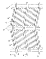
〔実施例6〕図13,図15は、共通電極が走査信号配線と交差して2行にわたり屈曲して配置されている構造の平面図である。一画素単位で交差しているが2画素以上の単位で交差していても良い。理想的なドット反転駆動方式を採用する場合には、図13,図15にあるような配置となる。
図19,図20は、奇数群と偶数群に分離した共通電極に走査信号の周期にあわせて、それぞれ逆相の電圧信号波形を印加し、かつ奇数群、偶数群の共通電極に対向している液晶駆動電極に、共通電極とは、逆相の映像信号波形をそれぞれ印加する駆動電圧波形図である.この駆動方式では水平クロストークが発生しなくなり良好な画像が得られる。
映像信号波形と逆相の電圧を共通電極に印加することで、液晶相に大きな電圧を印加できるので、共通電極電位を固定していた従来のドット反転駆動の場合の映像信号駆動振幅よりも1/2以下に低減が可能となる。これにより安価な5V駆動のICを使用することができるのでコストdownが可能となる。
【0046】
〔実施例7〕図14,図16は、走査信号配線と交差して2行にわたり屈曲して配置されている共通電極をそれぞれ別々に分離した構造の平面図である。走査信号配線と映像信号配線と別々に分離された共通電極の3種類の電極が静電気対策用非線形素子により外周部の静電気対策用連結電極に接続されている。図21,図22は、別々に分離独立した共通電極にフィールド周期ごとに印加電圧極性を変化させ、かつ屈曲した共通電極に対向している液晶駆動電極に、共通電極とは逆相の映像信号電圧波形を、それぞれ印加する駆動電圧波形図である。本発明のように共通電極を別々に分離し、それぞれ固有の電圧波形を印加することで共通電極の極性変化のタイミングに関する条件が非常にゆるやかなものになる。走査信号配線がONする前であれば数本前の走査信号配線にあわせて極性を切り変えれば良い。切り変えの電圧波形がゆっくり変化しても良いことになり、共通電極の金属材料の選択の自由度が大幅に拡大する.共通電極の配線抵抗の問題がなくなってしまうのである.
図21,図22は、一番基本的な共通電極の駆動波形であり、フィールド周期ごとに共通電極の電位の極性変化があれば駆動波形としては十分であり、フィールド極性変化が生じてからの次のフィールド極性変化が生じるまでの期間の電圧波形は、まったく自由であり周波数に制限はない。
【0047】
〔実施例8〕図17は、共通電極を奇数群と偶数群に分離し、走査信号周期にあわせて、それぞれ逆相の電圧信号波形を印加し、かつ奇数群、偶数群の共通電極に対向している液晶駆動電極に共通電極とは逆相の映像信号波形をそれぞれ印加するものである。実施例6とは異なり走査信号配線は同時に2本ONする駆動方式になっている.この構造でも映像信号配線の奇数番の偶数番では極性の異なる映像信号電圧を印加するので、クロストークの生じない画像を実現できる.カラーフィルターの色の配置としてデルタ配列を実現できるので混色の良い画像が得られる。
【0048】
〔実施例9〕図18は、共通電極をそれぞれ別々に分離した構造の平面図である。走査信号配線と映像信号配線とそれぞれ別々に分離された共通電極の3種類の電極が静電気対策用非線形素子により外周部の静電気対策用連結電極に接続されている.図18の構造の場合実施例7とは異なり走査信号配線は同時に2本ONする駆動方式になっている。動作原理は実施例7とほとんど同じものを適用できる。
【0049】
〔実施例10〕図28,図35は、一本の走査信号配線をはさんだ前後2行にわたり、薄膜トランジスタが交互に液晶駆動電極と接続されており、液晶駆動電極に対向している共通電極は、それぞれ各行ごとに分離独立している構造の平面図である。図29,30は、それぞれ各行ごとに分離独立している共通電極にフィールド周期の2倍の周期で信号電圧を印加し、フィールド周期ごとに印加電圧極性を変化させ、かつ共通電極に対向している液晶駆動電極に、共通電極とは逆相の映像信号電圧波形をそれぞれ印加する駆動電圧波形図である.動作原理は実施例7と同じである。
【0050】
〔実施例11〕図23は従来アルミニウム電極を走査信号配線として用いる時の断面図である。アルミニウムのヒロック防止のために高融点金属▲29▼をキャップメタルとして用いている。アルミニウムの側壁の傾面の長さが1μm以上長くなると側壁からヒロックが発生する。これを防止するためにネオジウムなどの金属を1〜2アトミックパーセント程度混入させる方法がある。しかしアルミニウムの合金ターゲットを大面積で作ることは非常にむずかしく均一な組成を作ることは不可能にちかい。純アルミニウムを走査信号配線として使用することは、大画面の液晶表示パネルを作るうえで非常に重要なことである。本発明では純アルミニウムのサイドヒロックを防止するために、高温水蒸気酸化法を用いてアルミニウムの側壁に酸化アルミニウムを形成している。図24がそれの断面図である。他の方法としては、イオンインプランテーション技術を用いて、酸素イオンや窒素イオン、リンイオンなどを高融点金属とアルミニウムの側壁にイオン注入することでサイドヒロックを防止することも可能である。
【0051】
〔実施例12〕図25は、横電界方式の液晶表示装置のカラーフィルター基板の断面図である.ガラス基板の上にBM(ブラックマスク)を形成し次にカラーフィルター層を形成する。ガラス基板には0.1〜1.0%程度のアルカリ金属酸化物が混入されている.さらにカラーフィルター層の顔料や染料などは、多くの不純物を含有し、これらの可動イオン物質は、電界が存在すれば電界の方向にしたがって移動する性質をもっている。平担化のためのオーバーコート層▲41▼は、有機物のものがおもに用いられているが、この膜には、可動イオンの電界移動を防止する能力はない.可動イオンのパッシベーション膜としてよく用いられる膜として、窒化シリコン膜や酸窒化シリコン膜、酸化アルミニウム膜がある.本発明では、図25にあるようにこれらのパッシベーション膜をプラズマCVD技術やスパッタリング技術を用いてカラーフィルター層の上に形成することで、可動イオンが液晶層や配向膜表面まで移動することを防止している.この構造により横電界がカラーフィルター層やガラス基板にまで作用してもパッシベーション膜▲40▼によって可動イオンの流出は防止できる.これにより配向膜の配向不良や、残像問題が発生しなくなる。
【0052】
〔実施例13〕図26,図27は、横電界方式の液晶表示装置のカラーフィルター基板の断面図と平面図である。液晶セル工程でのラビング処理プロセスで配向膜上に静電気が発生し、いろいろなトラブルの原因となっている。本発明では、オーバーコート層▲41▼の上に導電性の電極をメッシュ状または、ストライプ状に形成しこの電位をTFT基板側の映像信号電圧の中間値付近に設定することで、外部からの静電気の電界の影響を遮断している.オーバーコート層の上の導電性の電極の幅をBM幅よりも小さくすることでカラーフィルター基板と、TFT基板のアライメント精度が悪るい場合でもTFT基板の液晶駆動電極に悪影響が出ないようにしている。
【0053】
〔実施例14〕図5にあるように、液晶駆動電極と共通電極の電極間距離が1画素内ですべて均一でなく2種類以上の電極間距離の組み合せで形成されている。映像信号配線に一番近い電極間距離を一番大きくすることで映像信号配線の影響を低減することが可能となり、垂直ストロークを低減することが可能となる.本発明の屈曲電極構造と組み合せることカラーシフトがなくクロストークのない最高の画像が得られる.
【0054】
【発明の効果】
本発明によれば、第1に、画像の階調反転がなく、どこから見てもカラーシフトの生じない視角特性の良好な画像が得られる.第2に、ディスクリネーションの発生しないしかも残像の生じないコントラストの良い信頼性の高い画像表示装置を作れる.第3に、映像信号駆動ICに安価な5VICを利用でき、従来の液晶部材を使用できるので、コストの安い、生産性の高い画像表示装置を提供できる。第5に、超大型大画面液晶表示装置を従来の金属材料を用いて実現することが可能となる。
【図面の簡単な説明】
【図1】 従来のディスクリネーション発生防止対策電極構造の平面図
【図2】 従来の直線状画素電極と正の誘電率異方性液晶の配向図
【図3】 従来のディスクリネーション発生防止対策電極構造の平面図
【図4】 従来の直線状画素電極と負の誘電率異方性液晶の配向図
【図5】 本発明の横電界方式薄膜半導体基板の単位画素の平面図
【図6】 本発明の横電界方式薄膜半導体基板の単位画素の平面図
【図7】 本発明の横電界方式薄膜半導体基板の単位画素の平面図
【図8】 本発明の横電界方式薄膜半導体基板の単位画素の平面図
【図9】 本発明の横電界方式薄膜半導体基板の単位画素の平面図
【図10】 本発明の横電界方式薄膜半導体基板の単位画素の平面図
【図11】 本発明の横電界方式薄膜半導体基板の単位画素の断面図
【図12】 本発明の横電界方式薄膜半導体基板の単位画素の断面図
【図13】 本発明の横電界方式薄膜半導体基板の画素配列の平面図
【図14】 本発明の横電界方式薄膜半導体基板の画素配列の平面図
【図15】 本発明の横電界方式薄膜半導体基板の画素配列の平面図
【図16】 本発明の横電界方式薄膜半導体基板の画素配列の平面図
【図17】 本発明の横電界方式薄膜半導体基板の画素配列の平面図
【図18】 本発明の横電界方式薄膜半導体基板の画素配列の平面図
【図19】 本発明の横電界方式液晶表示装置の駆動電圧波形図
【図20】 本発明の横電界方式液晶表示装置の駆動電圧波形図
【図21】 本発明の横電界方式液晶表示装置の駆動電圧波形図
【図22】 本発明の横電界方式液晶表示装置の駆動電圧波形図
【図23】 従来の走査信号配線の断面図
【図24】 従来の走査信号配線の断面図
【図25】 本発明の横電界方式液晶表示装置用カラーフィルターの断面図
【図26】 本発明の横電界方式液晶表示装置用カラーフィルターの断面図
【図27】 本発明の横電界方式液晶表示装置用カラーフィルターの平面図
【図28】 本発明の横電界方式薄膜半導体基板の画素配列の平面図
【図29】 本発明の横電界方式液晶表示装置の駆動電圧波形図
【図30】 本発明の横電界方式液晶表示装置の駆動電圧波形図
【図31】 本発明のディスクリネーション発生防止対策電極の構造の平面図と正の誘電率異方性液晶の配向図
【図32】 本発明のディスクリネーション発生防止対策電極の構造の平面図と負の誘電率異方性液晶の配向図
【図33】 本発明の横電界方式薄膜半導体基板の単位画素の平面図
【図34】 本発明の横電界方式薄膜半導体基板の単位画素の平面図
【図35】 本発明の横電界方式薄膜半導体基板の画素配列の平面図
【図36】 本発明の横電界方式薄膜半導体基板の単位画素の平面図
【符号の説明】
1――走査信号配線
2――映像信号配線
3――共通電極
4――液晶駆動電極
5――薄膜トランジスタ(TFT)素子
6――TFT基板側液晶配向軸
7――正の誘電率異方性液晶分子(P型液晶分子)と画素電極(共通電極と液晶駆動電極)の交差する角度
8――負の誘電率異方性液晶分子(N型液晶分子)と画素電極(共通電極と液晶駆動電極)の交差する角度
9――正の誘電率異方性液晶分子(P型液晶分子)
10――負の誘電率異方性液晶分子(N型液晶分子)
11――TFT側ガラス基板
12――半導体層
13――不純物をドープしたn+アモリファスシリコン層
14――配向膜
15――奇数番共通電極駆動用連結電極
16――偶数番共通電極駆動用連結電極
17――静電気対策用素子
18――走査信号配線引き出し端子
19――映像信号配線引き出し端子
20――共通電極引き出し端子
21――静電気対策用連結電極
22――n番走査信号配線駆動波形
23――奇数番共通電極駆動波形
24――奇数番映像信号波形
25――(n+1)番走査信号配線駆動波形
26――偶数番映像信号波形
27――偶数番共通電極駆動波形
28――アルミニウム(orアルミニウム合金)走査信号配線
29――高融点金属(or高融点金属のシリサイド化合物、高融点金属化合物)
30――側壁酸化アルミニウム
31――(n−1)番走査信号配線駆動波形
32――m番共通電極駆動波形(直線接続型)
33――m番共通電極駆動波形
34――(m+1)番共通電極駆動波形(直線接続型)
35――静電気対策用連結電極引き出し端子
36――(m−1)番共通電極駆動波形
37――(m+1)番共通電極駆動波形
38――ブラックマスク
39――カラーフィルター層
40――カラーフィルターパッシベーション膜
41――平担化膜
42――静電気対策用導電性膜(or半導体膜)
43――カラーフィルター側液晶配向膜
44――下地絶縁膜
45――ゲート絶縁膜
46――TFTパッシベーション膜
47――カラーフィルター側ガラス基板
48――ドレインスルーホール[0001]
[Industrial application fields]
The present invention relates to a large-screen active matrix liquid crystal display device with a wide viewing angle and high image quality.
[0002]
[Prior art]
A method of applying an electric field to a liquid crystal composition layer using a comb-like electrode pair formed on one substrate of a conventional active matrix liquid crystal display device is disclosed in, for example, Japanese Patent Application Laid-Open Nos. 7-36058 and 7-159786. And JP-A-6-160878 and JP-A-7-191336. Hereinafter, a display method in which a main electric field direction applied to the liquid crystal composition layer is a direction substantially parallel to the substrate interface is referred to as a horizontal electric field method.
1 and 3 show an example of a conventional horizontal electric field method. The liquid crystal drive electrode (4) and the common electrode (3), which are comb-like pixel electrodes, are linearly arranged in parallel. At the center of the pixel and the periphery of the pixel, the shape of the liquid crystal drive electrode and the common electrode is made so that the electric field distribution in the pixel electrode has a shape in which the center of the pixel is rotationally symmetric.
As shown in FIGS. 2 and 4, the rotational movement direction of the liquid crystal molecules is only in one direction within one pixel.
[0003]
[Problems to be solved by the invention]
In a horizontal electric field type liquid crystal panel in which the pixel electrode is linear and the rotational movement direction of liquid crystal molecules is only one direction, there is a problem of color shift when the left and right colors appear different when viewed from the horizontal direction. Further, when the pretilt angle of the liquid crystal is increased by 3 degrees or more, the viewing angle characteristic is deteriorated, and the gradation reversal phenomenon in the halftone region occurs, resulting in a very unnatural image display.
[0004]
A horizontal electric field type liquid crystal panel with a bent pixel electrode has also been proposed, but only the electric field around the bent portion and the pixel has caused a large number of disclination defects, and the black level is greatly deteriorated. Unevenness occurs.
[0005]
On the side of the horizontal electric field type active matrix substrate, the area of the intersection of the common electrode and the liquid crystal drive electrode is large, and if there is a defect such as a pinhole in the insulating film, it will be short-circuited and likely to become a pixel defect. In order to reduce the process cost, a method of simultaneously forming the scanning signal wiring and the common electrode is used. In this process, since there are so many areas where the scanning signal wiring and the common electrode are close to each other, when a pattern defect occurs, a short circuit between the scanning signal wiring and the common electrode cannot be avoided and the yield is very bad. Rui.
[0006]
In the liquid crystal display device of the horizontal electric field type, the liquid crystal driving voltage tends to be higher than that of the conventional vertical electric field type TN liquid crystal display device, and the driver IC for driving is required to have a high voltage output, resulting in a high cost. was there.
[0007]
In the horizontal electric field type liquid crystal display device, the electric field of the liquid crystal drive electrode and the common electrode enters the glass substrate and color filter layer on the color filter side, so that the movable ionic substance contained in the glass substrate and the color filter layer is over. It passes through the coating layer and elutes into the alignment film and the liquid crystal. These mobile ionic substances cause afterimages and pretilt angle abnormalities, resulting in unevenness and severely worsening the image quality.
[0008]
Also, the horizontal electric field type color filter substrate, like the conventional vertical electric field type TN liquid crystal display device, does not have a transparent conductive film on the entire surface. There is a problem.
[0009]
The present invention has been made to solve these problems, and an object of the present invention is to provide a liquid crystal display device which has no gradation inversion, good viewing angle characteristics, and good contrast without causing color shift. . Furthermore, a low voltage driving IC can be used, which improves the yield of the liquid crystal process and reduces the cost.
[0010]
[Means for Solving the Problems]
In order to solve the above problems and achieve the above object, the present invention uses the following means.
A scanning signal line and a video signal line on a substrate, a thin film transistor formed at each intersection of the scanning signal line and the video signal line, a liquid crystal drive electrode connected to the thin film transistor, and at least a part of the liquid crystal A liquid crystal display device comprising an active matrix substrate having a common electrode formed to face a drive electrode, a counter substrate facing the active matrix substrate, and a liquid crystal layer sandwiched between the active matrix substrate and the counter substrate In
[Means 1] The liquid crystal driving electrode and the common electrode facing the liquid crystal driving electrode are bent with respect to the alignment direction of the liquid crystal molecules. In the peripheral part of the pixel, each electrode bends in the direction of the concave part of the bend, and the electric field distribution formed by the liquid crystal drive electrode and the common electrode facing the liquid crystal drive electrode is the center of the pixel. Was distributed with the line symmetry axis.
[0011]
[Means 2] The liquid crystal driving electrode and the common electrode facing the liquid crystal driving electrode are bent at a pixel period with respect to the alignment direction of the liquid crystal molecules, and the peripheral electrode in each pixel in the bent convex direction. The electric field distribution formed by the liquid crystal driving electrode and the common electrode facing the liquid crystal driving electrode is bent and distributed with the scanning signal wiring as the line symmetry axis or the video signal wiring as the line symmetry axis. I tried to become.
[0012]
[Means 3] The liquid crystal molecules are prevented from including a chiral dopant material so that both the left rotation and the right rotation can be rotated with the same rotational force.
[0013]
[Means 4] In the
[0014]
[Means 5] In the horizontal electric field type liquid crystal display device, the common electrode and the liquid crystal driving electrode are separated from each other by two or more insulating films.
[0015]
[Means 6] In the horizontal electric field type liquid crystal display device, the common electrode is arranged so as to be bent over two rows crossing the scanning signal wiring.
[0016]
[Means 7] In the
[0017]
[Means 8] In the means 7, the common electrodes are separated into an odd group and an even group, and each is connected to an odd-numbered common electrode driving connecting electrode and an even-numbered common electrode driving connecting electrode. A driving method that applies a signal voltage waveform of a phase opposite to that of the common electrode to the liquid crystal drive electrode facing the common electrode of the odd-numbered group and the even-numbered group. It was.
[0018]
[Means 9] In the
[0019]
[Means 10] In the
[0020]
[Means 11] In a horizontal electric field type liquid crystal display device, a thin film transistor is alternately connected to a liquid crystal drive electrode across two rows before and after a single scanning signal wiring, and a common electrode facing the liquid crystal drive electrode Are arranged in a separate and independent manner for each row.
[0021]
[Means 12] In the means 11, a signal voltage is applied to a common electrode separated and independent for each row at a frequency that is an integral multiple of 1/2 of the field frequency, and the polarity of the applied voltage is changed for each field period. In addition, a driving method is applied in which a video signal voltage waveform having a phase opposite to that of the common electrode is applied to the liquid crystal drive electrode facing the common electrode.
[0022]
[Means 13] In the
[0023]
[Means 14] In the active matrix substrate liquid crystal display device, the scanning signal wiring is formed of two layers of aluminum and a refractory metal, and the refractory metal is covered on the aluminum, and the side wall on which the refractory metal is not covered. In addition, aluminum oxide was formed on the exposed portions of aluminum near the side walls.
[0024]
[Means 15] In a horizontal electric field type liquid crystal display device, after forming a passivation film such as a silicon nitride film, a silicon oxide film or an aluminum oxide film on the color filter layer, an overcoat layer for flattening is formed. A counter substrate having a structure in which is formed on a passivation film was used.
[0025]
[Means 16] In the means 15, a conductive electrode is formed in a mesh shape or a stripe shape on the overcoat layer formed on the passivation film, and this potential is in the vicinity of an intermediate value of the video signal voltage on the TFT substrate side. Can be set to
[0026]
[Means 17] In the means 15, the pattern width of the conductive electrode formed in a mesh shape or stripe shape on the overcoat layer is made smaller than the width of the underlying BM (black mask).
[0027]
[Means 18] In the
[0028]
[Action]
When the horizontal electric field is applied in the pixel electrode (a part of the liquid crystal drive electrode and the common electrode) by the above means 1 and 3 as shown in FIGS. 31 and 32, the liquid crystal molecules are rotated left inside the pixel electrode. Performs two types of rotation, right rotation.
As shown in FIGS. 2 and 4, in the conventional lateral electric field method, since the rotational movement is only in one direction, a color shift in which the color changes depending on the viewing direction occurs. Further, when the pretilt angle of the liquid crystal is large, the viewing angle characteristic is shifted, and the gradation inversion in the halftone area is likely to occur. If two types of rotation, left rotation and right rotation, are possible within one pixel, all the above problems are solved. However, if the rotational forces of the left rotation and the right rotation are not equalized, the liquid crystal moves at the bent portion of the central portion of the pixel electrode, resulting in a large disclination defect. Further, even in a portion where the electric field in the peripheral portion of the pixel is leaked, the rotation of the liquid crystal becomes abnormal and a disclination defect occurs. These alignment defects of the liquid crystal remain in the generated portion once the response speed is once generated. This may appear as an afterimage. The disclination defect portion leaks light even when black is displayed, and the contrast is drastically lowered. By using the
[0029]
By using the above means 2 and 3, the rotational movement direction of the liquid crystal molecules in one pixel causes the two rotational movements of the left rotation and the right rotation in the whole screen even if the rotation movement direction of the liquid crystal molecules is one direction. Is possible. This effect can solve all of the color shift problem, the tone reversal problem of the halftone area, and the deviation problem of the viewing angle characteristic. Since the occurrence of disclination defects can be prevented by aligning only the electric field around the pixels in the direction of rotation of the liquid crystal, it is possible to completely prevent a decrease in contrast and the occurrence of afterimages.
[0030]
By using the above means 1, 2 and 4, the storage capacity of the liquid crystal drive electrode can be increased, and the storage capacity decreases even if the bulk area around the pixel of the common electrode and the liquid crystal drive electrode is reduced. Can be resolved. As a result, the aperture ratio of the pixel can be increased, and the light utilization efficiency is improved.
[0031]
By using the
[0032]
By using the
[0033]
By using the
[0034]
By using the means 11 and 12, the same effect as when the
[0035]
By using the
[0036]
By using the means 14, the side lock is not generated even when inexpensive and low resistance aluminum is used for the scanning signal wiring, and the yield can be improved.
[0037]
By using the means 15, 16 and 17, it is possible to prevent a mobile ionic substance such as sodium contained in the glass substrate from eluting into the liquid crystal through the overcoat layer, and to prevent the afterimage problem. Can be suppressed. Since the decrease in the specific resistance value of the liquid crystal can be prevented, a highly reliable liquid crystal panel having a high charge retention rate can be manufactured. Uniform and good halftone display is possible because unevenness and reduction in contrast can be prevented. Static electricity can be prevented and dust is less deposited.
[0038]
By using the above means 1, 2 and 18, it is possible to prevent gradation inversion even if the photomask is slightly misaligned, and it is possible to obtain a good image that is less than the viewing angle characteristic and hardly causes color shift. it can.
[0039]
【Example】
[Embodiment 1] FIGS. 5, 6, 7, 8, 9, 10, 11, and 12 are a plan view and a sectional view of a unit pixel of the present invention. The cross-sectional views of FIGS. 5, 6, and 9 are FIG. 11, and the cross-sectional views of FIGS. 7, 8, and 10 are FIG. The scanning signal wiring is preferably made of an anodizable metal such as Al, but may be a pure metal or alloy such as Cr, Mo, Ti, W, Ta, or Nb. A two-layer structure or a three-layer structure of Cu or Al having a low electrical resistance value as a main material and the refractory metal or an alloy of the refractory metal is used in an ultra-large display device. In the case of FIG. 5, FIG. 6 and FIG. 9, the scanning signal wiring (1) and the common electrode (3) can be formed simultaneously in the same layer. Since the short circuit with (3) occurs frequently, the scanning signal wiring (1) and the common electrode (3) are separated into different layers as shown in FIGS. Thereby, even if a pattern defect occurs, a short circuit is not caused, so that the yield can be greatly improved. In the case of FIGS. 7, 8, and 10 as well, by separating the video signal wiring (2) and the common electrode (3) into different layers, a short circuit does not occur even if a pattern defect occurs, so that the yield is improved. improves. A gate insulating film (45) is formed on the scanning signal wiring (1), and then an amorphous silicon film layer (12) is formed as an active active layer of the transistor. A polysilicon film layer may be used instead of an amorphous silicon film. A composite laminated film of a polysilicon film and an amorphous film is equally good. N doped with an impurity such as phosphorus on the active active layer + An amorphous silicon layer is formed. Next, a video signal wiring and a drain electrode are formed so as to overlap a part of the active active layer. In the case of FIGS. 5, 6, 7, 8, 9, and 10, the drain electrode and the liquid crystal drive electrode (4) are simultaneously formed of the same metal material. As shown in FIG. 34, after forming the passivation film after forming the drain electrode, it is also possible to open the drain through hole and electrically connect the drain electrode and the liquid crystal driving electrode. After forming the passivation film, in FIG. 11, an alignment film (14) made of polyimide is formed, and the surface is rubbed. Similarly, a liquid crystal composition containing rod-like liquid crystal molecules (9) and (10) is encapsulated between a counter substrate (47) on which an alignment film (43) having a rubbing treatment is formed on the surface and the active matrix substrate. A polarizing plate is arranged on the outer surface of the two substrates to complete the liquid crystal cell in the transverse electric field direction.
[0040]
The basic conceptual diagram of the present invention is shown in FIGS. FIG. 31 shows the layout of the liquid crystal drive electrode (4) and the common electrode (3) when using a positive dielectric anisotropy liquid crystal (9) and the relationship between the rubbing alignment axis direction (6) with respect to these electrodes. Is shown.
FIG. 32 shows the layout of the liquid crystal drive electrode (4) and the common electrode (3) when the negative dielectric anisotropy liquid crystal (10) is used, and the relationship between the rubbing alignment axis direction (6) with respect to these electrodes. Is shown. As shown in FIGS. 1 and 3, the conventional electrode shape arrangement is an electrode shape with the center of the pixel being rotationally symmetric, but in the case of the present invention, the electrode shape having the center axis of the pixel as the axis of line symmetry. It becomes. In the bent portion at the center of the pixel, each electrode protrudes in the direction of the bent convex portion, and in the peripheral portion of the pixel, each electrode is bent in the bent concave portion direction. The number of bends may be one bend as shown in FIGS. 31 and 32 in one pixel, or two or more bends. The orientation method may not be a rubbing method. An alignment method using a UV alignment film may be used. In the case of the present invention, since there are two directions of rotation of the liquid crystal molecules in one pixel in one pixel, no color shift occurs in principle. For this reason, a conventional unidirectionally rotating lateral electric field type liquid crystal panel cannot reduce the color shift without using a liquid crystal having a small refractive index anisotropy Δn, but the value of Δn can be reduced by using the electrode of the present invention. It became possible to set freely. Since Δn can be increased, the drive voltage can also be reduced. The alignment film can also be selected without being governed by the pretilt angle.
[0041]
[Embodiment 2] In FIGS. 33 and 34, the liquid crystal drive electrode and the common electrode are bent with a pixel period with respect to the alignment direction of the liquid crystal molecules, and the peripheral electrode in each pixel is placed in the convex direction of the bend. The electric field distribution formed by the bent liquid crystal driving electrode and the common electrode facing the liquid crystal driving electrode is a distribution with the scanning signal wiring as the line target axis or the video signal wiring with the line symmetry axis. It is a top view of the unit pixel in the case. A set of two adjacent pixels expresses the same function as the unit pixel of the first embodiment. Although the electrode structure of Example 1 is necessary for a computer display, the electrode structure shown in FIGS. 33 and 34 is sufficient when displaying a moving image such as a television. 33 and 34 have a structure in which the common electrode is arranged in parallel without crossing the scanning signal wiring. This is the same arrangement as in FIG. 5, FIG. 6 and FIG. 9 in the first embodiment. As shown in FIGS. 7, 8, and 10, a structure arranged in parallel without crossing the video signal wiring is also possible. The liquid crystal driving electrode and the common electrode in one pixel in FIG. 33 are not bent in one pixel unlike FIGS. 5 and 6, and thus the light transmittance can be increased.
[0042]
[Embodiment 3] As described in
[0043]
[Embodiment 4] FIG. 7, FIG. 8, FIG. 10, FIG. 36, and FIG. 12 are a plan view and a cross section of a structure in which a part of a liquid crystal driving electrode is sandwiched by covering an insulating film with a scanning signal wiring and a common electrode. FIG. With this structure, the storage capacity of the liquid crystal drive electrode can be increased, so that the bulk area of the common electrode and the liquid crystal drive electrode within the effective pixel can be reduced. This can enlarge the aperture ratio of the pixel. In the case of FIG. 36, since the video signal wiring and the common electrode intersect with each other through the passivation film (46), the passivation film (46) is 1.5 times larger than that of the structure of FIGS. It is necessary to make it about twice as thick. By forming a passivation film with a thickness of about 4000 to 6000 mm by using a plasma CVD apparatus in two steps, a short circuit due to a pinhole can be drastically reduced.
[0044]
[Embodiment 5] FIG. 5, FIG. 6, FIG. 9, and FIG. 11 are a plan view and a sectional view of a structure in which a common electrode and a liquid crystal drive electrode are separated by two or more insulating films. First, a common electrode (3) is formed on a glass substrate (11), and then a base insulating film (44) is deposited using a plasma CVD apparatus. Next, a scanning signal wiring (1) is formed, a gate insulating film (45) is deposited, and then a semiconductor layer (12) and an impurity doped n + An amorphous silicon layer is continuously formed. The liquid crystal drive electrode (4) and the video signal wiring (2) are formed simultaneously using the same metal material. After depositing a passivation film (46) on these, a liquid crystal alignment film (14) is formed by flexographic printing. As can be seen from the cross-sectional view of FIG. 11, the common electrode (3) and the liquid crystal drive electrode (4) are separated from each other by two insulating films. This structure can also be applied to the conventional electrode
[0045]
[Embodiment 6] FIGS. 13 and 15 are plan views of a structure in which the common electrode is arranged to bend over two rows crossing the scanning signal wiring. Although it intersects in units of one pixel, it may intersect in units of two or more pixels. When the ideal dot inversion driving method is adopted, the arrangement is as shown in FIGS.
19 and 20, voltage signals having opposite phases are applied to the common electrodes separated into the odd-numbered group and the even-numbered group in accordance with the period of the scanning signal, and are opposed to the odd-numbered group and even-numbered group common electrodes. The common electrode is a drive voltage waveform diagram that applies the video signal waveform of opposite phase to the liquid crystal drive electrode. With this driving method, horizontal crosstalk does not occur and a good image can be obtained.
Since a large voltage can be applied to the liquid crystal phase by applying a voltage having a phase opposite to that of the video signal waveform to the common electrode, the amplitude is 1 than the video signal driving amplitude in the case of the conventional dot inversion driving in which the common electrode potential is fixed. / 2 or less can be reduced. As a result, an inexpensive 5V driving IC can be used, so that the cost can be reduced.
[0046]
[Embodiment 7] FIGS. 14 and 16 are plan views of structures in which common electrodes arranged so as to be bent over two rows intersecting with scanning signal wirings are separately separated. Three types of electrodes, that is, a common electrode separated separately from the scanning signal wiring and the video signal wiring, are connected to the electrostatic countermeasure connection electrode on the outer peripheral portion by a static countermeasure nonlinear element. FIGS. 21 and 22 show video signals having phases opposite to those of the common electrode in the liquid crystal drive electrode facing the bent common electrode while changing the applied voltage polarity to the common electrode separately separated and independent for each field period. It is a drive voltage waveform figure which applies a voltage waveform, respectively. By separating the common electrodes separately and applying a unique voltage waveform as in the present invention, the conditions relating to the timing of the polarity change of the common electrode become very gentle. Before the scanning signal wiring is turned on, the polarity may be switched according to the scanning signal wiring several lines before. The switching voltage waveform may change slowly, which greatly expands the degree of freedom in selecting the metal material for the common electrode. This eliminates the problem of the wiring resistance of the common electrode.
FIGS. 21 and 22 show the most basic driving waveform of the common electrode. If there is a change in the polarity of the potential of the common electrode for each field period, the driving waveform is sufficient. The voltage waveform in the period until the next field polarity change occurs is completely free and there is no limit on the frequency.
[0047]
[Embodiment 8] FIG. 17 shows that the common electrodes are separated into an odd group and an even group, and voltage signal waveforms having opposite phases are applied in accordance with the scanning signal period, and the common electrodes of the odd group and even group are opposed to each other. A video signal waveform having a phase opposite to that of the common electrode is applied to the liquid crystal drive electrodes. Unlike Example 6, the scanning signal wiring is a drive system in which two lines are turned on simultaneously. Even in this structure, video signals with different polarities are applied to odd and even numbers of video signal wiring, so that an image without crosstalk can be realized. Since a delta arrangement can be realized as the color arrangement of the color filters, an image with good color mixing can be obtained.
[0048]
[Embodiment 9] FIG. 18 is a plan view of a structure in which common electrodes are separated separately. Three types of electrodes, the common electrode separately separated from the scanning signal wiring and the video signal wiring, are connected to the antistatic connection electrode on the outer periphery by a non-static element for electrostatic countermeasures. In the case of the structure of FIG. 18, unlike the seventh embodiment, the drive system is such that two scanning signal lines are simultaneously turned on. The operation principle is almost the same as that of the seventh embodiment.
[0049]
[Embodiment 10] In FIGS. 28 and 35, thin film transistors are alternately connected to a liquid crystal drive electrode over two rows before and after one scanning signal wiring, and a common electrode facing the liquid crystal drive electrode is shown in FIG. FIG. 3 is a plan view of a structure in which each row is separated and independent. In FIGS. 29 and 30, a signal voltage is applied to a common electrode separated and independent for each row at a period twice the field period, the applied voltage polarity is changed for each field period, and the common electrode is opposed to the common electrode. It is a drive voltage waveform diagram that applies the video signal voltage waveform in the opposite phase to the common electrode to the liquid crystal drive electrode. The operating principle is the same as in the seventh embodiment.
[0050]
[Embodiment 11] FIG. 23 is a sectional view when a conventional aluminum electrode is used as a scanning signal wiring. In order to prevent hillocks in aluminum, refractory metal (29) is used as a cap metal. When the length of the inclined surface of the aluminum side wall becomes longer than 1 μm, hillocks are generated from the side wall. In order to prevent this, there is a method in which a metal such as neodymium is mixed by about 1 to 2 atomic percent. However, it is very difficult to make an aluminum alloy target with a large area, and it is impossible to make a uniform composition. The use of pure aluminum as the scanning signal wiring is very important in making a large-screen liquid crystal display panel. In the present invention, in order to prevent side hillocks of pure aluminum, aluminum oxide is formed on the side walls of aluminum using a high temperature steam oxidation method. FIG. 24 is a sectional view thereof. As another method, it is also possible to prevent side hillocks by ion implantation of oxygen ions, nitrogen ions, phosphorus ions, or the like into the side walls of the refractory metal and aluminum using an ion implantation technique.
[0051]
[Embodiment 12] FIG. 25 is a sectional view of a color filter substrate of a horizontal electric field type liquid crystal display device. A BM (black mask) is formed on the glass substrate, and then a color filter layer is formed. About 0.1 to 1.0% alkali metal oxide is mixed in the glass substrate. Furthermore, the pigments and dyes of the color filter layer contain many impurities, and these mobile ionic substances have the property of moving according to the direction of the electric field when an electric field is present. The overcoat layer (41) for flattening is mainly made of organic material, but this film does not have the ability to prevent electric field movement of mobile ions. Examples of films that are often used as mobile ion passivation films include silicon nitride films, silicon oxynitride films, and aluminum oxide films. In the present invention, as shown in FIG. 25, these passivation films are formed on the color filter layer using the plasma CVD technique or the sputtering technique to prevent the mobile ions from moving to the liquid crystal layer or the alignment film surface. is doing. With this structure, even if a lateral electric field acts on the color filter layer and the glass substrate, the outflow of mobile ions can be prevented by the passivation film (40). Thereby, the alignment defect of the alignment film and the afterimage problem do not occur.
[0052]
[Embodiment 13] FIGS. 26 and 27 are a sectional view and a plan view of a color filter substrate of a liquid crystal display device of a horizontal electric field type. Static electricity is generated on the alignment film during the rubbing process in the liquid crystal cell process, causing various troubles. In the present invention, a conductive electrode is formed on the overcoat layer (41) in a mesh shape or a stripe shape, and this potential is set near the intermediate value of the video signal voltage on the TFT substrate side. Blocks the effects of static electric fields. By making the width of the conductive electrode on the overcoat layer smaller than the BM width, the liquid crystal drive electrode of the TFT substrate is not adversely affected even when the alignment accuracy between the color filter substrate and the TFT substrate is poor. Yes.
[0053]
[Embodiment 14] As shown in FIG. 5, the distance between the liquid crystal drive electrode and the common electrode is not uniform within one pixel, but is formed by a combination of two or more kinds of distances between electrodes. By increasing the distance between the electrodes closest to the video signal wiring, the influence of the video signal wiring can be reduced and the vertical stroke can be reduced. In combination with the bent electrode structure of the present invention, the best image without color shift and crosstalk can be obtained.
[0054]
【The invention's effect】
According to the present invention, firstly, there is obtained an image having a good viewing angle characteristic in which there is no gradation inversion of the image and no color shift occurs from any position. Secondly, it is possible to produce a reliable and reliable image display device with no disclination and no afterimage. Third, since an inexpensive 5VIC can be used for the video signal driving IC and a conventional liquid crystal member can be used, an image display apparatus with low cost and high productivity can be provided. Fifth, it becomes possible to realize an ultra large large screen liquid crystal display device using a conventional metal material.
[Brief description of the drawings]
FIG. 1 is a plan view of a conventional electrode structure for preventing disclination.
FIG. 2 is an orientation diagram of a conventional linear pixel electrode and a positive dielectric anisotropy liquid crystal.
FIG. 3 is a plan view of a conventional electrode structure for preventing disclination.
FIG. 4 is an orientation diagram of a conventional linear pixel electrode and negative dielectric anisotropy liquid crystal.
FIG. 5 is a plan view of a unit pixel of a lateral electric field type thin film semiconductor substrate of the present invention.
FIG. 6 is a plan view of a unit pixel of a lateral electric field type thin film semiconductor substrate of the present invention.
FIG. 7 is a plan view of a unit pixel of a lateral electric field type thin film semiconductor substrate of the present invention.
FIG. 8 is a plan view of a unit pixel of a lateral electric field type thin film semiconductor substrate of the present invention.
FIG. 9 is a plan view of a unit pixel of a lateral electric field type thin film semiconductor substrate of the present invention.
FIG. 10 is a plan view of a unit pixel of a lateral electric field type thin film semiconductor substrate of the present invention.
FIG. 11 is a sectional view of a unit pixel of a lateral electric field type thin film semiconductor substrate of the present invention.
FIG. 12 is a sectional view of a unit pixel of a lateral electric field type thin film semiconductor substrate of the present invention.
FIG. 13 is a plan view of a pixel arrangement of a lateral electric field type thin film semiconductor substrate of the present invention.
FIG. 14 is a plan view of a pixel array of a lateral electric field type thin film semiconductor substrate of the present invention.
FIG. 15 is a plan view of a pixel arrangement of a lateral electric field type thin film semiconductor substrate of the present invention.
FIG. 16 is a plan view of a pixel arrangement of a lateral electric field type thin film semiconductor substrate of the present invention.
FIG. 17 is a plan view of a pixel array of a lateral electric field type thin film semiconductor substrate of the present invention.
FIG. 18 is a plan view of a pixel array of a lateral electric field type thin film semiconductor substrate of the present invention.
FIG. 19 is a drive voltage waveform diagram of the horizontal electric field mode liquid crystal display device of the present invention.
FIG. 20 is a drive voltage waveform diagram of the horizontal electric field mode liquid crystal display device of the present invention.
FIG. 21 is a drive voltage waveform diagram of the horizontal electric field mode liquid crystal display device of the present invention.
FIG. 22 is a drive voltage waveform diagram of the horizontal electric field mode liquid crystal display device of the present invention.
FIG. 23 is a sectional view of a conventional scanning signal wiring.
FIG. 24 is a sectional view of a conventional scanning signal wiring.
FIG. 25 is a cross-sectional view of a color filter for a horizontal electric field mode liquid crystal display device of the present invention.
FIG. 26 is a sectional view of a color filter for a horizontal electric field mode liquid crystal display device of the present invention.
FIG. 27 is a plan view of a color filter for a horizontal electric field mode liquid crystal display device of the present invention.
FIG. 28 is a plan view of a pixel array of a lateral electric field type thin film semiconductor substrate of the present invention.
FIG. 29 is a drive voltage waveform diagram of the horizontal electric field mode liquid crystal display device of the present invention.
FIG. 30 is a drive voltage waveform diagram of the horizontal electric field mode liquid crystal display device of the present invention.
FIG. 31 is a plan view of the structure of the electrode for preventing occurrence of disclination according to the present invention and an orientation diagram of positive dielectric constant anisotropic liquid crystal.
FIG. 32 is a plan view of the structure of the electrode for preventing occurrence of disclination according to the present invention and an orientation diagram of a negative dielectric constant anisotropic liquid crystal.
FIG. 33 is a plan view of a unit pixel of a lateral electric field type thin film semiconductor substrate of the present invention.
FIG. 34 is a plan view of a unit pixel of a lateral electric field type thin film semiconductor substrate of the present invention.
FIG. 35 is a plan view of a pixel array of a lateral electric field type thin film semiconductor substrate of the present invention.
FIG. 36 is a plan view of a unit pixel of a lateral electric field type thin film semiconductor substrate of the present invention.
[Explanation of symbols]
1-Scan signal wiring
2--Video signal wiring
3--Common electrode
4--LCD drive electrode
5--Thin Film Transistor (TFT) element
6—TFT substrate side liquid crystal alignment axis
7—An intersecting angle between positive dielectric anisotropy liquid crystal molecules (P-type liquid crystal molecules) and pixel electrodes (common electrode and liquid crystal drive electrode)
8—An intersecting angle between negative dielectric anisotropy liquid crystal molecules (N-type liquid crystal molecules) and pixel electrodes (common electrode and liquid crystal drive electrode)
9-Positive dielectric anisotropy liquid crystal molecules (P-type liquid crystal molecules)
10—Negative dielectric anisotropy liquid crystal molecules (N-type liquid crystal molecules)
11-TFT side glass substrate
12-Semiconductor layer
13-n doped with impurities + Amorphous silicon layer
14—Alignment film
15--Connecting electrode for driving odd-numbered common electrode
16--Connecting electrode for driving even-numbered common electrode
17—Anti-static element
18--Scan signal wiring lead-out terminal
19--Video signal wiring lead-out terminal
20-Common electrode lead-out terminal
21—Connecting electrode for static electricity countermeasures
22-nth scan signal wiring drive waveform
23-Odd number common electrode drive waveform
24-Odd number video signal waveform
25-(n + 1) th scan signal wiring drive waveform
26--even video signal waveform
27-Even-numbered common electrode drive waveform
28—Aluminum (or aluminum alloy) scanning signal wiring
29-Refractory metals (or refractory metal silicide compounds, refractory metal compounds)
30-side wall aluminum oxide
31-(n-1) scan signal wiring drive waveform
32--m common electrode drive waveform (straight connection type)
33-No. m common electrode drive waveform
34-(m + 1) common electrode drive waveform (straight line connection type)
35--Connecting electrode lead-out terminal for static electricity countermeasures
36-(m-1) common electrode drive waveform
37-(m + 1) common electrode drive waveform
38-Black Mask
39-Color filter layer
40-Color filter passivation film
41-Flattened membrane
42-Conductive film (or semiconductor film) for countermeasures against static electricity
43-Color filter side liquid crystal alignment film
44-Underlying insulating film
45--Gate insulation film
46-TFT passivation film
47--Color filter side glass substrate
48-drain through hole
Claims (6)
Priority Applications (2)
| Application Number | Priority Date | Filing Date | Title |
|---|---|---|---|
| JP33928197A JP3831863B2 (en) | 1997-10-21 | 1997-10-21 | Liquid crystal display |
| TW87117228A TW544538B (en) | 1997-10-21 | 1998-10-19 | Active matrix-type liquid crystal display device |
Applications Claiming Priority (1)
| Application Number | Priority Date | Filing Date | Title |
|---|---|---|---|
| JP33928197A JP3831863B2 (en) | 1997-10-21 | 1997-10-21 | Liquid crystal display |
Publications (2)
| Publication Number | Publication Date |
|---|---|
| JPH11125835A JPH11125835A (en) | 1999-05-11 |
| JP3831863B2 true JP3831863B2 (en) | 2006-10-11 |
Family
ID=18325973
Family Applications (1)
| Application Number | Title | Priority Date | Filing Date |
|---|---|---|---|
| JP33928197A Expired - Fee Related JP3831863B2 (en) | 1997-10-21 | 1997-10-21 | Liquid crystal display |
Country Status (2)
| Country | Link |
|---|---|
| JP (1) | JP3831863B2 (en) |
| TW (1) | TW544538B (en) |
Families Citing this family (46)
| Publication number | Priority date | Publication date | Assignee | Title |
|---|---|---|---|---|
| CN1321260A (en) * | 1999-09-01 | 2001-11-07 | 松下电器产业株式会社 | Liquid crystal display panel and method for producing same |
| JP4724339B2 (en) | 1999-09-07 | 2011-07-13 | 株式会社日立製作所 | Liquid crystal display |
| JP2001194685A (en) * | 2000-01-06 | 2001-07-19 | Hitachi Ltd | Liquid crystal display device |
| KR100338012B1 (en) * | 2000-07-27 | 2002-05-24 | 윤종용 | Liquid Crystal Display apparatus using a swing common voltage and driving method therefor the same |
| JP2002040456A (en) | 2000-07-28 | 2002-02-06 | Nec Corp | Liquid crystal display device |
| KR100482470B1 (en) * | 2000-12-29 | 2005-04-14 | 비오이 하이디스 테크놀로지 주식회사 | Tft-lcd having good pixel structure |
| JP4603560B2 (en) * | 2001-02-23 | 2010-12-22 | Nec液晶テクノロジー株式会社 | Horizontal electric field type active matrix liquid crystal display device and electronic device |
| JP2002323706A (en) * | 2001-02-23 | 2002-11-08 | Nec Corp | Active matrix liquid crystal display device of transverse electric field system and method for manufacturing the same |
| US6784966B2 (en) | 2001-03-06 | 2004-08-31 | Seiko Epson Corp. | Liquid crystal device, projection type display and electronic equipment |
| KR100446380B1 (en) * | 2001-05-07 | 2004-09-01 | 비오이 하이디스 테크놀로지 주식회사 | Apparatus for thin film transistor liquid crystal display |
| JP2003015146A (en) * | 2001-07-04 | 2003-01-15 | Hitachi Ltd | Liquid crystal display device |
| KR100839835B1 (en) * | 2001-12-31 | 2008-06-19 | 엘지디스플레이 주식회사 | An array substrate for In-Plane switching mode LCD and the method for fabricating the same |
| KR100923673B1 (en) * | 2002-08-07 | 2009-10-28 | 엘지디스플레이 주식회사 | In plane switching mode liquid crystal display device |
| KR100870668B1 (en) * | 2002-10-01 | 2008-11-26 | 엘지디스플레이 주식회사 | In plane switching mode liquid crystal display device |
| KR100911313B1 (en) * | 2002-11-04 | 2009-08-12 | 엘지디스플레이 주식회사 | Liquid Crystal Display Panel |
| KR100920344B1 (en) * | 2002-12-03 | 2009-10-07 | 삼성전자주식회사 | thin film transistor array panel for liquid crystal display |
| KR100984345B1 (en) * | 2003-05-30 | 2010-09-30 | 삼성전자주식회사 | thin film transistor array panel and liquid crystal display including the panel |
| KR100961695B1 (en) | 2003-06-12 | 2010-06-10 | 엘지디스플레이 주식회사 | An array substrate for In-Plane switching mode LCD and method of the same |
| KR100978254B1 (en) * | 2003-06-30 | 2010-08-26 | 엘지디스플레이 주식회사 | In plane switching mode liquid crystal display device having 4-pixel structure |
| KR101044529B1 (en) * | 2003-09-15 | 2011-06-27 | 엘지디스플레이 주식회사 | In plane switching mode liquid crystal display device and method for fabricating the same |
| KR100689312B1 (en) | 2003-11-11 | 2007-03-08 | 엘지.필립스 엘시디 주식회사 | In plane switching mode liquid crystal display device and method for fabricating thereof |
| KR101041613B1 (en) * | 2003-11-25 | 2011-06-15 | 엘지디스플레이 주식회사 | In-Plane switching mode LCD |
| KR100606410B1 (en) | 2003-12-11 | 2006-07-28 | 엘지.필립스 엘시디 주식회사 | Thin film transistor array substrate and fabricating method thereof |
| KR100672215B1 (en) | 2003-12-15 | 2007-01-22 | 엘지.필립스 엘시디 주식회사 | In-plane switching mode liquid crystal display device and manufacturing method of the same |
| US7295275B2 (en) * | 2003-12-26 | 2007-11-13 | Lg.Philips Lcd Co., Ltd. | In-plane switching mode liquid crystal display device |
| KR101071711B1 (en) * | 2003-12-29 | 2011-10-12 | 엘지디스플레이 주식회사 | In-Plane Switching mode Liquid crystal display device |
| KR101309139B1 (en) * | 2003-12-29 | 2013-09-17 | 엘지디스플레이 주식회사 | array substrate and liquid crystal display device including the same |
| KR100617040B1 (en) | 2004-03-16 | 2006-08-30 | 엘지.필립스 엘시디 주식회사 | The in-plane switching mode liquid crystal display device and method for fabricating the same |
| KR100603835B1 (en) | 2004-05-24 | 2006-07-24 | 엘지.필립스 엘시디 주식회사 | An array substrate for In-Plane switching mode LCD |
| KR101050348B1 (en) * | 2004-05-31 | 2011-07-19 | 엘지디스플레이 주식회사 | Transverse electric field liquid crystal display device |
| KR101157226B1 (en) * | 2004-05-31 | 2012-06-15 | 엘지디스플레이 주식회사 | Liquid crystal display and method for manufacturing lcd |
| KR101352099B1 (en) | 2004-06-22 | 2014-01-23 | 엘지디스플레이 주식회사 | The in-plane switching mode liquid crystal display device |
| KR101086647B1 (en) * | 2004-06-28 | 2011-11-24 | 엘지디스플레이 주식회사 | An array substrate for In-Plane switching mode LCD and method of fabricating of the same |
| KR101156510B1 (en) * | 2004-12-30 | 2012-06-18 | 엘지디스플레이 주식회사 | In-plain switching liquid crystal display device |
| KR101165459B1 (en) * | 2004-12-31 | 2012-07-12 | 엘지디스플레이 주식회사 | In Plane Switching Mode LCD and the fabrication method |
| KR101219142B1 (en) * | 2005-02-07 | 2013-01-07 | 삼성디스플레이 주식회사 | Display apparatus and method of the display substrate |
| JP4863102B2 (en) * | 2005-06-24 | 2012-01-25 | Nltテクノロジー株式会社 | Liquid crystal drive electrode, liquid crystal display device, and manufacturing method thereof |
| JP5477523B2 (en) * | 2006-06-15 | 2014-04-23 | 三国電子有限会社 | Low cost large screen wide viewing angle fast response liquid crystal display |
| JP4449953B2 (en) | 2006-07-27 | 2010-04-14 | エプソンイメージングデバイス株式会社 | Liquid crystal display |
| KR20090009690A (en) * | 2007-07-20 | 2009-01-23 | 엘지디스플레이 주식회사 | Liquid crystal display device of in-plane switching mode |
| JP5301294B2 (en) * | 2008-05-30 | 2013-09-25 | 株式会社ジャパンディスプレイウェスト | Display device |
| KR101687718B1 (en) * | 2009-12-18 | 2016-12-20 | 엘지디스플레이 주식회사 | Liquid crystal display device and method for fabricating the same |
| JP5695946B2 (en) * | 2011-03-17 | 2015-04-08 | 株式会社ジャパンディスプレイ | Liquid crystal display |
| CN102645803B (en) | 2011-10-17 | 2014-06-18 | 京东方科技集团股份有限公司 | Pixel unit, array substrate, liquid crystal panel, display device and manufacturing methods thereof |
| KR101325068B1 (en) * | 2012-03-29 | 2013-11-05 | 엘지디스플레이 주식회사 | Array substrate for fringe field switching mode liquid crystal display device |
| JP7124462B2 (en) * | 2018-05-31 | 2022-08-24 | Jnc株式会社 | liquid crystal display element |
-
1997
- 1997-10-21 JP JP33928197A patent/JP3831863B2/en not_active Expired - Fee Related
-
1998
- 1998-10-19 TW TW87117228A patent/TW544538B/en not_active IP Right Cessation
Also Published As
| Publication number | Publication date |
|---|---|
| TW544538B (en) | 2003-08-01 |
| JPH11125835A (en) | 1999-05-11 |
Similar Documents
| Publication | Publication Date | Title |
|---|---|---|
| JP3831863B2 (en) | Liquid crystal display | |
| JP3567183B2 (en) | Liquid crystal display | |
| JP3486859B2 (en) | Liquid crystal display | |
| US8159429B2 (en) | Liquid crystal display and method thereof | |
| EP1398658B1 (en) | Color active matrix type vertically aligned mode liquid cristal display and driving method thereof | |
| KR101188601B1 (en) | Liquid crystal display | |
| JP4508870B2 (en) | Liquid crystal display | |
| US8174658B2 (en) | Thin film transistor substrate including a horizontal part passing through a central region between the gate lines and dividing each of the pixel regions into an upper half and a lower half | |
| US6762819B2 (en) | Liquid crystal display device with electrodes on barrier ribs and fabricating method thereof | |
| US8259278B2 (en) | Liquid crystal display | |
| US20090244424A1 (en) | Liquid crystal display, thin film transistor substrate and method thereof | |
| KR101315381B1 (en) | Liquid crystal display | |
| JPH08179341A (en) | Liquid crystal display device and its driving method | |
| US20100032677A1 (en) | Display device | |
| US20100208157A1 (en) | Liquid crystal display and manufacturing method thereof | |
| US20040095543A1 (en) | In-plane switching LCD device having slanted corner portions | |
| US7791078B2 (en) | Liquid crystal display | |
| KR100430376B1 (en) | Liquid crystal display | |
| JP3774858B2 (en) | Liquid crystal display device and driving method thereof | |
| KR100494701B1 (en) | Apparatus for fringe field switching liquid crystal display device | |
| JP4483065B2 (en) | Liquid crystal display | |
| TWI406038B (en) | Pixels having polarity extension regions for multi-domain vertical alignment liquid crystal displays | |
| JP2005010721A (en) | Liquid crystal display device | |
| CN114779541A (en) | Display panel | |
| KR20080051852A (en) | Liquid crystal display |
Legal Events
| Date | Code | Title | Description |
|---|---|---|---|
| A621 | Written request for application examination |
Free format text: JAPANESE INTERMEDIATE CODE: A621 Effective date: 20040424 |
|
| A521 | Written amendment |
Free format text: JAPANESE INTERMEDIATE CODE: A523 Effective date: 20040625 |
|
| A621 | Written request for application examination |
Free format text: JAPANESE INTERMEDIATE CODE: A621 Effective date: 20041021 |
|
| A977 | Report on retrieval |
Free format text: JAPANESE INTERMEDIATE CODE: A971007 Effective date: 20050726 |
|
| A131 | Notification of reasons for refusal |
Free format text: JAPANESE INTERMEDIATE CODE: A131 Effective date: 20050816 |
|
| A521 | Written amendment |
Free format text: JAPANESE INTERMEDIATE CODE: A523 Effective date: 20051014 |
|
| A521 | Written amendment |
Free format text: JAPANESE INTERMEDIATE CODE: A523 Effective date: 20051014 |
|
| TRDD | Decision of grant or rejection written | ||
| A01 | Written decision to grant a patent or to grant a registration (utility model) |
Free format text: JAPANESE INTERMEDIATE CODE: A01 Effective date: 20060606 |
|
| A61 | First payment of annual fees (during grant procedure) |
Free format text: JAPANESE INTERMEDIATE CODE: A61 Effective date: 20060705 |
|
| R150 | Certificate of patent or registration of utility model |
Free format text: JAPANESE INTERMEDIATE CODE: R150 |
|
| R350 | Written notification of registration of transfer |
Free format text: JAPANESE INTERMEDIATE CODE: R350 |
|
| R350 | Written notification of registration of transfer |
Free format text: JAPANESE INTERMEDIATE CODE: R350 |
|
| R350 | Written notification of registration of transfer |
Free format text: JAPANESE INTERMEDIATE CODE: R350 |
|
| R350 | Written notification of registration of transfer |
Free format text: JAPANESE INTERMEDIATE CODE: R350 |
|
| LAPS | Cancellation because of no payment of annual fees |