JP4724339B2 - Liquid crystal display - Google Patents
Liquid crystal display Download PDFInfo
- Publication number
- JP4724339B2 JP4724339B2 JP2001522131A JP2001522131A JP4724339B2 JP 4724339 B2 JP4724339 B2 JP 4724339B2 JP 2001522131 A JP2001522131 A JP 2001522131A JP 2001522131 A JP2001522131 A JP 2001522131A JP 4724339 B2 JP4724339 B2 JP 4724339B2
- Authority
- JP
- Japan
- Prior art keywords
- signal line
- liquid crystal
- electrode
- pixel
- counter electrode
- Prior art date
- Legal status (The legal status is an assumption and is not a legal conclusion. Google has not performed a legal analysis and makes no representation as to the accuracy of the status listed.)
- Expired - Lifetime
Links
Images


Classifications
-
- G—PHYSICS
- G02—OPTICS
- G02F—OPTICAL DEVICES OR ARRANGEMENTS FOR THE CONTROL OF LIGHT BY MODIFICATION OF THE OPTICAL PROPERTIES OF THE MEDIA OF THE ELEMENTS INVOLVED THEREIN; NON-LINEAR OPTICS; FREQUENCY-CHANGING OF LIGHT; OPTICAL LOGIC ELEMENTS; OPTICAL ANALOGUE/DIGITAL CONVERTERS
- G02F1/00—Devices or arrangements for the control of the intensity, colour, phase, polarisation or direction of light arriving from an independent light source, e.g. switching, gating or modulating; Non-linear optics
- G02F1/01—Devices or arrangements for the control of the intensity, colour, phase, polarisation or direction of light arriving from an independent light source, e.g. switching, gating or modulating; Non-linear optics for the control of the intensity, phase, polarisation or colour
- G02F1/13—Devices or arrangements for the control of the intensity, colour, phase, polarisation or direction of light arriving from an independent light source, e.g. switching, gating or modulating; Non-linear optics for the control of the intensity, phase, polarisation or colour based on liquid crystals, e.g. single liquid crystal display cells
- G02F1/133—Constructional arrangements; Operation of liquid crystal cells; Circuit arrangements
- G02F1/1333—Constructional arrangements; Manufacturing methods
- G02F1/1343—Electrodes
- G02F1/134309—Electrodes characterised by their geometrical arrangement
- G02F1/134363—Electrodes characterised by their geometrical arrangement for applying an electric field parallel to the substrate, i.e. in-plane switching [IPS]
-
- G—PHYSICS
- G02—OPTICS
- G02F—OPTICAL DEVICES OR ARRANGEMENTS FOR THE CONTROL OF LIGHT BY MODIFICATION OF THE OPTICAL PROPERTIES OF THE MEDIA OF THE ELEMENTS INVOLVED THEREIN; NON-LINEAR OPTICS; FREQUENCY-CHANGING OF LIGHT; OPTICAL LOGIC ELEMENTS; OPTICAL ANALOGUE/DIGITAL CONVERTERS
- G02F1/00—Devices or arrangements for the control of the intensity, colour, phase, polarisation or direction of light arriving from an independent light source, e.g. switching, gating or modulating; Non-linear optics
- G02F1/01—Devices or arrangements for the control of the intensity, colour, phase, polarisation or direction of light arriving from an independent light source, e.g. switching, gating or modulating; Non-linear optics for the control of the intensity, phase, polarisation or colour
- G02F1/13—Devices or arrangements for the control of the intensity, colour, phase, polarisation or direction of light arriving from an independent light source, e.g. switching, gating or modulating; Non-linear optics for the control of the intensity, phase, polarisation or colour based on liquid crystals, e.g. single liquid crystal display cells
- G02F1/133—Constructional arrangements; Operation of liquid crystal cells; Circuit arrangements
- G02F1/1333—Constructional arrangements; Manufacturing methods
- G02F1/1343—Electrodes
-
- G—PHYSICS
- G02—OPTICS
- G02F—OPTICAL DEVICES OR ARRANGEMENTS FOR THE CONTROL OF LIGHT BY MODIFICATION OF THE OPTICAL PROPERTIES OF THE MEDIA OF THE ELEMENTS INVOLVED THEREIN; NON-LINEAR OPTICS; FREQUENCY-CHANGING OF LIGHT; OPTICAL LOGIC ELEMENTS; OPTICAL ANALOGUE/DIGITAL CONVERTERS
- G02F1/00—Devices or arrangements for the control of the intensity, colour, phase, polarisation or direction of light arriving from an independent light source, e.g. switching, gating or modulating; Non-linear optics
- G02F1/01—Devices or arrangements for the control of the intensity, colour, phase, polarisation or direction of light arriving from an independent light source, e.g. switching, gating or modulating; Non-linear optics for the control of the intensity, phase, polarisation or colour
- G02F1/13—Devices or arrangements for the control of the intensity, colour, phase, polarisation or direction of light arriving from an independent light source, e.g. switching, gating or modulating; Non-linear optics for the control of the intensity, phase, polarisation or colour based on liquid crystals, e.g. single liquid crystal display cells
- G02F1/133—Constructional arrangements; Operation of liquid crystal cells; Circuit arrangements
- G02F1/1333—Constructional arrangements; Manufacturing methods
- G02F1/133345—Insulating layers
-
- G—PHYSICS
- G02—OPTICS
- G02F—OPTICAL DEVICES OR ARRANGEMENTS FOR THE CONTROL OF LIGHT BY MODIFICATION OF THE OPTICAL PROPERTIES OF THE MEDIA OF THE ELEMENTS INVOLVED THEREIN; NON-LINEAR OPTICS; FREQUENCY-CHANGING OF LIGHT; OPTICAL LOGIC ELEMENTS; OPTICAL ANALOGUE/DIGITAL CONVERTERS
- G02F1/00—Devices or arrangements for the control of the intensity, colour, phase, polarisation or direction of light arriving from an independent light source, e.g. switching, gating or modulating; Non-linear optics
- G02F1/01—Devices or arrangements for the control of the intensity, colour, phase, polarisation or direction of light arriving from an independent light source, e.g. switching, gating or modulating; Non-linear optics for the control of the intensity, phase, polarisation or colour
- G02F1/13—Devices or arrangements for the control of the intensity, colour, phase, polarisation or direction of light arriving from an independent light source, e.g. switching, gating or modulating; Non-linear optics for the control of the intensity, phase, polarisation or colour based on liquid crystals, e.g. single liquid crystal display cells
- G02F1/133—Constructional arrangements; Operation of liquid crystal cells; Circuit arrangements
- G02F1/1333—Constructional arrangements; Manufacturing methods
- G02F1/1343—Electrodes
- G02F1/134309—Electrodes characterised by their geometrical arrangement
-
- G—PHYSICS
- G02—OPTICS
- G02F—OPTICAL DEVICES OR ARRANGEMENTS FOR THE CONTROL OF LIGHT BY MODIFICATION OF THE OPTICAL PROPERTIES OF THE MEDIA OF THE ELEMENTS INVOLVED THEREIN; NON-LINEAR OPTICS; FREQUENCY-CHANGING OF LIGHT; OPTICAL LOGIC ELEMENTS; OPTICAL ANALOGUE/DIGITAL CONVERTERS
- G02F1/00—Devices or arrangements for the control of the intensity, colour, phase, polarisation or direction of light arriving from an independent light source, e.g. switching, gating or modulating; Non-linear optics
- G02F1/01—Devices or arrangements for the control of the intensity, colour, phase, polarisation or direction of light arriving from an independent light source, e.g. switching, gating or modulating; Non-linear optics for the control of the intensity, phase, polarisation or colour
- G02F1/13—Devices or arrangements for the control of the intensity, colour, phase, polarisation or direction of light arriving from an independent light source, e.g. switching, gating or modulating; Non-linear optics for the control of the intensity, phase, polarisation or colour based on liquid crystals, e.g. single liquid crystal display cells
- G02F1/133—Constructional arrangements; Operation of liquid crystal cells; Circuit arrangements
- G02F1/1333—Constructional arrangements; Manufacturing methods
- G02F1/1343—Electrodes
- G02F1/13439—Electrodes characterised by their electrical, optical, physical properties; materials therefor; method of making
-
- G—PHYSICS
- G02—OPTICS
- G02F—OPTICAL DEVICES OR ARRANGEMENTS FOR THE CONTROL OF LIGHT BY MODIFICATION OF THE OPTICAL PROPERTIES OF THE MEDIA OF THE ELEMENTS INVOLVED THEREIN; NON-LINEAR OPTICS; FREQUENCY-CHANGING OF LIGHT; OPTICAL LOGIC ELEMENTS; OPTICAL ANALOGUE/DIGITAL CONVERTERS
- G02F1/00—Devices or arrangements for the control of the intensity, colour, phase, polarisation or direction of light arriving from an independent light source, e.g. switching, gating or modulating; Non-linear optics
- G02F1/01—Devices or arrangements for the control of the intensity, colour, phase, polarisation or direction of light arriving from an independent light source, e.g. switching, gating or modulating; Non-linear optics for the control of the intensity, phase, polarisation or colour
- G02F1/13—Devices or arrangements for the control of the intensity, colour, phase, polarisation or direction of light arriving from an independent light source, e.g. switching, gating or modulating; Non-linear optics for the control of the intensity, phase, polarisation or colour based on liquid crystals, e.g. single liquid crystal display cells
- G02F1/133—Constructional arrangements; Operation of liquid crystal cells; Circuit arrangements
- G02F1/1333—Constructional arrangements; Manufacturing methods
- G02F1/1345—Conductors connecting electrodes to cell terminals
- G02F1/13458—Terminal pads
-
- G—PHYSICS
- G02—OPTICS
- G02F—OPTICAL DEVICES OR ARRANGEMENTS FOR THE CONTROL OF LIGHT BY MODIFICATION OF THE OPTICAL PROPERTIES OF THE MEDIA OF THE ELEMENTS INVOLVED THEREIN; NON-LINEAR OPTICS; FREQUENCY-CHANGING OF LIGHT; OPTICAL LOGIC ELEMENTS; OPTICAL ANALOGUE/DIGITAL CONVERTERS
- G02F1/00—Devices or arrangements for the control of the intensity, colour, phase, polarisation or direction of light arriving from an independent light source, e.g. switching, gating or modulating; Non-linear optics
- G02F1/01—Devices or arrangements for the control of the intensity, colour, phase, polarisation or direction of light arriving from an independent light source, e.g. switching, gating or modulating; Non-linear optics for the control of the intensity, phase, polarisation or colour
- G02F1/13—Devices or arrangements for the control of the intensity, colour, phase, polarisation or direction of light arriving from an independent light source, e.g. switching, gating or modulating; Non-linear optics for the control of the intensity, phase, polarisation or colour based on liquid crystals, e.g. single liquid crystal display cells
- G02F1/133—Constructional arrangements; Operation of liquid crystal cells; Circuit arrangements
- G02F1/136—Liquid crystal cells structurally associated with a semi-conducting layer or substrate, e.g. cells forming part of an integrated circuit
- G02F1/1362—Active matrix addressed cells
- G02F1/136227—Through-hole connection of the pixel electrode to the active element through an insulation layer
-
- G—PHYSICS
- G02—OPTICS
- G02F—OPTICAL DEVICES OR ARRANGEMENTS FOR THE CONTROL OF LIGHT BY MODIFICATION OF THE OPTICAL PROPERTIES OF THE MEDIA OF THE ELEMENTS INVOLVED THEREIN; NON-LINEAR OPTICS; FREQUENCY-CHANGING OF LIGHT; OPTICAL LOGIC ELEMENTS; OPTICAL ANALOGUE/DIGITAL CONVERTERS
- G02F1/00—Devices or arrangements for the control of the intensity, colour, phase, polarisation or direction of light arriving from an independent light source, e.g. switching, gating or modulating; Non-linear optics
- G02F1/01—Devices or arrangements for the control of the intensity, colour, phase, polarisation or direction of light arriving from an independent light source, e.g. switching, gating or modulating; Non-linear optics for the control of the intensity, phase, polarisation or colour
- G02F1/13—Devices or arrangements for the control of the intensity, colour, phase, polarisation or direction of light arriving from an independent light source, e.g. switching, gating or modulating; Non-linear optics for the control of the intensity, phase, polarisation or colour based on liquid crystals, e.g. single liquid crystal display cells
- G02F1/133—Constructional arrangements; Operation of liquid crystal cells; Circuit arrangements
- G02F1/136—Liquid crystal cells structurally associated with a semi-conducting layer or substrate, e.g. cells forming part of an integrated circuit
- G02F1/1362—Active matrix addressed cells
- G02F1/136286—Wiring, e.g. gate line, drain line
-
- G—PHYSICS
- G02—OPTICS
- G02F—OPTICAL DEVICES OR ARRANGEMENTS FOR THE CONTROL OF LIGHT BY MODIFICATION OF THE OPTICAL PROPERTIES OF THE MEDIA OF THE ELEMENTS INVOLVED THEREIN; NON-LINEAR OPTICS; FREQUENCY-CHANGING OF LIGHT; OPTICAL LOGIC ELEMENTS; OPTICAL ANALOGUE/DIGITAL CONVERTERS
- G02F1/00—Devices or arrangements for the control of the intensity, colour, phase, polarisation or direction of light arriving from an independent light source, e.g. switching, gating or modulating; Non-linear optics
- G02F1/01—Devices or arrangements for the control of the intensity, colour, phase, polarisation or direction of light arriving from an independent light source, e.g. switching, gating or modulating; Non-linear optics for the control of the intensity, phase, polarisation or colour
- G02F1/13—Devices or arrangements for the control of the intensity, colour, phase, polarisation or direction of light arriving from an independent light source, e.g. switching, gating or modulating; Non-linear optics for the control of the intensity, phase, polarisation or colour based on liquid crystals, e.g. single liquid crystal display cells
- G02F1/133—Constructional arrangements; Operation of liquid crystal cells; Circuit arrangements
- G02F1/136—Liquid crystal cells structurally associated with a semi-conducting layer or substrate, e.g. cells forming part of an integrated circuit
- G02F1/1362—Active matrix addressed cells
- G02F1/1368—Active matrix addressed cells in which the switching element is a three-electrode device
-
- H—ELECTRICITY
- H05—ELECTRIC TECHNIQUES NOT OTHERWISE PROVIDED FOR
- H05K—PRINTED CIRCUITS; CASINGS OR CONSTRUCTIONAL DETAILS OF ELECTRIC APPARATUS; MANUFACTURE OF ASSEMBLAGES OF ELECTRICAL COMPONENTS
- H05K999/00—PRINTED CIRCUITS; CASINGS OR CONSTRUCTIONAL DETAILS OF ELECTRIC APPARATUS; MANUFACTURE OF ASSEMBLAGES OF ELECTRICAL COMPONENTS dummy group
- H05K999/99—PRINTED CIRCUITS; CASINGS OR CONSTRUCTIONAL DETAILS OF ELECTRIC APPARATUS; MANUFACTURE OF ASSEMBLAGES OF ELECTRICAL COMPONENTS dummy group dummy group
-
- G—PHYSICS
- G02—OPTICS
- G02F—OPTICAL DEVICES OR ARRANGEMENTS FOR THE CONTROL OF LIGHT BY MODIFICATION OF THE OPTICAL PROPERTIES OF THE MEDIA OF THE ELEMENTS INVOLVED THEREIN; NON-LINEAR OPTICS; FREQUENCY-CHANGING OF LIGHT; OPTICAL LOGIC ELEMENTS; OPTICAL ANALOGUE/DIGITAL CONVERTERS
- G02F1/00—Devices or arrangements for the control of the intensity, colour, phase, polarisation or direction of light arriving from an independent light source, e.g. switching, gating or modulating; Non-linear optics
- G02F1/01—Devices or arrangements for the control of the intensity, colour, phase, polarisation or direction of light arriving from an independent light source, e.g. switching, gating or modulating; Non-linear optics for the control of the intensity, phase, polarisation or colour
- G02F1/13—Devices or arrangements for the control of the intensity, colour, phase, polarisation or direction of light arriving from an independent light source, e.g. switching, gating or modulating; Non-linear optics for the control of the intensity, phase, polarisation or colour based on liquid crystals, e.g. single liquid crystal display cells
- G02F1/133—Constructional arrangements; Operation of liquid crystal cells; Circuit arrangements
- G02F1/1333—Constructional arrangements; Manufacturing methods
- G02F1/1339—Gaskets; Spacers; Sealing of cells
- G02F1/13394—Gaskets; Spacers; Sealing of cells spacers regularly patterned on the cell subtrate, e.g. walls, pillars
-
- G—PHYSICS
- G02—OPTICS
- G02F—OPTICAL DEVICES OR ARRANGEMENTS FOR THE CONTROL OF LIGHT BY MODIFICATION OF THE OPTICAL PROPERTIES OF THE MEDIA OF THE ELEMENTS INVOLVED THEREIN; NON-LINEAR OPTICS; FREQUENCY-CHANGING OF LIGHT; OPTICAL LOGIC ELEMENTS; OPTICAL ANALOGUE/DIGITAL CONVERTERS
- G02F1/00—Devices or arrangements for the control of the intensity, colour, phase, polarisation or direction of light arriving from an independent light source, e.g. switching, gating or modulating; Non-linear optics
- G02F1/01—Devices or arrangements for the control of the intensity, colour, phase, polarisation or direction of light arriving from an independent light source, e.g. switching, gating or modulating; Non-linear optics for the control of the intensity, phase, polarisation or colour
- G02F1/13—Devices or arrangements for the control of the intensity, colour, phase, polarisation or direction of light arriving from an independent light source, e.g. switching, gating or modulating; Non-linear optics for the control of the intensity, phase, polarisation or colour based on liquid crystals, e.g. single liquid crystal display cells
- G02F1/137—Devices or arrangements for the control of the intensity, colour, phase, polarisation or direction of light arriving from an independent light source, e.g. switching, gating or modulating; Non-linear optics for the control of the intensity, phase, polarisation or colour based on liquid crystals, e.g. single liquid crystal display cells characterised by the electro-optical or magneto-optical effect, e.g. field-induced phase transition, orientation effect, guest-host interaction or dynamic scattering
- G02F1/139—Devices or arrangements for the control of the intensity, colour, phase, polarisation or direction of light arriving from an independent light source, e.g. switching, gating or modulating; Non-linear optics for the control of the intensity, phase, polarisation or colour based on liquid crystals, e.g. single liquid crystal display cells characterised by the electro-optical or magneto-optical effect, e.g. field-induced phase transition, orientation effect, guest-host interaction or dynamic scattering based on orientation effects in which the liquid crystal remains transparent
- G02F1/1393—Devices or arrangements for the control of the intensity, colour, phase, polarisation or direction of light arriving from an independent light source, e.g. switching, gating or modulating; Non-linear optics for the control of the intensity, phase, polarisation or colour based on liquid crystals, e.g. single liquid crystal display cells characterised by the electro-optical or magneto-optical effect, e.g. field-induced phase transition, orientation effect, guest-host interaction or dynamic scattering based on orientation effects in which the liquid crystal remains transparent the birefringence of the liquid crystal being electrically controlled, e.g. ECB-, DAP-, HAN-, PI-LC cells
-
- G—PHYSICS
- G02—OPTICS
- G02F—OPTICAL DEVICES OR ARRANGEMENTS FOR THE CONTROL OF LIGHT BY MODIFICATION OF THE OPTICAL PROPERTIES OF THE MEDIA OF THE ELEMENTS INVOLVED THEREIN; NON-LINEAR OPTICS; FREQUENCY-CHANGING OF LIGHT; OPTICAL LOGIC ELEMENTS; OPTICAL ANALOGUE/DIGITAL CONVERTERS
- G02F2201/00—Constructional arrangements not provided for in groups G02F1/00 - G02F7/00
- G02F2201/40—Arrangements for improving the aperture ratio
Description
【0001】
【発明の属する技術分野】
本発明は、液晶表示装置に係り、所謂横電界方式と称される液晶表示装置に関するものである。
【0002】
【従来技術】
横電界方式と称される液晶表示装置は、液晶を介して対向配置される各透明基板の一方の透明基板の液晶側の各画素領域に、画素電極とこの画素電極との間に透明基板と平行な電界(横電界)を発生せしめる対向電極とが形成されて構成されている。
画素電極と対向電極の間の領域を透過する光に対して、その量を前記電界が印加された液晶の駆動によって、制御するようになっている。
このような液晶表示装置は、表示面に対して斜めの方向から観察しても表示に変化のない、いわゆる広視野角特性に優れたものとして知られている。
そして、これまで、前記画素電極と対向電極は光を透過させることのない導電層で形成されていた。
【0003】
しかし、近年、画素領域の周辺を除く領域の全域に透明電極からなる対向電極を形成し、この対向電極上に絶縁膜を介して一方向に延在し該一方向に交差する方向に並設させた透明電極からなる帯状の画素電極を形成した構成のものが知られるに到った。
このような構成の液晶表示装置は、横電界が画素電極と対向電極との間に発生し、依然として広視野角特性に優れるとともに、開口率が大幅に向上するようになる。
なお、この技術はたとえばSID(Society for Information Display)99 DIGEST:P202〜P205、あるいは特開平11−202356号公報に記載がなされている。
【0004】
【発明が解決しようとする課題】
以上に述べた横電界方式の液晶駆動方式を液晶表示装置に採用することにより、その視野角特性及び開口率を格段に向上させることが可能となるが、新たに対策すべき種々の技術的な問題点も現れた。
例えば、上述の構成を有する液晶表示装置の画素に液晶分子の捻じれ方向が互いに逆になる領域を設けて表示領域を左右からそれぞれ観た場合に生じる着色差を相殺させる所謂マルチドメイン方式を採用することを試みたとき、表示品質の観点から、種々の改良を施す必要性が見出された。
【0005】
本発明は、このような事情に基づいてなされたもので、その目的は、上述の所謂横電界方式の液晶表示装置における表示動作性能(液晶分子の駆動性能)を向上させ、またその表示品質を高めることにある。
【0006】
【課題を解決するための手段】
本願において開示される新規な液晶表示装置のうち、代表的なものの概要を簡単に説明すれば、以下のとおりである。
その一例は、液晶を介して互いに対向配置される透明基板のうち一方の透明基板の液晶側の画素領域に、絶縁膜を介して配置される画素電極と対向電極が形成され、これら各電極との間には透明基板に平行な成分を有する電界を発生せしめるとともに、前記画素電極と対向電極のうち一方の電極は、他方の電極の周辺部であって少なくとも該他方の電極と重畳しない領域に形成された透明電極で構成され、前記絶縁膜は多層構造(少なくとも2層の絶縁膜を積層させた構造)となっていることを特徴とするものである。
【0007】
このように構成された液晶表示装置は、絶縁膜を介して配置される画素電極と対向電極は、その重畳する部分において容量素子が形成されるが、その重畳面積が大きくなってしまうと必要以上の値となってしまうことになる。
このため、画素電極と対向電極との間の絶縁膜を多層構造とすることによって、該容量素子の容量値を所望の値に低減させることができる。
【0008】
また、他の一例は、液晶を介して互いに対向配置される透明基板のうち一方の透明基板の液晶側の矩形状の画素領域に、絶縁膜を介して配置される画素電極と対向電極が形成され、これら各電極との間には透明基板に平行な成分を含む電界を発生せしめるとともに、前記対向電極は、画素電極の周辺部であって少なくとも該画素電極と重畳しない領域に形成された透明電極で構成され、前記画素電極は、その延在方向と直交する方向に並設された複数の電極であって、該延在方向を変える屈曲部を有する第1の電極と、画素領域の周辺の少なくも一部に直線的に延在する第2の電極とから構成されていることを特徴とするものである。なお、本発明において、複数の電極を並設し電極間にスリット状の開口が形成される状態を「複数のスリットを有する画素電極」という。
【0009】
このように構成された液晶表示装置は、画素電極を、前記第1の電極の他に、画素領域の周辺の少なくとも一部に、すなわち、第1の電極が屈曲部を有するが故に横電界は発生し難くなる部分(デッドスペース)に、直線的に延在する第2の電極を新たに設けることにより、この第2の電極と対向電極との間にも横電界が発生するようになる。
このため、該デッドスペースの発生を抑制でき、実質的な画素領域の拡大を図ることができるようになる。
【0010】
本発明に係るこれら及びその他の目的、特徴、及び効果は本発明を実施する形態の記載にこれに付された図面を関連させることにより、更に明確に後述されよう。
【0011】
【図面の簡単な説明】
【図1】本発明による液晶表示装置の画素領域の一実施例を示す平面図である。
【図2】第1図の2−2線における断面図である。
【図3】第1図の3−3線における断面図である。
【図4】第1図の4−4線における断面図である。
【図5】本発明による液晶表示装置に組み込まれる液晶表示パネルの外観を示す平面図である。
【図6】液晶表示パネルの各透明基板を固定しかつ液晶を封入されるシール材の構成を示す断面図である。
【図7】本発明による液晶表示装置のゲート信号端子の一実施例を示す構成図である。
【図8】本発明による液晶表示装置のドレイン信号端子の一実施例を示す構成図である。
【図9】本発明による液晶表示装置の対向電圧信号端子の一実施例を示す構成図である。
【図10】本発明による液晶表示装置の一実施例を示す等価回路図である。
【図11】本発明による液晶表示装置の駆動の一実施例を示すタイミングチャートである。
【図12】本発明による液晶表示装置において、その液晶表示パネルに外部回路を接続させた場合の平面図である。
【図13】本発明による液晶表示装置の製造方法の一実施例を示す工程図である。
【図14】本発明による液晶表示装置の製造方法の一実施例を示す工程図で、上記第13図にて説明された工程に続く工程を説明する図である。
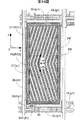
【図15】本発明による液晶表示装置の画素領域の他の実施例を示す平面図である。
【図16】第15図の16−16線における断面図である。
【図17】第15図の17−17線における断面図である。
【図18】第15図の18−18線における断面図である。
【図19】本発明による液晶表示装置の製造方法の他の実施例を示す工程図である。
【図20】本発明による液晶表示装置の製造方法の他の実施例を示す工程図で、上記第19図にて説明された工程に続く工程を説明する図である。
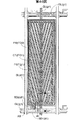
【図21】本発明による液晶表示装置の画素領域の他の実施例を示す平面図である。
【図22】第21図の22−22線における断面図である。
【図23】本発明による液晶表示装置の画素領域の他の実施例を示す平面図である。
【図24】第23図の24−24線における断面図である。
【図25】第23図の25−25線における断面図である。
【図26】第23図の26−26線における断面図である。
【図27】本発明による液晶表示装置の画素領域の他の実施例を示す平面図である。
【図28】第27図の28−28線における断面図である。
【図29】第27図の29−29線における断面図である。
【図30】第27図の30−30線における断面図である。
【図31】本発明による液晶表示装置の画素領域の他の実施例を示す平面図である。
【図32】第31図の32−32線における断面図である。
【図33】第31図の33−33線における断面図である。
【図34】第31図の34−34線における断面図である。
【図35】上述した各実施例の液晶表示装置の印加電圧−透過率の特性を示すグラフである。
【図36】本発明による液晶表示装置の画素領域の他の実施例を示す平面図である。
【図37】本発明による液晶表示装置の画素領域の他の実施例を示す平面図である。
【図38】第37図の38−38線における断面図である。
【図39】第37図の39−39線における断面図である。
【図40】本発明による液晶表示装置の画素領域の他の実施例を示す平面図である。
【図41】第40図の41−41線における断面図である。
【図42】本発明による液晶表示装置の画素領域の他の実施例を示す説明図である。
【図43】本発明による液晶表示装置の画素領域の他の実施例を示す断面図である。
【図44】本発明による液晶表示装置の画素領域の他の実施例を示す平面図である。
【図45】第44図の45−45線における断面を示す図である。
【図46】本発明による液晶表示装置の画素領域の他の実施例を示す平面図である。
【図47】第46図の47−47線における断面を示す図である。
【図48】本発明による液晶表示装置の画素領域の他の実施例を示す平面図である。
【図49】本発明による液晶表示装置の画素領域の他の実施例を示す平面図である。
【図50】本発明による液晶表示装置の画素領域の他の実施例を示す平面図である。
【0012】
【発明の実施の形態】
以下、実施例により本発明による液晶表示装置をより詳細に説明する。
【0013】
〔実施例1〕
<画素の構成>
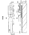
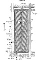
第1図は、本発明による液晶表示装置(パネル)の画素領域における構成図であり、液晶を介して互いに対向配置される各透明基板のうちの一方の透明基板の液晶側から観た平面図である。
第1図の2−2線における断面図を第2図に、3−3線における断面図を第3図に、4−4線における断面図を第4図に示している。
【0014】
まず、第1図において、図中x方向に延在されy方向に並設されるゲート信号線GLがたとえばクロム(Cr)で形成されている。このゲート信号線GLは後述するドレイン信号線DLとで矩形状の領域を形成し、その領域は画素領域を構成するようになっている。
【0015】
そして、この画素領域には、後述する画素電極PXとの間で電界を発生せしめる対向電極CTが形成され、この対向電極CTは該画素領域の周辺を除く全域に形成され、透明導電体であるたとえばITO1(Indium-Tin-Oxide)から構成されている。
【0016】
この対向電極CTは、その周辺の全域を縁取るようにして該対向電極CTと接続された対向電圧信号線CLが形成され、この対向電圧信号線CLは図中左右の画素領域(ゲート信号線GLに沿って配置される各画素領域)における対向電極CTに同様に形成された対向電圧信号線CLと一体的に形成されている。
【0017】
この場合における画素領域の対向電圧信号線CLどうしの接続は、画素領域の上部および下部のそれぞれでなされている。対向電圧信号線CLと後述のドレイン信号線DLとの重なりの部分を極力小さくし、それらの間に発生する容量を小さくする趣旨である。
【0018】
この対向電圧信号線CLは、たとえばクロム(Cr)からなる不透明の材料で形成されている。このようにした場合、後述のドレイン信号線DLとこれに近接する対向電極CTの辺部との間にノイズとして作用する電界が発生し、それによって液晶の光透過率が所望通りに得られなくても、その部分は該対向電圧信号線CLによって遮光されることから、表示品質の面からの不都合を解消できるようになる。
このことは、ゲート信号線GLとこれに近接する対向電極CTの周辺部との間に発生する電界(ノイズ)による不都合も解消できることを意味する。
【0019】
また、上述したように、対向電圧信号線CLの材料をゲート信号線GLと同一の材料とすることにより、それらを同一の工程で形成でき製造工数の増大を回避させることができる。
【0020】
ここで、前記対向電圧信号線CLは、Crに限定されることなく、たとえばAl、あるいはAlを含有する材料で形成するようにしてもよいことはいうまでもない。
【0021】
しかし、この場合、この対向電圧信号線CLは対向電極CTに対して上層に位置づけるのが効果的となる。けだし、対向電極CTを構成するITO膜の選択エッチング液(たとえばHBr)は容易にAlを溶解してしまうからである。
【0022】
さらに、対向電圧信号線CLの対向電極CTとの少なくとも接触面にはTi、Cr、Mo、Ta、W等の高融点金属を介在させることが効果的となる。けだし、対向電極CTを構成するITOは対向電圧信号線CL中のAlを酸化させて高抵抗層を生成させてしまうからである。
【0023】
このため、一実施例として、Al、あるいはAlを含有する材料からなる対向電圧信号線CLを形成する場合、前記高融点金属を一層目とする多層構造とすることが好ましい。
【0024】
そして、このように対向電極CT、対向電圧信号線CL、およびゲート信号線GLが形成された透明基板の上面には、それらをも被ってたとえばSiNからなる絶縁膜GIが形成されている。
【0025】
この絶縁膜GIは、後述のドレイン信号DLに対しては対向電圧信号線CLおよびゲート信号線GLの層間絶縁膜としての機能を、後述の薄膜トランジスタTFTの形成領域においてはそのゲート絶縁膜としての機能を、後述の容量素子Cstgの形成領域においてはその誘電体膜としての機能を有するようになっている。
【0026】
そして、ゲート信号線GLの一部(図中左下)に重畳されて薄膜トランジスタTFTが形成され、この部分の前記絶縁膜GI上にはたとえばa−Siからなる半導体層ASが形成されている。
【0027】
この半導体層ASの上面にソース電極SD1およびドレイン電極SD2が形成されることによって、ゲート信号線GLの一部をゲート電極とする逆スタガ構造のMIS型トランジスタが形成されることになる。そして、このソース電極SD1およびドレイン電極SD2はドレイン信号線DLと同時に形成されるようになっている。
【0028】
すなわち、第1図中y方向に延在されx方向に並設されたドレイン信号線DLが形成され、このドレイン信号線DLの一部が前記半導体層ASの表面にまで延在されることによって薄膜トランジスタTFTのドレイン電極SD2を構成するようになっている。
【0029】
また、該ドレイン信号線DLの形成の際にソース電極SD1が形成され、このソース電極SD1は画素領域内にまで延在されて後述の画素電極PXとの接続を図るコンタクト部をも一体的に形成されるようになっている。
【0030】
なお、第3図に示すように、半導体層ASの前記ソース電極SD1およびドレイン電極SD2との界面にはたとえばn型不純物がドーピングされたコンタクト層d0が形成されている。
【0031】
このコンタクト層d0は、半導体層ASの表面の全域にn型不純物ドーピング層を形成し、さらにソース電極SD1およびドレイン電極SD2の形成後において、該各電極をマスクとしてこれら各電極から露出された半導体層ASの表面のn型不純物ドーピング層をエッチングすることによって形成されるようになっている。
【0032】
なお、この実施例では、半導体層ASは薄膜トラジスタTFTの形成領域ばかりでなく、ドレイン信号線DLに対するゲート信号線GL、対向電圧信号線CLとの交差部にも形成されている。層間絶縁膜としての機能を強化させるためである。
【0033】
そして、このように薄膜トランジスタTFTが形成された透明基板の表面には、該薄膜トランジスタTFTをも被ってたとえばSiNからなる保護膜PSVが形成されている。薄膜トラジスタTFTの液晶LCとの直接の接触を回避するためである。
【0034】
さらに、この保護膜PSVの上面には画素電極PXがたとえばITO2(Indium-Tin-Oxide)からなる透明な導電膜によって形成されている。
【0035】
画素電極PXは、前記対向電極CTの形成領域に重畳されて、この実施例では5本形成され、それぞれ図中y方向に延在して等間隔に形成されているとともに、その両端はそれぞれx方向に延在する同材料層で互いに接続されるようになっている。
【0036】
ちなみに、この実施例では、隣り合う画素電極PX間の間隔Lはたとえば1〜15μm、幅Wはたとえば1〜10μmの範囲で設定されるようになっている。
【0037】
この場合、各画素電極PXの下端の同材料層は前記保護膜PSVに形成されたコンタクト孔を通して前記薄膜トランジスタTFTのソース電極SD1のコンタクト部と接続されるようになっており、また、上端の同材料層は前記対向電圧信号線CLと重畳されて形成されている。
【0038】
このように構成した場合、対向電極CTと各画素電極PXとの重畳部には絶縁膜GIと保護膜PSVとの積層膜を誘電体膜とする容量素子Cstgが形成されるようになっている。
【0039】
この容量素子Cstgは、薄膜トランジスタTFTを介してドレイン信号線DLからの映像信号が画素電極PXに印加された後に、該薄膜トランジスタTFTがオフとなっても該映像信号が画素電極PXに比較的長く蓄積される等のために設けられたものとなっている。
【0040】
ここで、この容量素子Cstgの容量は、対向電極CTと各画素電極PXとの重畳面積に比例し、その面積が比較的大きくなってしまって必要以上の値に設定されてしまう憂いがあるが、その誘電体膜は絶縁膜GIと保護膜PSVとの積層構造となっていることから結果的にはその憂いはない構成となっている。
【0041】
すなわち、絶縁膜GIは薄膜トランジスタTFTのゲート絶縁膜として機能させることから、その膜厚を大きくできないが、保護膜PSVに関しては、そのような制約がないことから、該保護膜PSVを前記絶縁膜GIとともに所定の膜厚(保護膜PSVのみの膜厚はたとえば100nm〜4μm)にすることによって該容量素子Cstgの容量を所定の値に低減させることができる。
【0042】
なお、前記保護膜PSVとしては、SiNに限定されることなく、たとえば合成樹脂によって形成されていてもよいことはいうまでもない。この場合、塗布により形成することから、その膜厚を大きく形成する場合においても製造が容易であるという効果を奏する。
【0043】
そして、このように画素電極PXおよび対向電極CTが形成された透明基板の表面には該画素電極PXおよび対向電極CTをも被って配向膜ORI1が形成されている。この配向膜ORI1は液晶LCと直接に接触する膜で該液晶LCの初期配向方向を決定づけるものとなっている。
【0044】
なお、上述した実施例では、画素電極PXを透明な電極として構成したものであるが、必ずしも透明でなく、たとえばCrのような不透明の金属材料であってもよい。これによって開口率が若干低下するが、液晶LCの駆動においては全く支障がないからである。
【0045】
上記実施例において、ゲート信号線GL、対向電圧信号線CL、ドレイン信号線DLについてはクロム(Cr)を用いて説明したが、他の高融点金属、Mo、W、Ti、Ta、あるいはこれらの2種以上の合金、あるいはこれらの2種以上の積層膜を用いてもよいことはもちろんである。
【0046】
さらに、透明導電膜についてもITOを用いて説明したが、IZO(Indium-Zinc-Oxide)でも同様の効果が得られることはいうまでもない。
【0047】
<フィルタ基板>
このように構成された透明基板はTFT基板と称され、このTFT基板と液晶LCを介して対向配置される透明基板はフィルタ基板と称されている。
【0048】
フィルタ基板は、第2図に示すように、その液晶側の面に、まず、各画素領域を画するようにしてブラックマトリックスBMが形成され、このブラックマトリックスBMの実質的な画素領域を決定する開口部にはそれを被ってフィルタFILが形成されるようになっている。
【0049】
そして、ブラックマトリックスBMおよびフィルタFILを被ってたとえば樹脂膜からなるオーバーコート膜OCが形成され、このオーバーコート膜の上面には配向膜ORI2が形成されている。
【0050】
<液晶表示パネルの全体構成>
第5図は、マトリックス状に配置された各画素領域の集合によって構成される表示領域ARを示す液晶表示パネルの全体構成図である。
【0051】
透明基板SUB2は、透明基板SUB1に対して若干小さく形成され、その図中右側辺および下側辺は透明基板SUB1の対応する辺とそれぞれほぼ面一となるように配置されるようなっている。
【0052】
これにより、透明基板SUB1の図中左側辺および上側辺は透明基板SUB2によって被われない領域が形成され、この領域において、それぞれ、各ゲート信号線GLに走査信号を供給するためのゲート信号端子Tg、各ドレイン信号線DLに映像信号を供給するためのドレイン信号端子Tdが形成されるようになっている。
【0053】
透明基板SUB2の透明基板SUB1に対する固定は、該透明基板SUB2の周辺に形成されたシール材SLによってなされ、このシール材SLは各透明基板SUB1、SUB2の間に液晶LCを封入するための封入材としての機能をも有している。
【0054】
第6図は、各透明基板SUB1、SUB2の間に介在される液晶LCはシール材SLよって封入されていることを示している。
【0055】
なお、このシール材SLの一部(第5図の中右側)には液晶封入口INJがあり、この液晶封入口INJは、ここから液晶を封入した後は、図示しない液晶封止剤によって封止されるようになっている。
【0056】
<ゲート信号端子>
第7図は、各ゲート信号線GLに走査信号を供給するためのゲート信号端子GTMを示した構成図で、第7図(a)は平面図、第7図(b)は同図(a)のB−B線における断面図である。
【0057】
まず、透明基板SUB1上にたとえばITO膜ITO1からなるゲート信号端子GTMが形成されている。このゲート信号端子GTMは対向電極CTと同時に形成されるようになっている。
【0058】
ゲート信号端子GTMの材料としてITO膜ITO1を用いたのは電食の発生を困難にするためである。
【0059】
そして、このゲート信号端子GTMには、そのゲート信号線GL側の端部においてゲート信号線GLが被うようにして形成されている。
【0060】
さらに、これらゲート信号端子GTMおよびゲート信号線GLを被って絶縁膜GIおよび保護膜PSVが順次積層され、これら保護膜PSVおよび絶縁膜GIに設けた開口によって、ゲート信号端子GTMの一部が露呈されるようになっている。
【0061】
なお、前記絶縁膜GIおよび保護膜PSVは、表示領域ARにおけるそれらの延在部分として形成されるものである。
【0062】
<ドイレン信号端子>
第8図は、ドレイン信号線DLに映像信号を供給するためのドレイン信号端子DTMを示した構成図で、第8図(a)は平面図、第8図(b)は同図(a)のB−B線における断面図である。
【0063】
まず、透明基板SUB1上に形成されるドレイン信号端子DTMは、電食に対して信頼性のあるITO膜ITO1から構成され、このITO膜ITO1は対向電極CTと同時に形成されるようになっている。
【0064】
そして、このドレイン信号端子DTMは、絶縁膜GI上に形成されるドレイン信号線DLと接続されることになるが、該絶縁膜GIにコンタクト孔を形成して接続させようとする場合に以下のような不都合が発生する。
【0065】
すなわち、ITO膜上に形成されたSiNからなる絶縁膜GIは、該ITO膜と接触する部分において白濁が生じ、その部分にコンタクト孔を形成した場合に該孔は逆テーパ状に形成され、ドレイン信号線DLの接続に不良が生じる可能性を残すことになる。
【0066】
このため、同図に示すように、ドレイン信号端子DTMの端部に重畳させてたとえばCrからなる金属層glを形成し、この金属層gl上の絶縁膜GIにコンタクト孔を形成するようにしている。
【0067】
そして、このコンタクト孔の形成は、該絶縁膜GIの上に保護膜PSVを形成した後に行なうことによって製造工数の低減を図っていることから、該保護膜PSVに形成したコンタクト孔を通し、画素電極PXと同時に形成されるITO膜ITO2によってドレイン信号線DLと前記金属層glとの接続を行っている。
【0068】
ここで、前記金属層glはCrを用いた場合を示したものであるが、AlあるいはAlを含む材料であってもよい。この場合、上述したようにITO膜との接触面において酸化されやすいことから、たとえば該金属層glをTi/Al/Tiというように、上下面のそれぞれに高融点金属層を設けた三層構造とすることによって良好な接続を図ることができるようになる。
【0069】
<対向電圧信号端子>
第9図は、対向電圧信号線CLに対向電圧信号を供給するための対向電圧信号端子CTMを示した構成図で、第9図(a)は平面図、第9図(b)は同図(a)のB−B線における断面図である。
【0070】
透明基板SUB1上に形成される対向電圧信号端子CTMも、電食に対して信頼性のあるITO膜ITO1から構成され、このITO膜ITO1は対向電極CTと同時に形成されるようになっている。
【0071】
そして、この対向電圧信号端子CTMには、その対向電圧信号線CL側の端部において該対向電圧信号線CLが被うようにして形成されている。
【0072】
さらに、これら信号線を被って、表示領域ARにおけるそれらの延在部分として形成される絶縁膜GIおよび保護膜PSVが順次積層され、これら保護膜PSVおよび絶縁膜GIに設けた開口によって、対向電圧信号端子CTMの一部が露呈されるようになっている。
【0073】
<等価回路>
第10図は、液晶表示パネルの等価回路を該液晶表示パネルの外付け回路とともに示した図である。
【0074】
第10図中、x方向に延在されy方向に並設される各ゲート信号線GLには垂直走査回路Vによって順次走査信号(電圧信号)が供給されるようになっている。
【0075】
走査信号が供給されたゲート信号線GLに沿って配置される各画素領域の薄膜トランジスタTFTは該走査信号によってオンするようになっている。
【0076】
そして、このタイミングにあわせて映像信号駆動回路Hから各ドレイン信号線DLに映像信号が供給されるようになっており、この映像信号は各画素領域の該薄膜トランジスタを介して画素電極PXに印加されるようになっている。
【0077】
各画素領域において、画素電極PXとともに形成されている対向電極CTには対向電圧信号線CLを介して対向電圧が印加されており、それらの間に電界を発生させるようになっている。
【0078】
そして、この電界のうち透明基板SUB1と平行な成分を有する電界(横電界)によって液晶LCの光透過率を制御するようになっている。
【0079】
なお、同図において各画素領域に示したR、G、Bの各符号は、各画素領域にそれぞれ赤色用フィルタ、緑色用フィルタ、青色用フィルタが形成されていることを示している。
【0080】
<画素表示のタイミングチャート>
第11図は、液晶表示パネルに供給する各信号のタイミングチャートを示すもので、図中、VGはゲート信号線GLに供給する走査信号を、VDはドレイン信号線DLに供給する映像信号を、また、VCは対向電圧信号線CTに供給する対向電圧信号を示している。
【0081】
対向電圧信号VCの電位を一定にした一般的なライン反転(ドッド反転)を示す駆動波形図である。
【0082】
<液晶表示パネルモジュール>
第12図は、第5図に示した液晶表示パネルに外付け回路を実装したモジュール構造を示した平面図である。
【0083】
同図において、液晶表示パネルPNLの周辺には、垂直走査回路V、映像信号駆動回路H、および電源回路基板PCB2が接続されている。
【0084】
垂直走査回路Vは、複数のフィルムキャリア方式で形成された駆動ICチップから構成され、その出力バンプは液晶表示パネルのゲート信号端子GTMに接続され、入力バンプはフレキシブル基板上の端子に接続されている。
【0085】
映像信号駆動回路Hも、同様に、複数のフィルムキャリア方式で形成された駆動ICチップから構成され、その出力バンプは液晶表示パネルのドレイン信号端子DTMに接続され、入力バンプはフレキシブル基板上の端子に接続されている。
【0086】
電源回路基板PCB2はフラットケーブルFCを介して映像信号駆動回路Hに接続され、この映像信号駆動回路HはフラットケーブルFCを介して垂直走査回路Vに接続されている。
【0087】
なお、本発明では、このようなものに限定されることはなく、各回路を構成する半導体チップを透明基板SUB1に直接搭載し、その入出力バンプのそれぞれを該透明基板SUB1に形成された端子(あるいは配線層)に接続させるいわゆるCOG(Chip On Glass)方式にも適用できることはいうまでもない。
【0088】
<製造方法>
第13図及び第14図は、上述したTFT基板の製造方法の一実施例を示す工程図である。
【0089】
この製造は(A)乃至(F)までのフォト工程を経て完成され、第13図並びに第14図の夫々において、図中左側は画素領域を、図中右側はドレイン信号端子形成領域を示している。
【0090】
以下、工程順に説明する。
工程(A)
透明基板SUB1を用意し、その表面の全域にたとえばスパッタリングによってITO膜を形成する。そして、フォトリソグラフィ技術を用いて該ITO膜を選択エッチングし、画素領域には対向電極CTを、またドレイン信号端子形成領域にはドレイン信号端子DTMを形成する。
【0091】
工程(B)
透明基板SUB1の表面の全域にCr膜を形成する。そして、フォトリソグラフィ技術を用いて該Cr膜を選択エッチングし、画素領域にはゲート信号線GLおよび対向電圧信号線CLを、またドレイン信号端子形成領域には中間接続体となる導電層g1を形成する。
【0092】
工程(C)
透明基板SUB1の表面の全域にたとえばCVD法によってSiN膜を形成し絶縁膜GIを形成する。
さらに、この絶縁膜GIの表面の全域にたとえばCVD法によってa−Si層、n型不純物がドーピングされたa−Si層を順次形成する。
そして、フォトリソグラフィ技術を用いて該a−Si層を選択エッチングし、画素領域に薄膜トランジスタTFTの半導体層ASを形成する。
【0093】
工程(D)
透明基板SUB1の表面の全域に、たとえばスパッタリング法によってCr膜を形成し、フォトリソグラフィ技術を用いて該Cr膜を選択エッチングし、画素領域にドレイン信号線DL、薄膜トランジスタTFTのソース電極SD1およびドレイン電極SD2を、またドレイン信号端子形成領域に該ドレイン信号線DLの延在部を形成する。
【0094】
工程(E)
透明基板SUB1の表面の全域に、たとえばCVD法によってSiN膜を形成し保護膜PSVを形成する。そして、フォトリソグラフィ技術を用いて該保護膜PSVを選択エッチングし、画素領域に薄膜トランジスタTFTのドレイン電極SD2の一部を露呈させるコンタクト孔を形成するとともに、ドレイン信号端子形成領域には該保護膜PSVの下層の絶縁膜GIにまで貫通させて前記導電層g1の一部を露呈させるコンタクト孔を形成する。
【0095】
工程(F)
透明基板SUB1の表面の全域にたとえばスパッタリング法によってITO膜ITO2を形成する。そして、フォトリソグラフィ技術を用いて該ITO膜を選択エッチングし、画素領域に前記コンタクト孔を通して薄膜トランジスタTFTのドレイン電極SD2と接続された画素電極PXを形成するとともに、ドレイン信号端子形成領域にはドレイン信号線DLと前記導電層g1との接続を図る接続体層を形成する。
【0096】
上記製造方法において、工程(A)と工程(B)は逆転し得る。すなわち、ゲート信号線GL上に対向電極CTを上部より接続させる構成となる。この場合、ゲート信号線GLの断面形状は緩やかなテーパ加工が必要となる。
【0097】
一方、本方式では、対向電極CTがゲート信号線GLや対向電圧信号線CLより下部にあるので、ゲート信号線GLの断面形状に拘らず良好な接続が得られることになる。
【0098】
一方、本実施例では、ゲート絶縁膜GIとしてSiN膜を用いたが、ITO上の白濁を確実に回避するために少なくともITOと接触するゲート絶縁膜GIをSiO2やSiON等の酸素を含む絶縁膜を用いてもよい。
【0099】
〔実施例2〕
<画素の構成>
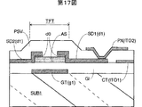
第15図は、本発明による液晶表示装置の他の実施例を示す平面図で、同図の16−16線における断面図、17−17線における断面図、18−18線における断面図を、それぞれ第16図、第17図、第18図に示している。
【0100】
実施例1に示した第1図と対応しており、それと同符号のものは同一の材料を示している
【0101】
実施例1と異なる構成は、まず、透明電極からなる対向電極CTが絶縁膜GI上に形成され、ドレイン信号線DLと同層になっている。
【0102】
このことは、対向電極CTはゲート信号線GLと異なった層として形成されていることを意味する。
【0103】
そして、該対向電極CTのドレイン信号線DLと近接する辺部に設けられる導電膜FGTは、ゲート信号線GLと同層に設けられており、該対向電極CTとは電気的に接続されていない状態で形成されている。
【0104】
このため導電膜FGTは、実施例1のように、対向電圧信号線CLの一部として機能することはなく、専ら、ドレイン信号線DLと対向電極CTとの間にノイズとして発生する電界による液晶の光漏れ等を遮光する遮光材として機能するようになっている。
【0105】
このように構成した場合、ドレイン信号線DLと対向電極CTとの間隔を狭めることができて開口率を向上させることができる効果を有する。
【0106】
しかし、該導電膜FGTはこのように形成することなく、対向電極CTと同層に形成し、該対向電極CTのドイレン信号線DLと近接する辺部に一部接続させて形成してもよいことはもちろんである。
【0107】
そして、各画素領域のうちドレイン信号線DLに沿って(ゲート信号線GLに直交する方向に)配置される各画素領域の対向電極CTは、互いに接続されて構成されている。
【0108】
すなわち、各画素領域の対向電極CTは、ゲート信号線GLが形成されている領域を股いで互いに一体的に形成されている。
【0109】
換言すれば、ドレイン信号線DLに沿って配置される各画素領域の対向電極CTは該ドレイン信号線DLに沿って帯状に形成され、これら帯状の各対向電極CTはドレイン信号線DLの形成領域によって分断されている。
【0110】
この対向電極CTはゲート信号線GLと異なる層で形成されており、このゲート信号線GLに接続されることなく形成できる。
【0111】
このように帯状に形成された対向電極CTは画素領域の集合体として形成される表示領域の外側から対向電圧信号が供給されるようにすれば、実施例1に示したような対向電圧信号線CLを特に形成せずに済むという効果を奏する。
【0112】
このため、画素電極PXは、ゲート信号線GLにより近接させて、あるいは、さらに該ゲート信号線GL上に重畳させた状態にまで延在させる(第15図参照)ことによって、該ゲート信号線GLの近傍においても画素領域としての機能をもたせることができるようになる。
【0113】
このことは、ゲート信号線GLの近傍において、該ゲート信号線GLそれ自体にブラックマトリックスとしての機能をもたせるだけで充分となり(換言すれば、ゲート信号線GLとその近傍を被うブラックマトリックスを必要としない)、開口率の大幅な向上が図れるという効果を奏する。
【0114】
なお、上述した実施例では、各画素領域のうちドレイン信号線DLに沿って配置される各画素領域の対向電極CTを共通に構成したものである。しかし、ゲート信号線GLに沿って配置される各画素領域の対向電極CTを共通に構成するようにしてもよいことはいうまでもない。
【0115】
この場合、対向電極CTはドレイン線DLと異なる層で構成されていることが必要となり、たとえば実施例1の構成において適用できる。
【0116】
<製造方法>
第19図及び第20図は上述した実施例で示した液晶表示装置の製造方法の一実施例を示した工程図であり、第13図及び第14図と対応した図となっている
【0117】
実施例1の場合と比較して、対向電極CTが絶縁膜GIの上面に形成され、この対向電極CT上に保護膜PSVを介して画素電極PXが形成されている構成の相違に対応させて、製造工程に相違を有するようになっている。
【0118】
〔実施例3〕
第21図は本発明による液晶表示装置の他の実施例を示す平面図で第15図に対応した図となっている。この第21図の22−22線における断面図を第22図に示している。
【0119】
第21図において、第15図と同一の符号は同一の材料を示している。第15図の構成と異なる部分は、まず、ドレイン信号線DLに沿って配置される各画素領域内を該ドレイン信号線DLとほぼ平行に走行する対向電圧信号線CLが形成されていることにある。
【0120】
この対向電圧信号線CLは、対向電極CTの直下に(あるいは直上であってもよい)に形成され、換言すれば該対向電極CTに接続されて形成され、対向電極CTのそれ自体の電気的抵抗を低減させる機能をもたせている。
【0121】
この対向電圧信号線CLはたとえばドレイン信号線DLと同時に形成され、該ドレイン信号線DLと同一の材料からなっている。このことから、該対向電圧信号線CLは、対向電極CTを構成するITOよりも電気的抵抗の小さな導電層から構成されている。
【0122】
そして、この対向電圧信号線CLは、画素領域をほぼ2等分するようにしてその中央を走行するようになっている。その両脇に存在するドレイン信号線DLとの短絡を確実に回避できるように形成できるからである。
【0123】
さらに、この対向電圧信号線CLは、図中y方向に延在して形成される画素電極PXのうちの一つと重畳されて形成されている。
【0124】
画素電極PXの形成されている部分は光透過率の低減が免れない部分となっていることから、この部分に対向電圧信号線CLを位置づけさせることによって、画素領域の全体における光透過率の低減を最小限に抑えようとする趣旨である。
【0125】
この実施例では、ドレイン信号線DLの上面にITO膜ITO1が積層されて形成され、該ドレイン信号線DLが断線されて形成された場合でも該ITO膜ITO1によって該断線を修復できる構成となっている。
【0126】
このITO膜ITO1は、対向電極CTの形成の際に同時に形成できるので、製造工数の増大を回避できる効果を奏する。
【0127】
〔実施例4〕
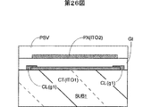
第23図は、本発明による液晶表示装置の他の実施例を示す平面図で、その24−24線における断面図、25−25線における断面図、26−26線における断面図を、それぞれ第24図、第25図、第26図に示している。
【0128】
第23図は第1図に対応した図となっており、同一の符号は同一の材料を示している。
第23図において、第1図と異なる構成は、画素電極PXが絶縁膜GI上に形成され、対向電極CTとはこの絶縁膜GIを介して配置されている。すなわち、液晶側の画素電極PXは保護膜PVS(および配向膜ORI1)を介して配置されている。
【0129】
このようにした場合、液晶LC中への電気力線が保護膜PVSによる分圧効果によって増大され、該液晶LCの材料として低抵抗のものを選択でき、結果として残像の少ない表示を得る効果を奏する。
【0130】
また、このようにした場合、第25図に示すように、薄膜トランジスタTFTのソース電極SD1と画素電極PXとの接続を直接行なうことができるので、たとえば保護膜等に形成したコンタクト孔を通して行なう煩雑さを解消することができる。
【0131】
〔実施例5〕
第27図は、本発明による液晶表示装置の他の実施例を示す平面図で、その28−28線における断面図、29−29線における断面図、30−30線における断面図を、それぞれ第28図、第29図、第30図に示している。
【0132】
第27図は第1図に対応した図となっており、同一の符号は同一の材料を示している。
第27図において、第1図と異なる構成は、まず、絶縁層を介して画素電極PXは下層に位置づけられ、対向電極CTは上層に位置づけられている。
【0133】
第28図に示すように、絶縁膜GIの上面に第1保護膜PSV1が形成され、この第1保護膜PSV1上に画素電極PXが形成されている。
【0134】
この画素電極PXは画素領域の周辺を除く大部分の領域に形成された透明からなる電極で、第1保護膜PSV1の下層に形成される薄膜トランジスタTFTのソース電極SD2とコンタクト孔を通して接続されている。
【0135】
そして、このように形成された画素電極PXをも被って第2保護膜PSV2が形成され、この第2保護膜PSV2の上面に対向電極CTが形成されている。
【0136】
この対向電極CTは、前記画素電極PXに重畳される領域に図中y方向に延在しx方向に並設される複数の帯状の電極として形成されるが、それらの両端部は各対向電極CTの間の領域を除く他の全ての領域に該各対向電極CTと一体的に形成された導電層と接続されて形成されている。
【0137】
換言すれば、対向電極CTは、少なくとも表示領域を被うようにして形成された導電層(ITO)のうち、前記画素電極PXに重畳される領域内の導電層に、図中y方向に延在しx方向に並設される複数の帯状の開口を形成することによって、形成されるようになっている。
【0138】
このことは、対向電極CTとして機能する導電層以外の他の導電層は対向電圧信号線CLとして利用でき、このようにした場合、導電層全体の電気抵抗を大幅に低減できるという効果を奏するようになる。
【0139】
また、対向電極CTとして機能する導電層以外の他の導電層は、ゲート信号線GLおよびドレイン信号線DLを被った状態で形成できることになる。
【0140】
このことは、対向電極CTとして機能する導電層以外の他の導電層は従来のブラックマトリックス層としての機能をもたせることができることを意味する。
【0141】
液晶の光透過率を制御する透明基板と平行な成分をもつ電界(横電界)は、対向電極CTとして機能する導電層と画素電極PXの間において発生し、それ以外の部分では発生し得ないからである。
【0142】
このため、第28図に示すように、透明基板SUB2側にはブラックマトリックス層を形成する必要がなくなり、製造の工数の低減が図れるという効果を奏するようになる。
【0143】
なお、この場合、液晶として、電界が印加されない状態で黒表示ができるいわゆるノーマリブラックのものを用いることによって、前記導電層のブラックマトリックスとしての機能を強化することができるようになる。
【0144】
また、ゲート信号線GLあるいはドレイン信号線DLは、前記導電膜との間で容量を発生せしめることは否めなくなる。このことから、それらの間に介在される第1保護膜PSV1および第2保護膜PSV2のうちたとえば第2保護膜PSV2を塗布で形成できる樹脂膜で構成し、この樹脂膜の膜厚を比較的大きく形成することによって該容量を小さくすることができる。
【0145】
たとえば、第1保護膜PSV1として、その比誘電率が7で、膜厚が100〜900nmのSiN膜を用いた場合、第2保護膜PSV2として、その比誘電率が3〜4で、膜厚が1000〜3000nmの有機膜が適当となる。
【0146】
また、第2保護膜PSV2は第1保護膜PSV1と比べて比誘電率が1/2以下であれば、その膜厚に関係なく、また、膜厚が2倍以上であれば、その比誘電率に関係なく、実際の製品に支障がないことが確認されている。
【0147】
〔実施例6〕
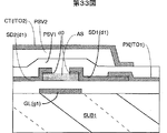
第31図は本発明による液晶表示装置の他の実施例を示す平面図であり、その32−32線における断面図を第32図に示している。
【0148】
第31図は実施例5と比較してさらに改良された構成を示すもので、第27図乃至第30図と同符号のものは同一材料を示している。
【0149】
実施例5の場合と異なる構成は、まず、画素電極PXは絶縁膜GI上に形成され、対向電極CTは該画素電極PX上に形成された第1保護膜PSV1上に形成されている。換言すれば、画素電極PXと対向電極CTは第1保護膜PSV1を介して層を異ならしめている。
【0150】
一方、画素領域を除く他の領域には第2保護膜PSV2が形成されている。この第2保護膜PSV2は、たとえば少なくとも表示領域の全域に該第2保護膜PSV2を形成した後に、画素領域に相当する部分を選択エッチングすることによって形成される。
【0151】
さらに、残存された第2保護膜PSV2の表面には導電層が形成されている。この導電層は対向電極CTと一体に形成され、実施例5の場合と同様に、少なくとも表示領域の全域に導電層を形成した後に、画素電極PXに重畳される領域内の導電層に、図中y方向に延在しx方向に並設される複数の帯状の開口を形成することによって対向電極CTが形成されるようになっている。
【0152】
このように構成された液晶表示装置は、ゲート信号線GLあるいはドレイン信号線DLと前記導電層との間に第1保護膜PSV1および第2保護膜PSV2を介在させることによってそれらの間に発生させる容量を小さくできるとともに、画素電極PXと対向電極CTとの間に第1保護膜PSV1のみを介在させることによってそれらの間の電界を液晶LC側へ強く発生させることができる効果を奏する。
【0153】
〔上記各実施例の特性比較〕
第35図は、上記実施例1、実施例2、実施例4、実施例5、および実施例6の各構成における印加電圧に対する透過率の特性を示したグラフを示している。
【0154】
ここで、各実施例の液晶表示装置は、いわゆる15形XGA規定のもので、ゲート信号線GLの幅を10μm、ドイレン信号線DLの幅を8μmとしたものを対象としている。
【0155】
第35図では、比較のため、上記各実施例の他に、TN型のTFT−LCDおよびIPS型のTFT−LCDの特性をも示している。
【0156】
第35図から、実施例1においてはその開口率が60%、実施例2においてはその開口率が70%、実施例4においてはその開口率が50%、実施例5および6においてはその開口率が80%になることが確認される。
【0157】
ここで、実施例5および6の場合に開口率が特に高いのは従来用いられていたブラックマトリックスを不要とした構成としたことによる。
【0158】
また、実施例6の場合、実施例5と比較して駆動電圧を低くできるのは、画素領域において第2保護膜PSV2が形成されていない構成となっていることによる。
【0159】
上記特性は主に負の誘電異方性を有する液晶材料を用いて作成した素子の特性である。一方、正の誘電異方性を有する液晶材料を用いた場合、各実施例の透過率の最大値がそれぞれ0.5%低下したが、逆に、しきい値電圧が0.5V低下する効果が得られた。
【0160】
〔実施例7〕
第36図は、本発明による液晶表示装置の他の実施例を示した平面図で、上述した各実施例をいわゆるマルチドメンイン方式の液晶表示装置に適用した場合を示したものである。
【0161】
ここで、マルチドメイン方式とは、液晶の広がり方向に発生する電界(横電界)において、各画素領域内に該横電界の方向が異なる領域を形成するようにし、各領域の液晶の分子の捩じれ方向を逆にすることにより、たとえば表示領域を左右からそれぞれ観た場合に生じる着色差を相殺させる効果を奏するようになる。
【0162】
第36図は、例えば第1図に対応した図となっており、一方向に延在しそれと交差する方向に並設させた帯状の各画素電極PXを、前記一方向に対して角度θ(P型液晶で、配向膜のラビング方向をドレイン信号線の方向と一致づけた場合、5〜40°が適当)に傾けて延在された後に角度(−2θ)に屈曲させて延在させることを繰り返してジグザグ状に形成したものとなっている。
【0163】
この場合、対向電極CTは画素領域の周辺を除く領域に形成され、この対向電極CTに上述した構成の各画素電極PXが重畳するように配置させるだけで、マルチドメイン方式の効果を奏することができる。
【0164】
特に、画素電極PXの屈曲部において対向電極CTとの間に発生する電界は、画素電極PXの他の部分において対向電極CTとの間に発生する電界と全く異なることなく発生することが確かめられている。従来はいわゆるディスクリネーション領域と称され、液晶の分子の捩じれの方向がランダムになって不透過部が発生していた。
【0165】
このため、画素電極PXの屈曲部の近傍において光透過率の低下というような不都合が生じないという効果を奏する。
【0166】
なお、この実施例では、画素電極PXは第36図中y方向に延在させて形成したものであるが、図中x方向に延在させるようにし、それに屈曲部を設けてマルチドメイン方式の効果を得るようにしてもよい。
【0167】
また、この実施例では、画素電極PXに屈曲部を設けてマルチドメイン方式の効果を得るようにしたものである。
【0168】
しかし、画素電極PXを少なくとも画素領域の周辺を除く全域に形成し、例えば第28図に示したように、対向電極CTを一方向に延在させその方向に交差する方向に並設させた構成のものにあっては、該対向電極に屈曲部を設けてマルチドメイン方式の効果を得るようにしてもよいことはいうまでもない。
【0169】
〔実施例8〕
第37図は、本発明による液晶表示装置の他の実施例を示す平面図で、第27図と対応した図となっている。
なお、第37図中、38−38線における断面図、39−39線における断面図を、それぞれ第38図及び第39図に示している。
【0170】
第27図と同符号のものは同一の材料から構成されている。第27図との構成上の相違は、画素電極PXにある。
【0171】
この画素電極PXは、対向電極CTと重畳される部分においてその周辺を除く部分に開口が形成されて構成されている。このため、一方向に延在する対向電極CTの中心軸は前記画素電極PXの開口の中心軸とほぼ一致づけられ、該対向電極CTの幅をWとした場合、前記開口の幅はそれよりも小さいLLとして形成されている。
【0172】
このように構成した場合、該画素電極PXと対向電極CTとの間に発生する電界の分布は第27図におけるそれ全く同様にして発生できるようになっている。
【0173】
そして、前記開口を設けることによって、その分だけ画素電極PXと対向電極CTとの間の容量を小さくすることができる効果を奏する。
【0174】
上述したように、画素電極PXと対向電極CTとの間の容量は、画素電極PXに供給される映像信号を比較的長く蓄積させるためにある程度は必要となるが、必要以上に大きくなることによって、信号の遅延による表示の輝度ばらつきが発生することから、前記開口を適当な大きさにすることによって該容量を最適な値とすることができるようになる。
【0175】
ここで、前記画素電極PXに形成する開口によって該画素電極PXと対向電極CTとの間に発生する容量の値を設定しようとする場合、該画素電極PXに対する対向電極CTの位置ずれによって、所定の容量値が得られないことが考えられる。
【0176】
この場合、例えば第42図に示すように、画素電極PXの開口における一対の辺部(この図では位置ずれの不都合の顕著さを考え、図中y方向に平行な辺を例にとっている)をたとえばジグザク状に形成し、各辺のぞれぞれに山部(凸部)および谷部(凹部)が形成される開口を形成する。
【0177】
画素電極PXと対向電極CTとが、第42図(a)に示すように位置づれなく配置された場合、それらの容量の値は、それらの重畳された面積で決定されることになる。
【0178】
そして、画素電極PXに対して対向電極CTが、第42図(b)に示すようにx方向に位置づれが生じた場合にも、それらの重畳される面積が不変であり、容量の値に変化が生じない。
一方の辺の山部が引っ込んだ場合に他方の辺の山部が突き出す関係が生じるからである。
【0179】
このことから、開口のパターンは上述したものに限定されることはなく、たとえば一方の電極の位置づれに対して、該位置づれの方向に交差する開口辺の一方の辺に該電極側へ突き出す凸部が形成され、また他方の辺に該電極に対して引っ込む凸部が形成されていればよい。
【0180】
なお、このような構成は、第27図の構成を前提とするものではなく、上述した各実施例の全てに適用できるものである。例えば、対向電極CTが少なくとも画素領域の周辺を除く全域に形成されている構成となっている場合、この対向電極CTにおいて、画素電極PXと重畳される部分においてその周辺を除く部分に開口を形成するようにしてもよい。さらに、この場合の一方の電極の開口は、その周辺において他方の電極と重畳するようになっているが、必ずしも重畳されていなくてもよいことはいうまでもない。
【0181】
〔実施例9〕
第40図は、本発明による液晶表示装置の他の実施例を示す平面図で、その41−41線における断面図を第41図に示している。
【0182】
第40図及び第41図は、実施例5(図27〜図30)の改良として説明した図で、その特徴点はたとえば合成樹脂膜で構成される第2保護膜PSV2にスペーサとしての機能ももたせるようにしたものである。
【0183】
ここで、スペーサは、一方の透明基板側に対して他方の透明基板を精度よいギャップを保持して支持するもので、表示領域の全域に及んで液晶の層厚を均一にさせることが要求される。
【0184】
この実施例では、たとえばゲート信号線GLの一部に重畳する領域に該スペーサの形成領域を設け、このスペーサは第2保護膜PSV2と一体に形成された突起部として構成されている。
【0185】
このスペーサを設ける個所は各画素領域において同一の場所とすることによって、表示領域の全域に及んで液晶の層厚を均一にすることができる。同一の場所であれば、そこの部分の積層構造が同一であるからである。
【0186】
このスペーサは、たとえば第2保護膜PSV2を形成する際に、まず、光感光性の合成樹脂膜をスペーサの高さ分を加算させた膜厚で形成し、その後、たとえばスペーサの形成領域に強い光を、そしてスペーサの形成領域外の領域に弱い光を選択的に照射させ、現像工程を経ることによって形成できるようになる。
【0187】
このように形成される各スペーサは、同じ高さのものが精度よく得られるようになることから、各透明基板の間のギャップを表示領域の全域にわたって均一に保持させることができるようになる。
【0188】
なお、この実施例では、スペーサの形成後において、対向電極を形成する必要があるが、たとえ、スペーサの頂面において該対向電極の材料が残存したとしても、いわゆるフィルタ基板の側には電極が配置されていない構成となっていることから、それによる不都合は生じないようになっている。
【0189】
また、この実施例では、実施例5の改良として説明したものであるが、この実施例に限定されることはないことはいうまでもない。
【0190】
液晶に近い層として合成樹脂膜を形成する必要のある場合には、それと一体にスペーサを形成できる効果を有するが、そうでない場合であっても、いずれか一方の透明基板に固定されたスペーサを形成することは、各透明基板の間のギャップを精度よく均一にできるからである。
【0191】
〔実施例10〕
第43図は本発明による液晶表示装置の他の実施例を示す断面図である。 第43図は実施例5と比較してさらに改良された構成を示すもので、第27図の28−28線に沿った別の断面図を示している。なお、画素領域を示す平面図は実施例5の第27図と同一構成となる。
【0192】
実施例1との構成上の相違は、まず、対向電極CTの下部であり、画素電極PXを絶縁分離している保護絶縁膜PSV2が対向電極CTあるいは対向電圧信号配線CLをマスクとして掘るように加工されている。
【0193】
この加工により、ドレイン信号線DLと対向電圧信号配線CLの間の絶縁膜PSV2は厚く、同様に、対向電極CTと画素電極PXと直接重なる領域の絶縁膜は厚く形成され、対向電極CT間の間隔部分の絶縁膜PSV2は薄く形成される。
【0194】
上記加工の効果は、厚く形成された絶縁膜は、薄膜トランジスタTFTの負荷の容量を低減させる、あるいはドレイン信号線DLの負荷容量を低減せしめる。
【0195】
一方、薄く形成された絶縁膜PSV2は画素電極PXと対向電極CT間の絶縁膜による電圧降下を低減し、液晶に充分な電圧を印加することが可能となり、液晶のしきい電圧を低減できる。
【0196】
また、上記絶縁膜PSV2の加工は対向電極CTをマスクとして加工するので、この対向電圧CTと自己整合的に加工され、表示むらが極めて発生しにくい。
【0197】
以上、実施例1乃至10を参照して説明したことから明らかなように、本発明による液晶表示装置によれば、極めて性能の高いものが得られるようになる。
【0198】
〔実施例11〕
第44図は本発明による液晶表示装置の他の実施例での画素領域における構成図であり、液晶を介して互いに対向配置される一対の透明基板の一方の透明基板を液晶側から観た平面図である。また、第45図は第44図の45−45線における断面を示した図である。
【0199】
まず、第44図において、透明基板SUB1上に図中x方向に延在されy方向に並設されるゲート信号線GLがたとえばクロム(Cr)で形成されている。このゲート信号線GLは後述するドレイン信号線DLとで矩形状の領域を形成し、その領域は画素領域を構成するようになっている。
【0200】
この画素領域には、ゲート信号線GLとともに、前記ゲート信号線GLとの接続および前記ドレイン信号線DL(後の工程で形成される)との重畳が回避されるようにして、対向電圧信号線CLが形成されている。対向電圧信号線CLは、ゲート信号線GLと同一の材料で形成してよいため、ゲート信号線GLと同一の工程で設けられる。第44図に示されるように、この対向電圧信号線CLは、画素領域の中央において図中y方向に走行する帯状の導電層CL’と、この導電層に接続されて画素領域の周辺に沿って形成された枠体状の導電層CL”とから構成され、この画素領域を間にした左右の画素領域における対向電圧信号線CLとは図中x方向に延在する対向電圧信号線CLによって互いに接続されるようになっている。この対向電圧信号線CLは、後述する対向電極CTに対向電圧信号を供給するための信号線として機能するが、遮光膜としての機能をも有するようにして形成されている。この遮光膜としての機能の詳細については後述する
【0201】
さらに、該画素領域には、その僅かな周辺部を除く中央部の全域に、透明導電体であるたとえばITO1(Indium-Tin-Oxide)からなる対向電極CTが形成されている。本実施例並びに後述の実施例12〜15においては、基板主面側に設けられる透明導電体からなる対向電極CT(ITO1)の輪郭を太線で示す。この対向電極CT(ITO1)は、これより基板主面から離れた他の透明導電体の膜(画素電極PX(ITO2)に少なくとも一部が覆われる。透明導電体としては、本実施例にて用いたITOに代えて、例えば、IZO(Indium-Zinc-Oxide)やイオン・コーティングなどで得られる金属の薄膜等、これに入射する光を十分な強度で出射できるように形成された導電膜(例えば、入射光の少なくとも60%を透過させ得る)を用いてもよい。
【0202】
この対向電極CTはその周辺部が前記対向電圧信号線CLの枠体状の導電層の内側の周辺部に直接に重畳するように形成され、これにより該対向電極CTに対向電圧信号線CLから供給される対向電圧が印加されるようになっている。これらのゲート信号線GL、対向電圧信号線CL、および対向電極CTをも被って透明基板SUB1の上面の全域には、たとえばSiNからなる絶縁膜GIが形成されている。この絶縁膜GIは、後述のドレイン信号線DLに対しては対向電圧信号線CLおよびゲート信号線GLの層間絶縁膜としての機能を、後述の薄膜トランジスタTFTの形成領域においてはそのゲート絶縁膜としての機能、後述の容量素子Cstgの形成領域においてはその誘電体膜としての機能を有するようになっている。
【0203】
第44図の左下に示されるように、ゲート信号線GLの一部に重畳される薄膜トランジスタTFTの部分の前記絶縁膜GI上には、例えばa−Siからなる半導体層ASが形成されている。
【0204】
この半導体層ASの上面にソース電極SD2およびドレイン電極SD1が形成されることによって、ゲート信号線GLの一部をゲート電極とする逆スタガ構造のMIS型トランジスタが形成されることになる。そして、このソース電極SD2およびドレイン電極SD1はドレイン信号線DLと同時に形成されるようになっている。
【0205】
すなわち、第44図においてy方向に延在されx方向に並設されたドレイン信号線DLが形成され、このドレイン信号線DLの一部が前記半導体層ASの表面にまで延在されることによって薄膜トランジスタTFTのドレイン電極SD1を構成するようになっている。
【0206】
また、該ドレイン信号線DLの形成の際にソース電極SD2が形成され、このソース電極SD2は画素領域内の一部にまで延在されて後述の画素電極PXとの接続を図るコンタクト部をも一体的に形成されるようになっている。
【0207】
なお、半導体層ASの前記ソース電極SD2およびドイレン電極SD1との界面にはたとえばn型不純物がドーピングされたコンタクト層d0が形成されている。
【0208】
このコンタクト層d0は、半導体層ASの表面の全域にn型不純物ドーピング層を形成し、さらにソース電極SD2およびドレイン電極SD1の形成後において、該各電極をマスクとしてこれら各電極から露出された半導体層ASの表面のn型不純物ドーピング層をエッチングすることによって形成されるようになっている。
【0209】
なお、この実施例では、半導体層ASは薄膜トランジスタTFTの形成領域ばかりでなく、ドレイン信号線DLに対するゲート信号線GL、対向電圧信号線CLとの交差部にも形成されている。層間絶縁膜としての機能を強化せしめためである。
【0210】
そして、このように薄膜トランジスタTFTが形成された透明基板SUB1の表面には、該薄膜トランジスタTFTをも被ってたとえばSiNからなる保護膜PSVが形成されている。薄膜トランジスタTFTの液晶LCとの直接の接触を回避するためである。
【0211】
さらに、この保護膜PSVの上面には画素電極PXがたとえばITO2(Indium-Tin-Oxide)からなる透明な導電膜によって形成されている。
【0212】
そして、この画素電極PXはその一部において、前記保護膜PSVに形成されたコンタクト孔を通して前記薄膜トランジスタTFTのソース電極SD2の延在部と接続されるようになっている。
【0213】
この画素電極PXは、画素領域のほぼ中央において第44図中y方向に延在する対向電圧信号線CL’上で屈曲部を有する複数の第1の電極PX’と、これら第1の電極PX’の各端部をそれぞれ接続する枠体状の第2の電極PX”とから構成されている。換言すれば、第1の電極PX’は、前記対向電極信号線CL’によって画される一方の画素領域側において、該対向電極信号線CL’に対して(−θ:θ<45°)の傾きを有して図中y方向に等間隔に配置され、また、他方の画素領域側において、該対向電極信号線に対して(+θ:θ<45°)の傾きを有して第44図中y方向に等間隔に配置されているとともに、各画素領域の対応する電極どうしは該対向電極信号線CL’上で互いに接続された構成となっている。
【0214】
このように第1の電極CL’に屈曲部を設けているのはいわゆるマルチドメイン方式を採用するものであり、一方の傾き(−θ)を有する画素電極と他方の傾き(+θ)を有する画素電極のそれぞれの対向電極CTに対して発生する電界の方向を異ならしめ、液晶分子の捻じれ方向を逆にすることにより、たとえば表示領域を左右からそれぞれ観た場合に生じる着色差を相殺させる効果を奏するためである。
【0215】
この第1の電極PX’の各々の屈曲部は、上述した対向電圧信号線CLのうち、画素領域の中央においてy方向に延在する信号線CL’に重畳するようにして位置づけられている。
【0216】
第1の電極PX’の屈曲部の近傍は、この部分において電界の方向がランダムとなり、厳密な横電界がかからない不透過領域(以下、この領域をディスクリネーション領域と称する)が発生することから、この領域を該信号線CL’によって遮光する構成としたものである。
【0217】
また、前記第1の電極PX’は、その屈曲部を中心として電極の広がり角は2θ(<90°)であり、鋭角となっている。
【0218】
このようにした場合、この屈曲部において対向電極CTとの間に比較的強い電界がかかり易くなり、液晶分子の回転を高速に行わしめることができるようになる。このため、この屈曲部を起点として、その周りひいては画素領域の全域に及んで液晶分子の回転の高速化を波及せしめることができ、結果としてレスポンスの高速化を図った表示を達成せしめる効果を奏するようにできる。
【0219】
また、画素電極PXのうち第2の電極PX”は、前記対向電圧信号線CLのうち枠体状に形成された信号線CL”の内側の周辺部に重畳された枠体状の電極PX”からなり、前記第1の電極PX’の延在端と接続された構成となっている。
【0220】
第2の電極PX”のうち第44図中y方向に延在する部分と、それに隣接して配置されるドレイン信号線DLとの間には、上述した対向電圧信号線CL”が図中y方向に延在されて形成されている。
【0221】
この対向電圧信号線CL”は、ドレイン信号線DLとの間の隙間をなるべく小さくするようにして、その幅が大きく形成されている。
【0222】
換言すれば、画素電極PXのうち第44図中y方向に延在する電極PX”と、それに隣接して配置されるドレイン信号線DLとの間の隙間は該対向電圧信号線CL”によって遮光されている構成となっている。
【0223】
ドレイン信号線DLからはそれに供給される映像信号によって電界が発生し、この電界は対向電圧信号線CL”側へ終端させるようにするともに、該電界によって変化する液晶の光透過率の変化による光透過を遮光させんとする趣旨である。
【0224】
このように構成された画素電極PXは、次のような種々の効果を奏するようになっている。
【0225】
まず、対向電極CTとの間で発生する電界の方向を異ならしめる領域は、画素領域を二分割して形成しているため、各画素電極PX(第1の電極PX’)の屈曲部はそれぞれ一つとなり、その総数は該第1の電極PX’の数に相当することになる。
【0226】
従来、例えば、第44図中y方向に延在されx方向に並設された各画素電極のそれぞれを、その長手方向に沿って右側へ傾斜させた後に左側へ傾斜させ、さらに右側へ傾斜させることを繰り返した、いわゆるジグザグ形状にしたもの比べ、該電極の屈曲部を大幅に減少させた構成とすることができるようになる。
【0227】
このため、該電極PX’の屈曲部において、ディスクリネーション領域が発生するのを大幅に減少させることができるようになる。
【0228】
また、画素電極PXを、前記第1の電極PX’の他に、画素領域の周辺に枠体状に配置される第2の電極PX”を新たに設けることにより、この第2の電極PX”と対向電極CTとの間にも横電界が発生するようになる。
【0229】
従来、上述したようなジグザク形状の画素電極では、隣接するドレイン信号線との間に小さなスペースと大きなスペースとが交互に形成され、このうち大きなスペースにおいては充分な横電界が発生しないいわゆるデッドスペースが生じていた。
【0230】
このため、本実施例のように構成することにより、上述したデッドスペースの発生を抑制でき、実質的な画素領域の拡大を図ることができるようになる。
【0231】
なお、この第2の電極PX”は、薄膜トランジスタTFTのソース電極SD2を介して第1の電極PX’のそれぞれに映像信号を供給させる機能をも有する。
【0232】
このため、この機能を充足する限り、第2の電極PX”は必ずしも画素領域の周辺に沿った枠体状の形状に形成する必要がないことはいうまでもない。
【0233】
たとえば、第44図の第2の電極PX”において、図中x方向に平行に位置づけられるものうち、図中上側(薄膜トランジスタTFTと反対側)のものを特に形成しなくても充分な効果が得られるようになる。このように画素電極PXが形成された透明基板SUB1の表面には該画素電極PXをも被って配向膜(第44図及び第45図には図示せず、実施例1参照)が形成されている。この配向膜は、図中y方向にラビング処理がなされた液晶LCと直接に接触する膜で、該液晶LCの初期配向方向を決定づけるものとなっている。
【0234】
なお、上述した実施例では、画素電極PXを透明な電極として構成したものであるが、必ずしも透明でなければならないことはなく、例えばCrのような不透明の金属材料であってもよい。これによって開口率が若干低下するが、液晶LCの駆動においては全く支障がないからである。
【0235】
また、このように構成された透明基板SUB1はいわゆるTFT基板と称され、このTFT基板と液晶LCを介して対向配置される透明基板はフィルタ基板と称されている。フィルタ基板は、その液晶側の面に、まず、各画素領域を画するようにしてブラックマトリックスが形成され、このブラックマトリックスの実質的な画素領域を決定する開口部にはそれを被ってフィルタが形成されるようになっている。そして、ブラックマトリックスおよびフィルタを被って、例えば樹脂膜からなるオーバーコート膜が形成され、このオーバーコート膜の上面には配向膜が形成されている。これらの詳細は、実施例1にて述べたとおりである。
【0236】
〔実施例12〕
第46図は、本発明による液晶表示装置の他の実施例を示す図で、図1に対応した図面となっている。また、第47図は第46図の47−47線における断面を示す図である。
【0237】
第44図と異なる構成は、まず、屈曲部を有する画素電極PXの該屈曲部の近傍を遮光する部材として、ドレイン信号線GLとともに形成される(したがって該信号線と材料が同一)導電層CLを用いていることにある。
【0238】
この導電層CLは対向電圧信号線LCを構成するものであり、このため、透明電極を構成される対向電極CTは、この対向電圧信号線LCCLの上層(下層であってもよい)に重畳されて形成されるようになっている。
【0239】
また、該導電層GL’CLは、画素領域のほぼ中央をy方向に走行して形成されているため、その両脇に位置づけられる各ドレイン信号線GLDLとのショートの憂いなく形成することができるようになる。
【0240】
〔実施例13〕
第48図は、本発明による液晶表示装置の他の実施例を示す図で、第44図に対応した図となっている。
【0241】
第44図との構成上の相違は画素電極PXに見られ、屈曲部を有する複数の第1の電極PX’の各端部をそれぞれ接続する枠体状の第2の電極PX”の図中y方向に延伸する部分に代えて、当該画素電極の中央部を図中y方向に延伸する第3の電極PX3を設けている。
【0242】
このように構成した場合にも、画素領域の全域にわたって画素電極をデッドスペースなく形成することができるようになる。
【0243】
〔実施例14〕
第49図は、本発明による液晶表示装置の他の実施例を示す図で、第44図に対応した図となっている。
【0244】
第44図と異なる構成は、画素領域において電界の方向が異なる領域をこの図中x方向に平行な境界によって二分割したことにある。
【0245】
このため、屈曲部を有する画素電極PX(第1の電極PX’)は、一方の画素領域において図中x方向に対して(−φ:φ>45°)の角度を有して配置され、他方の画素領域において(+φ:φ>45°)の角度を有して配置されるとともに、該境界部において対応する画素電極が互いに接続されたパターンを有している。
【0246】
このようにした場合においても、デッドスペースの縮小化、および画素電極の第1の電極PX’の屈曲部の数の減少化を図ることができるようになる。
【0247】
また、このようにした場合、配向膜の初期配向方向(図中y方向)と各電界の方向との最も好ましい設定から、第1の電極はその屈曲部における開き角度(2φ)は鈍角となるように設定できるようになる。
【0248】
このため、画素電極(第1の電極)の屈曲部におけるいわゆるディスクリネーション領域の発生の減少化を図ることができるようになる。
【0249】
このことから、この実施例の場合、各画素電極の屈曲部における遮光手段を備えた構成とはなっていないが、ディスクリネーション領域の完全なる発生の防止のため該遮光手段を設けるようにしてもよいことはいうまでもない。
【0250】
なお、第49図中、その第2の電極PX”において、図中x方向に平行に位置づけられるものうち、図中上側(薄膜トランジスタTFTと反対側)のものを特に形成しなくても充分な効果が得られることはいうまでもない。
【0251】
〔実施例15〕
第50図は、本発明による液晶表示装置の他の実施例を示す図で、第44図に対応した図となっている。
【0252】
第44図との構成上の相違は、対向電圧信号線CLと対向電極CTとの接続にある。本実施例では、ゲート信号線GLにクロム(Cr)系の合金を用い、基板上にゲート信号線GLのパターンを形成した後、SiNx等からなるゲート絶縁膜GIの成膜の前に対向電極CT(ITO1)を形成する。例えば、第13図において、(B)の工程が(A)の工程より前となる((A)工程と(B)工程との順序が逆転する)。対向電極CTをなすITO膜は、ブラックマトリクスBMの開口(その輪郭を破線で図示)により規定される画素の中心にて、対向電圧信号線CLをなすCr膜と直に接触する。
【0253】
第50図には、液晶層の光透過率を変調するために液晶分子を回転駆動させる電場の印加方向、ドレイン信号線(映像信号線、データ線とも呼ぶ)から上記画素(破線BMの枠に囲まれた領域)に洩れる電場の方向、及び図示された電極構造を覆う配向膜(図示せず)をラビング処理するときのラビングローラの進行方向(所謂ラビング方向)が夫々太線の矢印で示されている。
【0254】
本実施例では、液晶分子を回転駆動する電場は、図の上下方向(ドレイン信号線DLの延伸方向)に沿って印加される。このため、ドレイン信号線から図の左右方向に画素へ漏洩する電場(電気力線)が液晶分子の回転駆動に与える影響が低減され、縦スメア(Smear)による画質の劣化が抑えられる。液晶分子を回転駆動させる電場の方向(「液晶への電場印加方向」の矢印)とドレイン信号線DLから画素に漏洩する電場の方向(「ドレイン線からの電場方向」を示す矢印)とが交差する角度が大きいほど、上述の縦スメアの発生は抑えられる。この交差角度が小さい場合、ドレイン信号線DLと画素との間に、対向電極CT又は画素電極PXをドレイン信号線DLに沿って設けることにより、ドレイン信号線DLから画素への漏洩電場を遮蔽する必要がある。しかし、本実施例では、櫛歯状に並ぶ画素電極PX(ITO2)をドレイン線と十分な大きさの角度を以って交差するように配置したため、この遮蔽構造が不要となる。この特徴は、第50図に示す画素の左上及び右下にみられ、画素自体の開口率(液晶分子の回転駆動により変調される光を透過できる面積)を大きくする。
【0255】
また、本実施例によれば、基板主面からみて一方の透明導電体の膜ITO1より離れて形成された他方の透明導電体の膜ITO2(その断面構造から見て、上部ITO層ともよぶ)により構成される電極構造の設計自由度が高くなる。このため、ドレイン信号線DLの延伸方向に交差する(望ましくは略直交する)方向に沿ってこれから供給される電圧信号を画素電極PXに印加するように画素全体を設計することができる。
【0256】
なお、本実施例においては、ドレイン信号線DLに対して画素電極PXの櫛歯の延伸方向が直交していないため、ラビング方向(これに沿った方向に、電場が印加されない状態での液晶分子が配向する)をドレイン信号線に対して直交する方向に設定することができる。
【0257】
上述した実施例11乃至14では、対向電極CTは画素領域の僅かな周辺を除く中央部の全域に及んで形成されたものである。
【0258】
しかし、この対向電極CTは画素電極PXと重畳する部分に形成されていなくても、液晶の動作には全く影響がないことからこのように形成してもよいことはいうまでもない。
【0259】
また、上述した各実施例では、画素領域の僅かな周辺を除く中央部の全域に及んで形成された透明の電極を対向電極CTとし、屈曲部が形成された電極を画素電極PXとして形成したものであるが、これに限定されることなく、画素領域の僅かな周辺を除く中央部の全域に及んで形成された透明の電極を画素電極PXとし、屈曲部が形成された電極を対向電極CTとして形成するようにしてもよいことはいうまでもない。
【0260】
以上、実施例11乃至14を参照して説明したことから明らかなように、本発明による液晶表示装置によれば、優れた品質の画像を表示することができるようになる。[0001]
[The invention belongsTechnical field】
The present invention relates to a liquid crystal display device, and more particularly to a so-called lateral electric field type liquid crystal display device.
[0002]
[Prior art]
A liquid crystal display device called a horizontal electric field method has a transparent substrate between a pixel electrode and the pixel electrode in each pixel region on the liquid crystal side of one of the transparent substrates opposed to each other with liquid crystal interposed therebetween. A counter electrode that generates a parallel electric field (lateral electric field) is formed.
The amount of light transmitted through the region between the pixel electrode and the counter electrode is controlled by driving the liquid crystal to which the electric field is applied.
Such a liquid crystal display device is known to have excellent so-called wide viewing angle characteristics in which the display does not change even when observed from a direction oblique to the display surface.
Until now, the pixel electrode and the counter electrode have been formed of a conductive layer that does not transmit light.
[0003]
However, in recent years, a counter electrode made of a transparent electrode has been formed over the entire region excluding the periphery of the pixel region, and extends in one direction via an insulating film on the counter electrode and arranged in parallel in a direction intersecting the one direction. The thing of the structure which formed the strip | belt-shaped pixel electrode which consists of the made transparent electrode came to be known.
In the liquid crystal display device having such a configuration, a lateral electric field is generated between the pixel electrode and the counter electrode, and the wide viewing angle characteristic is still excellent and the aperture ratio is greatly improved.
This technique is described in, for example, SID (Society for Information Display) 99 DIGEST: P202 to P205, or Japanese Patent Laid-Open No. 11-202356.
[0004]
[Problems to be solved by the invention]
By adopting the horizontal electric field type liquid crystal driving method described above in the liquid crystal display device, the viewing angle characteristics and the aperture ratio can be remarkably improved. Problems also appeared.
For example, a so-called multi-domain method is adopted in which the pixels of the liquid crystal display device having the above-described configuration are provided with regions in which the twisting directions of liquid crystal molecules are opposite to each other so as to cancel the color difference caused when the display region is viewed from the left and right When trying to do so, the need for various improvements was found from the viewpoint of display quality.
[0005]
The present invention has been made based on such circumstances, and its purpose is to improve the display operation performance (liquid crystal molecule driving performance) in the above-described lateral electric field type liquid crystal display device, and to improve the display quality. There is to increase.
[0006]
[Means for Solving the Problems]
The outline of a representative one of the novel liquid crystal display devices disclosed in the present application will be briefly described as follows.
One example of this is that a pixel electrode and a counter electrode arranged through an insulating film are formed in a pixel region on the liquid crystal side of one of the transparent substrates arranged to face each other via a liquid crystal. An electric field having a component parallel to the transparent substrate is generated between them, and one of the pixel electrode and the counter electrode is in a peripheral portion of the other electrode and at least in a region that does not overlap with the other electrode. The insulating film is formed of a formed transparent electrode, and has a multilayer structure (a structure in which at least two insulating films are laminated).
[0007]
In the liquid crystal display device configured as described above, the pixel electrode and the counter electrode arranged via the insulating film are formed with capacitive elements in the overlapping portion, but if the overlapping area becomes large, it is more than necessary. It will become the value of.
For this reason, when the insulating film between the pixel electrode and the counter electrode has a multilayer structure, the capacitance value of the capacitor can be reduced to a desired value.
[0008]
In another example, a pixel electrode and a counter electrode arranged via an insulating film are formed in a rectangular pixel region on the liquid crystal side of one of the transparent substrates arranged opposite to each other via a liquid crystal. An electric field including a component parallel to the transparent substrate is generated between these electrodes, and the counter electrode is a transparent portion formed in a peripheral portion of the pixel electrode and at least not overlapping the pixel electrode. The pixel electrode includes a plurality of electrodes arranged in parallel in a direction orthogonal to the extending direction, the first electrode having a bent portion that changes the extending direction, and the periphery of the pixel region. And a second electrode extending linearly at least partially.In the present invention, a state in which a plurality of electrodes are arranged in parallel and a slit-like opening is formed between the electrodes is referred to as a “pixel electrode having a plurality of slits”.
[0009]
In the liquid crystal display device configured as described above, the pixel electrode is placed on at least a part of the periphery of the pixel region in addition to the first electrode, that is, since the first electrode has a bent portion, By newly providing a second electrode that extends linearly in a portion (dead space) where it is difficult to generate, a lateral electric field is also generated between the second electrode and the counter electrode.
For this reason, it is possible to suppress the occurrence of the dead space and to substantially expand the pixel region.
[0010]
These and other objects, features and advantages of the present invention will be more clearly described below by relating the drawings attached thereto to the description of the embodiments of the present invention.
[0011]
[Brief description of the drawings]
[Figure 1]BookIt is a top view which shows one Example of the pixel area | region of the liquid crystal display device by invention.
[Figure 2]FirstIt is sectional drawing in the 2-2 line of FIG.
[Fig. 3]FirstIt is sectional drawing in the 3-3 line of FIG.
[Fig. 4]FirstFIG. 4 is a sectional view taken along line 4-4 of FIG.
[Figure 5]BookIt is a top view which shows the external appearance of the liquid crystal display panel integrated in the liquid crystal display device by invention.
[Fig. 6]liquidIt is sectional drawing which shows the structure of the sealing material which fixes each transparent substrate of a crystal display panel, and encloses a liquid crystal.
[Fig. 7]BookIt is a block diagram which shows one Example of the gate signal terminal of the liquid crystal display device by invention.
[Fig. 8]BookIt is a block diagram which shows one Example of the drain signal terminal of the liquid crystal display device by invention.
FIG. 9BookIt is a block diagram which shows one Example of the counter voltage signal terminal of the liquid crystal display device by invention.
FIG. 10Book1 is an equivalent circuit diagram showing an embodiment of a liquid crystal display device according to the invention.
FIG. 11BookIt is a timing chart which shows one Example of the drive of the liquid crystal display device by invention.
FIG.BookIn the liquid crystal display device by invention, it is a top view at the time of connecting an external circuit to the liquid crystal display panel.
FIG. 13BookIt is process drawing which shows one Example of the manufacturing method of the liquid crystal display device by invention.
FIG. 14BookFIG. 16 is a process diagram showing an embodiment of a method for manufacturing a liquid crystal display device according to the present invention, and is a diagram illustrating a process following the process described in FIG. 13.
FIG. 15BookIt is a top view which shows the other Example of the pixel area | region of the liquid crystal display device by invention.
FIG. 16FirstIt is sectional drawing in the 16-16 line of FIG.
FIG. 17FirstIt is sectional drawing in the 17-17 line | wire of FIG.
FIG. 18FirstIt is sectional drawing in the 18-18 line | wire of FIG.
FIG. 19BookIt is process drawing which shows the other Example of the manufacturing method of the liquid crystal display device by invention.
FIG. 20BookIt is process drawing which shows the other Example of the manufacturing method of the liquid crystal display device by invention, and is a figure explaining the process following the process demonstrated in the said FIG.
FIG. 21BookIt is a top view which shows the other Example of the pixel area | region of the liquid crystal display device by invention.
FIG. 22First212It is sectional drawing in a 2-22 line.
FIG. 23BookIt is a top view which shows the other Example of the pixel area | region of the liquid crystal display device by invention.
FIG. 24FirstIt is sectional drawing in the 24-24 line | wire of FIG.
FIG. 25FirstIt is sectional drawing in the 25-25 line of FIG.
FIG. 26FirstIt is sectional drawing in the 26-26 line | wire of FIG.
FIG. 27BookIt is a top view which shows the other Example of the pixel area | region of the liquid crystal display device by invention.
FIG. 28FirstIt is sectional drawing in the 28-28 line | wire of FIG.
FIG. 29FirstIt is sectional drawing in the 29-29 line | wire of FIG.
FIG. 30FirstIt is sectional drawing in the 30-30 line of FIG.
FIG. 31BookIt is a top view which shows the other Example of the pixel area | region of the liquid crystal display device by invention.
FIG. 32FirstFIG. 32 is a cross-sectional view taken along line 32-32 of FIG. 31.
FIG. 33FirstIt is sectional drawing in the 33-33 line | wire of FIG.
FIG. 34FirstIt is sectional drawing in the 34-34 line | wire of FIG.
FIG. 35UpIt is a graph which shows the characteristic of the applied voltage-transmittance of the liquid crystal display device of each Example described above.
FIG. 36BookIt is a top view which shows the other Example of the pixel area | region of the liquid crystal display device by invention.
FIG. 37BookIt is a top view which shows the other Example of the pixel area | region of the liquid crystal display device by invention.
FIG. 38FirstIt is sectional drawing in the 38-38 line | wire of FIG.
FIG. 39FirstIt is sectional drawing in the 39-39 line | wire of FIG.
FIG. 40BookIt is a top view which shows the other Example of the pixel area | region of the liquid crystal display device by invention.
FIG. 41FirstIt is sectional drawing in the 41-41 line | wire of 40 figures.
FIG. 42BookIt is explanatory drawing which shows the other Example of the pixel area | region of the liquid crystal display device by invention.
FIG. 43BookIt is sectional drawing which shows the other Example of the pixel area | region of the liquid crystal display device by invention.
FIG. 44BookIt is a top view which shows the other Example of the pixel area | region of the liquid crystal display device by invention.
FIG. 45FirstIt is a figure which shows the cross section in the 45-45 line | wire of FIG.
FIG. 46BookIt is a top view which shows the other Example of the pixel area | region of the liquid crystal display device by invention.
FIG. 47FirstIt is a figure which shows the cross section in the 47-47 line | wire of FIG.
FIG. 48BookIt is a top view which shows the other Example of the pixel area | region of the liquid crystal display device by invention.
FIG. 49BookIt is a top view which shows the other Example of the pixel area | region of the liquid crystal display device by invention.
FIG. 50BookIt is a top view which shows the other Example of the pixel area | region of the liquid crystal display device by invention.
[0012]
【inventionImplementation ofForm]
Hereinafter, the liquid crystal display device according to the present invention will be described in more detail by way of examples.
[0013]
[Example 1]
<Pixel configuration>
FIG. 1 is a configuration diagram in a pixel region of a liquid crystal display device (panel) according to the present invention, and is a plan view seen from the liquid crystal side of one of the transparent substrates arranged to face each other through liquid crystal. It is.
A sectional view taken along line 2-2 of FIG. 1 is shown in FIG. 2, a sectional view taken along line 3-3 is shown in FIG. 3, and a sectional view taken along line 4-4 is shown in FIG.
[0014]
First, in FIG. 1, a gate signal line GL extending in the x direction and arranged in parallel in the y direction is formed of, for example, chromium (Cr). The gate signal line GL forms a rectangular area with a drain signal line DL described later, and the area constitutes a pixel area.
[0015]
In this pixel region, a counter electrode CT that generates an electric field with a pixel electrode PX, which will be described later, is formed. This counter electrode CT is formed in the entire region excluding the periphery of the pixel region, and is a transparent conductor. For example, it is made of ITO1 (Indium-Tin-Oxide).
[0016]
This counter electrode CT is formed with a counter voltage signal line CL connected to the counter electrode CT so as to border the entire periphery thereof, and this counter voltage signal line CL is divided into left and right pixel regions (gate signal lines) in the figure. Each pixel region arranged along the GL) is formed integrally with the counter voltage signal line CL similarly formed on the counter electrode CT.
[0017]
In this case, the counter voltage signal lines CL in the pixel area are connected to each other at the upper part and the lower part of the pixel area. The purpose is to minimize the overlapping portion between the counter voltage signal line CL and the drain signal line DL described later, and to reduce the capacitance generated between them.
[0018]
The counter voltage signal line CL is formed of an opaque material made of, for example, chromium (Cr). In this case, an electric field acting as noise is generated between a drain signal line DL described later and a side portion of the counter electrode CT adjacent to the drain signal line DL, so that the light transmittance of the liquid crystal cannot be obtained as desired. However, since this portion is shielded from light by the counter voltage signal line CL, inconvenience in terms of display quality can be solved.
This means that inconvenience due to an electric field (noise) generated between the gate signal line GL and the peripheral portion of the counter electrode CT adjacent to the gate signal line GL can be solved.
[0019]
Further, as described above, by using the same material for the counter voltage signal line CL as that for the gate signal line GL, they can be formed in the same process, and an increase in the number of manufacturing steps can be avoided.
[0020]
Here, it goes without saying that the counter voltage signal line CL is not limited to Cr, and may be formed of, for example, Al or a material containing Al.
[0021]
However, in this case, it is effective to position the counter voltage signal line CL in an upper layer with respect to the counter electrode CT. However, the selective etching solution (for example, HBr) of the ITO film constituting the counter electrode CT easily dissolves Al.
[0022]
Furthermore, it is effective to interpose a refractory metal such as Ti, Cr, Mo, Ta, and W at least on the contact surface of the counter voltage signal line CL with the counter electrode CT. However, the ITO constituting the counter electrode CT oxidizes Al in the counter voltage signal line CL to generate a high resistance layer.
[0023]
For this reason, as an example, when forming the counter voltage signal line CL made of Al or a material containing Al, it is preferable to have a multilayer structure in which the refractory metal is the first layer.
[0024]
An insulating film GI made of, for example, SiN is formed on the upper surface of the transparent substrate on which the counter electrode CT, the counter voltage signal line CL, and the gate signal line GL are formed.
[0025]
This insulating film GI functions as an interlayer insulating film of the counter voltage signal line CL and the gate signal line GL for a drain signal DL described later, and functions as a gate insulating film in a region where a thin film transistor TFT described later is formed. In a region where a capacitance element Cstg described later is formed, it has a function as a dielectric film.
[0026]
A thin film transistor TFT is formed so as to overlap a part of the gate signal line GL (lower left in the figure), and a semiconductor layer AS made of, for example, a-Si is formed on the insulating film GI in this part.
[0027]
By forming the source electrode SD1 and the drain electrode SD2 on the upper surface of the semiconductor layer AS, an inverted staggered MIS transistor having a part of the gate signal line GL as a gate electrode is formed. The source electrode SD1 and the drain electrode SD2 are formed simultaneously with the drain signal line DL.
[0028]
That is, drain signal lines DL extending in the y direction in FIG. 1 and arranged in parallel in the x direction are formed, and a part of the drain signal lines DL are extended to the surface of the semiconductor layer AS. The drain electrode SD2 of the thin film transistor TFT is configured.
[0029]
Further, when the drain signal line DL is formed, a source electrode SD1 is formed, and the source electrode SD1 extends into the pixel region, and a contact portion for connecting to a pixel electrode PX, which will be described later, is also integrated therewith. It is supposed to be formed.
[0030]
As shown in FIG. 3, a contact layer d0 doped with, for example, an n-type impurity is formed at the interface of the semiconductor layer AS with the source electrode SD1 and the drain electrode SD2.
[0031]
In this contact layer d0, an n-type impurity doping layer is formed over the entire surface of the semiconductor layer AS, and after the source electrode SD1 and the drain electrode SD2 are formed, the semiconductor exposed from these electrodes using the electrodes as a mask. The n-type impurity doping layer on the surface of the layer AS is formed by etching.
[0032]
In this embodiment, the semiconductor layer AS is formed not only in the region where the thin film transistor TFT is formed, but also at the intersection of the drain signal line DL with the gate signal line GL and the counter voltage signal line CL. This is to strengthen the function as an interlayer insulating film.
[0033]
A protective film PSV made of, for example, SiN is formed on the surface of the transparent substrate on which the thin film transistor TFT is thus formed, covering the thin film transistor TFT. This is to avoid direct contact of the thin film transistor TFT with the liquid crystal LC.
[0034]
Further, the pixel electrode PX is formed on the upper surface of the protective film PSV by a transparent conductive film made of, for example, ITO2 (Indium-Tin-Oxide).
[0035]
In this embodiment, five pixel electrodes PX are formed so as to overlap the formation region of the counter electrode CT. Each pixel electrode PX extends in the y direction in the drawing and is formed at equal intervals. The same material layers extending in the direction are connected to each other.
[0036]
Incidentally, in this embodiment, the interval L between adjacent pixel electrodes PX is set in the range of 1 to 15 μm, for example, and the width W is set in the range of 1 to 10 μm, for example.
[0037]
In this case, the same material layer at the lower end of each pixel electrode PX is connected to the contact portion of the source electrode SD1 of the thin film transistor TFT through a contact hole formed in the protective film PSV. The material layer is formed so as to overlap with the counter voltage signal line CL.
[0038]
When configured in this manner, a capacitive element Cstg having a dielectric film of a laminated film of the insulating film GI and the protective film PSV is formed in the overlapping portion of the counter electrode CT and each pixel electrode PX. .
[0039]
The capacitive element Cstg stores the video signal in the pixel electrode PX for a relatively long time even after the thin film transistor TFT is turned off after the video signal from the drain signal line DL is applied to the pixel electrode PX via the thin film transistor TFT. It is provided for such purposes.
[0040]
Here, the capacitance of the capacitive element Cstg is proportional to the overlapping area of the counter electrode CT and each pixel electrode PX, and there is a concern that the area becomes relatively large and is set to a value more than necessary. As a result, the dielectric film has a laminated structure of the insulating film GI and the protective film PSV.
[0041]
That is, since the insulating film GI functions as a gate insulating film of the thin film transistor TFT, the film thickness cannot be increased. However, the protective film PSV has no such restriction. In addition, the capacitance of the capacitive element Cstg can be reduced to a predetermined value by setting it to a predetermined thickness (the thickness of the protective film PSV alone is, for example, 100 nm to 4 μm).
[0042]
Needless to say, the protective film PSV is not limited to SiN, and may be formed of, for example, a synthetic resin. In this case, since it forms by application | coating, there exists an effect that manufacture is easy even when forming the film thickness large.
[0043]
An alignment film ORI1 is formed on the surface of the transparent substrate on which the pixel electrode PX and the counter electrode CT are thus formed so as to cover the pixel electrode PX and the counter electrode CT. This alignment film ORI1 is a film that is in direct contact with the liquid crystal LC and determines the initial alignment direction of the liquid crystal LC.
[0044]
In the above-described embodiment, the pixel electrode PX is configured as a transparent electrode. However, the pixel electrode PX is not necessarily transparent, and may be an opaque metal material such as Cr. This is because the aperture ratio is slightly reduced, but there is no problem in driving the liquid crystal LC.
[0045]
In the above embodiment, the gate signal line GL, the counter voltage signal line CL, and the drain signal line DL have been described using chromium (Cr), but other refractory metals, Mo, W, Ti, Ta, or these Of course, two or more kinds of alloys or a laminated film of two or more kinds of these may be used.
[0046]
Furthermore, although the transparent conductive film has been described using ITO, it goes without saying that the same effect can be obtained with IZO (Indium-Zinc-Oxide).
[0047]
<Filter substrate>
The transparent substrate configured as described above is referred to as a TFT substrate, and the transparent substrate disposed opposite to the TFT substrate via the liquid crystal LC is referred to as a filter substrate.
[0048]
As shown in FIG. 2, the filter substrate is formed with a black matrix BM on the liquid crystal side so as to define each pixel area, and a substantial pixel area of the black matrix BM is determined. A filter FIL is formed over the opening.
[0049]
An overcoat film OC made of, for example, a resin film is formed so as to cover the black matrix BM and the filter FIL, and an alignment film ORI2 is formed on the upper surface of the overcoat film.
[0050]
<Overall configuration of LCD panel>
FIG. 5 is an overall configuration diagram of a liquid crystal display panel showing a display area AR constituted by a set of pixel areas arranged in a matrix.
[0051]
The transparent substrate SUB2 is formed slightly smaller than the transparent substrate SUB1, and the right side and the lower side in the figure are arranged so as to be substantially flush with the corresponding sides of the transparent substrate SUB1.
[0052]
As a result, regions on the left side and upper side of the transparent substrate SUB1 that are not covered by the transparent substrate SUB2 are formed, and in this region, gate signal terminals Tg for supplying scanning signals to the gate signal lines GL, respectively. A drain signal terminal Td for supplying a video signal to each drain signal line DL is formed.
[0053]
The transparent substrate SUB2 is fixed to the transparent substrate SUB1 by a sealing material SL formed around the transparent substrate SUB2, and the sealing material SL encloses the liquid crystal LC between the transparent substrates SUB1 and SUB2. It also has the function as
[0054]
FIG. 6 shows that the liquid crystal LC interposed between the transparent substrates SUB1 and SUB2 is sealed with the sealing material SL.
[0055]
A part of the sealing material SL (on the right side in FIG. 5) has a liquid crystal sealing inlet INJ. The liquid crystal sealing inlet INJ is sealed with a liquid crystal sealing agent (not shown) after liquid crystal is sealed from here. It has come to be stopped.
[0056]
<Gate signal terminal>
FIG. 7 is a configuration diagram showing a gate signal terminal GTM for supplying a scanning signal to each gate signal line GL. FIG. 7 (a) is a plan view, and FIG. 7 (b) is a diagram (a). It is sectional drawing in the BB line of FIG.
[0057]
First, a gate signal terminal GTM made of, for example, an ITO film ITO1 is formed on the transparent substrate SUB1. This gate signal terminal GTM is formed simultaneously with the counter electrode CT.
[0058]
The reason why the ITO film ITO1 is used as the material of the gate signal terminal GTM is to make it difficult to generate electrolytic corrosion.
[0059]
The gate signal terminal GTM is formed so as to cover the gate signal line GL at the end on the gate signal line GL side.
[0060]
Further, the insulating film GI and the protective film PSV are sequentially stacked so as to cover the gate signal terminal GTM and the gate signal line GL, and a part of the gate signal terminal GTM is exposed by the openings provided in the protective film PSV and the insulating film GI. It has come to be.
[0061]
The insulating film GI and the protective film PSV are formed as extending portions of the display area AR.
[0062]
<Drain signal terminal>
FIG. 8 is a block diagram showing a drain signal terminal DTM for supplying a video signal to the drain signal line DL. FIG. 8 (a) is a plan view and FIG. 8 (b) is a diagram (a). It is sectional drawing in the BB line.
[0063]
First, the drain signal terminal DTM formed on the transparent substrate SUB1 is composed of an ITO film ITO1 that is reliable against electric corrosion, and this ITO film ITO1 is formed simultaneously with the counter electrode CT. .
[0064]
The drain signal terminal DTM is connected to the drain signal line DL formed on the insulating film GI. When a contact hole is formed in the insulating film GI, the drain signal terminal DTM is connected as follows. Such inconvenience occurs.
[0065]
That is, in the insulating film GI made of SiN formed on the ITO film, white turbidity occurs in a portion in contact with the ITO film, and when the contact hole is formed in the portion, the hole is formed in a reverse taper shape, and the drain This leaves a possibility that a defect occurs in the connection of the signal line DL.
[0066]
Therefore, as shown in the figure, a metal layer gl made of, for example, Cr is formed so as to overlap the end of the drain signal terminal DTM, and a contact hole is formed in the insulating film GI on the metal layer gl. Yes.
[0067]
The contact hole is formed after the protective film PSV is formed on the insulating film GI, so that the number of manufacturing steps can be reduced. Therefore, the contact hole is formed through the contact hole formed in the protective film PSV. The drain signal line DL and the metal layer gl are connected by the ITO film ITO2 formed simultaneously with the electrode PX.
[0068]
Here, the metal layer gl shows a case where Cr is used, but Al or a material containing Al may be used. In this case, since it is easily oxidized at the contact surface with the ITO film as described above, for example, the metal layer gl is made of Ti / Al / Ti, and a refractory metal layer is provided on each of the upper and lower surfaces. As a result, a good connection can be achieved.
[0069]
<Counter voltage signal terminal>
FIG. 9 is a block diagram showing a counter voltage signal terminal CTM for supplying a counter voltage signal to the counter voltage signal line CL. FIG. 9 (a) is a plan view, and FIG. 9 (b) is the same diagram. It is sectional drawing in the BB line of (a).
[0070]
The counter voltage signal terminal CTM formed on the transparent substrate SUB1 is also composed of an ITO film ITO1 that is reliable against electric corrosion, and the ITO film ITO1 is formed simultaneously with the counter electrode CT.
[0071]
The counter voltage signal terminal CTM is formed so as to cover the counter voltage signal line CL at the end on the counter voltage signal line CL side.
[0072]
Further, an insulating film GI and a protective film PSV that are formed as extending portions in the display region AR are sequentially stacked so as to cover these signal lines, and an opposing voltage is provided by an opening provided in the protective film PSV and the insulating film GI. A part of the signal terminal CTM is exposed.
[0073]
<Equivalent circuit>
FIG. 10 is a diagram showing an equivalent circuit of a liquid crystal display panel together with an external circuit of the liquid crystal display panel.
[0074]
In FIG. 10, the vertical scanning circuit V sequentially supplies scanning signals (voltage signals) to the gate signal lines GL extending in the x direction and arranged in parallel in the y direction.
[0075]
The thin film transistor TFT in each pixel region arranged along the gate signal line GL to which the scanning signal is supplied is turned on by the scanning signal.
[0076]
In accordance with this timing, a video signal is supplied from the video signal drive circuit H to each drain signal line DL, and this video signal is applied to the pixel electrode PX via the thin film transistor in each pixel region. It has become so.
[0077]
In each pixel region, a counter voltage is applied to the counter electrode CT formed together with the pixel electrode PX via the counter voltage signal line CL, and an electric field is generated between them.
[0078]
The light transmittance of the liquid crystal LC is controlled by an electric field (lateral electric field) having a component parallel to the transparent substrate SUB1 in the electric field.
[0079]
In the drawing, the reference numerals R, G, and B shown in each pixel region indicate that a red filter, a green filter, and a blue filter are formed in each pixel region, respectively.
[0080]
<Pixel display timing chart>
FIG. 11 shows a timing chart of each signal supplied to the liquid crystal display panel. In the figure, VG is a scanning signal supplied to the gate signal line GL, VD is a video signal supplied to the drain signal line DL, VC represents a counter voltage signal supplied to the counter voltage signal line CT.
[0081]
It is a drive waveform diagram showing general line inversion (dod inversion) in which the potential of the counter voltage signal VC is constant.
[0082]
<LCD panel module>
FIG. 12 is a plan view showing a module structure in which an external circuit is mounted on the liquid crystal display panel shown in FIG.
[0083]
In the figure, a vertical scanning circuit V, a video signal driving circuit H, and a power circuit board PCB2 are connected to the periphery of the liquid crystal display panel PNL.
[0084]
The vertical scanning circuit V is composed of a driving IC chip formed by a plurality of film carrier systems, its output bumps are connected to the gate signal terminals GTM of the liquid crystal display panel, and the input bumps are connected to terminals on the flexible substrate. Yes.
[0085]
Similarly, the video signal driving circuit H is composed of a driving IC chip formed by a plurality of film carrier systems, its output bumps are connected to the drain signal terminals DTM of the liquid crystal display panel, and the input bumps are terminals on the flexible substrate. It is connected to the.
[0086]
The power supply circuit board PCB2 is connected to the video signal driving circuit H via the flat cable FC, and this video signal driving circuit H is connected to the vertical scanning circuit V via the flat cable FC.
[0087]
In the present invention, the present invention is not limited to such a configuration. A semiconductor chip constituting each circuit is directly mounted on the transparent substrate SUB1, and each of the input / output bumps is a terminal formed on the transparent substrate SUB1. Needless to say, the present invention can also be applied to a so-called COG (Chip On Glass) system connected to (or a wiring layer).
[0088]
<Production method>
13 and 14 are process diagrams showing one embodiment of the above-described TFT substrate manufacturing method.
[0089]
This manufacturing is completed through photo steps (A) to (F). In each of FIGS. 13 and 14, the left side in the drawing shows a pixel region, and the right side in the drawing shows a drain signal terminal forming region. Yes.
[0090]
Hereinafter, it demonstrates in order of a process.
Step (A)
A transparent substrate SUB1 is prepared, and an ITO film is formed over the entire surface by, for example, sputtering. Then, the ITO film is selectively etched using a photolithography technique to form the counter electrode CT in the pixel region and the drain signal terminal DTM in the drain signal terminal formation region.
[0091]
Process (B)
A Cr film is formed over the entire surface of the transparent substrate SUB1. Then, the Cr film is selectively etched using photolithography technology, and the gate signal line GL and the counter voltage signal line CL are formed in the pixel region, and the conductive layer g1 serving as an intermediate connector is formed in the drain signal terminal formation region. To do.
[0092]
Process (C)
An SiN film is formed over the entire surface of the transparent substrate SUB1 by, for example, a CVD method to form an insulating film GI.
Further, an a-Si layer and an a-Si layer doped with n-type impurities are sequentially formed over the entire surface of the insulating film GI by, for example, the CVD method.
Then, the a-Si layer is selectively etched using a photolithography technique to form a semiconductor layer AS of the thin film transistor TFT in the pixel region.
[0093]
Process (D)
For example, a Cr film is formed over the entire surface of the transparent substrate SUB1 by sputtering, for example, and the Cr film is selectively etched using a photolithography technique, and the drain signal line DL, the source electrode SD1 and the drain electrode of the thin film transistor TFT are formed in the pixel region. The extension portion of the drain signal line DL is formed in the drain signal terminal formation region SD2.
[0094]
Process (E)
A SiN film is formed on the entire surface of the transparent substrate SUB1 by, for example, a CVD method to form a protective film PSV. Then, the protective film PSV is selectively etched using a photolithography technique to form a contact hole that exposes a part of the drain electrode SD2 of the thin film transistor TFT in the pixel region, and the protective film PSV in the drain signal terminal formation region. A contact hole that penetrates to the lower insulating film GI and exposes a part of the conductive layer g1 is formed.
[0095]
Process (F)
An ITO film ITO2 is formed over the entire surface of the transparent substrate SUB1 by, for example, a sputtering method. Then, the ITO film is selectively etched using a photolithography technique to form the pixel electrode PX connected to the drain electrode SD2 of the thin film transistor TFT through the contact hole in the pixel region, and the drain signal terminal forming region has a drain signal. A connection body layer for connecting the line DL and the conductive layer g1 is formed.
[0096]
In the manufacturing method, the step (A) and the step (B) can be reversed. That is, the counter electrode CT is connected to the gate signal line GL from above. In this case, the sectional shape of the gate signal line GL needs to be gently tapered.
[0097]
On the other hand, in this method, since the counter electrode CT is below the gate signal line GL and the counter voltage signal line CL, a good connection can be obtained regardless of the cross-sectional shape of the gate signal line GL.
[0098]
On the other hand, in this embodiment, a SiN film is used as the gate insulating film GI. However, in order to avoid the cloudiness on the ITO without fail, the gate insulating film GI in contact with at least the ITO is made of SiO.2Alternatively, an insulating film containing oxygen such as SiON may be used.
[0099]
[Example 2]
<Pixel configuration>
FIG. 15 is a plan view showing another embodiment of the liquid crystal display device according to the present invention. FIG. 15 is a sectional view taken along line 16-16, a sectional view taken along line 17-17, and a sectional view taken along line 18-18. These are shown in FIGS. 16, 17, and 18, respectively.
[0100]
Corresponding to FIG. 1 shown in the first embodiment, the same reference numerals denote the same materials.
[0101]
In the configuration different from that of the first embodiment, first, the counter electrode CT made of a transparent electrode is formed on the insulating film GI and is in the same layer as the drain signal line DL.
[0102]
This means that the counter electrode CT is formed as a layer different from the gate signal line GL.
[0103]
The conductive film FGT provided on the side of the counter electrode CT adjacent to the drain signal line DL is provided in the same layer as the gate signal line GL and is not electrically connected to the counter electrode CT. It is formed in a state.
[0104]
Therefore, the conductive film FGT does not function as a part of the counter voltage signal line CL as in the first embodiment, and is exclusively a liquid crystal due to an electric field generated as noise between the drain signal line DL and the counter electrode CT. It functions as a light shielding material that shields light leakage or the like.
[0105]
When configured in this manner, the gap between the drain signal line DL and the counter electrode CT can be narrowed, and the aperture ratio can be improved.
[0106]
However, the conductive film FGT may be formed in the same layer as the counter electrode CT without being formed in this way, and may be formed so as to be partially connected to the side of the counter electrode CT adjacent to the drain signal line DL. Of course.
[0107]
In each pixel region, the counter electrodes CT of the pixel regions arranged along the drain signal line DL (in a direction orthogonal to the gate signal line GL) are connected to each other.
[0108]
That is, the counter electrode CT of each pixel region is integrally formed with each other by crotching a region where the gate signal line GL is formed.
[0109]
In other words, the counter electrode CT of each pixel region disposed along the drain signal line DL is formed in a strip shape along the drain signal line DL, and each of the strip counter electrodes CT is formed in the region where the drain signal line DL is formed. It is divided by.
[0110]
The counter electrode CT is formed in a layer different from the gate signal line GL, and can be formed without being connected to the gate signal line GL.
[0111]
When the counter voltage signal is supplied from the outside of the display area formed as an aggregate of the pixel areas to the counter electrode CT formed in a strip shape in this way, the counter voltage signal line as shown in the first embodiment is used. There is an effect that it is not necessary to form CL in particular.
[0112]
For this reason, the pixel electrode PX is brought closer to the gate signal line GL, or further extended to a state where it is superimposed on the gate signal line GL (see FIG. 15), thereby the gate signal line GL. It is possible to provide a function as a pixel region even in the vicinity of.
[0113]
This is sufficient in that the gate signal line GL itself has a function as a black matrix in the vicinity of the gate signal line GL (in other words, a black matrix covering the gate signal line GL and the vicinity thereof is necessary). In other words, the aperture ratio can be greatly improved.
[0114]
In the above-described embodiment, the counter electrode CT of each pixel region arranged along the drain signal line DL in each pixel region is configured in common. However, it goes without saying that the counter electrode CT of each pixel region arranged along the gate signal line GL may be configured in common.
[0115]
In this case, the counter electrode CT needs to be formed of a layer different from the drain line DL, and can be applied to the configuration of the first embodiment, for example.
[0116]
<Production method>
FIG. 19 and FIG. 20 are process diagrams showing an embodiment of the method of manufacturing the liquid crystal display device shown in the above-described embodiment, corresponding to FIG. 13 and FIG.
[0117]
Compared to the case of the first embodiment, the counter electrode CT is formed on the upper surface of the insulating film GI, and the pixel electrode PX is formed on the counter electrode CT via the protective film PSV in accordance with the difference in the configuration. There is a difference in the manufacturing process.
[0118]
Example 3
FIG. 21 is a plan view showing another embodiment of the liquid crystal display device according to the present invention and corresponds to FIG. FIG. 22 is a sectional view taken along the line 22-22 in FIG.
[0119]
In FIG. 21, the same reference numerals as those in FIG. 15 denote the same materials. A different part from the configuration of FIG. 15 is that a counter voltage signal line CL that travels substantially parallel to the drain signal line DL is formed in each pixel region arranged along the drain signal line DL. is there.
[0120]
The counter voltage signal line CL is formed immediately below (or may be directly above) the counter electrode CT, in other words, connected to the counter electrode CT, and is electrically connected to the counter electrode CT. It has a function to reduce resistance.
[0121]
The counter voltage signal line CL is formed at the same time as the drain signal line DL, for example, and is made of the same material as the drain signal line DL. Therefore, the counter voltage signal line CL is composed of a conductive layer having a smaller electrical resistance than that of the ITO constituting the counter electrode CT.
[0122]
The counter voltage signal line CL travels in the center so that the pixel area is divided into approximately two equal parts. This is because a short circuit with the drain signal line DL existing on both sides can be surely avoided.
[0123]
Further, the counter voltage signal line CL is formed so as to overlap with one of the pixel electrodes PX formed to extend in the y direction in the drawing.
[0124]
Since the portion where the pixel electrode PX is formed is a portion where reduction in light transmittance is unavoidable, positioning the counter voltage signal line CL in this portion reduces the light transmittance in the entire pixel region. The purpose is to minimize the above.
[0125]
In this embodiment, the ITO film ITO1 is laminated on the upper surface of the drain signal line DL, and even when the drain signal line DL is formed by being disconnected, the disconnection can be repaired by the ITO film ITO1. Yes.
[0126]
Since the ITO film ITO1 can be formed simultaneously with the formation of the counter electrode CT, there is an effect that an increase in the number of manufacturing steps can be avoided.
[0127]
Example 4
FIG. 23 is a plan view showing another embodiment of the liquid crystal display device according to the present invention. The sectional view taken along the line 24-24, the sectional view taken along the line 25-25, and the sectional view taken along the line 26-26, respectively. It is shown in FIG. 24, FIG. 25, and FIG.
[0128]
FIG. 23 corresponds to FIG. 1, and the same reference numerals indicate the same materials.
23, the pixel electrode PX is formed on the insulating film GI, and the counter electrode CT is arranged via the insulating film GI. That is, the pixel electrode PX on the liquid crystal side is arranged via the protective film PVS (and the alignment film ORI1).
[0129]
In this case, the lines of electric force in the liquid crystal LC are increased by the partial pressure effect of the protective film PVS, and a low resistance material can be selected as the material of the liquid crystal LC. As a result, an effect of obtaining a display with little afterimage is obtained. Play.
[0130]
Further, in this case, as shown in FIG. 25, since the source electrode SD1 of the thin film transistor TFT and the pixel electrode PX can be directly connected, for example, it is complicated through a contact hole formed in the protective film or the like. Can be eliminated.
[0131]
Example 5
FIG. 27 is a plan view showing another embodiment of the liquid crystal display device according to the present invention. The sectional view taken along the line 28-28, the sectional view taken along the line 29-29, and the sectional view taken along the line 30-30, respectively. 28, 29, and 30.
[0132]
FIG. 27 corresponds to FIG. 1, and the same reference numerals indicate the same materials.
27, the configuration different from FIG. 1 is that the pixel electrode PX is first positioned in the lower layer and the counter electrode CT is positioned in the upper layer via the insulating layer.
[0133]
As shown in FIG. 28, the first protective film PSV1 is formed on the upper surface of the insulating film GI, and the pixel electrode PX is formed on the first protective film PSV1.
[0134]
The pixel electrode PX is a transparent electrode formed in most of the region excluding the periphery of the pixel region, and is connected to the source electrode SD2 of the thin film transistor TFT formed under the first protective film PSV1 through a contact hole. .
[0135]
Then, the second protective film PSV2 is formed so as to cover the pixel electrode PX thus formed, and the counter electrode CT is formed on the upper surface of the second protective film PSV2.
[0136]
The counter electrode CT is formed as a plurality of strip-like electrodes extending in the y direction in the drawing and arranged in parallel in the x direction in a region overlapping with the pixel electrode PX. In all other regions except the region between the CTs, the conductive layer is formed integrally with each counter electrode CT.
[0137]
In other words, the counter electrode CT extends in the y direction in the figure on the conductive layer (ITO) formed so as to cover at least the display region, in a region overlapping the pixel electrode PX. It is formed by forming a plurality of strip-shaped openings arranged in parallel in the x direction.
[0138]
This means that other conductive layers other than the conductive layer functioning as the counter electrode CT can be used as the counter voltage signal line CL. In this case, the electrical resistance of the entire conductive layer can be greatly reduced. become.
[0139]
In addition, the conductive layer other than the conductive layer functioning as the counter electrode CT can be formed in a state of covering the gate signal line GL and the drain signal line DL.
[0140]
This means that a conductive layer other than the conductive layer functioning as the counter electrode CT can have a function as a conventional black matrix layer.
[0141]
An electric field (lateral electric field) having a component parallel to the transparent substrate that controls the light transmittance of the liquid crystal is generated between the conductive layer functioning as the counter electrode CT and the pixel electrode PX, and cannot be generated in other portions. Because.
[0142]
For this reason, as shown in FIG. 28, it is not necessary to form a black matrix layer on the transparent substrate SUB2 side, and the effect of reducing the number of manufacturing steps can be achieved.
[0143]
In this case, the function of the conductive layer as a black matrix can be enhanced by using a so-called normally black liquid crystal that can display black in a state where no electric field is applied.
[0144]
Further, it cannot be denied that the gate signal line GL or the drain signal line DL generates a capacitance between the conductive film and the conductive film. For this reason, of the first protective film PSV1 and the second protective film PSV2 interposed between them, for example, the second protective film PSV2 is formed of a resin film that can be formed by coating. By forming it large, the capacity can be reduced.
[0145]
For example, when a SiN film having a relative dielectric constant of 7 and a film thickness of 100 to 900 nm is used as the first protective film PSV1, the relative dielectric constant is 3 to 4 as the second protective film PSV2. An organic film having a thickness of 1000 to 3000 nm is suitable.
[0146]
Further, the second protective film PSV2 is independent of the film thickness if the relative dielectric constant is 1/2 or less as compared with the first protective film PSV1, and if the film thickness is twice or more, the relative dielectric constant thereof. Regardless of the rate, it has been confirmed that there is no problem with the actual product.
[0147]
Example 6
FIG. 31 is a plan view showing another embodiment of the liquid crystal display device according to the present invention, and FIG. 32 shows a cross-sectional view taken along line 32-32 thereof.
[0148]
FIG. 31 shows a further improved structure as compared with the fifth embodiment, and the same reference numerals as those in FIGS. 27 to 30 denote the same material.
[0149]
In the configuration different from that in the fifth embodiment, first, the pixel electrode PX is formed on the insulating film GI, and the counter electrode CT is formed on the first protective film PSV1 formed on the pixel electrode PX. In other words, the pixel electrode PX and the counter electrode CT have different layers through the first protective film PSV1.
[0150]
On the other hand, the second protective film PSV2 is formed in other regions except the pixel region. The second protective film PSV2 is formed, for example, by selectively etching a portion corresponding to the pixel region after forming the second protective film PSV2 at least over the entire display region.
[0151]
Further, a conductive layer is formed on the surface of the remaining second protective film PSV2. This conductive layer is formed integrally with the counter electrode CT, and in the same manner as in the fifth embodiment, after forming a conductive layer over at least the entire display region, the conductive layer in the region superimposed on the pixel electrode PX is shown in FIG. The counter electrode CT is formed by forming a plurality of strip-shaped openings extending in the middle y direction and arranged in parallel in the x direction.
[0152]
The liquid crystal display device thus configured is generated between the gate signal line GL or the drain signal line DL and the conductive layer by interposing the first protective film PSV1 and the second protective film PSV2. In addition to reducing the capacitance, by interposing only the first protective film PSV1 between the pixel electrode PX and the counter electrode CT, there is an effect that an electric field between them can be strongly generated on the liquid crystal LC side.
[0153]
[Comparison of characteristics of the above examples]
FIG. 35 is a graph showing the characteristics of the transmittance with respect to the applied voltage in each configuration of Example 1, Example 2, Example 4, Example 5, and Example 6.
[0154]
Here, the liquid crystal display device according to each embodiment is a so-called 15-inch XGA standard, and is intended for a gate signal line GL having a width of 10 μm and a drain signal line DL having a width of 8 μm.
[0155]
For comparison, FIG. 35 shows characteristics of a TN type TFT-LCD and an IPS type TFT-LCD in addition to the above-described embodiments.
[0156]
From FIG. 35, the aperture ratio is 60% in Example 1, the aperture ratio is 70% in Example 2, the aperture ratio is 50% in Example 4, and the aperture ratio in Examples 5 and 6. It is confirmed that the rate is 80%.
[0157]
Here, in Examples 5 and 6, the reason why the aperture ratio is particularly high is that a conventionally used black matrix is not required.
[0158]
Further, in the case of the sixth embodiment, the reason why the drive voltage can be lowered as compared with the fifth embodiment is that the second protective film PSV2 is not formed in the pixel region.
[0159]
The above characteristics are mainly those of an element prepared using a liquid crystal material having negative dielectric anisotropy. On the other hand, when a liquid crystal material having positive dielectric anisotropy was used, the maximum transmittance of each example was reduced by 0.5%, but conversely, the threshold voltage was reduced by 0.5V. was gotten.
[0160]
Example 7
FIG. 36 is a plan view showing another embodiment of the liquid crystal display device according to the present invention, and shows a case where each of the above-described embodiments is applied to a so-called multi-domain type liquid crystal display device.
[0161]
Here, the multi-domain method means that in the electric field (lateral electric field) generated in the spreading direction of the liquid crystal, regions having different horizontal electric field directions are formed in each pixel region, and the liquid crystal molecules in each region are twisted. By reversing the direction, for example, there is an effect of canceling the color difference that occurs when the display area is viewed from the left and right, respectively.
[0162]
FIG. 36 corresponds to, for example, FIG. 1, and each of the strip-like pixel electrodes PX extending in one direction and juxtaposed in a direction intersecting with the one direction has an angle θ ( In P-type liquid crystal, if the rubbing direction of the alignment film coincides with the direction of the drain signal line, it is extended at an angle of 5 to 40 °) and then bent at an angle (−2θ). Is repeated to form a zigzag shape.
[0163]
In this case, the counter electrode CT is formed in a region excluding the periphery of the pixel region, and a multi-domain effect can be achieved by simply arranging the counter electrode CT so that each pixel electrode PX having the above-described configuration overlaps. it can.
[0164]
In particular, it has been confirmed that the electric field generated between the counter electrode CT in the bent portion of the pixel electrode PX is generated without being completely different from the electric field generated between the counter electrode CT in other portions of the pixel electrode PX. ing. Conventionally, it is referred to as a so-called disclination region, and the direction of twisting of liquid crystal molecules is random and an impermeable portion is generated.
[0165]
For this reason, there is an effect that a disadvantage such as a decrease in light transmittance does not occur in the vicinity of the bent portion of the pixel electrode PX.
[0166]
In this embodiment, the pixel electrode PX is formed so as to extend in the y direction in FIG. 36. However, the pixel electrode PX is extended in the x direction in FIG. You may make it acquire an effect.
[0167]
In this embodiment, the pixel electrode PX is provided with a bent portion so as to obtain the multi-domain effect.
[0168]
However, the pixel electrode PX is formed at least in the entire region excluding the periphery of the pixel region, and, for example, as shown in FIG. 28, the counter electrode CT extends in one direction and is juxtaposed in a direction crossing the direction. Needless to say, the counter electrode may be provided with a bent portion to obtain a multi-domain effect.
[0169]
Example 8
FIG. 37 is a plan view showing another embodiment of the liquid crystal display device according to the present invention and corresponds to FIG.
37, the sectional view taken along the line 38-38 and the sectional view taken along the line 39-39 are shown in FIG. 38 and FIG. 39, respectively.
[0170]
The same reference numerals as in FIG. 27 are made of the same material. The structural difference from FIG. 27 resides in the pixel electrode PX.
[0171]
The pixel electrode PX is configured such that an opening is formed in a portion overlapping the counter electrode CT except for the periphery thereof. For this reason, the central axis of the counter electrode CT extending in one direction is substantially coincident with the central axis of the opening of the pixel electrode PX, and when the width of the counter electrode CT is W, the width of the opening is larger than that. Is also formed as a small LL.
[0172]
In such a configuration, the distribution of the electric field generated between the pixel electrode PX and the counter electrode CT can be generated in the same manner as that in FIG.
[0173]
By providing the opening, there is an effect that the capacity between the pixel electrode PX and the counter electrode CT can be reduced accordingly.
[0174]
As described above, the capacitance between the pixel electrode PX and the counter electrode CT is required to some extent in order to store the video signal supplied to the pixel electrode PX for a relatively long time, but becomes larger than necessary. Since display luminance variation due to signal delay occurs, the capacitance can be set to an optimum value by setting the opening to an appropriate size.
[0175]
Here, when a capacitance value generated between the pixel electrode PX and the counter electrode CT is to be set by the opening formed in the pixel electrode PX, the predetermined value is determined by the positional deviation of the counter electrode CT with respect to the pixel electrode PX. It is conceivable that the capacitance value cannot be obtained.
[0176]
In this case, for example, as shown in FIG. 42, a pair of sides in the opening of the pixel electrode PX (in this drawing, the side parallel to the y direction is taken as an example in consideration of the conspicuous misalignment). For example, it is formed in a zigzag shape, and an opening in which a crest (convex) and a trough (concave) are formed on each side.
[0177]
When the pixel electrode PX and the counter electrode CT are arranged without being positioned as shown in FIG. 42 (a), their capacitance values are determined by their overlapping areas.
[0178]
Even when the counter electrode CT is positioned with respect to the pixel electrode PX in the x direction as shown in FIG. 42 (b), the overlapping area is unchanged, and the capacitance value is not changed. There is no change.
This is because when the peak portion on one side is retracted, a relationship occurs in which the peak portion on the other side protrudes.
[0179]
For this reason, the pattern of the opening is not limited to the one described above. For example, for the positioning of one electrode, a convex projecting toward the electrode on one side of the opening that intersects the positioning direction. It is only necessary that a protrusion is formed on the other side, and a protrusion is formed on the other side.
[0180]
Such a configuration is not based on the configuration shown in FIG. 27, but can be applied to all the embodiments described above. For example, in the case where the counter electrode CT is formed at least in the entire region except for the periphery of the pixel region, an opening is formed in a portion excluding the periphery of the counter electrode CT in a portion overlapping with the pixel electrode PX. You may make it do. Furthermore, although the opening of one electrode in this case overlaps with the other electrode in the periphery thereof, it is needless to say that it does not necessarily have to be overlapped.
[0181]
Example 9
FIG. 40 is a plan view showing another embodiment of the liquid crystal display device according to the present invention, and FIG. 41 is a sectional view taken along line 41-41.
[0182]
FIGS. 40 and 41 are diagrams illustrating the improvement of the fifth embodiment (FIGS. 27 to 30). The feature point is that the second protective film PSV2 made of, for example, a synthetic resin film also functions as a spacer. It is intended to give it.
[0183]
Here, the spacer supports the other transparent substrate while maintaining a precise gap with respect to the one transparent substrate side, and is required to make the layer thickness of the liquid crystal uniform over the entire display area. The
[0184]
In this embodiment, for example, a region for forming the spacer is provided in a region overlapping with a part of the gate signal line GL, and this spacer is configured as a protrusion formed integrally with the second protective film PSV2.
[0185]
By providing the spacers at the same location in each pixel area, the liquid crystal layer thickness can be made uniform over the entire display area. This is because if the same place, the laminated structure of the part is the same.
[0186]
For example, when the second protective film PSV2 is formed, the spacer is formed by first forming a photosensitive synthetic resin film with a thickness obtained by adding the height of the spacer, and then, for example, strong against the spacer formation region. It is possible to form light by selectively irradiating light and an area outside the formation area of the spacer with weak light and performing a development process.
[0187]
Since the spacers formed in this manner can be obtained with the same height with high accuracy, the gap between the transparent substrates can be uniformly maintained over the entire display area.
[0188]
In this embodiment, it is necessary to form the counter electrode after forming the spacer. However, even if the material of the counter electrode remains on the top surface of the spacer, the electrode is not formed on the so-called filter substrate side. Since the configuration is not arranged, there is no inconvenience caused by the configuration.
[0189]
Further, in this embodiment, it is described as an improvement of the
[0190]
When it is necessary to form a synthetic resin film as a layer close to the liquid crystal, it has the effect of being able to form a spacer integrally therewith, but even if this is not the case, a spacer fixed to either one of the transparent substrates can be used. This is because the gap between the transparent substrates can be made uniform with high accuracy.
[0191]
Example 10
FIG. 43 is a cross-sectional view showing another embodiment of the liquid crystal display device according to the present invention. FIG. 43 shows a further improved structure as compared with the fifth embodiment, and shows another sectional view taken along line 28-28 in FIG. The plan view showing the pixel region has the same configuration as FIG. 27 of the fifth embodiment.
[0192]
The difference in configuration from the first embodiment is that the protective insulating film PSV2 that insulates and separates the pixel electrode PX is first dug using the counter electrode CT or the counter voltage signal line CL as a mask, below the counter electrode CT. Has been processed.
[0193]
By this processing, the insulating film PSV2 between the drain signal line DL and the counter voltage signal line CL is thick, and similarly, the insulating film in a region directly overlapping the counter electrode CT and the pixel electrode PX is formed thick, and the area between the counter electrodes CT is formed. The insulating film PSV2 in the gap portion is formed thin.
[0194]
The effect of the above processing is that the thick insulating film reduces the load capacity of the thin film transistor TFT or reduces the load capacity of the drain signal line DL.
[0195]
On the other hand, the thinly formed insulating film PSV2 reduces a voltage drop due to the insulating film between the pixel electrode PX and the counter electrode CT, so that a sufficient voltage can be applied to the liquid crystal, and the threshold voltage of the liquid crystal can be reduced.
[0196]
Further, since the insulating film PSV2 is processed using the counter electrode CT as a mask, it is processed in a self-aligned manner with the counter voltage CT, and display unevenness hardly occurs.
[0197]
As is apparent from the above description with reference to the first to tenth embodiments, the liquid crystal display device according to the present invention can provide a device with extremely high performance.
[0198]
Example 11
FIG. 44 is a block diagram of a pixel region in another embodiment of the liquid crystal display device according to the present invention, and is a plan view of one transparent substrate of a pair of transparent substrates arranged to face each other through the liquid crystal from the liquid crystal side FIG. FIG. 45 is a view showing a cross section taken along the line 45-45 in FIG.
[0199]
First, in FIG. 44, gate signal lines GL extending in the x direction in the drawing and arranged in parallel in the y direction are formed of, for example, chromium (Cr) on the transparent substrate SUB1. The gate signal line GL forms a rectangular area with a drain signal line DL described later, and the area constitutes a pixel area.
[0200]
In this pixel region, the gate signal line GL, the connection with the gate signal line GL and the overlap with the drain signal line DL (formed in a later step) are avoided, and the counter voltage signal line CL is formed. Since the counter voltage signal line CL may be formed of the same material as the gate signal line GL, it is provided in the same process as the gate signal line GL. As shown in FIG. 44, the counter voltage signal line CL includes a strip-like conductive layer CL ′ that runs in the y direction in the figure at the center of the pixel region, and is connected to the conductive layer along the periphery of the pixel region. The counter voltage signal line CL in the left and right pixel areas with the pixel area in between is defined by the counter voltage signal line CL extending in the x direction in the figure. The counter voltage signal line CL functions as a signal line for supplying a counter voltage signal to a counter electrode CT to be described later, but also has a function as a light shielding film. Details of the function as the light shielding film will be described later.
[0201]
Further, in the pixel region, a counter electrode CT made of, for example, ITO1 (Indium-Tin-Oxide), which is a transparent conductor, is formed over the entire central portion excluding a slight peripheral portion. In this example and Examples 12 to 15 described later, the outline of the counter electrode CT (ITO1) made of a transparent conductor provided on the substrate main surface side is indicated by a bold line. The counter electrode CT (ITO1) is at least partially covered with another transparent conductor film (pixel electrode PX (ITO2)) further away from the main surface of the substrate. In place of the ITO used, for example, a thin film of metal obtained by IZO (Indium-Zinc-Oxide) or ion coating, etc., a conductive film formed so that light incident thereon can be emitted with sufficient intensity ( For example, at least 60% of incident light may be transmitted.
[0202]
The counter electrode CT is formed so that its peripheral portion directly overlaps with the inner peripheral portion of the frame-like conductive layer of the counter voltage signal line CL, whereby the counter electrode CT is connected to the counter voltage signal line CL from the counter voltage signal line CL. The supplied counter voltage is applied. An insulating film GI made of, for example, SiN is formed over the entire upper surface of the transparent substrate SUB1 covering the gate signal line GL, the counter voltage signal line CL, and the counter electrode CT. This insulating film GI functions as an interlayer insulating film for the counter voltage signal line CL and the gate signal line GL with respect to a drain signal line DL described later, and as a gate insulating film in a region where a thin film transistor TFT described later is formed. The function and the function as a dielectric film are provided in the formation region of the capacitance element Cstg described later.
[0203]
As shown in the lower left of FIG. 44, a semiconductor layer AS made of, for example, a-Si is formed on the insulating film GI in the portion of the thin film transistor TFT superimposed on a part of the gate signal line GL.
[0204]
By forming the source electrode SD2 and the drain electrode SD1 on the upper surface of the semiconductor layer AS, an inverted staggered MIS transistor having a part of the gate signal line GL as a gate electrode is formed. The source electrode SD2 and the drain electrode SD1 are formed simultaneously with the drain signal line DL.
[0205]
That is, in FIG. 44, drain signal lines DL extending in the y direction and juxtaposed in the x direction are formed, and a part of the drain signal lines DL are extended to the surface of the semiconductor layer AS. The drain electrode SD1 of the thin film transistor TFT is configured.
[0206]
Further, a source electrode SD2 is formed when the drain signal line DL is formed, and the source electrode SD2 extends to a part in the pixel region and has a contact portion for connection with a pixel electrode PX, which will be described later. It is formed integrally.
[0207]
A contact layer d0 doped with, for example, an n-type impurity is formed at the interface of the semiconductor layer AS with the source electrode SD2 and the drain electrode SD1.
[0208]
In this contact layer d0, an n-type impurity doped layer is formed over the entire surface of the semiconductor layer AS, and after the source electrode SD2 and the drain electrode SD1 are formed, the semiconductor exposed from these electrodes using the electrodes as a mask. The n-type impurity doping layer on the surface of the layer AS is formed by etching.
[0209]
In this embodiment, the semiconductor layer AS is formed not only in the region where the thin film transistor TFT is formed, but also at the intersection of the gate signal line GL and the counter voltage signal line CL with respect to the drain signal line DL. This is to strengthen the function as an interlayer insulating film.
[0210]
A protective film PSV made of SiN, for example, is formed on the surface of the transparent substrate SUB1 on which the thin film transistor TFT is thus formed so as to cover the thin film transistor TFT. This is to avoid direct contact of the thin film transistor TFT with the liquid crystal LC.
[0211]
Further, the pixel electrode PX is formed on the upper surface of the protective film PSV by a transparent conductive film made of, for example, ITO2 (Indium-Tin-Oxide).
[0212]
A part of the pixel electrode PX is connected to the extending portion of the source electrode SD2 of the thin film transistor TFT through a contact hole formed in the protective film PSV.
[0213]
The pixel electrode PX includes a plurality of first electrodes PX ′ having a bent portion on the counter voltage signal line CL ′ extending in the y direction in FIG. 44 in the approximate center of the pixel region, and the first electrodes PX. Frame-shaped second electrode PX "connecting each end of each of '. In other words, the first electrode PX' is defined by the counter electrode signal line CL '. Are arranged at equal intervals in the y direction in the figure with an inclination of (−θ: θ <45 °) with respect to the counter electrode signal line CL ′, and on the other pixel region side Are arranged at equal intervals in the y direction in FIG. 44 with an inclination of (+ θ: θ <45 °) with respect to the counter electrode signal line, and the corresponding electrodes in each pixel region are opposed to each other. The electrode signal lines CL ′ are connected to each other.
[0214]
In this way, the first electrode CL ′ is provided with the bent portion by adopting a so-called multi-domain method. The pixel electrode having one inclination (−θ) and the pixel having the other inclination (+ θ). The effect of offsetting the color difference that occurs when the display region is viewed from the left and right, for example, by making the direction of the electric field generated for each counter electrode CT of the electrodes different and reversing the twist direction of the liquid crystal molecules It is for playing.
[0215]
Each bent portion of the first electrode PX ′ is positioned so as to overlap with the signal line CL ′ extending in the y direction in the center of the pixel region in the above-described counter voltage signal line CL.
[0216]
In the vicinity of the bent portion of the first electrode PX ′, the direction of the electric field is random in this portion, and a non-transparent region (hereinafter, this region is referred to as a disclination region) where no strict lateral electric field is applied is generated. The region is shielded from light by the signal line CL ′.
[0217]
In addition, the first electrode PX 'has an acute angle of 2θ (<90 °) with respect to the bent portion.
[0218]
In this case, a relatively strong electric field is easily applied between the bent portion and the counter electrode CT, and the liquid crystal molecules can be rotated at high speed. For this reason, it is possible to spread the rotation speed of the liquid crystal molecules from the bent portion as a starting point to the entire area of the pixel region, and as a result, it is possible to achieve a display with a high response speed. You can
[0219]
The second electrode PX ″ of the pixel electrode PX is a frame-shaped electrode PX ″ that is superimposed on the inner periphery of the signal line CL ″ that is formed in the frame shape of the counter voltage signal line CL. And is connected to the extending end of the first electrode PX ′.
[0220]
Between the portion of the second electrode PX ″ extending in the y direction in FIG. 44 and the drain signal line DL arranged adjacent thereto, the above-mentioned counter voltage signal line CL ″ is y in the drawing. It is formed extending in the direction.
[0221]
The counter voltage signal line CL ″ is formed to have a large width so that a gap between the counter voltage signal line CL ″ and the drain signal line DL is as small as possible.
[0222]
In other words, the gap between the electrode PX ″ extending in the y direction in FIG. 44 of the pixel electrode PX and the drain signal line DL disposed adjacent thereto is shielded by the counter voltage signal line CL ″. It has been configured.
[0223]
An electric field is generated from the drain signal line DL by the video signal supplied thereto, and this electric field is terminated to the counter voltage signal line CL ″ side, and light due to a change in the light transmittance of the liquid crystal that changes due to the electric field. The purpose is to shield the transmission.
[0224]
The pixel electrode PX configured as described above has the following various effects.
[0225]
First, since the region in which the direction of the electric field generated between the counter electrode CT differs is formed by dividing the pixel region into two, the bent portion of each pixel electrode PX (first electrode PX ′) The total number corresponds to the number of the first electrodes PX ′.
[0226]
Conventionally, for example, each of the pixel electrodes extending in the y direction and arranged in parallel in the x direction in FIG. 44 is inclined rightward along the longitudinal direction, then inclined leftward, and further inclined rightward. It is possible to obtain a configuration in which the bent portion of the electrode is greatly reduced as compared with a so-called zigzag shape which is repeated.
[0227]
For this reason, the occurrence of the disclination region in the bent portion of the electrode PX ′ can be greatly reduced.
[0228]
In addition to the first electrode PX ′, the pixel electrode PX is newly provided with a second electrode PX ″ arranged in the shape of a frame around the pixel region, whereby the second electrode PX ″ is provided. And a counter electric field CT also generate a transverse electric field.
[0229]
Conventionally, in the zigzag pixel electrode as described above, a small space and a large space are alternately formed between adjacent drain signal lines, and a so-called dead space in which a sufficient lateral electric field does not occur in the large space. Has occurred.
[0230]
For this reason, by configuring as in the present embodiment, it is possible to suppress the occurrence of the above-described dead space and to substantially expand the pixel region.
[0231]
Note that the second electrode PX ″ also has a function of supplying a video signal to each of the first electrodes PX ′ via the source electrode SD2 of the thin film transistor TFT.
[0232]
Therefore, as long as this function is satisfied, it is needless to say that the second electrode PX ″ is not necessarily formed in a frame shape along the periphery of the pixel region.
[0233]
For example, in the second electrode PX ″ in FIG. 44, a sufficient effect can be obtained even if the upper electrode (opposite side of the thin film transistor TFT) in the figure is positioned in parallel with the x direction in the figure. Thus, the surface of the transparent substrate SUB1 on which the pixel electrode PX is formed is covered with the pixel electrode PX (not shown in FIGS. 44 and 45, see Example 1). This alignment film is a film that is in direct contact with the liquid crystal LC that has been rubbed in the y direction in the figure, and determines the initial alignment direction of the liquid crystal LC.
[0234]
In the above-described embodiment, the pixel electrode PX is configured as a transparent electrode. However, the pixel electrode PX does not necessarily have to be transparent, and may be an opaque metal material such as Cr. This is because the aperture ratio is slightly reduced, but there is no problem in driving the liquid crystal LC.
[0235]
Further, the transparent substrate SUB1 configured in this way is called a so-called TFT substrate, and the transparent substrate disposed opposite to the TFT substrate via the liquid crystal LC is called a filter substrate. In the filter substrate, a black matrix is first formed on the surface of the liquid crystal so as to define each pixel area, and an opening that determines a substantial pixel area of the black matrix is covered with the filter. It is supposed to be formed. An overcoat film made of, for example, a resin film is formed so as to cover the black matrix and the filter, and an alignment film is formed on the upper surface of the overcoat film. These details are as described in the first embodiment.
[0236]
Example 12
FIG. 46 is a view showing another embodiment of the liquid crystal display device according to the present invention and corresponds to FIG. FIG. 47 is a view showing a cross section taken along line 47-47 of FIG.
[0237]
44. First, the conductive layer CL is formed together with the drain signal line GL (the material is the same as that of the signal line) as a member for shielding the vicinity of the bent portion of the pixel electrode PX having the bent portion. It is in using.
[0238]
The conductive layer CL constitutes the counter voltage signal line LC. Therefore, the counter electrode CT constituting the transparent electrode is connected to the counter voltage signal line LC.CLIt is formed so as to be superimposed on the upper layer (which may be the lower layer).
[0239]
Further, the conductive layer GL ′CLIs formed by running substantially in the center of the pixel region in the y direction, so that each drain signal line GL positioned on both sides thereofDLIt will be possible to form without a short circuit with.
[0240]
Example 13
FIG. 48 is a view showing another embodiment of the liquid crystal display device according to the present invention and corresponds to FIG.
[0241]
44. The difference in configuration from FIG. 44 is seen in the pixel electrode PX, and in the figure of the frame-shaped second electrode PX ″ that connects each end of the plurality of first electrodes PX ′ having bent portions. Instead of the portion extending in the y direction, a third electrode PX3 extending in the y direction in the drawing at the center of the pixel electrode is provided.
[0242]
Even in such a configuration, the pixel electrode can be formed without dead space over the entire pixel region.
[0243]
Example 14
FIG. 49 is a view showing another embodiment of the liquid crystal display device according to the present invention and corresponds to FIG.
[0244]
44 differs from FIG. 44 in that a region having a different electric field direction in a pixel region is divided into two by a boundary parallel to the x direction in the drawing.
[0245]
For this reason, the pixel electrode PX (first electrode PX ′) having a bent portion is arranged with an angle of (−φ: φ> 45 °) with respect to the x direction in the drawing in one pixel region, The other pixel region is arranged with an angle of (+ φ: φ> 45 °) and has a pattern in which corresponding pixel electrodes are connected to each other at the boundary.
[0246]
Even in this case, the dead space can be reduced and the number of bent portions of the first electrode PX ′ of the pixel electrode can be reduced.
[0247]
Further, in this case, the opening angle (2φ) at the bent portion of the first electrode is an obtuse angle from the most preferable setting of the initial alignment direction (y direction in the drawing) of the alignment film and the direction of each electric field. It will be possible to set.
[0248]
For this reason, it is possible to reduce the occurrence of so-called disclination regions in the bent portion of the pixel electrode (first electrode).
[0249]
Therefore, in this embodiment, the light shielding means is not provided in the bent portion of each pixel electrode. However, the light shielding means is provided to prevent complete generation of the disclination region. It goes without saying.
[0250]
In FIG. 49, the second electrode PX ″, which is positioned in parallel with the x direction in the drawing, has a sufficient effect even if the upper electrode in the drawing (on the side opposite to the thin film transistor TFT) is not particularly formed. Needless to say, is obtained.
[0251]
Example 15
FIG. 50 is a view showing another embodiment of the liquid crystal display device according to the present invention and corresponds to FIG.
[0252]
The structural difference from FIG. 44 is in the connection between the counter voltage signal line CL and the counter electrode CT. In this embodiment, a chromium (Cr) alloy is used for the gate signal line GL, the pattern of the gate signal line GL is formed on the substrate, and then the counter electrode is formed before the gate insulating film GI made of SiNx or the like is formed. CT (ITO1) is formed. For example, in FIG. 13, step (B) precedes step (A) (the order of step (A) and step (B) is reversed). The ITO film forming the counter electrode CT is in direct contact with the Cr film forming the counter voltage signal line CL at the center of the pixel defined by the opening of the black matrix BM (the outline of which is shown by a broken line).
[0253]
FIG. 50 shows the application direction of an electric field for rotating the liquid crystal molecules to modulate the light transmittance of the liquid crystal layer, the drain signal line (also referred to as a video signal line or a data line) to the pixel (in the frame of the broken line BM). The direction of the electric field leaking to the enclosed area) and the direction of travel of the rubbing roller (so-called rubbing direction) when rubbing the alignment film (not shown) covering the illustrated electrode structure are indicated by thick arrows. ing.
[0254]
In this embodiment, an electric field for rotating the liquid crystal molecules is applied along the vertical direction in the figure (the extending direction of the drain signal line DL). For this reason, the influence of the electric field (electric field lines) leaking from the drain signal line to the pixel in the horizontal direction in the figure on the rotational drive of the liquid crystal molecules is reduced, and deterioration of image quality due to vertical smear is suppressed. The direction of the electric field that drives the liquid crystal molecules to rotate (the arrow of the “application direction of the electric field to the liquid crystal”) intersects the direction of the electric field that leaks from the drain signal line DL to the pixel (the arrow that indicates “the direction of the electric field from the drain line”). The larger the angle to be pressed, the lower the occurrence of the above-mentioned vertical smear. When the intersection angle is small, the counter electrode CT or the pixel electrode PX is provided along the drain signal line DL between the drain signal line DL and the pixel, thereby shielding the leakage electric field from the drain signal line DL to the pixel. There is a need. However, in this embodiment, since the pixel electrodes PX (ITO2) arranged in a comb shape are arranged so as to intersect with the drain lines with a sufficiently large angle, this shielding structure becomes unnecessary. This feature is seen at the upper left and lower right of the pixel shown in FIG. 50, and increases the aperture ratio of the pixel itself (the area through which light modulated by the rotational driving of liquid crystal molecules can be transmitted).
[0255]
In addition, according to the present embodiment, the other transparent conductor film ITO2 formed away from one transparent conductor film ITO1 as viewed from the main surface of the substrate (also referred to as an upper ITO layer in view of its cross-sectional structure). The degree of freedom in designing the electrode structure constituted by the above becomes higher. Therefore, the entire pixel can be designed so that a voltage signal supplied from the pixel signal PX is applied to the pixel electrode PX along a direction intersecting (preferably substantially orthogonal) with the extending direction of the drain signal line DL.
[0256]
In this embodiment, since the extension direction of the comb teeth of the pixel electrode PX is not orthogonal to the drain signal line DL, the liquid crystal molecules in a state where no electric field is applied in the rubbing direction (the direction along this direction). Can be set in a direction perpendicular to the drain signal line.
[0257]
In the above-described Examples 11 to 14, the counter electrode CT is formed over the entire central portion excluding a slight periphery of the pixel region.
[0258]
However, it goes without saying that the counter electrode CT may be formed in this manner because it does not affect the operation of the liquid crystal even if it is not formed in a portion overlapping the pixel electrode PX.
[0259]
Further, in each of the above-described embodiments, the transparent electrode formed over the entire central portion excluding a slight periphery of the pixel region is formed as the counter electrode CT, and the electrode formed with the bent portion is formed as the pixel electrode PX. However, the present invention is not limited to this, and the transparent electrode formed over the entire central portion excluding a slight periphery of the pixel region is the pixel electrode PX, and the electrode having the bent portion is the counter electrode. Needless to say, it may be formed as CT.
[0260]
As is apparent from the description with reference to the
Claims (13)
当該透明基板のうち一方の透明基板は、複数のドレイン信号線と複数のゲート信号線と複数の対向電極信号線が形成され、且つ、前記ドレイン信号線とゲート信号線で囲まれることで形成される複数の画素領域を備え、
前記画素領域は、複数のスリットを有する画素電極と、前記対向電極信号線に接続され前記画素領域に近似した形状の対向電極を有し、
前記画素電極は、前記ドレイン信号線と前記ゲート信号線の何れにも平行でない前記スリットの開口方向が2方向あることを特徴とする液晶表示装置。A pair of transparent substrates disposed opposite to each other via a liquid crystal;
One of the transparent substrates is formed by forming a plurality of drain signal lines, a plurality of gate signal lines, and a plurality of counter electrode signal lines, and being surrounded by the drain signal lines and the gate signal lines. A plurality of pixel regions,
The pixel region has a pixel electrode having a plurality of slits, and a counter electrode connected to the counter electrode signal line and having a shape approximate to the pixel region,
2. The liquid crystal display device according to claim 1, wherein the pixel electrode has two slit opening directions that are not parallel to either the drain signal line or the gate signal line .
Priority Applications (1)
| Application Number | Priority Date | Filing Date | Title |
|---|---|---|---|
| JP2001522131A JP4724339B2 (en) | 1999-09-07 | 2000-09-05 | Liquid crystal display |
Applications Claiming Priority (4)
| Application Number | Priority Date | Filing Date | Title |
|---|---|---|---|
| JP25276399 | 1999-09-07 | ||
| JP1999252763 | 1999-09-07 | ||
| JP2001522131A JP4724339B2 (en) | 1999-09-07 | 2000-09-05 | Liquid crystal display |
| PCT/JP2000/006009 WO2001018597A1 (en) | 1999-09-07 | 2000-09-05 | Liquid crystal display device |
Related Child Applications (1)
| Application Number | Title | Priority Date | Filing Date |
|---|---|---|---|
| JP2010254428A Division JP4998931B2 (en) | 1999-09-07 | 2010-11-15 | Liquid crystal display |
Publications (1)
| Publication Number | Publication Date |
|---|---|
| JP4724339B2 true JP4724339B2 (en) | 2011-07-13 |
Family
ID=17241964
Family Applications (8)
| Application Number | Title | Priority Date | Filing Date |
|---|---|---|---|
| JP2001522131A Expired - Lifetime JP4724339B2 (en) | 1999-09-07 | 2000-09-05 | Liquid crystal display |
| JP2010254428A Expired - Lifetime JP4998931B2 (en) | 1999-09-07 | 2010-11-15 | Liquid crystal display |
| JP2012045042A Expired - Lifetime JP5518920B2 (en) | 1999-09-07 | 2012-03-01 | Liquid crystal display |
| JP2012101620A Expired - Lifetime JP5095872B2 (en) | 1999-09-07 | 2012-04-26 | Liquid crystal display |
| JP2012205205A Expired - Lifetime JP5636409B2 (en) | 1999-09-07 | 2012-09-19 | Liquid crystal display |
| JP2014098169A Expired - Lifetime JP5876526B2 (en) | 1999-09-07 | 2014-05-09 | Liquid crystal display |
| JP2014224652A Expired - Lifetime JP6082375B2 (en) | 1999-09-07 | 2014-11-04 | Liquid crystal display |
| JP2016007476A Expired - Lifetime JP6266027B2 (en) | 1999-09-07 | 2016-01-18 | Liquid crystal display |
Family Applications After (7)
| Application Number | Title | Priority Date | Filing Date |
|---|---|---|---|
| JP2010254428A Expired - Lifetime JP4998931B2 (en) | 1999-09-07 | 2010-11-15 | Liquid crystal display |
| JP2012045042A Expired - Lifetime JP5518920B2 (en) | 1999-09-07 | 2012-03-01 | Liquid crystal display |
| JP2012101620A Expired - Lifetime JP5095872B2 (en) | 1999-09-07 | 2012-04-26 | Liquid crystal display |
| JP2012205205A Expired - Lifetime JP5636409B2 (en) | 1999-09-07 | 2012-09-19 | Liquid crystal display |
| JP2014098169A Expired - Lifetime JP5876526B2 (en) | 1999-09-07 | 2014-05-09 | Liquid crystal display |
| JP2014224652A Expired - Lifetime JP6082375B2 (en) | 1999-09-07 | 2014-11-04 | Liquid crystal display |
| JP2016007476A Expired - Lifetime JP6266027B2 (en) | 1999-09-07 | 2016-01-18 | Liquid crystal display |
Country Status (5)
| Country | Link |
|---|---|
| US (28) | US7248324B2 (en) |
| JP (8) | JP4724339B2 (en) |
| KR (4) | KR100881357B1 (en) |
| TW (2) | TWI285781B (en) |
| WO (1) | WO2001018597A1 (en) |
Families Citing this family (150)
| Publication number | Priority date | Publication date | Assignee | Title |
|---|---|---|---|---|
| KR100622843B1 (en) * | 1999-06-11 | 2006-09-18 | 마쯔시다덴기산교 가부시키가이샤 | Liquid crystal display and method for producing the same |
| KR100881357B1 (en) * | 1999-09-07 | 2009-02-02 | 가부시키가이샤 히타치세이사쿠쇼 | Liquid crystal display |
| JP3427981B2 (en) | 2000-07-05 | 2003-07-22 | 日本電気株式会社 | Liquid crystal display device and manufacturing method thereof |
| US6784966B2 (en) * | 2001-03-06 | 2004-08-31 | Seiko Epson Corp. | Liquid crystal device, projection type display and electronic equipment |
| JP4722319B2 (en) * | 2001-04-26 | 2011-07-13 | 株式会社日立製作所 | Liquid crystal display |
| US7583250B2 (en) | 2003-03-12 | 2009-09-01 | Semiconductor Energy Laboratory Co., Ltd. | Semiconductor device |
| JP2004302297A (en) * | 2003-03-31 | 2004-10-28 | Fujitsu Display Technologies Corp | Liquid crystal display panel |
| KR100617612B1 (en) | 2003-08-26 | 2006-09-01 | 비오이 하이디스 테크놀로지 주식회사 | FFS mode liquid crystal display |
| JP3858882B2 (en) * | 2003-10-21 | 2006-12-20 | セイコーエプソン株式会社 | Liquid crystal display device and electronic device |
| US7325159B2 (en) * | 2004-02-04 | 2008-01-29 | Network Appliance, Inc. | Method and system for data recovery in a continuous data protection system |
| TWI339306B (en) * | 2005-05-09 | 2011-03-21 | Au Optronics Corp | Liquid crystal display panel, active device array substrate and fabricating method thereof |
| JP4542008B2 (en) * | 2005-06-07 | 2010-09-08 | 株式会社神戸製鋼所 | Display device |
| KR101175561B1 (en) * | 2005-06-30 | 2012-08-21 | 엘지디스플레이 주식회사 | Liquid crystal display device having common electrode reducing resistance and method for fabricating the same |
| KR101255699B1 (en) * | 2005-06-30 | 2013-04-17 | 엘지디스플레이 주식회사 | Liquid crystal display of fringe field switching mode |
| JP4717533B2 (en) | 2005-07-06 | 2011-07-06 | 株式会社 日立ディスプレイズ | Display device |
| TW200706955A (en) * | 2005-08-08 | 2007-02-16 | Innolux Display Corp | In-plane switching liquid crystal display device |
| US7338824B2 (en) * | 2005-09-09 | 2008-03-04 | Hannstar Display Corp. | Method for manufacturing FFS mode LCD |
| US20120236241A1 (en) * | 2005-09-15 | 2012-09-20 | Ong Hiap L | Liquid Crystal Displays Having Pixels with Embedded Fringe Field Amplifiers |
| JP4623464B2 (en) | 2005-09-26 | 2011-02-02 | 株式会社 日立ディスプレイズ | Liquid crystal display device |
| EP3229066A1 (en) | 2005-12-05 | 2017-10-11 | Semiconductor Energy Laboratory Co., Ltd. | Transflective liquid crystal display with a horizontal electric field configuration |
| KR101349345B1 (en) * | 2005-12-19 | 2014-01-10 | 엘지디스플레이 주식회사 | IPS mode liquid crystal display |
| EP1979784B1 (en) * | 2006-01-31 | 2010-01-20 | Casio Computer Co., Ltd. | Liquid crystal display apparatus using an electric field substantially parallel to the substrate surfaces |
| EP2924498A1 (en) | 2006-04-06 | 2015-09-30 | Semiconductor Energy Laboratory Co, Ltd. | Liquid crystal desplay device, semiconductor device, and electronic appliance |
| JP2007334317A (en) * | 2006-05-16 | 2007-12-27 | Semiconductor Energy Lab Co Ltd | Liquid crystal display device and semiconductor device |
| TWI444731B (en) | 2006-05-16 | 2014-07-11 | Semiconductor Energy Lab | Liquid crystal display device and semiconductor device |
| US7847904B2 (en) | 2006-06-02 | 2010-12-07 | Semiconductor Energy Laboratory Co., Ltd. | Liquid crystal display device and electronic appliance |
| JP2007327997A (en) * | 2006-06-06 | 2007-12-20 | Epson Imaging Devices Corp | Liquid crystal device and electronic equipment |
| JP4795127B2 (en) * | 2006-06-06 | 2011-10-19 | 三菱電機株式会社 | Liquid crystal display device and manufacturing method thereof |
| JP2007328246A (en) * | 2006-06-09 | 2007-12-20 | Fujifilm Corp | Liquid crystal display device |
| TW200809353A (en) * | 2006-07-07 | 2008-02-16 | Hitachi Displays Ltd | Optically isotropic liquid crystal materials and display apparatus using the same |
| KR101297804B1 (en) * | 2006-07-25 | 2013-08-20 | 삼성디스플레이 주식회사 | Array substrate and display panel having the same |
| JP4952425B2 (en) * | 2006-08-21 | 2012-06-13 | ソニー株式会社 | Liquid crystal device and electronic device |
| JP2008052161A (en) * | 2006-08-28 | 2008-03-06 | Epson Imaging Devices Corp | Liquid crystal device and electronic apparatus |
| JP5008929B2 (en) * | 2006-09-11 | 2012-08-22 | ソニーモバイルディスプレイ株式会社 | Manufacturing method of liquid crystal device |
| US7623191B2 (en) * | 2006-09-19 | 2009-11-24 | Hannstar Display Corp. | Liquid crystal display devices |
| JP4952166B2 (en) * | 2006-09-22 | 2012-06-13 | ソニー株式会社 | Liquid crystal device |
| EP2071394B1 (en) * | 2006-09-27 | 2011-10-26 | Sharp Kabushiki Kaisha | Active matrix substrate and liquid crystal display device provided with same |
| JP5216204B2 (en) | 2006-10-31 | 2013-06-19 | 株式会社半導体エネルギー研究所 | Liquid crystal display device and manufacturing method thereof |
| WO2008069223A1 (en) * | 2006-12-05 | 2008-06-12 | Semiconductor Energy Laboratory Co., Ltd. | Anti-reflection film and display device |
| WO2008069163A1 (en) | 2006-12-05 | 2008-06-12 | Semiconductor Energy Laboratory Co., Ltd. | Plasma display panel and field emission display |
| WO2008069221A1 (en) | 2006-12-05 | 2008-06-12 | Semiconductor Energy Laboratory Co., Ltd. | Plasma display panel and field emission display |
| WO2008069222A1 (en) * | 2006-12-05 | 2008-06-12 | Semiconductor Energy Laboratory Co., Ltd. | Plasma display panel and field emission display |
| WO2008069219A1 (en) * | 2006-12-05 | 2008-06-12 | Semiconductor Energy Laboratory Co., Ltd. | Antireflective film and display device |
| WO2008069162A1 (en) | 2006-12-05 | 2008-06-12 | Semiconductor Energy Laboratory Co., Ltd. | Anti-reflection film and display device |
| KR101389219B1 (en) * | 2006-12-29 | 2014-04-24 | 엘지디스플레이 주식회사 | Liquid Crystal Display Panel and Manufacturing Method thereof |
| KR101391884B1 (en) * | 2007-04-23 | 2014-05-07 | 삼성디스플레이 주식회사 | Display apparatus and method of fabricating the same |
| JP5117762B2 (en) * | 2007-05-18 | 2013-01-16 | 株式会社半導体エネルギー研究所 | Liquid crystal display |
| KR101392887B1 (en) * | 2007-08-01 | 2014-05-09 | 삼성디스플레이 주식회사 | Display device |
| JP4475303B2 (en) | 2007-08-17 | 2010-06-09 | ソニー株式会社 | Display device |
| TWI384277B (en) * | 2007-09-07 | 2013-02-01 | Japan Display West Inc | Liquid crystal display apparatus |
| JP5171412B2 (en) * | 2007-10-01 | 2013-03-27 | 株式会社ジャパンディスプレイウェスト | Liquid crystal display device and electronic device |
| JP5106991B2 (en) * | 2007-11-07 | 2012-12-26 | 株式会社ジャパンディスプレイウェスト | Liquid crystal device and electronic device |
| JP5127485B2 (en) * | 2008-02-01 | 2013-01-23 | 株式会社ジャパンディスプレイウェスト | Liquid crystal display |
| JP5143583B2 (en) * | 2008-02-08 | 2013-02-13 | 株式会社ジャパンディスプレイウェスト | LCD panel |
| JP5456980B2 (en) * | 2008-02-15 | 2014-04-02 | 三菱電機株式会社 | Liquid crystal display device and manufacturing method thereof |
| KR101439268B1 (en) * | 2008-02-22 | 2014-09-12 | 엘지디스플레이 주식회사 | Array Substrate of In-Plane Switching Mode Liquid Crystal Display Device |
| JP5117893B2 (en) | 2008-03-13 | 2013-01-16 | 三菱電機株式会社 | Liquid crystal display device and manufacturing method thereof |
| JP2009223245A (en) | 2008-03-19 | 2009-10-01 | Hitachi Displays Ltd | Liquid crystal display device |
| JP2009251070A (en) * | 2008-04-02 | 2009-10-29 | Epson Imaging Devices Corp | In-plane switching mode liquid crystal display panel |
| JP5336102B2 (en) * | 2008-04-03 | 2013-11-06 | 三菱電機株式会社 | TFT substrate |
| CN101561594B (en) * | 2008-04-15 | 2011-03-16 | 北京京东方光电科技有限公司 | Array basal plate of FFS mode display device and production method thereof |
| TWI421601B (en) * | 2008-04-25 | 2014-01-01 | Au Optronics Corp | Display panel capable of being cut by laser, and mother substrate including the display panels thereof |
| JP5301294B2 (en) * | 2008-05-30 | 2013-09-25 | 株式会社ジャパンディスプレイウェスト | Display device |
| JP5301895B2 (en) * | 2008-07-01 | 2013-09-25 | 株式会社ジャパンディスプレイ | Liquid crystal display |
| JP5408912B2 (en) * | 2008-07-02 | 2014-02-05 | 株式会社ジャパンディスプレイ | LCD panel |
| KR20100005883A (en) | 2008-07-08 | 2010-01-18 | 삼성전자주식회사 | Array substrate and liquid crystal display apparatus having the same |
| JP5172508B2 (en) * | 2008-07-09 | 2013-03-27 | 株式会社ジャパンディスプレイセントラル | Liquid crystal display |
| JP2010060857A (en) | 2008-09-04 | 2010-03-18 | Hitachi Displays Ltd | Liquid crystal display |
| JP5054656B2 (en) * | 2008-10-28 | 2012-10-24 | カシオ計算機株式会社 | Liquid crystal display element |
| JP4911167B2 (en) * | 2008-12-19 | 2012-04-04 | ソニー株式会社 | Liquid crystal panel and electronic equipment |
| KR101629347B1 (en) * | 2008-12-23 | 2016-06-13 | 삼성디스플레이 주식회사 | Array substrate and display apparatus having the same |
| JP2010210675A (en) * | 2009-03-06 | 2010-09-24 | Toshiba Mobile Display Co Ltd | Liquid crystal display device |
| TWI392940B (en) * | 2009-03-11 | 2013-04-11 | Au Optronics Corp | Pixel structure, touch display panel and liquid crystal display |
| JP5552247B2 (en) * | 2009-03-26 | 2014-07-16 | 株式会社ジャパンディスプレイ | Liquid crystal display device and manufacturing method thereof |
| JP5500712B2 (en) * | 2009-09-02 | 2014-05-21 | 株式会社ジャパンディスプレイ | LCD panel |
| KR101643588B1 (en) * | 2009-09-25 | 2016-07-29 | 엘지디스플레이 주식회사 | Liquid crystal display device |
| WO2011039903A1 (en) * | 2009-09-30 | 2011-04-07 | シャープ株式会社 | Liquid crystal display device |
| KR101250319B1 (en) * | 2009-10-06 | 2013-04-03 | 엘지디스플레이 주식회사 | Fringe field switching mode liquid crystal display device and Method of fabricating the same |
| JP5596330B2 (en) | 2009-11-16 | 2014-09-24 | パナソニック液晶ディスプレイ株式会社 | Liquid crystal display device and manufacturing method thereof |
| KR101667632B1 (en) * | 2009-12-18 | 2016-10-19 | 엘지디스플레이 주식회사 | Fringe field switchiig liquid crystal display device and method for fabricating the same |
| US8804081B2 (en) | 2009-12-18 | 2014-08-12 | Samsung Display Co., Ltd. | Liquid crystal display device with electrode having opening over thin film transistor |
| KR101714413B1 (en) * | 2009-12-29 | 2017-03-09 | 엘지디스플레이 주식회사 | In-plane switching mode transflective type liquid crystal display device |
| JP5466973B2 (en) * | 2010-03-04 | 2014-04-09 | 株式会社ジャパンディスプレイ | Liquid crystal display |
| JP4978817B2 (en) * | 2010-04-26 | 2012-07-18 | ソニー株式会社 | Liquid crystal display element and display device |
| JP2012073341A (en) | 2010-09-28 | 2012-04-12 | Hitachi Displays Ltd | Liquid crystal display device |
| JP2012088582A (en) * | 2010-10-21 | 2012-05-10 | Hitachi Displays Ltd | Liquid crystal display device |
| JP5223904B2 (en) * | 2010-10-27 | 2013-06-26 | カシオ計算機株式会社 | Liquid crystal display element |
| JP5134676B2 (en) * | 2010-11-24 | 2013-01-30 | 株式会社ジャパンディスプレイイースト | Liquid crystal display device and manufacturing method thereof |
| JP2012118199A (en) | 2010-11-30 | 2012-06-21 | Panasonic Liquid Crystal Display Co Ltd | Liquid crystal panel, liquid crystal display device, and manufacturing method thereof |
| CN102486587A (en) * | 2010-12-02 | 2012-06-06 | 上海天马微电子有限公司 | Pixel structure and formation method of liquid crystal display |
| KR101852632B1 (en) * | 2010-12-28 | 2018-06-05 | 엘지디스플레이 주식회사 | Thin film transistor array substrate and method for fabricating the same |
| TWI412858B (en) | 2010-12-29 | 2013-10-21 | Au Optronics Corp | Pixel structure |
| JP5687911B2 (en) | 2011-01-25 | 2015-03-25 | 三菱電機株式会社 | Thin film transistor array substrate, manufacturing method thereof, and liquid crystal display device |
| JP5119344B2 (en) * | 2011-02-25 | 2013-01-16 | 株式会社ジャパンディスプレイイースト | Display device |
| KR20120110447A (en) | 2011-03-29 | 2012-10-10 | 삼성디스플레이 주식회사 | Display apparatus |
| JP5627774B2 (en) * | 2011-05-30 | 2014-11-19 | 京セラ株式会社 | Liquid crystal display device and manufacturing method thereof |
| KR101529557B1 (en) * | 2011-06-09 | 2015-06-19 | 엘지디스플레이 주식회사 | Method of fabricating fringe field switching liquid crystal display device |
| CN202159215U (en) * | 2011-08-01 | 2012-03-07 | 京东方科技集团股份有限公司 | Array substrate and LCD panel |
| JP5750074B2 (en) * | 2012-03-12 | 2015-07-15 | 株式会社ジャパンディスプレイ | Liquid crystal display device, method for manufacturing liquid crystal display device, and electronic apparatus |
| JP5835051B2 (en) | 2012-03-27 | 2015-12-24 | Jsr株式会社 | Array substrate, liquid crystal display element, and method of manufacturing array substrate |
| US9625764B2 (en) * | 2012-08-28 | 2017-04-18 | Semiconductor Energy Laboratory Co., Ltd. | Display device and electronic device |
| CN102866543B (en) | 2012-09-13 | 2015-05-06 | 京东方科技集团股份有限公司 | Pixel unit, array substrate and liquid crystal display device |
| US8927985B2 (en) * | 2012-09-20 | 2015-01-06 | Semiconductor Energy Laboratory Co., Ltd. | Semiconductor device |
| KR102023737B1 (en) * | 2012-11-20 | 2019-09-23 | 삼성디스플레이 주식회사 | Liquid crystal display and method for fabricting the same |
| KR101318448B1 (en) | 2012-12-11 | 2013-10-16 | 엘지디스플레이 주식회사 | Touch sensor integrated type display device and method of fabricating the same |
| WO2014103911A1 (en) * | 2012-12-28 | 2014-07-03 | シャープ株式会社 | Liquid crystal display |
| TWI504981B (en) * | 2013-02-22 | 2015-10-21 | Innolux Corp | Liquid crystal display panel |
| JP2014206639A (en) * | 2013-04-12 | 2014-10-30 | 株式会社ジャパンディスプレイ | Liquid crystal display device |
| JP5521082B2 (en) * | 2013-04-16 | 2014-06-11 | 株式会社半導体エネルギー研究所 | Liquid crystal display |
| TWI495942B (en) | 2013-05-20 | 2015-08-11 | Au Optronics Corp | Pixel structure, display panel and method for fabricating pixel structure |
| US9911799B2 (en) | 2013-05-22 | 2018-03-06 | Samsung Display Co., Ltd. | Organic light-emitting display apparatus and method of repairing the same |
| US9184182B2 (en) * | 2013-07-19 | 2015-11-10 | Shenzhen China Star Optoelectronics Technology Co., Ltd | Array substrate and display panel |
| TWI502263B (en) * | 2013-07-25 | 2015-10-01 | Au Optronics Corp | Pixel structure, display panel and fabrication method thereof |
| TW201508574A (en) * | 2013-08-22 | 2015-03-01 | Henghao Technology Co Ltd | Touch electrode device |
| CN103439840B (en) * | 2013-08-30 | 2017-06-06 | 京东方科技集团股份有限公司 | A kind of manufacture method of array base palte, display device and array base palte |
| TWI534993B (en) | 2013-09-25 | 2016-05-21 | 友達光電股份有限公司 | Pixel structure of inorganic light emitting diode |
| KR20150039405A (en) * | 2013-10-02 | 2015-04-10 | 삼성디스플레이 주식회사 | Liquid crystal display and method for manufacturing the same |
| CN103926772B (en) * | 2013-10-07 | 2018-01-23 | 上海天马微电子有限公司 | TFT array substrate, display panel and display device |
| CN103969865B (en) | 2013-10-10 | 2017-10-27 | 上海中航光电子有限公司 | Tft array substrate and its manufacture method, display panel and display device |
| TWI516849B (en) * | 2013-11-05 | 2016-01-11 | 友達光電股份有限公司 | Pixel structure and display panel |
| CN103676374B (en) | 2013-12-06 | 2015-12-30 | 京东方科技集团股份有限公司 | A kind of array base palte, display panels and display device |
| KR102140815B1 (en) * | 2013-12-09 | 2020-08-04 | 삼성디스플레이 주식회사 | Liquid crystal display |
| CN103715096A (en) * | 2013-12-27 | 2014-04-09 | 京东方科技集团股份有限公司 | Thin film thyristor and manufacturing method thereof and array substrate and manufacturing method thereof |
| TWI541577B (en) | 2014-01-07 | 2016-07-11 | 友達光電股份有限公司 | Display panel and display |
| KR102206377B1 (en) * | 2014-01-24 | 2021-01-22 | 삼성디스플레이 주식회사 | Liquid crystal display |
| CN104820324A (en) | 2014-01-31 | 2015-08-05 | Jsr株式会社 | Liquid crystal display component and radiation-sensitive resin composition |
| JP6385228B2 (en) * | 2014-02-18 | 2018-09-05 | 株式会社ジャパンディスプレイ | Display device |
| JP6323055B2 (en) * | 2014-02-21 | 2018-05-16 | 凸版印刷株式会社 | Thin film transistor array and manufacturing method thereof |
| JP5681822B2 (en) * | 2014-03-10 | 2015-03-11 | 株式会社ジャパンディスプレイ | LCD panel |
| TWI528074B (en) * | 2014-03-28 | 2016-04-01 | 群創光電股份有限公司 | Display panel |
| JP6274039B2 (en) | 2014-06-12 | 2018-02-07 | Jsr株式会社 | Radiation-sensitive resin composition, insulating film and display element |
| JP5908036B2 (en) * | 2014-08-07 | 2016-04-26 | パナソニック液晶ディスプレイ株式会社 | Liquid crystal display |
| TWI526761B (en) * | 2014-08-20 | 2016-03-21 | 友達光電股份有限公司 | Liquid crystal display panel |
| JP2016075721A (en) * | 2014-10-02 | 2016-05-12 | 株式会社ジャパンディスプレイ | Liquid crystal display device |
| CN104536213A (en) * | 2014-12-19 | 2015-04-22 | 深圳市华星光电技术有限公司 | FFS array substrate and liquid crystal display panel |
| KR102315816B1 (en) * | 2015-03-09 | 2021-10-20 | 엘지디스플레이 주식회사 | Liquid crystal display apparatus |
| CN104656334B (en) * | 2015-03-20 | 2017-08-01 | 京东方科技集团股份有限公司 | A kind of array base palte and display device |
| JP6591194B2 (en) * | 2015-05-15 | 2019-10-16 | 株式会社ジャパンディスプレイ | Liquid crystal display device |
| US10139663B2 (en) * | 2015-05-29 | 2018-11-27 | Semiconductor Energy Laboratory Co., Ltd. | Input/output device and electronic device |
| KR102148491B1 (en) * | 2015-12-14 | 2020-08-26 | 엘지디스플레이 주식회사 | Thin film transistor substrate |
| JP6568957B2 (en) | 2016-01-20 | 2019-08-28 | シャープ株式会社 | Liquid crystal display panel and manufacturing method thereof |
| CN105867031A (en) * | 2016-06-01 | 2016-08-17 | 深圳市华星光电技术有限公司 | TFT substrate and liquid crystal display panel |
| JP6772001B2 (en) * | 2016-08-29 | 2020-10-21 | 株式会社ジャパンディスプレイ | Liquid crystal display device |
| CN109283761B (en) * | 2018-10-24 | 2021-04-02 | 惠科股份有限公司 | Display panel, manufacturing method of display panel and display device |
| WO2020140232A1 (en) * | 2019-01-03 | 2020-07-09 | 京东方科技集团股份有限公司 | Display substrate, fabrication method therefor, and display device |
| CN113692298B (en) | 2019-04-17 | 2024-02-13 | 巴德阿克塞斯系统股份有限公司 | Catheter securement devices including extended anchor pad and release liner snap-fit features |
| WO2021142582A1 (en) * | 2020-01-13 | 2021-07-22 | 京东方科技集团股份有限公司 | Liquid crystal panel and display device |
| CN111679518B (en) * | 2020-06-30 | 2021-08-03 | 厦门天马微电子有限公司 | Display panel and display device |
| WO2022088102A1 (en) * | 2020-10-30 | 2022-05-05 | 京东方科技集团股份有限公司 | Electrode structure, display panel, and display device |
| WO2022178836A1 (en) * | 2021-02-26 | 2022-09-01 | 京东方科技集团股份有限公司 | Array substrate and manufacturing method therefor, display panel and display device |
Citations (6)
| Publication number | Priority date | Publication date | Assignee | Title |
|---|---|---|---|---|
| JPH09311334A (en) * | 1996-04-16 | 1997-12-02 | Oobayashi Seiko Kk | Liquid crystal display device |
| JPH09318972A (en) * | 1996-03-05 | 1997-12-12 | Semiconductor Energy Lab Co Ltd | Liquid crystal display device and its manufacture |
| JPH103092A (en) * | 1996-06-14 | 1998-01-06 | Oobayashi Seiko Kk | Liquid crystal display device |
| JPH10206866A (en) * | 1997-01-23 | 1998-08-07 | Furontetsuku:Kk | Liquid crystal display device |
| JPH10319436A (en) * | 1997-05-22 | 1998-12-04 | Furontetsuku:Kk | Active matrix type liquid crystal display device |
| JPH1130784A (en) * | 1997-07-11 | 1999-02-02 | Hitachi Ltd | Liquid crystal display device |
Family Cites Families (84)
| Publication number | Priority date | Publication date | Assignee | Title |
|---|---|---|---|---|
| US570160A (en) * | 1896-10-27 | Pneumatic-despatch apparatus | ||
| KR0178883B1 (en) | 1989-01-20 | 1999-04-15 | 히다치세사쿠쇼주식회사 | Sense amplifier for a memory device |
| JPH0475034A (en) * | 1990-07-17 | 1992-03-10 | Sharp Corp | Active matrix display device and its manufacture |
| JPH04153623A (en) * | 1990-10-18 | 1992-05-27 | Fuji Xerox Co Ltd | Wiring structure |
| JP3058378B2 (en) | 1992-10-27 | 2000-07-04 | 松下電器産業株式会社 | Liquid crystal panel and liquid crystal projection television using the same |
| JP3238230B2 (en) | 1993-02-26 | 2001-12-10 | 株式会社東芝 | Liquid crystal display |
| JP2701698B2 (en) * | 1993-07-20 | 1998-01-21 | 株式会社日立製作所 | Liquid crystal display |
| TW321731B (en) * | 1994-07-27 | 1997-12-01 | Hitachi Ltd | |
| TW289097B (en) * | 1994-08-24 | 1996-10-21 | Hitachi Ltd | |
| US6372534B1 (en) * | 1995-06-06 | 2002-04-16 | Lg. Philips Lcd Co., Ltd | Method of making a TFT array with photo-imageable insulating layer over address lines |
| JP3474975B2 (en) * | 1995-09-06 | 2003-12-08 | 株式会社 日立ディスプレイズ | Liquid crystal display device and method of manufacturing the same |
| JP3027541B2 (en) * | 1995-09-27 | 2000-04-04 | シャープ株式会社 | Liquid crystal display |
| TW454101B (en) | 1995-10-04 | 2001-09-11 | Hitachi Ltd | In-plane field type liquid crystal display device comprising liquid crystal molecules with more than two different kinds of reorientation directions and its manufacturing method |
| JP3427611B2 (en) * | 1996-03-27 | 2003-07-22 | 株式会社日立製作所 | Liquid crystal display |
| TW589472B (en) | 1995-10-12 | 2004-06-01 | Hitachi Ltd | In-plane field type liquid crystal display device comprising a structure preventing electricity |
| JP3204912B2 (en) * | 1995-11-30 | 2001-09-04 | 松下電器産業株式会社 | Active matrix liquid crystal display |
| US5745207A (en) * | 1995-11-30 | 1998-04-28 | Matsushita Electric Industrial Co., Ltd. | Active matrix liquid crystal display having electric fields parallel to substrates |
| DE19712233C2 (en) * | 1996-03-26 | 2003-12-11 | Lg Philips Lcd Co | Liquid crystal display and manufacturing method therefor |
| US7098980B2 (en) | 1996-04-16 | 2006-08-29 | Obayashiseikou Co., Ltd. | Liquid crystal display device comprising pixel and common electrodes inclined in first and second directions to form a zigzag shape which is symmetrical relative to alignment direction of liquid crystal |
| US20020044249A1 (en) | 1996-04-16 | 2002-04-18 | Naoto Hirota | Liquid crystal display device |
| KR100209531B1 (en) * | 1996-06-22 | 1999-07-15 | 구자홍 | Liquid crystal display device |
| US6038006A (en) * | 1996-09-02 | 2000-03-14 | Casio Computer Co., Ltd. | Liquid crystal display device with light shield and color filter overlapping two edges of pixel electrode |
| JPH1096950A (en) * | 1996-09-20 | 1998-04-14 | Hitachi Ltd | Active matrix substrate and liquid crystal display device |
| JP3194873B2 (en) | 1996-10-15 | 2001-08-06 | 松下電器産業株式会社 | Active matrix type liquid crystal display device and driving method thereof |
| TW396289B (en) * | 1996-10-29 | 2000-07-01 | Nippon Electric Co | Liquid crystal display device |
| JP3087841B2 (en) * | 1996-10-29 | 2000-09-11 | 日本電気株式会社 | Wide viewing angle LCD |
| KR200147663Y1 (en) | 1996-10-31 | 1999-06-15 | 양재신 | Position measuring jig of a warnig lamp |
| JP3120751B2 (en) | 1996-11-06 | 2000-12-25 | 日本電気株式会社 | In-plane switching LCD |
| CN1148600C (en) * | 1996-11-26 | 2004-05-05 | 三星电子株式会社 | Liquid crystal display using organic insulating material and manufacturing methods thereof |
| KR100250796B1 (en) * | 1996-11-29 | 2000-04-01 | 김영환 | Liquid crystal display element and its manufacturing method |
| KR100250795B1 (en) * | 1996-11-29 | 2000-04-01 | 김영환 | Liquid crystal display element and its manufacturing method |
| US6532053B2 (en) * | 1996-12-18 | 2003-03-11 | Hitachi, Ltd. | Transverse electric field system liquid crystal display device suitable for improving aperture ratio |
| US6433764B1 (en) * | 1997-01-23 | 2002-08-13 | Lg. Philips Lcd Co., Ltd. | Liquid crystal display |
| JPH10221705A (en) | 1997-02-07 | 1998-08-21 | Hoshiden Philips Display Kk | Liquid crystal display element |
| KR100237135B1 (en) | 1997-03-17 | 2000-01-15 | 김성년 | Articulated monitoring specimen chamber for reactors |
| JPH10260400A (en) | 1997-03-19 | 1998-09-29 | Toshiba Corp | Liquid crystal display element |
| JPH10268321A (en) * | 1997-03-24 | 1998-10-09 | Toshiba Corp | Manufacture of electrode substrate |
| JP3208658B2 (en) * | 1997-03-27 | 2001-09-17 | 株式会社アドバンスト・ディスプレイ | Manufacturing method of electro-optical element |
| KR100697903B1 (en) * | 1997-04-11 | 2007-03-20 | 가부시키가이샤 히타치세이사쿠쇼 | Liquid crystal display device |
| JP4009344B2 (en) | 1997-04-28 | 2007-11-14 | シャープ株式会社 | Liquid crystal display device and manufacturing method thereof |
| KR100257369B1 (en) * | 1997-05-19 | 2000-05-15 | 구본준 | In plane switching mode liquid crystal display device |
| KR100262405B1 (en) | 1997-06-27 | 2000-08-01 | 김영환 | Lcd device |
| US6362856B1 (en) * | 1997-06-30 | 2002-03-26 | Sun Microsystems, Inc. | Play to air control workstation system in a distributed object television broadcast studio |
| KR100251512B1 (en) * | 1997-07-12 | 2000-04-15 | 구본준 | In-plane switching mode lcd |
| US6330047B1 (en) | 1997-07-28 | 2001-12-11 | Sharp Kabushiki Kaisha | Liquid crystal display device and method for fabricating the same |
| US6195140B1 (en) | 1997-07-28 | 2001-02-27 | Sharp Kabushiki Kaisha | Liquid crystal display in which at least one pixel includes both a transmissive region and a reflective region |
| JPH1162389A (en) | 1997-08-19 | 1999-03-05 | Tostem Corp | Thermal insulating formed material |
| JP4130490B2 (en) * | 1997-10-16 | 2008-08-06 | 三菱電機株式会社 | Liquid crystal display |
| JP3394433B2 (en) * | 1997-10-16 | 2003-04-07 | 株式会社日立製作所 | Active matrix liquid crystal display |
| US6011274A (en) * | 1997-10-20 | 2000-01-04 | Ois Optical Imaging Systems, Inc. | X-ray imager or LCD with bus lines overlapped by pixel electrodes and dual insulating layers therebetween |
| US6133977A (en) * | 1997-10-21 | 2000-10-17 | Samsung Electronics Co., Ltd. | Liquid crystal displays having common electrode overlap with one or more data lines |
| JP3831863B2 (en) * | 1997-10-21 | 2006-10-11 | 大林精工株式会社 | Liquid crystal display |
| KR100248122B1 (en) | 1997-10-30 | 2000-03-15 | 구본준 | Lcd and its fabrication method and equpiment |
| US6577368B1 (en) * | 1997-11-03 | 2003-06-10 | Samsung Electronics Co., Ltd. | IPS-LCD having a third electrode having aperture and formed on counter substrate |
| JP3050191B2 (en) | 1997-11-12 | 2000-06-12 | 日本電気株式会社 | Liquid crystal display |
| KR100265572B1 (en) * | 1997-12-03 | 2000-09-15 | 김영환 | Lcd device imrpoved color-shift |
| KR100299377B1 (en) * | 1998-01-30 | 2002-06-20 | 박종섭 | Liquid crystal display |
| JP3522095B2 (en) * | 1997-12-08 | 2004-04-26 | 松下電器産業株式会社 | Liquid crystal display device |
| JP3479696B2 (en) | 1997-12-08 | 2003-12-15 | ビオイ−ハイディス テクノロジー カンパニー リミテッド | Liquid crystal display |
| US6295109B1 (en) | 1997-12-26 | 2001-09-25 | Sharp Kabushiki Kaisha | LCD with plurality of pixels having reflective and transmissive regions |
| KR100283275B1 (en) * | 1997-12-26 | 2001-03-02 | 마찌다 가쯔히꼬 | Liquid crystal display device |
| TW387997B (en) | 1997-12-29 | 2000-04-21 | Hyundai Electronics Ind | Liquid crystal display and fabrication method |
| KR100341123B1 (en) * | 1997-12-29 | 2002-12-18 | 주식회사 현대 디스플레이 테크놀로지 | LCD having high transmittance and high aperture ratio and method for manufacturing the same |
| JP3241316B2 (en) | 1998-01-07 | 2001-12-25 | 日本電気株式会社 | Manufacturing method of flash memory |
| KR100293436B1 (en) * | 1998-01-23 | 2001-08-07 | 구본준, 론 위라하디락사 | In plane switching mode liquid crystal display device |
| KR100306799B1 (en) * | 1998-05-29 | 2001-11-30 | 박종섭 | Liquid crystal display |
| KR100306798B1 (en) * | 1998-05-29 | 2001-11-30 | 박종섭 | Lcd having high opening rate and high transmissivity and preventing color shift |
| KR100306800B1 (en) | 1998-05-29 | 2002-06-20 | 박종섭 | Liquid crystal display and method for fabricating the same |
| KR100293811B1 (en) * | 1998-05-29 | 2001-10-26 | 박종섭 | Ips mode liquid crystal display device |
| JP3119244B2 (en) | 1998-08-04 | 2000-12-18 | 日本電気株式会社 | Backlight structure of liquid crystal display |
| JP3301391B2 (en) | 1998-08-24 | 2002-07-15 | 村田機械株式会社 | Single spindle driven textile machine |
| KR20000039794A (en) * | 1998-12-16 | 2000-07-05 | 김영환 | Method for manufacturing liquid crystal display device with high aperture rate and high transparency |
| US6654814B1 (en) | 1999-01-26 | 2003-11-25 | International Business Machines Corporation | Systems, methods and computer program products for dynamic placement of web content tailoring |
| JP3481509B2 (en) * | 1999-06-16 | 2003-12-22 | Nec液晶テクノロジー株式会社 | Liquid crystal display |
| KR100687322B1 (en) * | 1999-06-25 | 2007-02-27 | 비오이 하이디스 테크놀로지 주식회사 | LCD having high aperture ratio and high transmittance ratio |
| KR100333273B1 (en) | 1999-08-02 | 2002-04-24 | 구본준, 론 위라하디락사 | The array substrate of TFT type liquid crystal display device and a method of fabricating the same |
| TW460731B (en) | 1999-09-03 | 2001-10-21 | Ind Tech Res Inst | Electrode structure and production method of wide viewing angle LCD |
| KR100881357B1 (en) * | 1999-09-07 | 2009-02-02 | 가부시키가이샤 히타치세이사쿠쇼 | Liquid crystal display |
| US6155116A (en) | 1999-10-04 | 2000-12-05 | The United States Of America As Represented By The Secretary Of The Navy | Acoustic treatment performance testing |
| KR100322969B1 (en) * | 1999-12-22 | 2002-02-01 | 주식회사 현대 디스플레이 테크놀로지 | In-plane switching mode lcd and method for fabricating the same |
| KR100551278B1 (en) | 1999-12-30 | 2006-02-10 | 현대자동차주식회사 | Detect method for state of battery charge of electric vehicle |
| JP2001343669A (en) * | 2000-06-02 | 2001-12-14 | Hitachi Ltd | Liquid crystal display device |
| KR100482468B1 (en) * | 2000-10-10 | 2005-04-14 | 비오이 하이디스 테크놀로지 주식회사 | Fringe field switching mode lcd |
| JP5165169B2 (en) * | 2001-03-07 | 2013-03-21 | 株式会社ジャパンディスプレイイースト | Liquid crystal display |
-
2000
- 2000-09-05 KR KR1020077023340A patent/KR100881357B1/en active IP Right Grant
- 2000-09-05 WO PCT/JP2000/006009 patent/WO2001018597A1/en active Application Filing
- 2000-09-05 JP JP2001522131A patent/JP4724339B2/en not_active Expired - Lifetime
- 2000-09-05 KR KR1020087007629A patent/KR100887325B1/en not_active IP Right Cessation
- 2000-09-05 KR KR1020077009051A patent/KR100923707B1/en active IP Right Grant
- 2000-09-05 KR KR1020027003054A patent/KR100798761B1/en active IP Right Grant
- 2000-09-07 TW TW093107347A patent/TWI285781B/en not_active IP Right Cessation
- 2000-09-07 TW TW089118357A patent/TWI285780B/en not_active IP Right Cessation
-
2004
- 2004-09-14 US US10/939,941 patent/US7248324B2/en not_active Expired - Lifetime
- 2004-12-03 US US11/002,518 patent/US7253863B2/en not_active Expired - Lifetime
- 2004-12-03 US US11/002,896 patent/US7251005B2/en not_active Expired - Lifetime
- 2004-12-06 US US11/003,335 patent/US7251006B2/en not_active Expired - Lifetime
- 2004-12-06 US US11/003,533 patent/US7271869B2/en not_active Expired - Lifetime
- 2004-12-06 US US11/003,459 patent/US7256854B2/en not_active Expired - Lifetime
-
2007
- 2007-07-18 US US11/779,416 patent/US7456924B2/en not_active Expired - Lifetime
- 2007-10-26 US US11/925,078 patent/US7697100B2/en not_active Expired - Fee Related
-
2008
- 2008-12-10 US US12/331,562 patent/US7692748B2/en not_active Expired - Fee Related
- 2008-12-10 US US12/331,583 patent/US7683996B2/en not_active Expired - Fee Related
- 2008-12-10 US US12/331,631 patent/US7705949B2/en not_active Expired - Fee Related
- 2008-12-10 US US12/331,614 patent/US7733455B2/en not_active Expired - Fee Related
- 2008-12-10 US US12/331,597 patent/US20090096974A1/en not_active Abandoned
-
2010
- 2010-09-14 US US12/881,507 patent/US7936429B2/en not_active Expired - Fee Related
- 2010-11-15 JP JP2010254428A patent/JP4998931B2/en not_active Expired - Lifetime
-
2011
- 2011-04-26 US US13/093,990 patent/US8035786B2/en not_active Expired - Fee Related
- 2011-04-26 US US13/094,005 patent/US8045116B2/en not_active Expired - Fee Related
- 2011-09-13 US US13/231,462 patent/US8218118B2/en not_active Expired - Lifetime
- 2011-09-13 US US13/231,511 patent/US8218119B2/en not_active Expired - Lifetime
-
2012
- 2012-03-01 JP JP2012045042A patent/JP5518920B2/en not_active Expired - Lifetime
- 2012-04-26 JP JP2012101620A patent/JP5095872B2/en not_active Expired - Lifetime
- 2012-07-06 US US13/542,771 patent/US8493537B2/en not_active Expired - Fee Related
- 2012-07-06 US US13/542,787 patent/US8345205B2/en not_active Expired - Lifetime
- 2012-09-19 JP JP2012205205A patent/JP5636409B2/en not_active Expired - Lifetime
-
2013
- 2013-03-14 US US13/827,090 patent/US8564752B2/en not_active Expired - Fee Related
- 2013-03-14 US US13/827,489 patent/US8648989B2/en not_active Expired - Fee Related
- 2013-10-17 US US14/056,585 patent/US8964155B2/en not_active Expired - Fee Related
-
2014
- 2014-05-09 JP JP2014098169A patent/JP5876526B2/en not_active Expired - Lifetime
- 2014-06-20 US US14/310,635 patent/US9632370B2/en not_active Expired - Fee Related
- 2014-11-04 JP JP2014224652A patent/JP6082375B2/en not_active Expired - Lifetime
-
2015
- 2015-03-06 US US14/641,105 patent/US9488883B2/en not_active Expired - Lifetime
-
2016
- 2016-01-18 JP JP2016007476A patent/JP6266027B2/en not_active Expired - Lifetime
- 2016-04-25 US US15/137,620 patent/US9857643B2/en not_active Expired - Fee Related
- 2016-04-25 US US15/137,340 patent/US10139687B2/en not_active Expired - Fee Related
-
2018
- 2018-10-19 US US16/165,908 patent/US10634961B2/en not_active Expired - Lifetime
Patent Citations (6)
| Publication number | Priority date | Publication date | Assignee | Title |
|---|---|---|---|---|
| JPH09318972A (en) * | 1996-03-05 | 1997-12-12 | Semiconductor Energy Lab Co Ltd | Liquid crystal display device and its manufacture |
| JPH09311334A (en) * | 1996-04-16 | 1997-12-02 | Oobayashi Seiko Kk | Liquid crystal display device |
| JPH103092A (en) * | 1996-06-14 | 1998-01-06 | Oobayashi Seiko Kk | Liquid crystal display device |
| JPH10206866A (en) * | 1997-01-23 | 1998-08-07 | Furontetsuku:Kk | Liquid crystal display device |
| JPH10319436A (en) * | 1997-05-22 | 1998-12-04 | Furontetsuku:Kk | Active matrix type liquid crystal display device |
| JPH1130784A (en) * | 1997-07-11 | 1999-02-02 | Hitachi Ltd | Liquid crystal display device |
Also Published As
Similar Documents
| Publication | Publication Date | Title |
|---|---|---|
| JP6266027B2 (en) | Liquid crystal display | |
| JP3712899B2 (en) | Liquid crystal display device | |
| JP2005148602A (en) | Liquid crystal display | |
| JP2002131767A (en) | Liquid crystal display device |
Legal Events
| Date | Code | Title | Description |
|---|---|---|---|
| RD01 | Notification of change of attorney |
Free format text: JAPANESE INTERMEDIATE CODE: A7421 Effective date: 20060419 |
|
| A521 | Written amendment |
Free format text: JAPANESE INTERMEDIATE CODE: A523 Effective date: 20070413 |
|
| A621 | Written request for application examination |
Free format text: JAPANESE INTERMEDIATE CODE: A621 Effective date: 20070413 |
|
| RD02 | Notification of acceptance of power of attorney |
Free format text: JAPANESE INTERMEDIATE CODE: A7422 Effective date: 20081003 |
|
| RD04 | Notification of resignation of power of attorney |
Free format text: JAPANESE INTERMEDIATE CODE: A7424 Effective date: 20081210 |
|
| A131 | Notification of reasons for refusal |
Free format text: JAPANESE INTERMEDIATE CODE: A131 Effective date: 20100914 |
|
| A521 | Written amendment |
Free format text: JAPANESE INTERMEDIATE CODE: A523 Effective date: 20101115 |
|
| TRDD | Decision of grant or rejection written | ||
| A01 | Written decision to grant a patent or to grant a registration (utility model) |
Free format text: JAPANESE INTERMEDIATE CODE: A01 Effective date: 20110322 |
|
| A01 | Written decision to grant a patent or to grant a registration (utility model) |
Free format text: JAPANESE INTERMEDIATE CODE: A01 |
|
| A61 | First payment of annual fees (during grant procedure) |
Free format text: JAPANESE INTERMEDIATE CODE: A61 Effective date: 20110411 |
|
| FPAY | Renewal fee payment (event date is renewal date of database) |
Free format text: PAYMENT UNTIL: 20140415 Year of fee payment: 3 |
|
| R150 | Certificate of patent or registration of utility model |
Ref document number: 4724339 Country of ref document: JP Free format text: JAPANESE INTERMEDIATE CODE: R150 Free format text: JAPANESE INTERMEDIATE CODE: R150 |
|
| S111 | Request for change of ownership or part of ownership |
Free format text: JAPANESE INTERMEDIATE CODE: R313111 |
|
| S631 | Written request for registration of reclamation of domicile |
Free format text: JAPANESE INTERMEDIATE CODE: R313631 |
|
| FPAY | Renewal fee payment (event date is renewal date of database) |
Free format text: PAYMENT UNTIL: 20140415 Year of fee payment: 3 |
|
| S111 | Request for change of ownership or part of ownership |
Free format text: JAPANESE INTERMEDIATE CODE: R313115 Free format text: JAPANESE INTERMEDIATE CODE: R313121 |
|
| R350 | Written notification of registration of transfer |
Free format text: JAPANESE INTERMEDIATE CODE: R350 |
|
| FPAY | Renewal fee payment (event date is renewal date of database) |
Free format text: PAYMENT UNTIL: 20140415 Year of fee payment: 3 |
|
| R350 | Written notification of registration of transfer |
Free format text: JAPANESE INTERMEDIATE CODE: R350 |
|
| S533 | Written request for registration of change of name |
Free format text: JAPANESE INTERMEDIATE CODE: R313533 |
|
| FPAY | Renewal fee payment (event date is renewal date of database) |
Free format text: PAYMENT UNTIL: 20140415 Year of fee payment: 3 |
|
| R350 | Written notification of registration of transfer |
Free format text: JAPANESE INTERMEDIATE CODE: R350 |
|
| R250 | Receipt of annual fees |
Free format text: JAPANESE INTERMEDIATE CODE: R250 |
|
| R250 | Receipt of annual fees |
Free format text: JAPANESE INTERMEDIATE CODE: R250 |
|
| R250 | Receipt of annual fees |
Free format text: JAPANESE INTERMEDIATE CODE: R250 |
|
| R250 | Receipt of annual fees |
Free format text: JAPANESE INTERMEDIATE CODE: R250 |
|
| R250 | Receipt of annual fees |
Free format text: JAPANESE INTERMEDIATE CODE: R250 |
|
| R250 | Receipt of annual fees |
Free format text: JAPANESE INTERMEDIATE CODE: R250 |
|
| R250 | Receipt of annual fees |
Free format text: JAPANESE INTERMEDIATE CODE: R250 |
|
| S531 | Written request for registration of change of domicile |
Free format text: JAPANESE INTERMEDIATE CODE: R313531 |
|
| S533 | Written request for registration of change of name |
Free format text: JAPANESE INTERMEDIATE CODE: R313533 |
|
| EXPY | Cancellation because of completion of term | ||
| R350 | Written notification of registration of transfer |
Free format text: JAPANESE INTERMEDIATE CODE: R350 |