JP3681121B2 - Driving circuit and display device - Google Patents
Driving circuit and display device Download PDFInfo
- Publication number
- JP3681121B2 JP3681121B2 JP2002167096A JP2002167096A JP3681121B2 JP 3681121 B2 JP3681121 B2 JP 3681121B2 JP 2002167096 A JP2002167096 A JP 2002167096A JP 2002167096 A JP2002167096 A JP 2002167096A JP 3681121 B2 JP3681121 B2 JP 3681121B2
- Authority
- JP
- Japan
- Prior art keywords
- peak value
- waveform
- drive
- driving
- slot
- Prior art date
- Legal status (The legal status is an assumption and is not a legal conclusion. Google has not performed a legal analysis and makes no representation as to the accuracy of the status listed.)
- Expired - Fee Related
Links
Images


Classifications
-
- G—PHYSICS
- G09—EDUCATION; CRYPTOGRAPHY; DISPLAY; ADVERTISING; SEALS
- G09G—ARRANGEMENTS OR CIRCUITS FOR CONTROL OF INDICATING DEVICES USING STATIC MEANS TO PRESENT VARIABLE INFORMATION
- G09G3/00—Control arrangements or circuits, of interest only in connection with visual indicators other than cathode-ray tubes
- G09G3/20—Control arrangements or circuits, of interest only in connection with visual indicators other than cathode-ray tubes for presentation of an assembly of a number of characters, e.g. a page, by composing the assembly by combination of individual elements arranged in a matrix no fixed position being assigned to or needed to be assigned to the individual characters or partial characters
- G09G3/2007—Display of intermediate tones
- G09G3/2011—Display of intermediate tones by amplitude modulation
-
- G—PHYSICS
- G09—EDUCATION; CRYPTOGRAPHY; DISPLAY; ADVERTISING; SEALS
- G09G—ARRANGEMENTS OR CIRCUITS FOR CONTROL OF INDICATING DEVICES USING STATIC MEANS TO PRESENT VARIABLE INFORMATION
- G09G3/00—Control arrangements or circuits, of interest only in connection with visual indicators other than cathode-ray tubes
- G09G3/20—Control arrangements or circuits, of interest only in connection with visual indicators other than cathode-ray tubes for presentation of an assembly of a number of characters, e.g. a page, by composing the assembly by combination of individual elements arranged in a matrix no fixed position being assigned to or needed to be assigned to the individual characters or partial characters
- G09G3/22—Control arrangements or circuits, of interest only in connection with visual indicators other than cathode-ray tubes for presentation of an assembly of a number of characters, e.g. a page, by composing the assembly by combination of individual elements arranged in a matrix no fixed position being assigned to or needed to be assigned to the individual characters or partial characters using controlled light sources
-
- G—PHYSICS
- G09—EDUCATION; CRYPTOGRAPHY; DISPLAY; ADVERTISING; SEALS
- G09G—ARRANGEMENTS OR CIRCUITS FOR CONTROL OF INDICATING DEVICES USING STATIC MEANS TO PRESENT VARIABLE INFORMATION
- G09G5/00—Control arrangements or circuits for visual indicators common to cathode-ray tube indicators and other visual indicators
- G09G5/10—Intensity circuits
-
- G—PHYSICS
- G09—EDUCATION; CRYPTOGRAPHY; DISPLAY; ADVERTISING; SEALS
- G09G—ARRANGEMENTS OR CIRCUITS FOR CONTROL OF INDICATING DEVICES USING STATIC MEANS TO PRESENT VARIABLE INFORMATION
- G09G2310/00—Command of the display device
- G09G2310/06—Details of flat display driving waveforms
-
- G—PHYSICS
- G09—EDUCATION; CRYPTOGRAPHY; DISPLAY; ADVERTISING; SEALS
- G09G—ARRANGEMENTS OR CIRCUITS FOR CONTROL OF INDICATING DEVICES USING STATIC MEANS TO PRESENT VARIABLE INFORMATION
- G09G3/00—Control arrangements or circuits, of interest only in connection with visual indicators other than cathode-ray tubes
- G09G3/20—Control arrangements or circuits, of interest only in connection with visual indicators other than cathode-ray tubes for presentation of an assembly of a number of characters, e.g. a page, by composing the assembly by combination of individual elements arranged in a matrix no fixed position being assigned to or needed to be assigned to the individual characters or partial characters
- G09G3/2007—Display of intermediate tones
- G09G3/2018—Display of intermediate tones by time modulation using two or more time intervals
Landscapes
- Engineering & Computer Science (AREA)
- Physics & Mathematics (AREA)
- Computer Hardware Design (AREA)
- General Physics & Mathematics (AREA)
- Theoretical Computer Science (AREA)
- Control Of Indicators Other Than Cathode Ray Tubes (AREA)
Description
【0001】
【発明の属する技術分野】
本発明は、輝度データに対応する駆動波形を発生する駆動回路に関し、またその駆動回路を用いた表示装置に関する。また該駆動波形を発生する駆動方法に関する。特に複数の発光素子をマトリクス配線した画像表示パネルを備える画像表示装置における前記発光素子の駆動方法に関する。
【0002】
【従来の技術】
従来から、電子放出素子として熱陰極素子と冷陰極素子の2種類が知られている。このうち冷陰極素子としては、例えば表面伝導型放出素子や、電界放出型素子(以下FE型と記す)や、金属/絶縁層/金属型放出素子(以下MIM型と記す)等が知られている。表面伝導型放出素子としては、例えば、M.I.Elinson,Radio Eng.Electron Phys.,10,1290(1965)や、後述する他の例が知られている。
【0003】
表面伝導型放出素子は、基板上に形成された小面積の薄膜に、膜面に平行に電流を流すことにより電子放出が生ずる現象を利用するものである。この表面伝導型放出素子としては、前記エリンソン等によるSnO2薄膜を用いたものの他に、Au薄膜によるもの(G.Dittmer:Thin Solid Films,9,317(1972))や、In2O3/SnO2薄膜によるもの(M.Hartwell and C.G.Fonstad:IEEE Trans.ED Conf.,519(1975))や、カーボン薄膜によるもの(荒木久他:真空、第26巻、第1号、22(1983))等が報告されている。
【0004】
これらの表面伝導型放出素子の素子構成の典型的な例として、図28に前述のM.Hartwellらによる素子の平面図を示す。同図において、3001は基板であり、3004はスパッタで形成された金属酸化物よりなる導電性薄膜である。導電性薄膜3004は図示のようにH字形の平面形状に形成されている。この導電性薄膜3004に後述の通電フォーミングと呼ばれる通電処理を施すことにより、電子放出部3005が形成される。図中の間隔Lは0.5〜1(mm)、Wは0.1(mm)で設定されている。なお、図示の便宜から、電子放出部3005は導電性薄膜3004の中央に矩形の形状で示したが、これは模式的なものであり、実際の電子放出部の位置や形状を忠実に表現しているわけではない。
【0005】
M.Hartwellらによる素子をはじめとして、上述の表面伝導型放出素子においては、電子放出を行う前に導電性薄膜3004に通電フォーミングと呼ばれる通電処理を施すことにより電子放出部3005を形成するのが一般的であった。すなわち、通電フォーミングとは、導電性薄膜3004の両端に一定の直流電圧、もしくは、例えば1V/分程度の非常にゆっくりとしたレートで昇圧する直流電圧を印加して通電し、導電性薄膜3004を局所的に破壊、変形もしくは変質せしめ、電気的に高抵抗な状態の電子放出部3005を形成することである。なお、局所的に破壊、変形もしくは変質した導電性薄膜3004の一部には、亀裂が発生する。前記通電フォーミング後に導電性薄膜3004に適宜の電圧を印加した場合には、前記亀裂付近において電子放出が行われる。
【0006】
FE型の例としては、例えば、W.P.Dyke & W.W.Dolan,Field emission,Advance in Electron Physics,8,89(1956)や、あるいはC.A.Spindt,Physical properties of thin−film fieldemission cathodes with molybdenum cones,J.Appl.Phys.,47,5248(1976)等が知られている。
【0007】
FE型の素子構成の典型的な例として、図29に前述のC.A.Spindtらによる素子の断面図を示す。同図において、3010は基板であり、3011は導電材料よりなるエミッタ配線、3012はエミッタコーン、3013は絶縁層、3014はゲート電極である。本素子は、エミッタコーン3012とゲート電極3014の間に適宜の電圧を印加することにより、エミッタコーン3012の先端部より電界放出を起させるものである。また、FE型の他の素子構成として、図29のような積層構造ではなく、基板上に基板平面とほぼ平行にエミッタとゲート電極を配置した例もある。
【0008】
MIM型の例としては、例えば、C.A.Mead,Operation of tunnel−emission Devices,J.Appl.Phys.,32,646(1961)などが知られている。MIM型の素子構成の典型的な例を図30に示す。同図は断面図であり、図において、3020は基板、3021は金属よりなる下電極、3022は厚さ100オングストローム程度の薄い絶縁層、3023は厚さ80〜300オングストローム程度の金属よりなる上電極である。MIM型においては、上電極3023と下電極3021の間に適宜の電圧を印加することにより、上電極3023の表面より電子放出を起させる。
【0009】
上述の冷陰極素子は、熱陰極素子と比較して低温で電子放出を得ることができるため、加熱用ヒータを必要としない。したがって、熱陰極素子よりも構造が単純であり、微細な素子を作成可能である。また、基板上に多数の素子を高い密度で配置しても、基板の熱溶融などの問題が発生しにくい。また、熱陰極素子がヒータの加熱により動作するために応答速度が遅いのとは異なり、冷陰極素子の場合には応答速度が速いという利点もある。
このため、冷陰極素子を応用するための研究が盛んに行われてきている。
【0010】
例えば、表面伝導型放出素子は、冷陰極素子のなかでも特に構造が単純で製造も容易であることから、大面積にわたり多数の素子を形成できる利点がある。そこで、例えば本出願人による特開昭64−31332号公報において開示されるように、多数の素子を配列して駆動するための方法が研究されている。
また表面伝導型放出素子の応用については、例えば、画像表示装置、画像記録装置などの画像形成装置や、荷電ビーム源等が研究されている。
【0011】
特に、画像表示装置への応用としては、例えばUSP5,066,883や特開平2−257551号公報や特開平4−28137号公報等において開示されているように、表面伝導型放出素子と電子ビームの照射により発光する蛍光体とを組み合わせて用いた画像表示装置が研究されている。表面伝導型放出素子と蛍光体とを組み合わせて用いた画像表示装置は、従来の他の方式の画像表示装置よりも優れた特性が期待されている。例えば、近年普及してきた液晶表示装置と比較しても、自発光型であるためにバックライトを必要としない点や、視野角が広い点が優れていると言える。
【0012】
また、FE型を多数個ならべて駆動する方法は、例えばUSP4,904,895に開示されている。また、FE型を画像表示装置に応用した例として、例えば、R.Meyerらにより報告された平板型表示装置が知られている(R.Meyer:Recent Development on MicrotipsDisplay at LETI,Tech.Digest of 4th Int.Vacuum Microelectronics Conf.,Nagahama,pp.6〜9(1991))。
【0013】
またMIM型を多数個並べて画像表示装置に応用した例は、例えば特開平3−55738号公報に開示されている。
さらに、電子放出素子以外の素子を用いた画像表示装置として、EL(エレクトロルミネッセンス)素子を用いたものが、例えば特開平09−281928号公報に開示されている。
【0014】
本発明者らは、例えば図31に示す電気的な配線方法によるマルチ電子ビーム源を試みてきた。すなわち、電子放出素子を2次元的に多数個配列し、これらの素子を図示のようにマトリクス状に配線したマルチ電子ビーム源である。
【0015】
図中、1は電子放出素子を模式的に示したもの、2は行方向配線、3は列方向配線である。行方向配線2および列方向配線3は、配線抵抗4、5、配線インダクタンス6、7、および配線容量8を有するものである。なお、図示の便宜上、4×4のマトリクスで示しているが、マトリクスの規模はむろんこれに限ったわけではなく、例えば画像表示装置用のマルチ電子ビーム源の場合には、所望の画像表示を行うのに足りるだけの素子を配列し配線するものである。
【0016】
電子放出素子をマトリクス配線したマルチ電子ビーム源においては、所望の電子ビームを出力させるため、行方向配線および列方向配線に適宜の電気信号を印加する。
【0017】
図32にパルス幅変調波形を示す。例えば、マトリクスの中の任意の1行の電子放出素子を駆動するには、選択する行の行方向配線には選択電位Vsを印加し、同時に非選択の行の行方向配線には非選択電位Vnsを印加する。これと同期して列方向配線に電子ビームを出力するための駆動電位Veを印加する。この方法によれば、選択する行の電子放出素子には、Ve−Vsの電圧が印加され、また非選択行の電子放出素子にはVe−Vnsの電圧が印加される。Ve、Vs、Vnsを適宜の大きさの電位にすれば選択する行の電子放出素子だけから所望の強度の電子ビームが出力される。また、冷陰極素子の応答速度は高速であるため、駆動電位Veを印加する時間の長さを変えれば、電子ビームが出力される時間の長さも変えることができる。
同様に、列方向配線に印加する電位や電流値を変化させて輝度を制御する波高値変調と呼ばれる方式によっても電子ビームを制御することが可能である。
【0018】
【発明が解決しようとする課題】
ところで、有効画素数1920×1080、フレームレート60Hz、10ビット階調の表示装置においては、パルス波高値変調方式の場合、素子に印加するエネルギーの波高値をPiとすると、Pi/210=Pi/1024の分解能が必要とされる。電圧駆動の場合Piは数V程度となるため、1920×1080の画面全体に渡って駆動波形に数mVの分解能を要求される。この値は駆動回路を構成するICやプリント基板、電源などの特性を考慮すると実現が困難である。
【0019】
一方、パルス幅変調方式の場合、1走査線を駆動する時間は1/(60×1080)≒15μsecである。10ビットパルス幅変調を行った場合、最小パルス幅は、1/(60×1080×210)≒15nsecであり、最小15ナノ秒のパルス幅分解能が必要とされる。
【0020】
しかしながら、図31に示すような配線は、配線インダクタンス(L)と配線容量(C)と配線抵抗(R)で決定されるカットオフ周波数を持つローパスフィルタと等価である。このようなローパス特性を持つ信号配線や表示部配線を、カットオフ周波数以上の周波数スペクトル成分で構成される、線順次−パルス幅変調(PWM)駆動方式で駆動した場合、図33に示すように、素子に印加されるPWM波形の立ち上がりおよび立ち下がり波形が鈍ってしまい、低輝度における表示品位の低下が生じる。特に、情報電極駆動回路10から低階調のパルス幅変調駆動波形を印加すると、電子放出素子1に印加される走査回路11の出力波形との合成波形は、波高値が低くなった波形となる。つまり、高い周波数スペクトル成分のみで構成されるような駆動波形すなわち低階調のパルス幅変調駆動波形は波高値が低くなってしまい、低階調領域で所望の階調の画像を表示できない。
【0021】
また、非常に多数の電子放出素子をマトリクス配線したマルチ電子源に対して、制御定電流源から時間的長さの短い定電流パルスを供給する場合にも、ほとんど電子が放出されない。比較的長い期間定電流パルスを供給し続ける場合には、もちろん電子は放出され始めるが、電子放出が開始するまでには大きな立ち上がり時間が必要となっていた。
【0022】
図33は、これを説明するためのタイムチャートであって、図に示したように、制御定電流源から短い電流パルスを供給しても、電子放出素子にはほとんど電流Ifは流れない。また、長いパルスを供給した場合でも、電子放出素子に流れる駆動電流Ifは、立ち上がり時間の大きな波形になってしまう。冷陰極型の電子放出素子自身は高速応答性能を有しているのにもかかわらず、電子放出素子に供給される電流波形がなまってしまうため、結果的に放出電流Ieの波形も変形してしまっていた。
【0023】
単純マトリクス配線されたマルチ電子源においては、マトリクスの規模を大きくするとそれにともなって寄生容量(配線容量)が増大する。寄生容量の主要部分は行方向配線と列方向配線の交差部に存在するが、この等価回路を図34に示す。列方向配線3に接続された制御定電流源9から定電流I1の供給を開始すると、初めのうち電流は寄生容量8の充電に費やされてしまい、電子放出素子1の駆動電流としてほとんど作用しない。このため、電子放出素子の実効的な応答速度が低下する。
【0024】
また、電圧駆動については以下の解決すべき問題点がある。発光素子として駆動に伴って電流が流れる素子、例えばLED、EL、FED、SEDなどを用いたディスプレイでは、一般的に配線抵抗は低く設計される。したがって、等価回路としては、寄生容量、寄生抵抗、寄生インダクタンスによって構成された図31に示すモデルとなる。このような回路に従来の電圧駆動法を適用すると、電圧の印加によって寄生容量へ充電電流iが流れ込むため駆動波形立ち上がり部の鈍りが生じる。さらに寄生インダクタンスの自己誘導作用によって起電力U=−L×(di/dt)が発生し、オーバーシュート、リンギングが発生し、発光素子への異常電圧の印加が起こってしまっていた。
【0025】
近年、ディスプレイに対する大面積化、高精細化、高階調化の要求は著しくそれに伴って、配線の寄生インダクタンス、寄生容量は増加しており、駆動波形立ち上がり部の鈍りによる低輝度領域での階調のつぶれ、オーバーシュート、リンギングはますます解決すべき重要課題となっている。
【0026】
また、単純なパルス幅制御とパルス波高値制御による駆動波形は発光素子の電圧/発光強度特性の変化やばらつきによって階調の単純増加性が保証できなくなることが問題となっていた。
【0027】
また、例えば、特開平09−319327号公報で開示されるように、前記冷陰極素子に駆動電流パルスを供給するための制御電流源と、マルチ電子源の寄生容量を高速に充電するための電圧源と、前記駆動電流パルスの立ち上がりに同期させて前記電圧源と前記列方向配線とを電気的に接続する充電電圧印加手段によって、配線の寄生容量に対してほぼ充電が完了するまでの間、駆動電流パルスに加えて充電電圧を印加する方法などが行われていた。このような駆動を行った場合には階調の線形性を保証することが可能となる。
【0028】
また、特開平8−22261号公報では、デジタル映像信号の各ワードを複数のサブワードに分割し、下位のサブワードには波高値が低く、上位のサブワードには波高値の高いPWM波形を割り当てることによって従来のPWM波形のタイムスロットの期間より長い期間を有する駆動波形を実現し、低輝度における画像の表示品位の低下を防止している。
【0029】
また、特開平10−39825号公報では、輝度信号に応じて高電圧がV1で低電圧がV2である2値信号を出力する第2のパルス幅変調出力手段と、前記輝度信号に応じて前記2値信号を所定のパルス幅で切り込む第2のパルス幅信号出力手段を有する駆動方法によってパルス幅変調回路の周波数の低減を可能とし、高階調化に伴って問題となるPWM動作周波数の高周波化の問題を解決している。
【0030】
さらに、特開平11−015430号公報では、電圧パルスとして、M階調に対応するパルス幅制御とN階調に対応するパルス波高値制御とで定義されるM×N階調の情報を含ませたパルス駆動波形を用いることによって高階調化を容易に実現している。
【0031】
しかしながら、従来のパルス幅変調による駆動ではさらに、階調によっては駆動波形の立ち上がり立ち下がり時に大きな電磁波ノイズすなわち電磁波の不要輻射が誘起される可能性があった。
【0032】
また、上述した電子放出素子を多数個、マトリクス配置したマルチ電子ビーム源においては、その配線の抵抗分の影響によって生じる電圧降下のために、各素子に印加される電圧はその給電端から遠い素子ほど小さくなり、その結果、各素子の放出電子分布が一様にならないという問題がある。そして、このマルチ電子放出素子を画像表示装置に応用した場合は、配線抵抗によって生じる電圧降下のために、画質が劣化する問題がある。
【0033】
図34および図35を用いて説明する。図34はマルチ電子ビーム源基板の一例を示す。図中、1は電子放出素子、2は選択電極(行方向配線)、3は情報電極(列方向配線)、9は選択回路、10は変調回路、12は基板を表している。
【0034】
また、図35は図34のマルチ電子ビーム源基板11を用いた画像表示パネルの斜視図である。図中、13はメタルバック、14は蛍光面、15はフェースプレート、16は電子源からの電流を表している。
【0035】
今、ある選択電極2が選択され、その選択電極に接続されている画素の全てが点灯したとする。この時の等価回路を図36に示す。図中、16は情報電極から電子放出素子を通じ、選択電極に流れる電流成分、4は選択電極の抵抗成分を表している。
【0036】
ここで選択電極に流れ込む電流は各素子とも、同一の値Ifとし、一画素あたりの選択電極の抵抗値をrfと仮定する。この時の選択電極上での電位を計算する。
【0037】
Rf5に流れる電流はIfであり、Rf5による電圧降下分は、If・rfである。Rf4に流れる電流は2・Ifであり、Rf4による電圧降下分は、2・If・rfである。以下同様に各抵抗成分での電圧降下分を計算し、選択電極上の各部の電位を計算した結果を図37に示す。なお、ここではVe>Vsとした場合について示した。
【0038】
注目すべき点は、給電点である選択回路9から電位Vsを出力した時、選択電極2に電流が流れ込み、給電点から離れるにつれて電位が上昇し、最遠方端では21・If・rfだけ電位上昇している点である。図38は、このときの最遠方端の画素に印加される駆動波形を示したものである。図中(a)は選択電極に印加される電位波形、(b)は情報電極に印加される電位波形、(c)は選択された電子放出素子に印加される電圧波形を示している。電位上昇によって、選択電位がVsからVs’となることで、素子に印加される電圧が低下することがわかる。
【0039】
この電圧のばらつきは、選択電極の抵抗成分がきわめて小さい場合にはさほど問題とならないが、例えば、画像表示装置の大画面化等により、選択電極の抵抗成分が大きい場合、その電圧ばらつきは無視できないものとなる。また画素数が増大し、選択電極に流れ込む電流が増大した場合もその電圧ばらつきは大きくなる。
【0040】
この電圧ばらつきが生じることによって、電子放出素子に印加される電圧が各素子で異なることになり、とりわけ、給電点に近い電子放出素子と給電点から離れた電子放出素子とでは、同じ電圧が印加されず、電子の放出量に差異が生じる。このことは、その電子放出素子から放出される電子ビームにより発光する素子である画素間の輝度差として表れてしまい、画像表示装置としての表示品位が低下してしまうことにつながる。
【0041】
特開平10−112391号公報には、X−Yマトリクス型有機EL表示装置の配線電極の抵抗値と当該配線電極に流れる電流に注目し、データ電極を低抵抗側配線に、走査電極を高抵抗側配線に配設するようにするとともに、駆動電圧Vccの電圧源に接続された電流源で駆動する駆動方法とし、この時の駆動電圧Vccを画素である発光素子の位置による配線抵抗のばらつきがあっても電流源が必ず定電流動作する条件を満足する特定の電圧以上とすることによって、多数の発光素子を均一に発光させ、画像表示装置として優れた特性を実現することが開示されている。
【0042】
また、特許第3049061号には、変調配線(情報信号配線)に印加する信号の立ち下がりを複数のステップに分けて行うことが記載されている。
また、特開平7−181917号公報には、単数または複数個の単位駆動ブロックに対応する複数個の電圧を用い、この単位駆動ブロックをパルス幅および波高値方向に積み重ねて、駆動波形を作成する方法が記載されている。
【0043】
本願に係る発明は、発光素子を駆動する信号の駆動波形として好適なものを実現することを課題とし、特には、発光素子を正確に駆動できる駆動波形を実現することを課題とする。
【0047】
【課題を解決するための手段】
本願にかかわる発光素子の駆動回路の発明の一つは以下のように構成される。
スロット幅Δt単位でパルス幅制御されかつ各スロットにおける波高値がA 1〜Anのn段階(但し、nは2以上の整数で、0<A1<A2<・・・・<An でありA 1 は0でない階調データに対応する波高値)のいずれかの波高値に制御される駆動波形を1選択期間中に発光素子に供給する駆動回路であって、前記駆動波形は、波高値が波高値A1から波高値Ak−1までの波高値に制御される部分を少なくとも1スロットずつ経て所定波高値Ak(但し、kは2以上n以下の整数)に制御される部分まで立ち上がる部分と、波高値が前記所定波高値Ak に制御されている部分から、波高値が前記波高値Ak−1から波高値A1までの波高値に制御される部分を少なくとも1スロットずつ経て立ち下がる部分を有することを特徴とする発光素子の駆動回路。
この発明によれば駆動波形を段階的に立ち上げ、かつ立ち下げることで発光素子を正確に駆動することが可能となる。なお、駆動波形の立ち上がり部分に波高値Akよりも高い波高値まで立ち上がる部分を有している場合、波高値Akに達した後駆動波形を急激に立ち上げるのは好ましくない。よって上記発明において、波高値Akは駆動波形の(少なくとも立ち上がり部分の)最大波高値であることが望ましい。
【0048】
なお以上述べた各発明において、駆動波形の立ち上がり部分で波高値A1に立ち上がる直前の波高値は発光素子が実質的に駆動されない波高値であればよい。また駆動波形の立ち下がり部分で波高値A1から立ち下がった直後の波高値は発光素子が実質的に駆動されない波高値であればよい。ここで、発光素子が実質的に駆動されない波高値とは、該波高値が1スロット入力されても発光素子が輝度データの最低階調に対応する発光を生じさせない波高値であり、具体的には該波高値が発光素子の駆動しきい値を越えないように選ばれる。
【0049】
発光素子に基礎電位(例えば後述するマトリクス駆動の際の選択電位)が与えられた状態を考える。この発光素子に本願に係る発明による駆動波形が与えられると、駆動波形の各部分に対応する電位(波高値制御を電位制御により行う場合はその電位、波高値制御を電流制御により行う場合は該電流を流すための電位)と前記基礎電位との電位差が発光素子に与えられる。この電位差により輝度データに応じた表示に際して無視できない発光を生じたときの波高値が発光素子の駆動しきい値である。
【0050】
なお、この駆動波形がA1に立ち上がる前の発光素子が実質的に駆動されない波高値と、A1から立ち下がった後の発光素子が実質的に駆動されない波高値とは、同じ値である構成を好適に採用できる。またここで波高値の大小(高低)をいうとき、より大きい(高い)波高値とはより多くの駆動エネルギーを発光素子に与える波高値であることを指し、必ずしも電位の大小関係と一致するものではない。例えば、基礎電位として所定電位を与え、駆動波形の電位をそれよりも低い電位とするときには、電位が低いほうが波高値が高い状態となる。
【0051】
また、以上の構成において、ある駆動波形と、該駆動波形が発光素子を駆動する駆動エネルギーを増減させた他の駆動波形の関係を以下のように規定することにより、駆動波形を好適に設定することが可能となる。すなわち、前記駆動波形が波高値A1に立ち上がったスロットを第1スロットとするとき、第1〜第k−1スロットの波高値がそれぞれA1〜Ak-1、第kと第Nk+k−1スロット(但し、Nkは1以上の整数)の波高値がAk、第Nk+k〜第Nk+2(k−1)スロットの波高値がそれぞれAk-1〜A1となる駆動波形に対し、前記発光素子を駆動する駆動エネルギーを1段階増加させた駆動波形が、前記駆動波形の第Nk+2k−1スロットの波高値をA1に増加させたものであり、以降順次前記駆動エネルギーを1段階増加させた駆動波形が前段階の駆動波形に対して、さらに第Nk+2(k−1)スロットの波高値をA1からA2に、‥‥、第Nk+kスロットの波高値をAk-1からAkに変更した波形を有するようにすることである。
【0052】
すなわち波高値Akから波高値Akより低い各波高値を順番に1スロットずつ経て前記発光素子が実質的に駆動されない波高値まで立ち下がる部分を有する駆動波形に対して、前記発光素子を駆動するエネルギーを一段階増加した駆動波形が、前段の駆動波形の前記立ち下がる部分において波高値がA1であったスロットに続くスロットの波高値をA1に増加させた波形を有しており、以降前記発光素子を駆動するエネルギーを一段階ずつ増加した駆動波形が、前段の駆動波形において、前々段の駆動波形に対して波高値を一段階増加させたスロットの一つ手前のスロットの波高値を一段階増加させた波形を有するとよい。
【0053】
なおここで述べる発明は駆動信号の波形を規定するものであり、ある階調エネルギーに相当する第1の駆動波形に対し、1段階駆動エネルギーを増加させたときの第2の駆動波形がこの発明に従うものである時に、ある所定期間における第1および第2の駆動波形の印加のタイミングを限定するものではなく、例えば第1の駆動波形を用いるときに所定期間の2番目のスロットから第1の駆動波形を立ち上げる構成において、第2の駆動波形を用いる場合に、第2の駆動波形を前記所定期間の最初のスロットから立ち上げる実施形態を含む発明である。すなわち、この発明の実施の形態は、第1の駆動波形の立ち上がりのタイミングと第2の駆動波形の立ち上がりのタイミングがある所定期間(例えば後述のようにマトリクス駆動する際の1選択期間)において同じである構成に限らない。
【0054】
また以上述べた各発明において以下のようにしてもよい。すなわち、波高値Akから波高値Akより低い各波高値を順番に少なくとも1スロットずつ経て立ち下がる部分を有する所定の駆動波形に対して、前記発光素子を駆動するエネルギーを一段階増加した駆動波形が、前段の駆動波形の前記立ち下がる部分において波高値がA1であったスロットに続くスロットの波高値をA1に増加させた波形を有しており、以降前記発光素子を駆動するエネルギーを一段階ずつ増加した駆動波形が、前段の駆動波形において、前々段の駆動波形に対して波高値を一段階増加させたスロットの一つ手前のスロットの波高値を一段階増加させた波形を有することを特徴とする駆動方法である。
このように各駆動波形の関係を設定することにより各駆動波形の立ち下がり部分で連続するスロットにおいて波高値の変化を1段階以内にすることができる。
【0055】
特に、前段の駆動波形に対して前記発光素子を駆動するエネルギーを一段階ずつ増加した駆動波形が、前段の駆動波形において、前々段の駆動波形に対して波高値を一段階増加させたスロットの一つ手前のスロットの波高値を一段階増加させた波形を有するという前記関係は、該関係によって決まる駆動波形が前段の駆動波形に対して波高値を増加させたスロットの波高値が波高値Akよりも一段階高い波高値である駆動波形までの一連の駆動波形が満たすものである構成を好適に採用することができる。これらの一連の駆動波形の最後の駆動波形に対して更に一段階駆動エネルギーを増加させた駆動波形は、前記最後の駆動波形の立ち下がり部分において波高値が波高値がA1であったスロットに続くスロットの波高値をA1に変更した波形を有するようにすればよい。
【0056】
また、波高値Akが許容される最高波高値であったり、波高値の更新をなるべく回避したい場合には、以下のようにすればよい。すなわち、
前段の駆動波形に対して前記発光素子を駆動するエネルギーを一段階ずつ増加した駆動波形が、前段の駆動波形において、前々段の駆動波形に対して波高値を一段階増加させたスロットの一つ手前のスロットの波高値を一段階増加させた波形を有するという前記関係は、該関係によって決まる駆動波形が前段の駆動波形に対して波高値を増加させたスロットの波高値が波高値Akである駆動波形までの一連の駆動波形が満たすものである構成である。これらの一連の駆動波形の最後の駆動波形に対して更に一段階駆動エネルギーを増加させた駆動波形は、前記最後の駆動波形の立ち下がり部分において波高値が波高値がA1であったスロットに続くスロットの波高値をA1に変更した波形を有するようにすればよい。
【0057】
また、一段階ずつ駆動エネルギーが異なる一連の駆動波形を以下のように設定しても良い。すなわち、
前記駆動波形が波高値A1に立ち上がったスロットを第1スロットとするとき、第1〜第k−1スロットの波高値がそれぞれA1〜Ak−1、第kと第Nk+k−1スロット(但し、Nkは1以上の整数)の波高値がAk、第Nk+k〜第Nk+2(k−1)スロットの波高値がそれぞれAk−1〜A1となる駆動波形に対し、前記発光素子を駆動する駆動エネルギーを1段階減少させた駆動波形が、前記駆動波形の第kスロットの波高値をAkからAk−1に変更したものであり、以降順次前記駆動エネルギーを1段階減少させた駆動波形が前段階の駆動波形に対して、さらに第k−1スロットの波高値をAk−1からAk−2に、・・・・、第1スロットの波高値をA1から輝度データの最低階調に対応する発光を生じさせない波高値に変更した波形を有する構成である。
【0058】
なおこの発明も駆動信号の波形を規定するものであり、ある階調エネルギーに相当する第1の駆動波形に対し、1段階駆動エネルギーを減少させたときの第2の駆動波形がこの発明に従うものである時に、ある所定期間における第1および第2の駆動波形の印加のタイミングを限定するものではなく、例えば第1の駆動波形を用いるときに所定期間の最初のスロットから第1の駆動波形を立ち上げる構成において、第2の駆動波形を用いる場合に、第2の駆動波形を前記所定期間の2番目のスロットから立ち上げる実施形態をも含む発明である。すなわち、この発明の実施の形態は、第1の駆動波形の立ち下がりのタイミングと第2の駆動波形の立ち下がりのタイミングがある所定期間(例えば後述のようにマトリクス駆動する際の1選択期間)において同じである構成に限らない。
【0059】
また、以下のようにいうこともできる。すなわち、
波高値Akより低い各波高値を順番に少なくとも1スロットずつ経て波高値Akまで立ち上がる部分を有する駆動波形に対して、前記発光素子を駆動するエネルギーを一段階減少した駆動波形が、前段の駆動波形の前記立ち上がる部分において波高値がAk-1であったスロットに続くスロットであり波高値がAkであったスロットの波高値をAk-1とした波形を有しており、以降前記発光素子を駆動するエネルギーを一段階ずつ減少した駆動波形が、前段の駆動波形において、前々段の駆動波形に対して波高値を一段階減少させたスロットの一つ手前のスロットの波高値を一段階減少させた波形を有することを特徴とする構成である。
【0060】
以上述べた各発明において、波高値がAkである2つのスロットの間のスロットにおける波高値はAkであると好適である。立ち上がり部と立ち下がり部以外では波高値を維持できるため、発光素子をより正確に駆動でき、また駆動波形の生成も容易になる。
【0061】
また、以下のように設定するのも好適である。すなわち、
前記波高値がAkである2つのスロットの間に他のスロットがある時には、該他のスロットにおける波高値はAkとするものであり、k=1の場合を含み前記波高値AkがAnよりも小さく、かつ前段階の駆動波形に対して駆動エネルギーを一段階増加させることにより波高値がAkであるスロットの数が2個から3個になった駆動波形に対して、駆動エネルギーを更に一段階増加させた駆動波形は、前記駆動波形の波高値がAkである3個のスロットのうちの真中のスロットの波高値をAkからAk+1に変更した形状を有することを特徴とする構成である。
【0062】
また、所定の駆動波形よりも前記発光素子を駆動する駆動エネルギーを増加させた駆動波形は、前記所定の駆動波形に対して最大波高値を上昇させるよりもパルス幅を増加させることを優先させた形状を有するようにすることも好適である。
【0063】
駆動エネルギーを増加させる際に、波高値の上昇よりもパルス幅の増加を優先することにより、瞬間的に流れる電流を減らす作用が期待できる。ここで波高値の上昇よりもパルス幅の増加を優先する場合の好適な構成は、少なくとも1スロットずつ各波高値を経ながら立ち上がる、もしくは立ち下がる形状を維持しつつ、いずれかの波高値のパルス幅を伸ばすことによって駆動エネルギーを増加させられる場合は、最大波高値を上昇させない構成となる。
【0064】
また以下のように設定することも好適である。すなわち、
所定の駆動波形に対して前記発光素子を駆動する駆動エネルギーを一段階増加して駆動波形の最大波高値を高くしたときの駆動波形は、波高値差An−An-1、‥‥、もしくはA2−A1または波高値A1と前記発光素子の駆動しきい値となる波高値との波高値差、およびスロット幅Δtとで定まる単位駆動波形ブロックの数を前記所定の駆動波形で用いた数よりも一つ増加させて、最大波高値がなるべく連続するように積み直した形状を有する構成である。
【0065】
駆動エネルギーを増加させる際に、波高値の上昇よりもパルス幅の増加を優先することにより、瞬間的に流れる電流を減らす作用が期待できる。ただし、駆動エネルギーを増加させるためにパルス幅を増やしていく構成においても、駆動波形のパルス幅の制限がある場合所定の段階でより高い波高値を使う必要がでてくる。波高値、特には最大波高値の連続性を重視する場合は、階段状の立ち上がりもしくは階段状の立ち下がりもしくはその両方を充足する範囲において最大波高値がなるべく連続するように駆動波形を構成する単位駆動波形ブロックを積み直した形状にすると良い。
【0066】
また以下のように設定することも好適である。すなわち、
所定の駆動波形に対して前記発光素子を駆動する駆動エネルギーを増加した駆動波形は、波高値差An−An-1、‥‥、もしくはA2−A1または波高値A1と前記発光素子の駆動しきい値となる波高値との波高値差、およびスロット幅Δtとで定まる単位駆動波形ブロックを、k=1を含む最大波高値Akがより低くなる位置に優先的に付加した形状を有する構成である。特に、所定の駆動波形に対して前記発光素子を駆動する駆動エネルギーを増加した駆動波形は、波高値差An−An-1、‥‥、もしくはA2−A1または波高値A1と前記発光素子の駆動しきい値となる波高値との波高値差、およびスロット幅Δtとで定まる単位駆動波形ブロックを、最大波高値がより低くかつ最大波高値が連続する位置に優先的に付加した形状を有する構成を好適に採用できる。
【0067】
具体的には、最大スロット数をSとして、最大波高値Akであるスロット数がS−2(k−1)になった駆動波形に対し、前記単位駆動波形ブロックを付加することによって前記駆動エネルギーをさらに1段階増加させた駆動波形は、第k+1〜第S−kスロットのうち任意のスロットの波高値をAkからAk+1に変更した形状を有する駆動波形である。波高値をAkからAk+1に変更するスロットは、例えば第k+1または第S−kスロットのいずれかとするとよい。
【0068】
なお、本発明は、所定の駆動波形に対して前記発光素子を駆動する駆動エネルギーを一段階増加して駆動波形の最大波高値を高くしたときの駆動波形として、前記単位駆動波形ブロックの数を前記所定の駆動波形で用いた数よりも一つ増加させて、最大波高値がなるべく連続するように積み直した形状を有する構成と、前記単位駆動波形ブロックを、k=1を含む最大波高値Akがより低くなる位置に優先的に付加した形状を有する構成との中間の構成をも含んでいる。すなわち、所定の駆動波形に対して前記発光素子を駆動する駆動エネルギーを一段階増加して駆動波形の最大波高値を高くしたときの駆動波形は、前記単位駆動波形ブロックの数を前記所定の駆動波形で用いた数よりも一つ増加させて、最大波高値が2スロット以上連続するように積み直した形状を有する構成である。
【0069】
さらに、本発明は、2スロット以上の最大波高値が連続しない構成も含んでいる。すなわち、所定の駆動波形に対して前記発光素子を駆動する駆動エネルギーを一段階増加して駆動波形の最大波高値を高くしたときの駆動波形は、前記単位駆動波形ブロックの数を前記所定の駆動波形で用いた数よりも一つ増加させて、最大波高値が2スロット以上となるように積み直した形状を有する構成である。
【0070】
以上の各発明において、波高値がA1でスロット幅がΔtの駆動波形は、前記発光素子を輝度データの概ね1LSBに対応する輝度で発光させる駆動エネルギーを有するようにすると好適である。
【0071】
また、前記波高値A1〜Anはそれぞれ異なる電位の値である構成を好適に採用でき、例えば、前記波高値A1〜Anは前記発光素子の輝度が概ね1:2:‥‥:nとなる電位である構成を採用できる。また、前記波高値A1〜Anは波高値差Am−Am-1(但し、mは1以上n以下の整数、A0は発光素子の駆動しきい値)が概ね一定となる電位である構成を採用できる。また、前記波高値A1〜Anはそれぞれ異なる電流値である構成も採用できる。
【0072】
また、波高値差Am−Am−1(但し、mは1以上n以下の整数、A0は発光素子の駆動しきい値)が概ね一定であるか、または2以上のmに対してAm−Am−1≧Am−1−Am−2であり、k=1の場合を含み前記波高値Akが駆動波形の最大波高値になっておりかつ前記波高値AkがAnより小さく、かつ前記波高値がAkであるスロットに挟まれるスロットの波高値はAkであり、かつ前記Nk+2(k−1)が所定の最大スロット数S(但し、Sは2n−1以上の整数)に達した駆動波形に対し、前記駆動エネルギーをさらに1段階増加させる場合、波高値がA1になっているスロットに隣接しておりかつ波高値が前記発光素子が実質的に駆動されない波高値になっているスロットの波高値をA1に変更する代わりに、波高値がA1よりも高いスロットの数が(S・k+2k+1)/(k+1)以上のこれに最も近い整数であり、最大波高値がAk+1であり、前記波高値差Am−Am−1とスロット幅Δtとで定まる単位駆動波形ブロックの数が前記駆動波形に対して1個だけ多く、かつ本願にかかわる駆動回路において前述した駆動波形に変更し、波高値がA1〜Akのいずれかであり同一であるスロットが複数個ある場合は、以後さらに前記駆動エネルギーを1段階増加させるときに、波高値がより小さく、波高値が1段階上であるスロットにより近いスロットの波高値を1段階大きくすることを特徴とする構成を採用できる。
【0073】
この構成において、前記波高値A1〜Anは前記発光素子の輝度が概ね1:2:‥‥:nとなる電位である構成や、前記波高値A1〜Anは波高値差Am−Am-1(但し、mは1以上n以下の整数、A0は発光素子の駆動しきい値)が概ね一定な電位である構成を採用できる。また、前記波高値A1〜Anは波高値が概ね1:2:‥‥:nとなる電流値である構成を採用できる。
【0074】
また本願は以下の発明を含んでいる。すなわち、
階調データに対応する駆動波形を発生する駆動回路であって、
0でない前記階調データに対応する波高値である最小の波高値とより大きい前記階調データに対応する波高値である1つ以上の非最小の波高値とを含む不連続な複数の波高値に波高値が制御される駆動波形を1選択期間中に発生するものであり、
前記非最小の波高値に制御される部分を有する前記駆動波形が、前記最小の波高値に制御される部分を該駆動波形の先頭および末尾に有するものであることを特徴とする駆動回路である。
【0075】
ここで、0でない輝度階調データに対応する波高値とは、該波高値に制御した駆動波形を発光素子に印加することにより0以外の輝度階調データに対応する発光を生じさせることができる波高値を言う。
【0085】
以上述べた各発明において、前記発光素子が、マトリクスディスプレイを構成する複数個の発光素子であり、各発光素子にそれぞれの階調データに応じた前記駆動波形を印加する構成を好適に採用できる。
【0086】
また本願は、表示装置の発明として以下の構成の発明を含んでいる。
複数の発光素子を走査信号配線と情報信号配線とを用いてマトリクス配線したマルチ発光素子と、前記走査信号配線に接続された走査回路と、前記情報信号配線に接続された変調回路とを有する表示装置において、
前記変調回路は、前記走査回路により選択された発光素子を上述の各発明の駆動方法を用いて駆動するものであることを特徴とする表示装置。
【0087】
具体的には、走査回路が各走査信号配線を順次選択し、選択した走査信号配線に所定の基礎電位として選択電位を与え、該選択された走査信号配線に接続される複数の発光素子にそれらが接続される複数の情報信号配線を介して上述の駆動波形を有する信号が与えられるようにすればよい。
【0088】
この構成において、前記駆動波形の立ち上がり開始時から最大波高値Akに達するまでの時間が前記マルチ発光素子の情報信号配線の負荷と前記駆動回路の駆動能力とで決定される0%〜90%時定数に概ね等しいかそれより長くなるように設定すると好適である。
【0089】
0%〜90%時定数とは、駆動波形を配線に供給する部分において測定できるものであり、駆動波形を所望の電位まで立ち上げるときに該部分における電位が変化し始めてから所望電位までの電位差の0.9倍の電位に達するまでに要する時間をいう。0%〜90%時定数に概ね等しいかそれより長いよりも長い時間で駆動波形を立ち上げることによって電子源の両端に印加すべき電圧の90%以上の電圧を印加することが可能となり、所望の発光量の90%以上の輝度を得ることが可能となる。
【0090】
また複数の情報信号配線に流れる同時に流れる電流を分散できる構成として、前記複数の情報信号配線の一部の情報信号配線に印加する駆動波形は、立ち上がりが選択期間の前半になるように制御し、他の一部の情報信号配線に印加する駆動波形は、立ち下がりが選択期間の後半になるように制御する構成を好適に採用できる。一つの選択期間においては、パルス幅制御のためのスロットが複数設定される。具体的には、複数の情報信号配線の一部の情報信号配線に印加する駆動波形は、対応する駆動エネルギー(階調)によらず選択期間におけるパルス幅制御のための最初(もしくはその近傍)のスロットから立ち上がるように印加し、残りの情報信号配線に印加する駆動波形は、対応する駆動エネルギーによらず選択期間におけるパルス幅制御のための最後(もしくはその近傍)のスロットで立ち下がるように印加することによって、複数の情報信号配線に同時に流れる電流を分散することができる。特には、印加される駆動波形の立ち上がりタイミングが選択期間の前半に設定される情報信号配線と、印加される駆動波形の立ち下がりのタイミングが選択期間の後半に設定される情報信号配線とが交互に配置されるようにすると好適である。またこのとき、前記駆動波形の時間軸を前記複数の情報信号配線の一部と残部とで逆にする構成を好適に採用できる。
【0091】
また、上記構成において、前記変調回路は、画像データとしてRビットの輝度データを入力され、スロット数2P個以下の範囲で前記パルス幅制御を行い、かつn=2Q段階の波高値制御とを行うものであり、前記R、P、Qの各データがR<P+Qなる関係を有するようにすると好適である。
【0093】
なお、本発明で言う発光素子としては、LEDやELや、電子放出素子を挙げることができる。電子放出素子はそれ単体では発光するものではないが、放出される電子により発光する蛍光体を用いることにより発光素子として用いることができる。なお、電子放出素子としては冷陰極素子が好適である。電界放出(FE)型電子放出素子、MIM型電子放出素子を好適に用いることができる。特に好適には表面伝導型放出素子(SCE)を用いることができる。表面伝導型放出素子は電子放出特性のばらつきが少ない多数の素子を比較的容易に製作できるので好ましい。
【0094】
なお、以上述べた各発明はそれぞれ他の発明と組み合わせて用いることができる。
【0095】
【作用】
本発明の駆動方法によれば、パルス幅制御とパルス波高値制御を併用することにより、パルス波高値制御の波高値の分解能すなわち最小波高値差を実現容易な値に設定することができる。また、パルス幅制御の分解能すなわちスロット幅をより大きくして駆動信号の最大周波数および最大波高値を下げることができる。特に、駆動波形を階段状に立ち上げまたは立ち下げることにより、立ち上がりもしくは立ち下がり部分の波高値の急激な変化を抑制することができる。これにより、例えば不要輻射を低減することができる。また駆動波形のなまりを低減して特に低階調での階調特性の劣化を防ぐことができる。またオーバーシュート、リンギングの発生や、それによる発光素子への異常電圧の印加を防止することができる。
【0096】
【発明の実施の形態】
本発明の好ましい実施の形態の一つにおいて、駆動波形の駆動エネルギーを1段階増加させて波高値が最大波高値Akであるスロットの数がNk−1個からNk個(但し、Nkは1以上の整数)になったときの駆動波形は、該波形が波高値A1に立ち上がるスロットを第1スロットとして、第1〜第k−1スロットの波高値がそれぞれA1〜Ak-1、第k〜第Nk+k−1スロットの波高値がAk、第Nk+k〜第Nk+2(k−1)スロットの波高値がそれぞれAk-1〜A1、とする。それ以外のスロットの波高値は素子が実質的に駆動されない値にする。そして、これに対し、駆動エネルギーが1段階多い駆動波形は、第Nk+2k−1スロットの波高値を素子が実質的に駆動されない値からA1に変更したものであり、以後、第Nk+2(k−1)スロットの波高値をA1からA2に、‥‥、第Nk+kスロットの波高値をAk-1からAkに変更することにより前記駆動エネルギーを1段階ずつ増加した駆動波形を形成することができる。
なおこの波形設定の仕方は前後を逆転させても良い。
【0097】
最大波高値を繰り上げるには、例えば、k=1の場合を含み前記最大波高値AkがAnより小さく、かつ波高値が最大波高値Akであるスロットの数が2個から3個になった駆動波形に対し、前記駆動エネルギーをさらに1段階増加させる場合、前記第Nk+2k−1スロットの波高値を0からA1に変更する代わりに、第k+1スロットの波高値をAkからAk+1に変更する。
【0098】
すなわち、前段階の駆動波形に対して駆動エネルギーを一段階増加させることにより波高値がAkであるスロットの数が2個から3個になった駆動波形に対して、駆動エネルギーを更に一段階増加させた駆動波形は、前記駆動波形の波高値がAkである3個のスロットのうちの真中のスロットの波高値をAkからAk+1に変更した形状とする。またこれは、前段階の駆動波形に対して駆動エネルギーを一段階増加させることにより波高値がAkであるスロットの数が3個から4個になった駆動波形に対して、駆動エネルギーを更に一段階増加させた駆動波形は、前記駆動波形の波高値がAkである4個のスロットのうちの両端の2つ以外のスロットの波高値をAkからAk+1に変更した形状としてもよい。このような駆動波形列を用いる駆動方法を以下「V14駆動」という。
【0099】
または、k=1の場合を含み前記最大波高値AkがAnより小さく、かつ前記Nk+2(k−1)が所定の最大スロット数S(但し、Sは2n-1以上の整数)に達した駆動波形に対し、前記駆動エネルギーをさらに1段階増加させる場合、前記第Nk+2k−1スロットの波高値を素子が実質的に駆動されない波高値からA1に変更する代わりに、パルス幅が(S・k+2k+1)/(k+1)以上のこれに最も近いスロット数であり、最大波高値がAk+1であり、かつ前記単位駆動波形ブロックの数が該駆動波形に対して1個だけ多い階段状立ち上がりおよび立ち下がりを呈する駆動波形に変更する。そして、波高値がA1〜Akのいずれかであり同一であるスロットが複数個ある場合は、以後さらに前記駆動エネルギーを1段階増加させるときに、波高値がより小さく、波高値が1段階上であるスロットにより近いスロットの波高値を1段階大きくする。
【0100】
このような駆動波形列を用いる駆動方法を以下「Vn駆動」という。このVn駆動においては、最大波高値を繰り上げた場合の単調増加性を保つため、波高値および波高値差はAn−An-1≧‥‥≧A2−A1≧A1であるか、概ね一定であることが好ましく、特に、An−An-1=‥‥=A2−A1=A1であることが好ましい。また、波高値差An−An-1、‥‥、もしくはA2−A1または波高値A1と素子の駆動しきい値となる波高値との波高値差およびスロット幅Δtとで定まる単位駆動波形ブロックがそれぞれ前記発光素子を輝度データの概ね1LSBに対応する輝度(最低階調に対応する輝度)で発光させる駆動エネルギーを有することが好ましい。
【0101】
最大波高値を繰り上げるさらに別の方法は、波高値差An−An-1、‥‥、もしくはA2−A1または波高値A1と素子の駆動しきい値となる波高値との波高値差およびスロット幅Δtとで定まる単位駆動波形ブロックを、k=1を含む最大波高値Akがより低くかつ最大波高値が連続する位置に優先的に付加することによって、前記駆動波形を形成し、最大スロット数をSとして最大波高値Akとなっているスロット数がS−2(k−1)になった駆動波形に対し、前記駆動エネルギーをさらに1段階増加させる場合、第k+1〜第S−kスロットのうち任意のスロット、好ましくは前記範囲の先頭または末尾のスロットの波高値をAkからAk+1に変更する。このような駆動波形列を用いる駆動方法を以下「新Vn駆動」という。
【0102】
【実施例】
以下、本発明の実施例を説明する。
[第1の実施例]
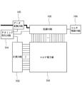
図1は本発明の一実施例に係るマルチ電子源の駆動回路のブロック図を示す。同図において、101はマルチ電子源、102は変調回路、103は走査回路、104はタイミング発生回路、105はデータ変換回路、106はマルチ電源回路である。本構成により、マルチ電子源101を駆動する。マルチ電子源101は、図34に示すように行方向配線2と列方向配線3の交点に電子源(電子放出素子)1が構成されたものである。電子源としては、前述のようにSCE型、FE型およびMIM型の電子放出素子が知られているが、本実施例では、SCE型の電子放出素子を用いた。
【0103】
データ変換回路105は、外部からマルチ電子源101を駆動する駆動データを変調回路102に適したフォーマットに変換する回路である。変調回路102はマルチ電子源101の列方向配線に接続されており、データ変換回路105からのデータ変換された駆動データに応じてマルチ電子源101に変調信号を入力する回路である。走査回路103はマルチ電子源101の行方向配線に接続されており、変調回路102の出力をマルチ電子源101のどの行に信号を加えるかを選択する回路である。一般的には、一行ずつ順次行選択する線順次走査を行うが、これに限定されることなく、複数の行を選択しても面を選択しても構わない。タイミング発生回路104は、変調回路102、走査回路103およびデータ変換回路104の各回路のタイミング信号を発生する回路である。マルチ電源回路106は、複数の電源値を出力する電源回路であり、変調回路102の出力値を制御する回路である。一般的には、電圧源回路であるが、これに限定されるものではない。
【0104】
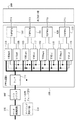
次に図2のブロック図により、変調回路102の詳しい説明をする。図2は、変調回路102の内部構成を現したブロック図である。変調回路102は、シフトレジスタ107、PWM回路108および出力段回路109で構成される。シフトレジスタ107には駆動データをデータ変換回路105でフォーマット変換された変調データが入力され、シフトレジスタ107によりマルチ電子源101の列方向配線に応じた変調データが転送される。出力段回路109はマルチ電源回路106に接続され、本発明に従った駆動波形を出力する回路である。PWM回路108はシフトレジスタ107からマルチ電子源101の列方向配線に応じた変調データが入力され、出力段回路106のそれぞれの出力電圧に応じたパルス幅出力を発生する回路である。また、シフトレジスタ107およびPWM回路108の制御のためのタイミング信号がタイミング発生回路104から入力される。
【0105】
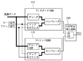
さらに、図3のブロック図により、PWM回路108の詳しい説明をする。図3は、PWM回路108の内部構成を現したブロック図である。ここでは4段の電圧出力段回路の場合を例に説明を行うが、これに限定されるものではない。PWM回路108は、ラッチ110、V1スタート回路111、V2スタート回路112、V3スタート回路113、V4スタート回路114、V1エンド回路115、V2エンド回路116、V3エンド回路117、V4エンド回路118、V1PWM発生回路119、V2PWM発生回路120、V3PWM発生回路121およびV4PWM発生回路122で構成される。ラッチ回路110では、各シフトレジスタ107から出力された各変調データをタイミング発生回路104から出力されたロード信号に応じてラッチする。ここで、タイミング発生回路104から出力されたロード信号は各PWM信号のスタートのタイミング信号にも用いている。
【0106】
ラッチ回路110でラッチされた変調データは、さらに、V1からV4のスタート回路111〜114と、V1からV4のエンド回路115〜118に入力される。次に、V1スタート回路111から出力されたスタート信号とV1エンド回路115から出力されたエンド信号がV1PWM回路119に入力され、出力電圧V1に対応するPWM出力が出力段回路109に入力される。同様に、V2スタート回路112から出力されたスタート信号とV2エンド回路116から出力されたエンド信号がV2PWM回路120に入力されて出力電圧V2に対応するPWM出力が出力段回路109に入力され、V3スタート回路113から出力されたスタート信号とV3エンド回路117から出力されたエンド信号がV3PWM回路121に入力されて出力電圧V3に対応するPWM出力が出力段回路109に入力され、V4スタート回路114から出力されたスタート信号とV4エンド回路118から出力されたエンド信号がV4PWM回路122に入力されて出力電圧V4に対応するPWM出力が出力段回路109に入力される。
【0107】
ここでは、本発明に従った駆動波形を作成するために、V1スタート回路111から出力されたスタート信号よりもV2スタート回路112から出力されたスタート信号が、V2スタート回路112から出力されたスタート信号よりもV3スタート回路113から出力されたスタート信号が、V3スタート回路113から出力されたスタート信号よりもV4スタート回路114から出力されたスタート信号が遅いタイミングで出力される。さらに、V4エンド回路118から出力されたエンド信号よりもV3エンド回路117から出力されたエンド信号が、V3エンド回路117から出力されたエンド信号よりもV2エンド回路116から出力されたエンド信号が、V2エンド回路116から出力されたエンド信号よりもV1エンド回路115から出力されたエンド信号が遅いタイミングで出力される。
【0108】
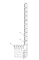
次に、V1〜V4スタート回路111〜114とV4〜V1エンド回路115〜118とV1〜V4PWM回路119〜122の詳細な説明を行う。図4に第1の回路例を、図5に第2の回路例を挙げ説明する。
【0109】
図4はマルチ電子源101の複数の変調信号配線への出力波形の立ち上がりがほぼ同時になるように揃える場合の回路構成を示した図である。ここでは、V1スタート回路111、V1エンド回路115およびV1PWM発生回路119のみを示しているが、他のスタート回路、エンド回路およびPWM発生回路は上記回路と同じ構成である。
【0110】
V1スタート回路111は、デコード回路とアップカウンタとコンパレータで構成され、V1エンド回路115は、デコード回路とアップカウンタとコンパレータで構成され、V1PWM発生回路119はRSフリップフロップで構成されている。
【0111】
V1スタート回路111内のデコード回路において変調データに含まれる制御信号によりデコードされたデータが出力される。V1スタート回路111内のデコード回路の出力値とV1スタート回路111内のアップカウンタとの出力が一致した場合に、V1スタート回路111内のコンパレータからV1スタート信号が出力される。変調データの各階調値ごと信号波形は決まるので、変調データの階調値に対応したデータを出力できるようにデコード回路は設定されている。ここで0でない階調値に対応する波高値のうちの最小波高値であるV1は変調データの階調値が0以外のときに用いるので、変調データの階調値が0以外の時には、アップカウンタの出力値との比較によってV1出力の開始を規定するスタート信号が発生されるような出力を出力するようにデコード回路は構成されている。変調データの階調値に対応する信号波形において、V2、V3、V4が必要か否かも各階調値ごとに決まっているので、V2、V3、V4のスタート回路においてもアップカウンタの出力と比較されるデータをデコード回路が変調データの階調値に応じて出力する。一方V1エンド回路111内のデコード回路において変調データに含まれる制御信号によりデコードされたデータが出力される。変調データの階調値によってV1出力を終了するタイミングが決まるので、階調値に応じた出力をデコード回路が出力する。V2、V3、V4のスタート回路においても同様である。V1エンド回路111内のデコード回路の出力値とV1エンド回路111内のアップカウンタの出力が一致した場合に、V1エンド回路111内のコンパレータからV1エンド信号が出力される。
【0112】
以上のスタート信号とエンド信号がV1PWM発生回路119に入力されることにより、V1出力に対応するPWM波形TV1が出力される。図4において、V1PWM発生回路119は、RSフリップフロップにより構成されている。このRSフリップフロップのセット端子Sにスタート信号が、リセット端子Rにエンド信号が入力されることによって、スタート信号の入力タイミングで立ち上がってエンド信号の入力タイミングで立ち下がる信号がV1PWM発生回路119のPWM波形TV1としてRSフリップフロップから出力される。なお、ここでは、V1PWM発生回路119としてRSフリップフロップを用いたが、JKフリップフロップや、他の回路でも構わない。
【0113】
次に、第2の回路例として、図5はマルチ電子源101の複数の変調信号配線への出力波形の立ち下がりがほぼ同時になるように揃える場合の回路構成を示した図である。V1スタート回路111は、デコード回路とダウンカウンタとコンパレータで構成され、V1エンド回路115は、コンスタント回路とダウンカウンタとコンパレータで構成され、V1PWM発生回路119はRSフリップフロップで構成されている。ここでは、V1スタート回路111、V1エンド回路115およびV1PWM発生回路119のみを示しているが、他のスタート回路、エンド回路およびPWM発生回路は上記回路と同じ構成である。
【0114】
V1スタート回路111内のデコード回路において変調データに含まれる制御信号によりデコードされたデータが出力される。V1スタート回路111内のデコード回路の出力値とV1スタート回路111内のダウンカウンタの出力が一致した場合に、V1スタート回路内のコンパレータからV1スタート信号が出力される。V1エンド回路111内のデコード回路において変調データに含まれる制御信号によりデコードされたデータが出力される。V1エンド回路111内のデコード回路の出力値とV1エンド回路内のダウンカウンタとの出力が一致した場合に、V1エンド回路のコンパレータからV1エンド信号が出力される。以上のスタート信号とエンド信号がV1PWM発生回路119に入力されることにより、V1出力に対応するPWM波形TV1が出力される。
【0115】
上述のPWM回路108および出力段回路109は、マルチ電子源101の各列方向配線に対応して、図4または図5のいずれかに示される回路を用いることができるが、第3の例として、列方向配線に、図4の回路と図5の回路を交互に設けることにより、立ち上がり揃えと、立ち下がり揃えを交互に行うこともできる。
【0116】
図6は、図2および図3に示す出力段回路109として列方向配線1本当たり用いられる回路の一例を示す。図6の回路において、電位V1〜V4は、0<V1<V2<V3<V4であり、それぞれPWM出力波形TV1〜TV4に対応して出力される。Q1〜Q4はオンすることによりそれぞれ電位V1〜V4を出力端子Outに出力するトランジスタまたはペアトランジスタである。PWM出力波形TV1〜TV4は、これらのうち2つ以上がHレベルであっても2個以上のトランジスタQ1〜Q4が同時にオンすることがないように、かつHレベルであるPWM出力波形TV1〜TV4に対応する電位V1〜V4のうち最大のもののみが出力端子Outに出力されるように、論理回路を介して各トランジスタQ1〜Q4のゲートGV1〜GV4に印加される。図39はTV4〜TV1およびGV4〜GV0の波形の一例を示す。
【0117】
図7はLEDや電子放出素子のような電圧/発光強度特性が非線形のしきい値特性を持つ発光素子の電圧/発光強度特性を示す。横軸が印加電圧で縦軸が発光強度を表す。発光強度の比が1:2:3:4になるように、V1、V2、V3、V4の各駆動レベル電位を設定することによって発光量の時間変化グラフ中のa、b、c、dの各領域の発光量は等価となる。つまり、V1、V2、V3、V4の各駆動レベル電位を最適に設定することによって、駆動波形の時間変化グラフ中で表される単位パルス幅Δtと単位波高値すなわち電圧差V4−V3、V3−V2、V2−V1、V1−V0で構成されるA、B、C、Dの単位駆動波形ブロックの発光量を等しくすることができる。ここでは、各単位駆動波形ブロックA〜Dの発光量が輝度データの1LSB(1階調)に概ね一致するように電位V1〜V4を定めている。
【0118】
なお、素子には基礎電位として走査信号配線により選択電位が与えられる。ここでは選択電位は−9.9[V]である。よって素子に印加される電圧は電圧降下の影響を無視して考えると、駆動信号のレベルがV1、V2、V3、V4のとき、それぞれV1−(−9.9)[V]、V2−(−9.9)[V]、V3−(−9.9)[V]、V4−(−9.9)[V]である。なお、V0−(−9.9)[V]が素子の駆動電圧しきい値以下になるようにV0を選ぶ。ここではV0をグランド電位としている。またここではこの値は素子の駆動しきい値と同じにしている。すなわち素子の駆動電圧しきい値は9.9[V]である。
【0119】
図8は階調を表現するための駆動波形の形状の一例としてV14駆動波形を示す。図8において、各階調の信号は、その階調数に応じた個数の単位駆動波形ブロックからなる。1階調は1個の単位駆動波形ブロック、2階調は2個の単位駆動波形ブロック、そしてN階調はN個の単位駆動波形ブロックからなる。図中、N階調目の白抜きの単位駆動波形ブロックはN−1階調からの差分を表す。N−1階調目の駆動波形に単位駆動ブロックを、駆動波形が連続する位置に付加することによってN階調目の駆動波形を形成する。このように駆動波形を形成することによって電圧/発光強度特性が変化した場合や、発光素子間のばらつきがあった場合にも単純増加性を保証することができる。
【0120】
本実施例においては、データビット長R=10の画像データを表示するために、P=9ビットを用いてスロット幅Δtの単位パルスを0〜259個の範囲でパルス幅制御し、残りの1ビットを含むQ=2ビットを用いて波高レベルが1〜4レベルすなわち波高値V1からV4の範囲で波高値(振幅)制御する。つまり10ビットの画像データを表示するために前記R、P、Qの各データはR<P+Qなる関係を持つ。
【0121】
R=P+Qである場合、例えば、波高値制御に上位2ビットを使い、残りの8ビットでパルス幅の制御を行うと、駆動波形の立ち下がり部を階段状にした場合には10ビットのすべての画像データを表現することができない。すなわち階調数が低下する。しかし、本実施例では、R<P+Qとなるように、パルス幅の制御を9ビットで行っており、これにより、10ビットのすべての画像データを表現することができる。
【0122】
図8に示すように、N階調目の最高駆動レベルがkのとき駆動波形の立ち上がり時に1レベル(電位V1)からkレベル(電位Vk)の駆動波形を低いレベルから高いレベルに順番にすべてのレベルを出力し、かつ各レベルの出力を単位パルス幅Δt以上保持することによって、駆動波形の立ち上がり時に流れる電流を低減することが可能となる。
【0123】
同様に駆動波形の立ち下がり時にもkレベル(電位Vk)から1レベル(電位V1)の駆動波形を高いレベルから低いレベルに順番にすべてのレベルを出力しかつ、各レベルの出力を単位パルス幅Δt以上保持することによって、駆動波形の立ち下がり時に流れる電流を低減することが可能となる。
【0124】
図12にマルチ発光素子の等価回路を示す。実際の駆動においては選択する行方向配線2に選択電位を印加して、列方向配線3に駆動電位を印加するが、直感的理解のためにモデルを単純化して、図13に示す単ビット列方向配線モデルを使ってシミュレーションを行った。寄生抵抗は10Ω、寄生インダクタンスは300nH、寄生容量は10pF、変調回路は4種の電源とMOSトランジスタによって形成した。
【0125】
図13の回路について図8中の9階調の駆動波形をV0=0V、V1=3V、V2=3.7V、V3=4.4V、V4=5.0Vの条件で駆動した場合のシミュレーションを行った。行方向配線末端の電圧波形を図14に、列方向配線に流れ込む電流波形を図15に示す。
【0126】
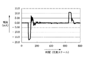
比較のためにV0=0V、V1=V2=V3=V4=5.0Vの条件で駆動した場合、つまり従来波形で駆動した場合の行方向配線末端の電圧波形を図16に、列方向配線に流れ込む電流波形を図17に示す。
【0127】
本実施例の駆動波形(図8)で駆動した場合には列方向配線に流れ込む電流が従来波形での駆動に比べて半分程度に収まっていることが分かる。その結果、従来波形で駆動した場合はオーバーシュート電圧は2V程度も発生しているのに比べ本実施例の駆動波形で駆動し場合にはオーバーシュート電圧は0.8V程度に収まっている。
【0128】
すなわち、本実施例によれば、安価な駆動回路で、高階調の実現、階調の単純増加性の確保、発光素子の均一発光、放射ノイズの低減、駆動波形の安定化が可能となる駆動波形および駆動方法を提供することが可能となる。
【0129】
[第2の実施例]
図18は、V14駆動波形の他の例を示す。図8の駆動波形は、図7に示すように、発光強度の比が1:2:3:4になるように、V1、V2、V3、V4の各駆動レベル電位を設定した場合の例を示した。LEDや電子放出素子において、発光強度は駆動電流に概ね比例するので、以下これを電流等分割方式と呼ぶ。一方、図18は、図19に示すように、V1、V2、V3、V4を、それらの比が1:2:3:4になるように、すなわち電位差V4−V3、V3−V2、V2−V1およびV1−V0(ここでも駆動波形の基準電位V0を素子の駆動しきい値と同じにした)が一定となるように定めたもので、以下これを電圧等分割方式と呼ぶ。図19は電圧等分割方式における電圧/電流(発光強度)を示す。
【0130】
図18において、N階調目の白抜きの単位駆動波形ブロックはN−1階調からの差分を表す。N−1階調目の駆動波形に1個の単位駆動ブロックを、駆動波形が連続する位置に付加することによってN階調目の駆動波形を形成する。図18において用いる図19の単位駆動ブロックA〜Dの発光量a〜dはa<b<c<dの関係にある。そのため、単位駆動ブロックA〜Dの発光量が一定である図8の波形においては、3階調と4階調との差分は単位駆動ブロックBであるのに対し、図18の波形においては、単位駆動ブロックAとして低階調である3階調と4階調との間の変化を小さくしている。
【0131】
図20にV14駆動における直線性を示す。このように駆動波形を形成することによって電圧、発光強度特性が変化した場合や、発光素子間のバラツキがあった場合にも単純増加性を保証することができる。
【0132】
図18に示すように、N階調目の最高駆動レベルがkのとき駆動波形の立ち上がり時に1レベル(電位V1)からkレベル(電位Vk)の駆動波形を低いレベルから高いレベルに順番にすべてのレベルを出力し、かつ各レベルの出力を単位パルス幅Δt以上保持することによって、駆動波形の立ち上がり時に流れる電流を低減することが可能となる。
【0133】
同様に駆動波形の立ち下がり時にもkレベル(電位Vk)から1レベル(電位V1)の駆動波形を高いレベルから低いレベルに順番にすべてのレベルを出力しかつ、各レベルの出力を単位パルス幅Δt以上保持することによって、駆動波形の立ち下がり時に流れる電流を低減することが可能となる。
【0134】
[第3の実施例]
図21は、Vn駆動波形の一例を示す。この波形は、輝度データがRビットから構成される時に、輝度データが概略0<N≦((2R)k/n−1)の時、データNの駆動波形の波高値をk(kは1以上n未満の整数)とする波形で駆動するためのものである。図8の駆動波形では、波高値kが3以下の場合、n−2階調目の駆動波形に単位駆動ブロックを付加することによってn−1階調目の駆動波形の波高値kの単位駆動ブロック数(スロット数)が3になったとき、次のn階調目の駆動波形では波高値k+1の単位駆動ブロックを付加していたのに対し、図21の駆動波形では、階調を増加する際、波高値1(1レベル;最低波高値)の単位駆動ブロック数が所定の最大数S(本実施例では259)に達するまでは、波高値(レベル)の繰上げを行わず、最大数Sに達して次に1階調増加するときに、1レベルの単位駆動ブロック数が(S・k+2k+1)/(k+1)以上のこれに最も近い数となり、かつそれぞれ1つ上のレベルのブロック数が下のものより2個または3個少なくなるように折り返して、繰上げを行っている。
【0135】
例えば、S=259の場合、259階調目で1レベルの単位駆動ブロック数が259個と一杯になると、次の260階調目では1レベルが131個と2レベルが129個になり、同様に、516階調目で1レベルが259個と2レベルが257個となって1レベルの単位駆動ブロック数が一杯になると、次の517階調目では、1レベルが175個と2レベルが172個と3レベルが170個になり、771階調目で1レベルが259個と2レベルが257個と3レベルが255となって1レベルの単位駆動ブロック数が一杯になると、次の772階調目では、1レベルが196個と2レベルが194個と3レベルが192個と4レベルが190個になり、最大波高値が1つずつ繰り上がる。
【0136】
図21の駆動波形によると、n=4、k=1すなわち輝度データが0〜最大輝度の1/4までの場合は、従来のパルス幅変調波形に対し、パルス幅変調波形の振幅の実効部分を1/4にし、パルス幅を4倍にして駆動を行うことにより、発光素子1素子当たりに流れる電流はi/4となり、選択された行方向配線に流れる電流もr*i/4となる。したがって電圧降下量も1/4に低減することが可能となり発光素子に印加される電圧の減少量も1/4に低減することが可能となる。同様にn=4、k=2すなわち輝度データが0〜最大輝度の1/2までの場合は電圧降下量を1/2に、n=4、k=3すなわち輝度データが0〜最大輝度の3/4までの場合は電圧降下量を3/4に低減することが可能となる。
【0137】
図9にr×sマトリクスの画像表示装置を示す。図10にn=4、k=1すなわち輝度データが0〜最大輝度の1/4までの場合の従来技術によるパルス幅変調回路での駆動波形を示す。発光素子1素子当たりに流れる電流をiとすると選択された行方向配線Yqにはr*iなる電流が流れることにより電圧降下が発生し、発光素子に印加される電圧が減少してしまうことが分かる。
【0138】
図11にn=4、k=1すなわち最大輝度の1/4迄の輝度データの場合の本実施例によるパルス幅変調回路での駆動波形を示す。パルス幅変調波形の振幅の実効部分(振幅から素子の駆動電圧しきい値に含まれる部分を引いた部分;本実施例では変調波形の基準電位となるV0を素子の駆動しきい値と同じ値としたため、変調波形の振幅から素子の駆動電圧しきい値に含まれる部分を引いた部分=変調波形の振幅である)を1/4にし、パルス幅を4倍にした駆動を行った様子を示す。発光素子1素子当たりに流れる電流はi/4となり、選択された行方向配線に流れる電流もr*i/4となる。したがって電圧降下量も1/4に低減することが可能となり発光素子に印加される電圧の減少量も1/4に低減することが可能となる。
【0139】
同様にn=4、k=2すなわち輝度データが0〜最大輝度の1/2までの場合は電圧降下量を1/2に、n=4、k=3すなわち輝度データが0〜最大輝度の3/4までの場合は電圧降下量を3/4に低減することが可能となる。
【0140】
図22に第1または第2実施例のV14駆動(前揃え)における変調波形の例と任意の走査配線Yqに流れる電流を示す。また、図23に本実施例であるVn駆動(前揃え)における変調波形の例と任意の走査配線Yqに流れる電流を示す。本実施例のVn駆動の方が、電流が平均化されることによって走査配線に流れる電流のピークが大幅に減少しているのが分かる。
【0141】
図24にVn駆動に前後揃えを併用した場合の走査配線(行方向配線)Yqに流れる電流を示す。さらに電流が平均化されている。ここで、前揃えとは、駆動波形の立ち上がり部分が1選択期間の前半になるように制御することであり、好適には時間的に最初の単位駆動ブロックをパルス幅制御の前半の所定のスロットで発生するとよい。また、後ろ揃えとは、駆動波形の立ち下がり部分が1選択期間の後半になるように制御することであり、好適には時間的に最後の単位駆動ブロックをパルス幅制御の後半の所定のスロットで発生するようにするとよい。なお、これら所定のスロットを固定する場合は、前半の所定のスロットとして1選択期間の最初のスロットを、後半の所定のスロットとして最終スロットを設定するのが好ましいが、より内側のスロットを設定してもよい。また、各列方向配線ごとに、その列方向配線または他の列方向配線を介して駆動すべき発光素子の階調または変調波形に応じて、前半または後半の各所定のスロットを設定するようにしてもよい。あるいは同時に選択される複数の発光素子の階調または変調波形に応じてそれらを駆動する全列方向配線に対して同じスロットを、前半または後半の各所定のスロットとして設定するようにしてもよい。
【0142】
[第4の実施例]
図25に新Vn駆動波形を示す。この駆動波形は、階調を増加する際、先ず波高値1(1レベル)の単位駆動ブロックを所定の最大数S(本実施例では259)に達するまで配列し、次に2レベル(電位V2)の単位駆動ブロックを第2スロットから第S−1スロットに達するまで配列し、‥‥、kレベル(電位Vk)の単位駆動ブロックを第kスロットから第S+1−kスロットに達するまで配列するというように、順序良く配列するものである。
【0143】
図26に新Vn駆動(前揃え)における変調波形の例と任意の走査配線Yqに流れる電流を示す。電流が平均化されている。さらに新Vn駆動に前後揃えを併用することによって図27に示すように走査配線Yqに流れる電流を1H期間内でほぼ均一にすることが可能となる。
【0144】
ここで1920×3本の情報配線および1024本の走査配線を持つマトリクスパネルについて情報配線に流れる電流の低減効果を算出する。素子に流す電流を最大0.8mAとすると、図7に示すように駆動電流を等分割になるように変調波形を設定した場合、従来の単純PWMやV14駆動の場合は1素子当たりの電流変化の最大値は0.8mAであるから1走査配線当たりの電流変化の最大値ΔIyは
ΔIy=0.8mA×1920×3=4.608A
前後揃えを併用することによって1/2になるので
ΔIy=2.304A
新Vn駆動の場合は波形の立ち上がり、立ち下がり部を除いた部分では電流の変化は0.8mA/4=0.2mAであるので
ΔIy=0.2mA×1920×3=1.152A
さらに、前後揃え駆動を併用すると1素子ごとに前揃え、後ろ揃えが繰り返されるので1/2になり、
ΔIy=576mA
となる。
【0145】
[実施例の変形例]
図21のVn駆動および図25の新Vn駆動において、変調波形は、図7に示すように駆動電流が等分割になるように設定することも、図19に示すように駆動電位振幅の実効部分が等分割になるように設定することも可能である。波形の立ち上がり立ち下がり時に発生するリンギングやオーバーシュートを防止するためには、基礎電位との電位差が素子の駆動電圧しきい値となる電位(V0)、ならびにV1、V2、V3、およびV4間の電圧を等しくすることが有効である。図19に駆動電位振幅の実効部分を等分割した場合の印加電圧と発光量の関係を示す。駆動波形の時間変化グラフ中で表される単位パルス幅と単位波高値で構成されるA、B、C、Dの単位駆動波形ブロックの発光量が等しくならないことが分かる。
【0146】
図20にV14駆動において電流等分割にした場合と、電圧等分割にした場合の輝度とデータの関係を示す。低輝度領域で直線性がやや損なわれるが、単純増加性は保証されており、データの補正等によって対処可能である。
【0147】
γ補正については、リンギング発生を最小限に出来るV1〜V4の電圧等分割に設定によって、輝度データ対輝度の関係が通常使用される2.2乗の逆γ特性よりも深いカーブ(低輝度領域で輝度分解能が高くなる)となる。その結果、逆γ変換時に低輝度から中輝度の輝度分解能を高めることが可能となる。
【0148】
上述した実施例においては、4レベルの波高値制御を行い階調数が0から1023の1024階調の例を挙げたが、本発明において、制御波高値、階調数の限定は無い。
【0149】
【発明の効果】
本発明によって、安価な駆動回路で、高階調の実現、階調の単純増加性の確保、発光素子の均一発光、放射ノイズの低減、駆動波形の安定化が可能となる駆動波形、駆動方法を提供することが可能となる。また、安価な駆動回路で、輝度分布の偏りを低減することができる発光素子制御方法を提供することが可能となる。
【図面の簡単な説明】
【図1】 本発明の一実施例に係るマルチ電子源駆動回路のブロック図である。
【図2】 図1における変調回路のブロック図である。
【図3】 図2におけるPWM回路のブロック図である。
【図4】 図3のPWM回路の要部構成の一例を示すブロック図である。
【図5】 図3のPWM回路の要部構成の他の例を示すブロック図である。
【図6】 図2における出力段回路の一例を示す回路図である。
【図7】 発光素子の電圧/発光強度特性(電流等分割)を示すグラフである。
【図8】 電流等分割によるV14駆動波形の一例を示す波形図である。
【図9】 r×sマトリクスの画像表示装置の構成図である。
【図10】 輝度データが0〜最大輝度の1/4までの場合の従来技術によるパルス幅変調回路での駆動波形の波形図である。
【図11】 輝度データが0〜最大輝度の1/4までの場合の第1の実施例によるパルス幅変調回路での駆動波形の波形図である。
【図12】 図1のマルチ発光素子の等価回路図である。
【図13】 図12の等価回路図の単ビット列方向配線モデルの図である。
【図14】 図13のモデルの行方向配線末端の電圧波形図である。
【図15】 図13のモデルの列方向配線に流れ込む電流波形図である。
【図16】 従来波形で駆動した場合の行方向配線末端の電圧波形図である。
【図17】 従来波形で駆動した場合の列方向配線に流れ込む電流波形図である。
【図18】 電圧等分割によるV14駆動波形の一例を示す波形図である。
【図19】 発光素子の電圧/発光強度特性(電圧等分割)を示すグラフである。
【図20】 図8および図18のV14駆動における直線性を示すグラフである。
【図21】 Vn駆動波形の一例を示す波形図である。
【図22】 V14駆動(前揃え)における変調波形および任意の走査配線Yqに流れる電流を示す波形図である。
【図23】 Vn駆動(前揃え)における変調波形および任意の走査配線Yqに流れる電流を示す波形図である。
【図24】 Vn駆動に前後揃えを併用した場合の変調波形および任意の走査配線Yqに流れる電流を示す波形図である。
【図25】 新Vn駆動波形の一例を示す波形図である。
【図26】 新Vn駆動(前揃え)における変調波形の例と任意の走査配線Yqに流れる電流を示す波形図である。
【図27】 新Vn駆動に前後揃えを併用した場合の変調波形および任意の走査配線Yqに流れる電流を示す波形図である。
【図28】 表面伝導型放出素子の素子構成の一例を示す図である。
【図29】 FE型の素子構成の一例を示す断面図である。
【図30】 MIM型の素子構成の一例を示す断面図である。
【図31】 マルチ電子ビーム源の電気的構成を示す配線図である。
【図32】 従来の走査回路およびパルス幅変調回路の出力波形図である。
【図33】 従来の走査回路およびパルス幅変調回路の出力波形図である。
【図34】 マルチ電子源の構成図である。
【図35】 図34のマルチ電子源の分解斜視図である。
【図36】 ある選択電極に接続されている画素の全てが点灯したときの等価回路図である。
【図37】 図36の回路における選択電極上の各部の電圧を示すグラフである。
【図38】 図36の回路で最遠方端の画素に印加される駆動波形の図である。
【図39】 図6における信号TV4〜TV1およびGV4〜GV0の波形図である。
【符号の説明】
1:電子源(電子放出素子)、2:行方向配線、3:列方向配線、4:行方向配線寄生抵抗、5:列方向配線寄生抵抗、6:行方向配線寄生インダクタンス、7:列方向配線寄生インダクタンス、8:寄生容量、9:走査回路、10:変調回路、11:画像表示装置、12:基板、13:メタルバック、14:蛍光面、15:フェースプレート、16:電子源からの電流、101:マルチ電子源、102:変調回路、103:走査回路、104:タイミング発生回路、105:データ変換回路、106:マルチ電源回路、107:シフトレジスタ、108:PWM回路、109:出力段回路、110:ラッチ、111:V1スタート回路、112:V2スタート回路、113:V3スタート回路、114:V4スタート回路、115:V1エンド回路、116:V2エンド回路、117:V3エンド回路、118:V4エンド回路、119:V1PWM発生回路、120:V2PWM発生回路、121:V3PWM発生回路、122:V4PWM発生回路。[0001]
BACKGROUND OF THE INVENTION
The present invention relates to a drive circuit that generates a drive waveform corresponding to luminance data, and to a display device using the drive circuit. The present invention also relates to a driving method for generating the driving waveform. In particular, the present invention relates to a method for driving the light emitting element in an image display apparatus including an image display panel in which a plurality of light emitting elements are arranged in a matrix.
[0002]
[Prior art]
Conventionally, two types of electron-emitting devices, a hot cathode device and a cold cathode device, are known. Among these, as the cold cathode device, for example, a surface conduction type emission device, a field emission type device (hereinafter referred to as FE type), a metal / insulating layer / metal type emission device (hereinafter referred to as MIM type), and the like are known. Yes. Examples of surface conduction electron-emitting devices include M.I. I. Elinson, Radio Eng. Electron Phys. , 10, 1290 (1965) and other examples described later.
[0003]
The surface conduction electron-emitting device utilizes a phenomenon in which electron emission occurs when a current flows in parallel to a film surface in a small-area thin film formed on a substrate. As this surface conduction electron-emitting device, SnO by Erinson et al.2In addition to those using thin films, those using Au thin films (G. Dittmer: Thin Solid Films, 9, 317 (1972)), In2OThree/ SnO2A thin film (M. Hartwell and C.G. Fonstad: IEEE Trans. ED Conf., 519 (1975)) and a carbon thin film (Haraki Araki et al .: Vacuum, Vol. 26, No. 1, 22 (1983) )) Etc. have been reported.
[0004]
As a typical example of the device configuration of these surface conduction electron-emitting devices, the above-described M.P. FIG. 3 shows a plan view of a device by Hartwell et al. In the figure,
[0005]
M.M. In the surface conduction electron-emitting devices described above, including the device by Hartwell et al., The
[0006]
Examples of the FE type include, for example, W.W. P. Dyke & W. W. Dolan, Field emission, Advance in Electron Physics, 8, 89 (1956), or C.I. A. Spindt, Physical properties of thin-film field depreciation with molebdenum cones, J. Am. Appl. Phys. 47, 5248 (1976).
[0007]
As a typical example of the element configuration of the FE type, FIG. A. A cross-sectional view of the element according to Spindt et al. Is shown. In the figure,
[0008]
Examples of the MIM type include C.I. A. Mead, Operation of tunnel-emission Devices, J. MoI. Appl. Phys. , 32, 646 (1961) and the like are known. A typical example of an MIM type element configuration is shown in FIG. In the figure, 3020 is a substrate, 3021 is a lower electrode made of metal, 3022 is a thin insulating layer having a thickness of about 100 angstroms, and 3023 is an upper electrode made of a metal having a thickness of about 80 to 300 angstroms. It is. In the MIM type, electron emission is caused from the surface of the
[0009]
Since the above-described cold cathode device can obtain electron emission at a lower temperature than a hot cathode device, a heater for heating is not required. Therefore, the structure is simpler than that of the hot cathode device, and a fine device can be produced. Further, even if a large number of elements are arranged on the substrate at a high density, problems such as thermal melting of the substrate hardly occur. In addition, the response speed is low in the case of the cold cathode element, unlike the case where the response speed is low because the hot cathode element operates by heating of the heater.
For this reason, research for applying cold cathode devices has been actively conducted.
[0010]
For example, the surface conduction electron-emitting device has an advantage that a large number of devices can be formed over a large area because the structure is particularly simple and easy to manufacture among the cold cathode devices. Therefore, for example, as disclosed in Japanese Patent Application Laid-Open No. 64-31332 by the present applicant, a method for arranging and driving a large number of elements has been studied.
As for the application of the surface conduction electron-emitting device, for example, image forming apparatuses such as an image display apparatus and an image recording apparatus, and a charged beam source have been studied.
[0011]
In particular, as an application to an image display device, for example, as disclosed in US Pat. No. 5,066,883, JP-A-2-257551, JP-A-4-28137, etc., a surface conduction electron-emitting device and an electron beam are disclosed. An image display device using a combination of phosphors that emit light upon irradiation is studied. An image display device using a combination of a surface conduction electron-emitting device and a phosphor is expected to have characteristics superior to those of other conventional image display devices. For example, it can be said that it is superior in that it does not require a backlight because of its self-luminous type and has a wide viewing angle, compared with a liquid crystal display device that has become widespread in recent years.
[0012]
A method for driving a large number of FE types in a row is disclosed in, for example, USP 4,904,895. As an example of applying the FE type to an image display device, for example, R.I. A flat panel display device reported by Meyer et al. Is known (R. Meyer: Recent Development on Microtips Display at LETI, Tech. Digest of 4th Int. Vacuum Microelectronics. .
[0013]
An example in which a large number of MIM types are arranged and applied to an image display apparatus is disclosed in, for example, Japanese Patent Laid-Open No. 3-55738.
Further, as an image display device using an element other than an electron-emitting element, an apparatus using an EL (electroluminescence) element is disclosed in, for example, Japanese Patent Application Laid-Open No. 09-281928.
[0014]
The inventors of the present invention have tried a multi-electron beam source by an electrical wiring method shown in FIG. 31, for example. That is, a multi-electron beam source in which a large number of electron-emitting devices are two-dimensionally arranged and these devices are wired in a matrix as shown in the figure.
[0015]
In the figure,
[0016]
In a multi-electron beam source in which electron-emitting devices are matrix-wired, appropriate electric signals are applied to the row-direction wiring and the column-direction wiring in order to output a desired electron beam.
[0017]
FIG. 32 shows a pulse width modulation waveform. For example, in order to drive any one row of the electron-emitting devices in the matrix, the selection potential Vs is applied to the row direction wiring of the selected row, and at the same time, the non-selection potential is applied to the row direction wiring of the non-selected row. Vns is applied. In synchronization with this, a driving potential Ve for outputting an electron beam is applied to the column direction wiring. According to this method, a voltage of Ve−Vs is applied to the electron-emitting devices in the selected row, and a voltage of Ve−Vns is applied to the electron-emitting devices in the non-selected rows. If Ve, Vs, and Vns are set to appropriate potentials, an electron beam having a desired intensity is output only from the electron-emitting devices in the selected row. Further, since the response speed of the cold cathode device is high, changing the length of time for applying the drive potential Ve can also change the length of time for which the electron beam is output.
Similarly, the electron beam can also be controlled by a method called peak value modulation in which the luminance is controlled by changing the potential or current value applied to the column direction wiring.
[0018]
[Problems to be solved by the invention]
By the way, in a display device having an effective pixel number of 1920 × 1080, a frame rate of 60 Hz, and a 10-bit gradation, in the case of the pulse peak value modulation method, if the peak value of energy applied to the element is Pi, Pi / 2Ten= Pi / 1024 resolution is required. Since Pi is about several volts in the case of voltage driving, a resolution of several mV is required for the driving waveform over the entire 1920 × 1080 screen. This value is difficult to realize in consideration of the characteristics of the IC, printed circuit board, power supply, etc. that constitute the drive circuit.
[0019]
On the other hand, in the case of the pulse width modulation method, the time for driving one scanning line is 1 / (60 × 1080) ≈15 μsec. When 10-bit pulse width modulation is performed, the minimum pulse width is 1 / (60 × 1080 × 2Ten) ≈15 nsec, and a minimum pulse width resolution of 15 nanoseconds is required.
[0020]
However, the wiring as shown in FIG. 31 is equivalent to a low-pass filter having a cutoff frequency determined by wiring inductance (L), wiring capacitance (C), and wiring resistance (R). When the signal line and the display part line having such a low-pass characteristic are driven by a line sequential-pulse width modulation (PWM) driving method composed of a frequency spectrum component equal to or higher than the cutoff frequency, as shown in FIG. The rising and falling waveforms of the PWM waveform applied to the element become dull, and the display quality is lowered at low luminance. In particular, when a low gradation pulse width modulation driving waveform is applied from the information
[0021]
Even when a constant current pulse having a short time length is supplied from a controlled constant current source to a multi-electron source in which a large number of electron-emitting devices are arranged in a matrix, almost no electrons are emitted. When the constant current pulse is continuously supplied for a relatively long period of time, of course, electrons start to be emitted, but a large rise time is required before the electron emission starts.
[0022]
FIG. 33 is a time chart for explaining this. As shown in FIG. 33, even if a short current pulse is supplied from the controlled constant current source, the current If hardly flows through the electron-emitting device. Even when a long pulse is supplied, the drive current If flowing through the electron-emitting device has a waveform with a large rise time. Although the cold cathode electron-emitting device itself has high-speed response performance, the waveform of the current supplied to the electron-emitting device is lost. As a result, the waveform of the emission current Ie is also deformed. I was sorry.
[0023]
In a multi-electron source with simple matrix wiring, the parasitic capacitance (wiring capacitance) increases as the matrix size increases. The main part of the parasitic capacitance exists at the intersection of the row direction wiring and the column direction wiring, and this equivalent circuit is shown in FIG. When the supply of the constant current I1 is started from the control constant
[0024]
In addition, voltage driving has the following problems to be solved. Wiring resistance is generally designed to be low in a display using an element through which current flows as a light emitting element, for example, an LED, EL, FED, or SED. Therefore, the equivalent circuit is a model shown in FIG. 31 configured by parasitic capacitance, parasitic resistance, and parasitic inductance. When the conventional voltage driving method is applied to such a circuit, the charging current i flows into the parasitic capacitance due to the application of the voltage, so that the driving waveform rising portion becomes dull. Furthermore, an electromotive force U = −L × (di / dt) is generated due to the self-inductive action of the parasitic inductance, overshooting and ringing occur, and an abnormal voltage is applied to the light emitting element.
[0025]
In recent years, the demand for large area, high definition, and high gradation for displays has been remarkably increased, and the parasitic inductance and parasitic capacitance of wiring has increased. Crushing, overshooting and ringing are increasingly important issues to be solved.
[0026]
Further, the driving waveform by simple pulse width control and pulse peak value control has a problem that it is impossible to guarantee a simple increase in gradation due to a change or variation in voltage / light emission intensity characteristics of the light emitting element.
[0027]
Further, for example, as disclosed in Japanese Patent Application Laid-Open No. 09-319327, a control current source for supplying a driving current pulse to the cold cathode element and a voltage for charging a parasitic capacitance of the multi-electron source at high speed By the charging voltage applying means for electrically connecting the voltage source and the column-direction wiring in synchronization with the source and the rising edge of the drive current pulse, until the parasitic capacitance of the wiring is substantially charged, A method of applying a charging voltage in addition to a driving current pulse has been performed. When such driving is performed, it becomes possible to guarantee the linearity of gradation.
[0028]
Japanese Patent Laid-Open No. 8-22261 divides each word of a digital video signal into a plurality of subwords, and assigns a PWM waveform having a low peak value to a lower subword and a high peak value to an upper subword. A drive waveform having a period longer than the time slot period of the conventional PWM waveform is realized to prevent a reduction in image display quality at low luminance.
[0029]
Japanese Patent Laid-Open No. 10-39825 discloses a second pulse width modulation output means for outputting a binary signal having a high voltage V1 and a low voltage V2 in accordance with a luminance signal, and in accordance with the luminance signal, The frequency of the pulse width modulation circuit can be reduced by the driving method having the second pulse width signal output means for cutting the binary signal with a predetermined pulse width, and the PWM operation frequency which becomes a problem with the increase in gradation is increased. The problem is solved.
[0030]
Furthermore, in Japanese Patent Application Laid-Open No. 11-015430, information on M × N gradation defined by pulse width control corresponding to M gradation and pulse peak value control corresponding to N gradation is included as a voltage pulse. High gradation can be easily realized by using the pulse drive waveform.
[0031]
However, in the conventional driving by pulse width modulation, there is a possibility that a large electromagnetic noise, that is, unnecessary radiation of the electromagnetic wave may be induced when the driving waveform rises and falls depending on the gradation.
[0032]
Further, in a multi-electron beam source in which a large number of the above-described electron-emitting devices are arranged in a matrix, the voltage applied to each device is a device far from the power supply end due to a voltage drop caused by the resistance of the wiring. As a result, there is a problem that the emission electron distribution of each element is not uniform. When this multi-electron emitting device is applied to an image display device, there is a problem that image quality deteriorates due to a voltage drop caused by wiring resistance.
[0033]
This will be described with reference to FIGS. 34 and 35. FIG. 34 shows an example of a multi-electron beam source substrate. In the figure, 1 is an electron-emitting device, 2 is a selection electrode (row direction wiring), 3 is an information electrode (column direction wiring), 9 is a selection circuit, 10 is a modulation circuit, and 12 is a substrate.
[0034]
FIG. 35 is a perspective view of an image display panel using the multi-electron
[0035]
Now, it is assumed that a
[0036]
Here, the current flowing into the selection electrode is assumed to be the same value If in each element, and the resistance value of the selection electrode per pixel is assumed to be rf. The potential on the selected electrode at this time is calculated.
[0037]
The current flowing through Rf5 is If, and the voltage drop due to Rf5 is If · rf. The current flowing through Rf4 is 2 · If, and the voltage drop due to Rf4 is 2 · If · rf. FIG. 37 shows the result of calculating the voltage drop in each resistance component and calculating the potential of each part on the selected electrode. Here, the case where Ve> Vs is shown.
[0038]
It should be noted that when the potential Vs is output from the
[0039]
This variation in voltage is not a problem when the resistance component of the selection electrode is very small. However, if the resistance component of the selection electrode is large due to, for example, an increase in the screen size of the image display device, the voltage variation cannot be ignored. It will be a thing. Further, when the number of pixels increases and the current flowing into the selection electrode increases, the voltage variation becomes large.
[0040]
Due to this voltage variation, the voltage applied to the electron-emitting device differs from device to device. In particular, the same voltage is applied to the electron-emitting device close to the feeding point and the electron-emitting device far from the feeding point. In other words, a difference occurs in the amount of emitted electrons. This appears as a luminance difference between pixels which are elements that emit light by the electron beam emitted from the electron-emitting element, leading to a reduction in display quality as an image display device.
[0041]
In JP-A-10-112391, attention is paid to resistance values of wiring electrodes and current flowing in the wiring electrodes of an XY matrix type organic EL display device, and data electrodes are arranged on a low resistance side wiring and scanning electrodes are arranged on a high resistance side. The driving method is such that the driving voltage Vcc is driven by a current source connected to the voltage source of the driving voltage Vcc and the driving voltage Vcc at this time varies in wiring resistance depending on the position of the light emitting element as a pixel. It is disclosed that even if the current source is set to a specific voltage or higher that satisfies the condition for the constant current operation, a large number of light emitting elements can emit light uniformly and excellent characteristics as an image display device can be realized. .
[0042]
Japanese Patent No. 3049061 describes that the fall of the signal applied to the modulation wiring (information signal wiring) is divided into a plurality of steps.
In Japanese Patent Laid-Open No. 7-181917, a plurality of voltages corresponding to one or a plurality of unit drive blocks are used, and the unit drive blocks are stacked in the pulse width and peak value directions to create a drive waveform. A method is described.
[0043]
An object of the present invention is to realize a preferable driving waveform of a signal for driving a light emitting element, and in particular, to realize a driving waveform capable of accurately driving the light emitting element.
[0047]
[Means for Solving the Problems]
BookOne of the inventions of a light emitting element driving circuit according to the application is configured as follows.
ThePulse width is controlled in units of lot width Δt and the peak value in each slotIs A 1~ AnN stages (where n is an integer of 2 or more and 0 <A1<A2<・ ・ ・ ・ <An And A 1 Is the peak value corresponding to non-zero gradation data)Any ofPeak valueInDrive waveform to be controlledDuring one selection periodLight emitting elementTo supplyDrive circuitSoThe drive waveform isCrest value isCrest value A1Wave height Ak-1UntilWave ofHigh priceThe part controlled byPredetermined peak value A after at least one slotk(However, k is an integer from 2 to n)Part controlled byThe part that stands up to,Crest value isThe predetermined peak value Ak The part controlled byFromCrest value isThe peak value Ak-1Wave height A1UntilWave ofHigh priceThe part controlled byA driving circuit for a light emitting device, characterized by having a portion that falls through at least one slot.Road.
This inventionAccording to, the drive waveform can be raised and lowered in stages.It becomes possible to drive the light emitting element accurately.When the rising portion of the drive waveform has a portion that rises to a peak value higher than the peak value Ak, it is not preferable to rapidly increase the drive waveform after reaching the peak value Ak. Therefore, in the above invention, the peak value Ak is desirably the maximum peak value (at least at the rising portion) of the drive waveform.
[0048]
In each of the inventions described above, the peak value A at the rising edge of the drive waveform.1The peak value immediately before rising to the peak may be a peak value at which the light emitting element is not substantially driven. The peak value A at the falling part of the drive waveform1The peak value immediately after falling from the peak may be a peak value at which the light emitting element is not substantially driven. Here, the peak value at which the light emitting element is not substantially driven is a peak value at which the light emitting element does not emit light corresponding to the lowest gradation of the luminance data even when the peak value is input for one slot. Is selected so that the peak value does not exceed the driving threshold value of the light emitting element.
[0049]
Consider a state in which a basic potential (for example, a selection potential in matrix driving described later) is applied to the light emitting element. When the driving waveform according to the present invention is applied to this light emitting element, the potential corresponding to each part of the driving waveform (the potential when the peak value control is performed by the potential control, the potential when the peak value control is performed by the current control, A potential difference between the basic potential and a potential for passing a current is applied to the light emitting element. The peak value when light emission that cannot be ignored in display according to the luminance data due to this potential difference is the drive threshold value of the light emitting element.
[0050]
It is preferable that the peak value at which the light emitting element before the drive waveform rises to A1 is not substantially driven and the peak value at which the light emitting element after the drive waveform falls from A1 are not substantially driven have the same value. Can be adopted. In addition, when referring to the magnitude (high / low) of the crest value, the larger (high) crest value means that the crest value gives more driving energy to the light emitting element, and it always matches the magnitude relation of the potential. is not. For example, when a predetermined potential is applied as the basic potential and the potential of the drive waveform is set to a lower potential, the peak value is higher when the potential is lower.
[0051]
In the above configuration, the drive waveform is suitably set by defining the relationship between a certain drive waveform and another drive waveform in which the drive waveform increases or decreases the drive energy for driving the light emitting element as follows. It becomes possible. That is, when the slot in which the driving waveform rises to the peak value A1 is defined as the first slot, the peak values of the first to (k-1) th slots are respectively A1~ Ak-1, Kth and Nthk+ K-1 slot (however, NkIs an integer of 1 or more)k, Nthk+ K to NthkThe peak values of +2 (k−1) slots are Ak-1~ A1The driving waveform obtained by increasing the driving energy for driving the light emitting element by one step with respect to the driving waveform becomes Nth of the driving waveforms.k+ 2k-1 slot peak value is A1After that, the driving waveform obtained by sequentially increasing the driving energy by one step is further increased from the driving waveform of the previous step by the Nth.k+2 (k-1) slot peak value is A1To A2N ... Nthk+ K slot peak value is Ak-1To AkIt is to have the waveform changed to.
[0052]
That is, the peak value AkWave height AkA driving waveform in which the energy for driving the light emitting element is increased by one step with respect to a driving waveform having a portion where the light emitting element falls to a peak value at which the light emitting element is not substantially driven after passing through each lower peak value one slot at a time. The peak value is A at the falling part of the drive waveform in the previous stage.1The peak value of the slot following the slot that was1The drive waveform that increases the energy for driving the light emitting element step by step increases the peak value in the previous drive waveform by one step relative to the previous drive waveform. It is preferable to have a waveform obtained by increasing the peak value of the slot immediately before the set slot by one step.
[0053]
The invention described here defines the waveform of the drive signal, and the second drive waveform when the one-stage drive energy is increased with respect to the first drive waveform corresponding to a certain gradation energy is the present invention. Is not limited to the timing of applying the first and second drive waveforms in a predetermined period, for example, when the first drive waveform is used, the first slot from the second slot in the predetermined period is used. In the configuration in which the drive waveform is raised, the present invention includes an embodiment in which the second drive waveform is raised from the first slot of the predetermined period when the second drive waveform is used. That is, the embodiment of the present invention is the same in a predetermined period (for example, one selection period when matrix driving is performed as described later) having the rising timing of the first driving waveform and the rising timing of the second driving waveform. It is not restricted to the structure which is.
[0054]
In each invention described above, the following may be used. That is, the peak value AkWave height AkA drive waveform obtained by increasing the energy for driving the light-emitting element by one step with respect to a predetermined drive waveform having a portion where each lower peak value falls in order through at least one slot falls in the preceding drive waveform. The peak value is A in the part1The peak value of the slot following the slot that was1The drive waveform that increases the energy for driving the light emitting element step by step increases the peak value in the previous drive waveform by one step relative to the previous drive waveform. The driving method is characterized by having a waveform obtained by increasing the peak value of the slot immediately before the set slot by one step.
By setting the relationship between the drive waveforms in this way, the peak value can be changed within one stage in the slots that are continuous at the falling portion of each drive waveform.
[0055]
In particular, the drive waveform in which the energy for driving the light emitting element is increased by one step with respect to the drive waveform in the previous stage, but the slot in which the peak value is increased by one step with respect to the drive waveform in the previous stage is obtained The relationship of having a waveform in which the peak value of the immediately preceding slot is increased by one step is that the peak value of the slot in which the drive waveform determined by the relationship is increased relative to the previous drive waveform is the peak value. AkA configuration in which a series of drive waveforms up to a drive waveform having a peak value that is one step higher than that can be suitably employed. In the drive waveform in which the drive energy is further increased by one step with respect to the last drive waveform of the series of drive waveforms, the peak value is A and the peak value is A at the falling portion of the last drive waveform.1The peak value of the slot following the slot that was1It is sufficient to have the waveform changed to.
[0056]
Also, the peak value AkIs the maximum allowable peak value, or when it is desired to avoid updating the peak value as much as possible, the following may be performed. That is,
A drive waveform in which the energy for driving the light emitting element is increased step by step with respect to the drive waveform in the previous stage is a slot in which the peak value is increased by one step with respect to the drive waveform in the previous stage in the previous drive waveform. The relationship that the waveform having the peak value of the immediately preceding slot is increased by one step indicates that the peak value of the slot in which the drive waveform determined by the relationship increases the peak value with respect to the previous drive waveform is the peak value A.kIn this configuration, a series of drive waveforms up to the drive waveform is satisfied. In the drive waveform in which the drive energy is further increased by one step with respect to the last drive waveform of the series of drive waveforms, the peak value is A and the peak value is A at the falling portion of the last drive waveform.1The peak value of the slot following the slot that was1It is sufficient to have the waveform changed to.
[0057]
Further, a series of drive waveforms having different drive energies step by step may be set as follows. That is,
The drive waveform has a peak value A1Is the first slot, the peak values of the first to (k-1) -th slots are A, respectively.1~ Ak-1, Kth and Nthk+ K-1 slot (however, NkIs an integer of 1 or more)k, Nthk+ K to NthkThe peak values of +2 (k−1) slots are Ak-1~ A1The driving waveform obtained by reducing the driving energy for driving the light emitting element by one step with respect to the driving waveform becomes the peak value of the kth slot of the driving waveform as AkTo Ak-1Thereafter, the driving waveform obtained by sequentially reducing the driving energy by one step is set to the peak value of the (k−1) -th slot with respect to the driving waveform of the previous step.k-1To Ak-2..., the peak value of the first slot is A1FromCauses light emission corresponding to the lowest gradation of the luminance data.It is the structure which has the waveform changed into the no crest value.
[0058]
The present invention also defines the waveform of the drive signal, and the second drive waveform when the one-step drive energy is reduced with respect to the first drive waveform corresponding to a certain gradation energy conforms to the present invention. In this case, the timing of applying the first and second drive waveforms in a certain period is not limited. For example, when the first drive waveform is used, the first drive waveform from the first slot in the predetermined period is used. In the startup configuration, when the second drive waveform is used, the invention includes an embodiment in which the second drive waveform is started up from the second slot of the predetermined period. That is, according to the embodiment of the present invention, a predetermined period having a falling timing of the first driving waveform and a falling timing of the second driving waveform (for example, one selection period when performing matrix driving as described later). However, the configuration is not limited to the same.
[0059]
It can also be said as follows. That is,
Crest value AkEach lower peak value goes through at least one slot in turn and the peak value AkDrive waveform having a portion that rises up to a point where the energy for driving the light emitting element is reduced by one step, and the peak value is A at the rise portion of the drive waveform of the previous stage.k-1It is a slot following the slot that was, and the peak value is AkThe peak value of the slot that wask-1After that, the drive waveform in which the energy for driving the light emitting element was decreased step by step, the peak value was decreased by one step in the previous drive waveform relative to the previous drive waveform. In this configuration, the wave height value of the slot immediately before the slot is reduced by one step.
[0060]
In each invention described above, the peak value is A.kThe crest value in the slot between two slots is AkIs preferable. Since the peak value can be maintained at portions other than the rising portion and the falling portion, the light emitting element can be driven more accurately and the generation of the drive waveform is facilitated.
[0061]
It is also preferable to set as follows. That is,
The peak value is AkWhen there is another slot between two slots, the peak value in the other slot is AkAnd the peak value A including the case of k = 1.kIs AnThe peak value is reduced by increasing the driving energy by one step relative to the previous driving waveform.kThe drive waveform in which the drive energy is further increased by one step with respect to the drive waveform in which the number of slots is changed from 2 to 3, the peak value of the drive waveform is AkThe peak value of the middle slot among the three slotskTo Ak + 1It is the structure characterized by having the shape changed into.
[0062]
In addition, the driving waveform in which the driving energy for driving the light emitting element is increased over the predetermined driving waveform has priority given to increasing the pulse width over increasing the maximum peak value with respect to the predetermined driving waveform. It is also preferable to have a shape.
[0063]
When the drive energy is increased, an effect of reducing the instantaneously flowing current can be expected by prioritizing the increase of the pulse width over the increase of the peak value. Here, a preferred configuration in the case where priority is given to an increase in pulse width over an increase in peak value, is a pulse having any peak value while maintaining a shape that rises or falls while passing through each peak value by at least one slot. When the drive energy can be increased by extending the width, the maximum peak value is not increased.
[0064]
It is also preferable to set as follows. That is,
The driving waveform when the driving energy for driving the light emitting element is increased by one step with respect to the predetermined driving waveform to increase the maximum peak value of the driving waveform is the peak value difference An-An-1, ... or A2-A1Or peak value A1And the number of unit driving waveform blocks determined by the peak value difference between the peak value and the driving threshold value of the light emitting element and the slot width Δt are increased by one from the number used in the predetermined driving waveform, It is the structure which has the shape re-stacked so that the maximum peak value may continue as much as possible.
[0065]
When the drive energy is increased, an effect of reducing the instantaneously flowing current can be expected by prioritizing the increase of the pulse width over the increase of the peak value. However, even in the configuration in which the pulse width is increased in order to increase the drive energy, it is necessary to use a higher peak value at a predetermined stage when there is a limitation on the pulse width of the drive waveform. When emphasizing the continuity of the peak value, especially the maximum peak value, the unit that configures the drive waveform so that the maximum peak value continues as much as possible within the range that satisfies the staircase rise, the staircase fall, or both It is preferable to reshape the drive waveform block.
[0066]
It is also preferable to set as follows. That is,
A driving waveform in which driving energy for driving the light emitting element is increased with respect to a predetermined driving waveform is a peak value difference A.n-An-1, ... or A2-A1Or peak value A1A unit drive waveform block determined by the difference between the peak value and the peak value serving as the drive threshold value of the light emitting element, and the slot width Δt, the maximum peak value A including k = 1kIt is the structure which has the shape added preferentially to the position where becomes lower. In particular, a driving waveform obtained by increasing the driving energy for driving the light emitting element with respect to a predetermined driving waveform has a peak value difference A.n-An-1, ... or A2-A1Or peak value A1The unit drive waveform block determined by the difference between the peak value and the peak value serving as the drive threshold value of the light emitting element and the slot width Δt is preferentially placed at a position where the maximum peak value is lower and the maximum peak value continues. A configuration having an added shape can be suitably employed.
[0067]
Specifically, the drive energy is obtained by adding the unit drive waveform block to the drive waveform in which the maximum number of slots is S and the number of slots having the maximum peak value Ak is S-2 (k-1). Drive waveform further increased by one step, the peak value of any slot among the (k + 1) th to (Sk) th slots is represented by A.kTo Ak + 1It is the drive waveform which has the shape changed into. The peak value is AkTo Ak + 1The slot to be changed to, for example, may be either the (k + 1) th or the (S−k) th slot.
[0068]
In the present invention, the number of the unit drive waveform blocks is set as the drive waveform when the drive energy for driving the light emitting element is increased by one step with respect to the predetermined drive waveform to increase the maximum peak value of the drive waveform. A configuration having a shape in which the maximum peak value is re-stacked so that the maximum peak value continues as much as possible by one more than the number used in the predetermined drive waveform, and the unit drive waveform block includes a maximum peak value including k = 1 AkIt also includes an intermediate configuration with a configuration having a shape that is preferentially added to a position where is lower. That is, when the drive energy for driving the light emitting element is increased by one step with respect to the predetermined drive waveform to increase the maximum peak value of the drive waveform, the number of the unit drive waveform blocks is set to the predetermined drive waveform. In this configuration, the number is increased by one more than the number used in the waveform, and the maximum peak value is restacked so that two or more slots continue.
[0069]
Furthermore, the present invention includes a configuration in which the maximum peak values of two slots or more are not continuous. That is, when the drive energy for driving the light emitting element is increased by one step with respect to the predetermined drive waveform to increase the maximum peak value of the drive waveform, the number of the unit drive waveform blocks is set to the predetermined drive waveform. In this configuration, the number is increased by one more than the number used in the waveform, and is restacked so that the maximum peak value becomes 2 slots or more.
[0070]
In each of the above inventions, the peak value is A.1The drive waveform having a slot width of Δt preferably has drive energy for causing the light emitting element to emit light with a luminance corresponding to approximately 1 LSB of luminance data.
[0071]
Also, the peak value A1~ AnCan be suitably employed, each having a different potential value, for example, the peak value A1~ AnCan adopt a configuration in which the luminance of the light emitting element is approximately 1: 2:...: N. Also, the peak value A1~ AnIs the wave height difference Am-Am-1(Where m is an integer from 1 to n, A0Is a potential at which the driving threshold value of the light emitting element is substantially constant. Also, the peak value A1~ AnA configuration with different current values can also be adopted.
[0072]
Also, the peak value difference Am-Am-1(Where m is an integer from 1 to n, A0Is the driving threshold value of the light emitting element) is substantially constant, or A for 2 or more mm-Am-1≧ Am-1-Am-2And the peak value A including the case of k = 1.kIs the maximum peak value of the driving waveform and the peak value AkIs AnSmaller and the peak value is AkThe peak value of the slot sandwiched between the slots is AkAnd said NkWhen the driving energy is further increased by one step with respect to the driving waveform in which +2 (k−1) has reached a predetermined maximum number of slots S (where S is an integer of 2n−1 or more), the peak value is A1A peak value of a slot that is adjacent to the slot and has a peak value at which the light emitting element is not substantially driven is defined as A1Instead of changing to1Is the closest integer greater than or equal to (S · k + 2k + 1) / (k + 1) and the maximum peak value is Ak + 1And,PreviousWave height difference Am-Am-1And the number of unit drive waveform blocks determined by the slot width Δt is one more than the drive waveform.And related to this applicationDriveAs previously described in the circuitChange to the drive waveform and the peak value is A1~ AkIn the case where there are a plurality of slots that are the same and are the same, when the driving energy is further increased by one step, the peak value of the slot that is smaller in the peak value and closer to the slot whose peak value is one step higher It is possible to adopt a configuration characterized by increasing the value by one step.
[0073]
In this configuration, the peak value A1~ AnIs a potential where the luminance of the light emitting element is approximately 1: 2:...: N, or the peak value A.1~ AnIs the wave height difference Am-Am-1(Where m is an integer from 1 to n, A0Can adopt a configuration in which the driving threshold of the light emitting element is a substantially constant potential. Also, the peak value A1~ AnCan adopt a configuration in which the current value is approximately 1: 2:...: N.
[0074]
The present application includes the following inventions. That is,
FloorA drive circuit for generating a drive waveform corresponding to the key data,
Before non-zeroFloorMinimum peak value corresponding to key dataofWave height and greater beforeFloorOne or more non-minimum peak values corresponding to the key dataofDiscrete multiple crest values including crest valuesInPeak valueButControlledBeDrive waveformDuring one selection periodOccur,
Non-minimumofThe drive waveform having a portion controlled to a peak value is the minimumofA drive circuit having a portion controlled by a peak value at the beginning and end of the drive waveform.
[0075]
Here, the crest value corresponding to the luminance gradation data other than 0 means that light emission corresponding to the luminance gradation data other than 0 can be generated by applying a driving waveform controlled to the crest value to the light emitting element. Say the peak value.
[0085]
In each of the inventions described above, the light-emitting element is a plurality of light-emitting elements constituting a matrix display.toneA configuration that applies the drive waveform according to data can be suitably employed.
[0086]
Further, the present application includes an invention having the following configuration as an invention of a display device.
A display having a multi-light-emitting element in which a plurality of light-emitting elements are matrix-wired using a scanning signal wiring and an information signal wiring, a scanning circuit connected to the scanning signal wiring, and a modulation circuit connected to the information signal wiring In the device
The display device characterized in that the modulation circuit drives the light emitting element selected by the scanning circuit using the driving method of each of the inventions described above.
[0087]
Specifically, the scanning circuit sequentially selects each scanning signal wiring, gives a selected potential as a predetermined basic potential to the selected scanning signal wiring, and applies them to a plurality of light emitting elements connected to the selected scanning signal wiring. A signal having the above-described driving waveform may be provided through a plurality of information signal wirings connected to each other.
[0088]
In this configuration, the maximum peak value A from the start of the rise of the drive waveform.kIt is preferable to set the time until reaching the time to be approximately equal to or longer than the 0% to 90% time constant determined by the load of the information signal wiring of the multi-light emitting element and the driving capability of the driving circuit. .
[0089]
The time constant of 0% to 90% can be measured at the portion where the drive waveform is supplied to the wiring, and when the drive waveform is raised to a desired potential, the potential difference from the beginning of the potential change at that portion to the desired potential. It means the time required to reach a potential 0.9 times that of. It is possible to apply a voltage of 90% or more of the voltage to be applied to both ends of the electron source by raising the drive waveform in a time longer than approximately equal to or longer than 0% to 90% time constant. It is possible to obtain a luminance of 90% or more of the amount of emitted light.
[0090]
In addition, as a configuration that can distribute the current flowing through the plurality of information signal wirings at the same time, the drive waveform applied to some information signal wirings of the plurality of information signal wirings is controlled so that the rising edge is in the first half of the selection period, The drive waveform applied to the other part of the information signal wiring can suitably adopt a configuration in which the falling is controlled in the latter half of the selection period. In one selection period, a plurality of slots for pulse width control are set. Specifically, the drive waveform applied to a part of the information signal wirings of the plurality of information signal wirings is the first (or the vicinity) for the pulse width control in the selection period regardless of the corresponding driving energy (gradation). The drive waveform applied to the remaining information signal wiring is applied so as to rise from the slot of the other, and the drive waveform applied to the remaining information signal wiring falls at the last slot (or the vicinity thereof) for pulse width control in the selection period regardless of the corresponding drive energy. By applying the current, it is possible to disperse currents that flow simultaneously in the plurality of information signal wirings. In particular, the information signal wiring in which the rising timing of the applied drive waveform is set in the first half of the selection period and the information signal wiring in which the falling timing of the applied drive waveform is set in the second half of the selection period are alternated. It is preferable that they are arranged at the positions. Further, at this time, a configuration in which the time axis of the drive waveform is reversed between a part of the plurality of information signal wirings and the remaining part can be suitably employed.
[0091]
In the above configuration, the modulation circuit receives R-bit luminance data as image data, and the number of slots is 2PThe pulse width control is performed within a range of n or less, and n = 2QIt is preferable that the peak value control is performed in stages, and the R, P, and Q data have a relationship of R <P + Q.
[0093]
Note that examples of the light-emitting element in the present invention include an LED, an EL, and an electron-emitting element. Although the electron-emitting device does not emit light by itself, it can be used as a light-emitting device by using a phosphor that emits light by emitted electrons. Note that a cold cathode device is suitable as the electron-emitting device. Field emission (FE) type electron-emitting devices and MIM type electron-emitting devices can be preferably used. Particularly preferably, a surface conduction electron-emitting device (SCE) can be used. A surface conduction electron-emitting device is preferable because a large number of devices with little variation in electron emission characteristics can be manufactured relatively easily.
[0094]
Each invention described above can be used in combination with other inventions.
[0095]
[Action]
According to the driving method of the present invention, by using both the pulse width control and the pulse peak value control, the resolution of the peak value of the pulse peak value control, that is, the minimum peak value difference can be set to an easily realizable value. Further, the resolution of the pulse width control, that is, the slot width can be increased to lower the maximum frequency and maximum peak value of the drive signal. In particular, by raising or lowering the drive waveform stepwise, it is possible to suppress a sudden change in the peak value at the rising or falling portion. Thereby, for example, unnecessary radiation can be reduced. Further, it is possible to reduce the rounding of the driving waveform and to prevent the deterioration of the gradation characteristics particularly at a low gradation. In addition, it is possible to prevent the occurrence of overshoot and ringing and the application of abnormal voltage to the light emitting element due to it.
[0096]
DETAILED DESCRIPTION OF THE INVENTION
In one of the preferred embodiments of the present invention, the drive energy of the drive waveform is increased by one step so that the peak value is the maximum peak value A.kThe number of slots is Nk-1 to NkPieces (however, NkIs an integer of 1 or more), the driving waveform is a peak value A1And the first to k−1th slots have peak values A as the first slot1~ Ak-1, Kth to NthkThe peak value of + k-1 slot is Ak, Nthk+ K to NthkThe peak values of +2 (k−1) slots are Ak-1~ A1, And. The crest value of the other slots is set to a value at which the element is not substantially driven. On the other hand, the drive waveform with one stage of drive energy is the NthkThe peak value of the + 2k-1 slot is calculated from the value at which the element is not substantially driven by A1After that, the Nthk+2 (k-1) slot peak value is A1To A2N ... Nthk+ K slot peak value is Ak-1To AkBy changing to, a driving waveform in which the driving energy is increased by one step can be formed.
Note that this waveform setting method may be reversed.
[0097]
In order to raise the maximum peak value, for example, including the case of k = 1, the maximum peak value AkIs AnSmaller and peak value is maximum peak value AkIn the case where the driving energy is further increased by one level with respect to the driving waveform in which the number of slots is changed from two to three, the Nthk+ 2k-1 slot peak value from 0 to A1Instead of changing the peak value of the (k + 1) th slot to AkTo Ak + 1Change to
[0098]
That is, by increasing the driving energy by one step with respect to the driving waveform at the previous stage, the crest value becomes AkThe drive waveform in which the drive energy is further increased by one step with respect to the drive waveform in which the number of slots is changed from 2 to 3, the peak value of the drive waveform is AkThe peak value of the middle slot among the three slotskTo Ak + 1The shape is changed to In addition, the peak value is increased by increasing the driving energy by one step with respect to the previous driving waveform.kThe drive waveform in which the drive energy is further increased by one step with respect to the drive waveform in which the number of slots is changed from 3 to 4, the peak value of the drive waveform is AkThe peak value of the slots other than the two at both ends of the four slotskTo Ak + 1It is good also as the shape changed into. A driving method using such a driving waveform train is hereinafter referred to as “V14 driving”.
[0099]
Alternatively, the maximum peak value A including the case of k = 1kIs AnSmaller and NkWhen the driving energy is further increased by one step with respect to the driving waveform in which +2 (k−1) has reached a predetermined maximum number of slots S (where S is an integer of 2n−1 or more), the NthkThe peak value of the + 2k-1 slot is calculated from the peak value where the element is not substantially driven by A1Is the number of slots closest to this with a pulse width of (S · k + 2k + 1) / (k + 1) or more, and the maximum peak value is Ak + 1And the number of the unit drive waveform blocks is changed to a drive waveform exhibiting a staircase rise and fall which is one more than the drive waveform. And the peak value is A1~ AkIn the case where there are a plurality of slots that are the same and are the same, when the driving energy is further increased by one step, the peak value of the slot that is smaller in the peak value and closer to the slot whose peak value is one step higher Is increased by one step.
[0100]
A driving method using such a driving waveform train is hereinafter referred to as “Vn driving”. In this Vn drive, in order to maintain monotonic increase when the maximum peak value is raised, the peak value and the peak value difference are An-An-1≧ ………… ≧ A2-A1≧ A1Or approximately constant, in particular An-An-1= ………… = A2-A1= A1It is preferable that Also, the peak value difference An-An-1, ... or A2-A1Or peak value A1The unit drive waveform block determined by the difference between the peak value and the peak value serving as the drive threshold value of the element and the slot width Δt has the light emitting element corresponding to the brightness corresponding to approximately 1 LSB of brightness data (the brightness corresponding to the lowest gradation). It is preferable to have driving energy for emitting light.
[0101]
Still another way to raise the maximum peak value is the peak value difference An-An-1, ... or A2-A1Or peak value A1A unit drive waveform block determined by the difference between the peak value and the peak value serving as the drive threshold value of the element and the slot width Δt is a maximum peak value A including k = 1.kIs preferentially added to the position where the maximum peak value is lower and the drive waveform is formed, and the maximum peak value A is set with S as the maximum number of slots.kWhen the drive energy is further increased by one step with respect to the drive waveform in which the number of slots is S-2 (k-1), any slot among the (k + 1) th to (Sk) th slots, preferably The peak value of the slot at the beginning or end of the range is AkTo Ak + 1Change to A driving method using such a driving waveform train is hereinafter referred to as “new Vn driving”.
[0102]
【Example】
Examples of the present invention will be described below.
[First embodiment]
FIG. 1 is a block diagram of a driving circuit for a multi-electron source according to an embodiment of the present invention. In the figure, 101 is a multi-electron source, 102 is a modulation circuit, 103 is a scanning circuit, 104 is a timing generation circuit, 105 is a data conversion circuit, and 106 is a multi-power supply circuit. With this configuration, the
[0103]
The
[0104]
Next, the
[0105]
Further, the
[0106]
The modulation data latched by the
[0107]
Here, in order to create a drive waveform according to the present invention, a start signal output from the
[0108]
Next, the V1 to V4 start
[0109]
FIG. 4 is a diagram showing a circuit configuration in a case where the output waveforms to the plurality of modulation signal wirings of the
[0110]
The
[0111]
Data decoded by the control signal included in the modulation data in the decoding circuit in the
[0112]
When the above start signal and end signal are input to the
[0113]
Next, as a second circuit example, FIG. 5 is a diagram showing a circuit configuration in a case where the output waveforms to the plurality of modulation signal wirings of the
[0114]
Data decoded by the control signal included in the modulation data in the decoding circuit in the
[0115]
As the above-described
[0116]
FIG. 6 shows an example of a circuit used per column direction wiring as the
[0117]
FIG. 7 shows the voltage / light emission intensity characteristics of a light emitting element having a threshold voltage characteristic with non-linear voltage / light emission intensity characteristics such as an LED or an electron-emitting device. The horizontal axis represents the applied voltage and the vertical axis represents the emission intensity. By setting the drive level potentials of V1, V2, V3, and V4 so that the ratio of the luminescence intensity is 1: 2: 3: 4, the light emission amount of a, b, c, and d in the time change graph of light emission amount is set. The amount of light emission in each region is equivalent. That is, by optimally setting the drive level potentials V1, V2, V3, and V4, the unit pulse width Δt and the unit peak value, that is, the voltage difference V4-V3, V3- represented in the time change graph of the drive waveform. The light emission amounts of the unit drive waveform blocks A, B, C, and D constituted by V2, V2-V1, and V1-V0 can be made equal. Here, the potentials V1 to V4 are determined so that the light emission amounts of the unit drive waveform blocks A to D substantially coincide with 1LSB (one gradation) of the luminance data.
[0118]
Note that a selection potential is applied to the element as a basic potential by a scanning signal wiring. Here, the selection potential is −9.9 [V]. Accordingly, when the voltage applied to the element is considered ignoring the influence of the voltage drop, when the drive signal level is V1, V2, V3, V4, V1-(− 9.9) [V], V2- ( -9.9) [V], V3-(-9.9) [V], V4-(-9.9) [V]. Note that V0 is selected so that V0 − (− 9.9) [V] is equal to or lower than the drive voltage threshold value of the element. Here, V0 is a ground potential. Here, this value is the same as the drive threshold value of the element. That is, the drive voltage threshold value of the element is 9.9 [V].
[0119]
FIG. 8 shows a V14 drive waveform as an example of the shape of a drive waveform for expressing gradation. In FIG. 8, each gradation signal is composed of a number of unit drive waveform blocks corresponding to the number of gradations. One gradation is composed of one unit drive waveform block, two gradations are composed of two unit drive waveform blocks, and N gradation is composed of N unit drive waveform blocks. In the figure, a white unit drive waveform block of the Nth gradation represents a difference from the N-1 gradation. A drive waveform of the Nth gradation is formed by adding a unit drive block to the drive waveform of the (N-1) th gradation at a position where the drive waveforms are continuous. By forming the drive waveform in this manner, simple increase can be ensured even when the voltage / light emission intensity characteristic changes or when there is a variation between the light emitting elements.
[0120]
In this embodiment, in order to display image data having a data bit length R = 10, the pulse width is controlled in the range of 0 to 259 unit pulses of slot width Δt using P = 9 bits, and the remaining 1 The crest value (amplitude) is controlled in the range from 1 to 4 crest levels, ie, crest values V1 to V4, using Q = 2 bits including bits. That is, in order to display 10-bit image data, the R, P, and Q data have a relationship of R <P + Q.
[0121]
When R = P + Q, for example, the upper 2 bits are used for peak value control and the pulse width is controlled with the remaining 8 bits. If the falling edge of the drive waveform is stepped, all 10 bits The image data cannot be expressed. That is, the number of gradations decreases. However, in the present embodiment, the pulse width is controlled by 9 bits so that R <P + Q, and thus all 10-bit image data can be expressed.
[0122]
As shown in FIG. 8, when the maximum drive level of the Nth gradation is k, all drive waveforms from 1 level (potential V1) to k level (potential Vk) are sequentially changed from low level to high level at the rise of the drive waveform. The current flowing at the rising edge of the drive waveform can be reduced by outputting each level and holding the output of each level for the unit pulse width Δt or more.
[0123]
Similarly, when the drive waveform falls, all levels are output from the k level (potential Vk) to the 1 level (potential V1) in order from the high level to the low level, and the output of each level is unit pulse width. By holding Δt or more, it is possible to reduce the current that flows when the drive waveform falls.
[0124]
FIG. 12 shows an equivalent circuit of the multi-light-emitting element. In actual driving, a selection potential is applied to the
[0125]
For the circuit of FIG. 13, a simulation is performed when the nine gradation drive waveforms in FIG. 8 are driven under the conditions of V0 = 0V, V1 = 3V, V2 = 3.7V, V3 = 4.4V, V4 = 5.0V. went. FIG. 14 shows the voltage waveform at the end of the row direction wiring, and FIG. 15 shows the current waveform flowing into the column direction wiring.
[0126]
For comparison, FIG. 16 shows the voltage waveform at the end of the row direction wiring when driving under the conditions of V0 = 0 V, V1 = V2 = V3 = V4 = 5.0 V, that is, driving with the conventional waveform, and FIG. FIG. 17 shows the current waveform that flows.
[0127]
In the case of driving with the driving waveform of this embodiment (FIG. 8), it can be seen that the current flowing into the column-direction wiring is about half that of the driving with the conventional waveform. As a result, the overshoot voltage is about 2V when driven with the conventional waveform, whereas the overshoot voltage is about 0.8V when driven with the drive waveform of the present embodiment.
[0128]
That is, according to this embodiment, an inexpensive drive circuit can realize high gradation, ensure simple increase of gradation, uniform light emission of light emitting elements, reduction of radiation noise, and drive waveform stabilization. Waveforms and driving methods can be provided.
[0129]
[Second Embodiment]
FIG. 18 shows another example of the V14 drive waveform. The drive waveform of FIG. 8 is an example when the drive level potentials V1, V2, V3, and V4 are set so that the ratio of emission intensity is 1: 2: 3: 4 as shown in FIG. Indicated. In LEDs and electron-emitting devices, the light emission intensity is generally proportional to the drive current, and this is hereinafter referred to as a current equal division method. On the other hand, in FIG. 18, as shown in FIG. 19, V1, V2, V3, and V4 are set so that the ratio thereof becomes 1: 2: 3: 4, that is, potential differences V4-V3, V3-V2, V2- V1 and V1-V0 (again, the reference potential V0 of the drive waveform is set to be the same as the drive threshold value of the element) are determined to be constant. FIG. 19 shows voltage / current (light emission intensity) in the voltage equal division method.
[0130]
In FIG. 18, a white unit drive waveform block of the Nth gradation represents a difference from the N−1 gradation. An N-th gradation drive waveform is formed by adding one unit drive block to the N-1 gradation drive waveform at a position where the drive waveforms are continuous. The light emission amounts a to d of the unit drive blocks A to D of FIG. 19 used in FIG. 18 have a relationship of a <b <c <d. Therefore, in the waveform of FIG. 8 in which the light emission amounts of the unit drive blocks A to D are constant, the difference between the 3 gradations and the 4 gradations is the unit drive block B, whereas in the waveform of FIG. In the unit drive block A, the change between the 3 gradations and 4 gradations, which are low gradations, is reduced.
[0131]
FIG. 20 shows the linearity in the V14 drive. By forming the drive waveform in this way, simple increase can be ensured even when the voltage and light emission intensity characteristics change or when there is variation between the light emitting elements.
[0132]
As shown in FIG. 18, when the maximum drive level of the N-th gradation is k, all drive waveforms from 1 level (potential V1) to k level (potential Vk) are sequentially changed from low level to high level at the rise of the drive waveform. The current flowing at the rising edge of the drive waveform can be reduced by outputting each level and holding the output of each level for the unit pulse width Δt or more.
[0133]
Similarly, when the drive waveform falls, all levels are output from the k level (potential Vk) to the 1 level (potential V1) in order from the high level to the low level, and the output of each level is unit pulse width. By holding Δt or more, it is possible to reduce the current that flows when the drive waveform falls.
[0134]
[Third embodiment]
FIG. 21 shows an example of the Vn drive waveform. This waveform shows that when the luminance data is composed of R bits, the luminance data is approximately 0 <N ≦ ((2R) When k / n-1), the driving is performed with a waveform in which the peak value of the driving waveform of data N is k (k is an integer of 1 or more and less than n). In the driving waveform of FIG. 8, when the peak value k is 3 or less, the unit driving of the peak value k of the driving waveform of the (n-1) th gradation is performed by adding a unit driving block to the driving waveform of the (n-2) th gradation. When the number of blocks (number of slots) is 3, the unit waveform block having the peak value k + 1 is added to the drive waveform of the next n-th gradation, whereas the gradation is increased in the drive waveform of FIG. In this case, the crest value (level) is not incremented until the number of unit drive blocks having a crest value of 1 (1 level; minimum crest value) reaches a predetermined maximum number S (259 in this embodiment). When S is reached and the next gradation increases, the number of unit drive blocks at one level is the closest number to (S · k + 2k + 1) / (k + 1) or more, and the number of blocks at the next higher level. 2 or 3 less than the one below Ri return, is doing the advance.
[0135]
For example, when S = 259, when the number of unit drive blocks of one level at the 259th gradation is full with 259, the first 260 levels are 131 and the second level is 129 at the 260th gradation. In addition, when the number of unit drive blocks of one level is full because the first level is 259 and the second level is 257 in the 516th gradation, the first level is 175 and the second level is 517 in the next 517th gradation. When 172 and 3 levels become 170, and the 771st gradation, the 1st level is 259, the 2nd level is 257, the 3rd level is 255, and the number of unit drive blocks of 1 level is full, the next 772 In the gradation, the 1st level is 196, the 2nd level is 194, the 3rd level is 192 and the 4th level is 190, and the maximum peak value is incremented by one.
[0136]
According to the drive waveform of FIG. 21, when n = 4, k = 1, that is, when the luminance data is 0 to 1/4 of the maximum luminance, the effective portion of the amplitude of the pulse width modulation waveform is compared with the conventional pulse width modulation waveform. Is made 1/4 and the pulse width is quadrupled, so that the current flowing per light emitting element becomes i / 4, and the current flowing in the selected row wiring becomes r * i / 4. . Therefore, the voltage drop amount can be reduced to ¼, and the decrease amount of the voltage applied to the light emitting element can also be reduced to ¼. Similarly, when n = 4, k = 2, that is, the luminance data is 0 to 1/2 of the maximum luminance, the voltage drop amount is halved, and n = 4, k = 3, that is, the luminance data is 0 to the maximum luminance. In the case of up to 3/4, the amount of voltage drop can be reduced to 3/4.
[0137]
FIG. 9 shows an r × s matrix image display device. FIG. 10 shows driving waveforms in the conventional pulse width modulation circuit when n = 4 and k = 1, that is, when the luminance data is 0 to 1/4 of the maximum luminance. If the current flowing per light emitting element is i, a voltage drop occurs due to the current r * i flowing through the selected row direction wiring Yq, and the voltage applied to the light emitting element may decrease. I understand.
[0138]
FIG. 11 shows driving waveforms in the pulse width modulation circuit according to this embodiment in the case of luminance data up to n = 4, k = 1, that is, up to 1/4 of the maximum luminance. Effective portion of the amplitude of the pulse width modulation waveform (a portion obtained by subtracting a portion included in the drive voltage threshold value of the element from the amplitude; in this embodiment, V0 as the reference potential of the modulation waveform is the same value as the drive threshold value of the device. Thus, the state where the drive is performed with the pulse width being quadrupled and the pulse width is quadrupled (the portion obtained by subtracting the portion included in the drive voltage threshold of the element from the amplitude of the modulation waveform = the amplitude of the modulation waveform). Show. The current that flows per light emitting element is i / 4, and the current that flows in the selected row-direction wiring is also r * i / 4. Therefore, the voltage drop amount can be reduced to ¼, and the decrease amount of the voltage applied to the light emitting element can also be reduced to ¼.
[0139]
Similarly, when n = 4, k = 2, that is, the luminance data is 0 to 1/2 of the maximum luminance, the voltage drop amount is halved, and n = 4, k = 3, that is, the luminance data is 0 to the maximum luminance. In the case of up to 3/4, the amount of voltage drop can be reduced to 3/4.
[0140]
FIG. 22 shows an example of a modulation waveform in V14 drive (pre-alignment) of the first or second embodiment and a current flowing through an arbitrary scanning wiring Yq. FIG. 23 shows an example of a modulation waveform in Vn driving (pre-alignment) according to the present embodiment and a current flowing through an arbitrary scanning wiring Yq. It can be seen that in the Vn drive of this embodiment, the peak of the current flowing through the scanning wiring is significantly reduced by averaging the current.
[0141]
FIG. 24 shows the current flowing through the scanning wiring (row direction wiring) Yq when the front-rear alignment is used together with the Vn driving. Furthermore, the current is averaged. Here, the pre-alignment means that the rising portion of the drive waveform is controlled to be in the first half of one selection period. Preferably, the first unit drive block in time is preferably a predetermined slot in the first half of the pulse width control. It is good to occur at. Further, the rear alignment means that the trailing edge of the drive waveform is controlled to be the second half of one selection period, and preferably the last unit drive block in time is a predetermined slot in the second half of the pulse width control. It is good to make it occur at. When these predetermined slots are fixed, it is preferable to set the first slot of one selection period as the first half of the predetermined slot and the last slot as the second half of the predetermined slot. May be. Also, for each column direction wiring, the predetermined slots in the first half or the latter half are set according to the gradation or modulation waveform of the light emitting element to be driven through the column direction wiring or other column direction wiring. May be. Alternatively, the same slot may be set as each predetermined slot in the first half or the second half for all the column direction wirings that drive the light emitting elements selected simultaneously according to the gradation or modulation waveform.
[0142]
[Fourth embodiment]
FIG. 25 shows a new Vn drive waveform. In this drive waveform, when increasing the gradation, first, unit drive blocks having a peak value of 1 (1 level) are arranged until a predetermined maximum number S (259 in this embodiment) is reached, and then 2 levels (potential V2). ) Are arranged until the S-1 slot is reached from the second slot,..., The unit drive blocks of the k level (potential Vk) are arranged until the S + 1-k slot is reached from the k slot. Thus, they are arranged in order.
[0143]
FIG. 26 shows an example of a modulation waveform in the new Vn drive (pre-alignment) and a current flowing through an arbitrary scanning wiring Yq. The current is averaged. Further, by using front / rear alignment together with the new Vn drive, the current flowing through the scanning wiring Yq can be made substantially uniform within the 1H period as shown in FIG.
[0144]
Here, the effect of reducing the current flowing through the information wiring is calculated for a matrix panel having 1920 × 3 information wirings and 1024 scanning wirings. Assuming that the current flowing through the element is a maximum of 0.8 mA, when the modulation waveform is set so that the drive current is equally divided as shown in FIG. 7, in the case of conventional simple PWM or V14 drive, the current change per element The maximum value ΔIy of the current change per scan wiring is
ΔIy = 0.8 mA × 1920 × 3 = 4.608 A
Because it becomes 1/2 by using front and back alignment together
ΔIy = 2.304A
In the case of the new Vn drive, the change in current is 0.8 mA / 4 = 0.2 mA except for the rising and falling parts of the waveform.
ΔIy = 0.2 mA × 1920 × 3 = 1.152A
Furthermore, when using front / rear alignment driving together, the front alignment and back alignment are repeated for each element, so that it becomes 1/2.
ΔIy = 576 mA
It becomes.
[0145]
[Modification of the embodiment]
In the Vn drive of FIG. 21 and the new Vn drive of FIG. 25, the modulation waveform can be set so that the drive current is equally divided as shown in FIG. 7, or the effective portion of the drive potential amplitude as shown in FIG. Can be set to be equally divided. In order to prevent ringing and overshoot that occur at the rise and fall of the waveform, the potential (V0) where the potential difference from the basic potential becomes the drive voltage threshold of the element, and between V1, V2, V3, and V4 It is effective to make the voltages equal. FIG. 19 shows the relationship between the applied voltage and the light emission amount when the effective part of the drive potential amplitude is equally divided. It can be seen that the light emission amounts of the unit drive waveform blocks A, B, C, and D constituted by the unit pulse width and the unit peak value represented in the time change graph of the drive waveform are not equal.
[0146]
FIG. 20 shows the relationship between luminance and data when the current is equally divided and the voltage is equally divided in the V14 drive. Although the linearity is slightly impaired in the low luminance region, the simple increase is guaranteed and it can be dealt with by correcting the data.
[0147]
For γ correction, by setting the voltage equal division of V1 to V4 that can minimize the occurrence of ringing, a curve deeper than the inverse γ characteristic of 2.2 power, which is normally used as the relationship between luminance data and luminance (low luminance region) The luminance resolution becomes higher. As a result, it is possible to increase the luminance resolution from low to medium luminance during inverse γ conversion.
[0148]
In the above-described embodiment, an example of 1024 gradations in which the number of gradations is 0 to 1023 is performed by performing 4-level peak value control. However, in the present invention, there is no limitation on the control peak value and the number of gradations.
[0149]
【The invention's effect】
According to the present invention, there is provided a driving waveform and a driving method capable of realizing high gradation, ensuring simple increase of gradation, uniform light emission of a light emitting element, reduction of radiation noise, and stabilization of a driving waveform with an inexpensive driving circuit. It becomes possible to provide. In addition, it is possible to provide a light emitting element control method capable of reducing the unevenness of the luminance distribution with an inexpensive driving circuit.
[Brief description of the drawings]
FIG. 1 is a block diagram of a multi-electron source driving circuit according to an embodiment of the present invention.
FIG. 2 is a block diagram of a modulation circuit in FIG.
3 is a block diagram of a PWM circuit in FIG. 2. FIG.
4 is a block diagram showing an example of a main configuration of the PWM circuit of FIG. 3. FIG.
5 is a block diagram showing another example of the main configuration of the PWM circuit of FIG. 3. FIG.
6 is a circuit diagram showing an example of an output stage circuit in FIG. 2. FIG.
FIG. 7 is a graph showing voltage / light emission intensity characteristics (current equal division) of a light emitting element.
FIG. 8 is a waveform diagram showing an example of a V14 drive waveform by current equal division.
FIG. 9 is a configuration diagram of an image display device of an r × s matrix.
FIG. 10 is a waveform diagram of drive waveforms in a pulse width modulation circuit according to the prior art when the luminance data is 0 to ¼ of the maximum luminance.
FIG. 11 is a waveform diagram of drive waveforms in the pulse width modulation circuit according to the first embodiment when the luminance data is 0 to ¼ of the maximum luminance.
12 is an equivalent circuit diagram of the multi-light emitting device of FIG. 1. FIG.
13 is a diagram of a single bit column direction wiring model of the equivalent circuit diagram of FIG. 12. FIG.
14 is a voltage waveform diagram at the end of the row direction wiring in the model of FIG. 13;
FIG. 15 is a waveform diagram of current flowing into the column-direction wiring of the model of FIG.
FIG. 16 is a voltage waveform diagram at the end of the row direction wiring when driven by a conventional waveform;
FIG. 17 is a waveform diagram of current flowing into a column-direction wiring when driven with a conventional waveform.
FIG. 18 is a waveform diagram showing an example of a V14 drive waveform by voltage equal division.
FIG. 19 is a graph showing voltage / light emission intensity characteristics (voltage equal division) of a light-emitting element;
20 is a graph showing linearity in the V14 drive of FIGS. 8 and 18. FIG.
FIG. 21 is a waveform diagram showing an example of a Vn drive waveform.
FIG. 22 is a waveform diagram showing a modulation waveform in V14 driving (pre-alignment) and a current flowing through an arbitrary scanning wiring Yq.
FIG. 23 is a waveform diagram showing a modulation waveform in Vn driving (pre-alignment) and a current flowing through an arbitrary scanning wiring Yq.
FIG. 24 is a waveform diagram showing a modulation waveform and current flowing in an arbitrary scanning wiring Yq when front-rear alignment is used in combination with Vn driving.
FIG. 25 is a waveform diagram showing an example of a new Vn drive waveform.
FIG. 26 is a waveform diagram showing an example of a modulation waveform in new Vn driving (pre-alignment) and a current flowing through an arbitrary scanning wiring Yq.
FIG. 27 is a waveform diagram showing a modulation waveform and current flowing through an arbitrary scanning wiring Yq when front / rear alignment is used in combination with the new Vn drive.
FIG. 28 is a diagram showing an example of a device configuration of a surface conduction electron-emitting device.
FIG. 29 is a cross-sectional view showing an example of an FE element configuration.
FIG. 30 is a cross-sectional view showing an example of an MIM type element configuration.
FIG. 31 is a wiring diagram showing an electrical configuration of a multi-electron beam source.
FIG. 32 is an output waveform diagram of a conventional scanning circuit and pulse width modulation circuit.
FIG. 33 is an output waveform diagram of a conventional scanning circuit and pulse width modulation circuit.
FIG. 34 is a configuration diagram of a multi-electron source.
35 is an exploded perspective view of the multi-electron source of FIG. 34. FIG.
FIG. 36 is an equivalent circuit diagram when all of the pixels connected to a certain selection electrode are lit.
FIG. 37 is a graph showing the voltage of each part on the selection electrode in the circuit of FIG. 36;
FIG. 38 is a diagram of drive waveforms applied to the farthest end pixel in the circuit of FIG.
39 is a waveform diagram of signals TV4 to TV1 and GV4 to GV0 in FIG.
[Explanation of symbols]
1: electron source (electron-emitting device), 2: row direction wiring, 3: column direction wiring, 4: row direction wiring parasitic resistance, 5: column direction wiring parasitic resistance, 6: row direction wiring parasitic inductance, 7: column direction Wiring parasitic inductance, 8: parasitic capacitance, 9: scanning circuit, 10: modulation circuit, 11: image display device, 12: substrate, 13: metal back, 14: phosphor screen, 15: face plate, 16: from electron source Current: 101: Multi-electron source, 102: Modulation circuit, 103: Scan circuit, 104: Timing generation circuit, 105: Data conversion circuit, 106: Multi-power supply circuit, 107: Shift register, 108: PWM circuit, 109: Output stage Circuit: 110: latch, 111: V1 start circuit, 112: V2 start circuit, 113: V3 start circuit, 114: V4 start circuit, 115: V1 d De circuit, 116: V2 end circuit, 117: V3 end circuit, 118: V4 end circuit, 119: V1PWM generating circuit, 120: V2PWM generating circuit, 121: V3PWM generating circuit, 122: V4PWM generator.
Claims (17)
前記駆動波形は、波高値が波高値A1から波高値Ak−1までの波高値に制御される部分を少なくとも1スロットずつ経て所定波高値Ak(但し、kは2以上n以下の整数)に制御される部分まで立ち上がる部分と、波高値が前記所定波高値Ak に制御されている部分から、波高値が前記波高値Ak−1から波高値A1までの波高値に制御される部分を少なくとも1スロットずつ経て立ち下がる部分とを有することを特徴とする発光素子の駆動回路。 Scan by the lot width Δt units are pulse width control and n stages of peak value A 1 to A n in each slot (where, n is an integer of 2 or more, 0 <A 1 <A 2 <···· <A n a and a 1 is a driving circuit for supplying to the light emitting element during one selecting period a driving waveform that is controlled in any of the peak value of the peak value) corresponding to the gradation data that is not 0,
The drive waveform via a portion where the peak value is controlled to the peak value from the peak value A 1 to the peak value A k-1 by at least one slot a predetermined peak value A k (where, k is 2 to n an integer ) and the portion rises to the portion to be controlled, from the portion peak value is controlled to the predetermined peak value a k, the peak value is controlled to the peak value from the peak value a k-1 to the peak value a 1 driving circuit of a light emitting element and having a portion at least one slot by way by falling portions that.
0でない前記階調データに対応する波高値である最小の波高値とより大きい前記階調データに対応する波高値である1つ以上の非最小の波高値とを含む不連続な複数の波高値に波高値が制御される駆動波形を1選択期間中に発生するものであり、
前記非最小の波高値に制御される部分を有する前記駆動波形が、前記最小の波高値に制御される部分を該駆動波形の先頭および末尾に有するものであることを特徴とする駆動回路。A driving circuit for generating a driving waveform corresponding to the gradation data,
0 is not pre Machinery tone data to minimize discontinuous plurality of containing one or more and the non-minimum peak value is a peak value corresponding to the larger prior Machinery tone data and peak value of a peak value corresponding is intended to generate a drive waveform peak value is controlled to a peak value during one selection period,
Driving circuit wherein the driving waveform having a portion controlled by the non-minimum peak value, characterized in that the portion to be controlled to the smallest peak value is one having the head and tail of the drive waveform.
前記駆動波形は、前記走査回路により選択された発光素子に対して前記情報信号配線を介して供給される請求項14に記載の表示装置。A scanning circuit connected to the scanning signal wiring;
The display device according to claim 14 , wherein the drive waveform is supplied to the light emitting element selected by the scanning circuit via the information signal wiring.
Priority Applications (9)
| Application Number | Priority Date | Filing Date | Title |
|---|---|---|---|
| JP2002167096A JP3681121B2 (en) | 2001-06-15 | 2002-06-07 | Driving circuit and display device |
| EP02013080A EP1267319A2 (en) | 2001-06-15 | 2002-06-13 | Drive circuit, display device, and driving method |
| US10/167,666 US6995516B2 (en) | 2001-06-15 | 2002-06-13 | Drive circuit, display device, and driving method |
| KR1020020033285A KR100557183B1 (en) | 2001-06-15 | 2002-06-14 | Drive circuit, display device, and driving method |
| CNB2005100528263A CN100394466C (en) | 2001-06-15 | 2002-06-14 | Drive circuit, display device and driving method |
| CNB021429154A CN100483494C (en) | 2001-06-15 | 2002-06-14 | Drive circuit, display device and driving method |
| KR1020040110215A KR100802225B1 (en) | 2001-06-15 | 2004-12-22 | Drive circuit, display device, and driving method |
| KR1020050080536A KR100639687B1 (en) | 2001-06-15 | 2005-08-31 | Drive circuit, display device, and driving method |
| US11/264,162 US7573472B2 (en) | 2001-06-15 | 2005-11-02 | Drive circuit, display device, and driving method |
Applications Claiming Priority (7)
| Application Number | Priority Date | Filing Date | Title |
|---|---|---|---|
| JP2001-181841 | 2001-06-15 | ||
| JP2001181841 | 2001-06-15 | ||
| JP2001-248978 | 2001-08-20 | ||
| JP2001248978 | 2001-08-20 | ||
| JP2001296397 | 2001-09-27 | ||
| JP2001-296397 | 2001-09-27 | ||
| JP2002167096A JP3681121B2 (en) | 2001-06-15 | 2002-06-07 | Driving circuit and display device |
Publications (3)
| Publication Number | Publication Date |
|---|---|
| JP2003173159A JP2003173159A (en) | 2003-06-20 |
| JP3681121B2 true JP3681121B2 (en) | 2005-08-10 |
| JP2003173159A5 JP2003173159A5 (en) | 2005-09-22 |
Family
ID=27482344
Family Applications (1)
| Application Number | Title | Priority Date | Filing Date |
|---|---|---|---|
| JP2002167096A Expired - Fee Related JP3681121B2 (en) | 2001-06-15 | 2002-06-07 | Driving circuit and display device |
Country Status (5)
| Country | Link |
|---|---|
| US (2) | US6995516B2 (en) |
| EP (1) | EP1267319A2 (en) |
| JP (1) | JP3681121B2 (en) |
| KR (3) | KR100557183B1 (en) |
| CN (2) | CN100483494C (en) |
Families Citing this family (42)
| Publication number | Priority date | Publication date | Assignee | Title |
|---|---|---|---|---|
| TWI280547B (en) * | 2000-02-03 | 2007-05-01 | Samsung Electronics Co Ltd | Liquid crystal display and driving method thereof |
| JP3647426B2 (en) * | 2001-07-31 | 2005-05-11 | キヤノン株式会社 | Scanning circuit and image display device |
| JP3715967B2 (en) * | 2002-06-26 | 2005-11-16 | キヤノン株式会社 | DRIVE DEVICE, DRIVE CIRCUIT, AND IMAGE DISPLAY DEVICE |
| JP4320413B2 (en) * | 2002-09-11 | 2009-08-26 | 日本電気株式会社 | Semiconductor integrated circuit and layout design apparatus |
| JP3830888B2 (en) * | 2002-12-02 | 2006-10-11 | オプトレックス株式会社 | Driving method of organic EL display device |
| JP4136670B2 (en) * | 2003-01-09 | 2008-08-20 | キヤノン株式会社 | Matrix panel drive control apparatus and drive control method |
| JP4332358B2 (en) * | 2003-01-30 | 2009-09-16 | キヤノン株式会社 | Driving circuit |
| JP3880540B2 (en) * | 2003-05-16 | 2007-02-14 | キヤノン株式会社 | Display panel drive control device |
| JP4012118B2 (en) | 2003-05-19 | 2007-11-21 | キヤノン株式会社 | Image display device |
| JP4035490B2 (en) | 2003-08-15 | 2008-01-23 | キヤノン株式会社 | Image display device manufacturing method and image display device |
| KR100599649B1 (en) * | 2003-11-24 | 2006-07-12 | 삼성에스디아이 주식회사 | Driving apparatus of plasma display panel |
| JP2005257791A (en) * | 2004-03-09 | 2005-09-22 | Canon Inc | Image display apparatus and driving method for same |
| JP2005292804A (en) * | 2004-03-10 | 2005-10-20 | Canon Inc | Control device and image display device |
| JP4086852B2 (en) | 2004-03-16 | 2008-05-14 | キヤノン株式会社 | Image display device |
| KR101022657B1 (en) * | 2004-05-31 | 2011-03-22 | 삼성에스디아이 주식회사 | Driving method of electron emission device |
| US7227317B2 (en) * | 2004-06-10 | 2007-06-05 | Atmel Corporation | Method and system for enhanced dimming resolution in a light ballast through use of multiple control frequencies |
| CN100428294C (en) * | 2004-06-30 | 2008-10-22 | 佳能株式会社 | Modulation circuit, driving circuit and output method |
| JP4174494B2 (en) | 2004-06-30 | 2008-10-29 | キヤノン株式会社 | Drive device, image display device, and television device |
| CN100390840C (en) * | 2004-06-30 | 2008-05-28 | 佳能株式会社 | Display apparatus and method for controlling the same |
| JP4908784B2 (en) * | 2004-06-30 | 2012-04-04 | キヤノン株式会社 | Display element drive circuit, image display device, and television device |
| JP4560445B2 (en) | 2004-06-30 | 2010-10-13 | キヤノン株式会社 | Display device and driving method |
| JP2006047997A (en) | 2004-06-30 | 2006-02-16 | Canon Inc | Modulation circuit, driving circuit, and output method |
| US20060050031A1 (en) * | 2004-09-06 | 2006-03-09 | Sanyo Electric Co., Ltd. | Display-device driving circuit suitable for inorganic electroluminescence (EL) display device |
| JP2006186277A (en) * | 2004-12-28 | 2006-07-13 | Sanyo Electric Co Ltd | Light-emitting element driving device |
| KR100676190B1 (en) * | 2005-05-17 | 2007-01-30 | 엘지전자 주식회사 | Organic electroluminescent device |
| JP4494298B2 (en) * | 2005-06-24 | 2010-06-30 | シャープ株式会社 | Driving circuit |
| KR100732809B1 (en) * | 2005-11-03 | 2007-06-27 | 삼성에스디아이 주식회사 | Data Driver and Organic Light Emitting Display Using the same |
| US8373355B2 (en) * | 2006-11-09 | 2013-02-12 | Apple Inc. | Brightness control of a status indicator light |
| JP4861937B2 (en) * | 2007-09-11 | 2012-01-25 | オムロン株式会社 | Transmission device, reception device, transmission / reception device, transmission control method, reception control method, optical transmission module, electronic device |
| JP2009211052A (en) * | 2008-02-06 | 2009-09-17 | Canon Inc | Drive circuit of display panel and display apparatus |
| JP2009251046A (en) | 2008-04-01 | 2009-10-29 | Canon Inc | Image display apparatus and control method of the same |
| WO2010014359A2 (en) * | 2008-08-01 | 2010-02-04 | Sipix Imaging, Inc. | Gamma adjustment with error diffusion for electrophoretic displays |
| JP2010145739A (en) * | 2008-12-18 | 2010-07-01 | Sanyo Electric Co Ltd | Light-emitting element driving circuit |
| JP2011018012A (en) * | 2009-06-08 | 2011-01-27 | Canon Inc | Control method for image display apparatus |
| JP2011002651A (en) * | 2009-06-18 | 2011-01-06 | Canon Inc | Image display device and control method of image display device |
| US8138687B2 (en) * | 2009-06-30 | 2012-03-20 | Apple Inc. | Multicolor lighting system |
| EP2474202A4 (en) | 2009-09-02 | 2013-10-02 | Scobil Ind Corp | Method and apparatus for driving an electroluminescent display |
| US8400626B2 (en) | 2010-06-10 | 2013-03-19 | Apple Inc. | Ambient light sensor |
| JP2013083826A (en) * | 2011-10-11 | 2013-05-09 | Canon Inc | Liquid crystal display device, control method of liquid crystal display device |
| CN103247251B (en) * | 2012-02-03 | 2015-06-03 | 深圳市明微电子股份有限公司 | Integral modulation control method and system for LED driver chip |
| US10455653B1 (en) * | 2018-08-09 | 2019-10-22 | Innolux Corporation | LED driving circuits |
| US11835382B2 (en) | 2021-03-02 | 2023-12-05 | Apple Inc. | Handheld electronic device |
Family Cites Families (49)
| Publication number | Priority date | Publication date | Assignee | Title |
|---|---|---|---|---|
| US4904895A (en) | 1987-05-06 | 1990-02-27 | Canon Kabushiki Kaisha | Electron emission device |
| US5066883A (en) | 1987-07-15 | 1991-11-19 | Canon Kabushiki Kaisha | Electron-emitting device with electron-emitting region insulated from electrodes |
| JPS6431332A (en) | 1987-07-28 | 1989-02-01 | Canon Kk | Electron beam generating apparatus and its driving method |
| JPH0518585Y2 (en) | 1987-08-13 | 1993-05-18 | ||
| JPH02257551A (en) | 1989-03-30 | 1990-10-18 | Canon Inc | Image forming device |
| JP3044382B2 (en) | 1989-03-30 | 2000-05-22 | キヤノン株式会社 | Electron source and image display device using the same |
| JP2967288B2 (en) | 1990-05-23 | 1999-10-25 | キヤノン株式会社 | Multi electron beam source and image display device using the same |
| US5682085A (en) | 1990-05-23 | 1997-10-28 | Canon Kabushiki Kaisha | Multi-electron beam source and image display device using the same |
| JP3165701B2 (en) * | 1991-03-06 | 2001-05-14 | キヤノン株式会社 | Vibration wave motor |
| JP2901032B2 (en) | 1992-01-31 | 1999-06-02 | 京セラ株式会社 | LED print head |
| US5455597A (en) | 1992-12-29 | 1995-10-03 | Canon Kabushiki Kaisha | Image-forming apparatus, and designation of electron beam diameter at image-forming member in image-forming apparatus |
| CA2112431C (en) | 1992-12-29 | 2000-05-09 | Masato Yamanobe | Electron source, and image-forming apparatus and method of driving the same |
| JP3167072B2 (en) | 1992-12-29 | 2001-05-14 | キヤノン株式会社 | Image forming device |
| CA2112733C (en) | 1993-01-07 | 1999-03-30 | Naoto Nakamura | Electron beam-generating apparatus, image-forming apparatus, and driving methods thereof |
| US6157137A (en) | 1993-01-28 | 2000-12-05 | Canon Kabushiki Kaisha | Multi-electron beam source with driving circuit for preventing voltage spikes |
| JP3235893B2 (en) | 1993-01-28 | 2001-12-04 | 京セラ株式会社 | Drive circuit for liquid crystal display |
| JPH075836A (en) | 1993-04-05 | 1995-01-10 | Canon Inc | Device and method for forming image |
| JP3205167B2 (en) | 1993-04-05 | 2001-09-04 | キヤノン株式会社 | Method of manufacturing electron source and method of manufacturing image forming apparatus |
| FR2708129B1 (en) | 1993-07-22 | 1995-09-01 | Commissariat Energie Atomique | Method and device for controlling a fluorescent microtip screen. |
| JPH07177446A (en) | 1993-12-17 | 1995-07-14 | Matsushita Electric Ind Co Ltd | Image display device |
| CA2138363C (en) * | 1993-12-22 | 1999-06-22 | Yasuyuki Todokoro | Electron beam generating apparatus, image display apparatus, and method of driving the apparatuses |
| US5477110A (en) | 1994-06-30 | 1995-12-19 | Motorola | Method of controlling a field emission device |
| JPH09101759A (en) * | 1995-10-04 | 1997-04-15 | Pioneer Electron Corp | Method and device for driving light emitting element |
| JP3278375B2 (en) | 1996-03-28 | 2002-04-30 | キヤノン株式会社 | Electron beam generator, image display device including the same, and method of driving them |
| JPH09281928A (en) | 1996-04-16 | 1997-10-31 | Pioneer Electron Corp | Display device |
| JPH1039825A (en) | 1996-07-23 | 1998-02-13 | Canon Inc | Electron generation device, picture display device, and their driving circuit and driving method |
| JP4059537B2 (en) | 1996-10-04 | 2008-03-12 | 三菱電機株式会社 | Organic thin film EL display device and driving method thereof |
| JP3027126B2 (en) | 1996-11-26 | 2000-03-27 | 松下電器産業株式会社 | Liquid crystal display |
| CN2300165Y (en) * | 1996-11-27 | 1998-12-09 | 矽诚科技股份有限公司 | Electroluminescent plate driving device |
| JPH1115430A (en) | 1997-06-19 | 1999-01-22 | Yamaha Corp | Electric field emission display device |
| JP3049061B1 (en) | 1999-02-26 | 2000-06-05 | キヤノン株式会社 | Image display device and image display method |
| JP3644240B2 (en) | 1998-03-24 | 2005-04-27 | セイコーエプソン株式会社 | Digital driver circuit for electro-optical device and electro-optical device including the same |
| JP3554185B2 (en) | 1998-04-03 | 2004-08-18 | キヤノン株式会社 | Electron source driving device and image forming apparatus using the same |
| US6489940B1 (en) | 1998-07-31 | 2002-12-03 | Canon Kabushiki Kaisha | Display device driver IC |
| JP2000148074A (en) * | 1998-11-06 | 2000-05-26 | Victor Co Of Japan Ltd | Matrix type display device |
| JP2000172217A (en) | 1998-12-09 | 2000-06-23 | Victor Co Of Japan Ltd | Matrix type display device |
| JP3747142B2 (en) | 1999-02-24 | 2006-02-22 | キヤノン株式会社 | Image display device |
| JP3611293B2 (en) | 1999-02-24 | 2005-01-19 | キヤノン株式会社 | Electron beam apparatus and image forming apparatus |
| JP2000250471A (en) * | 1999-02-25 | 2000-09-14 | Canon Inc | Driving device and method for multiple electron source and image forming device |
| JP3840027B2 (en) * | 1999-02-26 | 2006-11-01 | キヤノン株式会社 | Image display apparatus and display control method |
| JP3931470B2 (en) * | 1999-03-25 | 2007-06-13 | 日本ビクター株式会社 | Matrix type display device |
| JP3815710B2 (en) * | 1999-04-28 | 2006-08-30 | 矢崎総業株式会社 | EL device drive device |
| EP1148468A4 (en) * | 1999-09-27 | 2005-02-02 | Citizen Watch Co Ltd | Method for driving color liquid crystal display panel and method for control of display of time piece |
| US6867755B2 (en) | 2000-04-28 | 2005-03-15 | Yazaki Corporation | Device and method for driving EL device |
| JP3755585B2 (en) * | 2001-05-11 | 2006-03-15 | セイコーエプソン株式会社 | Display controller, display unit, and electronic device |
| JP3647426B2 (en) | 2001-07-31 | 2005-05-11 | キヤノン株式会社 | Scanning circuit and image display device |
| US6970162B2 (en) | 2001-08-03 | 2005-11-29 | Canon Kabushiki Kaisha | Image display apparatus |
| US6882329B2 (en) | 2001-09-28 | 2005-04-19 | Canon Kabushiki Kaisha | Drive signal generator and image display apparatus |
| JP3715967B2 (en) | 2002-06-26 | 2005-11-16 | キヤノン株式会社 | DRIVE DEVICE, DRIVE CIRCUIT, AND IMAGE DISPLAY DEVICE |
-
2002
- 2002-06-07 JP JP2002167096A patent/JP3681121B2/en not_active Expired - Fee Related
- 2002-06-13 EP EP02013080A patent/EP1267319A2/en not_active Withdrawn
- 2002-06-13 US US10/167,666 patent/US6995516B2/en not_active Expired - Fee Related
- 2002-06-14 CN CNB021429154A patent/CN100483494C/en not_active Expired - Fee Related
- 2002-06-14 KR KR1020020033285A patent/KR100557183B1/en not_active IP Right Cessation
- 2002-06-14 CN CNB2005100528263A patent/CN100394466C/en not_active Expired - Fee Related
-
2004
- 2004-12-22 KR KR1020040110215A patent/KR100802225B1/en not_active IP Right Cessation
-
2005
- 2005-08-31 KR KR1020050080536A patent/KR100639687B1/en not_active IP Right Cessation
- 2005-11-02 US US11/264,162 patent/US7573472B2/en not_active Expired - Fee Related
Also Published As
| Publication number | Publication date |
|---|---|
| CN100394466C (en) | 2008-06-11 |
| US6995516B2 (en) | 2006-02-07 |
| KR20050090118A (en) | 2005-09-12 |
| CN100483494C (en) | 2009-04-29 |
| KR100639687B1 (en) | 2006-10-31 |
| US7573472B2 (en) | 2009-08-11 |
| CN1652173A (en) | 2005-08-10 |
| US20020195966A1 (en) | 2002-12-26 |
| KR100557183B1 (en) | 2006-03-03 |
| JP2003173159A (en) | 2003-06-20 |
| KR20050014779A (en) | 2005-02-07 |
| KR20020096923A (en) | 2002-12-31 |
| EP1267319A2 (en) | 2002-12-18 |
| CN1402213A (en) | 2003-03-12 |
| US20060050030A1 (en) | 2006-03-09 |
| KR100802225B1 (en) | 2008-02-11 |
Similar Documents
| Publication | Publication Date | Title |
|---|---|---|
| JP3681121B2 (en) | Driving circuit and display device | |
| US7283131B2 (en) | Image display apparatus | |
| US6839054B2 (en) | Image display apparatus and image display method | |
| JP2004287118A (en) | Display apparatus | |
| US6515641B1 (en) | Image display apparatus and method of driving image display apparatus | |
| JP2002156938A (en) | Image display device and its driving method | |
| CN100382118C (en) | Display unit | |
| JP3679784B2 (en) | Image display element modulation device and image display device | |
| JP2002311885A (en) | Circuit for driving picture display device, picture display device, and method for driving the same | |
| JP2001195026A (en) | Matrix type display device | |
| JP2003316312A (en) | Driving method of light emitting element | |
| JP2005062382A (en) | Display driving circuit and display device | |
| JP2011018012A (en) | Control method for image display apparatus | |
| JP2009251046A (en) | Image display apparatus and control method of the same | |
| JP2005257791A (en) | Image display apparatus and driving method for same | |
| JP3931470B2 (en) | Matrix type display device | |
| JP4595177B2 (en) | Matrix type display device | |
| US20090256866A1 (en) | Image display apparatus | |
| JP4453136B2 (en) | Matrix type image display device | |
| JP2000148074A (en) | Matrix type display device | |
| JP2000267623A (en) | Picture displaying method of display device and its driving device | |
| JP2000148073A (en) | Matrix type display device | |
| JP2004206148A (en) | Image display device |
Legal Events
| Date | Code | Title | Description |
|---|---|---|---|
| A521 | Request for written amendment filed |
Free format text: JAPANESE INTERMEDIATE CODE: A523 Effective date: 20050419 |
|
| TRDD | Decision of grant or rejection written | ||
| A01 | Written decision to grant a patent or to grant a registration (utility model) |
Free format text: JAPANESE INTERMEDIATE CODE: A01 Effective date: 20050511 |
|
| A61 | First payment of annual fees (during grant procedure) |
Free format text: JAPANESE INTERMEDIATE CODE: A61 Effective date: 20050513 |
|
| R150 | Certificate of patent or registration of utility model |
Free format text: JAPANESE INTERMEDIATE CODE: R150 |
|
| FPAY | Renewal fee payment (event date is renewal date of database) |
Free format text: PAYMENT UNTIL: 20090527 Year of fee payment: 4 |
|
| FPAY | Renewal fee payment (event date is renewal date of database) |
Free format text: PAYMENT UNTIL: 20100527 Year of fee payment: 5 |
|
| FPAY | Renewal fee payment (event date is renewal date of database) |
Free format text: PAYMENT UNTIL: 20100527 Year of fee payment: 5 |
|
| FPAY | Renewal fee payment (event date is renewal date of database) |
Free format text: PAYMENT UNTIL: 20110527 Year of fee payment: 6 |
|
| FPAY | Renewal fee payment (event date is renewal date of database) |
Free format text: PAYMENT UNTIL: 20120527 Year of fee payment: 7 |
|
| LAPS | Cancellation because of no payment of annual fees |