CN100394466C - Drive circuit, display device and driving method - Google Patents
Drive circuit, display device and driving method Download PDFInfo
- Publication number
- CN100394466C CN100394466C CNB2005100528263A CN200510052826A CN100394466C CN 100394466 C CN100394466 C CN 100394466C CN B2005100528263 A CNB2005100528263 A CN B2005100528263A CN 200510052826 A CN200510052826 A CN 200510052826A CN 100394466 C CN100394466 C CN 100394466C
- Authority
- CN
- China
- Prior art keywords
- drive waveforms
- peak
- circuit
- peak value
- time slot
- Prior art date
- Legal status (The legal status is an assumption and is not a legal conclusion. Google has not performed a legal analysis and makes no representation as to the accuracy of the status listed.)
- Expired - Fee Related
Links
Images


Classifications
-
- G—PHYSICS
- G09—EDUCATION; CRYPTOGRAPHY; DISPLAY; ADVERTISING; SEALS
- G09G—ARRANGEMENTS OR CIRCUITS FOR CONTROL OF INDICATING DEVICES USING STATIC MEANS TO PRESENT VARIABLE INFORMATION
- G09G3/00—Control arrangements or circuits, of interest only in connection with visual indicators other than cathode-ray tubes
- G09G3/20—Control arrangements or circuits, of interest only in connection with visual indicators other than cathode-ray tubes for presentation of an assembly of a number of characters, e.g. a page, by composing the assembly by combination of individual elements arranged in a matrix no fixed position being assigned to or needed to be assigned to the individual characters or partial characters
- G09G3/2007—Display of intermediate tones
- G09G3/2011—Display of intermediate tones by amplitude modulation
-
- G—PHYSICS
- G09—EDUCATION; CRYPTOGRAPHY; DISPLAY; ADVERTISING; SEALS
- G09G—ARRANGEMENTS OR CIRCUITS FOR CONTROL OF INDICATING DEVICES USING STATIC MEANS TO PRESENT VARIABLE INFORMATION
- G09G3/00—Control arrangements or circuits, of interest only in connection with visual indicators other than cathode-ray tubes
- G09G3/20—Control arrangements or circuits, of interest only in connection with visual indicators other than cathode-ray tubes for presentation of an assembly of a number of characters, e.g. a page, by composing the assembly by combination of individual elements arranged in a matrix no fixed position being assigned to or needed to be assigned to the individual characters or partial characters
- G09G3/22—Control arrangements or circuits, of interest only in connection with visual indicators other than cathode-ray tubes for presentation of an assembly of a number of characters, e.g. a page, by composing the assembly by combination of individual elements arranged in a matrix no fixed position being assigned to or needed to be assigned to the individual characters or partial characters using controlled light sources
-
- G—PHYSICS
- G09—EDUCATION; CRYPTOGRAPHY; DISPLAY; ADVERTISING; SEALS
- G09G—ARRANGEMENTS OR CIRCUITS FOR CONTROL OF INDICATING DEVICES USING STATIC MEANS TO PRESENT VARIABLE INFORMATION
- G09G5/00—Control arrangements or circuits for visual indicators common to cathode-ray tube indicators and other visual indicators
- G09G5/10—Intensity circuits
-
- G—PHYSICS
- G09—EDUCATION; CRYPTOGRAPHY; DISPLAY; ADVERTISING; SEALS
- G09G—ARRANGEMENTS OR CIRCUITS FOR CONTROL OF INDICATING DEVICES USING STATIC MEANS TO PRESENT VARIABLE INFORMATION
- G09G2310/00—Command of the display device
- G09G2310/06—Details of flat display driving waveforms
-
- G—PHYSICS
- G09—EDUCATION; CRYPTOGRAPHY; DISPLAY; ADVERTISING; SEALS
- G09G—ARRANGEMENTS OR CIRCUITS FOR CONTROL OF INDICATING DEVICES USING STATIC MEANS TO PRESENT VARIABLE INFORMATION
- G09G3/00—Control arrangements or circuits, of interest only in connection with visual indicators other than cathode-ray tubes
- G09G3/20—Control arrangements or circuits, of interest only in connection with visual indicators other than cathode-ray tubes for presentation of an assembly of a number of characters, e.g. a page, by composing the assembly by combination of individual elements arranged in a matrix no fixed position being assigned to or needed to be assigned to the individual characters or partial characters
- G09G3/2007—Display of intermediate tones
- G09G3/2018—Display of intermediate tones by time modulation using two or more time intervals
Abstract
The present invention discloses an invention about a drive waveform for driving an image display unit. In particular, the present invention discloses the structure of using as a drive waveform a drive waveform signal which is level controlled by a plural of discontinuous levels including a minimum level which is a level corresponding to luminance brightness gradation data which is not 0, at least one non-minimum level which is a level corresponding to larger luminance brightness gradation data, and an intermediate level between the above-described minimum level and the above-described non-minimum level, and is given pulse width control with discontinuous pulse width, and which has a portion, which is controlled with the above-described minimum level, in its trailing edge, and a portion, which is controlled with the above-described intermediate level just before the former portion, when it has the portion controlled by the above-described non-minimum level.
Description
The present invention be submitted on June 14th, 2002, denomination of invention divides an application for No. 02142915.4 patented claim of " driving circuit, display device and driving method ".
Technical field
The present invention relates to the driving circuit that the corresponding brightness data produce drive waveforms, and the display device of using this driving circuit.Relate to the driving method that produces this drive waveforms.Especially, the present invention relates to the driving method of the above-mentioned light-emitting component in the image display device of image display panel with a plurality of light-emitting components of matrix wiring.
Background technology
So far, as electronic emission element, hot cathode element and cold cathode element are known for these two kinds.As these cold cathode elements, for example surface conductive type radiated element, electric field emission type element (following note is made the FE type), insulator/metal layer/metal mold radiated element (hereinafter referred to as mim type) etc. are known.As surface conductive type radiated element, M.I.Elinson for example, RadioEng.ElectronPhys., 10,1290 (1965) and other examples described later be known.
Surface conductive type radiated element is to utilize on the small size film that is formed on the substrate by flow through the element that electric current produces electronics emission phenomenon abreast on face.As this surface conductive type radiated element, utilize SnO except resembling above-mentioned Elinson etc.
2Outside the film, Au film (G.Dittmer:ThinSolidFilms, 9,317 (1972)), In are also disclosed
2O
3/ SnO
2Film (M.HartwellandC.G.Fonstad:IEEETrans.EDConf., 519 (1975)), carbon film (waste wood for a long time he: vacuum, the 26th volume, No. 1,22 (1983)).
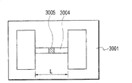
As the example that the element of this film conduction type radiated element constitutes, Figure 28 shows the planimetric map of the element that above-mentioned M.Hartwell etc. proposes.Among the figure, the 3001st, substrate, the 3004th, the conductive membrane of the metal acidulants that forms by sputter.Conductive membrane 3004 forms the flat shape of diagram H font.Be called the energising processing that energising is shaped by this conductive membrane 3004 is implemented aftermentioned, form electron emission part 3005.Interval L among the figure is made as 0.5~1 (mm), and W is made as 0.1 (mm).In addition, be simplicity of illustration, electron emission part 3005 illustrates with rectangular shape in the central authorities of conductive membrane 3004, but this is the pattern problem, not the position and the shape of the electron emission part of performance reality verily.
Headed by the element of M.Hartwell, in above-mentioned surface conductive type radiated element, before carrying out electronics emission, handle and form electron emission part 3005 by on conductive membrane 3004, implementing to be called energising that energising is shaped usually.Promptly; it is to apply certain DC voltage or for example ratio very slowly of the 1V/ branch degree DC voltage and the energising of boosting at the two ends of conductive membrane 3004 that energising is shaped; make conductive membrane 3004 local failures, distortion or rotten, form the electron emission part 3005 of high resistance state.In addition, the part at local failure, distortion or rotten conductive membrane 3004 chaps.When applying suitable voltage after above-mentioned energising is shaped, for conductive membrane 3004, near above-mentioned be full of cracks, carry out the electronics emission.
As the example of FE type, for example W.P.Dy
kE﹠amp; W.w.Dolan, Fieldemission, Advancein Electron Physics, 8,89 (1956) or C.A.Spindt, Physicalpropertiesofthin-filmfieldemissioncathodeswithmo lybdenumcones, J.Appl.Phys., 47,5248 (1976) etc. is known.
As the exemplary that the element of FE type constitutes, figure 29 illustrates the sectional drawing of the element that above-mentioned C.A.Spindt proposes.Among the figure, the 3010th, substrate, the 3011st, the emission wiring of conductive material, the 3012nd, emission cone, the 3013rd, insulation course, the 3014th, gate electrode.This element causes electric field transmitted by apply appropriate voltage between emission cone 3012 and grid 3014 at the leading section of launching cone 3012.Other element as the FE type constitutes, and is not stepped construction shown in Figure 29 but disposes the example of emitter and grid with base plan almost parallel ground on substrate.
As the example of mim type, C.A.Mead for example, Operationoftunnel-emissionDevices, J.Appl.Phys., 32,646 (1961) etc. is known.The exemplary that the element of mim type constitutes as shown in figure 30.Figure is a sectional drawing, among the figure, and the 3020th, substrate, the 3021st, the bottom electrode that metal makes, the 3022nd, the thin dielectric layer of thick 100 dust degree, the 3023rd, the top electrode that the metal of thick 80~300 dust degree makes.In mim type,, cause the electronics emission on top electrode 3023 surfaces by between top electrode 3023 and bottom electrode 3021, applying suitable voltage.
Above-mentioned cold cathode element and the comparison of hot cathode element can realize the electronics emission at low temperatures, therefore, do not need heater.But specific heat cathode element simple structure can make fine element.Even on substrate, dispose majority element to high-density, also be difficult to take place problems such as substrate heat fusion.To move by the heating of well heater with hot cathode and to make response speed different slowly, under the situation of cold cathode element, have the fast advantage of response speed.
Therefore, the research of application cold cathode element is very in vogue.
For example, surface conductive type radiated element since in cold cathode element inside because of simple in structure and easy manufacturing, therefore have the advantage that can in large tracts of land, form a plurality of elements.Here, for example, as the applicant the spy open in the clear 64-31332 communique disclosed, the method that is used to set and drive a plurality of elements is studied.
In the application of surface conductive type radiated element, studying the image processing system of for example image display device, image recording structure etc. and electric charge beam source etc.
Especially, as application towards image display device, USP5 for example, 066,883 and the flat 2-257551 communique of Te Kai and spy to open flat 4-2811373 communique disclosed like that, studied surface conductive type radiated element and the image display device that combines and use by the irradiation luminous fluorophor of electron beam.Wish that image display device that surface conductive type radiated element and fluorophor are used in combination has the image display device superior characteristic than existing other modes.For example, even and the liquid crystal indicator of popularizing in recent years relatively, we can say to have does not need the wide advantage of back light and visual angle because of autoluminescence.
USP4 more for example discloses a plurality of FE type arranged side by side and method of driving in 904,895.As the FE type is applied in example in the image display device, for example the planar display of proposition such as R.Meyer is known (R.Meyer:RecentDevelopmentonMicrotipsDisplayatLETI, Tech.Digestof4thInt.VacuumMicroelectronicsConf., Nb No. ≠. ≠ height=Cpp.6~9 (1991)).
For example open and disclose a plurality of mim types arranged side by side in the flat 3-55738 communique and be applied in example in the image display device the spy.
Further, as the image display device that uses electronic emission element element in addition, open the device that discloses use EL (electroluminescence) element in the flat 09-281928 communique for example spy.
The inventor attempts multiple electron beam source by electric wiring method for example shown in Figure 31.That is, a plurality of electronic emission elements of 2 dimension ground assortments, these elements are multiple electron beam sources of rectangular wiring as shown in the figure.
Among the figure, the 1st, the electronic emission element shown in the model, the 2nd, line direction wiring, the 3rd, column direction wiring.Line direction wiring 2 and column direction wiring 3 have cloth line resistance 4,5, wiring inductance 6,7 and wiring capacitance 8.Be simplicity of illustration, illustrate with the 4*4 matrix that certainly the size of matrix is not only limited to this, for example under the situation of the multiple electron beam source of device used for image display, but assortment is enough to element and the wiring of expecting that image shows.
For the multiple electron beam source of matrix wiring electronic emission element, the electron beam for output is wished applies suitable electric signal in line direction wiring and column direction wiring.
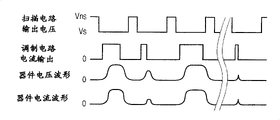
Figure 32 shows the pulse amplitude modulation waveform.For example, apply selection current potential Vs, apply non-selection current potential Vns for simultaneously the line direction wiring of non-selected row for driving any 1 electronic emission element of going in the matrix, give the line direction wiring of selecting row.Apply the driving current potential Ve that is used to export electron beam to the column direction wiring synchronously therewith.According to this method, apply the voltage of Ve-Vs to the electronic emission element of selecting row, apply the voltage of Ve-Vns to the electronic emission element of non-selection row.If Ve, Vs, Vn are made as suitable size, then only export the electron beam of wishing intensity from the electronic emission element of the row selected.Because the response speed of cold cathode element is fast, apply the time span that drives current potential Ve if change, the time span of then exporting electron beam also can change.
Similarly, imposing on the current potential and the current value of column direction wiring by said change and control the peak value modulation system of brightness also can controlling electron beam.
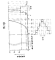
But valid pixel is counted in the display device of 1920*1080, frame rate 60Hz, 10 gray shade scales, under the situation of peak value of pulse modulator approach, when the energy peak that applies to element is Pi, needs Pi/2
10The decomposition energy of=Pi/1024.The situation Pi of driven is a number V degree, therefore requires drive waveforms that the decomposition energy of several mV is arranged on the 1920*1080 whole image.This value is difficult to realize when the characteristic of the IC that considers the formation driving circuit and printed base plate, power supply etc.
On the other hand, during the pulse amplitude modulation mode, the time that drives 1 sweep trace is 1/ (60*1080)
 15 μ sec.When carrying out 10 digit pulse amplitude modulation, the minimum pulse amplitude is 1/ (60*1080*2
10)
15 μ sec.When carrying out 10 digit pulse amplitude modulation, the minimum pulse amplitude is 1/ (60*1080*2
10)
 15nsec, the pulse amplitude resolution of minimum 15 nanoseconds of needs.
But, wiring shown in Figure 31 and the low-pass filter equivalence that has by the cutoff frequency of wiring inductance (L), wiring capacitance (C) and cloth line resistance (R) decision.Has the wiring of the signal routing of this low-pass characteristic and display part by with the spectrum structure more than the cutoff frequency, when line sequential pulse width modulated (PWM) type of drive drives, as shown in figure 33, be applied to the rising edge and the negative edge waveform rust of the PWM waveform on the element, produce display quality during low-light level and descend.Especially, when applying the pulse amplitude modulation drive waveforms of low gray shade scale from information electrode drive circuit 10 and the synthetic waveform of output waveform that imposes on the sweep circuit 11 of electronics mode element 1 become the waveform of peak value step-down.In a word, only, promptly hang down the peak value step-down of the pulse amplitude modulation drive waveforms of gray shade scale, in low gray shade scale zone, can not show the image of the gray shade scale of hope by the drive waveforms of high frequency spectrum components structure.
For a plurality of electron sources of much more very electronic emission elements of matrix wiring, providing under the situation of long short continuous current pulse of time by the control constant current supply, hardly emitting electrons.Continuing to provide under the situation of long time continuous current pulse, much less, the beginning emitting electrons, but until electronics emission beginning, the big rising edge time is necessary.
Figure 33 is the time diagram that is used to illustrate this, as shown in the figure, even supply with short current impulse by the control constant current supply, but flows through electric current I f hardly in electronic emission element.Even supply with the situation of long pulse, the drive current If that flows in electronic emission element becomes big waveform of rising edge time.Although the cold cathode type electronic emission element self has high speed response property, supply with the current waveform rust of electronic emission element, therefore, the waveform of final transmitter current Ie also is out of shape.
In a plurality of electron sources of simple matrix wiring, when the size of matrix was big, its stray capacitance (wiring capacitance) increased.The major part of stray capacitance is positioned at the cross part of line direction wiring and column direction wiring, and Figure 34 shows this equivalence circuit.When the control constant current supply 9 that connects column direction wiring 3 began to supply with continuous current I1, initial current expended in the charging of stray capacitance 8, acted on hardly as the drive current of electronic emission element 1.Therefore, the real response speed of electronic emission element is low.
The problem that should solve below in driven, existing.Make element that electric current flows through for example in the displays such as LED, EL, FED, SED using as light-emitting component to follow to drive, the resistive arrangement that generally connects up gets little.But the pattern shown in Figure 31 of stray capacitance, dead resistance, stray inductance structure is as equivalent circuit.In this circuit, when being suitable for existing driven method, by applying voltage, the charging current i of stray capacitance flows into, drive waveforms rising edge part rust.Further, the self-induction action by stray inductance produces electromotive force U=-L* (di/dt), produces emission, is coupled, and this causes to light-emitting component and applies abnormal voltage.
In recent years, along with large tracts of land, height requirement meticulous, high gray shade scale to display are more and more obvious, the stray inductance of wiring, stray capacitance increase, owing to the passivation of drive waveforms rising edge part makes gray shade scale passivation in the low brightness area, cross emission, coupling becomes important topic to be solved all the more.
Drive waveforms by control of simple pulse width and peak value of pulse control can not guarantee the monotone increasing of gray shade scale owing to the variation of the voltage/luminous intensity characteristic of light-emitting component and deviation.
For example, open in the flat 09-319327 communique disclosed such the spy, it is the voltage source that charges at a high speed by in Control current source from drive current to above-mentioned cold cathode element that supply with, to the family planning electric capacity of multiple electron source, the charging voltage bringing device that above-mentioned voltage source and above-mentioned column direction wiring be electrically connected synchronous with the rising edge of above-mentioned drive current, before wiring parasitic electric capacity charging was finished substantially, also execution applied the method etc. of charging voltage except that drive current.When carrying out this driving, can guarantee the linearity of gray shade scale.
Open in the flat 8-22261 communique the spy, each word of data image signal is divided into a plurality of sub-words, peak value is low in the word of following seat, by in the word of last seat, distribute the high PWM waveform of peak value to realize to have than before the drive waveforms during the long time slot during the time slot of PWM waveform, the image display quality is low when preventing low-light level.
Open in the flat 10-39825 communique the spy, by having the 2nd pulse amplitude modulation output unit of 2 value signals that corresponding brightness signal output HIGH voltage is V2 for the V1 low-voltage and corresponding above-mentioned luminance signal are cut above-mentioned 2 value signals the 2nd pulse amplitude signal output apparatus into the pulse width of regulation driving method, can reduce the frequency of pulse amplitude modulation circuit, solve the high-frequency problem of following high gray shade scale and becoming the PWM operating frequency of problem.
Further, open in the flat 11-015430 communique the spy, as potential pulse, comprise the pulsed drive waveform of the M*N gray shade scale information that the peak value of pulse control with control of the pulse width of corresponding M gray shade scale and corresponding N gray shade scale defines by use, realize high gray shade scaleization easily.
But when driving by existing pulse amplitude modulation, specifically, gray shade scale constantly can cause big electromagnetic wave noise or unnecessary electromagenetic wave radiation at the rising edge negative edge of drive waveforms.
A plurality of to above-mentioned electronic emission element, be in the multiple electron beam source of matrix configuration, because producing voltage, the influence of its wiring resistance descends, therefore the voltage that imposes on each element powers up end from it, and to begin element voltage far away more low more, consequently, still there is the emitting electrons of each element different problem that distributes.And, when should a plurality of electronic emission elements being applied in the image display device,, the cloth line resistance descends because producing voltage, therefore there is the problem of image quality variation.
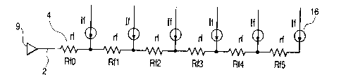
Describe with Figure 34 and Figure 35.Figure 34 shows a routine multiple electron beam source substrate.Among the figure, the 1st, electronic emission element, the 2nd, select electrode (line direction wiring), the 3rd, information electrode (column direction wiring), the 9th, select circuit, the 10th, modulation circuit, the 12nd, substrate.
Figure 35 is to use the skeleton view of image display panel of the multiple electron beam source substrate 11 of Figure 34.Among the figure, the 13rd, betal can, the 14th, video screen, the 15th, the fuse plate, the 16th, from the electric current of current source.
Now, select certain to select electrode 2, connect the whole pixels that are connected with this selection electrode.The equivalent circuit of this moment as shown in figure 36.Among the figure, the 16th, flow through the current component of selecting electrode from the information electrode by electronic emission element, the 4th, the resistive component of selection electrode.
Here, flowing into and selecting the electric current of electrode all is identical value If to each element, and the resistance value of supposing the selection electrode of each pixel is rf.Calculate the current potential of selecting this moment on the electrode.
The electric current that flows through Rf5 is If, and the voltage drop amount by Rf5 is Ifrf.The electric current that flows through Rf4 is 2If, and the voltage drop amount by R f4 is 2Ifrf.Below similarly calculate the voltage drop amount in each resistive component, calculate the current potential of selecting each several part on the electrode, the results are shown in Figure 37.In addition,, show the situation of Ve>Vs here.
It should be noted that when selecting circuit 9 output potential Vs as certain of electric-adding point, electric current flows into selects electrode 2, current potential rises during away from the electric-adding point, is that the current potential of 21Ifrf rises in distal-most end.Figure 38 shows the drive waveforms that is applied to this moment on the distal-most end pixel.(a) is applied to the potential waveform of selecting on the electrode among the figure, (b) is the potential waveform that is applied on the information electrode, (c) is the voltage waveform that is applied on the selected electronic emission element.Because current potential rises, select current potential to become Vs ' from Vs, the voltage that imposes on element descends.
This voltage deviation very hour does not have difference at the resistive component of selecting electrode and waits (は さ ほ ど) problem, but for example because the big picture of image display device etc., when the resistive component of selecting electrode was big, its voltage deviation can not be ignored.Pixel count increases, flows into when the electric current of selecting electrode increases also makes its voltage deviation become big.
Owing to produce this voltage deviation, the voltage that imposes on electronic emission element is different in each element, especially, and near electronic emission element the electric-adding point and the electronic emission element away from the electric-adding point, be not applied to identical voltage, aspect the emission measure of electronics, produce difference.This situation is brought by from its electronic emission element ejected electron bundle, shows as the luminance difference between the pixel of light-emitting component, and the display quality of image display device descends.
Open in the flat 10-112391 communique the spy and to disclose: pay close attention to the resistance value of cloth line electrode of X-Y matrix type organic EL display and the electric current that in the corresponding wiring line electrode, flows, data electrode is arranged in the wiring of low resistance side, scan electrode is arranged in the wiring of high resistance side, simultaneously, the driving method of the driven with current sources that is connected by voltage source with driving voltage Vcc, even the driving voltage Vcc of this moment is owing to the cloth line resistance that the position in pixel light emission element causes has deviation, current source must be more than the specific voltage that satisfies the continuous current operation condition yet, make a plurality of light-emitting component uniformly light-emittings, realize advantageous characteristic as image display device.
Put down in writing the negative edge that will be applied to the signal in the modulation wiring (information signal wiring) in No. 3049061 in special permission and be divided into the situation that a plurality of steps are carried out.
Open to have put down in writing in the flat 7-181917 communique the spy and use and the corresponding a plurality of voltages of single or multiple units drive block, on pulse amplitude and peak value direction, pile up the method that this unit drive block forms drive waveforms.
Summary of the invention
One of the invention of the driving circuit of the light-emitting component that the application relates to structure is as follows.The driving circuit of light-emitting component, luminous for making light-emitting component with the brightness corresponding with brightness data, by pressing A at least with peak value in time slot width Δ t unit gating pulse width and each time slot
1~A
n(wherein, n is the integer more than 2,0<A n stage
1<A
2<...<A
n) drive waveforms of carrying out peak value control drives above-mentioned light-emitting component, it is characterized in that having the regulation of rising to peak A
kWhole drive waveforms of the part of (wherein k is the following integers of 2 above n) are in order to from peak A
1To peak A
K-1Each peak value all experience a time slot at least, until rising to the afore mentioned rules peak A
k
According to the present invention, can correct driven light-emitting element by stage ground rising drive waveforms.And, in the rising edge of drive waveforms part, compare peak A having to rise to
kUnder the situation of also high peak value part, preferably arrive peak A
kAfter the drive waveforms that sharply do not rise.In foregoing invention, wish peak A
kIt is (rising edge part at least) peak-peak of drive waveforms.
The structure of one of invention of the driving circuit of the light-emitting component that the application relates to is as follows.The driving circuit of light-emitting component, luminous for making light-emitting component with the brightness corresponding with circuit data, by with time slot width Δ t be in unit gating pulse width and each time slot peak value at least by A
1~A
n(wherein, n is the integer more than 2,0<A n stage
1<A
2<...<A
n) drive waveforms of peak value control drives above-mentioned light-emitting component, it is characterized in that having from the regulation peak A
kWhole drive waveforms of (wherein k is the following integers of 2 above n) beginning sloping portion are from the afore mentioned rules peak A
kBeginning is in order to from peak A
K-1To peak A
1Every peak value all experience time slot ground at least and descend.The also correct driven light-emitting element according to the present invention.
The structure of one of invention of the driving circuit of the light-emitting component that the application relates to is as follows.The driving circuit of light-emitting component, luminous for making light-emitting component with the brightness corresponding with brightness data, by pressing A at least with peak value in time slot width Δ t unit gating pulse width and each time slot
1~A
n(wherein, n is the integer more than 2,0<A n stage
1<A
2<...<A
n) in carry out peak value control drive waveforms drive above-mentioned light-emitting component, it is characterized in that above-mentioned drive waveforms has in order from peak A
1To peak A
K-1Each peak value when all experiencing one at least the unoccupied place until rising to the regulation peak A
kThe part of (wherein k is the following integers of 2 above n) and in order to from above-mentioned peak A
K-1To peak A
1Each peak value all experience the part that time slot ground descends at least.
(following description the 3rd driving method)
Correct driven light-emitting element when using the driving circuit of putting down in writing among the present invention.
In above-mentioned each invention, in the rising edge part of drive waveforms, rise to peak A in addition
1The peak value that is right after before is that light-emitting component in fact can not driven peak value.In the negative edge part of drive waveforms, from peak A
1The peak value that is right after after beginning to descend is the not driven in fact peak value of light-emitting component.Here, even being this peak value, the not driven in fact peak value of light-emitting component do not made light-emitting component produce the luminous peak value corresponding with the minimum gray shade scale of brightness data by 1 time slot input yet, specifically, this peak value should be hanked and be no more than the drive threshold of light-emitting component.
Consideration provides the state of rheobase when aftermentioned matrix driving (for example selection current potential) to light-emitting component.When the invention that relates to by the application provided drive waveforms for this light-emitting component, the current potential that will be corresponding with the each several part of drive waveforms (this current potential is the current potential that when carrying out peak value control by Current Control this electric current is flowed when carrying out peak value control by control of Electric potentials) and the potential difference (PD) of above-mentioned rheobase offered light-emitting component.Peak value when producing can not ignore luminous by this potential difference (PD) when showing according to brightness data is the drive threshold of light-emitting component.
In addition, can adopt this drive waveforms rising to A
1The not driven in fact peak value of light-emitting component before and from A
1The identical structure of the not driven in fact peak value of light-emitting component after beginning to descend.Here, the size of mentioning peak value is to point to the peak value that light-emitting component provides big (height) peak value and more driving energy when (just), and not necessarily the magnitude relationship with current potential is consistent.For example, provide the regulation current potential, when the current potential of drive waveforms is compared drive waveforms with it and is electronegative potential, become low but the state that peak value is high of current potential as rheobase.
In above structure, make the relation of other drive waveforms of the driving energy increase and decrease of driven light-emitting element by following certain drive waveforms and this drive waveforms stipulated, can suitably set drive waveforms.That is, above-mentioned drive waveforms is risen to peak A
1Time slot during as the 1st time slot, be respectively A for the peak value of the 1st~the k-1 time slot
1~A
K-1, k and N
k+ k-1 time slot (N wherein
kBe integer greater than 1) peak value be A
k, N
k+ k~N
kThe peak value of+2 (k-1) time slot is respectively A
K-1~A
1Drive waveforms, the drive waveforms that makes the driving energy that drives above-mentioned light-emitting component increase by 1 grade is the N that makes above-mentioned drive waveforms
kThe peak value of+2k-1 time slot is increased to A
1Waveform, later on the order drive waveforms that makes above-mentioned driving energy increase by 1 grade has N for the drive waveforms of prime
kThe peak value of+2 (k-1) time slot is from A
1Change to A
2..., with N
kThe peak value of+k time slot is from A
K-1Change to A
kWaveform.
That is, to having from peak A
kBeginning contrasts peak A in order
kEach low peak value all experiences a time slot ground and drops to the in fact drive waveforms of the part of driven peak value not of above-mentioned light-emitting component, and the drive waveforms that makes the energy that drives above-mentioned light-emitting component increase by 1 grade has in the above-mentioned sloping portion of prime drive waveforms makes then that peak value is A
1The peak value of time slot of time slot be increased to A
1Waveform, increase to drive later 1 grade by 1 grade the drive waveforms of above-mentioned light-emitting component energy, in the prime drive waveforms, prime drive waveforms is again had the peak value that peak value is increased before 1 grade the time slot increases by 1 grade waveform again.
In addition, invention described here is the invention that comprises such embodiment: the regulation drive signal waveform, to being equivalent to the 1st drive waveforms of certain gray shade scale energy, increase by 1 grade of the 2nd drive waveforms when driving energy and be under according to situation of the present invention, in certain specified time limit, do not limit the application time of the 1st and the 2nd drive waveforms, for example the time with the 1st drive waveforms, during rise the structure of the 1st drive waveforms since the 2nd time slot of specified time limit, with the 2nd drive waveforms the time, the initial time slot of the 2nd drive waveforms during the afore mentioned rules begins to rise.That is embodiments of the invention rising edge time of being not limited to rising edge time of the 1st drive waveforms and the 2nd drive waveforms same structure in specified time limit (for example during 1 selection during the aftermentioned matrix driving).
Above-mentioned each invention can be as described below.That is, driving method is characterised in that, for having from peak A
kBeginning contrasts peak A in order
kThe part that low each peak value descends is all at least through the regulation drive waveforms of a time slot, increases by 1 grade of drive waveforms that drives the energy of above-mentioned light-emitting component and has in the part of the above-mentioned decline of prime drive waveforms and make that to follow peak value be A
1The time slot peak value of time slot be increased to A
1Waveform, later one-level one-level increases the drive waveforms that above-mentioned light-emitting component drives energy, in the prime drive waveforms, has the waveform that the peak value that will the peak value of prime drive waveforms again be increased the time slot before the time slot of one-level increases one-level again.
By the relation of each drive waveforms of setting like this, can be in the continuous time slot in the negative edge part of each drive waveforms at 1 grade with the interior peak change of carrying out.
Especially, be suitable for adopting this structure: for the prime drive waveforms, one-level one-level ground increases the drive waveforms of the energy that drives above-mentioned light-emitting component, in the prime drive waveforms, having increases peak value the above-mentioned relation that peak value before the time slot of one-level increases the waveform of one-level again to prime drive waveforms again, and the peak value of time slot that makes the peak value increase according to the drive waveforms of this relation decision for the prime drive waveforms is than peak A
kAlso a succession of drive waveforms is met before the drive waveforms of higher leveled peak value.The drive waveforms that the last waveform of these a succession of drive waveforms is also increased one-level driving energy can have such waveform: in the negative edge part of above-mentioned last drive waveforms, it is A that peak value will be followed peak value
1The time slot peak value of time slot become A
1
Peak A
kBe the peak-peak of allowing, avoiding peak value more under the news as far as possible, can be as described below.Promptly, can be this structure: to the prime drive waveforms, the one-level one-level increases the drive waveforms of the energy that drives above-mentioned light-emitting component, in the prime drive waveforms, prime drive waveforms again had making peak value increase the above-mentioned relation that time slot peak value before the time slot of one-level increases the waveform of one-level again, is that to make the peak value of the time slot of peak value increase for the prime drive waveforms be A at peak value by the drive waveforms of this relation decision
kDrive waveforms before a succession of drive waveforms be met.Increasing drive waveforms that one-level drives energy again for drive waveforms last in these a succession of drive waveforms is that to have then peak value be A for peak value in above-mentioned last drive waveforms negative edge part
1The peak value of time slot of time slot become A
1Waveform.
Each grade drives the different a succession of drive waveforms of energy and can followingly set.That is, structure is: above-mentioned drive waveforms is risen to peak A
1After time slot during as the 1st time slot, be respectively A for the peak value of the 1st~the k-1 time slot
1~A
K-1, k and N
k+ k-1 time slot (N wherein
kBe integer greater than 1) peak value be A
k, N
k+ k~N
kThe peak value of+2 (k-1) time slot is respectively A
K-1~A
1Drive waveforms, the drive waveforms that makes the driving energy that drives above-mentioned light-emitting component reduce 1 grade is to make the peak value of k time slot of above-mentioned drive waveforms from A
kBecome A
K-1Waveform, it is as follows that later on order reduces the waveform configuration of drive waveforms of 1 grade of above-mentioned driving energy: for the drive waveforms of prime, the peak value that is the k-1 time slot specifically is from A
K-1Become A
K-2..., the peak value of the 1st time slot is from A
1Become the not driven in fact peak value of above-mentioned light-emitting component.
In addition, invention described here is the invention that comprises such embodiment: the regulation drive signal waveform, to being equivalent to the 1st drive waveforms of certain gray shade scale energy, when reducing by 1 grade of the 2nd drive waveforms when driving energy and be according to situation of the present invention, in certain specified time limit, do not limit the application time of the 1st and the 2nd drive waveforms, for example the time with the 1st drive waveforms, in the initial time slot since specified time limit rises the structure of the 1st drive waveforms, with the 2nd drive waveforms the time, the embodiment that 2nd time slot of the 2nd drive waveforms during the afore mentioned rules begins to rise.That is, embodiments of the invention negative edge time of being not limited to negative edge time of the 1st drive waveforms and the 2nd drive waveforms is identical in specified time limit (for example during 1 selection during the aftermentioned matrix driving).
Can have following situation.That is, structure is characterised in that, for having at least one time-slot sequence process than peak A
kEach low peak value and drop to peak A
kThe drive waveforms of part, reduce by 1 grade of drive waveforms that drives the energy of above-mentioned light-emitting component and have in the above-mentioned rising part of prime drive waveforms that to make as then peak value be A
K-1The time slot peak value of time slot be A
kThe peak value of time slot become A
K-1Waveform, later one-level one-level reduces the drive waveforms of the energy that drives above-mentioned light-emitting component, in the prime drive waveforms, prime drive waveforms is again had the waveform that the peak value that makes peak value reduce the time slot before the time slot of one-level reduces one-level again.
In above-mentioned each invention, be A at peak value
k2 time slots between time slot in, peak value is A preferably
kKeep peak value at rising edge and negative edge with external enwergy, therefore driven light-emitting element more correctly, drive waveforms also generates easily.
Best following the setting.That is, architectural feature is, is A at above-mentioned peak value
k2 time slots between when another time slot is arranged, peak value is A in this another time slot
k, comprise the above-mentioned peak A of k=1
kCompare A
nAlso little, and for the drive waveforms of prime, drive energy and increase one-level by making, be A for peak value
kTimeslot number from 2 this drive waveforms that become 3, further increasing drive waveforms that one-level drives energy, to have above-mentioned drive waveforms peak value be A
k3 time slots in the middle of the peak value of time slot from A
kBecome A
K+1Shape.
The drive waveforms of comparing the driving energy increase that makes the above-mentioned light-emitting component of driving with the regulation drive waveforms preferably has with making the peak-peak rising the afore mentioned rules drive waveforms compares the shape that pulse width is increased.
When increase driving energy, compare preferential increase pulse width with the rising of peak value, can obtain reducing the effect of the electric current that transient flow crosses.Here, compare with the peak value rising, structure when being fit to preferentially increase pulse width is: rise or the decline shape on one side at least one time slot ground, one side is kept through each peak value, when driving energy by the pulse width increase of extending some peak values, do not make the peak-peak rising.
It is suitable carrying out following setting.That is the structure of the drive waveforms when, the drive waveforms of regulation being increased one-level and drives the driving energy of above-mentioned light-emitting component and improve the peak-peak of drive waveforms is: by peak difference A
n-A
N-1... or A
2-A
1Perhaps peak A
1Comparing with the number that uses in the afore mentioned rules drive waveforms with the unit drive waveforms piece number that peak difference and time slot width Δ t as the peak value of above-mentioned light-emitting component drive threshold determines increases by one, has stack so that peak-peak continuous shape as far as possible.
When increase driving energy, compare with the rising of peak value, by preferential increase pulse width, can obtain reducing the effect of the electric current that transient flow crosses.But, increasing in the structure of pulse width in order to increase the driving energy, when the pulse width of drive waveforms is restricted, in the level of regulation, need to use peak value than higher.Pay attention to peak value particularly under the successional situation of peak-peak, rise or the level shape descends or aspect two all fully in the scope, can make the unit drive waveforms piece that constitutes drive waveforms become the upright shape of stack so that peak-peak is continuous as far as possible at the level shape.
It is suitable carrying out following setting.That is, to the drive waveforms of regulation, the structure that increases the drive waveforms of the driving energy that drives above-mentioned light-emitting component is: by peak difference A
n-A
N-1... or A
2-A
1Perhaps peak A
1With as the peak difference of the peak value of above-mentioned light-emitting component drive threshold and the unit drive waveforms piece of time slot width Δ t decision, comprise the peak-peak A of k=1
kOn lower position, has preferential additional shape.Especially, to the drive waveforms of regulation, increase to drive above-mentioned light-emitting component the driving energy drive waveforms structure preferably: by peak difference A
n-A
N-1... or A
2-A
1Perhaps peak A
1With as the peak difference of the peak value of above-mentioned light-emitting component drive threshold and the unit drive waveforms piece of time slot width Δ t decision, have preferential additional shape on and the position that peak-peak is continuous lower in peak-peak.
Specifically, maximum timeslot number is S, is A to peak-peak
kTimeslot number become the drive waveforms of S-2 (k-1), the drive waveforms that makes above-mentioned driving energy further increase by 1 grade by additional above-mentioned unit drive waveforms piece is to have in k+1~S-k time slot arbitrarily the peak value of time slot from A
kBecome A
K+1The drive waveforms of shape.Peak value is from A
kBecome A
K+1Time slot for example can be any one in k+1 or the S-k time slot for example.
The present invention: to the drive waveforms of regulation, drive waveforms when increasing one-level and drive the driving energy of above-mentioned light-emitting component and improve the peak-peak of drive waveforms, comprise that above-mentioned unit drive waveforms piece number also increases by one than the number that uses in the drive waveforms of afore mentioned rules, have the upright shape of stack so that peak-peak has continuous as far as possible structure; Comprise the peak-peak A of k=1 with above-mentioned unit drive waveforms piece
kThe structure of centre that on lower position, has the structure of preferential additional shape.Promptly, drive waveforms to regulation, drive waveforms when increasing one-level and driving the driving energy of above-mentioned light-emitting component and improve the peak-peak of drive waveforms, above-mentioned unit drive waveforms piece number also increases by one than the number that uses in the drive waveforms of afore mentioned rules, have the upright shape of stack so that continuous 2 more than the time slot of peak-peak.
Further, the present invention comprises the above discontinuous structure of peak-peak of 2 time slots.Promptly, drive waveforms to regulation, drive waveforms when increasing one-level and driving the driving energy of above-mentioned light-emitting component and improve the peak-peak of drive waveforms, above-mentioned unit drive waveforms piece number also increases by one than the number that uses in the drive waveforms of afore mentioned rules, have the upright shape of stack so that peak-peak becomes 2 more than the time slot.
In above each invention, peak value is A
1Time slot width be that the drive waveforms of Δ t preferably makes to have and makes above-mentioned light-emitting component with the luminous driving energy of the brightness of about 1LSB of corresponding brightness data.
Above-mentioned peak A
1~A
nSuitable employing has the structure of different potentials value respectively, for example, and above-mentioned peak A
1~A
nCan adopt the brightness of above-mentioned light-emitting component to have about 1: 2: ...: the structure of the current potential of n.Above-mentioned peak A
1~A
nAdopt peak difference A
m-A
M-1(wherein m is the following integer of 1 above n, and A0 is the drive threshold of light-emitting component) has the structure of certain approximately current potential.Above-mentioned peak A
1~A
nAdopt and have the structure of different current values respectively.
The structure that can adopt is characterised in that peak difference A
m-A
M-1(wherein m is the following integer of 1 above n, and A0 is the drive threshold of light-emitting component) is certain basically, is A for the m more than 2 perhaps
m-A
M-1〉=A
M-1-A
M-2, comprise the situation of k=1, above-mentioned peak A
kBecome the peak-peak and the above-mentioned peak A of drive waveforms
kCompare A
nLittle, and to be clipped in above-mentioned peak value be A
kTime slot in the time slot peak value be A
k, to above-mentioned N
k+ 2 (k-1) reach the drive waveforms of the maximum timeslot number S (wherein S is the above integer of 2n-1) of regulation, make under the situation of 1 grade of the further increase of above-mentioned driving energy, replace becoming A in abutting connection with peak value
1Time slot and the peak value peak value that becomes the time slot of the peak value that above-mentioned light-emitting component do not drive by essence become A
1, peakedness ratio A
1Also high timeslot number (Sk+2k+1)/(k+1) is above from its nearest integer, and peak-peak is A
K+1, by above-mentioned peak difference A
m-A
M-1The unit drive waveforms piece number of determining with time slot width Δ t only is being changed to drive waveforms in many 1 above-mentioned the 3rd driving method to above-mentioned drive waveforms, and peak value is A
1~A
kIn any, identical time slot is a plurality of situation, when further increasing by 1 grade of above-mentioned driving energy afterwards, peakedness ratio is less, is that the peak value of time slot increased 1 grade near time slot more than 1 grade made by peak value.
According to this structure, above-mentioned peak A
1~A
nBrightness with above-mentioned light-emitting component is about 1: 2: ...: the structure of the current potential of n, above-mentioned peak A
1~A
nCan adopt peak difference A
m-A
M-1(wherein m is the following integer of 1 above n, and A0 is the drive threshold of light-emitting component) is the formation of approximately certain current potential.Above-mentioned peak A
1~A
nCan adopt peak value to be about 1: 2: ...: the structure of the current value of n.
The application comprises following invention.Promptly, produce driving circuit with the corresponding drive waveforms of brightness level data, it is characterized in that, produce the drive waveforms that the discontinuous a plurality of peak values of non-minimum peak more than 1 with the peak value of the minimum peak that comprises corresponding peak value as non-0 above-mentioned brightness level data and corresponding big as a comparison above-mentioned brightness level data carry out peak value control, carry out pulse width control with discontinuous pulse width; Above-mentioned drive waveforms with part that above-mentioned non-minimum peak is controlled is the waveform that has the part that is controlled to above-mentioned minimum peak at the beginning of this drive waveforms and end.
Here, the peak value of corresponding non-0 brightness level data be said can produce by the drive waveforms that applies this peak value of control to light-emitting component with 0 beyond the corresponding luminous peak value of brightness level data.
The application comprises following invention.Promptly, produce driving circuit with the corresponding drive waveforms of brightness level data, it is characterized in that, produce the drive waveforms that the discontinuous a plurality of peak values of non-minimum peak more than 1 with the peak value of the minimum peak that comprises corresponding peak value as non-0 above-mentioned brightness level data and corresponding big as a comparison above-mentioned brightness level data carry out peak value control, carry out pulse width control with discontinuous pulse width; Whole above-mentioned drive waveforms with part that above-mentioned non-minimum peak is controlled is the waveform that has the part that is controlled to above-mentioned minimum peak in one of them at the beginning of this drive waveforms or end.
The application comprises following invention.Promptly, produce driving circuit with the corresponding drive waveforms of brightness level data, it is characterized in that, produce discontinuous a plurality of peak values with the non-minimum peak of the peak value of the minimum peak that comprises corresponding peak value as non-0 above-mentioned brightness level data and corresponding big as a comparison above-mentioned brightness level data and middle the peak value between above-mentioned minimum peak and the non-minimum peak and carry out peak value and control, carry out the drive waveforms that pulse width is controlled with discontinuous pulse width; As above-mentioned drive waveforms with the part that is controlled to above-mentioned non-minimum peak, have its beginning be controlled to the stipulated time width above-mentioned minimum peak part and mask thereafter have be controlled to above-mentioned in the middle of the part of peak value, after this, produce the drive waveforms that has the part that is controlled to the above-mentioned non-minimum peak bigger with the width bigger than peak value in the middle of above-mentioned than the time width of afore mentioned rules.
Middle peak value is preferably more than 2.
The application comprises following invention.Promptly, produce driving circuit with the corresponding drive waveforms of brightness level data, it is characterized in that, produce to comprise as the minimum peak of the peak value of the above-mentioned brightness level data of correspondence non-0 and to carry out peak value as discontinuous a plurality of peak values of the non-minimum peak of the peak value of the bigger above-mentioned brightness level data of correspondence and middle the peak value between above-mentioned minimum peak and the above-mentioned non-minimum peak and control, carry out the drive waveforms that pulse width is controlled with discontinuous pulse width; As above-mentioned drive waveforms with the part that is controlled to above-mentioned non-minimum peak, have be controlled to the part of above-mentioned minimum peak at its end and after it, be controlled to above-mentioned in the middle of the part of peak value, produce with the width bigger than the time width of afore mentioned rules have be controlled to above-mentioned in the middle of before the part of peak value control ratio above-mentioned in the middle of the drive waveforms of part of the big above-mentioned non-minimum peak of peak value.
The application comprises following invention.That is, driving method is for making light-emitting component with luminous with the corresponding brightness of brightness data, by carrying out in pulse width control and each time slot peak value with time slot width Δ t unit at least by A
1~A
nN the level (wherein, n is the integer more than 2,0<A
1<A
2<...<A
n) drive waveforms of carrying out peak value control drives above-mentioned light-emitting component, it is characterized in that, to having in order from peak A
kBegin to than peak A
kThe regulation drive waveforms of the part that each low peak value all descends through time slot ground at least increases drive waveforms that one-level drives the energy of above-mentioned light-emitting component and is that to connect peak value in the above-mentioned negative edge part with the prime drive waveforms be A
1The time slot peak value of time slot be increased to A
1Waveform, afterwards, one-level one-level ground increases the drive waveforms of the driving energy that drives above-mentioned light-emitting component in the prime drive waveforms, to prime drive waveforms again, from as selecting the drive waveforms of wanting and drive above-mentioned light-emitting component a succession of drive waveforms of waveform that makes peak value increase time slot peak value before the time slot of one-level to increase again one-level.
Above-mentioned a succession of drive waveforms for example is that the drive waveforms from afore mentioned rules begins to the drive waveforms of the next stage of this regulation drive waveforms, promptly in the above-mentioned negative edge part of this regulation drive waveforms, makes that to connect peak value be A
1The time slot peak value of time slot be increased to A
1Drive waveforms and after it according to the drive waveforms of the said energy that prime drive waveforms one-level one-level increase is driven above-mentioned light-emitting component in the prime drive waveforms, to prime drive waveforms again have make peak value increase time slot peak value before the time slot of one-level increase again one-level waveform the above-mentioned relation decision 1 above drive waveforms and, according to this relation, it is peak A that the prime drive waveforms is made the peak value of the time slot of peak value increase
kA plurality of drive waveforms of drive waveforms.
Above-mentioned a succession of drive waveforms is to be peak A according to above-mentioned relation to the time slot peak value that the prime drive waveforms increases peak value
kThe drive waveforms of subordinate of drive waveforms, according to above-mentioned relation, can have peak value in the prime drive waveforms is A
kA time slot before the time slot peak value become and compare A
kThe a succession of drive waveforms before the drive waveforms of higher leveled peak value also perhaps, according to above-mentioned relation, to the prime drive waveforms, is a peak A at the peak value of the time slot that peak value is increased
kThe negative edge part of above-mentioned drive waveforms in, can have the peak value of connection is A
1The peak value of time slot of time slot be increased to A
1Waveform.
The application comprises following invention.That is, driving method is for making light-emitting component with luminous with the corresponding brightness of brightness data, by carrying out in pulse width control and each time slot peak value with time slot width Δ t unit at least by A
1~A
nN the level (wherein, n is the integer more than 2,0<A
1<A
2<...<A
n) drive waveforms of carrying out peak value control drives above-mentioned light-emitting component, it is characterized in that, contrasts peak A in order to having
kThe regulation drive waveforms of the part that each low peak value all rises through time slot ground at least reduces drive waveforms that one-level drives the energy of above-mentioned light-emitting component and is that to have the peak value of connection in the above-mentioned rising edge part of prime drive waveforms be A
K-1The time slot peak value of time slot be A
kThe time slot peak value be A
K-1Waveform, afterwards the one-level one-level reduce to drive above-mentioned light-emitting component the drive waveforms of energy in the prime drive waveforms, from selecting the drive waveforms of wanting and drive above-mentioned light-emitting component as prime drive waveforms again being made peak value reduce a succession of drive waveforms of waveform that time slot peak value before the time slot of one-level reduces one-level again.
The application comprises following invention.That is, driving method is for making light-emitting component with luminous with the corresponding brightness of brightness data, by carrying out in pulse width control and each time slot peak value with time slot width Δ t unit at least by A
1~A
nN the level (wherein, n is the integer more than 3,0<A
1<A
2<...<A
n) drive waveforms of carrying out peak value control drives above-mentioned light-emitting component, it is characterized in that a plurality of drive waveforms of corresponding a plurality of above-mentioned brightness datas are to have the regulation of rising to peak A
kThe drive waveforms of the part of (wherein k is the following integers of 3 above n), and, comprise and have in order from peak A
1To peak A
K-1Each peak value all at least through a time slot rise to the afore mentioned rules peak A
kThe drive waveforms of part.
The application comprises following invention.That is, driving method is for making light-emitting component with luminous with the corresponding brightness of brightness data, by width Delta t unit in crack is carried out in pulse width control and each time slot peak value at least by A
1~A
nN the level (wherein, n is the integer more than 3,0<A
1<A
2<...<A
n) drive waveforms of carrying out peak value control drives above-mentioned light-emitting component, it is characterized in that a plurality of drive waveforms of corresponding a plurality of above-mentioned brightness datas are to have from the regulation peak A
kThe drive waveforms of (wherein k is the following integers of 3 above n) beginning sloping portion, and, comprise and have the afore mentioned rules of fading peak A
kBegin time-slot sequence of at least one time slot through the peak A of associating
K-1To peak A
1Each peak value and the drive waveforms of sloping portion.
In above-mentioned each invention, above-mentioned light-emitting component is to constitute a plurality of light-emitting components that matrix shows, can suitably adopt and apply the structure of the above-mentioned drive waveforms of the brightness data corresponding with it for respectively each light-emitting component.
The present invention comprises the invention of following structure as the invention of display device.
Display device has: multiple optical element, use wiring of scanning signal lines and information signal and a plurality of light-emitting components of matrix wiring; Sweep circuit is connected with the said scanning signals wiring; Modulation circuit is connected with above-mentioned information signal wiring; It is characterized in that above-mentioned modulation circuit drives the light-emitting component of selecting by above-mentioned sweep circuit with the driving method of above-mentioned each invention.
Specifically, each scanning signal lines of sweep circuit select progressively, to offer the scanning signal lines of selecting as the selection current potential of regulation basis current potential, in a plurality of light-emitting components that connect this scanning signal lines of selecting, a plurality of information signal wirings that connect by them provide the signal with above-mentioned drive waveforms.
In this structure, when the rising edge of above-mentioned drive waveforms begins to arriving peak-peak A
kTime preferably set for to approximate and grow by 0%~90% time constant of the driving force decision of the load of the information signal of above-mentioned multiple optical element wiring and above-mentioned driving circuit or than it.
0%~90% time constant is the time constant of energy measurement in the part that drive waveforms is provided to wiring, be drive waveforms when rising to expectancy wave, the current potential in this part reached from 0.9 times of needed time of current potential of the potential difference (PD) that begins to change to expectancy wave.Than approximating or in also long time,, can applying the voltage more than 90% of the voltage that should impose on the electron source two ends, can obtain expecting the brightness more than 90% of luminous quantity by the rising drive waveforms greater than 0%~90% time constant.
As the structure that can be dispersed in the electric current that flows simultaneously of flowing in the wiring of a plurality of information signals, be suitable for adopting drive waveforms in a part of information signal wiring that is applied in above-mentioned a plurality of information signal wiring to be controlled to be rising edge and be controlled to be the structure of negative edge for the latter half during selecting for the first half during selecting, the drive waveforms that is applied in the information signal wiring of another part.During a selection, set a plurality of time slots that are used for pulse width control.Specifically, be applied to the drive waveforms in a part of information signal wiring in a plurality of information signal wirings, no matter corresponding driving energy (gray shade scale) how, all during selecting, be applied to from initial (perhaps its next door) time slot that is used for pulse width control and begin to rise, impose on the drive waveforms of remaining information signal wiring, no matter corresponding driving energy how, the time slot that all is applied to last (perhaps its next door) of being used for pulse width control during selecting descends, thus, can disperse mobile electric current in a plurality of information signal wirings simultaneously.Preferably configuration alternately of the information signal wiring that the fall time of information signal wiring that the first half of the rise time of the drive waveforms that applies especially, during selecting set and the drive waveforms that applies, the latter half during selecting was set.At this moment, the time shaft of above-mentioned drive waveforms is fit to adopt inverse structure in the part of above-mentioned a plurality of information signals wiring and remainder.
In said structure, above-mentioned modulation circuit input R position brightness data is as view data, at timeslot number 2
PIn the individual following scope, carry out above-mentioned pulse width control, and, carry out n=2
QThe peak value control of level, above-mentioned R, P, each data of Q are suitable for having the relation of R<P+Q.
The application comprises following invention.That is, display device has multiple optical element, and a plurality of light-emitting components connect up with scanning signal lines and information signal and carry out matrix wiring; Connect the sweep circuit and the modulation circuit that is connected above-mentioned information signal wiring of said scanning signals wiring, it is characterized in that above-mentioned modulation circuit has in order to show the R position brightness data as the view data input, 0~2
PThe unit pulse of time slot width Δ t is carried out the circuit of pulse width control and peak level the 1st~the 2nd in the individual scope
QCarry out the circuit of peak value control in the scope of level, above-mentioned R, P, each data of Q have the relation of R<P+Q.
In addition, light-emitting component of the present invention can be LED, EL and electronic emission element.Electronic emission element is not luminous with monomer, can be by using by the luminous fluorophor of ejected electron as light-emitting component.Cold cathode element is suitable for as electronic emission element.Can use electric field transmitted (FE) type electronic emission element, mim type electronic emission element.Especially be fit to use surface conductive type emitting electrons (SCE).Surface conductive type radiated element can be made the little a plurality of elements of deviation of electron emission characteristic with comparalive ease.
Above-mentioned each invention can be respectively be used in combination with other invention.
According to driving method of the present invention, by and with pulse width control and peak value control, the resolution of the peak value that peak value of pulse can be controlled is the value that the smallest peaks value difference is set easy realization for.The instant gap length degree of resolution of pulse width control be can increase and the maximum frequency and the peak-peak of drive signal reduced.Especially, rise or the decline drive waveforms, can suppress the rapid variation of rising edge or negative edge part peak value by the level shape.Thus, for example can reduce unnecessary radiation.Can reduce the passivation of drive waveforms, especially can prevent the deterioration of the scale grade characteristic in the low gray shade scale.Can prevent emission, coupling, and prevent from thus to apply abnormal voltage to light-emitting component.
Description of drawings
Fig. 1 is the block scheme of the described multiple electron source driving circuit of one embodiment of the invention;
Fig. 2 is the block scheme of modulation circuit among Fig. 1;
Fig. 3 is the block scheme of pwm circuit among Fig. 2;
Fig. 4 shows the block scheme of critical piece structure of the pwm circuit of an illustration 3;
Fig. 5 shows the block scheme of critical piece structure of the pwm circuit of another illustration 3;
Fig. 6 shows the circuit diagram of output-stage circuit in the illustration 2;
Fig. 7 is the curve of the voltage/luminous intensity characteristic (distribution of electric current equivalent) of light-emitting component;
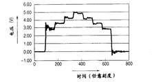
Fig. 8 is the oscillogram of an example by the V14 drive waveforms of electric current equivalent distribution;
Fig. 9 is the structural drawing of the image display device of r*s matrix;
Figure 10 is the oscillogram of the drive waveforms of brightness data in 1/4 o'clock pulse amplitude modulation circuit in prior art of 0~high-high brightness;
Figure 11 is the oscillogram of the drive waveforms of brightness data in 1/4 o'clock pulse amplitude modulation circuit at first embodiment of 0~high-high brightness;
Figure 12 is the equivalent circuit figure of a plurality of light-emitting components of Fig. 1;
Figure 13 is the unit column direction wiring illustraton of model of the equivalent circuit figure of Figure 12;
Figure 14 is the terminal voltage oscillogram of line direction wiring of the model of Figure 13;
Figure 15 is the current waveform figure that flows in the column direction wiring of the model of Figure 13;
Figure 16 is the terminal voltage oscillogram of line direction wiring during by existing drive waveform;
Figure 17 is the current waveform figure that flows during the column direction when passing through to have drive waveform now connects up;
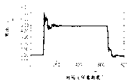
Figure 18 is the oscillogram of an example by the V14 drive waveforms of voltage equivalent distribution;
Figure 19 is the curve of the voltage/luminous intensity characteristic (distribution of voltage equivalent) of light-emitting component;
Figure 20 shows the curve of the V14 driving neutral line of Fig. 8 and Figure 18;
Figure 21 is the oscillogram of a routine Vn drive waveforms;
Figure 22 is the oscillogram of the electric current that flows in modulation waveform that is driven (consistent with the front) by V14 and arbitrary scan wiring Yq;
Figure 23 is the oscillogram of the electric current that flows in modulation waveform that is driven (consistent with the front) by Vn and arbitrary scan wiring Yq;
Figure 24 is the oscillogram of the electric current that flows among the modulation waveform during the combination self-consistentency and the arbitrary scan wiring Yq in Vn drives;
Figure 25 is the oscillogram of the new Vn drive waveforms of an example;
Figure 26 is the oscillogram of the electric current that flows in modulation waveform example that is driven (consistent with the front) by new Vn and arbitrary scan wiring Yq;
Figure 27 is the oscillogram of the electric current that flows among the modulation waveform during the combination self-consistentency and the arbitrary scan wiring Yq in new Vn drives;
Figure 28 shows the component structure of a routine surface conductive type radiated element;
Figure 29 shows the sectional drawing of the component structure of a routine FE type;
Figure 30 shows the sectional drawing of a routine mim type component structure;
Figure 31 is the wiring diagram of the electrical structure of multiple electron beam source;
Figure 32 is the output waveform of existing sweep circuit and pulse amplitude modulation circuit;
Figure 33 is the output waveform of existing sweep circuit and pulse amplitude modulation circuit;
Figure 34 is the structural drawing of multiple electron source;
Figure 35 is the decomposition diagram of the multiple electron source of Figure 34;
Figure 36 is the equivalent circuit figure when selecting all pixels connections that electrode is connected with certain;
Figure 37 is a curve of selecting each several part voltage on the electrode in Figure 36 circuit;
Figure 38 A, 38B, 38C are the drive waveforms figure that is applied in Figure 36 circuit on the distal-most end pixel;
Figure 39 is the oscillogram of signal TV4~TV1 and GV4~GV0 among Fig. 6.
Embodiment
In one embodiment of the invention, the driving energy and the peak value of 1 grade of drive waveforms of increase are peak-peak A
kTimeslot number from N
k-1 becomes N
kIndividual (N wherein
kBe the integer more than 1) time drive waveforms be that this waveform rises to peak A
1Time slot as the 1st time slot, the peak value of the 1st~the k-1 time slot is respectively A
1~A
K-1, the
k~the N
kThe peak value of+k-1 time slot is A
k, N
k+ k~N
kThe peak value of+2 (k-1) time slot is respectively A
K-1~A
1The peak value of the time slot beyond this makes the not driven value of element reality.In addition, relative therewith, drive energy and increase 1 grade drive waveforms by with N
kThe peak value of+2k-1 time slot is not become A by the value that reality drives from element
1, afterwards, N
kThe peak value of+2 (k-1) time slot is from A
1Become A
2..., N
kThe peak value of+k time slot is from A
K-1Become A
k, can form the drive waveforms that 1 grade 1 grade ground increases above-mentioned driving energy.
The establishing method of this waveform also can reverse front and back.
During peak-peak in advance, the above-mentioned peak-peak A when for example comprising k=1
kBecome and compare A
nLittle and peak value is peak-peak A
kTimeslot number from 2 drive waveforms that become 3, above-mentioned driving energy is increased again under 1 grade the situation, replace above-mentioned N
kThe peak value of+2k-1 time slot becomes A from 0
1, the peak value of k+1 time slot is from A
kBecome A
K+1
That is, for to make peak value be A by making driving energy to the drive waveforms of previous stage increase by 1 grade
kTimeslot number from 2 drive waveforms that become 3, the peak value that makes the drive waveforms that drives energy and further increase by 1 grade make above-mentioned drive waveforms is A
k3 time slot central authorities between the time slot peak value from A
kBecome A
K+1Shape.For to make peak value be A by making driving energy to the drive waveforms of previous stage increase by 1 grade
kTimeslot number from 3 drive waveforms that become 4, the peak value that makes the drive waveforms that drives energy and further increase by 1 grade also can make above-mentioned drive waveforms is A
k4 time slots in time slot peak values beyond 2 of two ends from A
kBecome A
K+1Shape.To use the driving method of this drive waveforms row hereinafter referred to as " V14 driving ".
Above-mentioned peak-peak A when comprising k=1
kCompare A
nLittle and above-mentioned N
k+ 2 (k-1) reach the drive waveforms of the maximum timeslot number S (wherein S is the above integer of 2n-1) of regulation, under the situation that further makes 1 grade of above-mentioned driving energy increase, replace above-mentioned N
kThe peak value of+2k-1 time slot is not become A by the peak value that reality drives from element
1, pulse width is (Sk+2k+1)/(k+1) above timeslot number nearest with it, peak-peak is A
K+1, and above-mentioned unit drive waveforms piece number becomes and presents the drive waveforms that the level shape to only many 1 of this drive waveforms rises or descends.In addition, peak value is A
1~A
kIn any and identical time slot have under a plurality of situations, when making above-mentioned driving energy increase by 1 grade afterwards again, peak value diminishes, by near the peak value of the peak value time slot time slot on 1 grade increases 1 grade.
The driving method that uses this drive waveforms row is hereinafter referred to as " Vn driving ".In this Vn drives, the monotone increasing when shifting to an earlier date peak-peak for maintenance, peak value and peak difference are A
n-A
N-1〉=... 〉=A
2-A
1〉=A
1, can be approximately certain, especially, can be A
n-A
N-1=...=A
2-A
1=A
1By peak difference A
n-A
N-1... or A
2-A
1Perhaps peak A
1And the brightness (brightness of corresponding minimum gray shade scale) that the unit drive waveforms piece that determines as the timely crack of the peak difference between the peak value of element drives threshold value width Delta t preferably has respectively with about 1LSB of corresponding brightness data makes the luminous driving energy of above-mentioned light-emitting component.
The additive method of peak-peak is in advance: by comprising the peak-peak A of k=1
kPreferential additional on the lower and peak-peak continuous position by peak difference A
n-A
N-1... or A
2-A
1Perhaps peak A
1And, form above-mentioned drive waveforms as the unit drive waveforms piece that the timely crack of the peak difference between the peak value of element drives threshold value width Delta t determines, be S peak-peak A for maximum timeslot number
kTimeslot number become the drive waveforms of S-2 (k-1), above-mentioned driving energy is further increased under 1 grade the situation, in k+1~S-k time slot arbitrarily time slot preferably with the time slot peak value at the beginning of above-mentioned scope or end from A
kBecome A
K+1The driving method that uses this drive waveforms row is hereinafter referred to as " new Vn drives ".
The following describes embodiments of the invention.
Fig. 1 shows the block scheme of the driving circuit of the multiple electron source that relates to one embodiment of the invention.Among the figure, the 101st, multiple electron source, the 102nd, modulation circuit, the 103rd, sweep circuit, the 104th, timing generating circuit, the 105th, data conversion circuit, the 106th, many power circuits.By this structure, drive multiple electron source 101.Multiple electron source 101 is to constitute electron source (electronic emission element) 1 at the intersection point place of line direction wiring 2 shown in Figure 34 and column direction wiring 3.As electron source, the electronic emission element of above-mentioned SCE type, FE type and mim type is known, in the present embodiment, uses SCE type electronic emission element.
Below, by the block scheme of Fig. 2, describe modulation circuit 102 in detail.Fig. 2 is the block scheme of the inner structure of expression modulation circuit 102.Modulation circuit 102 is made of shift register 107, pwm circuit 108 and output-stage circuit 109.Will be by in the modulating data input shift register 107 of data conversion circuit 105 after the driving data format conversion, transmit column direction with the multiple electron source 101 corresponding modulating data that connects up by shift register 107.Output-stage circuit 109 is to connect many power circuits 106, and output is according to the circuit of drive waveforms of the present invention.Pwm circuit 108 is the circuit that the corresponding pulse width of each output voltage of corresponding modulating data, generation and output-stage circuit 109 exports that connect up of the column direction from shift register 107 input and multiple electron source 101.The timing signal that is used to control shift register 107 and pwm circuit 108 from timing generating circuit 104 inputs.
Further, by the block scheme of Fig. 3, describe pwm circuit 108 in detail.Fig. 3 is the inner structure block scheme of pwm circuit 108.Here, be that example describes with the situation of 4 step voltage output circuits, but be not limited thereto.Pwm circuit 108 begins circuit 111, V2 by latch 110, V1 and begins circuit 112, V3 and begin circuit 113, V4 and begin circuit 114, V1 and finish circuit 115, V2 and finish circuit 116, V3 and finish circuit 117, V4 and finish circuit 118, V1PWM and circuit 119, V2PWM take place circuit 120, V3PWM take place circuit 121 and V4PWM take place circuit 122 takes place constitute.In latch cicuit 110, corresponding Load Signal from timing generating circuit 104 outputs latchs from each modulating data of each shift register 107 outputs.Here, also be used in the timing signal that each pwm signal begins from the Load Signal of timing generating circuit 104 output.
Modulating data after latching in latch cicuit 110 is further imported in the end circuit 115~118 of the beginning circuit 111~114 of V1~V4 and V1~V4.Then, V1 begins the commencing signal of circuit 111 outputs and finishes the end signal input V1PWM circuit 119 that circuit 115 is exported from V1, and 1 corresponding PWM is input to output-stage circuit 109 with output voltage V.Similarly, V2 begins the commencing signal of circuit 112 outputs and finishes the end signal input V2PWM circuit 120 of circuit 116 outputs from V2,2 corresponding PWM are input to output-stage circuit 109 with output voltage V, V3 begins the commencing signal of circuit 113 outputs and finishes the end signal input V3PWM generation circuit 121 of circuit 117 outputs from V3,3 corresponding PWM are input to output-stage circuit 109 with output voltage V, V4 begins the commencing signal of circuit 114 outputs and finishes the end signal input V4PWM generation circuit 122 that circuit 118 is exported from V4, and 4 corresponding PWM are input to output-stage circuit 109 with output voltage V.
Here, for making according to drive waveforms of the present invention, begin the commencing signal that circuit 112 is exported with the time output slower from V2 than the commencing signal that begins circuit 111 outputs from V1, the commencing signal that begins circuit 113 outputs from V3 with the time output slower than the commencing signal that begins circuit 112 output from V2, the commencing signal that begins circuit 114 outputs from V4 with the time output slower than the commencing signal that begins circuit 113 outputs from V3.Further, finish the end signal of circuit 117 outputs from V3 with the time output slower than the end signal that finishes circuit 118 outputs from V4, finish the end signal that circuit 116 is exported with the time output slower from V2, finish the end signal that circuit 115 is exported from V1 with the time output slower than the end signal that finishes circuit 116 outputs from V2 than the end signal that finishes circuit 117 outputs from V3.
Then, describe end circuit 115~118 and the V1~V4PWM circuit 119~122 that V1~V4 begins circuit 111~114 and V1~V4 in detail.Illustrate the 1st circuit example among Fig. 4, the 2nd circuit example among Fig. 5.
Fig. 4 shows to the circuit structure of multiple electron source 101 when the rising edge of the output waveform of a plurality of modulation signal lines is almost consistent simultaneously.Here, only show V1 and begin that circuit 111, V1 finish circuit 115, circuit 119 takes place V1PWM, other beginning circuit, to finish circuit identical with the structure of foregoing circuit with PWM generation circuit.
V1 begins circuit 111 and is made of decoder circuit, count-up counter and comparer.V1 finishes circuit 115 and is made of decoder circuit, count-up counter and comparer, and V1PWM circuit 119 takes place is made of rest-set flip-flop.
In the decoder circuit in V1 begins circuit 111, by being included in the control signal output decoder data in the modulating data.When the output of output valve that V1 begins the decoder circuit in the circuit 111 and count-up counter in V1 begins circuit 111 is consistent, export the V1 commencing signal from the comparers that V1 begins in the circuit 111.Because each gray-level value of modulating data decision signal waveform, so set decoder circuit so that can export and the corresponding data of gray-level value of modulating data.Here, is to use beyond 0 the time as the V1 of the minimum peak in the peak value of non-0 gray-level value of correspondence at the gray-level value of modulating data, therefore be beyond 0 the time at the gray-level value of modulating data, decoder circuit constitutes by compare the output of the commencing signal that output generation regulation output V1 begins with the output valve of count-up counter.In the signal waveform of the gray-level value of corresponding modulating data, whether necessity is also by each gray-level value decision for V2, V3, V4, therefore, in the beginning circuit of V2, V3, V4, decoder circuit is exported the data of comparing with the output of count-up counter accordingly with the gray-level value of modulating data.On the one hand, in the decoder circuit in V1 finishes circuit 111, by being included in the control signal output decoder data in the modulating data.Gray-level value decision by modulating data finishes the time that V1 exports, so the decoder circuit output output corresponding with gray-level value.In the beginning circuit of V2, V3, V4, also be same.When the output of output valve that V1 finishes the decoder circuit in the circuit 111 and count-up counter in V1 finishes circuit 111 is consistent, export the V1 end signal from the comparers that V1 finishes in the circuit 111.
By above commencing signal and end signal are input in the V1PWM generation circuit 119, output is exported corresponding PWM waveform TV1 with V1.In Fig. 4, circuit 119 takes place and is made of rest-set flip-flop in V1PWM.By on the set end S of this rest-set flip-flop, import commencing signal, on reset terminal R the end of input signal, the signal that rises and descend in the input time of end signal is exported from rest-set flip-flop as the PWM waveform TV1 that circuit 119 takes place PWM.In addition,, use rest-set flip-flop circuit 119 to take place here as V1PWM, but J
KOther circuit such as trigger constitute also harmless.
Below, as the 2nd circuit example, Fig. 5 shows the circuit structure when almost consistent simultaneously to the output waveform negative edge of a plurality of modulation signals wiring of multiple electron source 101.V1 begins circuit 111 and is made of decoder circuit, down counter and comparer.V1 finishes circuit 115 and is made of decoder circuit, down counter and comparer, and V1PWM circuit 119 takes place is made of rest-set flip-flop.Here, only show V1 and begin that circuit 111, V1 finish circuit 115, circuit 119 takes place V1PWM, other beginning circuit, to finish circuit identical with the structure of foregoing circuit with PWM generation circuit.In the decoder circuit in V1 begins circuit 111, by being included in the control signal output decoder data in the modulating data.When the output of output valve that V1 begins the decoder circuit in the circuit 111 and down counter in V1 begins circuit 111 is consistent, export the V1 commencing signal from the comparers that V1 begins in the circuit 111.In the decoder circuit in V1 begins circuit 111, by being included in the control signal output decoder data in the modulating data.When the output of output valve that V1 finishes the decoder circuit in the circuit 111 and down counter in V1 finishes circuit 111 is consistent, finishes the comparer of circuit from V1 and export the V1 end signal.By above commencing signal and end signal are input in the PWM generation circuit 119, output is exported corresponding PWM waveform TV1 with V1.
Each column direction wiring of said PWM circuit 108 and output-stage circuit 109 corresponding multiple electron sources 101 can be used Fig. 4 or circuit shown in Figure 5, but as the 3rd embodiment, in column direction wiring,, the rising edge one negative edge unanimity of making peace is carried out alternately by mutual design drawing 4 circuit and Fig. 5 circuit.
Fig. 6 shows with the circuit of each column direction wiring 1 example as Fig. 2 and output-stage circuit 109 shown in Figure 3.In the circuit of Fig. 6, current potential V1~V4,0<V1<V2<V3<V4 is respectively with the corresponding output of PWM output waveform TV1~TV4.Q1~Q4 is transistor or the pair transistor that respectively current potential V1~V4 is outputed to lead-out terminal Out when conducting.PWM output waveform TV1~TV4 is, even wherein more than 2 be the H level, transistor Q1~Q4 more than 2 is not conducting simultaneously also, and, only will output to lead-out terminal Out, be applied to control utmost point GV1~GV4 of each transistor Q1~Q4 by logical circuit with maximum current potential among the corresponding current potential V1~V4 of PWM output waveform TV1~TV4 of H level.Figure 39 shows the waveform of a routine TV1~TV4 and GV1~GV4.
Voltage/luminous intensity characteristic that Fig. 7 shows LED and electronic emission element has the voltage/luminous intensity characteristic of the light-emitting component of non-linear threshold characteristic.Transverse axis represents to apply voltage, and the longitudinal axis is represented luminous intensity.Each drive level current potential by setting V1, V2, V3, V4 is so that luminous strength ratio becomes 1: 2: 3: 4, and aAb, c, each regional luminous quantity of d are of equal value in the time changing curve of luminous quantity.Promptly, by the most suitably setting each drive level current potential of V1, V2, V3, V4, can make by unit pulse width Delta t that represents in the drive waveforms time changing curve and unit peak value is that voltage difference is that the luminous quantity of the unit drive waveforms piece of the A, the B that constitute of V4-V3, V3-V2, V2-V1, V1-V0, C, D equates.Here, decision current potential V1~V4 is so that the luminous quantity of constituent parts drive waveforms piece A~D is approximately consistent with the 1LSB (1 gray shade scale) of brightness data.
In addition, in element, provide the selection current potential as basic current potential by scanning signal lines.Here, select current potential to be-9.9V.When considering to be applied to voltage on this element and ignoring influencing of voltage drop, the level of drive signal is respectively V1-(9.9) [V], V2-(9.9) [V], V3-(9.9) [V], V4-(9.9) [V] when V1, V2, V3, V4.In addition, select V0 so that V1-(9.9) [V] changes to below the driving voltage threshold value of element.Here, with V0 as earthing potential.Its value is identical with the drive threshold of element.The driving voltage threshold value that is element is 9.9[V].
Fig. 8 shows the V14 drive waveforms as an example of the drive waveforms shape that is used to represent gray shade scale.In Fig. 8, the signal of each gray shade scale is made up of the unit drive waveforms piece of the number corresponding with its gray shade scale number.1 gray shade scale is made up of 1 unit drive waveforms piece, and 2 gray shade scales are made up of 2 unit drive waveforms pieces, thereby the N gray shade scale is made up of N unit drive waveforms piece.Among the figure, the unit drive waveforms piece of the blank spot of N gray shade scale is represented the difference with the N-1 gray shade scale.In the drive waveforms of N-1 gray shade scale, by the unit drive block being appended to the drive waveforms that forms the N gray shade scale on the continuous position of drive waveforms.By forming such drive waveforms, during voltage/luminous intensity characteristic variations, also can guarantee the dull property that increases when between light-emitting component, having deviation.
In the present embodiment, in order to represent the view data of the long R=10 of data bit, unit pulse to the time slot width Δ t that uses the P=9 position in 0~259 scope carries out pulse width control, is that 1~4 level is to carry out peak value (amplitude) control with the Q=2 position that comprises 1 of residue in the scope of peak value V1~V4 at the peak level.That is, for representing 10 bit image data, above-mentioned R, P, each data of Q keep the relation of R<P+Q.
During R=P+Q, for example, in peak value control, use preceding 2, when carrying out pulse width control, can not show 10 view data altogether during for the level shape at the negative edge of drive waveforms to remaining 8.Be that the gray shade scale number descends.But, in the present embodiment,, thus, can show 10 view data altogether because R<P+Q carries out pulse width with 9 and controls.
As shown in Figure 8, when the drive waveforms when the highest drive level of N gray shade scale is k rises, will be from 1 level (current potential V1) to k level (current potential V
k) drive waveforms export whole level by the order from the low level to the high level, and remain on more than the unit pulse width Delta t by output with each level, can reduce the electric current that flows when drive waveforms rises.
Similarly, when drive waveforms descends, will be from k level (current potential V
k) export whole level to the drive waveforms of 1 level (current potential V1) by order from high to low, and remain on more than the unit pulse width Delta t by the output with each level, the electric current that flows when drive waveforms descends can be reduced.
The equivalent circuit of multiple optical element has been shown among Figure 12.In reality drives, apply the selection current potential for the line direction wiring of selecting 2, apply the driving current potential to column direction wiring 3, for ease of understanding simplified model, use the single direction cloth line model that ranks shown in Figure 13 to carry out emulation.By dead resistance is that 10 Ω, stray inductance are that 300nH, stray capacitance are that 10pF, modulation circuit are 4 kinds power supply and MOS transistor formation.
In the circuit of Figure 13, carry out emulation during the drive waveforms of 9 gray shade scales under V0=0V, V1=3V, V2=3.7V, V3=4.4V, V4=5.0V condition among driving Fig. 8.The terminal voltage waveform of line direction wiring is shown in Figure 14, and the current waveform that flows into the column direction wiring is shown in Figure 15.
Be situation about relatively driving under V0=0V, V1=V2=V3=V4=5.0V condition, the terminal voltage waveform of line direction wiring in the time of will be with existing drive waveform is shown in Figure 16, and the current waveform that flows into the column direction wiring is shown in Figure 17.
In the occasion that drives with drive waveforms of the present invention (Fig. 8), the convergence that flows into the electric current of column direction wiring is 1/2nd a degree with existing drive waveform.Its result crosses emission voltage with existing drive waveform the time and produces the 2V degree and compare, and when driving with the drive waveforms of present embodiment, crossing emission voltage is the 0.8V degree.
That is,,, can provide and can realize high gray shade scale, guarantee the gray shade scale monotone increasing with the driving circuit of cheapness according to present embodiment, light-emitting component uniformly light-emitting, shot noise reduces, drive waveforms is stable drive waveforms and driving method.
The 2nd embodiment
Figure 18 shows other examples of V14 drive waveforms.The drive waveforms of Fig. 8 illustrates each drive level current potential of know clearly setting V1, V2, V3, V4 so that luminous strength ratio becomes 1: 2: 3: 4 o'clock example.In LED and electronic emission element, luminous intensity and drive current are approximately proportional, therefore, below are referred to as electric current etc. and cut apart mode.On the one hand, Figure 18 determines that V1, V2, V3, V4 are so that their ratio becomes 1: 2: 3: 4, be potential difference (PD) V4-V3, V3-V2, V2-V1, V1-V0 (here, the reference potential V0 of drive waveforms is identical with the drive threshold of element) become definite value, therefore, below be referred to as voltage etc. and cut apart mode.Figure 19 shows voltage etc. and cuts apart voltage/current (luminous intensity) in the mode.
In Figure 18, the unit drive waveforms piece of the blank spot of N gray shade scale is represented the difference with the N-1 gray shade scale.In the drive waveforms of N-1 gray shade scale, form the drive waveforms of N gray shade scale by additional 1 unit drive block on the continuous position of drive waveforms.The relation of luminous quantity a~d of the drive block A~D of unit of the Figure 19 that uses in Figure 18 is a<b<c<d.Therefore, in the waveform of the certain Fig. 8 of the luminous quantity of the drive block A~D of unit, difference for 3 gray shade scales and 4 gray shade scales is the situation of the drive block B of unit, and in the waveform of Figure 18, the drive block A of unit is that 3 gray shade scales of low gray shade scale and the variation between 4 gray shade scales diminish.
Figure 20 shows the linearity in the V14 driving.When changing voltage, luminous intensity characteristic, also can guarantee dull incremental when between light-emitting component, having deviation by forming this drive waveforms.
As shown in figure 18, when the drive waveforms when the highest drive level of N gray shade scale is k rises, will be from 1 level (current potential V1) to k level (current potential V
k) drive waveforms export whole level by the order from the low level to the high level, and remain on more than the unit pulse width Delta t by output with each level, can reduce the electric current that flows when drive waveforms rises.
Similarly, when drive waveforms descends, will be from k level (current potential V
k) export whole level to the drive waveforms of 1 level (current potential V1) by order from high to low, and remain on more than the unit pulse width Delta t by the output with each level, the electric current that flows when drive waveforms descends can be reduced.
The 3rd embodiment
Figure 21 shows a routine Vn drive waveforms.When this waveform was made of the R position at brightness data, brightness data was about 0<N≤((2
R) k/n-1) time, be the drive waveform of k (k is less than the integer of n more than 1) with the peak value of the drive waveforms of data N.In the drive waveforms of Fig. 8, peak value k is 3 when following, unit drive block number (timeslot number) of the peak value k of the drive waveforms by making the n-1 gray shade scale on the drive waveforms that the unit drive block is appended to the n-2 gray shade scale becomes at 3 o'clock, in the drive waveforms of n gray shade scale below, drive waveforms to the unit drive block that added peak value k+1, when in the drive waveforms of Figure 21, increasing gray shade scale, (1 level: the maximum number S (being 259 in the present embodiment) that unit drive block number minimum peak) reaches regulation does not carry out shifting to an earlier date of peak value (level) to peak value 1 before, when reaching maximum number S and then increasing by 1 grade, the unit drive block number of 1 level becomes (Sk+2k+1)/(k+1) above number nearest with it, and, carry out repeatedly, in advance so that the piece number of the level more than 1 lacks 2 or 3 than the piece number of following level respectively.
For example, during S=259, in the 259th gray shade scale, the unit drive block number of 1 level and 259 become complete together, in the 260th gray shade scale of following, becoming 1 level and be 131 and 2 level is 129, same, in the 516th gray shade scale, 1 level is that 259 and 2 level are 257, and the unit drive block number of 1 level becomes complete, in the 517th gray shade scale of following, 1 level is 175,2 level are 172,3 level are 170, and in the 771st gray shade scale, 1 level is 259,2 level are 257,3 level are 255, the unit drive block number of 1 level becomes complete, in the 772nd gray shade scale of following, 1 level is 196,2 level are 194,3 level are 192,4 level are 190, and peak-peak shifts to an earlier date singly.
In the drive waveforms of Figure 21, n=4, k=1 are that brightness data is 1/4 o'clock of 0~high-high brightness, to existing pulse amplitude modulation waveform, by the actual effect that makes the pulse amplitude modulation amplitude of wave form partly be 1/4, pulse width is 4 to be carried out driving, the electric current that flows in light-emitting component 1 each element becomes i/4, and the electric current that flows in the line direction wiring of selecting also becomes r*i/4.Therefore, falling quantity of voltages also can be reduced to 1/4, the voltage reduction that is applied on the light-emitting component can be reduced to 1/4.Similarly, n=4, k=2 are that brightness data is 1/2 o'clock of 0~high-high brightness, and falling quantity of voltages can reduce to 1/2, and n=4, k=3 are brightness data when being 0~high-high brightness 3/4, and falling quantity of voltages can reduce to 3/4.
Fig. 9 shows the image display device of r * s matrix.It is the drive waveforms of brightness data at the pulse amplitude modulation circuit of 1/4 o'clock prior art of 0~high-high brightness that Figure 10 shows n=4, k=1.As can be seen, among the line direction wiring Yq that the electric current that flows in each element of light-emitting component 1 is selected during for i, produce voltage drop by flowing through the r*I electric current, the voltage that imposes on light-emitting component reduces.
It is the drive waveforms of brightness data at the pulse amplitude modulation circuit of 1/4 o'clock present embodiment of 0~high-high brightness that n=4, k=1 have been shown among Figure 11.The actual effect part that the amplitude of the pulse amplitude modulation waveform of knowing clearly is shown (is removed the part that is included in the part in the driving voltage threshold value from amplitude; In the present embodiment, as the V0 conduct of the reference potential of modulation waveform and the identical value of drive threshold of element, deduct the amplitude of the part=modulation waveform of the part that is included in the element drives voltage threshold from the amplitude of modulation waveform) be 1/4, pulse width is 4 times of situations about driving.The electric current that flows in light-emitting component 1 each element is I/4, and the electric current that flows in the line direction wiring of selecting also is r*I/4.Therefore falling quantity of voltages also can be reduced to 1/4, the voltage reduction that is applied on the light-emitting component can be reduced to 1/4.
Similarly, n=4, k=2 are that brightness data is 1/2 o'clock of 0~high-high brightness, and falling quantity of voltages can reduce to 1/2, and n=4, k=3 are brightness data when being 0~high-high brightness 3/4, and falling quantity of voltages can reduce to 3/4.
In Figure 22, the V14 that shows the 1st or the 2nd embodiment drives the example of modulation waveform in (consistent with the front) and the electric current that flows in any scanning lines Yq.In Figure 23, illustrate as the Vn of present embodiment and drive the example of modulation waveform of (consistent) and the electric current that in scanning lines Yq arbitrarily, flows with the front.Obviously, the Vn type of drive of present embodiment has reduced the current peak that flows significantly by making the electric current equalization in scanning lines.
In Figure 24, show the electric current that flows among scanning lines (line direction wiring) Yq when also using self-consistentency in the Vn driving.Electric current is by further equalization.Here, consistent with the front, the rising edge part that is controlled to drive waveforms is at 1 first half during selecting, in time, is preferably in the regulation time slot of first half of pulse width control and produces initial unit drive block.Consistent with the back, the negative edge part that is controlled to drive waveforms is at 1 latter half during selecting, in time, is preferably in the regulation time slot of latter half of pulse width control and produces last unit drive block.In addition, when fixing the time slot of these regulations, can set 1 initial time slot group during selecting is first half regulation time slot, sets final time slot and stipulates time slot as latter half, but also can set inboard time slot.In the wiring of each column direction,, can set time slot of each regulation in first half or the latter half by its column direction wiring or the wiring of other column directions corresponding gray shade scale or modulation waveform with the light-emitting component that drives.Perhaps, corresponding with the gray shade scale or the modulation waveform of a plurality of light-emitting components of selecting simultaneously, identical time slot can be set at partly preceding or each regulation time slot of latter half to the full column direction wiring that drives them.
The 4th embodiment
In Figure 25, show new Vn drive waveforms.This drive waveforms is when increasing gray shade scale, reaching the unit drive block that regulation maximum number S (being 259 in the present embodiment) at first disposes peak value 1 (1 level) before, then, the unit drive block of configuration 2 level (current potential V2) before reaching the S-1 time slot since the 2nd time slot, ..., since k time slot configuration k level (current potential V before arriving the S+1-k time slot
k) the unit drive block, become the good drive waveforms of configuration sequence.
Figure 26 shows new Vn and drive the example of modulation waveform in (consistent with the front) and the electric current that flows in any sweep trace Yq.Electric current averages out.Further, by driving with new Vn and can making as shown in figure 27 electric current mobile in scanning lines Yq almost even in during 1H with self-consistentency.
Here, in matrix panel, calculate the effect that reduces of electric current mobile in the information wiring with 1920 * 3 information wirings and 1024 scanning lines.The electric current that flows in element is 0.8mA to the maximum, as shown in Figure 7, set modulation waveform so that wait when cutting apart drive current, the maximal value that the electric current of each element changed when existing dull PWM and V14 drove is 0.8mA, the maximal value Δ Iy that the electric current of each scanning lines changes is Δ Iy=0.8mA * 1920 * 3=4.608A, by and become 1/2 with self-consistentency, so Δ Iy=2.304A, the situation that new Vn drives is to remove the rising edge of waveform, the electric current variation is 0.8mA/4=0.2mA in the part of negative edge part, therefore, Δ Iy=0.2mA * 1920 * 3=1.152A, further, and consistent with 1 element the place ahead when driving with self-consistentency, the rear is consistent because become 1/2 repeatedly, becomes Δ Iy=576mA.
The variation of embodiment
Drive and during the new Vn of Figure 25 drives at the Vn of Figure 21, modulation waveform can set that drive current as shown in Figure 7 etc. is cut apart for, the actual effect of driving potential amplitude as shown in figure 19 partly etc. is cut apart.For the coupling that prevents to take place when the waveform rise and fall and the potential difference (PD) of crossing emission and basic current potential become the current potential (V0) of the driving voltage threshold value of element, and make the voltage between V1, V2, V3 and V4 equate it is effective.The relation that applies voltage and luminous quantity when Figure 19 shows etc. and to cut apart the actual effect part that drives potential amplitude.Obviously, the luminous quantity of the unit drive waveforms piece of the A, the B that constitute of unit pulse width of representing in the time changing curve by drive waveforms and unit peak value, C, D is unequal.
Figure 20 shows V14 and carries out electric current etc. in driving when cutting apart and brightness and the data relationship when cutting apart such as voltage.In low brightness area, the linear damage, but guaranteed monotone increasing, can handle by the data revisal.
In the γ revisal, set coupling and take place by cutting apart with the voltage of the V1~V4 of Min. ground output etc., brightness data becomes the curve also darker than the contrary γ characteristic of normally used 2.2 powers (the brightness resolution uprises in low brightness area) to the relation of brightness.Its result, when contrary gamma transformation, can improve from low-light level to the brightness resolution of brightness.
In the above-described embodiments, enumerate the example of 1024 gray shade scales of the gray shade scale number from 0 to 1023 of the peak value control of carrying out 4 level, but in the present invention, do not control the qualification of peak value, gray shade scale number.
In the present invention, in the driving circuit of cheapness, can provide and can realize high gray shade scale, guarantee the gray shade scale monotone increasing, light-emitting component uniformly light-emitting, shot noise reduces, drive waveforms is stable drive waveforms, driving method.In the driving circuit of cheapness, provide the luminous element control method that can reduce the Luminance Distribution deviation.
Claims (12)
1. driving circuit that is used for drive unit, it is characterized in that, this driving circuit comprises output, and at least one has the circuit of the drive signal of drive waveforms, pulse width to this drive waveforms is that unit controls with time slot width Δ t, and the peak value in each time slot of this drive waveforms is defined as A
1-A
nIn one, wherein n is integer and n 〉=2, A
1<A
2<...<A
n, A
1-A
nCorresponding to the non-zero gray-scale value, for having the regulation of rising to peak A
kThe whole described drive waveforms of rising part, this rising part at least by a time slot in order through the peak A of associating
1To peak A
K-1Corresponding to less than A
kThe peak value of non-zero gray-scale value, until rising to described regulation peak A
k, wherein k is integer and 2≤k≤n.
2. driving circuit that is used for drive unit, it is characterized in that, this driving circuit comprises output, and at least one has the circuit of the drive signal of drive waveforms, pulse width to this drive waveforms is that unit controls with time slot width Δ t, and the peak value in each time slot of this drive waveforms is defined as A
1-A
nIn one, wherein n is integer and n 〉=2, A
1<A
2<...<A
n, A
1-A
nCorresponding to the non-zero gray-scale value, in this circuit, for having from the regulation peak A
kThe whole described drive waveforms of the sloping portion of beginning, this sloping portion is from described regulation peak A
kBegin to descend, at least by a time slot in order through the peak A of associating
K-1To peak A
1Corresponding to less than A
kThe peak value of non-zero gray-scale value, wherein k is integer and 2≤k≤n.
3. display device comprises:
A plurality of light-emitting components, many scanning signal lines and many root informations signal routing; And
The described driving circuit of claim 1, wherein this driving circuit provides the drive signal with described drive waveforms to described many root informations signal routing.
4. display device according to claim 3 is characterized in that,
Begin to rise from described drive waveforms until reaching described peak A
kTime, can be configured to approximate or greater than time by the 0%-90% time constant that driving force determined of the load of described information signal wiring and described driving circuit.
5. display device according to claim 3, it is characterized in that, further comprise the sweep circuit that is connected to described scanning signal lines, thereby the described drive signal Be Controlled that wherein is applied to the first selected information signal wiring in the wiring of described information signal selects the preceding half section during the selection of described scanning signal lines to begin to rise at described sweep circuit, thereby the later half period of described drive signal Be Controlled during described selection that is applied to the second selected information signal wiring in the described information signal wiring begins to descend.
6. display device according to claim 3 is characterized in that,
The time shaft that is applied to the described drive waveforms of the described drive signal of the first selected information signal wiring in the wiring of described information signal be configured to be applied to described information signal wiring in the time shaft of described drive waveforms of the described drive signal that connects up of the second selected information signal opposite.
7. display device according to claim 3 is characterized in that,
Described driving circuit further comprises a modulation circuit that receives R position brightness data as pictorial data, at timeslot number 2
POr be that unit controls described pulse width with the time slot in the littler scope, and carry out n=2
QThe peak value control of level, described R, P, Q satisfy the relation of R<P+Q, and wherein P and Q are figure places.
8. display device comprises:
A plurality of light-emitting components, many scanning signal lines and many root informations signal routing; And
The described driving circuit of claim 2, wherein this driving circuit provides the drive signal with described drive waveforms to described many root informations signal routing.
9. display device according to claim 8, it is characterized in that, further comprise the sweep circuit that is connected to described scanning signal lines, thereby the described drive signal Be Controlled that wherein is applied to the first selected information signal wiring in the wiring of described information signal selects the preceding half section during the selection of described scanning signal lines to begin to rise at described sweep circuit, thereby the later half period of described drive signal Be Controlled during described selection that is applied to the second selected information signal wiring in the described information signal wiring begins to descend.
10. display device according to claim 8 is characterized in that,
The time shaft that is applied to the described drive waveforms of the described drive signal of the first selected information signal wiring in the wiring of described information signal be configured to be applied to described information signal wiring in the time shaft of described drive waveforms of the described drive signal that connects up of the second selected information signal opposite.
11. display device according to claim 8 is characterized in that,
Described driving circuit further comprises a modulation circuit that receives R position brightness data as pictorial data, at timeslot number 2
POr be that unit controls described pulse width with the time slot in the littler scope, and carry out n=2
QThe peak value control of level, described R, P, Q satisfy the relation of R<P+Q, and wherein P and Q are figure places.
12. display device according to claim 8 is characterized in that, each light-emitting component comprises a surface conduction type luminescent device.
Applications Claiming Priority (8)
| Application Number | Priority Date | Filing Date | Title |
|---|---|---|---|
| JP2001181841 | 2001-06-15 | ||
| JP181841/2001 | 2001-06-15 | ||
| JP248978/2001 | 2001-08-20 | ||
| JP2001248978 | 2001-08-20 | ||
| JP2001296397 | 2001-09-27 | ||
| JP296397/2001 | 2001-09-27 | ||
| JP2002167096A JP3681121B2 (en) | 2001-06-15 | 2002-06-07 | Driving circuit and display device |
| JP167096/2002 | 2002-06-07 |
Related Parent Applications (1)
| Application Number | Title | Priority Date | Filing Date |
|---|---|---|---|
| CNB021429154A Division CN100483494C (en) | 2001-06-15 | 2002-06-14 | Drive circuit, display device and driving method |
Publications (2)
| Publication Number | Publication Date |
|---|---|
| CN1652173A CN1652173A (en) | 2005-08-10 |
| CN100394466C true CN100394466C (en) | 2008-06-11 |
Family
ID=27482344
Family Applications (2)
| Application Number | Title | Priority Date | Filing Date |
|---|---|---|---|
| CNB021429154A Expired - Fee Related CN100483494C (en) | 2001-06-15 | 2002-06-14 | Drive circuit, display device and driving method |
| CNB2005100528263A Expired - Fee Related CN100394466C (en) | 2001-06-15 | 2002-06-14 | Drive circuit, display device and driving method |
Family Applications Before (1)
| Application Number | Title | Priority Date | Filing Date |
|---|---|---|---|
| CNB021429154A Expired - Fee Related CN100483494C (en) | 2001-06-15 | 2002-06-14 | Drive circuit, display device and driving method |
Country Status (5)
| Country | Link |
|---|---|
| US (2) | US6995516B2 (en) |
| EP (1) | EP1267319A2 (en) |
| JP (1) | JP3681121B2 (en) |
| KR (3) | KR100557183B1 (en) |
| CN (2) | CN100483494C (en) |
Families Citing this family (42)
| Publication number | Priority date | Publication date | Assignee | Title |
|---|---|---|---|---|
| TWI280547B (en) * | 2000-02-03 | 2007-05-01 | Samsung Electronics Co Ltd | Liquid crystal display and driving method thereof |
| JP3647426B2 (en) * | 2001-07-31 | 2005-05-11 | キヤノン株式会社 | Scanning circuit and image display device |
| JP3715967B2 (en) * | 2002-06-26 | 2005-11-16 | キヤノン株式会社 | DRIVE DEVICE, DRIVE CIRCUIT, AND IMAGE DISPLAY DEVICE |
| JP4320413B2 (en) * | 2002-09-11 | 2009-08-26 | 日本電気株式会社 | Semiconductor integrated circuit and layout design apparatus |
| JP3830888B2 (en) * | 2002-12-02 | 2006-10-11 | オプトレックス株式会社 | Driving method of organic EL display device |
| JP4136670B2 (en) * | 2003-01-09 | 2008-08-20 | キヤノン株式会社 | Matrix panel drive control apparatus and drive control method |
| JP4332358B2 (en) * | 2003-01-30 | 2009-09-16 | キヤノン株式会社 | Driving circuit |
| JP3880540B2 (en) | 2003-05-16 | 2007-02-14 | キヤノン株式会社 | Display panel drive control device |
| JP4012118B2 (en) | 2003-05-19 | 2007-11-21 | キヤノン株式会社 | Image display device |
| JP4035490B2 (en) | 2003-08-15 | 2008-01-23 | キヤノン株式会社 | Image display device manufacturing method and image display device |
| KR100599649B1 (en) * | 2003-11-24 | 2006-07-12 | 삼성에스디아이 주식회사 | Driving apparatus of plasma display panel |
| JP2005257791A (en) * | 2004-03-09 | 2005-09-22 | Canon Inc | Image display apparatus and driving method for same |
| JP2005292804A (en) * | 2004-03-10 | 2005-10-20 | Canon Inc | Control device and image display device |
| JP4086852B2 (en) | 2004-03-16 | 2008-05-14 | キヤノン株式会社 | Image display device |
| KR101022657B1 (en) * | 2004-05-31 | 2011-03-22 | 삼성에스디아이 주식회사 | Driving method of electron emission device |
| US7227317B2 (en) * | 2004-06-10 | 2007-06-05 | Atmel Corporation | Method and system for enhanced dimming resolution in a light ballast through use of multiple control frequencies |
| JP2006047997A (en) | 2004-06-30 | 2006-02-16 | Canon Inc | Modulation circuit, driving circuit, and output method |
| CN100428294C (en) * | 2004-06-30 | 2008-10-22 | 佳能株式会社 | Modulation circuit, driving circuit and output method |
| CN100390840C (en) * | 2004-06-30 | 2008-05-28 | 佳能株式会社 | Display apparatus and method for controlling the same |
| JP4174494B2 (en) | 2004-06-30 | 2008-10-29 | キヤノン株式会社 | Drive device, image display device, and television device |
| JP4560445B2 (en) | 2004-06-30 | 2010-10-13 | キヤノン株式会社 | Display device and driving method |
| JP4908784B2 (en) * | 2004-06-30 | 2012-04-04 | キヤノン株式会社 | Display element drive circuit, image display device, and television device |
| US20060050031A1 (en) * | 2004-09-06 | 2006-03-09 | Sanyo Electric Co., Ltd. | Display-device driving circuit suitable for inorganic electroluminescence (EL) display device |
| JP2006186277A (en) * | 2004-12-28 | 2006-07-13 | Sanyo Electric Co Ltd | Light-emitting element driving device |
| KR100676190B1 (en) * | 2005-05-17 | 2007-01-30 | 엘지전자 주식회사 | Organic electroluminescent device |
| JP4494298B2 (en) * | 2005-06-24 | 2010-06-30 | シャープ株式会社 | Driving circuit |
| KR100732809B1 (en) * | 2005-11-03 | 2007-06-27 | 삼성에스디아이 주식회사 | Data Driver and Organic Light Emitting Display Using the same |
| US8373355B2 (en) * | 2006-11-09 | 2013-02-12 | Apple Inc. | Brightness control of a status indicator light |
| JP4861937B2 (en) * | 2007-09-11 | 2012-01-25 | オムロン株式会社 | Transmission device, reception device, transmission / reception device, transmission control method, reception control method, optical transmission module, electronic device |
| JP2009211052A (en) * | 2008-02-06 | 2009-09-17 | Canon Inc | Drive circuit of display panel and display apparatus |
| JP2009251046A (en) | 2008-04-01 | 2009-10-29 | Canon Inc | Image display apparatus and control method of the same |
| WO2010014359A2 (en) * | 2008-08-01 | 2010-02-04 | Sipix Imaging, Inc. | Gamma adjustment with error diffusion for electrophoretic displays |
| JP2010145739A (en) * | 2008-12-18 | 2010-07-01 | Sanyo Electric Co Ltd | Light-emitting element driving circuit |
| JP2011018012A (en) * | 2009-06-08 | 2011-01-27 | Canon Inc | Control method for image display apparatus |
| JP2011002651A (en) * | 2009-06-18 | 2011-01-06 | Canon Inc | Image display device and control method of image display device |
| US8138687B2 (en) * | 2009-06-30 | 2012-03-20 | Apple Inc. | Multicolor lighting system |
| WO2011026217A1 (en) | 2009-09-02 | 2011-03-10 | Scobil Industries Corp. | Method and apparatus for driving an electroluminescent display |
| US8400626B2 (en) | 2010-06-10 | 2013-03-19 | Apple Inc. | Ambient light sensor |
| JP2013083826A (en) * | 2011-10-11 | 2013-05-09 | Canon Inc | Liquid crystal display device, control method of liquid crystal display device |
| CN103247251B (en) * | 2012-02-03 | 2015-06-03 | 深圳市明微电子股份有限公司 | Integral modulation control method and system for LED driver chip |
| US10455653B1 (en) * | 2018-08-09 | 2019-10-22 | Innolux Corporation | LED driving circuits |
| US11835382B2 (en) | 2021-03-02 | 2023-12-05 | Apple Inc. | Handheld electronic device |
Citations (4)
| Publication number | Priority date | Publication date | Assignee | Title |
|---|---|---|---|---|
| JP2000148074A (en) * | 1998-11-06 | 2000-05-26 | Victor Co Of Japan Ltd | Matrix type display device |
| JP2000250471A (en) * | 1999-02-25 | 2000-09-14 | Canon Inc | Driving device and method for multiple electron source and image forming device |
| JP2000276095A (en) * | 1999-03-25 | 2000-10-06 | Victor Co Of Japan Ltd | Matrix type display device |
| JP2000310971A (en) * | 1999-02-26 | 2000-11-07 | Canon Inc | Picture display device and display control method |
Family Cites Families (45)
| Publication number | Priority date | Publication date | Assignee | Title |
|---|---|---|---|---|
| US4904895A (en) | 1987-05-06 | 1990-02-27 | Canon Kabushiki Kaisha | Electron emission device |
| US5066883A (en) | 1987-07-15 | 1991-11-19 | Canon Kabushiki Kaisha | Electron-emitting device with electron-emitting region insulated from electrodes |
| JPS6431332A (en) | 1987-07-28 | 1989-02-01 | Canon Kk | Electron beam generating apparatus and its driving method |
| JPH0518585Y2 (en) | 1987-08-13 | 1993-05-18 | ||
| JPH02257551A (en) | 1989-03-30 | 1990-10-18 | Canon Inc | Image forming device |
| JP3044382B2 (en) | 1989-03-30 | 2000-05-22 | キヤノン株式会社 | Electron source and image display device using the same |
| US5682085A (en) | 1990-05-23 | 1997-10-28 | Canon Kabushiki Kaisha | Multi-electron beam source and image display device using the same |
| JP2967288B2 (en) | 1990-05-23 | 1999-10-25 | キヤノン株式会社 | Multi electron beam source and image display device using the same |
| JP3165701B2 (en) * | 1991-03-06 | 2001-05-14 | キヤノン株式会社 | Vibration wave motor |
| JP2901032B2 (en) | 1992-01-31 | 1999-06-02 | 京セラ株式会社 | LED print head |
| JP3167072B2 (en) | 1992-12-29 | 2001-05-14 | キヤノン株式会社 | Image forming device |
| US5455597A (en) | 1992-12-29 | 1995-10-03 | Canon Kabushiki Kaisha | Image-forming apparatus, and designation of electron beam diameter at image-forming member in image-forming apparatus |
| CA2112431C (en) | 1992-12-29 | 2000-05-09 | Masato Yamanobe | Electron source, and image-forming apparatus and method of driving the same |
| CA2112733C (en) | 1993-01-07 | 1999-03-30 | Naoto Nakamura | Electron beam-generating apparatus, image-forming apparatus, and driving methods thereof |
| US6157137A (en) | 1993-01-28 | 2000-12-05 | Canon Kabushiki Kaisha | Multi-electron beam source with driving circuit for preventing voltage spikes |
| JP3235893B2 (en) | 1993-01-28 | 2001-12-04 | 京セラ株式会社 | Drive circuit for liquid crystal display |
| JP3205167B2 (en) | 1993-04-05 | 2001-09-04 | キヤノン株式会社 | Method of manufacturing electron source and method of manufacturing image forming apparatus |
| JPH075836A (en) | 1993-04-05 | 1995-01-10 | Canon Inc | Device and method for forming image |
| FR2708129B1 (en) | 1993-07-22 | 1995-09-01 | Commissariat Energie Atomique | Method and device for controlling a fluorescent microtip screen. |
| JPH07177446A (en) | 1993-12-17 | 1995-07-14 | Matsushita Electric Ind Co Ltd | Image display device |
| CA2138363C (en) * | 1993-12-22 | 1999-06-22 | Yasuyuki Todokoro | Electron beam generating apparatus, image display apparatus, and method of driving the apparatuses |
| US5477110A (en) | 1994-06-30 | 1995-12-19 | Motorola | Method of controlling a field emission device |
| JPH09101759A (en) * | 1995-10-04 | 1997-04-15 | Pioneer Electron Corp | Method and device for driving light emitting element |
| JP3278375B2 (en) | 1996-03-28 | 2002-04-30 | キヤノン株式会社 | Electron beam generator, image display device including the same, and method of driving them |
| JPH09281928A (en) | 1996-04-16 | 1997-10-31 | Pioneer Electron Corp | Display device |
| JPH1039825A (en) | 1996-07-23 | 1998-02-13 | Canon Inc | Electron generation device, picture display device, and their driving circuit and driving method |
| JP4059537B2 (en) | 1996-10-04 | 2008-03-12 | 三菱電機株式会社 | Organic thin film EL display device and driving method thereof |
| JP3027126B2 (en) | 1996-11-26 | 2000-03-27 | 松下電器産業株式会社 | Liquid crystal display |
| CN2300165Y (en) * | 1996-11-27 | 1998-12-09 | 矽诚科技股份有限公司 | Electroluminescent plate driving device |
| JPH1115430A (en) | 1997-06-19 | 1999-01-22 | Yamaha Corp | Electric field emission display device |
| JP3049061B1 (en) | 1999-02-26 | 2000-06-05 | キヤノン株式会社 | Image display device and image display method |
| JP3644240B2 (en) * | 1998-03-24 | 2005-04-27 | セイコーエプソン株式会社 | Digital driver circuit for electro-optical device and electro-optical device including the same |
| JP3554185B2 (en) | 1998-04-03 | 2004-08-18 | キヤノン株式会社 | Electron source driving device and image forming apparatus using the same |
| US6489940B1 (en) | 1998-07-31 | 2002-12-03 | Canon Kabushiki Kaisha | Display device driver IC |
| JP2000172217A (en) | 1998-12-09 | 2000-06-23 | Victor Co Of Japan Ltd | Matrix type display device |
| JP3747142B2 (en) | 1999-02-24 | 2006-02-22 | キヤノン株式会社 | Image display device |
| JP3611293B2 (en) | 1999-02-24 | 2005-01-19 | キヤノン株式会社 | Electron beam apparatus and image forming apparatus |
| JP3815710B2 (en) * | 1999-04-28 | 2006-08-30 | 矢崎総業株式会社 | EL device drive device |
| EP1148468A4 (en) * | 1999-09-27 | 2005-02-02 | Citizen Watch Co Ltd | Method for driving color liquid crystal display panel and method for control of display of time piece |
| US6867755B2 (en) * | 2000-04-28 | 2005-03-15 | Yazaki Corporation | Device and method for driving EL device |
| JP3755585B2 (en) * | 2001-05-11 | 2006-03-15 | セイコーエプソン株式会社 | Display controller, display unit, and electronic device |
| JP3647426B2 (en) | 2001-07-31 | 2005-05-11 | キヤノン株式会社 | Scanning circuit and image display device |
| US6970162B2 (en) | 2001-08-03 | 2005-11-29 | Canon Kabushiki Kaisha | Image display apparatus |
| US6882329B2 (en) | 2001-09-28 | 2005-04-19 | Canon Kabushiki Kaisha | Drive signal generator and image display apparatus |
| JP3715967B2 (en) | 2002-06-26 | 2005-11-16 | キヤノン株式会社 | DRIVE DEVICE, DRIVE CIRCUIT, AND IMAGE DISPLAY DEVICE |
-
2002
- 2002-06-07 JP JP2002167096A patent/JP3681121B2/en not_active Expired - Fee Related
- 2002-06-13 US US10/167,666 patent/US6995516B2/en not_active Expired - Fee Related
- 2002-06-13 EP EP02013080A patent/EP1267319A2/en not_active Withdrawn
- 2002-06-14 KR KR1020020033285A patent/KR100557183B1/en not_active IP Right Cessation
- 2002-06-14 CN CNB021429154A patent/CN100483494C/en not_active Expired - Fee Related
- 2002-06-14 CN CNB2005100528263A patent/CN100394466C/en not_active Expired - Fee Related
-
2004
- 2004-12-22 KR KR1020040110215A patent/KR100802225B1/en not_active IP Right Cessation
-
2005
- 2005-08-31 KR KR1020050080536A patent/KR100639687B1/en not_active IP Right Cessation
- 2005-11-02 US US11/264,162 patent/US7573472B2/en not_active Expired - Fee Related
Patent Citations (4)
| Publication number | Priority date | Publication date | Assignee | Title |
|---|---|---|---|---|
| JP2000148074A (en) * | 1998-11-06 | 2000-05-26 | Victor Co Of Japan Ltd | Matrix type display device |
| JP2000250471A (en) * | 1999-02-25 | 2000-09-14 | Canon Inc | Driving device and method for multiple electron source and image forming device |
| JP2000310971A (en) * | 1999-02-26 | 2000-11-07 | Canon Inc | Picture display device and display control method |
| JP2000276095A (en) * | 1999-03-25 | 2000-10-06 | Victor Co Of Japan Ltd | Matrix type display device |
Also Published As
| Publication number | Publication date |
|---|---|
| KR100557183B1 (en) | 2006-03-03 |
| KR20020096923A (en) | 2002-12-31 |
| KR100802225B1 (en) | 2008-02-11 |
| JP2003173159A (en) | 2003-06-20 |
| US7573472B2 (en) | 2009-08-11 |
| CN1652173A (en) | 2005-08-10 |
| EP1267319A2 (en) | 2002-12-18 |
| US20020195966A1 (en) | 2002-12-26 |
| US6995516B2 (en) | 2006-02-07 |
| KR20050014779A (en) | 2005-02-07 |
| US20060050030A1 (en) | 2006-03-09 |
| CN1402213A (en) | 2003-03-12 |
| CN100483494C (en) | 2009-04-29 |
| KR20050090118A (en) | 2005-09-12 |
| KR100639687B1 (en) | 2006-10-31 |
| JP3681121B2 (en) | 2005-08-10 |
Similar Documents
| Publication | Publication Date | Title |
|---|---|---|
| CN100394466C (en) | Drive circuit, display device and driving method | |
| US7283131B2 (en) | Image display apparatus | |
| US7423661B2 (en) | Image display apparatus | |
| CN108877703A (en) | Display device and display controller | |
| EP1833038B1 (en) | Flat panel display device and data signal generating method thereof | |
| CN100394472C (en) | Image display device | |
| DE2806227A1 (en) | CONTROL ARRANGEMENT FOR MATRIX DISPLAY FIELD | |
| CN100382118C (en) | Display unit | |
| JPH0822261A (en) | Method for controlling field emission device | |
| US7154489B2 (en) | Drive control apparatus and drive control method for display panel | |
| CN100362541C (en) | Drive controlling device for matrix displaying panel and drive controlling method | |
| CN100530289C (en) | Electron emission display (EED) with decreased signal distortion and method of driving EED | |
| TW571268B (en) | Column line technology | |
| Shin et al. | A novel driving system for high performance true color FED | |
| JP3679784B2 (en) | Image display element modulation device and image display device | |
| JP2001195026A (en) | Matrix type display device | |
| US7696959B2 (en) | Display device and driving method of the same | |
| KR20040090796A (en) | Method for driving flat display panel | |
| US7710363B2 (en) | Control method for a matrix display screen | |
| Chen et al. | A field-interlaced real-time gas-discharge flat-panel display with gray scale | |
| CN100371961C (en) | Electron emission display and driving method thereof | |
| KR20040107103A (en) | Method for driving flat display panel | |
| KR20060020290A (en) | Method of driving electron emission device | |
| CN101504818A (en) | Drive circuit of display panel and display apparatus |
Legal Events
| Date | Code | Title | Description |
|---|---|---|---|
| C06 | Publication | ||
| PB01 | Publication | ||
| C10 | Entry into substantive examination | ||
| SE01 | Entry into force of request for substantive examination | ||
| C14 | Grant of patent or utility model | ||
| GR01 | Patent grant | ||
| C17 | Cessation of patent right | ||
| CF01 | Termination of patent right due to non-payment of annual fee |
Granted publication date: 20080611 Termination date: 20120614 |