JP2005292804A - Control device and image display device - Google Patents
Control device and image display device Download PDFInfo
- Publication number
- JP2005292804A JP2005292804A JP2005055663A JP2005055663A JP2005292804A JP 2005292804 A JP2005292804 A JP 2005292804A JP 2005055663 A JP2005055663 A JP 2005055663A JP 2005055663 A JP2005055663 A JP 2005055663A JP 2005292804 A JP2005292804 A JP 2005292804A
- Authority
- JP
- Japan
- Prior art keywords
- gradation
- amplitude
- signal
- range
- value
- Prior art date
- Legal status (The legal status is an assumption and is not a legal conclusion. Google has not performed a legal analysis and makes no representation as to the accuracy of the status listed.)
- Withdrawn
Links
Images


Classifications
-
- G—PHYSICS
- G09—EDUCATION; CRYPTOGRAPHY; DISPLAY; ADVERTISING; SEALS
- G09G—ARRANGEMENTS OR CIRCUITS FOR CONTROL OF INDICATING DEVICES USING STATIC MEANS TO PRESENT VARIABLE INFORMATION
- G09G3/00—Control arrangements or circuits, of interest only in connection with visual indicators other than cathode-ray tubes
- G09G3/20—Control arrangements or circuits, of interest only in connection with visual indicators other than cathode-ray tubes for presentation of an assembly of a number of characters, e.g. a page, by composing the assembly by combination of individual elements arranged in a matrix no fixed position being assigned to or needed to be assigned to the individual characters or partial characters
- G09G3/2007—Display of intermediate tones
- G09G3/2077—Display of intermediate tones by a combination of two or more gradation control methods
- G09G3/2081—Display of intermediate tones by a combination of two or more gradation control methods with combination of amplitude modulation and time modulation
-
- G—PHYSICS
- G09—EDUCATION; CRYPTOGRAPHY; DISPLAY; ADVERTISING; SEALS
- G09G—ARRANGEMENTS OR CIRCUITS FOR CONTROL OF INDICATING DEVICES USING STATIC MEANS TO PRESENT VARIABLE INFORMATION
- G09G2320/00—Control of display operating conditions
- G09G2320/02—Improving the quality of display appearance
- G09G2320/0271—Adjustment of the gradation levels within the range of the gradation scale, e.g. by redistribution or clipping
- G09G2320/0276—Adjustment of the gradation levels within the range of the gradation scale, e.g. by redistribution or clipping for the purpose of adaptation to the characteristics of a display device, i.e. gamma correction
-
- G—PHYSICS
- G09—EDUCATION; CRYPTOGRAPHY; DISPLAY; ADVERTISING; SEALS
- G09G—ARRANGEMENTS OR CIRCUITS FOR CONTROL OF INDICATING DEVICES USING STATIC MEANS TO PRESENT VARIABLE INFORMATION
- G09G2360/00—Aspects of the architecture of display systems
- G09G2360/16—Calculation or use of calculated indices related to luminance levels in display data
Landscapes
- Engineering & Computer Science (AREA)
- Physics & Mathematics (AREA)
- Computer Hardware Design (AREA)
- General Physics & Mathematics (AREA)
- Theoretical Computer Science (AREA)
- Control Of Indicators Other Than Cathode Ray Tubes (AREA)
- Controls And Circuits For Display Device (AREA)
- Control Of El Displays (AREA)
- Control Of Gas Discharge Display Tubes (AREA)
- Liquid Crystal Display Device Control (AREA)
- Transforming Electric Information Into Light Information (AREA)
Abstract
【課題】入力画像に適応し常に良好なコントラストで表示できる画像表示装置を提供する。
【解決手段】 入力端子11に入力された画像データの上位2ビットをデコーダ1で4ビットの信号SC1〜SC4に変換し、カウンタ2〜5に出力する。カウンタ2〜5では、信号SC1〜SC4をカウントし、累積ヒストグラムSH1〜SH4を生成する。1フレーム分の画像データの累積ヒストグラムデータはゲインがかけられ、電圧設定信号SV1〜SV4となってXドライバ7の電源回路に出力される。SH1〜SH4が大きいほどSV1〜SV4はそれぞれ大きくなる。SV1〜SV4が大きいほど、階調を4つに分割した階調ブロックのそれぞれに属する入力画像データに対して表示パネル9に印加される電圧V1〜V4のそれぞれが大きくなる。
【選択図】 図1An image display apparatus that can adapt to an input image and can always display with good contrast is provided.
SOLUTION: The upper 2 bits of image data input to an input terminal 11 are converted into 4-bit signals SC1 to SC4 by a decoder 1 and output to counters 2 to 5. The counters 2 to 5 count the signals SC1 to SC4 and generate cumulative histograms SH1 to SH4. The accumulated histogram data of the image data for one frame is gained, and is output to the power supply circuit of the X driver 7 as voltage setting signals SV1 to SV4. The larger the SH1 to SH4, the larger the SV1 to SV4. As SV1 to SV4 increase, voltages V1 to V4 applied to the display panel 9 with respect to input image data belonging to each of the gradation blocks obtained by dividing the gradation into four increase.
[Selection] Figure 1
Description
本発明は制御装置及び画像表示装置に関するものである。 The present invention relates to a control device and an image display device.
従来、入力画像に応じてγテーブルを変更する画像表示装置として、例えば、以下のような技術が提案されている。 Conventionally, for example, the following techniques have been proposed as an image display device that changes a γ table according to an input image.
特許文献1には、あらかじめ複数のγテーブルを用意しておき、入力画像のヒストグラム分布に応じて複数のγテーブルから一つを選択しγ補正するという手法が開示されている(背景技術1)。この手法によれば、入力画像において度数の多い階調には、コントラストがつくようなγテーブルが選択され、このように選択されたγテーブルに従って入力画像の階調データが変換されて表示される。
また、特許文献2には、入力映像データの明るさの全階調を複数の区分に分割し、各区分に含まれる入力画像データの明るさの頻度を示すヒストグラムを検出し、頻度の高い階調区分の表示データのコントラストを強調し、頻度の低い階調区分のコントラストを抑えるように階調特性を変換し(0060)、変換された階調特性を有する表示データに基づいてカラー画像が表示される液晶表示装置が開示されている(背景技術2)。 Japanese Patent Laid-Open No. 2004-228688 divides all the brightness gradations of input video data into a plurality of sections, detects a histogram indicating the brightness frequency of input image data included in each section, and detects a high-frequency floor. The gradation characteristics are converted so as to enhance the contrast of the display data of the tone divisions and suppress the contrast of the less frequent gradation divisions (0060), and a color image is displayed based on the display data having the converted gradation characteristics. A liquid crystal display device is disclosed (Background Art 2).
上述の技術では、階調データを変換することによって入力信号の階調輝度特性を補正しているが、階調データに応じて変調された表示素子の駆動信号の波形自体を変形することによりガンマ補正を行う方法として、特許文献3には、LEDディスプレイユニットにおいて、階調データに基づいてパルス幅変調を行う第1の輝度変調手段と、パルス幅が小さい領域ではパルス電流値を低くし、パルス幅が大きい領域ではパルス電流値を高くしてガンマ補正を行う第2の輝度変調手段とを備えるLEDディスプレイユニットが開示されている(背景技術3)。
In the above-described technique, the gradation luminance characteristic of the input signal is corrected by converting the gradation data. However, the waveform of the drive signal of the display element modulated according to the gradation data is modified to change the gamma. As a correction method,
ここでは、階調データに応じてパルス幅を変化させるパルス幅変調の方法が開示されているが、階調データに対する変調方法としては、特許文献4に示すような方法もある。ここでは、選択された行の画素に対して印加される列方向の信号は、その電圧がN+1個の正確に増加するシーケンスVi(N≧2,0≦i≦N)の中から選択され、その列選択時間がS等分のタイムインターバルΔtに細分化される。各列に印加される信号が、(S−j)個のタイムインターバルの間の第1の電圧Viの選択と、j個のタイムインターバルの間の第2の電圧Vi+1(あるいはVi−1)を選択することによって、各階調レベルの表示を行う(背景技術4)。
Here, a pulse width modulation method is disclosed in which the pulse width is changed in accordance with the gradation data. However, as a modulation method for the gradation data, there is also a method as disclosed in
また、特許文献5には、電子放出素子を有する電子源を用いた画像表示装置が開示されており、電子放出素子を駆動するパルス信号のパルス幅を変調する変調信号発生部と、平均輝度が所定値以上であるか否かに応じて前記パルス信号の電圧を変更する構成が開示されている。
変調信号の波形を好適に制御できる構成が望まれている。変調信号の波形を好適なものとする技術には、変調信号の発生の基礎となるデジタル信号を補正処理し、補正されたデジタル信号に基づいて変調信号を発生させる構成を採用できるが、補正処理によって、補正処理をしなければ使用し得た階調範囲の一部が失われてしまうという問題が生じることに本願発明者は着目した。 A configuration that can suitably control the waveform of the modulation signal is desired. For the technology to make the waveform of the modulation signal suitable, it is possible to adopt a configuration in which a digital signal that is the basis of generation of the modulation signal is corrected and a modulation signal is generated based on the corrected digital signal. Therefore, the inventor of the present application has paid attention to the problem that a part of the gradation range that can be used is lost unless correction processing is performed.
本願発明は、好適にパルス信号を発生できる制御装置を実現することを課題とし、また好適な画像表示を実現できる画像表示装置を実現することを課題とする。 It is an object of the present invention to realize a control device that can suitably generate a pulse signal, and to realize an image display device that can realize a suitable image display.
本願にかかわる制御装置の発明の一つは以下のように構成される。すなわち、
変調回路と、
該変調回路において用いる振幅設定用信号及び/もしくは時間幅設定用信号であって、前記変調回路において画像信号の階調値に基づいて出力するパルス信号の振幅及び/もしくは時間幅を設定するのに用いる振幅設定用信号及び/もしくは時間幅設定用信号を、入力された画像信号の特性を示す特性データに基づいて設定する制御回路と、を有しており、
前記変調回路は、出力する前記パルス信号の時間幅と振幅とを前記階調値に対応させて設定するときの基準信号として前記時間幅設定用信号及び/もしくは前記振幅設定用信号を用いる回路である、
制御装置である。
One of the inventions of the control device according to the present application is configured as follows. That is,
A modulation circuit;
An amplitude setting signal and / or time width setting signal used in the modulation circuit for setting the amplitude and / or time width of a pulse signal to be output based on the gradation value of the image signal in the modulation circuit. A control circuit that sets the amplitude setting signal and / or the time width setting signal to be used based on the characteristic data indicating the characteristics of the input image signal,
The modulation circuit is a circuit that uses the time width setting signal and / or the amplitude setting signal as a reference signal when setting the time width and amplitude of the pulse signal to be output in correspondence with the gradation value. is there,
It is a control device.
ここで入力された画像信号の特性を示す特性データとは、一つの画像信号(画像信号はデジタル信号でもアナログ信号でもよい。またデジタル信号である場合の一つの画像信号とは、それが1ビットであることを限定しているのではなく、複数ビット単位で有意な信号であれば、該複数ビットで一つの画像信号を構成するものとなる。)の特性を示すデータである必要はなく、複数の画像信号の集合としての特性を示すデータである構成を好適に採用できる。 The characteristic data indicating the characteristic of the image signal input here is one image signal (the image signal may be a digital signal or an analog signal. In addition, one image signal in the case of a digital signal is one bit. If the signal is significant in units of a plurality of bits, it is not necessary to be data indicating the characteristics of the plurality of bits). A configuration that is data indicating characteristics as a set of a plurality of image signals can be suitably employed.
例えば時間幅設定用信号を基準信号として用いる構成としては、時間幅を階調値に対応させて設定する構成であって、クロック信号のパルスを階調値に対応する数までカウントして時間幅を設定する場合のクロック信号が前記時間幅設定用信号となる構成を挙げることができる。また振幅設定用信号を基準信号として用いる構成としては、振幅を階調値に対応させて設定する構成において、該設定の際に用いる基準振幅レベル(後述の実施形態における電位V1からV4がこれに相当する)として振幅設定用信号を用いる構成を挙げることができる。 For example, the configuration using the time width setting signal as the reference signal is a configuration in which the time width is set corresponding to the gradation value, and the time width is counted by counting the number of pulses of the clock signal to the number corresponding to the gradation value. A configuration in which the clock signal when setting is used as the time width setting signal can be mentioned. Further, as a configuration in which the amplitude setting signal is used as a reference signal, in a configuration in which the amplitude is set in correspondence with the gradation value, a reference amplitude level used in the setting (potentials V1 to V4 in an embodiment described later) (Corresponding) is a configuration using an amplitude setting signal.
なお、前記画像信号の取りうる階調値の範囲の一部をそれぞれが構成する複数のサブ範囲であって、互いの範囲が完全には重複しない複数のサブ範囲が設定されており、前記特性データは、少なくとも1つの画像を形成するための複数の画像信号それぞれの階調値に基づいて該複数の画像信号を各サブ範囲毎に分けた時の、各サブ範囲毎の前記画像信号の密度を示すデータを有している構成を好適に採用できる。 Note that a plurality of sub-ranges each constituting a part of a range of gradation values that can be taken by the image signal, and a plurality of sub-ranges that do not completely overlap each other are set, and the characteristics The data is the density of the image signal for each sub-range when the plurality of image signals are divided for each sub-range based on the gradation values of each of the plurality of image signals for forming at least one image. It is possible to suitably employ a configuration having data indicating
ここで各サブ範囲の範囲幅は互いに異なるものであってもよい。ただし各サブ範囲の範囲幅が略同一(各サブ範囲の範囲幅が同じかもしくは各サブ範囲の範囲幅の差がわずか(ここで差がわずかとは、所定のサブ範囲の範囲幅をA、他のサブ範囲の範囲幅をBとしたとき、0.95A≦B≦1.05Aであるばあいである))であれば、特性評価の対象となる画像信号群(少なくとも1つの画像を形成するための複数の画像信号)を構成する画像信号が、各サブ範囲に属する度数をここでいう密度を示すデータとしてそのまま用いる
ことができる。各サブ範囲の範囲幅が異なる場合は、例えば各サブ範囲ごとに上記度数を範囲幅で割った値をここでいう密度として用いることができる。
Here, the range width of each sub-range may be different from each other. However, the range width of each sub-range is substantially the same (the range width of each sub-range is the same or the difference in the range width of each sub-range is small (here, the difference is slightly If the range width of the other sub-range is B, 0.95A ≦ B ≦ 1.05A)), the image signal group to be subjected to characteristic evaluation (at least one image is formed) The frequency that belongs to each sub-range can be used as it is as data indicating the density here. When the range width of each sub-range is different, for example, a value obtained by dividing the above frequency by the range width for each sub-range can be used as the density here.
特に有効なのは、前記複数のサブ範囲のうちの一つのサブ範囲である第1のサブ範囲における前記密度が所定の値を有している状態に対応して、前記時間幅設定用信号及び/もしくは前記振幅設定用信号が設定されている状態から、前記第1のサブ範囲における前記密度がより大きい密度になった状態に対応して、別の前記時間幅設定用信号及び/もしくは前記振幅設定用信号に変更される場合に、
階調値を横軸にとり前記変調回路が出力するパルス信号によって駆動された画素が示す明るさを縦軸にとって示される階調対明るさ特性線の、前記第1のサブ範囲における傾きがより大きくなるように変更される構成である。
Particularly effective is that the time width setting signal and / or the signal corresponding to a state in which the density in the first sub-range which is one of the plurality of sub-ranges has a predetermined value. In response to a state in which the density in the first sub-range is larger than the state in which the amplitude setting signal is set, another time width setting signal and / or the amplitude setting signal is used. When changing to a signal,
The gradient in the first sub-range of the gradation-brightness characteristic line indicated by the vertical axis is the brightness indicated by the pixel driven by the pulse signal output from the modulation circuit with the gray scale value on the horizontal axis. It is the structure changed so that it may become.
ここで、パルス信号によって駆動された画素、とは、パルス信号によってエネルギーが伝達された結果として形成される画素のことをいう。また画素が示す明るさ、とは具体的には輝度計によって所定時間内の輝度の積分値として計測できるものである。パルス幅変調を行う場合には、適切な所定時間(線順次走査の画像表示装置の場合には、1水平走査期間が適切な所定時間となる)における輝度の積分値が変調されることになるが、視覚的な明るさを変調しているという観点では輝度を変調しているのと同じなので、本願では、特に言及しない限りパルス幅変調でも輝度が変調されるものとして扱う。従って以降では、特に言及していない限り、輝度、が明るさ、を示しているものとする。 Here, a pixel driven by a pulse signal refers to a pixel formed as a result of energy transferred by the pulse signal. The brightness indicated by the pixel can be specifically measured by a luminance meter as an integrated value of luminance within a predetermined time. In the case of performing pulse width modulation, the integral value of luminance at an appropriate predetermined time (in the case of an image display device of line sequential scanning, one horizontal scanning period is an appropriate predetermined time) is modulated. However, in terms of modulating the visual brightness, it is the same as modulating the luminance. Therefore, in the present application, unless otherwise stated, it is assumed that the luminance is also modulated by pulse width modulation. Therefore, hereinafter, unless otherwise stated, it is assumed that luminance indicates brightness.
なお特に好適な構成としては、
前記変調回路は、
所定の階調範囲である第1の階調範囲において、順次に増やした階調値のそれぞれに対応させて、該第1の階調範囲に対応する最大振幅である第1の振幅を有する部分の時間幅を順次増やした前記パルス信号であって、前記第1の振幅となる部分以外に前記第1の階調範囲よりも低い階調範囲に対応する最大振幅となる部分を有する前記パルス信号をそれぞれ発生させ、
前記第1の階調範囲よりも高階調側の所定の階調範囲である第2の階調範囲において、順次に増やした階調値のそれぞれに対応させて、該第2の階調範囲に対応する最大振幅である第2の振幅を有する部分の時間幅を順次に増やした前記パルス信号であって、前記第2の振幅となる部分以外に前記第1の振幅となる部分を有する前記パルス信号をそれぞれ発生させる回路であり、
前記第1の振幅及び前記第2の振幅の少なくとも一方を前記特性データによって設定された前記振幅設定用信号を基準信号として設定する回路である構成を採用できる。
As a particularly suitable configuration,
The modulation circuit includes:
A portion having a first amplitude that is the maximum amplitude corresponding to the first gradation range in a first gradation range that is a predetermined gradation range, corresponding to each of the gradation values that are sequentially increased. The pulse signal having the time width sequentially increased and having a portion having a maximum amplitude corresponding to a gradation range lower than the first gradation range in addition to the portion having the first amplitude. Respectively,
In the second gradation range, which is a predetermined gradation range on the higher gradation side than the first gradation range, the second gradation range corresponds to each of the sequentially increased gradation values. The pulse signal obtained by sequentially increasing the time width of the portion having the second amplitude that is the corresponding maximum amplitude, and having the portion that becomes the first amplitude in addition to the portion that becomes the second amplitude Each circuit generates a signal,
A configuration may be employed in which at least one of the first amplitude and the second amplitude is a circuit that sets the amplitude setting signal set by the characteristic data as a reference signal.
更に、この構成において、前記第1の階調範囲は前記複数のサブ範囲のうちの一つのサブ範囲に対応する階調範囲であり、前記第2の階調範囲は他の一つのサブ範囲に対応する階調範囲である構成を好適に採用できる。 Further, in this configuration, the first gradation range is a gradation range corresponding to one sub-range of the plurality of sub-ranges, and the second gradation range is another one of the sub-ranges. A configuration having a corresponding gradation range can be preferably employed.
ここで第1の階調範囲が一つのサブ範囲に対応する、とは第1の階調範囲と該一つのサブ範囲とがほぼ同一(第1の階調範囲の下限値と該一つのサブ範囲の下限値との差を第1の階調範囲の範囲幅で割った値が0.1以下であり、第1の階調範囲の上限値と該一つのサブ範囲の上限値との差を第1の階調範囲の範囲幅で割った値が0.1以下であればほぼ同一とする)であることをいう。また第2の階調範囲が他の一つのサブ範囲に対応する、とは第2の階調範囲と該他の一つのサブ範囲とがほぼ同一(ほぼ同一の範囲については同上)であることをいう。なお第1の階調範囲、第2の階調範囲に限らず、更に他の階調範囲として第n(ここでnは2以上、階調値がとり得る値以下の整数である)の階調範囲まで設定することができる。ただし制御の容易性の観点からは、第1の階調範囲を最低の階調範囲とし、第2、第3、第4の階調範囲までの4つの階調範囲を設定するのが好適であ
る。
Here, the first gradation range corresponds to one sub-range. The first gradation range and the one sub-range are substantially the same (the lower limit value of the first gradation range and the one sub-range). A value obtained by dividing the difference from the lower limit of the range by the range width of the first gradation range is 0.1 or less, and the difference between the upper limit of the first gradation range and the upper limit of the one sub-range Is divided by the range width of the first gradation range is approximately the same if the value is 0.1 or less). The second gradation range corresponds to another sub-range. The second gradation range and the other one sub-range are substantially the same (the same applies to the substantially same range). Say. It should be noted that the present invention is not limited to the first gradation range and the second gradation range, and is another nth gradation range (where n is an integer not less than 2 and not more than a possible gradation value). It is possible to set up to the adjustment range. However, from the viewpoint of ease of control, it is preferable to set the first gradation range as the lowest gradation range and set four gradation ranges up to the second, third, and fourth gradation ranges. is there.
また最初に説明した発明において、前記入力された画像信号によって形成される画像の明るさに対応するデータを前記特性データとする構成を好適に採用できる。画像の明るさに対応するデータとしては、画像全体の明るさの平均値を示すデータを用いることができる。画像全体の明るさの平均値を示すデータとしては、画像を構成するための複数の画像信号の階調値の平均を取ったものや、総和をとったものを用いることができる。 In the invention described first, it is possible to suitably employ a configuration in which data corresponding to the brightness of an image formed by the input image signal is used as the characteristic data. As the data corresponding to the brightness of the image, data indicating the average value of the brightness of the entire image can be used. As the data indicating the average value of the brightness of the entire image, data obtained by averaging the gradation values of a plurality of image signals for composing the image, or data obtained by taking the sum can be used.
ここで、前記特性データが第1の値を有する第1の状態に対応して設定された前記時間幅設定用信号及び/もしくは振幅設定用信号に対して、
前記特性データが前記第1の値とは異なる第2の値であって、前記特性データが前記第1の値となる画像よりも平均的な明るさが暗い画像に対応した値になった状態に対応して設定される前記時間幅設定用信号及び/もしくは振幅設定用信号は、
前記画像信号の取りうる階調値の範囲における中間値よりも低い階調領域の少なくとも一部において、階調値を横軸にとり前記変調回路が出力するパルス信号によって駆動された画素が示す明るさを縦軸にとって示される階調対明るさ特性線の傾きを前記第1の状態よりも大きくする値に設定される構成を採用できる。なお、画像信号の取りうる階調値の範囲における中間値とは、画像信号の取りうる階調値の範囲のうちの下限値と上限値の相加平均を取った値である。
Here, with respect to the time width setting signal and / or the amplitude setting signal set corresponding to the first state in which the characteristic data has the first value,
The characteristic data is a second value different from the first value, and the characteristic data is a value corresponding to an image whose average brightness is darker than an image having the first value. The time width setting signal and / or the amplitude setting signal set corresponding to
Brightness indicated by pixels driven by a pulse signal output from the modulation circuit with the horizontal axis representing the gradation value in at least a part of the gradation region lower than the intermediate value in the gradation value range that the image signal can take It is possible to adopt a configuration in which the gradient of the gradation vs. brightness characteristic line indicated by the vertical axis is set to a value that is larger than that in the first state. The intermediate value in the range of gradation values that can be taken by the image signal is a value obtained by calculating an arithmetic average of the lower limit value and the upper limit value in the range of gradation values that can be taken by the image signal.
また前記特性データが第1の値を有する第1の状態に対応して設定された前記時間幅設定用信号及び/もしくは振幅設定用信号に対して、
前記特性データが前記第1の値とは異なる第2の値であって、前記特性データが前記第1の値となる画像よりも平均的な明るさが明るい画像に対応した値になった状態に対応して設定される前記時間幅設定用信号及び/もしくは振幅設定用信号は、
前記画像信号の取りうる階調値の範囲における中間値よりも高い階調領域の少なくとも一部において、階調値を横軸にとり前記変調回路が出力するパルス信号によって駆動された画素が示す明るさを縦軸にとって示される階調対明るさ特性線の傾きを前記第1の状態よりも大きくする値に設定される構成を好適に採用することができる。
Further, with respect to the time width setting signal and / or the amplitude setting signal set corresponding to the first state in which the characteristic data has a first value,
The characteristic data is a second value different from the first value, and the characteristic data is a value corresponding to an image whose average brightness is brighter than an image having the first value. The time width setting signal and / or the amplitude setting signal set corresponding to
Brightness indicated by pixels driven by a pulse signal output from the modulation circuit with the horizontal axis representing the gradation value in at least a part of the gradation region higher than the intermediate value in the range of gradation values that can be taken by the image signal A configuration in which the gradient of the gradation vs. brightness characteristic line indicated by the vertical axis is set to a value larger than that in the first state can be suitably employed.
また本願は、前記制御装置と、前記制御装置の前記変調回路が出力する前記パルス信号が印加される表示素子を有する表示器と、を有する画像表示装置の発明を含んでいる。 The present application also includes an invention of an image display device including the control device and a display device having a display element to which the pulse signal output from the modulation circuit of the control device is applied.
特に、前記表示器は、複数の走査配線と、複数の変調配線と、該複数の走査配線と複数の変調配線によってマトリックス接続される複数の前記表示素子を有しており、
前記変調回路は、一つの変調配線に共通に接続され、且つそれぞれ異なる走査配線に接続される複数の前記表示素子に対して、各表示素子に対応する画像信号の階調値に対応させて設定した前記パルス信号を、前記複数の走査配線が順次選択されるのに同期させて、前記一つの変調配線を介して順次出力する回路である構成を好適に採用できる。
In particular, the display device includes a plurality of scanning elements, a plurality of modulation wirings, and the plurality of display elements connected in a matrix by the plurality of scanning wirings and the plurality of modulation wirings.
The modulation circuit is set corresponding to the gradation value of the image signal corresponding to each display element, for a plurality of the display elements that are commonly connected to one modulation wiring and connected to different scanning wirings. A configuration in which the pulse signal is sequentially output via the one modulation wiring in synchronization with the sequential selection of the plurality of scanning wirings can be suitably employed.
また更に、前記変調回路は、前記複数の変調配線のそれぞれを介して、前記複数の変調配線にそれぞれ接続され、かつ選択されている走査配線に接続されている複数の前記表示素子のそれぞれに対して、各表示素子に対応する画像信号の階調値に対応させて設定した前記パルス信号を出力する回路である構成を特に好適に採用できる。 Still further, the modulation circuit is connected to each of the plurality of modulation wirings via each of the plurality of modulation wirings, and to each of the plurality of display elements connected to the selected scanning wiring. Thus, a configuration that is a circuit that outputs the pulse signal set in correspondence with the gradation value of the image signal corresponding to each display element can be particularly preferably employed.
本願に係わる発明によれば、好適なパルス信号を実現することができる。 According to the present invention, a suitable pulse signal can be realized.
<実施形態1>パルス幅変調優先型多値PWM
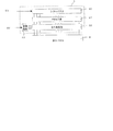
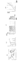
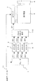
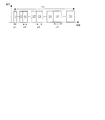
本発明の第1実施形態に係る画像表示装置の回路ブロック図を図1に示す。図において、11は入力信号端子、1はデコーダ、2〜5はカウンタ、6は電圧設定部、7はXドライバ、8はYドライバ、9は表示パネルである。ここで、デコーダ1及びカウンタ2〜5によって明るさ評価回路が構成され、電圧設定部6によって入出力変換特性偏向回路が構成される。また、電圧設定部6及びXドライバによって駆動回路が構成され、表示パネル9によって表示部が構成される。
<
FIG. 1 shows a circuit block diagram of the image display apparatus according to the first embodiment of the present invention. In the figure, 11 is an input signal terminal, 1 is a decoder, 2 to 5 are counters, 6 is a voltage setting unit, 7 is an X driver, 8 is a Y driver, and 9 is a display panel. Here, a brightness evaluation circuit is configured by the
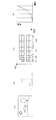
表示パネル9には複数の発光素子がマトリクス状に配列され、線順次駆動により駆動される。表示素子である発光素子としては、電子放出素子によるもの(電子放出素子と蛍光体との組合せ)、特には電子放出素子として冷陰極素子を用いたもの、あるいは、エレクトロルミネッセンス素子、プラズマ表示素子、液晶素子等を用いることができる。
A plurality of light emitting elements are arranged in a matrix on the
図2は図1のXドライバ7の一例を示した図である。図中で20はシフトレジスタ、21はPWM回路、22は出力段回路、23は電源回路である。ここでPWM回路21と出力
段回路22が変調回路を構成する。またデコーダ1、カウンタ2から5、電圧設定回路6、電源回路23が制御回路を構成する。
FIG. 2 is a diagram showing an example of the
入力された画像データS0はシフトレジスタ20に入力され、シリアル−パラレル変換される。シフトレジスタ20では、一行分の画像データをシリアル−パラレル変換し、PWM回路21に出力する。
The input image data S0 is input to the
PWM回路21にはラッチ回路があり、シフトレジスタから出力された一行分の画像データを一水平同期期間(以下1Hと呼ぶ)保持する。PWM回路21では、一行分のデータをパルス幅変調信号(以下PWM信号と呼ぶ)に変換する。
The
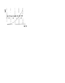
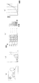
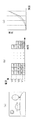
本実施形態では、パルス幅変調優先型多値PWMを想定している。パルス幅変調優先型多値PWMの説明図を図3に示す。図3では、画像データが0〜255の8ビットデータであった場合、表示パネルの一発光素子に印加される電圧波形を示している。図の横軸は時間を、縦軸は発光素子に印加する電圧をあらわしている。 In the present embodiment, pulse width modulation priority type multi-level PWM is assumed. An explanatory diagram of the pulse width modulation priority type multi-value PWM is shown in FIG. FIG. 3 shows a voltage waveform applied to one light-emitting element of the display panel when the image data is 8-bit data of 0 to 255. In the figure, the horizontal axis represents time, and the vertical axis represents the voltage applied to the light emitting element.
図3(a)に示すように、本実施形態では変調回路から発光素子に印加される電位は4値(V1、V2、V3、V4)あることを想定している。変調回路から印加される電位と走査回路であるYドライバ8から印加される選択信号の電位との電位差が、変調配線と走
査配線とを介して各素子に駆動電圧として印加される。なおここでは選択信号の電位が0ボルトである構成を採用している。図3(a)は画像データが255であった場合の電圧波形である。図に示すように、画像データが255の場合は、63スロットまでは電圧V4が発光素子に印加され、64スロット目のみ電圧V3が印加される。
As shown in FIG. 3A, in this embodiment, it is assumed that the potential applied from the modulation circuit to the light emitting element has four values (V1, V2, V3, V4). A potential difference between the potential applied from the modulation circuit and the potential of the selection signal applied from the
画像データが63であった場合の電圧波形を図3(b)に示す。このように、画像データが0〜64の間であれば、電圧はV1で固定となり画像データに応じてパルス幅変調される。 A voltage waveform when the image data is 63 is shown in FIG. Thus, if the image data is between 0 and 64, the voltage is fixed at V1 and is pulse width modulated according to the image data.
画像データが66であった場合の電圧波形を図3(c)に示す。図に示すように画像データが66の場合は、2スロットまでは電圧V2が発光素子に印加され、その後3スロット目からはV1が印加される。 A voltage waveform when the image data is 66 is shown in FIG. As shown in the figure, when the image data is 66, the voltage V2 is applied to the light emitting element up to the second slot, and then V1 is applied from the third slot.
このように本実施形態のパルス幅優先型多値PWMは、階調を0〜64、65〜128、129〜192、193〜255の4ブロック(4つのサブ範囲)に分割し、各階調ブロックは発光素子に印加する最大電圧が異なり、また各階調ブロック内ではパルス幅変調する(各階調ブロック内では最大電圧の部分が階調値の増加に伴って順次長くなる)電圧
波形となっている。
As described above, the pulse width priority type multi-value PWM according to the present embodiment divides the gradation into four blocks (four sub-ranges) of 0 to 64, 65 to 128, 129 to 192, and 193 to 255. The maximum voltage applied to the light emitting element is different, and the voltage waveform is pulse-width modulated in each gradation block (the maximum voltage portion is gradually increased as the gradation value increases in each gradation block).
本実施形態では4値のパルス幅変調優先型多値PWMを想定しており、PWM回路21の出力は各電位値V1〜V4に対するPWM信号である。従って、PWM回路21の一つの出力端子からは、V1〜V4それぞれに対応する4つのPWM信号が出力されることになる。ここで、電位V1〜V4がそれぞれ振幅設定用信号に相当する。
In this embodiment, a 4-value pulse width modulation priority type multi-value PWM is assumed, and the output of the
PWM回路21から出力されるPWM信号は出力段回路22に入力される。出力段回路22では、V1〜V4の各電位値に対応するPWM信号により指定された期間、各電位を表示パネルの変調配線に出力する。
The PWM signal output from the
電源回路23はV1〜V4に対応するの4つの電源部を持ち、V1〜V4の電位をパルス信号の振幅を設定するための基準信号として出力段回路22に供給している。電源回路23には電位設定信号SVが入力されており、電位設定値SVにより4つの電源部からの出力値に対するゲインをコントロールし、出力電位であるV1からV4を調整している。電位設定信号SVの詳細は後述する。
The
図3の電圧波形により発光素子を駆動したときの階調輝度特性を図4に示す。図4の横軸は階調、つまり画像データを、縦軸は輝度(明るさ)を表している。パルス幅変調優先型多値PWMの場合、図に示すように階調が4ブロックに分かれ、各ブロックで直線的に輝度が変化するような特性となる。ここでは、各階調ブロックを図のようにA、B、C、Dとする。Aブロックは階調0〜64のブロックで、このデータが入力されると電圧V1で発光素子を駆動する。Bブロックは階調65〜128のブロックで、このデータが入力されると電圧V2あるいはV1で発光素子を駆動する。Cブロックは階調129〜192のブロックで、このデータが入力されると電圧V3あるいはV2で発光素子を駆動する。Dブロックは階調193〜255のブロックで、このデータが入力されると電圧V4あるいはV3で発光素子を駆動する。
FIG. 4 shows gradation luminance characteristics when the light emitting element is driven by the voltage waveform of FIG. The horizontal axis of FIG. 4 represents gradation, that is, image data, and the vertical axis represents luminance (brightness). In the case of pulse width modulation priority type multi-value PWM, as shown in the figure, the gradation is divided into four blocks, and the luminance changes linearly in each block. Here, each gradation block is A, B, C, and D as shown in the figure. The A block is a block of
A、B、C、Dの各階調ブロック内では単純なパルス幅変調と等価であるため、階調輝度特性は直線となる。従って、0〜255の全階調の特性は図4に示すように折れ線状になる。 Since each of the A, B, C, and D gradation blocks is equivalent to simple pulse width modulation, the gradation luminance characteristic is a straight line. Therefore, the characteristics of all gradations from 0 to 255 are broken lines as shown in FIG.
また、図3ではV1−0=V2−V1=V3−V2=V4−V3、ここで黒レベルは0ボルトである、と設定した場合を示しており(電圧等分割)、このとき図4に示すように標準的なγ特性(例えばγ=2.2)の近似折れ線が得られるものとする。仮に、V1のみを大きくすると、階調ブロックAの階調輝度特性の傾きが大きくなり、逆にV1のみ小さくすると階調ブロックAの傾きが小さくなる。このように、本実施形態では、電圧V1〜V4を制御することで、各階調ブロックの階調輝度特性の傾きを変えることができる。 FIG. 3 shows a case where V1-0 = V2-V1 = V3-V2 = V4-V3, where the black level is set to 0 volts (voltage equal division). As shown, an approximate broken line having a standard γ characteristic (for example, γ = 2.2) is assumed to be obtained. If only V1 is increased, the gradient of the gradation luminance characteristic of the gradation block A is increased. Conversely, if only V1 is decreased, the gradient of the gradation block A is decreased. Thus, in this embodiment, the gradient of the gradation luminance characteristic of each gradation block can be changed by controlling the voltages V1 to V4.
次に図1を用いて本実施形態のγ補正法について説明する。 Next, the γ correction method of this embodiment will be described with reference to FIG.
入力端子11に入力された画像データはAD変換された8ビットのデータであるとする。この8ビットの画像データは上位2ビットがデコーダ1に入力される。デコーダ1では、00、01、10、11の2ビットデータを4ビットの信号SC1〜SC4に変換し、カウンタ2、3、4、5に出力する。
It is assumed that the image data input to the
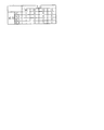
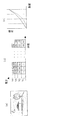
図5はデコーダ1の入出力を示したものである。デコーダ1の入力は、00、01、10、11の2ビットデータであり、出力は、SC1、SC2、SC3、SC4の4ビットデータである。SC1はカウンタ2に、SC2はカウンタ3に、SC3はカウンタ4に、SC4はカウンタ5にそれぞれ入力される。
FIG. 5 shows the input / output of the
カウンタ2、3、4、5では、デコーダ1により出力された4ビットの信号SC1〜SC4をカウントし、累積ヒストグラムSH1〜SH4を生成する。つまり、カウンタ2は画像データ0〜63の度数をカウントし、カウンタ3は画像データ0〜127の度数をカウントし、カウンタ4は画像データ0〜191の度数をカウントし、カウンタ5は画像データ0〜255の度数をカウントする。
The
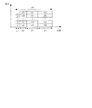
図6は電圧設定部6の詳細図である。カウンタ2〜4によりカウントされた累積ヒストグラムデータSH1〜SH4は、メモリ50〜53に随時更新しながら格納される。1フレーム分の画像データの累積ヒストグラムカウントが終了した時点で、メモリ50〜53には制御信号Syncが入力され、メモリされているデータを出力するとともにメモリは0にリセットされる。これにより、メモリ50〜53は1フレーム分の累積ヒストグラムデータを出力する。これが1フレーム分の画像信号に対応する特性データを構成する。なお、この特性データは1フレーム分の画像信号によって求める構成に限るものではなく、例えばフィールド単位で画像が形成される場合には1フィールド分の画像信号に基づいて求めてもよく、また数フィールド分もしくは数フレーム分の画像信号に基づいて求めてもよい。
FIG. 6 is a detailed view of the
ここで、メモリ53の出力は画像データ0〜255の累積ヒストグラムであり、これは画像データの全画素数と一致する。
Here, the output of the
本実施形態では、説明のためカウンタ5により0〜255の累積ヒストグラムをカウントする構成を示したが、実際には0〜255の累積ヒストグラムを1フレーム分カウントすると全画素数と一致するため、カウンタ5、メモリ53はなくてもよい。
In the present embodiment, the configuration in which the cumulative histogram from 0 to 255 is counted by the
メモリ50〜53から出力された累積ヒストグラムデータはゲインがかけられ、電圧設定信号SV1、SV2、SV3、SV4となって電源回路に出力される。従って累積ヒストグラムSH1〜SH4と電圧設定信号SV1〜SV4の関係は、SH1が大きいほどSV1は大きくなり、SH2が大きいほどSV2は大きくなり、SH3が大きいほどSV3は大きくなり、SH4が大きいほどSV4が大きくなる。このとき、明るさ調整やコントラスト調整等の情報を加味してゲイン設定を行う方法としても良い。 The accumulated histogram data output from the memories 50 to 53 is gained and is output to the power supply circuit as voltage setting signals SV1, SV2, SV3, SV4. Therefore, the relationship between the cumulative histograms SH1 to SH4 and the voltage setting signals SV1 to SV4 indicates that SV1 increases as SH1 increases, SV2 increases as SH2 increases, SV3 increases as SH3 increases, and SV4 increases as SH4 increases. growing. At this time, the gain setting may be performed in consideration of information such as brightness adjustment and contrast adjustment.
電圧設定信号SV1、SV2、SV3、SV4はそれぞれ、電源回路においてV1、V2、V3、V4の電位値を制御する。このとき、SV1が大きいほどV1を大きく、SV2が大きいほどV2を大きく、SV3が大きいほどV3を大きく、SV4が大きいほどV4を大きくなるように各電位が制御される。 Voltage setting signals SV1, SV2, SV3, and SV4 control the potential values of V1, V2, V3, and V4 in the power supply circuit, respectively. At this time, each potential is controlled such that V1 is increased as SV1 is increased, V2 is increased as SV2 is increased, V3 is increased as SV3 is increased, and V4 is increased as SV4 is increased.
本実施形態の表示法によれば、V1が大きくなると図4の階調ブロックAの階調輝度特性の傾きが大きくなり、V2が大きくなると階調ブロックBの傾きが大きくなり、V3が大きくなると階調ブロックCの傾きが大きくなり、V4が大きくなると階調ブロックDの傾きが大きくなる。 According to the display method of this embodiment, when V1 increases, the gradient of the gradation luminance characteristic of the gradation block A in FIG. 4 increases, and when V2 increases, the gradient of the gradation block B increases and V3 increases. The gradient of the gradation block C increases, and as V4 increases, the gradient of the gradation block D increases.
本実施形態では、電圧設定信号SV1〜SV4を電位V1〜V4の値を制御する信号として用いたが、別の構成としては、電圧設定信号SV1〜SV4をDA変換し、このDA変換された信号をそのままV1〜V4電位として使用するようにしてもよい。すなわち、変調回路が出力するパルス信号の振幅を設定する際の基準信号となる振幅設定用信号であるV1からV4のそれぞれが、特性データに応じて設定できる種々の構成を採用できる。 In the present embodiment, the voltage setting signals SV1 to SV4 are used as signals for controlling the values of the potentials V1 to V4. However, as another configuration, the voltage setting signals SV1 to SV4 are DA-converted and the DA-converted signals are used. May be used as the potentials V1 to V4 as they are. That is, it is possible to employ various configurations in which each of the amplitude setting signals V1 to V4 serving as a reference signal when setting the amplitude of the pulse signal output from the modulation circuit can be set according to the characteristic data.
次にγ補正の処理過程を図7、8を用いて説明する。 Next, the process of γ correction will be described with reference to FIGS.
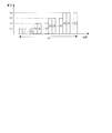
図7は暗い画像が入力されたときの処理例である。図7(a)は入力画像を示している。図7(b)において、破線は入力画像である図7(a)のヒストグラムを、棒グラフはその累積ヒストグラムを表している。累積ヒストグラムは図6のメモリ50〜53の出力である。 FIG. 7 shows an example of processing when a dark image is input. FIG. 7A shows an input image. In FIG. 7B, the broken line represents the histogram of FIG. 7A, which is an input image, and the bar graph represents the cumulative histogram. The cumulative histogram is the output of the memories 50 to 53 in FIG.
電圧設定部6において累積ヒストグラムデータは電圧設定信号SV1〜SV4に変換される。この電圧設定信号により電源回路は電位V1〜V4を指示された値に設定する。
In the
例えば図7(a)のように暗い画像が入力された場合、ヒストグラムは図7(b)の破線のようになり、累積ヒストグラムは図7(b)の棒グラフのようになる。つまり、暗い階調ほど累積ヒストグラムの増加量が大きいことになる。このような場合、発光素子に印加する電圧波形は図7(c)のように、V1−0、V2−V1が図3(a)より大きく、V3−V2、V4−V3が図3(a)より小さい波形となる。 For example, when a dark image is input as shown in FIG. 7A, the histogram is as shown by a broken line in FIG. 7B, and the cumulative histogram is as shown in a bar graph in FIG. 7B. That is, the darker gradation has a larger increase amount of the cumulative histogram. In such a case, as shown in FIG. 7C, the voltage waveforms applied to the light emitting elements are such that V1-0 and V2-V1 are larger than those in FIG. 3A, and V3-V2 and V4-V3 are in FIG. ) Smaller waveform.
このような電圧波形で発光素子を駆動した場合、発光素子の階調輝度特性は図7(d)のようになる。つまり、暗い階調ほどコントラストをつけるような特性となる。図7(d)の破線は標準の状態の(例えばγ=2.2となる)階調輝度特性である。 When the light emitting element is driven with such a voltage waveform, the gradation luminance characteristic of the light emitting element is as shown in FIG. In other words, the dark gradation has the characteristic of giving contrast. A broken line in FIG. 7D is a gradation luminance characteristic in a standard state (for example, γ = 2.2).
図8は明るい画像が入力されたときの処理例である。図8(a)は入力画像を示している。図7同様、図8(b)において破線はヒストグラムを、棒グラフは累積ヒストグラムを表している。 FIG. 8 shows an example of processing when a bright image is input. FIG. 8A shows an input image. As in FIG. 7, the broken line in FIG. 8B represents the histogram, and the bar graph represents the cumulative histogram.
図8(a)のように明るい画像が入力された場合、ヒストグラムは図8(b)の破線のようになり、累積ヒストグラムは図8(b)の棒グラフのようになる。つまり、明るい階調ほど累積ヒストグラムの増加量が大きいことになる。このような場合、発光素子に印加する電圧波形は図8(c)のように、V1−0、V2−V1が図3(a)より小さく、V3−V2、V4−V3が図3(a)より大きい波形となる。 When a bright image is input as shown in FIG. 8A, the histogram is as shown by the broken line in FIG. 8B, and the cumulative histogram is as shown in the bar graph in FIG. 8B. In other words, the amount of increase in the cumulative histogram increases as the gradation becomes brighter. In such a case, as shown in FIG. 8C, the voltage waveforms applied to the light emitting elements are such that V1-0 and V2-V1 are smaller than those in FIG. 3A, and V3-V2 and V4-V3 are in FIG. ) Larger waveform.
このような電圧波形で発光素子を駆動した場合、発光素子の階調輝度特性は図8(d)のようになる。つまり、明るい階調ほどコントラストをつけるような特性となる。 When the light emitting element is driven with such a voltage waveform, the gradation luminance characteristic of the light emitting element is as shown in FIG. In other words, the brighter gradation has the characteristic of giving contrast.
このように、累積ヒストグラムの増加量が大きい階調ブロックにコントラストをつけることにより、入力画像に適応し常に良好なコントラストで表示することが可能である。 In this way, by applying contrast to a gradation block in which the amount of increase in the cumulative histogram is large, it is possible to adapt to the input image and always display with good contrast.
以上のように本発明を適用すれば、γ補正の際γテーブルを用いる必要がなく回路量を小さく抑えることができる。また、電圧というアナログ手法によりγ補正するため階調つぶれも発生しない。最大振幅がV1となるパルス信号に対応する階調範囲と、最大振幅がV2になるパルス信号に対応する階調範囲と、最大振幅がV3となるパルス信号に対応する階調範囲と、最大振幅がV4になるパルス信号に対応する階調範囲と、がそれぞれ、ヒストグラムをカウントするサブ範囲と一致する構成を特に好適な例としてここでは示した。この階調範囲とサブ範囲とは必ずしも一致させる必要はないが、その場合は別途デジタル信号処理を行うなどによって各階調範囲間での表示状態の不連続性を少なくするようにするとよい。その場合であっても、本願発明を採用しない場合と比べてデジタル信号処理による階調の減少を抑制することができる。 If the present invention is applied as described above, it is not necessary to use a γ table for γ correction, and the circuit amount can be reduced. Further, since the γ correction is performed by an analog method called voltage, gradation collapse does not occur. The gradation range corresponding to the pulse signal with the maximum amplitude V1, the gradation range corresponding to the pulse signal with the maximum amplitude V2, the gradation range corresponding to the pulse signal with the maximum amplitude V3, and the maximum amplitude Here, a configuration in which the gradation range corresponding to the pulse signal in which V becomes V4 and the sub-range in which the histogram is counted is shown as a particularly preferable example. The gradation range and the sub-range do not necessarily need to coincide with each other, but in that case, discontinuity of the display state between the gradation ranges may be reduced by separately performing digital signal processing or the like. Even in such a case, it is possible to suppress a decrease in gradation due to digital signal processing as compared with a case where the present invention is not adopted.
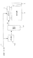
<実施形態2>パルス幅変調優先型多値PWM
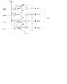
本発明の第2実施形態に係る画像表示装置の回路ブロック図を図9に示す。図1と同じ符号は同じものを表している。100はAPL検出部、101は電圧設定部である。ここで、APL検出部100によって画像の明るさを評価する明るさ評価回路が構成される。
<
FIG. 9 shows a circuit block diagram of an image display apparatus according to the second embodiment of the present invention. The same reference numerals as those in FIG. 1 denote the same components.
APL検出部100は画像データ1フレーム分のAPL(平均画像レベル :Average Picture Level)を検出する。検出されたAPLは電圧設定部101に入力される。
The
電圧設定部101には不図示のROMがあり、このROMはAPLをアドレスとして、電圧設定値SV1、SV2、SV3、SV4を出力する。Xドライバ7内の電源回路は、電圧設定値SV1〜SV4により設定された電位V1〜V4を出力し、この電位を用いて発光素子を駆動する。ここで、V1〜V4が振幅設定用信号に相当する。
The
次に、γ補正の処理例を図10、図11を用いて説明する。 Next, an example of γ correction processing will be described with reference to FIGS.
図10は暗い画像が入力された場合のγ補正処理例である。図10(a)のように暗い画像の場合APLは低い値となる。電圧設定部101では、入力されたAPLをアドレスとして4つの電圧設定値SV1〜SV4を出力する。Xドライバ7内の電源回路では、電圧設定値SV1〜SV4によりV1〜V4を設定する。
FIG. 10 shows an example of γ correction processing when a dark image is input. In the case of a dark image as shown in FIG. 10A, APL is a low value. The
図10(a)のように暗い画像の場合、発光素子に印加する電圧波形は図10(b)のように、V1−0、V2−V1が図3(a)より大きく、V3−V2、V4−V3が図3(a)より小さい波形となる。その結果、発光素子の階調輝度特性は図10(c)に示すようになる。すなわち、中間値近傍(階調値128)よりも低い階調領域において、特性線の傾きがおおきくなって、暗い階調ほどコントラストをつけるような特性となる。 In the case of a dark image as shown in FIG. 10A, the voltage waveforms applied to the light emitting elements are V1-0 and V2-V1 larger than those shown in FIG. 3A as shown in FIG. V4-V3 has a smaller waveform than FIG. As a result, the gradation luminance characteristic of the light emitting element is as shown in FIG. That is, in the gradation region lower than the vicinity of the intermediate value (gradation value 128), the characteristic line has a large slope, and the dark gradation has the characteristic of giving contrast.
図11は明るい画像が入力された場合のγ補正処理例である。図11(a)のように明るい画像の場合APLは高い値となる。 FIG. 11 shows an example of γ correction processing when a bright image is input. In the case of a bright image as shown in FIG. 11A, APL has a high value.
このように明るい画像の場合、発光素子に印加する電圧波形は図11(b)のように、V1−0、V2−V1が図3(a)より小さく、V3−V2、V4−V3が図3(a)より大きい波形となる。その結果、発光素子の階調輝度特性は図11(c)のようになる。すなわち中間値近傍よりも高い階調領域において、特性線の傾きが大きくなるように変更され、明るい階調ほどコントラストをつけるような特性となる。 In such a bright image, as shown in FIG. 11B, the voltage waveforms applied to the light emitting elements are such that V1-0 and V2-V1 are smaller than those in FIG. 3A, and V3-V2 and V4-V3 are illustrated. The waveform is larger than 3 (a). As a result, the gradation luminance characteristic of the light emitting element is as shown in FIG. That is, in the gradation region higher than the vicinity of the intermediate value, the characteristic line is changed so that the inclination of the characteristic line becomes larger, and the contrast becomes higher as the gradation becomes brighter.
このように、入力画像に適応し常に良好なコントラストで表示することが可能である。 In this way, it is possible to adapt to the input image and always display with good contrast.
以上のように本発明によれば、γ補正の際γテーブルを用いる必要がなく回路量を小さく抑えることができる。また、電圧というアナログ手法によりγ補正するため階調つぶれも発生しない。 As described above, according to the present invention, it is not necessary to use a γ table for γ correction, and the circuit amount can be reduced. Further, since the γ correction is performed by an analog method called voltage, gradation collapse does not occur.
<実施形態3>電圧変調優先型多値PWM
本発明の第3実施形態に係る画像表示装置の回路ブロック図を図12に示す。図12において、図1と同じ符号のブロックは同じものを表している。110はPWMクロック設定部である。ここで、PWMクロック設定部110によって入出力変換特性変更回路が構成され、PWMクロック設定部110及びXドライバ7によって駆動回路が構成される。
<Third embodiment> Voltage modulation priority type multi-value PWM
FIG. 12 shows a circuit block diagram of an image display apparatus according to the third embodiment of the present invention. 12, blocks having the same reference numerals as those in FIG. 1 represent the same components.
図13は本実施形態の駆動法により8ビット画像データを表示する際の電圧波形を示している。本実施形態では図に示すような電圧(振幅)変調優先型多値PWMを想定している。本実施形態では1Hを4スロットに分割し、最初のスロットをパルス幅p1で、2番目のスロットをパルス幅p2で、3番目のスロットをパルス幅p3で、最後のスロットをパルス幅p4で駆動する。各スロット(階調ブロック)内では、電圧(振幅)変調により階調表現を行っている。このように駆動することにより、発光素子は図4のような標準的
な(例えばγ=2.2であるような)階調輝度特性を示す。
FIG. 13 shows voltage waveforms when displaying 8-bit image data by the driving method of this embodiment. In this embodiment, voltage (amplitude) modulation priority type multi-value PWM as shown in the figure is assumed. In this embodiment, 1H is divided into 4 slots, the first slot is driven with pulse width p1, the second slot is driven with pulse width p2, the third slot is driven with pulse width p3, and the last slot is driven with pulse width p4. To do. In each slot (gradation block), gradation expression is performed by voltage (amplitude) modulation. By driving in this way, the light emitting element exhibits a standard gradation luminance characteristic as shown in FIG. 4 (for example, γ = 2.2).
次に図12を用いて、本実施形態の動作を説明する。入力端子11に入力された画像データはAD変換された8ビットのデータであるとする。8ビットの画像データは上位2ビットがデコーダ1に入力される。デコーダ1では、00、01、10、11の2ビットデータを4ビットの信号SC1〜SC4に変換し、カウンタ2、3、4、5に出力する。
Next, the operation of this embodiment will be described with reference to FIG. It is assumed that the image data input to the
図14はデコーダ1の入出力を示したものである。デコーダ1の入力は、00、01、10、11の2ビットデータであり、出力は、SC1、SC2、SC3、SC4の4ビットデータである。SC1はカウンタ2に、SC2はカウンタ3に、SC3はカウンタ4に、SC4はカウンタ5にそれぞれ入力される。
FIG. 14 shows the input / output of the
カウンタ2、3、4、5はデコーダ1の出力をカウントし、ヒストグラムSH1〜SH4を生成する。
カウントされたヒストグラムSH1〜SH4はPWMクロック設定部110に入力される。PWMクロック設定部110はヒストグラムSH1〜SH4により、パルス幅p1〜p4を制御するためのPWMクロック設定信号SPをXドライバ7に出力する。ここで、パルス幅p1〜p4を設定するための信号が、パルス信号の時間幅を設定するための基準信号となる時間幅設定用信号に相当する。
The counted histograms SH <b> 1 to SH <b> 4 are input to the PWM
このとき、PWMクロック設定部110はSH1が大きいほどp1を長く、SH2が大きいほどp2を長く、SH3が大きいほどp3を長く、SH4が大きいほどp4を長く設定するようなPWMクロック設定信号SPを生成する。
At this time, the PWM
Xドライバ7内にはPWM回路があり、PWMクロック設定信号SPによりパルス幅p1〜p4を設定する。Xドライバ7は設定されたパルス幅p1〜p4に基づいて駆動電圧波形を生成し発光素子を駆動する。
There is a PWM circuit in the
次にγ補正の処理例を図15、16を用いて説明する。 Next, an example of γ correction processing will be described with reference to FIGS.
図15は暗い画像が入力された場合の処理例である。図15(a)は入力画像である。デコーダ1、カウンタ2〜5により図15(a)のヒストグラムSH1〜SH4がカウントされる。図15(b)は図15(a)のヒストグラムである。
FIG. 15 shows a processing example when a dark image is input. FIG. 15A shows an input image. The
カウントされたヒストグラムデータSH1〜SH4はPWMクロック設定信号SPに変換される。Xドライバ内ではPWMクロック設定信号SPに基づいてパルス幅p1〜p4が設定される。 The counted histogram data SH1 to SH4 are converted into a PWM clock setting signal SP. In the X driver, pulse widths p1 to p4 are set based on the PWM clock setting signal SP.
図15(a)の画像が入力されたときの発光素子に印加される電圧波形は図15(c)のようになる。図15(c)に示すように、図13と比べパルス幅p1、p2が長く、p3、p4が短い電圧波形となる。その結果、発光素子の階調輝度特性は図15(d)に示すようになる。つまり、暗い階調ほどコントラストをつけるような特性となる。 The voltage waveform applied to the light emitting element when the image of FIG. 15A is input is as shown in FIG. As shown in FIG. 15C, the voltage waveforms are longer in the pulse widths p1 and p2 and shorter in p3 and p4 than in FIG. As a result, the gradation luminance characteristics of the light emitting element are as shown in FIG. In other words, the dark gradation has the characteristic of giving contrast.
図16は明るい画像が入力された場合の処理例である。図16(a)は入力画像、図16(b)はそのヒストグラムである。PWMクロック設定部110は、入力されたヒストグラムデータSH1〜SH4よりPWMクロック設定信号SPをXドライバ7に出力する。Xドライバ7では、PWMクロック設定信号SPによりパルス幅p1〜p4が設定される。
FIG. 16 shows an example of processing when a bright image is input. FIG. 16A is an input image, and FIG. 16B is a histogram thereof. The PWM
図16(a)の画像が入力されたときの発光素子に印加される電圧波形は図16(c)のようになる。図16(c)に示すように、図13と比べパルス幅p1、p2が短く、p3、p4が長い電圧波形となる。その結果、発光素子の階調輝度特性は図16(d)に示すようになる。つまり、明るい階調ほどコントラストをつけるような特性となる。 The voltage waveform applied to the light emitting element when the image of FIG. 16A is input is as shown in FIG. As shown in FIG. 16C, the voltage waveforms are shorter in the pulse widths p1 and p2 and longer in p3 and p4 than in FIG. As a result, the gradation luminance characteristics of the light emitting element are as shown in FIG. In other words, the brighter gradation has the characteristic of giving contrast.
このように、ヒストグラムの大きい階調ブロックにコントラストをつけることにより、入力画像に適応し常に良好なコントラストで表示することが可能である。 In this way, by giving contrast to a gradation block having a large histogram, it is possible to adapt to the input image and always display with good contrast.
以上のように本発明を適用すれば、γ補正の際γテーブルを用いる必要がなく回路量を小さく抑えることができる。また、デジタルデータの変換を行わないためγ補正による階調つぶれも発生しない。 If the present invention is applied as described above, it is not necessary to use a γ table for γ correction, and the circuit amount can be reduced. Further, since digital data is not converted, gradation collapse due to γ correction does not occur.
<参考形態>PWM
参考形態として、電圧固定のPWMで駆動した場合のγ補正を説明する。本参考形態の回路ブロック図は実施形態3同様図12である。
<Reference form> PWM
As a reference form, γ correction when driven by voltage-fixed PWM will be described. The circuit block diagram of this reference embodiment is FIG. 12 as in the third embodiment.
図17は本参考形態の駆動電圧波形である。本参考形態は階調を0〜63、64〜127、128〜191、192〜255の4つのブロックに分割し、各階調ブロックでパルス幅が異なるような電圧波形を有する。階調0〜63の1スロットのパルス幅をp1、階調64〜127の1スロットのパルス幅をp2、階調128〜191の1スロットのパルス幅をp3、階調192〜255の1スロットのパルス幅をp4とする。
FIG. 17 shows a drive voltage waveform of this reference embodiment. In this reference embodiment, the gradation is divided into four blocks of 0 to 63, 64 to 127, 128 to 191 and 192 to 255, and each gradation block has a voltage waveform with a different pulse width. The pulse width of 1 slot of
ここで、標準的な状態ではp1〜p4は図17に示すようになっており、このとき発光素子の階調輝度特性は図3のような標準的な特性(例えばγ=2.2)となる。 Here, in a standard state, p1 to p4 are as shown in FIG. 17, and at this time, the gradation luminance characteristic of the light emitting element is a standard characteristic (for example, γ = 2.2) as shown in FIG. Become.
次に、図12を用いて本参考形態の動作を説明する。 Next, the operation of the present embodiment will be described with reference to FIG.
実施形態3と同様に、画像データの上位2ビットによりヒストグラムをとりSH1〜SH4がPWMクロック設定部110に入力される。PWMクロック設定部110はヒストグラムSH1〜SH4によりパルス幅p1〜p4を制御するためのPWMクロック設定信号SPをXドライバ7に出力する。ここで、パルス幅p1〜p4が駆動信号波形パラメータに相当する。
As in the third embodiment, a histogram is taken with the upper 2 bits of the image data, and SH1 to SH4 are input to the PWM
このとき、PWMクロック設定部110はSH1が大きいほどp1を長く、SH2が大きいほどp2を長く、SH3が大きいほどp3を長く、SH4が大きいほどp4を長く設定するようなPWMクロック設定信号SPを生成する。
At this time, the PWM
Xドライバ7内には不図示のPWM回路があり、PWMクロック設定信号SPによりパルス幅p1〜p4を設定する。Xドライバ7は設定されたパルス幅p1〜p4に基づいて駆動電圧波形を生成し発光素子を駆動する。
There is a PWM circuit (not shown) in the
このように駆動することで実施形態3同様、ヒストグラムの大きい階調ブロックにコントラストをつけることにより、入力画像に適応し常に良好なコントラストで表示することが可能である。しかしながら、充分な階調数をこの構成で得るためには、充分に早いパルス幅変調用のクロック信号を実現する必要がある。 By driving in this way, as in the third embodiment, it is possible to adapt to the input image and always display with good contrast by giving contrast to the gradation block having a large histogram. However, in order to obtain a sufficient number of gradations with this configuration, it is necessary to realize a sufficiently fast clock signal for pulse width modulation.
<実施形態4>パルス幅変調優先型多値PWM(並置型)
本発明の第4実施形態として、図18に示す電圧波形により発光素子を駆動する例を説明する。
<
As a fourth embodiment of the present invention, an example in which a light emitting element is driven with a voltage waveform shown in FIG. 18 will be described.
本実施形態では、階調を0〜63、64〜127、128〜191、192〜255の4つのブロックに分割し、各階調ブロックで電圧が異なるような電圧波形を有する。また、各階調ブロックにおいて、1スロットのパルス幅は均一であるとする。図18は、V1−0=V2−V1=V3−V2=V4−V3と設定した場合を示しており(電圧等分割)、このとき図4に示すように標準的なγ特性(例えばγ=2.2)の近似折れ線が得られるものとする。 In the present embodiment, the gradation is divided into four blocks of 0 to 63, 64 to 127, 128 to 191 and 192 to 255, and each gradation block has a voltage waveform with a different voltage. In each gradation block, the pulse width of one slot is assumed to be uniform. FIG. 18 shows a case where V1-0 = V2-V1 = V3-V2 = V4-V3 (voltage equal division). At this time, as shown in FIG. 4, a standard γ characteristic (for example, γ = It is assumed that the approximate broken line of 2.2) is obtained.
本実施形態の駆動ブロック図は図1である。実施形態1では、デコーダ1とカウンタ2〜5により累積ヒストグラムをカウントしたが、本実施形態ではヒストグラムをカウントする。この場合、デコーダ1の入出力は図14のようになる。
The drive block diagram of this embodiment is shown in FIG. In the first embodiment, the cumulative histogram is counted by the
カウントされたヒストグラムは電圧設定部6で電圧設定信号SVに変換され、Xドライバ7内で電位値V1〜V4を設定し駆動波形を作る。このとき、ヒストグラムSH1が大きいときはV1が大きく、SH2が大きいときはV2が大きく、SH3が大きいときはV3が大きく、SH4が大きいときはV4が大きくなるように電位値V1〜V4が設定される。ここで、電位値V1〜V4が駆動信号波形パラメータに相当する。
The counted histogram is converted into a voltage setting signal SV by the
このように駆動することで、ヒストグラムの大きい階調ブロックにコントラストをつけることにより、入力画像に適応し常に良好なコントラストで表示することが可能である。 By driving in this way, it is possible to adapt to the input image and always display with good contrast by giving contrast to the gradation block having a large histogram.
以上のように本発明を適用すれば、γ補正の際γテーブルを用いる必要がなく回路量を小さく抑えることができる。また、デジタルデータの変換を行わないためγ補正による階調つぶれも発生しない。 If the present invention is applied as described above, it is not necessary to use a γ table for γ correction, and the circuit amount can be reduced. Further, since digital data is not converted, gradation collapse due to γ correction does not occur.
1 デコーダ
2、3、4、5カウンタ
6 電圧設定部
7 Xドライバ
8 Yドライバ
9 表示パネル
11 入力端子
20 シフトレジスタ
21 PWM回路
22 出力段回路
23 電源回路
50、51、52、53 メモリ
100 APL検出部
101 電圧設定部
110 PWMクロック設定部
DESCRIPTION OF
Claims (11)
該変調回路において用いる振幅設定用信号及び/もしくは時間幅設定用信号であって、前記変調回路において画像信号の階調値に基づいて出力するパルス信号の振幅及び/もしくは時間幅を設定するのに用いる振幅設定用信号及び/もしくは時間幅設定用信号を、入力された画像信号の特性を示す特性データに基づいて設定する制御回路と、を有しており、
前記変調回路は、出力する前記パルス信号の時間幅と振幅とを前記階調値に対応させて設定するときの基準信号として前記時間幅設定用信号及び/もしくは前記振幅設定用信号を用いる回路である、
制御装置。 A modulation circuit;
An amplitude setting signal and / or time width setting signal used in the modulation circuit for setting the amplitude and / or time width of a pulse signal to be output based on the gradation value of the image signal in the modulation circuit. A control circuit that sets the amplitude setting signal and / or the time width setting signal to be used based on the characteristic data indicating the characteristics of the input image signal,
The modulation circuit is a circuit that uses the time width setting signal and / or the amplitude setting signal as a reference signal when setting the time width and amplitude of the pulse signal to be output in correspondence with the gradation value. is there,
Control device.
前記特性データは、
少なくとも1つの画像を形成するための複数の画像信号それぞれの階調値に基づいて該複数の画像信号を各サブ範囲毎に分けた時の、各サブ範囲毎の前記画像信号の密度を示すデータを有している請求項1に記載の制御装置。 A plurality of sub-ranges each constituting a part of a range of gradation values that can be taken by the image signal, a plurality of sub-ranges that do not completely overlap each other are set,
The characteristic data is
Data indicating the density of the image signal for each sub-range when the plurality of image signals are divided for each sub-range based on the gradation values of each of the plurality of image signals for forming at least one image The control device according to claim 1, comprising:
階調値を横軸にとり前記変調回路が出力するパルス信号によって駆動された画素が示す明るさを縦軸にとって示される階調対明るさ特性線の、前記第1のサブ範囲における傾きがより大きくなるように変更される請求項2に記載の制御装置。 The time width setting signal and / or the amplitude setting signal corresponding to a state in which the density has a predetermined value in a first sub-range which is one of the plurality of sub-ranges. In response to a state in which the density in the first sub-range is larger than the state in which the signal is set, the time width setting signal and / or the amplitude setting signal is changed. If
The gradient in the first sub-range of the gradation-brightness characteristic line indicated by the vertical axis is the brightness indicated by the pixel driven by the pulse signal output from the modulation circuit with the gray scale value on the horizontal axis. The control device according to claim 2, which is changed to become.
所定の階調範囲である第1の階調範囲において、順次に増やした階調値のそれぞれに対応させて、該第1の階調範囲に対応する最大振幅である第1の振幅を有する部分の時間幅を順次増やした前記パルス信号であって、前記第1の振幅となる部分以外に前記第1の階調範囲よりも低い階調範囲に対応する最大振幅となる部分を有する前記パルス信号をそれぞれ発生させ、
前記第1の階調範囲よりも高階調側の所定の階調範囲である第2の階調範囲において、順次に増やした階調値のそれぞれに対応させて、該第2の階調範囲に対応する最大振幅である第2の振幅を有する部分の時間幅を順次に増やした前記パルス信号であって、前記第2の振幅となる部分以外に前記第1の振幅となる部分を有する前記パルス信号をそれぞれ発生させる回路であり、
前記第1の振幅及び前記第2の振幅の少なくとも一方を前記特性データによって設定された前記振幅設定用信号を基準信号として設定する回路である請求項1乃至3のいずれかに記載の制御装置。 The modulation circuit includes:
A portion having a first amplitude that is the maximum amplitude corresponding to the first gradation range in a first gradation range that is a predetermined gradation range, corresponding to each of the gradation values that are sequentially increased. The pulse signal having the time width sequentially increased and having a portion having a maximum amplitude corresponding to a gradation range lower than the first gradation range in addition to the portion having the first amplitude. Respectively,
In the second gradation range, which is a predetermined gradation range on the higher gradation side than the first gradation range, the second gradation range corresponds to each of the sequentially increased gradation values. The pulse signal obtained by sequentially increasing the time width of the portion having the second amplitude that is the corresponding maximum amplitude, and having the portion that becomes the first amplitude in addition to the portion that becomes the second amplitude Each circuit generates a signal,
4. The control device according to claim 1, wherein the control device is a circuit that sets, as a reference signal, the amplitude setting signal in which at least one of the first amplitude and the second amplitude is set by the characteristic data. 5.
所定の階調範囲である第1の階調範囲において、順次に増やした階調値のそれぞれに対応させて、該第1の階調範囲に対応する最大振幅である第1の振幅を有する部分の時間幅を順次増やした前記パルス信号であって、前記第1の振幅となる部分以外に前記第1の階調範囲よりも低い階調範囲に対応する最大振幅となる部分を有する前記パルス信号をそれぞれ発生させ、
前記第1の階調範囲よりも高階調側の所定の階調範囲である第2の階調範囲において、順次に増やした階調値のそれぞれに対応させて、該第2の階調範囲に対応する最大振幅である第2の振幅を有する部分の時間幅を順次に増やした前記パルス信号であって、前記第2の振幅となる部分以外に前記第1の振幅となる部分を有する前記パルス信号をそれぞれ発生させる回路であり、
前記第1の振幅及び前記第2の振幅の少なくとも一方を前記特性データによって設定された前記振幅設定用信号を基準信号として設定する回路であり、
前記第1の階調範囲は前記複数のサブ範囲のうちの一つのサブ範囲に対応する階調範囲であり、前記第2の階調範囲は他の一つのサブ範囲に対応する階調範囲である請求項2もしくは3に記載の制御装置。 The modulation circuit includes:
A portion having a first amplitude that is the maximum amplitude corresponding to the first gradation range in a first gradation range that is a predetermined gradation range, corresponding to each of the gradation values that are sequentially increased. The pulse signal having the time width sequentially increased and having a portion having a maximum amplitude corresponding to a gradation range lower than the first gradation range in addition to the portion having the first amplitude. Respectively,
In the second gradation range, which is a predetermined gradation range on the higher gradation side than the first gradation range, the second gradation range corresponds to each of the sequentially increased gradation values. The pulse signal obtained by sequentially increasing the time width of the portion having the second amplitude that is the corresponding maximum amplitude, and having the portion that becomes the first amplitude in addition to the portion that becomes the second amplitude Each circuit generates a signal,
A circuit for setting, as a reference signal, the amplitude setting signal in which at least one of the first amplitude and the second amplitude is set by the characteristic data;
The first gradation range is a gradation range corresponding to one sub-range of the plurality of sub-ranges, and the second gradation range is a gradation range corresponding to one other sub-range. The control device according to claim 2 or 3.
前記特性データが前記第1の値とは異なる第2の値であって、前記特性データが前記第1の値となる画像よりも平均的な明るさが暗い画像に対応した値になった状態に対応して設定される前記時間幅設定用信号及び/もしくは振幅設定用信号は、
前記画像信号の取りうる階調値の範囲における中間値よりも低い階調領域の少なくとも一部において、階調値を横軸にとり前記変調回路が出力するパルス信号によって駆動された画素が示す明るさを縦軸にとって示される階調対明るさ特性線の傾きを前記第1の状態よりも大きくする値に設定される請求項6に記載の制御装置。 For the time width setting signal and / or the amplitude setting signal set corresponding to the first state in which the characteristic data has a first value,
The characteristic data is a second value different from the first value, and the characteristic data is a value corresponding to an image whose average brightness is darker than an image having the first value. The time width setting signal and / or the amplitude setting signal set corresponding to
Brightness indicated by pixels driven by a pulse signal output from the modulation circuit with the horizontal axis representing the gradation value in at least a part of the gradation region lower than the intermediate value in the gradation value range that the image signal can take The control device according to claim 6, wherein the control unit is set to a value that makes the gradient of the gradation vs. brightness characteristic line indicated by the vertical axis larger than that in the first state.
前記特性データが前記第1の値とは異なる第2の値であって、前記特性データが前記第1の値となる画像よりも平均的な明るさが明るい画像に対応した値になった状態に対応して設定される前記時間幅設定用信号及び/もしくは振幅設定用信号は、
前記画像信号の取りうる階調値の範囲における中間値よりも高い階調領域の少なくとも一部において、階調値を横軸にとり前記変調回路が出力するパルス信号によって駆動された画素が示す明るさを縦軸にとって示される階調対明るさ特性線の傾きを前記第1の状態よりも大きくする値に設定される請求項6に記載の制御装置。 For the time width setting signal and / or the amplitude setting signal set corresponding to the first state in which the characteristic data has a first value,
The characteristic data is a second value different from the first value, and the characteristic data is a value corresponding to an image whose average brightness is brighter than an image having the first value. The time width setting signal and / or the amplitude setting signal set corresponding to
Brightness indicated by pixels driven by a pulse signal output from the modulation circuit with the horizontal axis representing the gradation value in at least a part of the gradation region higher than the intermediate value in the range of gradation values that can be taken by the image signal The control device according to claim 6, wherein the control unit is set to a value that makes the gradient of the gradation vs. brightness characteristic line indicated by the vertical axis larger than that in the first state.
前記制御装置の前記変調回路が出力する前記パルス信号が印加される表示素子を有する表示器と、
を有する画像表示装置。 A control device according to any one of claims 1 to 8,
A display having a display element to which the pulse signal output from the modulation circuit of the control device is applied;
An image display apparatus.
前記変調回路は、一つの変調配線に共通に接続され、且つそれぞれ異なる走査配線に接続される複数の前記表示素子に対して、各表示素子に対応する画像信号の階調値に対応させて設定した前記パルス信号を、前記複数の走査配線が順次選択されるのに同期させて、前記一つの変調配線を介して順次出力する回路である、請求項9に記載の画像表示装置。 The display device includes a plurality of scanning elements, a plurality of modulation lines, and the plurality of display elements connected in a matrix by the plurality of scanning lines and the plurality of modulation lines.
The modulation circuit is set corresponding to the gradation value of the image signal corresponding to each display element, for a plurality of the display elements that are commonly connected to one modulation wiring and connected to different scanning wirings. The image display apparatus according to claim 9, wherein the pulse signal is a circuit that sequentially outputs the pulse signals through the one modulation wiring in synchronization with the plurality of scanning wirings being sequentially selected.
Priority Applications (2)
| Application Number | Priority Date | Filing Date | Title |
|---|---|---|---|
| JP2005055663A JP2005292804A (en) | 2004-03-10 | 2005-03-01 | Control device and image display device |
| US11/074,773 US7679628B2 (en) | 2004-03-10 | 2005-03-09 | Controller and image display device |
Applications Claiming Priority (2)
| Application Number | Priority Date | Filing Date | Title |
|---|---|---|---|
| JP2004067459 | 2004-03-10 | ||
| JP2005055663A JP2005292804A (en) | 2004-03-10 | 2005-03-01 | Control device and image display device |
Publications (2)
| Publication Number | Publication Date |
|---|---|
| JP2005292804A true JP2005292804A (en) | 2005-10-20 |
| JP2005292804A5 JP2005292804A5 (en) | 2010-01-14 |
Family
ID=34985752
Family Applications (1)
| Application Number | Title | Priority Date | Filing Date |
|---|---|---|---|
| JP2005055663A Withdrawn JP2005292804A (en) | 2004-03-10 | 2005-03-01 | Control device and image display device |
Country Status (2)
| Country | Link |
|---|---|
| US (1) | US7679628B2 (en) |
| JP (1) | JP2005292804A (en) |
Cited By (4)
| Publication number | Priority date | Publication date | Assignee | Title |
|---|---|---|---|---|
| JP2007178987A (en) * | 2005-12-28 | 2007-07-12 | Lg Philips Lcd Co Ltd | Driving device and driving method of liquid crystal display element |
| JP2007240805A (en) * | 2006-03-08 | 2007-09-20 | Sony Corp | Self-luminous display device, electronic device, burn-in correction device, and program |
| WO2015040971A1 (en) * | 2013-09-18 | 2015-03-26 | 株式会社Jvcケンウッド | Image display device |
| JP2017510856A (en) * | 2014-12-31 | 2017-04-13 | 小米科技有限責任公司Xiaomi Inc. | Backlight control method, apparatus, program, and recording medium |
Families Citing this family (18)
| Publication number | Priority date | Publication date | Assignee | Title |
|---|---|---|---|---|
| JP4250595B2 (en) * | 2004-02-16 | 2009-04-08 | キヤノン株式会社 | Signal processing method and signal processing circuit |
| JP4484722B2 (en) * | 2004-02-27 | 2010-06-16 | キヤノン株式会社 | Image signal processing method and image signal processing circuit |
| JP2005292804A (en) | 2004-03-10 | 2005-10-20 | Canon Inc | Control device and image display device |
| JP4533330B2 (en) * | 2005-04-12 | 2010-09-01 | キヤノン株式会社 | Image forming apparatus and image forming method |
| US20070200803A1 (en) * | 2005-07-27 | 2007-08-30 | Semiconductor Energy Laboratory Co., Ltd. | Display device, and driving method and electronic device thereof |
| US8074053B2 (en) * | 2006-07-11 | 2011-12-06 | Harman International Industries, Incorporated | Dynamic instruction and data updating architecture |
| JP5215733B2 (en) * | 2008-05-28 | 2013-06-19 | キヤノン株式会社 | Display control apparatus and overdrive drive parameter determination method |
| KR101318755B1 (en) * | 2008-12-18 | 2013-10-16 | 엘지디스플레이 주식회사 | Liquid Crystal Display Device |
| US20100277461A1 (en) * | 2009-05-04 | 2010-11-04 | Raman Research Institute | Systems and methods to drive an lcd |
| JP4795473B2 (en) * | 2009-06-29 | 2011-10-19 | キヤノン株式会社 | Image processing apparatus and control method thereof |
| US20120086740A1 (en) * | 2009-07-03 | 2012-04-12 | Sharp Kabushiki Kaisha | Liquid Crystal Display Device And Light Source Control Method |
| CN102472903B (en) * | 2009-07-03 | 2014-10-01 | 夏普株式会社 | Liquid crystal display device and light source control method |
| EP2357640A1 (en) | 2009-12-02 | 2011-08-17 | Koninklijke Philips Electronics N.V. | Luminance control for pixels of a display panel |
| JP2011154187A (en) * | 2010-01-27 | 2011-08-11 | Canon Inc | Image display apparatus |
| CN103903584B (en) * | 2014-04-04 | 2016-09-21 | 深圳市华星光电技术有限公司 | A kind of light quantity correcting system automatically and automatically light quantity correction method |
| KR102284755B1 (en) * | 2014-10-28 | 2021-08-03 | 삼성디스플레이 주식회사 | Display Apparatus and Display Control Apparatus |
| CN105374323B (en) * | 2015-12-18 | 2018-02-13 | 深圳Tcl数字技术有限公司 | Dot matrix backlight drive method, device and system |
| IL258119B2 (en) * | 2018-03-14 | 2024-06-01 | Elta Systems Ltd | Coherent change detection techniques |
Family Cites Families (15)
| Publication number | Priority date | Publication date | Assignee | Title |
|---|---|---|---|---|
| JPH06178153A (en) | 1992-12-07 | 1994-06-24 | Fujitsu General Ltd | Dynamic gamma correction circuit |
| FR2708129B1 (en) | 1993-07-22 | 1995-09-01 | Commissariat Energie Atomique | Method and device for controlling a fluorescent microtip screen. |
| KR100344861B1 (en) * | 1994-08-23 | 2002-11-23 | 아사히 가라스 가부시키가이샤 | Driving method of liquid crystal display device |
| JP3006592B1 (en) | 1998-07-24 | 2000-02-07 | 日亜化学工業株式会社 | LED display unit |
| KR100654521B1 (en) * | 1999-03-24 | 2006-12-05 | 아빅스 가부시끼가이샤 | Full Color LED Display System |
| JP2001343957A (en) | 2000-03-27 | 2001-12-14 | Hitachi Ltd | Liquid crystal display |
| JP2001308710A (en) * | 2000-04-21 | 2001-11-02 | Sony Corp | Modulation circuit, image display device using the same, and modulation method |
| JP3651371B2 (en) * | 2000-07-27 | 2005-05-25 | 株式会社日立製作所 | Liquid crystal drive circuit and liquid crystal display device |
| JP3681121B2 (en) * | 2001-06-15 | 2005-08-10 | キヤノン株式会社 | Driving circuit and display device |
| JP3592311B2 (en) | 2002-04-02 | 2004-11-24 | キヤノン株式会社 | Image display apparatus and method |
| US20040256995A1 (en) * | 2003-03-26 | 2004-12-23 | Ngk Insulators, Ltd. | Display and method for driving display |
| JP4250595B2 (en) * | 2004-02-16 | 2009-04-08 | キヤノン株式会社 | Signal processing method and signal processing circuit |
| JP4484722B2 (en) * | 2004-02-27 | 2010-06-16 | キヤノン株式会社 | Image signal processing method and image signal processing circuit |
| JP2005292804A (en) | 2004-03-10 | 2005-10-20 | Canon Inc | Control device and image display device |
| JP4086852B2 (en) * | 2004-03-16 | 2008-05-14 | キヤノン株式会社 | Image display device |
-
2005
- 2005-03-01 JP JP2005055663A patent/JP2005292804A/en not_active Withdrawn
- 2005-03-09 US US11/074,773 patent/US7679628B2/en not_active Expired - Fee Related
Cited By (4)
| Publication number | Priority date | Publication date | Assignee | Title |
|---|---|---|---|---|
| JP2007178987A (en) * | 2005-12-28 | 2007-07-12 | Lg Philips Lcd Co Ltd | Driving device and driving method of liquid crystal display element |
| JP2007240805A (en) * | 2006-03-08 | 2007-09-20 | Sony Corp | Self-luminous display device, electronic device, burn-in correction device, and program |
| WO2015040971A1 (en) * | 2013-09-18 | 2015-03-26 | 株式会社Jvcケンウッド | Image display device |
| JP2017510856A (en) * | 2014-12-31 | 2017-04-13 | 小米科技有限責任公司Xiaomi Inc. | Backlight control method, apparatus, program, and recording medium |
Also Published As
| Publication number | Publication date |
|---|---|
| US7679628B2 (en) | 2010-03-16 |
| US20050206660A1 (en) | 2005-09-22 |
Similar Documents
| Publication | Publication Date | Title |
|---|---|---|
| JP2005292804A (en) | Control device and image display device | |
| CN112204646B (en) | Driver for LED display | |
| US6985141B2 (en) | Display driving method and display apparatus utilizing the same | |
| US7227519B1 (en) | Method of driving display panel, luminance correction device for display panel, and driving device for display panel | |
| US7423661B2 (en) | Image display apparatus | |
| US7995080B2 (en) | Image display apparatus | |
| US20060038836A1 (en) | Display apparatus, and image signal processing apparatus and drive control apparatus for the same | |
| JP3893341B2 (en) | Image display device and method for adjusting image display device | |
| KR101157109B1 (en) | Method and apparatus for power level control and/or contrast control in a display device | |
| JP2000221945A (en) | Matrix type display device | |
| KR100997477B1 (en) | Field emission display device with variable gradation expression | |
| US7277105B2 (en) | Drive control apparatus and method for matrix panel | |
| KR20060127193A (en) | Display device and display method | |
| JP3927900B2 (en) | Display device | |
| JP2002311885A (en) | Driving circuit of image display device, image display device, and method of driving image display device | |
| JP2013513128A (en) | Display panel pixel brightness control | |
| US20090219268A1 (en) | Image display apparatus, correction circuit thereof and method for driving image display apparatus | |
| JP2004212537A (en) | Image display device | |
| JP4302403B2 (en) | Driving device for field emission display panel and field emission display device | |
| JP3931470B2 (en) | Matrix type display device | |
| KR20070005163A (en) | Plasma display device | |
| JP2006268046A (en) | Plasma display panel driving device, signal processing method thereof, and video display device thereof | |
| JP2005221525A (en) | Display device | |
| JP2012073362A (en) | Display device and control method thereof | |
| JP2005316108A (en) | Flat display device and display control circuit |
Legal Events
| Date | Code | Title | Description |
|---|---|---|---|
| A521 | Request for written amendment filed |
Free format text: JAPANESE INTERMEDIATE CODE: A523 Effective date: 20080205 |
|
| A621 | Written request for application examination |
Free format text: JAPANESE INTERMEDIATE CODE: A621 Effective date: 20080205 |
|
| A521 | Request for written amendment filed |
Free format text: JAPANESE INTERMEDIATE CODE: A523 Effective date: 20091124 |
|
| A761 | Written withdrawal of application |
Free format text: JAPANESE INTERMEDIATE CODE: A761 Effective date: 20100520 |