JP3663786B2 - 半導体チップの実装方法と実装構造 - Google Patents
半導体チップの実装方法と実装構造 Download PDFInfo
- Publication number
- JP3663786B2 JP3663786B2 JP29774496A JP29774496A JP3663786B2 JP 3663786 B2 JP3663786 B2 JP 3663786B2 JP 29774496 A JP29774496 A JP 29774496A JP 29774496 A JP29774496 A JP 29774496A JP 3663786 B2 JP3663786 B2 JP 3663786B2
- Authority
- JP
- Japan
- Prior art keywords
- layer
- semiconductor chip
- wiring layer
- insulating film
- lead
- Prior art date
- Legal status (The legal status is an assumption and is not a legal conclusion. Google has not performed a legal analysis and makes no representation as to the accuracy of the status listed.)
- Expired - Fee Related
Links
Images


Classifications
-
- H—ELECTRICITY
- H10—SEMICONDUCTOR DEVICES; ELECTRIC SOLID-STATE DEVICES NOT OTHERWISE PROVIDED FOR
- H10W—GENERIC PACKAGES, INTERCONNECTIONS, CONNECTORS OR OTHER CONSTRUCTIONAL DETAILS OF DEVICES COVERED BY CLASS H10
- H10W72/00—Interconnections or connectors in packages
- H10W72/20—Bump connectors, e.g. solder bumps or copper pillars; Dummy bumps; Thermal bumps
-
- H—ELECTRICITY
- H10—SEMICONDUCTOR DEVICES; ELECTRIC SOLID-STATE DEVICES NOT OTHERWISE PROVIDED FOR
- H10W—GENERIC PACKAGES, INTERCONNECTIONS, CONNECTORS OR OTHER CONSTRUCTIONAL DETAILS OF DEVICES COVERED BY CLASS H10
- H10W74/00—Encapsulations, e.g. protective coatings
- H10W74/10—Encapsulations, e.g. protective coatings characterised by their shape or disposition
- H10W74/131—Encapsulations, e.g. protective coatings characterised by their shape or disposition the semiconductor body being only partially enclosed
- H10W74/137—Encapsulations, e.g. protective coatings characterised by their shape or disposition the semiconductor body being only partially enclosed the encapsulations being directly on the semiconductor body
-
- H—ELECTRICITY
- H10—SEMICONDUCTOR DEVICES; ELECTRIC SOLID-STATE DEVICES NOT OTHERWISE PROVIDED FOR
- H10W—GENERIC PACKAGES, INTERCONNECTIONS, CONNECTORS OR OTHER CONSTRUCTIONAL DETAILS OF DEVICES COVERED BY CLASS H10
- H10W99/00—Subject matter not provided for in other groups of this subclass
-
- H—ELECTRICITY
- H10—SEMICONDUCTOR DEVICES; ELECTRIC SOLID-STATE DEVICES NOT OTHERWISE PROVIDED FOR
- H10W—GENERIC PACKAGES, INTERCONNECTIONS, CONNECTORS OR OTHER CONSTRUCTIONAL DETAILS OF DEVICES COVERED BY CLASS H10
- H10W72/00—Interconnections or connectors in packages
- H10W72/071—Connecting or disconnecting
- H10W72/072—Connecting or disconnecting of bump connectors
- H10W72/07231—Techniques
- H10W72/07235—Applying EM radiation, e.g. induction heating or using a laser
-
- H—ELECTRICITY
- H10—SEMICONDUCTOR DEVICES; ELECTRIC SOLID-STATE DEVICES NOT OTHERWISE PROVIDED FOR
- H10W—GENERIC PACKAGES, INTERCONNECTIONS, CONNECTORS OR OTHER CONSTRUCTIONAL DETAILS OF DEVICES COVERED BY CLASS H10
- H10W72/00—Interconnections or connectors in packages
- H10W72/071—Connecting or disconnecting
- H10W72/072—Connecting or disconnecting of bump connectors
- H10W72/07231—Techniques
- H10W72/07236—Soldering or alloying
-
- H—ELECTRICITY
- H10—SEMICONDUCTOR DEVICES; ELECTRIC SOLID-STATE DEVICES NOT OTHERWISE PROVIDED FOR
- H10W—GENERIC PACKAGES, INTERCONNECTIONS, CONNECTORS OR OTHER CONSTRUCTIONAL DETAILS OF DEVICES COVERED BY CLASS H10
- H10W72/00—Interconnections or connectors in packages
- H10W72/071—Connecting or disconnecting
- H10W72/072—Connecting or disconnecting of bump connectors
- H10W72/07251—Connecting or disconnecting of bump connectors characterised by changes in properties of the bump connectors during connecting
- H10W72/07253—Connecting or disconnecting of bump connectors characterised by changes in properties of the bump connectors during connecting changes in shapes
-
- H—ELECTRICITY
- H10—SEMICONDUCTOR DEVICES; ELECTRIC SOLID-STATE DEVICES NOT OTHERWISE PROVIDED FOR
- H10W—GENERIC PACKAGES, INTERCONNECTIONS, CONNECTORS OR OTHER CONSTRUCTIONAL DETAILS OF DEVICES COVERED BY CLASS H10
- H10W72/00—Interconnections or connectors in packages
- H10W72/20—Bump connectors, e.g. solder bumps or copper pillars; Dummy bumps; Thermal bumps
- H10W72/231—Shapes
- H10W72/234—Cross-sectional shape, i.e. in side view
-
- H—ELECTRICITY
- H10—SEMICONDUCTOR DEVICES; ELECTRIC SOLID-STATE DEVICES NOT OTHERWISE PROVIDED FOR
- H10W—GENERIC PACKAGES, INTERCONNECTIONS, CONNECTORS OR OTHER CONSTRUCTIONAL DETAILS OF DEVICES COVERED BY CLASS H10
- H10W72/00—Interconnections or connectors in packages
- H10W72/20—Bump connectors, e.g. solder bumps or copper pillars; Dummy bumps; Thermal bumps
- H10W72/251—Materials
- H10W72/253—Materials not comprising solid metals or solid metalloids, e.g. polymers or ceramics
-
- H—ELECTRICITY
- H10—SEMICONDUCTOR DEVICES; ELECTRIC SOLID-STATE DEVICES NOT OTHERWISE PROVIDED FOR
- H10W—GENERIC PACKAGES, INTERCONNECTIONS, CONNECTORS OR OTHER CONSTRUCTIONAL DETAILS OF DEVICES COVERED BY CLASS H10
- H10W72/00—Interconnections or connectors in packages
- H10W72/50—Bond wires
- H10W72/551—Materials of bond wires
- H10W72/552—Materials of bond wires comprising metals or metalloids, e.g. silver
- H10W72/5522—Materials of bond wires comprising metals or metalloids, e.g. silver comprising gold [Au]
Landscapes
- Wire Bonding (AREA)
- Electric Connection Of Electric Components To Printed Circuits (AREA)
Description
【発明の属する技術分野】
この発明は、IC(集積回路)チップ等の半導体チップを実装基板に実装する方法と、半導体チップの実装構造とに関し、特に半導体チップの導出電極と実装基板の配線層とをレーザーボンディングにより接続することにより接続面積の低減を図ったものである。
【0002】
【従来の技術】
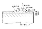
従来、半導体チップを実装基板に実装する方法としては、図11又は図12に示すような半導体チップを用いてフェースダウンボンディングを行なうものが知られている。
【0003】
図11に示す半導体チップ1は、一方の主面にシリコンオキサイド等の絶縁膜2が形成されている。絶縁膜2の上には、WSi(タングステンシリサイド)層3a及びAl(アルミニウム)層3bを含む導出電極3を形成すると共に導出電極3を覆ってシリコンナイトライド等の絶縁膜4及びシリコンオキサイド等の絶縁膜5を順次に形成する。絶縁膜4,5の積層に導出電極3の一部に対応して接続孔Pを形成した後、接続孔P内にはAuワイヤボンダを用いて2段構造のAu(金)バンプ6を形成する。
【0004】
実装に際しては、半導体チップ1をAuバンプ6が下になるように裏返しにした後、Auバンプ6を実装基板(図示せず)の配線層に導電性接着剤で固着することによりフェースダウンボンディングを行なう。
【0005】
一方、図12に示す半導体チップ1は、図1の半導体チップ1と同様に絶縁膜2の上に導出電極3及び絶縁膜4,5を形成した構成になっている。絶縁膜4,5の積層に導出電極3の一部に対応して接続孔を形成した後、該接続孔及び絶縁膜5を覆ってTi(チタン)膜7a及びNi(ニッケル)膜7bを順次に形成してから膜7a,7bの積層をホトリソグラフィ及び選択エッチング処理によりパターニングして接続孔内及びその周辺部に残存する膜7a,7bからなるバリア層7を形成する。この後、例えばレジストをマスクとする選択的Auめっき処理により面積20μm×20μm、高さ20μm程度のAuバンプ8を接続孔から突出するようにバリア層7上に形成する。
【0006】
実装に際しては、半導体チップ1をAuバンプ8が下になるように裏返しにした後、Auバンプ8を実装基板(図示せず)の配線層に半田又は導電性接着剤により固着することによりフェースダウンボンディングを行なう。
【0007】
【発明が解決しようとする課題】
図11に関して前述した方法によると、ワイヤボンダを用いて2段構造のAuバンプ6を形成するので、導出電極3としては、少なくとも70μm×70μm程度の面積が必要であり、導出電極サイズ乃至チップサイズの縮小が制限される不都合があった。
【0008】
また、図12に関して前述した方法によると、Auバンプ8としてかなり小さなものを形成できるが、工程が煩雑であると共に高価なAuめっき浴を必要とするため、コスト高となる不都合があった。
【0009】
この発明の目的は、低コストで導出電極サイズ乃至チップサイズの縮小を可能にする新規な半導体チップの実装方法及び実装構造を提供することにある。
【0010】
【課題を解決するための手段】
この発明に係る第1の半導体チップの実装構造は、
一方の主面に導出電極が形成された半導体チップと、
レーザー光透過性の導電層を最下層とする積層からなるか又はレーザー光透過性の導電層からなる配線層が一方の主面に形成されると共に少なくとも前記配線層の被接続部に対応する一部がレーザー光透過性を有する実装基板であって前記一方の主面には前記配線層を覆って絶縁膜が形成されると共に該絶縁膜には前記配線層の被接続部に対応した接続孔が設けられ、前記接続孔内で前記配線層の上には半田層が設けられたものと
を備え、前記実装基板側からのレーザーボンディングにより前記半導体チップの導出電極を前記半田層を介して前記配線層の被接続部に接続したものである。
【0011】
この発明に係る第1の半導体チップの実装構造によれば、半導体チップの導出電極と実装基板の配線層とをレーザーボンディングにより接続するようにしたので、接続面積の低減が可能となる。すなわち、レーザー光は、直径1〜25μm程度まで絞れるので、接続面積を25μm×25μm以下に小さくすることができ、ひいては導出電極サイズ乃至チップサイズを小さくすることができる。また、レーザーボンディングは、図12の方法に比べて工程や設備が簡単であり、低コストで済む。
【0013】
この発明に係る半導体チップの実装方法は、
一方の主面に導出電極が形成された半導体チップを準備する工程と、
一方の主面に配線層が形成されると共に該配線層を覆って絶縁膜が形成された実装基板であって少なくとも前記配線層の被接続部に対応する一部がレーザー光透過性を有するものを準備する工程と、
前記半導体チップの導出電極を前記配線層の被接続部の上で前記絶縁膜に接触させた状態で前記実装基板の一部を介して前記被接続部にレーザー光を照射することにより前記絶縁膜を破って前記導出電極を前記被接続部に接続する工程と
を含むものである。また、この発明に係る第2の半導体チップの実装構造は、
一方の主面に導出電極が形成された半導体チップと、
一方の主面に配線層が形成されると共に該配線層を覆って絶縁膜が形成された実装基板であって少なくとも前記配線層の被接続部に対応する一部がレーザー光透過性を有するものと
を備え、前記実装基板側からのレーザーボンディングにより前記絶縁膜を破って前記半導体チップの導出電極を前記配線層の被接続部に接続したものである。この発明に係る半導体チップの実装方法及び第2の半導体チップの実装構造によれば、実装基板上に配線層を覆って絶縁膜を形成し、レーザーボンディングにより該絶縁膜を破って導出電極と配線層とを接続するようにしたので、絶縁膜に接続孔を設ける工程が不要となり、工程が一層簡単となる。
【0014】
【発明の実施の形態】
図1〜3は、この発明の一実施形態に係る半導体チップの実装方法を示すもので、各々の図に対応する工程(1)〜(3)を順次に説明する。
【0015】
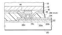
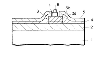
(1)例えばシリコンからなり且つ所望のICを内蔵した半導体チップ10を準備する。半導体チップ10の一方の主面には、シリコンオキサイド等の絶縁膜12が形成されている。絶縁膜12の上には、WSi層14aにAl層14bを重ねた構成の導出電極14を形成する。WSi層14aの代りにMoSi(モリブデンシリサイド)層等を用いたり、Al層14bの代りにAl合金(例えばAl−Si−Cu)層等を用いたりしてもよい。導出電極14は、方形状の半導体チップ10の四辺に沿って多数個形成されるものであるが、図1では便宜上1つのみ示した。
【0016】
絶縁膜12の上には、導出電極14を覆って絶縁膜16,18をCVD(ケミカル・ベーパー・デポジション)法等により形成する。一例として、絶縁膜16は、1000nmの厚さのシリコンナイトライド膜とし、絶縁膜18は、150nmの厚さのシリコンオキサイド膜とすることができる。
【0017】
絶縁膜16,18の積層には、ホトリソグラフィ及び選択的エッチング処理により導出電極14の一部に対応した接続孔Qを形成する。そして、絶縁膜18の上に接続孔Qを覆ってスパッタ法等によりNi層を被着し、該Ni層をホトリソグラフィ及び選択的エッチング処理によりパターニングして接続孔Q内及び接続孔Qの周辺部を覆うNi層14cを形成する。Ni層14cは、実装基板の配線層に接続される接続層として用いられるもので、一例として100nmの厚さに形成することができる。
(2)半導体チップ10を準備する前又は後、あるいは半導体チップ10を準備するのに並行して実装基板20を準備する。実装基板20は、一例としてレーザー光透過性を有するガラス基板からなるもので、この基板を構成するガラス材料としてはシリコンと熱膨張係数が近似したもの(例えば30〜300℃において25×10-7〜40×10-7/℃程度の熱膨張係数を有するもの)を用いるのが好ましい。
【0018】
実装基板20の一方の主面には、ITO(イットリウム・ティン・オキサイド)層22aにCu(銅)層22bを重ねた構成の配線層22を形成する。ITO層22aは、レーザー光に対して透明な導電層であり、例えば1〜20μmの厚さに形成される。Cu層22bは、例えば1〜5μmの厚さに形成される。配線層22は、半導体チップ10に設けた14等の多数の導出電極に対応して多数個形成されるものであるが、図2では便宜上1つのみ示した。なお、配線層22は、Cu層22bを省略してITO層22aのみとしたり、ITO層22aの代りにNi層を用いてNi層にCu層22bを重ねた構成としたりすることもできる。
【0019】
実装基板20の一方の主面には、配線層22を覆ってポリイミド樹脂等の絶縁膜24を形成する。絶縁膜24は、例えば1〜3μmの厚さに形成することができる。絶縁膜24に所望の接続孔を形成した後、該接続孔内に1〜5μmの厚さの半田層22cを形成する。
【0020】
次に、図1の半導体チップ10を裏返しにして配線層22に対する位置合せを行ない、導出電極14のNi層14cを配線層22上の半田層22cに接触させる。そして、このような接触状態において実装基板20の他方の主面側から直径1〜25μmに絞ったレーザー光Lを焦点がCu層22b及び半田層22cに合うように照射してNi層14cと半田層22cとを結合させる。この結果、導出電極14が配線層22と電気的に接続される。
【0021】
このようなレーザーボンディングは、半導体チップ10上の多数の導出電極について1つずつ順次に行なう。他の方法としては、複数のレーザー発光部を設け、複数の導出電極について同時にレーザーボンディングを行なうようにしてもよい。なお、実装基板20は、少なくとも配線層22の被接続部に対応する一部がレーザー光透過性を有していればよい。
(3)レーザーボンディングの終了後、半導体チップ10と実装基板20との間の間隙には絶縁性の樹脂を充填して樹脂層28を形成する。樹脂層28は、半導体チップ10と実装基板20との熱膨張係数の差による歪を吸収するように作用するので、半導体チップ10の実装基板20に対する取付強度を増大させるのに役立つ。
【0022】
図4,5は、ボンディング工程の他の例を示すもので、図2と同様の部分には同様の符号を付して詳細な説明を省略する。
【0023】
図4の例では、半導体チップ10の導出電極14の頂部にNi層14cの凹部Q’から突出するように半田バンプ26を設ける。そして、半導体チップ10を裏返しにして位置合せを行ない、半田バンプ26を配線層22のCu層22bに接触させた状態で半田バンプ26に実装基板20の他方の主面側からレーザー光Lを照射して半田バンプ26とCu層22bとを結合させる。この結果、導出電極14が配線層22に電気的に接続される。
【0024】
図4の方法によると、半導体チップ10に接続不良が生じた場合、その半導体チップを取外して他の同種の半導体チップをレーザーボンディングにより簡単に接続することができる。
【0025】
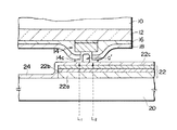
図5の例では、半田層22cをITO層22a及びCu層22bと同じ配線パターンに従って形成した後、実装基板20の一方の主面に層22a〜22cを含む配線層22を覆って絶縁膜24を形成する。半田層22cは、Cu層22bの一部に対応して形成し、それを覆って絶縁膜24を形成してもよい。いずれにしても、絶縁膜24には接続孔を設けない。
【0026】
次に、半導体チップ10を裏返しにして位置合せを行ない、導出電極14のNi層14cを絶縁膜24に接触させた状態で実装基板20の他方の主面側からレーザー光L1 又はL2 を照射し、絶縁膜24を破ってNi層14cと半田層22cとを結合させる。この結果、導出電極14が配線層22に電気的に接続される。
【0027】
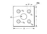
図5の方法によれば、絶縁膜24に接続孔を設けなくてよいので、工程が簡単となる。また、レーザー光L1 ,L2 を用いて複数個所をボンディングすると、電気的接続の信頼性が向上する。一例として、図6に示すように導出電極14のNi層14cにおいて凹部Q’の周辺でS1 〜S4 の4個所をボンディングすることができる。この場合、Ni層14cが平面的に見て正方形であるとすると、二辺の長さA,Bをいずれも25μmとしても、L1 ,L2 等のレーザー光の直径Rを4μmに絞ることでS1 〜S4 の4個所でボンディングを行なうことができる。S1 〜S4 の4個所のうち例えば1個所でボンディング不良が発生しても、他の3個所で電気的接続を確保することができる。
【0028】
【実施例】
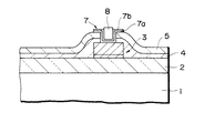
図7は、ボンディングの第1の実施例を示すもので、図2と同様の部分には同様の符号を付して詳細な説明を省略する。
【0029】
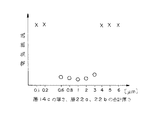
実装基板20の一方の主面には、ITO層22a及びCu層22bを含む配線層22を形成すると共に配線層22を覆ってポリイミド樹脂からなる絶縁膜24を形成した。ITO層22a及びCu層22bの合計厚さを図8の横軸に示すような種々の値とし、各値毎に実装基板のサンプルを作成した。
【0030】
一方、半導体チップとしては、図1に示すように一方の主面が絶縁膜12で覆われると共に絶縁膜12の上にWSi層14a、Al層14b及びNi層14cの積層からなる導出電極14を設けたものを作成した。Ni層14cの厚さを図8の横軸に示すような種々の値とし、各値毎に半導体チップのサンプルを作成した。
【0031】
実装基板20と半導体チップについて図8の厚さで対応するサンプル毎に図7に示すようにNi層14cを絶縁膜24に接触させた状態で実装基板20の他方の主面側からレーザー光Lを照射し、絶縁膜24を破ってのNi層14cとCu層22bとの結合を試みた。レーザーとしては、波長1064nmのYAG(イットリウム・アルミニウム・ガーネット)レーザーを用い、出力エネルギーを9mJ/pulseとし、パルス幅を10nsecとした。レーザー出力は、フィルタを用いて75%に抑えた。
【0032】
図8は、レーザーボンディングの終了後にボンディングに係る組合せサンプル毎に導出電極−配線層間の電気抵抗を測定した結果を示すものである。○印を付したサンプルは、電気抵抗が低く、良好な接続状態が得られたものであり、×印を付したサンプルは、電気抵抗が高く、接続状態が不良のものである。図8によれば、Ni層14cの厚さを0.6〜3μmとし、ITO層22a及びCu層22bの合計厚さを0.6〜3μmとしたときに良好な接続状態が得られることがわかる。
【0033】
図9は、ボンディングの第2の実施例を示すもので、図2と同様の部分には同様の符号を付して詳細な説明を省略する。
【0034】
実装基板20の一方の主面には、ITO層22a及び半田層22cを含む配線層22を形成すると共に配線層22を覆ってポリイミド樹脂からなる絶縁膜24を形成した。半田層22cを構成する半田としては、組成がIn−20Sn−0.8Agのものを用いた。ITO層22a及び半田層22cの合計厚さを図10の横軸に示すような種々の値とし、各値毎に実装基板のサンプルを作成した。また、図7に関して前述したと同様にしてAl層14b,Ni層14c等を有する半導体チップのサンプルを図10の横軸に示す各値毎に作成した。
【0035】
実装基板20と半導体チップについて図10の厚さで対応するサンプル毎に図9に示すようにNi層14cを絶縁膜24に接触させた状態で実装基板20の他方の主面側からレーザー光Lを照射し、絶縁膜24を破ってのNi層14cと半田層22cとの結合を試みた。レーザーとしては、波長1064nmのYAGレーザーを用い、出力エネルギーを6mJ/pulseとし、パルス幅を10nsecとした。レーザー出力は、フィルタを用いて75%に抑えた。
【0036】
図10は、レーザーボンディングの終了後にボンディングに係る組合せサンプル毎に導出電極−配線層間の電気抵抗を測定した結果を図8と同様にして示したものである。図10によれば、図8の場合と類似した結果が得られることがわかる。
【0037】
【発明の効果】
以上のように、この発明によれば、半導体チップの導出電極と実装基板の配線層とをレーザーボンディングで接続するようにしたので、接続面積の低減が可能となり、ひいては導出電極サイズ乃至チップサイズの縮小が可能となる効果が得られるものである。
【0038】
また、半田を用いる従来技術では、半田にPb(鉛)を入れないと信頼性の高い電気接続が得られなかったが、この発明ではレーザーボンディングにより接続を行なうようにしたので、Pbなしの半田でも接続可能であり、Pb不使用とすれば環境問題を引き起こすおそれもない。また、Pbなしの半田を用いる従来技術では、N2 (窒素)雰囲気中でないと接続できなかったが、この発明ではN2 雰囲気中でなくても良好な接続を得ることができ、高価な雰囲気調整設備も不要である。
【0039】
さらに、図12の方法に比べて工程や設備が簡単であり、コスト低減が可能になる利点もある。
【図面の簡単な説明】
【図1】 この発明の一実施形態に係る半導体チップの実装方法における半導体チップ準備工程を示す断面図である。
【図2】 図1の工程に続くボンディング工程を示す断面図である。
【図3】 図2の工程に続く樹脂充填工程を示す断面図である。
【図4】 ボンディング工程の他の例を示す断面図である。
【図5】 ボンディング工程の更に他の例を示す断面図である。
【図6】 図5の工程におけるNi層のボンディング個所を示す平面図である。
【図7】 ボンディングの第1の実施例を示す断面図である。
【図8】 第1の実施例において層14c,22a,22bの厚さを変化させてボンディングした場合の電気抵抗の測定結果を示すグラフである。
【図9】 ボンディングの第2の実施例を示す断面図である。
【図10】 第2の実施例において層14c,22a,22cの厚さを変化させてボンディングした場合の電気抵抗の測定結果を示すグラフである。
【図11】 従来のボンディング工程で用いられる半導体チップの一例を示す断面図である。
【図12】 従来のボンディング工程で用いられる半導体チップの他の例を示す断面図である。
【符号の説明】
10:半導体チップ、12,16,18,24:絶縁膜、14:導出電極、14a:WSi層、14b:Al層、14c:Ni層、20:実装基板、22:配線層、22a:ITO層、22b:Cu層、22c:半田層、26:半田バンプ、28:樹脂層、L,L1 ,L2 :レーザー光。
Claims (3)
- 一方の主面に導出電極が形成された半導体チップと、
レーザー光透過性の導電層を最下層とする積層からなるか又はレーザー光透過性の導電層からなる配線層が一方の主面に形成されると共に少なくとも前記配線層の被接続部に対応する一部がレーザー光透過性を有する実装基板であって前記一方の主面には前記配線層を覆って絶縁膜が形成されると共に該絶縁膜には前記配線層の被接続部に対応した接続孔が設けられ、前記接続孔内で前記配線層の上には半田層が設けられたものと
を備え、前記実装基板側からのレーザーボンディングにより前記半導体チップの導出電極を前記半田層を介して前記配線層の被接続部に接続した半導体チップの実装構造。 - 一方の主面に導出電極が形成された半導体チップを準備する工程と、
一方の主面に配線層が形成されると共に該配線層を覆って絶縁膜が形成された実装基板であって少なくとも前記配線層の被接続部に対応する一部がレーザー光透過性を有するものを準備する工程と、
前記半導体チップの導出電極を前記配線層の被接続部の上で前記絶縁膜に接触させた状態で前記実装基板の一部を介して前記被接続部にレーザー光を照射することにより前記絶縁膜を破って前記導出電極を前記被接続部に接続する工程と
を含む半導体チップの実装方法。 - 一方の主面に導出電極が形成された半導体チップと、
一方の主面に配線層が形成されると共に該配線層を覆って絶縁膜が形成された実装基板であって少なくとも前記配線層の被接続部に対応する一部がレーザー光透過性を有するものと
を備え、前記実装基板側からのレーザーボンディングにより前記絶縁膜を破って前記半導体チップの導出電極を前記配線層の被接続部に接続した半導体チップの実装構造。
Priority Applications (2)
| Application Number | Priority Date | Filing Date | Title |
|---|---|---|---|
| JP29774496A JP3663786B2 (ja) | 1996-10-14 | 1996-10-21 | 半導体チップの実装方法と実装構造 |
| US08/949,702 US5946597A (en) | 1996-10-14 | 1997-10-14 | Semiconductor chip mounting method |
Applications Claiming Priority (3)
| Application Number | Priority Date | Filing Date | Title |
|---|---|---|---|
| JP8-291164 | 1996-10-14 | ||
| JP29116496 | 1996-10-14 | ||
| JP29774496A JP3663786B2 (ja) | 1996-10-14 | 1996-10-21 | 半導体チップの実装方法と実装構造 |
Related Child Applications (1)
| Application Number | Title | Priority Date | Filing Date |
|---|---|---|---|
| JP2004302516A Division JP4059240B2 (ja) | 1996-10-14 | 2004-10-18 | 半導体チップの実装構造 |
Publications (2)
| Publication Number | Publication Date |
|---|---|
| JPH10178046A JPH10178046A (ja) | 1998-06-30 |
| JP3663786B2 true JP3663786B2 (ja) | 2005-06-22 |
Family
ID=26558424
Family Applications (1)
| Application Number | Title | Priority Date | Filing Date |
|---|---|---|---|
| JP29774496A Expired - Fee Related JP3663786B2 (ja) | 1996-10-14 | 1996-10-21 | 半導体チップの実装方法と実装構造 |
Country Status (2)
| Country | Link |
|---|---|
| US (1) | US5946597A (ja) |
| JP (1) | JP3663786B2 (ja) |
Families Citing this family (14)
| Publication number | Priority date | Publication date | Assignee | Title |
|---|---|---|---|---|
| TW373197B (en) * | 1997-05-14 | 1999-11-01 | Murata Manufacturing Co | Electronic device having electric wires and the manufacturing method thereof |
| DE59812923D1 (de) * | 1997-07-23 | 2005-08-18 | Infineon Technologies Ag | Vorrichtung und verfahren zur herstellung einer chip-substrat-verbindung |
| KR100254323B1 (ko) * | 1997-08-01 | 2000-05-01 | 윤종용 | 집적회로 납땜 장치 및 방법 |
| US6119924A (en) * | 1998-05-12 | 2000-09-19 | Murata Manufacturing Co., Ltd. | Electronic device having electric wires and method of producing same |
| EP0964608A3 (en) * | 1998-06-12 | 2001-09-05 | Ford Motor Company | Method for laser soldering |
| JP2002050716A (ja) * | 2000-08-02 | 2002-02-15 | Dainippon Printing Co Ltd | 半導体装置及びその作製方法 |
| GB0123676D0 (en) * | 2001-10-02 | 2001-11-21 | Poly Flex Circuits Ltd | Method of manufacturing circuits |
| US20030224581A1 (en) * | 2002-06-03 | 2003-12-04 | Robert Bosch Gmbh | Flip chip packaging process using laser-induced metal bonding technology, system utilizing the method, and device created by the method |
| JP2004273895A (ja) * | 2003-03-11 | 2004-09-30 | Disco Abrasive Syst Ltd | 半導体ウエーハの分割方法 |
| EP1641035A1 (en) * | 2004-09-27 | 2006-03-29 | STMicroelectronics S.r.l. | Mounting method of electronic power components on printed circuit boards |
| JP2007222907A (ja) * | 2006-02-23 | 2007-09-06 | Denso Corp | 配線部材のレーザー照射式半田接合方法 |
| FR2913145B1 (fr) * | 2007-02-22 | 2009-05-15 | Stmicroelectronics Crolles Sas | Assemblage de deux parties de circuit electronique integre |
| WO2011004469A1 (ja) * | 2009-07-08 | 2011-01-13 | トヨタ自動車株式会社 | 半導体装置とその製造方法 |
| JP5939184B2 (ja) * | 2013-03-22 | 2016-06-22 | ソニー株式会社 | 半導体装置の製造方法 |
Family Cites Families (2)
| Publication number | Priority date | Publication date | Assignee | Title |
|---|---|---|---|---|
| JPH0429338A (ja) * | 1990-05-24 | 1992-01-31 | Nippon Mektron Ltd | Icの搭載用回路基板及びその搭載方法 |
| JP2813507B2 (ja) * | 1992-04-23 | 1998-10-22 | 三菱電機株式会社 | ボンディング方法およびボンディング装置 |
-
1996
- 1996-10-21 JP JP29774496A patent/JP3663786B2/ja not_active Expired - Fee Related
-
1997
- 1997-10-14 US US08/949,702 patent/US5946597A/en not_active Expired - Fee Related
Also Published As
| Publication number | Publication date |
|---|---|
| JPH10178046A (ja) | 1998-06-30 |
| US5946597A (en) | 1999-08-31 |
Similar Documents
| Publication | Publication Date | Title |
|---|---|---|
| US5104820A (en) | Method of fabricating electronic circuitry unit containing stacked IC layers having lead rerouting | |
| JP3663786B2 (ja) | 半導体チップの実装方法と実装構造 | |
| US5925931A (en) | Semiconductor device having interconnect lines and connection electrodes formed in groove portions of an insulating layer | |
| JP2966972B2 (ja) | 半導体チップキャリアとそれを実装したモジュール及びそれを組み込んだ電子機器 | |
| US6784543B2 (en) | External connection terminal and semiconductor device | |
| KR100290193B1 (ko) | 반도체장치및그제조방법 | |
| JP4685834B2 (ja) | 集積回路デバイス | |
| US10128129B2 (en) | Method of manufacturing semiconductor device | |
| JPS6355213B2 (ja) | ||
| JP3506393B2 (ja) | 液晶表示装置とその製造方法、プリンタとその製造方法 | |
| CN1983612A (zh) | 半导体装置及其制造方法 | |
| US7230326B2 (en) | Semiconductor device and wire bonding chip size package therefor | |
| US20080142945A1 (en) | Semiconductor package with redistribution layer of semiconductor chip directly contacted with substrate and method of fabricating the same | |
| JP3502056B2 (ja) | 半導体装置およびこれを用いた積層構造体 | |
| EP0511218B1 (en) | Fabricating eletronic circuitry unit containing stacked ic layers having lead rerouting | |
| JP4046568B2 (ja) | 半導体装置、積層型半導体装置およびそれらの製造方法 | |
| JP4059240B2 (ja) | 半導体チップの実装構造 | |
| JP2725611B2 (ja) | 半導体装置 | |
| JPH08124930A (ja) | 半導体装置 | |
| JP3458056B2 (ja) | 半導体装置およびその実装体 | |
| US20100330744A1 (en) | Ultrathin semiconductor circuit having contact bumps and corresponding production method | |
| JPH1027824A (ja) | 突起電極を有する半導体装置及びその製造方法 | |
| JP2001118957A (ja) | 半導体装置 | |
| JPH02168640A (ja) | 異なる基板間の接続構造 | |
| US6204164B1 (en) | Method of making electrical connections to integrated circuit |
Legal Events
| Date | Code | Title | Description |
|---|---|---|---|
| A131 | Notification of reasons for refusal |
Free format text: JAPANESE INTERMEDIATE CODE: A131 Effective date: 20040824 |
|
| A521 | Request for written amendment filed |
Free format text: JAPANESE INTERMEDIATE CODE: A523 Effective date: 20041018 |
|
| TRDD | Decision of grant or rejection written | ||
| A01 | Written decision to grant a patent or to grant a registration (utility model) |
Free format text: JAPANESE INTERMEDIATE CODE: A01 Effective date: 20050308 |
|
| A61 | First payment of annual fees (during grant procedure) |
Free format text: JAPANESE INTERMEDIATE CODE: A61 Effective date: 20050321 |
|
| R150 | Certificate of patent or registration of utility model |
Free format text: JAPANESE INTERMEDIATE CODE: R150 |
|
| S531 | Written request for registration of change of domicile |
Free format text: JAPANESE INTERMEDIATE CODE: R313532 |
|
| R350 | Written notification of registration of transfer |
Free format text: JAPANESE INTERMEDIATE CODE: R350 |
|
| FPAY | Renewal fee payment (event date is renewal date of database) |
Free format text: PAYMENT UNTIL: 20090408 Year of fee payment: 4 |
|
| FPAY | Renewal fee payment (event date is renewal date of database) |
Free format text: PAYMENT UNTIL: 20090408 Year of fee payment: 4 |
|
| FPAY | Renewal fee payment (event date is renewal date of database) |
Free format text: PAYMENT UNTIL: 20100408 Year of fee payment: 5 |
|
| LAPS | Cancellation because of no payment of annual fees |