JP3556679B2 - Electro-optical device - Google Patents
Electro-optical device Download PDFInfo
- Publication number
- JP3556679B2 JP3556679B2 JP16430292A JP16430292A JP3556679B2 JP 3556679 B2 JP3556679 B2 JP 3556679B2 JP 16430292 A JP16430292 A JP 16430292A JP 16430292 A JP16430292 A JP 16430292A JP 3556679 B2 JP3556679 B2 JP 3556679B2
- Authority
- JP
- Japan
- Prior art keywords
- electro
- region
- channel
- optical device
- film
- Prior art date
- Legal status (The legal status is an assumption and is not a legal conclusion. Google has not performed a legal analysis and makes no representation as to the accuracy of the status listed.)
- Expired - Fee Related
Links
- 239000010408 film Substances 0.000 claims description 76
- 239000000758 substrate Substances 0.000 claims description 45
- 239000004065 semiconductor Substances 0.000 claims description 41
- 239000012535 impurity Substances 0.000 claims description 25
- 239000010409 thin film Substances 0.000 claims description 10
- 230000015572 biosynthetic process Effects 0.000 claims description 8
- 229910021419 crystalline silicon Inorganic materials 0.000 claims description 5
- IJGRMHOSHXDMSA-UHFFFAOYSA-N Atomic nitrogen Chemical compound N#N IJGRMHOSHXDMSA-UHFFFAOYSA-N 0.000 claims description 4
- QVGXLLKOCUKJST-UHFFFAOYSA-N atomic oxygen Chemical compound [O] QVGXLLKOCUKJST-UHFFFAOYSA-N 0.000 claims description 4
- 239000001301 oxygen Substances 0.000 claims description 4
- 229910052760 oxygen Inorganic materials 0.000 claims description 4
- OKTJSMMVPCPJKN-UHFFFAOYSA-N Carbon Chemical compound [C] OKTJSMMVPCPJKN-UHFFFAOYSA-N 0.000 claims description 2
- 229910052799 carbon Inorganic materials 0.000 claims description 2
- 229910052757 nitrogen Inorganic materials 0.000 claims description 2
- 239000010407 anodic oxide Substances 0.000 claims 1
- 238000000034 method Methods 0.000 description 58
- 239000010410 layer Substances 0.000 description 47
- 230000008569 process Effects 0.000 description 27
- 239000013078 crystal Substances 0.000 description 19
- VYPSYNLAJGMNEJ-UHFFFAOYSA-N silicon dioxide Inorganic materials O=[Si]=O VYPSYNLAJGMNEJ-UHFFFAOYSA-N 0.000 description 19
- XUIMIQQOPSSXEZ-UHFFFAOYSA-N Silicon Chemical compound [Si] XUIMIQQOPSSXEZ-UHFFFAOYSA-N 0.000 description 18
- 229910052710 silicon Inorganic materials 0.000 description 18
- 239000010703 silicon Substances 0.000 description 18
- 239000011159 matrix material Substances 0.000 description 17
- 229910021417 amorphous silicon Inorganic materials 0.000 description 16
- 229910052814 silicon oxide Inorganic materials 0.000 description 16
- 150000002500 ions Chemical class 0.000 description 12
- 239000004973 liquid crystal related substance Substances 0.000 description 11
- 238000005468 ion implantation Methods 0.000 description 9
- 238000004519 manufacturing process Methods 0.000 description 9
- 239000000463 material Substances 0.000 description 9
- 239000003990 capacitor Substances 0.000 description 7
- 230000005684 electric field Effects 0.000 description 7
- 238000004518 low pressure chemical vapour deposition Methods 0.000 description 6
- 229910021420 polycrystalline silicon Inorganic materials 0.000 description 6
- 239000012212 insulator Substances 0.000 description 5
- 238000005224 laser annealing Methods 0.000 description 5
- 229910021421 monocrystalline silicon Inorganic materials 0.000 description 5
- 238000004544 sputter deposition Methods 0.000 description 5
- 229910052581 Si3N4 Inorganic materials 0.000 description 4
- 239000002585 base Substances 0.000 description 4
- 230000008901 benefit Effects 0.000 description 4
- 238000010586 diagram Methods 0.000 description 4
- 230000000694 effects Effects 0.000 description 4
- 238000005516 engineering process Methods 0.000 description 4
- 239000011521 glass Substances 0.000 description 4
- 238000002513 implantation Methods 0.000 description 4
- 230000003647 oxidation Effects 0.000 description 4
- 238000007254 oxidation reaction Methods 0.000 description 4
- 230000002093 peripheral effect Effects 0.000 description 4
- 238000005268 plasma chemical vapour deposition Methods 0.000 description 4
- HQVNEWCFYHHQES-UHFFFAOYSA-N silicon nitride Chemical compound N12[Si]34N5[Si]62N3[Si]51N64 HQVNEWCFYHHQES-UHFFFAOYSA-N 0.000 description 4
- 230000001133 acceleration Effects 0.000 description 3
- 239000003513 alkali Substances 0.000 description 3
- 229910052782 aluminium Inorganic materials 0.000 description 3
- XAGFODPZIPBFFR-UHFFFAOYSA-N aluminium Chemical compound [Al] XAGFODPZIPBFFR-UHFFFAOYSA-N 0.000 description 3
- -1 boron fluoride ions Chemical class 0.000 description 3
- 230000008859 change Effects 0.000 description 3
- 238000002425 crystallisation Methods 0.000 description 3
- 230000008025 crystallization Effects 0.000 description 3
- 239000011229 interlayer Substances 0.000 description 3
- 230000003071 parasitic effect Effects 0.000 description 3
- 229910052698 phosphorus Inorganic materials 0.000 description 3
- 239000011574 phosphorus Substances 0.000 description 3
- 239000010453 quartz Substances 0.000 description 3
- 238000003860 storage Methods 0.000 description 3
- ZOXJGFHDIHLPTG-UHFFFAOYSA-N Boron Chemical compound [B] ZOXJGFHDIHLPTG-UHFFFAOYSA-N 0.000 description 2
- DGAQECJNVWCQMB-PUAWFVPOSA-M Ilexoside XXIX Chemical compound C[C@@H]1CC[C@@]2(CC[C@@]3(C(=CC[C@H]4[C@]3(CC[C@@H]5[C@@]4(CC[C@@H](C5(C)C)OS(=O)(=O)[O-])C)C)[C@@H]2[C@]1(C)O)C)C(=O)O[C@H]6[C@@H]([C@H]([C@@H]([C@H](O6)CO)O)O)O.[Na+] DGAQECJNVWCQMB-PUAWFVPOSA-M 0.000 description 2
- NBIIXXVUZAFLBC-UHFFFAOYSA-N Phosphoric acid Chemical compound OP(O)(O)=O NBIIXXVUZAFLBC-UHFFFAOYSA-N 0.000 description 2
- OAICVXFJPJFONN-UHFFFAOYSA-N Phosphorus Chemical compound [P] OAICVXFJPJFONN-UHFFFAOYSA-N 0.000 description 2
- BOTDANWDWHJENH-UHFFFAOYSA-N Tetraethyl orthosilicate Chemical compound CCO[Si](OCC)(OCC)OCC BOTDANWDWHJENH-UHFFFAOYSA-N 0.000 description 2
- 238000000137 annealing Methods 0.000 description 2
- 230000005540 biological transmission Effects 0.000 description 2
- 229910052796 boron Inorganic materials 0.000 description 2
- 238000000151 deposition Methods 0.000 description 2
- 230000008021 deposition Effects 0.000 description 2
- 238000005530 etching Methods 0.000 description 2
- 239000007943 implant Substances 0.000 description 2
- TWNQGVIAIRXVLR-UHFFFAOYSA-N oxo(oxoalumanyloxy)alumane Chemical compound O=[Al]O[Al]=O TWNQGVIAIRXVLR-UHFFFAOYSA-N 0.000 description 2
- 239000002994 raw material Substances 0.000 description 2
- 238000001004 secondary ion mass spectrometry Methods 0.000 description 2
- 238000000926 separation method Methods 0.000 description 2
- 239000002210 silicon-based material Substances 0.000 description 2
- 229910052708 sodium Inorganic materials 0.000 description 2
- 239000011734 sodium Substances 0.000 description 2
- 239000000243 solution Substances 0.000 description 2
- 229910015900 BF3 Inorganic materials 0.000 description 1
- GRYLNZFGIOXLOG-UHFFFAOYSA-N Nitric acid Chemical compound O[N+]([O-])=O GRYLNZFGIOXLOG-UHFFFAOYSA-N 0.000 description 1
- BLRPTPMANUNPDV-UHFFFAOYSA-N Silane Chemical compound [SiH4] BLRPTPMANUNPDV-UHFFFAOYSA-N 0.000 description 1
- 239000002253 acid Substances 0.000 description 1
- 230000004913 activation Effects 0.000 description 1
- 230000002411 adverse Effects 0.000 description 1
- 229910000147 aluminium phosphate Inorganic materials 0.000 description 1
- 238000005229 chemical vapour deposition Methods 0.000 description 1
- 230000000295 complement effect Effects 0.000 description 1
- 230000008878 coupling Effects 0.000 description 1
- 238000010168 coupling process Methods 0.000 description 1
- 238000005859 coupling reaction Methods 0.000 description 1
- 230000007547 defect Effects 0.000 description 1
- 238000009792 diffusion process Methods 0.000 description 1
- PZPGRFITIJYNEJ-UHFFFAOYSA-N disilane Chemical compound [SiH3][SiH3] PZPGRFITIJYNEJ-UHFFFAOYSA-N 0.000 description 1
- 239000002019 doping agent Substances 0.000 description 1
- 230000009977 dual effect Effects 0.000 description 1
- 230000001747 exhibiting effect Effects 0.000 description 1
- 230000005669 field effect Effects 0.000 description 1
- 238000007667 floating Methods 0.000 description 1
- 230000006870 function Effects 0.000 description 1
- 239000007789 gas Substances 0.000 description 1
- 238000010438 heat treatment Methods 0.000 description 1
- 239000001257 hydrogen Substances 0.000 description 1
- 229910052739 hydrogen Inorganic materials 0.000 description 1
- 238000002347 injection Methods 0.000 description 1
- 239000007924 injection Substances 0.000 description 1
- 230000009545 invasion Effects 0.000 description 1
- 230000014759 maintenance of location Effects 0.000 description 1
- 229910052751 metal Inorganic materials 0.000 description 1
- 239000002184 metal Substances 0.000 description 1
- 229910017604 nitric acid Inorganic materials 0.000 description 1
- 230000001590 oxidative effect Effects 0.000 description 1
- 238000002161 passivation Methods 0.000 description 1
- 230000035515 penetration Effects 0.000 description 1
- 238000000206 photolithography Methods 0.000 description 1
- 229920002120 photoresistant polymer Polymers 0.000 description 1
- 229920005591 polysilicon Polymers 0.000 description 1
- 238000001556 precipitation Methods 0.000 description 1
- 238000002310 reflectometry Methods 0.000 description 1
- 239000007787 solid Substances 0.000 description 1
- 230000003068 static effect Effects 0.000 description 1
- 238000002834 transmittance Methods 0.000 description 1
Images


Classifications
-
- H—ELECTRICITY
- H01—ELECTRIC ELEMENTS
- H01L—SEMICONDUCTOR DEVICES NOT COVERED BY CLASS H10
- H01L27/00—Devices consisting of a plurality of semiconductor or other solid-state components formed in or on a common substrate
- H01L27/02—Devices consisting of a plurality of semiconductor or other solid-state components formed in or on a common substrate including semiconductor components specially adapted for rectifying, oscillating, amplifying or switching and having at least one potential-jump barrier or surface barrier; including integrated passive circuit elements with at least one potential-jump barrier or surface barrier
- H01L27/12—Devices consisting of a plurality of semiconductor or other solid-state components formed in or on a common substrate including semiconductor components specially adapted for rectifying, oscillating, amplifying or switching and having at least one potential-jump barrier or surface barrier; including integrated passive circuit elements with at least one potential-jump barrier or surface barrier the substrate being other than a semiconductor body, e.g. an insulating body
- H01L27/1214—Devices consisting of a plurality of semiconductor or other solid-state components formed in or on a common substrate including semiconductor components specially adapted for rectifying, oscillating, amplifying or switching and having at least one potential-jump barrier or surface barrier; including integrated passive circuit elements with at least one potential-jump barrier or surface barrier the substrate being other than a semiconductor body, e.g. an insulating body comprising a plurality of TFTs formed on a non-semiconducting substrate, e.g. driving circuits for AMLCDs
-
- H—ELECTRICITY
- H01—ELECTRIC ELEMENTS
- H01L—SEMICONDUCTOR DEVICES NOT COVERED BY CLASS H10
- H01L29/00—Semiconductor devices adapted for rectifying, amplifying, oscillating or switching, or capacitors or resistors with at least one potential-jump barrier or surface barrier, e.g. PN junction depletion layer or carrier concentration layer; Details of semiconductor bodies or of electrodes thereof ; Multistep manufacturing processes therefor
- H01L29/66—Types of semiconductor device ; Multistep manufacturing processes therefor
- H01L29/68—Types of semiconductor device ; Multistep manufacturing processes therefor controllable by only the electric current supplied, or only the electric potential applied, to an electrode which does not carry the current to be rectified, amplified or switched
- H01L29/76—Unipolar devices, e.g. field effect transistors
- H01L29/772—Field effect transistors
- H01L29/78—Field effect transistors with field effect produced by an insulated gate
- H01L29/786—Thin film transistors, i.e. transistors with a channel being at least partly a thin film
- H01L29/78603—Thin film transistors, i.e. transistors with a channel being at least partly a thin film characterised by the insulating substrate or support
-
- H—ELECTRICITY
- H01—ELECTRIC ELEMENTS
- H01L—SEMICONDUCTOR DEVICES NOT COVERED BY CLASS H10
- H01L29/00—Semiconductor devices adapted for rectifying, amplifying, oscillating or switching, or capacitors or resistors with at least one potential-jump barrier or surface barrier, e.g. PN junction depletion layer or carrier concentration layer; Details of semiconductor bodies or of electrodes thereof ; Multistep manufacturing processes therefor
- H01L29/66—Types of semiconductor device ; Multistep manufacturing processes therefor
- H01L29/68—Types of semiconductor device ; Multistep manufacturing processes therefor controllable by only the electric current supplied, or only the electric potential applied, to an electrode which does not carry the current to be rectified, amplified or switched
- H01L29/76—Unipolar devices, e.g. field effect transistors
- H01L29/772—Field effect transistors
- H01L29/78—Field effect transistors with field effect produced by an insulated gate
- H01L29/786—Thin film transistors, i.e. transistors with a channel being at least partly a thin film
- H01L29/78606—Thin film transistors, i.e. transistors with a channel being at least partly a thin film with supplementary region or layer in the thin film or in the insulated bulk substrate supporting it for controlling or increasing the safety of the device
- H01L29/78609—Thin film transistors, i.e. transistors with a channel being at least partly a thin film with supplementary region or layer in the thin film or in the insulated bulk substrate supporting it for controlling or increasing the safety of the device for preventing leakage current
-
- H—ELECTRICITY
- H01—ELECTRIC ELEMENTS
- H01L—SEMICONDUCTOR DEVICES NOT COVERED BY CLASS H10
- H01L29/00—Semiconductor devices adapted for rectifying, amplifying, oscillating or switching, or capacitors or resistors with at least one potential-jump barrier or surface barrier, e.g. PN junction depletion layer or carrier concentration layer; Details of semiconductor bodies or of electrodes thereof ; Multistep manufacturing processes therefor
- H01L29/66—Types of semiconductor device ; Multistep manufacturing processes therefor
- H01L29/68—Types of semiconductor device ; Multistep manufacturing processes therefor controllable by only the electric current supplied, or only the electric potential applied, to an electrode which does not carry the current to be rectified, amplified or switched
- H01L29/76—Unipolar devices, e.g. field effect transistors
- H01L29/772—Field effect transistors
- H01L29/78—Field effect transistors with field effect produced by an insulated gate
- H01L29/786—Thin film transistors, i.e. transistors with a channel being at least partly a thin film
- H01L29/78651—Silicon transistors
- H01L29/7866—Non-monocrystalline silicon transistors
- H01L29/78672—Polycrystalline or microcrystalline silicon transistor
- H01L29/78675—Polycrystalline or microcrystalline silicon transistor with normal-type structure, e.g. with top gate
-
- H—ELECTRICITY
- H01—ELECTRIC ELEMENTS
- H01L—SEMICONDUCTOR DEVICES NOT COVERED BY CLASS H10
- H01L29/00—Semiconductor devices adapted for rectifying, amplifying, oscillating or switching, or capacitors or resistors with at least one potential-jump barrier or surface barrier, e.g. PN junction depletion layer or carrier concentration layer; Details of semiconductor bodies or of electrodes thereof ; Multistep manufacturing processes therefor
- H01L29/66—Types of semiconductor device ; Multistep manufacturing processes therefor
- H01L29/68—Types of semiconductor device ; Multistep manufacturing processes therefor controllable by only the electric current supplied, or only the electric potential applied, to an electrode which does not carry the current to be rectified, amplified or switched
- H01L29/76—Unipolar devices, e.g. field effect transistors
- H01L29/772—Field effect transistors
- H01L29/78—Field effect transistors with field effect produced by an insulated gate
- H01L29/786—Thin film transistors, i.e. transistors with a channel being at least partly a thin film
- H01L29/78696—Thin film transistors, i.e. transistors with a channel being at least partly a thin film characterised by the structure of the channel, e.g. multichannel, transverse or longitudinal shape, length or width, doping structure, or the overlap or alignment between the channel and the gate, the source or the drain, or the contacting structure of the channel
-
- G—PHYSICS
- G02—OPTICS
- G02F—OPTICAL DEVICES OR ARRANGEMENTS FOR THE CONTROL OF LIGHT BY MODIFICATION OF THE OPTICAL PROPERTIES OF THE MEDIA OF THE ELEMENTS INVOLVED THEREIN; NON-LINEAR OPTICS; FREQUENCY-CHANGING OF LIGHT; OPTICAL LOGIC ELEMENTS; OPTICAL ANALOGUE/DIGITAL CONVERTERS
- G02F1/00—Devices or arrangements for the control of the intensity, colour, phase, polarisation or direction of light arriving from an independent light source, e.g. switching, gating or modulating; Non-linear optics
- G02F1/01—Devices or arrangements for the control of the intensity, colour, phase, polarisation or direction of light arriving from an independent light source, e.g. switching, gating or modulating; Non-linear optics for the control of the intensity, phase, polarisation or colour
- G02F1/13—Devices or arrangements for the control of the intensity, colour, phase, polarisation or direction of light arriving from an independent light source, e.g. switching, gating or modulating; Non-linear optics for the control of the intensity, phase, polarisation or colour based on liquid crystals, e.g. single liquid crystal display cells
- G02F1/133—Constructional arrangements; Operation of liquid crystal cells; Circuit arrangements
- G02F1/1333—Constructional arrangements; Manufacturing methods
- G02F1/1345—Conductors connecting electrodes to cell terminals
- G02F1/13454—Drivers integrated on the active matrix substrate
-
- G—PHYSICS
- G02—OPTICS
- G02F—OPTICAL DEVICES OR ARRANGEMENTS FOR THE CONTROL OF LIGHT BY MODIFICATION OF THE OPTICAL PROPERTIES OF THE MEDIA OF THE ELEMENTS INVOLVED THEREIN; NON-LINEAR OPTICS; FREQUENCY-CHANGING OF LIGHT; OPTICAL LOGIC ELEMENTS; OPTICAL ANALOGUE/DIGITAL CONVERTERS
- G02F1/00—Devices or arrangements for the control of the intensity, colour, phase, polarisation or direction of light arriving from an independent light source, e.g. switching, gating or modulating; Non-linear optics
- G02F1/01—Devices or arrangements for the control of the intensity, colour, phase, polarisation or direction of light arriving from an independent light source, e.g. switching, gating or modulating; Non-linear optics for the control of the intensity, phase, polarisation or colour
- G02F1/13—Devices or arrangements for the control of the intensity, colour, phase, polarisation or direction of light arriving from an independent light source, e.g. switching, gating or modulating; Non-linear optics for the control of the intensity, phase, polarisation or colour based on liquid crystals, e.g. single liquid crystal display cells
- G02F1/133—Constructional arrangements; Operation of liquid crystal cells; Circuit arrangements
- G02F1/136—Liquid crystal cells structurally associated with a semi-conducting layer or substrate, e.g. cells forming part of an integrated circuit
- G02F1/1362—Active matrix addressed cells
- G02F1/13624—Active matrix addressed cells having more than one switching element per pixel
- G02F1/136245—Active matrix addressed cells having more than one switching element per pixel having complementary transistors
-
- H—ELECTRICITY
- H01—ELECTRIC ELEMENTS
- H01L—SEMICONDUCTOR DEVICES NOT COVERED BY CLASS H10
- H01L29/00—Semiconductor devices adapted for rectifying, amplifying, oscillating or switching, or capacitors or resistors with at least one potential-jump barrier or surface barrier, e.g. PN junction depletion layer or carrier concentration layer; Details of semiconductor bodies or of electrodes thereof ; Multistep manufacturing processes therefor
- H01L29/66—Types of semiconductor device ; Multistep manufacturing processes therefor
- H01L29/68—Types of semiconductor device ; Multistep manufacturing processes therefor controllable by only the electric current supplied, or only the electric potential applied, to an electrode which does not carry the current to be rectified, amplified or switched
- H01L29/76—Unipolar devices, e.g. field effect transistors
- H01L29/772—Field effect transistors
- H01L29/78—Field effect transistors with field effect produced by an insulated gate
- H01L29/786—Thin film transistors, i.e. transistors with a channel being at least partly a thin film
- H01L29/78651—Silicon transistors
- H01L29/7866—Non-monocrystalline silicon transistors
- H01L29/78663—Amorphous silicon transistors
- H01L29/78666—Amorphous silicon transistors with normal-type structure, e.g. with top gate
-
- H—ELECTRICITY
- H10—SEMICONDUCTOR DEVICES; ELECTRIC SOLID-STATE DEVICES NOT OTHERWISE PROVIDED FOR
- H10B—ELECTRONIC MEMORY DEVICES
- H10B12/00—Dynamic random access memory [DRAM] devices
- H10B12/01—Manufacture or treatment
- H10B12/02—Manufacture or treatment for one transistor one-capacitor [1T-1C] memory cells
- H10B12/05—Making the transistor
Description
【0001】
【産業上の利用分野】
本発明は、液晶表示装置やダイナミックRAM(DRAM)のように、マトリクス構造を有し、スイッチング素子としてMOS型もしくはMIS(金属−絶縁体−半導体)型電界効果型素子(以上を、MOS型素子と総称する)を有し、ダイナミックな動作をおこなうことを特徴とするマトリクス装置(電気光学表示装置、半導体メモリー装置を含む)、およびそのための駆動回路に関する。特に本発明は、MOS型素子として絶縁基板上に形成された薄膜半導体トランジスタ等の薄膜半導体素子を使用する装置に関する。
【0002】
【従来の技術】
最近、絶縁基板上に、薄膜状の活性層(活性領域ともいう)を有する絶縁ゲイト型の半導体装置の研究がなされている。特に、薄膜状の絶縁ゲイトトランジスタ、いわゆる薄膜トランジスタ(TFT)が熱心に研究されている。これらは、マトリクス構造を有する液晶等の表示装置において、各画素の制御用に利用することが目的であり、利用する半導体の材料・結晶状態によって、アモルファスシリコンTFTや多結晶シリコンTFTというように区別されている。もっとも、最近では多結晶シリコンとアモルファスの中間的な状態を呈する材料も利用する研究がなされている。この材料は、セミアモルファスといわれ、アモルファス状の組織に小さな結晶が浮かんだ状態であると考えられている。この材料は後で述べるように単結晶状態の高移動度とアモルファス状態の低リーク電流という特徴を併せ持つ優れた材料である。
【0003】
また、単結晶シリコン集積回路においても、いわゆるSOI技術として多結晶シリコンTFTが用いられており、これは例えば高集積度SRAMにおいて、負荷トランジスタとして使用される。但し、この場合には、アモルファスシリコンTFTはほとんど使用されない。
【0004】
さらに、絶縁基板上の半導体回路では、基板と配線との容量結合がないため、非常な高速動作が可能であり、超高速マイクロプロセッサーや超高速メモリーとして利用する技術が提案されている。
【0005】
一般にアモルファス状態の半導体の電界移動度は小さく、したがって、高速動作が要求されるTFTには利用できない。また、アモルファスシリコンでは、P型の電界移動度は著しく小さいので、Pチャネル型のTFT(PMOSのTFT)を作製することができず、したがって、Nチャネル型TFT(NMOSのTFT)と組み合わせて、相補型のMOS回路(CMOS)を形成することができない。
【0006】
しかしながら、アモルファス半導体によって形成したTFTはOFF電流が小さいという特徴を持つ。そこで、液晶のアクティブマトリクスのトランジスタのように、それほどの高速動作が要求されず、一方の導電型だけで十分であり、かつ、電荷保持能力の高いTFTが必要とされる用途に利用されている。
【0007】
一方、多結晶半導体は、アモルファス半導体よりも電界移動度が大きく、したがって、高速動作が可能である。例えば、レーザーアニールによって再結晶化させたシリコン膜を用いたTFTでは、電界移動度として300cm2 /Vsもの値が得られている。通常の単結晶シリコン基板上に形成されたMOSトランジスタの電界移動度が500cm2 /Vs程度であることからすると、極めて大きな値であり、単結晶シリコン上のMOS回路が基板と配線間の寄生容量によって、動作速度が制限されるのに対して、絶縁基板上であるのでそのような制約は何ら無く、著しい高速動作が期待されている。
【0008】
また、多結晶シリコンでは、NMOSのTFTだけでなく、PMOSのTFTも同様に得られるのでCMOS回路を形成することが可能で、例えば、アクティブマトリクス方式の液晶表示装置においては、アクティブマトリクス部分のみならず、周辺回路(ドライバー等)をもCMOSの多結晶TFTで構成する、いわゆるモノリシック構造を有するものが知られている。
【0009】
前述のSRAMに使用されるTFTもこの点に注目したものであり、PMOSをTFTで構成し、これを負荷トランジスタとしている。
【0010】
また、通常のアモルファスTFTにおいては、単結晶IC技術で使用されるようなセルフアラインプロセスによってソース/ドレイン領域を形成することは困難であり、ゲイト電極とソース/ドレイン領域の幾何学的な重なりによる寄生容量が問題となるのに対し、多結晶TFTはセルフアラインプロセスが採用できるため、寄生容量が著しく抑えられるという特徴を持つ。
【0011】
【発明が解決しようとする課題】
このような特徴を有する多結晶TFTの利点に対して、いくつかの問題点も指摘されている。一般的な多結晶TFTは絶縁基板上に活性層が形成され、その上にゲイト絶縁膜とゲイト電極を有するコプラナー型である。この構造はセルフアラインプロセスが採用できるというメリットがあるものの、活性層のリーク電流(OFF電流)を低減することが困難であった。
【0012】
このリーク電流の原因については、詳細が明らかでないが、その大きな原因は下地と活性層の間に生じる界面電荷によるものであった。したがって、この界面の作製に細心の注意を払い、界面準位密度がゲイト酸化膜と活性層の間と同じ程度にまで低減することによって解決された。
【0013】
すなわち、高温プロセス(最高プロセス温度1000℃程度)にあっては、基板として石英を使用し、その上にシリコンの被膜を形成して、これを1000℃程度で熱酸化して、清浄な表面を形成してから、減圧CVD法等の製膜方法によって活性シリコン層を形成した。
【0014】
また、低温プロセス(最高プロセス温度650℃以下のプロセス。中温プロセスともいう。)では、基板と活性層の間にゲイト絶縁膜と同じ程度に界面準位密度の低い酸化珪素膜を下地膜として形成するという方法を採用した。酸化珪素膜の形成方法としては、スパッタ法が優れている。他にECR−CVD法や、TEOSのプラズマCVD法によっても優れた特性の酸化膜が得られる。
【0015】
しかしながら、なおリーク電流は改善できなかった。特にNMOSの方がPMOSよりも1桁以上大きかった。本発明人は、その原因が活性層が弱いN型であるためと推測した。実際に、高温プロセスや低温プロセスで作製したPMOSとNMOSのしきい値電圧が、負の方向にシフトするという現象が再現良く観測された。これは特にシリコンにおいて、他に不純物の添加されない純度の高い場合には、アモルファスシリコンのように結晶性がよくない場合には弱いN型になるためであろうと推測した。高温プロセスの多結晶シリコンは完璧な単結晶シリコンとは異なり、多くの格子欠陥やダングリングボンドが存在し、これらがドナーとなって電子を供給するものと推測した。もちろん微量の混入元素(ナトリウム等)の影響の可能性も残されている。
【0016】
ともかく、そのような原因があれば、NMOSのしきい値電圧がPMOSに比較して著しく低く、リーク電流が大きいということの説明がつく。その様子を図1に示す。NMOSにおいて、図1(A)に示すようにソース12(N+ 型)を接地し、ドレイン13(N+ 型)に正の電圧を印加した状態でゲイト電極11にしきい値電圧Vthよりも大きな電圧を印加すると活性層14のゲイト電極側にチャネルが形成されて、ドレイン電流(図中の実線の矢印)が流れるが、活性層14は弱いN型(N− 型)であるので、ソースからドレインには、ゲイト電圧にほとんど依存しない電流(図中の点線の矢印)が流れている。
【0017】
もし、ゲイト電極の電位がしきい値電圧Vth以下の状態であっても、この点線の電流は流れている。ゲイト電極の電位が大きな負の値になると、図1(B)に示すように反転層(P型)16が生じるが、チャネル全体が反転するには到らず、逆に過大な電圧を印加すると、ゲイトの反対側に電子が蓄積されてチャネルが形成されてしまうこととなる。実際に得られているNMOSのデータはこの考察と矛盾しない。
【0018】
一方、PMOSでは、活性層がN− 型であるのでしきい値電圧は大きくなる。しかし、ゲイトの反対側のリークは大幅に減少する。図2には、PMOSにしきい値以下の電圧、もしくはしきい値以上の電圧を印加した場合の様子を示してある。
【0019】
このようなNMOSに顕著なリーク電流は様々な応用分野、特にダイナミック動作を必要とする分野で障害となった。例えば、液晶のアクティブマトリクスやDRAMではリーク電流によって、画像情報や記憶情報が消失してしまう。そこで、このようなリーク電流を低減することが必要とされた。
【0020】
1つの方法はNMOSの活性層を真性(I型)もしくは弱いP型とすることである。例えば、活性層形成時にNMOSだけに、あるいはNMOSとPMOSの両方に適当な量のP型不純物(例えば、ボロン)を打ち込んで、NMOSの活性層をI型もしくは弱いP型としたところ、NMOSのしきい値電圧が上昇し、リーク電流も大きく低減するはずである。しかし、この方法にはいくつかの問題点がある。
【0021】
通常は、1枚の基板上にNMOSもPMOSも混載されたCMOS回路が使用されるが、N型のみに不純物注入をおこなおうとすれば、余計にフォトリソグラフィー工程が必要である。また、NMOSとPMOSの両方の活性層にP型の不純物を注入しようとすれば、微妙な不純物注入技術が必要とされる。注入量が多過ぎれば、今度は逆にPMOSのしきい値電圧が減少し、リーク電流が増加することとなる。
【0022】
イオン注入技術も問題である。質量分離をおこなう注入技術では、必要な不純物元素のみを注入することが可能であるが、処理面積は小さい。また、いわゆるイオンドーピング法では処理面積は大きいが、質量分離工程がないために不要なイオンも注入され、ドーピング量が正確でない可能性がある。
【0023】
また、このようなイオンを加速して注入するという方法では、活性層と下地の界面に局在準位を形成する原因となる。さらに、従来のような単結晶半導体に対するイオン注入と異なり、絶縁基板上の注入であるので、チャージアップ現象がはなはだしく、注入量を精密に制御することは困難である。
【0024】
そこで、活性層成膜時に、P型の不純物を予め混入しておくことも考えられるが、微量不純物の量を制御することは困難であり、NMOSとPMOSを同じ皮膜から形成する場合には、量が適切でないとPMOSのリーク電流を増加させ、また、NMOSとPMOSを違う皮膜から形成する場合にはマスクプロセスが1つ余計に必要とされる。また、このような方法でしきい値電圧を制御することは、ガス流量等の要因によって、TFTのしきい値のばらつきが生じることでもあり、ロット毎のしきい値のばらつきは著しく大きくなる。
【0025】
本発明はこのような困難な課題に対して解答を与えんとするものであるが、その主旨とするところは、プロセスによって、NMOSのリーク電流の低減を図るのではなく、回路設計の最適化によって、リーク電流の大きなTFTでも使用できる回路を設計するものである。先に述べたように、活性層として、純度の高いシリコン材料から形成した場合には、N− 型となるが、そのエネルギー準位は極めて再現性がよく、安定している。また、プロセス自体も極めてシンプルであり、歩留りも十分に高い。これに対し、しきい値電圧を制御するさまざまな方法は、プロセスを煩雑にするばかりでなく、得られる活性層のエネルギー準位(フェルミレベル等)もロットごとにまちまちのものとなり、歩留りも低下する。
【0026】
明らかに、プロセスの改良によってNMOSを回路にあわせるよりも、すなわち、1017cm−3程度の微妙なドーピングをおこなうよりも、極力不純物を排除したプロセスの方が容易であり、その結果得られるNMOSにあわせて回路を設計する方が得策である。本発明の技術思想はここにある。
【0027】
【問題を解決する方法】
本発明の適用される半導体回路は普遍的なものではない。本発明は、特に液晶表示装置等の電界の効果によって光の透過性や反射性が変化する材料を利用し、対向する電極との間にこれらの材料をはさみ、対向電極との間に電界をかけて、画像表示をおこなうためのアクティブマトリクス回路や、DRAMのようなキャパシタに電荷を蓄積することによって記憶を保持するメモリー装置や、同じくMOSトランジスタのMOS構造部をキャパシタとして、あるいはその他のキャパシタによって、次段の回路を駆動するダイナミックシフトレジスタのようなダイナミック回路を有する回路に適している。特に、ダイナミック回路とスタテッィク回路の混載された回路に適した発明である。
【0028】
本発明の1つの例は、液晶等のアクティブマトリクス回路の表示部分において、PMOSのTFTをスイッチングトランジスタとして用いることである。ここでは、PMOSのTFTがデータ線と画素電極に対して直列に挿入されていることが必要であり、NMOSのTFTが並列に挿入されていては、リーク電流が多いためかような表示の目的には不適切である。したがって、画素のTFT回路においてはPMOSとNMOSのTFTが直列に挿入されている場合も本発明は含む。もちろん、2つのPMOSのTFTが並列に挿入されていることも本発明の技術範囲である。
【0029】
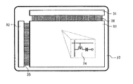
本発明の2つめの例は、前記のような表示回路部(アクティブマトリクス)とその駆動回路(周辺回路)とを有する装置において、駆動回路をCMOS回路とすることである。この場合、回路の全てがCMOSである必要はないが、トランスミッションゲイトやインバータ回路はCMOS化されるのが望ましい。そのような装置の概念図を図3に示した。図には絶縁基板37上にデータドライバー31とゲイトドライバー32が構成され、また、中央部にPMOSのTFTを有するアクティブマトリクス33が構成され、これらのドライバー部とアクティブマトリクスとがゲイト線35、データ線36によって接続された表示装置が示されている。アクティブマトリクス33はPMOSを有する画素セル34の集合体である。
【0030】
CMOS回路に関しては、例えば、得られたTFTのしきい値電圧が、NMOSでは2V、PMOSでは6V、さらにリーク電流がNMOSの方がPMOSよりも10倍以上も多くてもCMOSインバータでは全く支障がない。
【0031】
というのも、インバータのような論理回路ではリークによる消費電力はさほど問題とされないからである。また、インバータの動作は、低電圧状態はNMOSのしきい値電圧以下、高電圧状態はドレイン電圧とPMOSのしきい値電圧(<0)の和以上であることが要求されるが、この場合はドレイン電圧が8V以上、理想的には10V以上あれば問題はなく、例えば、入力は0Vと8Vの2値とすれば十分である。
【0032】
本発明の3つめの例はDRAMのような半導体メモリーに関するものである。半導体メモリー装置は、単結晶ICでは既に速度の限界に達している。これ以上の高速動作をおこなわせるには、トランジスタの電流容量をより大きくすることが必要であるが、それは消費電流の一段の増加の原因になるばかりではなく、特にキャパシタに電荷を蓄えることによって記憶動作をおこなうDRAMに関しては、キャパシタの容量をこれ以上、拡大できない以上、駆動電圧を上げることによって対応するしか方法がない。
【0033】
単結晶ICが速度の限界に達したといわれるのは、一つには基板と配線の容量によって、大きな損失が生じているからである。もし、基板に絶縁物を使用すれば、消費電流をあげなくとも十分に高速な駆動が可能である。このような理由からSOI(絶縁物上の半導体)構造のICが提案されている。
【0034】
DRAMにおいても、1Tr/セル構造の場合には、先の液晶表示装置と回路構成がほとんど同じであり、それ以外の構造のDRAM(例えば、3Tr/セル構造)でも、記憶ビット部のTFTにリーク電流の小さいPMOSのTFTを使用する。基本的なブロック構成は図3のものと同じである。例えば、DRAMにおいては、31がコラムデコーダー、32がローデコーダー、33が記憶素子部、34が単位記憶ビット、35がビット線、36がワード線、37が(絶縁)基板である。
【0035】
液晶表示装置のアクティブマトリクスもDRAMも、いずれもリフレッシュ動作を必要とするものであるが、そのリフレッシュの期間の間には、画素の容量やキャパシタの容量に蓄積された電荷が放電してしまわないように、TFTが十分に大きな抵抗として機能する必要がある。もし、この場合にNMOSのTFTを用いたならば、リーク電流が大きいために十分な駆動ができない。リーク電流の低いPMOSのTFTを用いる利点はここにある。
【0036】
本発明では、高温プロセスのTFTでも有効であるが、特に有効なのは低温プロセスのTFTである。低温プロセスで得られたTFTは、その活性層の組織構造がアモルファスと単結晶の中間であり、また、格子歪みが大きく、いわゆるセミアモルファス状態で、したがって、物性的にアモルファス状態に近い。すなわち、純粋なシリコン材料によって低温プロセスで作製した活性層は、大抵の場合、N− 型である。
【0037】
ここで、セミアモルファス状態について詳細な説明を加えると、アモルファス状態のシリコンは熱を加えるにしたがって結晶成長を始めるが、大気圧下では650℃程度までは、結晶成長という状態ではない。すなわち、結晶性のよい部分の間に比較的結晶性のわるい部分が存在し、しかも分子間の結合がタイトであり、通常のイオン結晶における結晶析出とはことなった様相を示す。すなわち、不対結合手(ダングリングボンド)は極めて少ないことが特徴である。もし、結晶成長が680℃を越えると結晶の成長速度が著しく促進され、多くの結晶粒からなる多結晶状態となる。そして、この場合には、それまで格子歪みによって緩衝されていた結晶粒界の分子結合が破壊されて、粒界部にダングリングボンドが多数形成される。
【0038】
さて、このようなセミアモルファス状態の材料では、活性層へ不純物をドーピングしたとしても、アモルファスシリコンの場合と同様にあまり活性化には寄与しない。その原因としては、本発明人等はドーパント不純物が特にダングリングボンドの多い箇所に選択的にトラップされるためではないかと考えている。したがって、セミアモルファス状態の活性層、もしくは低温プロセスによって形成された活性層では、ドーピングによるしきい値電圧の制御は困難である。
【0039】
また、本発明は、本発明人等の発明である特願平4−73315に記述されるような2層の活性層を有するTFTにおいても有効である。このTFTでは、基板側にアモルファス状態の活性層を設け、その上にセミアモルファス、あるいは多結晶状態の活性層を設けるもので、基板と活性層の界面に存在する電荷によって発生するリークを極限まで減らすことができる。しかしながら、構造上、アモルファスシリコンを用いるために、下側の活性層はN− 型である。したがって、界面に起因するリークは減らせても、この活性層に起因するリークはなかなか減らせない。例えば、PMOSではリーク電流が10−12 A以下(ドレイン電圧1V)であっても、NMOSでは、リーク電流がその100倍以上であった。
【0040】
その作製方法は図4に例示される。まず、基板41上に、窒化珪素等のパッシベーション力の強い皮膜42を形成する。基板が十分に清浄であれば、このような皮膜を形成しなくともよい。さらに下地酸化膜43を形成する。そして、アモルファスシリコン膜を2層形成するが、その堆積速度や堆積基板温度を最適化することによって、後の熱処理によってアモルファス状態のままであるか、セミアモルファス化あるいは多結晶化するかが決定される。この例では上の層45、47がセミアモルファス化(もしくは多結晶化)し、下の層44、47はアモルファスのままである。
【0041】
このような方法の特徴は、同一のチャンバーを用いて成膜をおこないながらも、その条件を微妙に変化させることによって2種の性質の異なるシリコン膜が形成できることにあり、不純物添加によるしきい値電圧制御は、この方法の利点をつぶすこととなる。もし、下の層44、46をN− 型からI型にまで変えようとしても、この層はアモルファスのままであるので、イオン化率が悪く、多量のドーピングが必要である。したがって、チャンバーがこれらの不純物によって著しく汚染され、逆にPMOSの活性層をP型にしてしまう可能性を有している。したがって、このような2層構造の活性層を有するTFTは、ドーピングによるしきい値電圧制御を必要としない本発明に極めて適している。このようなTFTの形成方法は実施例において詳述する。
【0042】
【実施例】
〔実施例1〕 図4に本発明を用いたCMOS回路の作製実施例を説明する。本実施例では基板41としてコーニング社の7059番ガラス基板を使用した。基板はこの他にも様々な種類のものを使用することができるが、半導体被膜中にナトリウム等の可動イオンが侵入しないように基板に応じて対処しなければならない。理想的な基板はアルカリ濃度の小さい合成石英基板であるが、コスト的に利用することが難しい場合には、市販の低アルカリガラスもしくは無アルカリカラスを使用することとなる。本実施例では、基板41上には基板からの可動イオンの侵入を阻止する目的で、厚さ5〜200nm、例えば10nmの窒化珪素膜42を減圧CVD法で形成した。さらに、窒化珪素膜上に、スパッタ法によって、厚さ20〜1000nm、例えば50nmの酸化珪素膜43を形成した。これらの被膜の膜厚は、可動イオンの侵入の程度、あるいは活性層への影響の程度に応じて設計される。
【0043】
例えば、窒化珪素膜42の質が良くなく、電荷のトラップが大きい場合には、酸化珪素膜を通して上の半導体層に影響を及ぼすので、その場合には酸化珪素膜43を厚くする必要がある。
【0044】
これらの皮膜の形成には、上記のような減圧CVD法やスパッタ法だけでなく、プラズマCVD法等の方法によって形成してもよい。特に酸化珪素膜の形成には、TEOSを利用してもよい。それらの手段の選択は投資規模や量産性等を考慮して決定すればよい。これらの被膜は連続的に成膜されてもよいことはいうまでもない。
【0045】
その後、減圧CVD法によって、モノシランを原料として、厚さ20〜200nm、例えば100nmのアモルファスシリコン膜を形成した。基板温度は430〜480℃、例えば450℃とした。さらに、連続的に基板温度を変化させ、520〜560℃、例えば550℃で、厚さ5〜200nm、例えば10nmのアモルファスシリコン膜を形成した。基板温度は後の結晶化の際に重要な影響を与えることが本発明人等の研究の結果、明らかにされた。例えば、480℃以下で成膜したものは結晶化させることが難しかった。逆に520℃以上の温度で成膜したものは結晶化しやすかった。このようにして得られたアモルファスシリコン膜は、600℃で24時間熱アニールした。その結果、上部のシリコン膜のみが結晶化し、いわゆるセミアモルファスシリコンと言われる結晶性シリコンを得た。一方、下部のシリコン膜はアモルファス状態のままであった。
【0046】
上部のシリコン膜の結晶化を促進するためには膜中に含まれている炭素、窒素、酸素の濃度は、いずれも7×1019cm−3以下であることが望ましい。本実施例では、SIMS分析によって1×1017cm−3以下であることを確認した。逆に下部のシリコン膜の結晶化を抑制するためにはこれらの元素が多く含まれていると都合がよい。しかし、過剰なドーピングは半導体特性、ひいてはTFT特性に悪影響を与えるので、ドーピングの有無やその量はTFTの特性に応じて設計される。
【0047】
さて、アモルファスシリコン膜を熱アニールによって、結晶性シリコン膜としたのち、これを適当なパターンにエッチングして、NTFT用の島状半導体領域45とPTFT用の島状半導体領域47とを形成する。各島状半導体領域の上部には、意図的な不純物ドープはされず、特にボロン等の不純物濃度は1017cm−3以下であることをSIMS(2次イオン質量分析法)によって確認した。したがって、この部分の導電型は、N− 型であると推測される。一方、各半導体領域の下部のシリコン層44、46は実質的にアモルファスシリコンであった。
【0048】
その後、酸素雰囲気中での酸化珪素をターゲットとするスパッタ法によって、ゲイト絶縁膜(酸化珪素)48を厚さ50〜300nm、例えば100nmだけ形成した。この厚さは、TFTの動作条件等によって決定される。
【0049】
次にスパッタ法によって、アルミニウム皮膜を厚さ500nmだけ形成し、これを混酸(5%の硝酸を添加した燐酸溶液)によってパターニングし、ゲイト電極・配線49および50を形成した。エッチングレートは、エッチングの温度を40℃としたときに225nm/分であった。このようにして、TFTの外形を整えた。このときのチャネルの大きさは、いずれも長さ8μm、幅20μmとした。このときの状態を図4(A)に示す。
【0050】
さらに、陽極酸化法によってアルミニウム配線の表面に酸化アルミニウムを形成した。陽極酸化の方法としては、本発明人等の発明である特願平3−231188もしくは特願平3−238713に記述される方法を用いた。詳細な実施の様態については、目的とする素子の特性やプロセス条件、投資規模等によって変更を加えればよい。本実施例では、陽極酸化によって、厚さ250nmの酸化アルミニウム被膜51および52を形成した。
【0051】
その後、ゲイト酸化膜を通したイオン注入法によって、公知のCMOS作製技術を援用し、N型ソース/ドレイン領域53とP型ソース/ドレイン領域54を形成した。いずれも不純物濃度は8×1019cm−3となるようにした。イオン源としては、P型はフッ化ホウ素イオンを、N型はリンイオンを用い、前者は加速電圧80keVで、後者は加速電圧110keVで注入した。加速電圧はゲイト酸化膜の厚さや半導体領域45、47の厚さを考慮して設定される。イオン注入法のかわりに、イオンドーピング法を用いてもよい。イオン注入法では注入されるイオンは質量によって分離されるので、不必要なイオンは注入されることがないが、イオン注入装置で処理できる基板の大きさは限定される。一方、イオンドーピング法では、比較的大きな基板(例えば対角30インチ以上)も処理する能力を有するが、水素イオンやその他不必要なイオンまで同時に加速されて注入されるので、基板が加熱されやすい。この場合にはイオン注入法で使用するようなフォトレジストをマスクとした選択的な不純物注入は難しい。
【0052】
このようにして、オフセット領域を有するTFTが作製された。その様子を図4(B)に示す。最後に、レーザーアニール法によって、ゲイト電極部をマスクとしてソース/ドレイン領域の再結晶化をおこなった。レーザーアニールの条件は、例えば特願平3−231188や同3−238713に記述されている方法を使用した。そして層間絶縁物55として、酸化珪素をRFプラズマCVD法で形成し、これに電極形成用の穴を開け、アルミニウム配線56〜48を形成して、素子を完成させた。
【0053】
本実施例では、レーザーアニールによって、もともと結晶性シリコンであった、被膜45、47のみならず、アモルファスシリコンであった被膜44、46までもが結晶化される。これは、レーザーアニールが強力だからである。その結果、図4(C)に示すように初期のアモルファス領域44、46はチャネルの下の部分59、60以外は全てソース/ドレインとおなじ結晶性を有する材料に変換されてしまった。その結果、ソース/ドレインの厚さは島状半導体領域45、47と実質的に同じとなった。しかしながら、実質的なチャネルの厚さは図から明らかなように、約10nmというようにソース/ドレイン領域よりも薄かった。その結果、ソース/ドレインのシート抵抗は小さく、また、チャネルが薄い分だけOFF電流が少ないという優れた特性を示すことができた。
【0054】
図4には液晶表示装置の駆動回路に使用されるCMOS回路の作製工程を示したが、同じ基板上のアクティブマトリクス部には、PMOSが同じように形成されている。このようにして形成されたTFTの特性は、チャネル長が5μm、チャネル幅が20μmで、ソース/ドレイン電圧が1Vの状態で、NMOSのリーク電流は〜100pA、PMOSはPMOSの〜1pAであった。このようにオフ抵抗はPMOSの方が100倍も大きかった。また、ゲイト電圧が+8V(PMOSの場合は−8V)のオン状態では、NMOSは10μA、PMOSは100nAの電流を流した。PMOSのドレイン電流がNMOSに比べて著しく小さいのは、しきい値電圧がPMOSの場合には、負にシフトしているからである。したがって、PMOSのゲイト電圧を−12Vとしたときには、ドレイン電流は1μAとなった。すなわち、このようなTFTを用いて、トランスミッションゲイトを構成せんとすれば、PTFTに印加する電位を負の方にシフトさせるべきである。
【0055】
アクティブマトリクス部のPMOSのTFTの大きさは、チャネル長5μm、チャネル幅10μmとした。アクティブマトリクスとして利用されたPMOSのTFTのゲイト電圧を0Vから−12Vまで変化させると、ドレイン電流は106 倍にまで増大するので、画像表示用としては問題がなかった。さらに、大きく変動させることが必要な場合にはPMOSのTFTを2つ直列に構成して、いわゆるデュアルゲイト構造とするとよい。この場合には、オフ状態では、TFTの抵抗はさらに約1桁上昇するものの、ON状態では、TFTの抵抗は2倍程度にしかならないので、結局、ドレイン電流は107 も変動することとなる。TFTを3段直列に形成したら、さらに変動率は1桁増加する。
【0056】
〔実施例2〕 図5には、本発明を実施するためのNMOSおよびPMOS素子の作製工程を示す。本実施例では、高温プロセスによるTFTを作製した。まず、石英基板61(幅105mm×長さ105mm×厚さ1.1mm)上に、減圧CVD法によって、不純物のドープされていないポリシリコン膜を厚さ100〜500nm、好ましくは150〜200nm形成した。そして、これを乾燥した高温の酸素雰囲気中で酸化せしめた。温度は850〜1100℃の範囲とし、950〜1050℃が特に好ましかった。このようにして、基板上に酸化珪素膜62を形成した(図5(A))。
【0057】
さらに、ジシランを原料とするプラズマCVD法もしくは減圧CVD法によってアモルファスシリコン膜を厚さ100〜1000nm、好ましくは、350〜700nm形成した。基板温度は350〜450℃とした。そして、これを550〜650℃、このましくは580〜620℃で長時間アニールして、結晶性を持たせた。そして、これをパターニングして、図5(B)に示すようにNMOSの領域63aとPMOSの領域63bを形成した。
【0058】
ついで、乾燥した高温の酸化雰囲気中で上記シリコン領域63の表面を酸化して、図5(C)に示すように、シリコン領域の表面に厚さ50〜150nm、好ましくは50〜70nmの酸化珪素膜64を形成した。酸化条件は、酸化珪素62と同じとした。
【0059】
その後、リンが1019〜2×1020cm−3、例えば8×1019cm−3ドープされたシリコン膜を厚さ200〜500nm、好ましくは350〜400nmだけ形成し、これを図5(D)のようにパターニングして、NMOSのゲイト65aおよびPMOSのゲイト65bを形成した。さらに、イオン注入法によって、NMOSおよびPMOSの不純物領域66および67をそれぞれ形成した。
【0060】
このとき、これらの不純物の底面は下地の酸化珪素膜62に達しないようにした。すなわち、下地の酸化膜とシリコン膜の界面には多くの局在準位が形成され、結果として、下地の酸化膜付近のシリコン膜は特定の導電型(通常の場合はN型)を示す。もし、不純物領域が、このような部分のシリコン膜に隣接していた場合には、リークが生じる。したがって、このようなリークを避けるために、本実施例では不純物領域の底面と下地酸化膜62の間に50〜200nmの空間を設けた。
【0061】
本実施例では、酸化珪素膜64を通してイオン注入をおこなったが、より精密に不純物領域の深さを制御するためには、酸化珪素膜64を除去して、熱拡散をおこなってもよい。
【0062】
不純物領域を形成した後、熱アニールによって、不純物領域の結晶性を回復させた。その後は通常のTFTの作製工程と同様に、層間絶縁物(リンボロンガラス)68を堆積して、リフローによって平坦化させ、コンタクトホールを形成して金属配線69〜71を形成した。
【0063】
以上の工程によって形成された、TFTを使用して、1Tr/セルのDRAM(16kビット)を作製した。TFTのチャネル部の大きさをチャネル長2μm、チャネル幅10μmとしたときの、NMOSのリーク電流は、ソース/ドレイン電圧が1Vのときに、約10pA、PMOSのリーク電流は、同じ条件で約0.1pAであった。メモリー素子部はチャネル長2μm、チャネル幅2μmのPMOSを使用した。メモリー素子部のキャパシタの容量は0.5pFとし、リフレッシュ周期は最大5秒という長時間の記憶保持が可能となった。これは、PMOSのオフ状態の抵抗が5×1013Ωという高い値であったため可能となった。また、周辺回路は、上記の工程で作製したNMOSとPMOSを使用して、CMOS化した。このような絶縁基板上のDRAMであるので、高速動作が可能であり、ビットあたり100nsecで書込み・読出が可能であった。
【0064】
【発明の効果】
本発明によって、特にダイナミックな回路およびそのような回路を有する装置の信頼性と性能を高めることができた。従来、特に液晶表示装置のアクティブマトリクスのような目的に対しては多結晶TFTはON/OFF比が低く、実用化にはさまざまな困難があったが、本発明によってそのような問題はほぼ解決されたと思われる。さらに、実施例2に示したように絶縁基板上の半導体回路は高速動作という点で優れている。実施例では示さなかったが、単結晶半導体集積回路の立体化の手段として用いられるTFTにおいても本発明を実施することによって効果を挙げられることは明白であろう。
【0065】
例えば、周辺論理回路を単結晶半導体上の半導体回路で構成し、その上に層間絶縁物を介してTFTを設け、これによってメモリー素子部を構成することもできる。この場合には、メモリー素子部をPMOSのTFTを使用したDRAM回路とし、その駆動回路は単結晶半導体回路にCMOS化されて構成されている。しかも、このような回路をマイクロプロセッサーに利用した場合には、メモリー部を2階に上げることになるので、面積を節約することができる。このように本発明は産業上、極めて有益な発明であると考えられる。
【図面の簡単な説明】
【図1】NMOSのTFTの動作の概念図を示す。
【図2】PMOSのTFTの動作の概念図を示す。
【図3】本発明の構成の概念図を示す。
【図4】本発明のTFTの作製工程を示す。
【図5】本発明のTFTの作製工程を示す。
【符号の説明】
11、21・・・ゲイト電極
12、22・・ソース領域
13、23・・ドレイン領域
14、24・・・活性層
15、25・・・チャネル
16、26・・・反転層
31・・・データドライバー(DRAMの場合にはコラムデコーダー)
32・・・ゲイトドライバー(DRAMの場合はローデコーダー)
33・・・アクティブマトリクス部(DRAMの場合は記憶素子部)
34・・・単位画素(DRAMの場合は単位記憶ビット)
35・・・ゲイト線(DRAMの場合はビット線)
36・・・データ線(DRAMの場合はワード線)
37・・・絶縁基板[0001]
[Industrial applications]
The present invention relates to a MOS-type or MIS (metal-insulator-semiconductor) -type field-effect element as a switching element, such as a liquid crystal display device or a dynamic RAM (DRAM). The present invention relates to a matrix device (including an electro-optical display device and a semiconductor memory device) having dynamic operation and a driving circuit therefor. In particular, the present invention relates to an apparatus using a thin-film semiconductor element such as a thin-film semiconductor transistor formed on an insulating substrate as a MOS element.
[0002]
[Prior art]
In recent years, studies have been made on an insulated gate semiconductor device having a thin-film active layer (also referred to as an active region) on an insulating substrate. In particular, a thin film insulated gate transistor, a so-called thin film transistor (TFT), has been enthusiastically studied. These are intended to be used for controlling each pixel in a display device such as a liquid crystal having a matrix structure, and are distinguished as amorphous silicon TFT or polycrystalline silicon TFT depending on the material and crystal state of the semiconductor used. Have been. However, recently, research has been made on using a material exhibiting an intermediate state between polycrystalline silicon and amorphous. This material is called semi-amorphous, and is considered to be a state in which small crystals are floating in an amorphous structure. This material is an excellent material having the characteristics of high mobility in a single crystal state and low leakage current in an amorphous state, as described later.
[0003]
Also in a single crystal silicon integrated circuit, a polycrystalline silicon TFT is used as a so-called SOI technology, and this is used as a load transistor in, for example, a highly integrated SRAM. However, in this case, the amorphous silicon TFT is hardly used.
[0004]
Further, in a semiconductor circuit on an insulating substrate, since there is no capacitive coupling between the substrate and the wiring, an extremely high-speed operation is possible, and a technology for using as an ultra-high-speed microprocessor or an ultra-high-speed memory has been proposed.
[0005]
In general, the electric field mobility of a semiconductor in an amorphous state is small, and therefore, it cannot be used for a TFT requiring high-speed operation. Further, in the case of amorphous silicon, since the P-type electric field mobility is extremely small, a P-channel TFT (PMOS TFT) cannot be manufactured. Therefore, in combination with an N-channel TFT (NMOS TFT), A complementary MOS circuit (CMOS) cannot be formed.
[0006]
However, a TFT formed of an amorphous semiconductor has a feature that an OFF current is small. Therefore, unlike a transistor of an active matrix of a liquid crystal, such a high speed operation is not required, and only one conductivity type is sufficient, and it is used for an application that requires a TFT having a high charge retention ability. .
[0007]
On the other hand, a polycrystalline semiconductor has a higher electric field mobility than an amorphous semiconductor, and thus can operate at high speed. For example, in a TFT using a silicon film recrystallized by laser annealing, the electric field mobility is 300 cm. 2 / Vs. The electric field mobility of a MOS transistor formed on a normal single crystal silicon substrate is 500 cm. 2 / Vs, which is an extremely large value. The operating speed of the MOS circuit on single crystal silicon is limited by the parasitic capacitance between the substrate and the wiring, whereas the MOS circuit on the single crystal silicon is on an insulating substrate. There is no such restriction, and remarkable high-speed operation is expected.
[0008]
Further, in the case of polycrystalline silicon, not only NMOS TFTs but also PMOS TFTs can be obtained in the same manner, so that a CMOS circuit can be formed. For example, in an active matrix type liquid crystal display device, if only the active matrix portion is provided, In addition, a circuit having a so-called monolithic structure in which peripheral circuits (drivers and the like) are also formed of CMOS polycrystalline TFTs is known.
[0009]
The TFT used in the above-described SRAM also pays attention to this point, and the PMOS is configured by a TFT and is used as a load transistor.
[0010]
In a normal amorphous TFT, it is difficult to form a source / drain region by a self-alignment process as used in a single-crystal IC technology, and it is difficult to form a gate electrode and a source / drain region by geometrical overlap. While the parasitic capacitance becomes a problem, the polycrystalline TFT can adopt a self-aligned process, and thus has a feature that the parasitic capacitance is remarkably suppressed.
[0011]
[Problems to be solved by the invention]
Several problems have been pointed out with respect to the advantages of the polycrystalline TFT having such characteristics. A general polycrystalline TFT is a coplanar type having an active layer formed on an insulating substrate and having a gate insulating film and a gate electrode thereon. Although this structure has an advantage that a self-alignment process can be adopted, it is difficult to reduce a leak current (OFF current) of the active layer.
[0012]
Although the details of the cause of the leak current are not clear, the major cause was the interface charge generated between the underlayer and the active layer. Therefore, this problem was solved by paying close attention to the fabrication of this interface and reducing the interface state density to the same level as that between the gate oxide film and the active layer.
[0013]
That is, in a high-temperature process (maximum process temperature of about 1000 ° C.), quartz is used as a substrate, a silicon film is formed thereon, and this is thermally oxidized at about 1000 ° C. to obtain a clean surface. After the formation, an active silicon layer was formed by a film forming method such as a low pressure CVD method.
[0014]
In a low-temperature process (a process having a maximum process temperature of 650 ° C. or lower; also referred to as a medium-temperature process), a silicon oxide film having a low interface state density as low as a gate insulating film is formed between a substrate and an active layer as a base film. Was adopted. As a method for forming the silicon oxide film, a sputtering method is excellent. In addition, an oxide film having excellent characteristics can be obtained by an ECR-CVD method or a TEOS plasma CVD method.
[0015]
However, the leakage current could not be improved. In particular, the NMOS was one order of magnitude larger than the PMOS. The present inventors have speculated that the cause is that the active layer is a weak N-type. Actually, a phenomenon in which the threshold voltages of the PMOS and NMOS fabricated in the high-temperature process and the low-temperature process shift in the negative direction was observed with good reproducibility. It is presumed that this is because, in particular, when silicon has a high purity and no other impurities are added, if the crystallinity is not good like amorphous silicon, the silicon becomes a weak N-type. It is speculated that high-temperature process polycrystalline silicon has many lattice defects and dangling bonds, unlike perfect single-crystal silicon, and these electrons serve as donors to supply electrons. Of course, the possibility of the influence of a small amount of contaminating elements (such as sodium) remains.
[0016]
In any case, if such a cause exists, it can be explained that the threshold voltage of the NMOS is significantly lower than that of the PMOS and the leakage current is large. This is shown in FIG. In the NMOS, as shown in FIG. + Ground) and drain 13 (N + The threshold voltage V is applied to the gate electrode 11 while a positive voltage is applied to the th When a voltage higher than that is applied, a channel is formed on the gate electrode side of the
[0017]
If the potential of the gate electrode is equal to the threshold voltage V th Even in the following state, the current indicated by the dotted line is flowing. When the potential of the gate electrode becomes a large negative value, an inversion layer (P type) 16 is generated as shown in FIG. 1B, but the entire channel does not reach the inversion, and conversely, an excessive voltage is applied. Then, electrons are accumulated on the opposite side of the gate, and a channel is formed. The actually obtained NMOS data is consistent with this consideration.
[0018]
On the other hand, in the PMOS, the active layer is N − The threshold voltage increases because of the type. However, the leakage on the other side of the gate is greatly reduced. FIG. 2 shows a case where a voltage lower than the threshold or a voltage higher than the threshold is applied to the PMOS.
[0019]
Such a remarkable leak current in the NMOS has been an obstacle in various application fields, particularly in fields requiring dynamic operation. For example, in a liquid crystal active matrix or a DRAM, image information or stored information is lost due to leakage current. Therefore, it was necessary to reduce such a leak current.
[0020]
One method is to make the active layer of the NMOS intrinsic (I-type) or weak P-type. For example, when an appropriate amount of P-type impurity (for example, boron) is implanted into only the NMOS or both the NMOS and the PMOS at the time of forming the active layer, the active layer of the NMOS is made I-type or weak P-type. The threshold voltage should increase and the leakage current should also decrease significantly. However, this method has several problems.
[0021]
Usually, a CMOS circuit in which both an NMOS and a PMOS are mounted on one substrate is used. However, if an impurity is implanted only into the N-type, an extra photolithography step is required. Further, if a p-type impurity is to be implanted into both the active layers of the NMOS and the PMOS, a delicate impurity implantation technique is required. If the injection amount is too large, the threshold voltage of the PMOS will decrease, and the leakage current will increase.
[0022]
Ion implantation technology is also a problem. In the implantation technique for performing mass separation, it is possible to implant only necessary impurity elements, but the processing area is small. In addition, although the processing area is large in the so-called ion doping method, unnecessary ions are also implanted because there is no mass separation step, and the doping amount may not be accurate.
[0023]
In addition, such a method in which ions are accelerated and implanted causes a localized level to be formed at the interface between the active layer and the base. Further, unlike the conventional ion implantation for a single crystal semiconductor, since the implantation is performed on an insulating substrate, the charge-up phenomenon is remarkable, and it is difficult to precisely control the implantation amount.
[0024]
Therefore, it is conceivable to mix P-type impurities in advance when forming the active layer. However, it is difficult to control the amount of trace impurities, and when forming NMOS and PMOS from the same film, If the amount is not appropriate, the leakage current of the PMOS increases, and if the NMOS and the PMOS are formed from different films, an additional mask process is required. Controlling the threshold voltage by such a method also causes variation in the threshold value of the TFT due to factors such as the gas flow rate, and the variation in the threshold value for each lot becomes extremely large.
[0025]
The present invention seeks to provide a solution to such a difficult problem, but the main point is that the process does not reduce the leakage current of the NMOS but optimizes the circuit design. Thus, a circuit that can be used even with a TFT having a large leak current is designed. As described above, when the active layer is formed from a high-purity silicon material, N − The energy level is extremely reproducible and stable. Further, the process itself is extremely simple, and the yield is sufficiently high. On the other hand, various methods for controlling the threshold voltage not only complicate the process, but also vary the energy level (Fermi level, etc.) of the obtained active layer for each lot, and lower the yield. I do.
[0026]
Obviously, rather than adapting the NMOS to the circuit by improving the process, 17 cm -3 A process in which impurities are eliminated as much as possible is easier than performing a delicate doping to the extent possible, and it is better to design a circuit in accordance with the resulting NMOS. Here is the technical idea of the present invention.
[0027]
[How to solve the problem]
The semiconductor circuit to which the present invention is applied is not universal. The present invention particularly uses a material such as a liquid crystal display device, whose light transmittance and reflectivity change due to the effect of an electric field, sandwiches these materials between opposing electrodes, and applies an electric field between the opposing electrodes. An active matrix circuit for displaying images, a memory device such as a DRAM that stores data by storing electric charges in a capacitor, a MOS transistor having a MOS structure as a capacitor, or another capacitor. It is suitable for a circuit having a dynamic circuit such as a dynamic shift register for driving a next stage circuit. In particular, the present invention is suitable for a circuit in which a dynamic circuit and a static circuit are mixed.
[0028]
One example of the present invention is to use a PMOS TFT as a switching transistor in a display portion of an active matrix circuit such as a liquid crystal. Here, it is necessary that the PMOS TFT is inserted in series with the data line and the pixel electrode, and if the NMOS TFT is inserted in parallel, the purpose of the display is as if there is a large leak current. Is inappropriate for Therefore, the present invention includes a case where PMOS and NMOS TFTs are inserted in series in a pixel TFT circuit. Of course, it is within the technical scope of the present invention that two PMOS TFTs are inserted in parallel.
[0029]
A second example of the present invention is that a driving circuit is a CMOS circuit in an apparatus having the above-described display circuit section (active matrix) and its driving circuit (peripheral circuit). In this case, not all of the circuits need to be CMOS, but it is desirable that the transmission gate and the inverter circuit be CMOS. FIG. 3 shows a conceptual diagram of such an apparatus. In the figure, a
[0030]
As for the CMOS circuit, for example, even if the obtained threshold voltage of the TFT is 2 V for the NMOS, 6 V for the PMOS, and the leakage current is 10 times or more that of the NMOS than that of the PMOS, there is no problem in the CMOS inverter. Absent.
[0031]
This is because, in a logic circuit such as an inverter, power consumption due to leakage is not a significant problem. The operation of the inverter is required to be lower than the threshold voltage of the NMOS in the low voltage state and higher than the sum of the drain voltage and the threshold voltage (<0) of the PMOS in the high voltage state. There is no problem if the drain voltage is 8 V or more, ideally 10 V or more. For example, it is sufficient if the input is a binary value of 0 V and 8 V.
[0032]
The third example of the present invention relates to a semiconductor memory such as a DRAM. Semiconductor memory devices have already reached their speed limits with single crystal ICs. To operate at higher speeds than this, it is necessary to increase the current capacity of the transistor, but this not only causes a further increase in current consumption, but also, in particular, stores the charge by storing the charge in the capacitor. For a DRAM that operates, the only way to deal with this is by increasing the drive voltage, as the capacity of the capacitor cannot be increased any further.
[0033]
It is said that single crystal ICs have reached the speed limit because, in part, large losses are caused by the capacitance of the substrate and the wiring. If an insulator is used for the substrate, sufficiently high-speed driving can be performed without increasing current consumption. For such a reason, an IC having an SOI (semiconductor on insulator) structure has been proposed.
[0034]
In the case of a DRAM, in the case of a 1Tr / cell structure, the circuit configuration is almost the same as that of the above-described liquid crystal display device. A PMOS TFT with a small current is used. The basic block configuration is the same as that of FIG. For example, in a DRAM, 31 is a column decoder, 32 is a row decoder, 33 is a storage element unit, 34 is a unit storage bit, 35 is a bit line, 36 is a word line, and 37 is an (insulated) substrate.
[0035]
Both the active matrix and the DRAM of the liquid crystal display device require a refresh operation, but during the refresh period, the charges stored in the pixel capacitance and the capacitor capacitance are not discharged. Thus, the TFT needs to function as a sufficiently large resistor. If an NMOS TFT is used in this case, sufficient driving cannot be performed due to a large leak current. This is an advantage of using a PMOS TFT having a low leakage current.
[0036]
In the present invention, a TFT of a high temperature process is effective, but a TFT of a low temperature process is particularly effective. The TFT obtained by the low-temperature process has an active layer having an intermediate structure between an amorphous layer and a single crystal layer, and has a large lattice distortion, and is in a so-called semi-amorphous state. That is, an active layer made of a pure silicon material by a low-temperature process usually has N − Type.
[0037]
Here, a detailed description of the semi-amorphous state will be given. Silicon in the amorphous state starts crystal growth as heat is applied, but does not reach a state of crystal growth up to about 650 ° C. under atmospheric pressure. That is, there is a portion having relatively poor crystallinity between the portions having good crystallinity, and the bonds between the molecules are tight, which shows a different aspect from the crystal precipitation in a normal ionic crystal. That is, it is characterized in that the number of dangling bonds is extremely small. If the crystal growth exceeds 680 ° C., the growth rate of the crystal is remarkably accelerated, and a polycrystalline state composed of many crystal grains is obtained. In this case, the molecular bonds at the crystal grain boundaries that have been buffered by the lattice distortion are broken, and a large number of dangling bonds are formed at the grain boundaries.
[0038]
Now, in such a semi-amorphous material, even if the active layer is doped with impurities, it does not contribute much to activation as in the case of amorphous silicon. The inventor of the present invention thinks that the cause is that the dopant impurities are selectively trapped particularly in a portion having many dangling bonds. Therefore, in an active layer in a semi-amorphous state or an active layer formed by a low-temperature process, it is difficult to control the threshold voltage by doping.
[0039]
The present invention is also effective in a TFT having two active layers as described in Japanese Patent Application No. 4-73315 which is an invention of the present inventors. In this TFT, an active layer in an amorphous state is provided on the substrate side, and an active layer in a semi-amorphous or polycrystalline state is provided on the active layer. The leakage generated by the charge existing at the interface between the substrate and the active layer is minimized. Can be reduced. However, due to the structure of amorphous silicon, the lower active layer is N − Type. Therefore, even though the leakage due to the interface can be reduced, the leakage due to the active layer cannot be easily reduced. For example, in a PMOS, the leakage current is 10 -12 Even at A (drain voltage 1 V), the leakage current was 100 times or more of the NMOS.
[0040]
The manufacturing method is illustrated in FIG. First, a
[0041]
The feature of such a method is that while film formation is performed using the same chamber, a silicon film having two different properties can be formed by subtly changing the conditions. Voltage control will undermine the advantages of this method. If the
[0042]
【Example】
Embodiment 1 FIG. 4 illustrates an embodiment of manufacturing a CMOS circuit using the present invention. In this embodiment, a Corning 7059 glass substrate was used as the
[0043]
For example, when the quality of the
[0044]
These films may be formed not only by the above-described low pressure CVD method or sputtering method but also by a method such as a plasma CVD method. In particular, TEOS may be used for forming the silicon oxide film. The selection of these means may be determined in consideration of investment scale, mass productivity, and the like. Needless to say, these films may be formed continuously.
[0045]
Thereafter, an amorphous silicon film having a thickness of 20 to 200 nm, for example, 100 nm was formed by using a monosilane as a raw material by a low pressure CVD method. The substrate temperature was 430 to 480C, for example, 450C. Further, the substrate temperature was continuously changed, and an amorphous silicon film having a thickness of 5 to 200 nm, for example, 10 nm was formed at 520 to 560 ° C., for example, 550 ° C. As a result of the study of the present inventors, it has been revealed that the substrate temperature has an important influence upon the subsequent crystallization. For example, it was difficult to crystallize a film formed at 480 ° C. or lower. Conversely, a film formed at a temperature of 520 ° C. or higher was easily crystallized. The amorphous silicon film thus obtained was thermally annealed at 600 ° C. for 24 hours. As a result, only the upper silicon film was crystallized, and crystalline silicon called semi-amorphous silicon was obtained. On the other hand, the lower silicon film remained in an amorphous state.
[0046]
In order to promote the crystallization of the upper silicon film, the concentration of carbon, nitrogen and oxygen contained in the film should be 7 × 10 19 cm -3 It is desirable that: In this embodiment, 1 × 10 17 cm -3 It was confirmed that: Conversely, in order to suppress crystallization of the lower silicon film, it is convenient that these elements are contained in a large amount. However, excessive doping has an adverse effect on semiconductor characteristics and, consequently, TFT characteristics. Therefore, the presence or absence and the amount of doping are designed according to the TFT characteristics.
[0047]
After the amorphous silicon film is converted into a crystalline silicon film by thermal annealing, the crystalline silicon film is etched into an appropriate pattern to form an island-shaped
[0048]
Thereafter, a gate insulating film (silicon oxide) 48 having a thickness of 50 to 300 nm, for example, 100 nm was formed by a sputtering method using silicon oxide as a target in an oxygen atmosphere. This thickness is determined by the operating conditions of the TFT and the like.
[0049]
Next, an aluminum film having a thickness of 500 nm was formed by a sputtering method, and this was patterned with a mixed acid (a phosphoric acid solution to which 5% nitric acid was added) to form gate electrodes /
[0050]
Further, aluminum oxide was formed on the surface of the aluminum wiring by an anodic oxidation method. As a method of anodic oxidation, a method described in Japanese Patent Application No. 3-231188 or Japanese Patent Application No. 3-238713, which is an invention of the present inventors, was used. A detailed embodiment may be changed depending on the characteristics of the target device, process conditions, investment scale, and the like. In this example,
[0051]
After that, an N-type source /
[0052]
Thus, a TFT having an offset region was manufactured. This is shown in FIG. Finally, the source / drain regions were recrystallized by laser annealing using the gate electrode as a mask. The conditions for laser annealing were, for example, the methods described in Japanese Patent Application Nos. 3-231188 and 3-238713. Then, silicon oxide was formed as an
[0053]
In the present embodiment, not only the
[0054]
FIG. 4 shows a manufacturing process of a CMOS circuit used for a driving circuit of a liquid crystal display device. In the active matrix portion on the same substrate, a PMOS is similarly formed. The characteristics of the TFT thus formed were as follows: the channel length was 5 μm, the channel width was 20 μm, the source / drain voltage was 1 V, the leakage current of the NMOS was 100100 pA, and the PMOS was 11 pA of the PMOS. . As described above, the off-state resistance of the PMOS was 100 times larger. In the ON state where the gate voltage was +8 V (−8 V in the case of a PMOS), a current of 10 μA flowed through the NMOS and a current of 100 nA flowed through the PMOS. The reason why the drain current of the PMOS is significantly smaller than that of the NMOS is that the threshold voltage is negatively shifted in the case of the PMOS. Therefore, when the gate voltage of the PMOS was -12 V, the drain current was 1 μA. That is, if a transmission gate is formed using such a TFT, the potential applied to the PTFT should be shifted to the negative side.
[0055]
The size of the PMOS TFT in the active matrix portion was 5 μm in channel length and 10 μm in channel width. When the gate voltage of the PMOS TFT used as the active matrix is changed from 0V to -12V, the drain current becomes 10 6 Since it increased twice, there was no problem for image display. Further, when a large variation is required, two PMOS TFTs may be configured in series to form a so-called dual gate structure. In this case, in the off state, the resistance of the TFT further increases by about one digit. However, in the on state, the resistance of the TFT is only about twice, so that the drain current eventually becomes 10 times. 7 Will also fluctuate. If the TFTs are formed in three stages in series, the rate of change further increases by one digit.
[0056]
Embodiment 2 FIGS. 5A and 5B show a process of manufacturing an NMOS and a PMOS device for carrying out the present invention. In this example, a TFT was manufactured by a high-temperature process. First, a polysilicon film not doped with impurities is formed on a quartz substrate 61 (width 105 mm × length 105 mm × thickness 1.1 mm) by a low pressure CVD method to a thickness of 100 to 500 nm, preferably 150 to 200 nm. . This was oxidized in a dry high-temperature oxygen atmosphere. Temperatures ranged from 850 to 1100 ° C, with 950 to 1050 ° C being particularly preferred. Thus, the
[0057]
Further, an amorphous silicon film having a thickness of 100 to 1000 nm, preferably 350 to 700 nm was formed by a plasma CVD method or a low pressure CVD method using disilane as a raw material. The substrate temperature was 350-450 ° C. Then, this was annealed at 550 to 650 ° C., preferably 580 to 620 ° C. for a long time to have crystallinity. Then, this was patterned to form an
[0058]
Then, the surface of the silicon region 63 is oxidized in a dry high-temperature oxidizing atmosphere, and a silicon oxide having a thickness of 50 to 150 nm, preferably 50 to 70 nm is formed on the surface of the silicon region as shown in FIG. A
[0059]
Then, phosphorus is 10 19 ~ 2 × 10 20 cm -3 , For example, 8 × 10 19 cm -3 A doped silicon film was formed to a thickness of 200 to 500 nm, preferably 350 to 400 nm, and this was patterned as shown in FIG. 5D to form an
[0060]
At this time, the bottom surfaces of these impurities were prevented from reaching the underlying
[0061]
In this embodiment, the ion implantation is performed through the
[0062]
After forming the impurity regions, the crystallinity of the impurity regions was restored by thermal annealing. After that, an interlayer insulator (phosphorus glass) 68 was deposited and flattened by reflow, and a contact hole was formed to form
[0063]
A 1 Tr / cell DRAM (16 k bits) was manufactured using the TFTs formed by the above steps. When the size of the channel portion of the TFT is 2 μm in channel length and 10 μm in channel width, the leakage current of the NMOS is about 10 pA when the source / drain voltage is 1 V, and the leakage current of the PMOS is about 0 under the same conditions. .1 pA. For the memory element portion, a PMOS having a channel length of 2 μm and a channel width of 2 μm was used. The capacity of the capacitor in the memory element portion was set to 0.5 pF, and the refresh cycle could be held for a long time of 5 seconds at the maximum. This is because the PMOS off-state resistance is 5 × 10 Thirteen This was possible because of the high value of Ω. The peripheral circuit was made CMOS using the NMOS and PMOS fabricated in the above steps. Since the DRAM is on such an insulating substrate, high-speed operation is possible, and writing / reading can be performed in 100 nsec per bit.
[0064]
【The invention's effect】
The present invention has increased the reliability and performance of particularly dynamic circuits and devices having such circuits. Heretofore, polycrystalline TFTs have a low ON / OFF ratio, especially for purposes such as the active matrix of a liquid crystal display device, and have had various difficulties in practical use. However, such problems are almost solved by the present invention. It seems that it was done. Further, as shown in Embodiment 2, the semiconductor circuit on the insulating substrate is excellent in high-speed operation. Although not shown in the examples, it will be apparent that the effects of the present invention can be obtained by implementing the present invention in a TFT used as a three-dimensional means of a single crystal semiconductor integrated circuit.
[0065]
For example, the peripheral logic circuit may be formed of a semiconductor circuit over a single crystal semiconductor, and a TFT may be provided thereover with an interlayer insulator therebetween, thereby forming a memory element portion. In this case, the memory element section is a DRAM circuit using a PMOS TFT, and the driving circuit is formed by converting a single crystal semiconductor circuit into CMOS. Moreover, when such a circuit is used for a microprocessor, the memory section is raised to the second floor, so that the area can be saved. As described above, the present invention is considered to be an industrially extremely useful invention.
[Brief description of the drawings]
FIG. 1 shows a conceptual diagram of the operation of an NMOS TFT.
FIG. 2 shows a conceptual diagram of the operation of a PMOS TFT.
FIG. 3 shows a conceptual diagram of the configuration of the present invention.
FIG. 4 shows a manufacturing process of the TFT of the present invention.
FIG. 5 shows a manufacturing process of the TFT of the present invention.
[Explanation of symbols]
11, 21 ... gate electrode
12, 22, source area
13, 23 ··· Drain region
14, 24 ... active layer
15, 25 ... channel
16, 26 ... inversion layer
31 Data driver (column decoder in case of DRAM)
32 ... Gate driver (row decoder for DRAM)
33: Active matrix section (memory element section in case of DRAM)
34 unit pixel (unit storage bit in case of DRAM)
35 ... Gate line (bit line in case of DRAM)
36 Data line (word line in case of DRAM)
37 ... insulating substrate
Claims (8)
前記絶縁表面上に形成された複数の画素電極と、
前記画素電極に接続され、チャネル形成領域、ソース領域及びドレイン領域を有する均一な厚さの平坦な半導体膜を有する、前記絶縁表面上に形成されたPチャネル型薄膜トランジスタと、
を有する電気光学装置において、
前記チャネル形成領域は前記半導体膜において結晶性半導体からなる上層とアモルファス半導体からなる下層の二層からなり、
前記ソース領域と前記ドレイン領域の厚さは前記半導体膜の厚さと同じであり、
前記チャネル形成領域の前記上層は、厚さが前記ソース領域及び前記ドレイン領域よりも薄いことを特徴とする電気光学装置。A substrate having an insulating surface;
A plurality of pixel electrodes formed on the insulating surface,
A P-channel thin film transistor formed on the insulating surface, the P-channel thin film transistor being connected to the pixel electrode, having a flat semiconductor film having a uniform thickness having a channel formation region, a source region, and a drain region;
In the electro-optical device having
The channel formation region is composed of two layers of an upper layer made of a crystalline semiconductor and a lower layer made of an amorphous semiconductor in the semiconductor film,
The thickness of the source region and the drain region is the same as the thickness of the semiconductor film,
Said channel said upper layer forming region, the electro-optical device having a thickness, wherein the source region and the remote I said drain area thin.
前記絶縁表面上に形成された複数の画素電極と、
前記絶縁表面上に形成され前記画素電極に接続されたPチャネル型薄膜トランジスタと、
を有する電気光学装置において、
前記薄膜トランジスタは、
チャネル形成領域、ソース領域及びドレイン領域を有する均一な厚さの平坦な半導体膜と、
前記チャネル形成領域に接して形成されたゲート絶縁膜と、
前記ゲート絶縁膜に接して形成されたゲート電極と、
を有し、
前記ゲート電極の表面には、酸化膜が形成されており、
前記チャネル形成領域は前記半導体膜において結晶性半導体からなる上層とアモルファス半導体からなる下層の二層からなり、
前記ソース領域と前記ドレイン領域の厚さは前記半導体膜の厚さと同じであり、
前記チャネル形成領域の前記上層は、厚さが前記ソース領域及び前記ドレイン領域よりも薄いことを特徴とする電気光学装置。A substrate having an insulating surface;
A plurality of pixel electrodes formed on the insulating surface,
A P-channel thin film transistor formed on the insulating surface and connected to the pixel electrode;
In the electro-optical device having
The thin film transistor,
A channel forming region, a flat semiconductor film having a uniform thickness having a source region and a drain region,
A gate insulating film formed in contact with the channel forming region;
A gate electrode formed in contact with the gate insulating film;
Has,
An oxide film is formed on the surface of the gate electrode,
The channel formation region is composed of two layers of an upper layer made of a crystalline semiconductor and a lower layer made of an amorphous semiconductor in the semiconductor film,
The thickness of the source region and the drain region is the same as the thickness of the semiconductor film,
Said channel said upper layer forming region, the electro-optical device having a thickness, wherein the source region and the remote I said drain area thin.
Priority Applications (13)
| Application Number | Priority Date | Filing Date | Title |
|---|---|---|---|
| JP16430292A JP3556679B2 (en) | 1992-05-29 | 1992-05-29 | Electro-optical device |
| CN200510116329A CN100585862C (en) | 1992-05-29 | 1993-05-29 | Electric device |
| CN93107690A CN1052574C (en) | 1992-05-29 | 1993-05-29 | Electric device matrix device, electro-optical display device, and semiconductor memory having thin-film transistors |
| CNB991205987A CN1160791C (en) | 1992-05-29 | 1993-05-29 | Electronic device, matrix device, photoelectric displaying device and semiconductor memory with film transistor |
| CNB2005100545273A CN100559246C (en) | 1992-05-29 | 1993-05-29 | Active matrix liquid crystal display apparatus |
| CNB991205979A CN1230911C (en) | 1992-05-29 | 1993-05-29 | Electronic device, array device, photoelectric display and semiconductor memory with thin-film transistors |
| US08/268,446 US5854494A (en) | 1991-02-16 | 1994-06-30 | Electric device, matrix device, electro-optical display device, and semiconductor memory having thin-film transistors |
| US08/413,885 US5821559A (en) | 1991-02-16 | 1995-03-30 | Electric device, matrix device, electro-optical display device, and semiconductor memory having thin-film transistors |
| US08/684,394 US6028333A (en) | 1991-02-16 | 1996-07-19 | Electric device, matrix device, electro-optical display device, and semiconductor memory having thin-film transistors |
| US09/375,352 US6326642B1 (en) | 1992-05-29 | 1999-08-17 | Electric device, matrix device, electro-optical display device, and semiconductor memory having thin-film transistors |
| CNB991205952A CN1155101C (en) | 1992-05-29 | 1999-09-29 | Electronic device, array device, photoelectric display and semiconductor memory with thin-film transistors |
| US09/916,484 US6953713B2 (en) | 1992-05-29 | 2001-07-30 | Electric device, matrix device, electro-optical display device and semiconductor memory having thin-film transistors |
| US11/139,494 US7223996B2 (en) | 1992-05-29 | 2005-05-31 | Electric device, matrix device, electro-optical display device, and semiconductor memory having thin-film transistors |
Applications Claiming Priority (1)
| Application Number | Priority Date | Filing Date | Title |
|---|---|---|---|
| JP16430292A JP3556679B2 (en) | 1992-05-29 | 1992-05-29 | Electro-optical device |
Related Child Applications (4)
| Application Number | Title | Priority Date | Filing Date |
|---|---|---|---|
| JP2001085720A Division JP2001298168A (en) | 2001-03-23 | 2001-03-23 | Memory device |
| JP2001086882A Division JP3467255B2 (en) | 2001-03-26 | 2001-03-26 | Memory device |
| JP2001092845A Division JP3730530B2 (en) | 2001-03-28 | 2001-03-28 | Display device and active matrix device |
| JP2001110738A Division JP3467257B2 (en) | 2001-04-10 | 2001-04-10 | Display device |
Publications (2)
| Publication Number | Publication Date |
|---|---|
| JPH05335572A JPH05335572A (en) | 1993-12-17 |
| JP3556679B2 true JP3556679B2 (en) | 2004-08-18 |
Family
ID=15790543
Family Applications (1)
| Application Number | Title | Priority Date | Filing Date |
|---|---|---|---|
| JP16430292A Expired - Fee Related JP3556679B2 (en) | 1991-02-16 | 1992-05-29 | Electro-optical device |
Country Status (3)
| Country | Link |
|---|---|
| US (3) | US6326642B1 (en) |
| JP (1) | JP3556679B2 (en) |
| CN (6) | CN100585862C (en) |
Families Citing this family (39)
| Publication number | Priority date | Publication date | Assignee | Title |
|---|---|---|---|---|
| US6413805B1 (en) | 1993-03-12 | 2002-07-02 | Semiconductor Energy Laboratory Co., Ltd. | Semiconductor device forming method |
| JP3613594B2 (en) * | 1993-08-19 | 2005-01-26 | 株式会社ルネサステクノロジ | Semiconductor element and semiconductor memory device using the same |
| KR100291971B1 (en) * | 1993-10-26 | 2001-10-24 | 야마자끼 순페이 | Substrate processing apparatus and method and thin film semiconductor device manufacturing method |
| US6747627B1 (en) | 1994-04-22 | 2004-06-08 | Semiconductor Energy Laboratory Co., Ltd. | Redundancy shift register circuit for driver circuit in active matrix type liquid crystal display device |
| JP3295346B2 (en) | 1997-07-14 | 2002-06-24 | 株式会社半導体エネルギー研究所 | Method for producing crystalline silicon film and thin film transistor using the same |
| JP3830623B2 (en) | 1997-07-14 | 2006-10-04 | 株式会社半導体エネルギー研究所 | Method for manufacturing crystalline semiconductor film |
| US6909114B1 (en) | 1998-11-17 | 2005-06-21 | Semiconductor Energy Laboratory Co., Ltd. | Semiconductor device having LDD regions |
| US6630977B1 (en) | 1999-05-20 | 2003-10-07 | Semiconductor Energy Laboratory Co., Ltd. | Semiconductor device with capacitor formed around contact hole |
| JP4665140B2 (en) * | 2000-03-01 | 2011-04-06 | 富士通セミコンダクター株式会社 | Manufacturing method of semiconductor device |
| JPWO2001073738A1 (en) * | 2000-03-30 | 2004-01-08 | セイコーエプソン株式会社 | Display device |
| JP2002133890A (en) * | 2000-10-24 | 2002-05-10 | Alps Electric Co Ltd | Shift register |
| US6583440B2 (en) * | 2000-11-30 | 2003-06-24 | Seiko Epson Corporation | Soi substrate, element substrate, semiconductor device, electro-optical apparatus, electronic equipment, method of manufacturing the soi substrate, method of manufacturing the element substrate, and method of manufacturing the electro-optical apparatus |
| JP2002184960A (en) * | 2000-12-18 | 2002-06-28 | Shin Etsu Handotai Co Ltd | Manufacturing method of soi wafer and soi wafer |
| US7189997B2 (en) | 2001-03-27 | 2007-03-13 | Semiconductor Energy Laboratory Co., Ltd. | Semiconductor device and method for manufacturing the same |
| US6982194B2 (en) * | 2001-03-27 | 2006-01-03 | Semiconductor Energy Laboratory Co., Ltd. | Semiconductor device and method for manufacturing the same |
| US6740938B2 (en) * | 2001-04-16 | 2004-05-25 | Semiconductor Energy Laboratory Co., Ltd. | Transistor provided with first and second gate electrodes with channel region therebetween |
| KR100379684B1 (en) * | 2001-04-20 | 2003-04-10 | 엘지.필립스 엘시디 주식회사 | Manufacturing method for tft lcd |
| US20050083460A1 (en) * | 2001-07-16 | 2005-04-21 | Nippon Sheet Glass Co., Ltd. | Semi-transmitting mirror-possessing substrate, and semi-transmitting type liquid crystal display apparatus |
| US6952023B2 (en) * | 2001-07-17 | 2005-10-04 | Semiconductor Energy Laboratory Co., Ltd. | Light emitting device |
| US6639246B2 (en) | 2001-07-27 | 2003-10-28 | Semiconductor Energy Laboratory Co., Ltd. | Semiconductor device |
| US7115462B1 (en) * | 2001-11-28 | 2006-10-03 | Cypress Semiconductor Corp. | Processes providing high and low threshold p-type and n-type transistors |
| US6872658B2 (en) * | 2001-11-30 | 2005-03-29 | Semiconductor Energy Laboratory Co., Ltd. | Method of fabricating semiconductor device by exposing resist mask |
| KR100900543B1 (en) * | 2002-11-14 | 2009-06-02 | 삼성전자주식회사 | Poly silicon thin film transistor and method of fabricating thereof in thin film transisor array panel |
| KR100508001B1 (en) * | 2002-12-30 | 2005-08-17 | 엘지.필립스 엘시디 주식회사 | Method of fabrication the array substrate for liquid crystall display device with driving circuit |
| US7541614B2 (en) | 2003-03-11 | 2009-06-02 | Semiconductor Energy Laboratory Co., Ltd. | Integrated circuit, semiconductor device comprising the same, electronic device having the same, and driving method of the same |
| US7449719B2 (en) * | 2003-06-04 | 2008-11-11 | Tadahiro Ohmi | Semiconductor device and method of manufacturing the same |
| CN100428248C (en) * | 2004-12-24 | 2008-10-22 | 清华大学 | Carry generating circuit for CMOS power-consumption balance delay-sensitive less adder |
| US7915058B2 (en) * | 2005-01-28 | 2011-03-29 | Semiconductor Energy Laboratory Co., Ltd. | Substrate having pattern and method for manufacturing the same, and semiconductor device and method for manufacturing the same |
| US7888702B2 (en) | 2005-04-15 | 2011-02-15 | Semiconductor Energy Laboratory Co., Ltd. | Display device and manufacturing method of the display device |
| CN100444353C (en) * | 2005-10-17 | 2008-12-17 | 财团法人工业技术研究院 | Manufacturing method and device of semiconductor with multiple transistors |
| JP4992446B2 (en) * | 2006-02-24 | 2012-08-08 | ソニー株式会社 | Solid-state imaging device, manufacturing method thereof, and camera |
| JP2007273919A (en) | 2006-03-31 | 2007-10-18 | Nec Corp | Semiconductor device and manufacturing method |
| JP5512931B2 (en) * | 2007-03-26 | 2014-06-04 | 株式会社半導体エネルギー研究所 | Method for manufacturing semiconductor device |
| KR101835748B1 (en) * | 2009-10-09 | 2018-03-07 | 가부시키가이샤 한도오따이 에네루기 켄큐쇼 | Light-emitting display device and electronic device including the same |
| WO2011099343A1 (en) | 2010-02-12 | 2011-08-18 | Semiconductor Energy Laboratory Co., Ltd. | Semiconductor device and driving method thereof |
| CN104966696B (en) * | 2015-05-06 | 2017-11-28 | 深圳市华星光电技术有限公司 | The preparation method and its structure of TFT substrate |
| KR20220149828A (en) | 2021-04-30 | 2022-11-09 | 삼성전자주식회사 | Semiconductor devices |
| WO2023108256A1 (en) * | 2021-12-17 | 2023-06-22 | Batten Industries Inc. | Refillable personal hygiene product dispenser |
| US11806577B1 (en) | 2023-02-17 | 2023-11-07 | Mad Dogg Athletics, Inc. | Programmed exercise bicycle with computer aided guidance |
Family Cites Families (114)
| Publication number | Priority date | Publication date | Assignee | Title |
|---|---|---|---|---|
| US3818245A (en) | 1973-01-05 | 1974-06-18 | Tokyo Shibaura Electric Co | Driving circuit for an indicating device using insulated-gate field effect transistors |
| JPS525254A (en) | 1975-07-02 | 1977-01-14 | Hitachi Ltd | High voltage resistance mis switching circuit |
| JPS53144297A (en) | 1977-05-20 | 1978-12-15 | Matsushita Electric Ind Co Ltd | Display device |
| US4185209A (en) | 1978-02-02 | 1980-01-22 | Rockwell International Corporation | CMOS boolean logic circuit |
| JPS5511329A (en) | 1978-07-08 | 1980-01-26 | Shunpei Yamazaki | Semiconductor device |
| US4380008A (en) | 1978-09-29 | 1983-04-12 | Hitachi, Ltd. | Method of driving a matrix type phase transition liquid crystal display device to obtain a holding effect and improved response time for the erasing operation |
| US4274014A (en) | 1978-12-01 | 1981-06-16 | Rca Corporation | Switched current source for current limiting complementary symmetry inverter |
| JPS56117287A (en) | 1980-02-21 | 1981-09-14 | Sharp Kk | Indicator driving system |
| EP0034796B1 (en) | 1980-02-22 | 1987-09-16 | Kabushiki Kaisha Toshiba | Liquid crystal display device |
| US4357179A (en) | 1980-12-23 | 1982-11-02 | Bell Telephone Laboratories, Incorporated | Method for producing devices comprising high density amorphous silicon or germanium layers by low pressure CVD technique |
| DE3166548D1 (en) | 1981-04-01 | 1984-11-15 | Itt Ind Gmbh Deutsche | Cmos integrated selection circuit for four potentials and simplifications of it for three potentials |
| JPS583328A (en) | 1981-06-29 | 1983-01-10 | Fujitsu Ltd | Generating circuit for substrate voltage |
| JPS5823479A (en) | 1981-08-05 | 1983-02-12 | Fujitsu Ltd | Manufacture of semiconductor device |
| JPS5838032A (en) | 1981-08-13 | 1983-03-05 | Fujitsu Ltd | Buffer circuit for driving c-mos inverter |
| US4443715A (en) | 1982-03-25 | 1984-04-17 | Gte Laboratories Incorporated | Driver circuit |
| JPS58166680A (en) | 1982-03-29 | 1983-10-01 | Semiconductor Energy Lab Co Ltd | Semiconductor device |
| US4557036A (en) | 1982-03-31 | 1985-12-10 | Nippon Telegraph & Telephone Public Corp. | Semiconductor device and process for manufacturing the same |
| FR2524714B1 (en) | 1982-04-01 | 1986-05-02 | Suwa Seikosha Kk | THIN FILM TRANSISTOR |
| FR2527385B1 (en) | 1982-04-13 | 1987-05-22 | Suwa Seikosha Kk | THIN FILM TRANSISTOR AND LIQUID CRYSTAL DISPLAY PANEL USING THIS TYPE OF TRANSISTOR |
| US4490629A (en) | 1982-05-10 | 1984-12-25 | American Microsystems, Inc. | High voltage circuits in low voltage CMOS process |
| US4481432A (en) | 1982-06-07 | 1984-11-06 | Fairchild Camera & Instrument Corp. | Programmable output buffer |
| US4465945A (en) | 1982-09-03 | 1984-08-14 | Lsi Logic Corporation | Tri-state CMOS driver having reduced gate delay |
| JPS5961818A (en) | 1982-10-01 | 1984-04-09 | Seiko Epson Corp | Liquid crystal display device |
| JPS5975721A (en) | 1982-10-25 | 1984-04-28 | Toshiba Corp | Signal input circuit and its controlling method |
| US4527254A (en) | 1982-11-15 | 1985-07-02 | International Business Machines Corporation | Dynamic random access memory having separated VDD pads for improved burn-in |
| EP0134504B1 (en) | 1983-07-15 | 1989-05-10 | Kabushiki Kaisha Toshiba | A c-mos device and process for manufacturing the same |
| JPH0693509B2 (en) | 1983-08-26 | 1994-11-16 | シャープ株式会社 | Thin film transistor |
| US4605972A (en) | 1983-09-05 | 1986-08-12 | Fuji Photo Film Co., Ltd. | Image forming method |
| US4762806A (en) | 1983-12-23 | 1988-08-09 | Sharp Kabushiki Kaisha | Process for producing a SiC semiconductor device |
| US4641156A (en) | 1983-12-30 | 1987-02-03 | Casio Computer Co., Ltd. | Recording apparatus with double frequency driven liquid crystal shutter |
| US4593214A (en) | 1984-01-05 | 1986-06-03 | Thomson Components - Mostek Corporation | Circuit for discharging bootstrapped nodes in integrated circuits with the use of transistors designed to withstand only the normal voltage |
| JPS60186066A (en) | 1984-03-05 | 1985-09-21 | Semiconductor Energy Lab Co Ltd | Insulated gate type field effect semiconductor device and manufacture thereof |
| JPH073858B2 (en) * | 1984-04-11 | 1995-01-18 | 株式会社日立製作所 | Method for manufacturing semiconductor device |
| DE3514807C2 (en) | 1984-04-25 | 1994-12-22 | Canon Kk | Device with a liquid crystal cell, for driving a transistor arrangement |
| US4727044A (en) | 1984-05-18 | 1988-02-23 | Semiconductor Energy Laboratory Co., Ltd. | Method of making a thin film transistor with laser recrystallized source and drain |
| US4709995A (en) | 1984-08-18 | 1987-12-01 | Canon Kabushiki Kaisha | Ferroelectric display panel and driving method therefor to achieve gray scale |
| JPH0693166B2 (en) | 1984-09-05 | 1994-11-16 | 株式会社日立製作所 | Liquid crystal element |
| JPH0824184B2 (en) * | 1984-11-15 | 1996-03-06 | ソニー株式会社 | Method for manufacturing thin film transistor |
| US4704547A (en) | 1984-12-10 | 1987-11-03 | American Telephone And Telegraph Company, At&T Bell Laboratories | IGFET gating circuit having reduced electric field degradation |
| JPH0738583B2 (en) | 1985-01-26 | 1995-04-26 | 株式会社東芝 | Semiconductor integrated circuit |
| JPH0712717B2 (en) | 1985-07-29 | 1995-02-15 | 富士写真フイルム株式会社 | Halftone image forming method |
| US4597160A (en) | 1985-08-09 | 1986-07-01 | Rca Corporation | Method of fabricating a polysilicon transistor with a high carrier mobility |
| JP2615390B2 (en) | 1985-10-07 | 1997-05-28 | 工業技術院長 | Method of manufacturing silicon carbide field effect transistor |
| JPS62144194A (en) | 1985-12-18 | 1987-06-27 | 株式会社日立製作所 | Liquid crystal display element |
| JPH0827601B2 (en) | 1986-01-13 | 1996-03-21 | 株式会社日立製作所 | Liquid crystal display device and driving method thereof |
| US5170244A (en) | 1986-03-06 | 1992-12-08 | Kabushiki Kaisha Toshiba | Electrode interconnection material, semiconductor device using this material and driving circuit substrate for display device |
| ATE97744T1 (en) | 1986-03-07 | 1993-12-15 | Siemens Ag | PROCEDURE FOR JOINING FIBER OPTIC CABLES IN THE CORRECT POSITION IN COUPLING POINTS AND COUPLING ELEMENT FOR FIBER OPTIC SWITCH. |
| JPS62229873A (en) * | 1986-03-29 | 1987-10-08 | Hitachi Ltd | Manufacture of thin film semiconductor device |
| US4836654A (en) | 1986-06-30 | 1989-06-06 | Casio Computer Co., Ltd. | Drive method for a dual-frequency, dielectric anisotropy liquid crystal optical device |
| JPS6334593A (en) | 1986-07-30 | 1988-02-15 | ホシデン株式会社 | Multi-contrast display |
| US4775641A (en) | 1986-09-25 | 1988-10-04 | General Electric Company | Method of making silicon-on-sapphire semiconductor devices |
| JPS63101829A (en) | 1986-10-17 | 1988-05-06 | Nec Corp | Active matrix liquid crystal display device and its production |
| US4994877A (en) | 1987-02-12 | 1991-02-19 | Ricoh Company, Ltd. | Photoelectric conversion semiconductor device with noise limiting circuit |
| US4816893A (en) | 1987-02-24 | 1989-03-28 | Hughes Aircraft Company | Low leakage CMOS/insulator substrate devices and method of forming the same |
| JPS6450028A (en) | 1987-08-21 | 1989-02-27 | Nec Corp | Thin film transistor substrate |
| JP2612863B2 (en) | 1987-08-31 | 1997-05-21 | シャープ株式会社 | Driving method of display device |
| US5075674A (en) | 1987-11-19 | 1991-12-24 | Sharp Kabushiki Kaisha | Active matrix substrate for liquid crystal display |
| JPH01161316A (en) | 1987-12-18 | 1989-06-26 | Sharp Corp | Liquid crystal display device |
| US4960719A (en) | 1988-02-04 | 1990-10-02 | Seikosha Co., Ltd. | Method for producing amorphous silicon thin film transistor array substrate |
| JPH01241175A (en) | 1988-03-23 | 1989-09-26 | Seikosha Co Ltd | Manufacture of amolphous silicon thin film transistor |
| JPH01251016A (en) * | 1988-03-31 | 1989-10-06 | Seiko Instr Inc | Thin film transistor and its manufacture |
| JP2653099B2 (en) | 1988-05-17 | 1997-09-10 | セイコーエプソン株式会社 | Active matrix panel, projection display and viewfinder |
| US5274279A (en) | 1988-05-17 | 1993-12-28 | Seiko Epson Corporation | Thin film CMOS inverter |
| JPH01291467A (en) | 1988-05-19 | 1989-11-24 | Toshiba Corp | Thin film transistor |
| US4989057A (en) | 1988-05-26 | 1991-01-29 | Texas Instruments Incorporated | ESD protection for SOI circuits |
| US5053354A (en) | 1988-05-30 | 1991-10-01 | Seikosha Co., Ltd. | Method of fabricating a reverse staggered type silicon thin film transistor |
| US5245452A (en) | 1988-06-24 | 1993-09-14 | Matsushita Electronics Corporation | Active matric drive liquid crystal display device using polycrystalline silicon pixel electrodes |
| GB2220792B (en) | 1988-07-13 | 1991-12-18 | Seikosha Kk | Silicon thin film transistor and method for producing the same |
| JP2752991B2 (en) | 1988-07-14 | 1998-05-18 | 株式会社東芝 | Semiconductor device |
| US5117298A (en) | 1988-09-20 | 1992-05-26 | Nec Corporation | Active matrix liquid crystal display with reduced flickers |
| US5287095A (en) | 1988-12-09 | 1994-02-15 | Hitachi, Ltd. | Display device and its displaying method |
| US5122889A (en) | 1988-12-22 | 1992-06-16 | Nec Corporation | Active matrix liquid crystal display using mim diodes having symmetrical voltage-current characteristics as switching elements |
| GB2227349A (en) | 1989-01-18 | 1990-07-25 | Philips Electronic Associated | Display devices |
| US5162901A (en) | 1989-05-26 | 1992-11-10 | Sharp Kabushiki Kaisha | Active-matrix display device with added capacitance electrode wire and secondary wire connected thereto |
| US5272361A (en) | 1989-06-30 | 1993-12-21 | Semiconductor Energy Laboratory Co., Ltd. | Field effect semiconductor device with immunity to hot carrier effects |
| JPH03163529A (en) | 1989-11-22 | 1991-07-15 | Sharp Corp | Active matrix display device |
| US5165073A (en) | 1990-05-04 | 1992-11-17 | Honeywell, Inc. | Facsimile apparatus for producing variable size and resolution images on a reproduction medium |
| FR2663464B1 (en) * | 1990-06-19 | 1992-09-11 | Commissariat Energie Atomique | INTEGRATED CIRCUIT IN SILICON-ON-INSULATION TECHNOLOGY COMPRISING A FIELD-EFFECT TRANSISTOR AND ITS MANUFACTURING METHOD. |
| US5144162A (en) | 1990-07-13 | 1992-09-01 | Texas Instruments Incorporated | High speed signal driving scheme |
| US5064775A (en) | 1990-09-04 | 1991-11-12 | Industrial Technology Research Institute | Method of fabricating an improved polycrystalline silicon thin film transistor |
| US5210050A (en) | 1990-10-15 | 1993-05-11 | Semiconductor Energy Laboratory Co., Ltd. | Method for manufacturing a semiconductor device comprising a semiconductor film |
| JPH0824193B2 (en) * | 1990-10-16 | 1996-03-06 | 工業技術院長 | Manufacturing method of semiconductor device for driving flat plate type light valve |
| US5514879A (en) | 1990-11-20 | 1996-05-07 | Semiconductor Energy Laboratory Co., Ltd. | Gate insulated field effect transistors and method of manufacturing the same |
| KR920010885A (en) | 1990-11-30 | 1992-06-27 | 카나이 쯔또무 | Thin film semiconductor, manufacturing method and manufacturing apparatus and image processing apparatus |
| DE69128876T2 (en) | 1990-11-30 | 1998-08-06 | Sharp Kk | Thin film semiconductor device |
| JP2999271B2 (en) | 1990-12-10 | 2000-01-17 | 株式会社半導体エネルギー研究所 | Display device |
| US5525822A (en) | 1991-01-28 | 1996-06-11 | Thunderbird Technologies, Inc. | Fermi threshold field effect transistor including doping gradient regions |
| KR960004150B1 (en) | 1991-02-16 | 1996-03-27 | 가부시끼가이샤 한도다이 에네르기 겐꾸쇼 | Display device |
| US6028333A (en) * | 1991-02-16 | 2000-02-22 | Semiconductor Energy Laboratory Co., Ltd. | Electric device, matrix device, electro-optical display device, and semiconductor memory having thin-film transistors |
| US5854494A (en) | 1991-02-16 | 1998-12-29 | Semiconductor Energy Laboratory Co., Ltd. | Electric device, matrix device, electro-optical display device, and semiconductor memory having thin-film transistors |
| US5289030A (en) | 1991-03-06 | 1994-02-22 | Semiconductor Energy Laboratory Co., Ltd. | Semiconductor device with oxide layer |
| JPH0828520B2 (en) | 1991-02-22 | 1996-03-21 | 株式会社半導体エネルギー研究所 | Thin film semiconductor device and manufacturing method thereof |
| JP2873632B2 (en) | 1991-03-15 | 1999-03-24 | 株式会社半導体エネルギー研究所 | Semiconductor device |
| JP2717237B2 (en) | 1991-05-16 | 1998-02-18 | 株式会社 半導体エネルギー研究所 | Insulated gate semiconductor device and method of manufacturing the same |
| JPH04343520A (en) | 1991-05-21 | 1992-11-30 | Mitsubishi Electric Corp | Level shifting circuit |
| US5280280A (en) | 1991-05-24 | 1994-01-18 | Robert Hotto | DC integrating display driver employing pixel status memories |
| US5414442A (en) | 1991-06-14 | 1995-05-09 | Semiconductor Energy Laboratory Co., Ltd. | Electro-optical device and method of driving the same |
| EP0530972B1 (en) | 1991-08-02 | 1997-11-05 | Canon Kabushiki Kaisha | Liquid crystal image display unit |
| US5136190A (en) | 1991-08-07 | 1992-08-04 | Micron Technology, Inc. | CMOS voltage level translator circuit |
| US5193018A (en) | 1991-10-28 | 1993-03-09 | Industrial Technology Research Institute | Active matrix liquid crystal display system using complementary thin film transistors |
| JP2775040B2 (en) | 1991-10-29 | 1998-07-09 | 株式会社 半導体エネルギー研究所 | Electro-optical display device and driving method thereof |
| JP2650543B2 (en) | 1991-11-25 | 1997-09-03 | カシオ計算機株式会社 | Matrix circuit drive |
| US5485019A (en) | 1992-02-05 | 1996-01-16 | Semiconductor Energy Laboratory Co., Ltd. | Semiconductor device and method for forming the same |
| TW222345B (en) | 1992-02-25 | 1994-04-11 | Semicondustor Energy Res Co Ltd | Semiconductor and its manufacturing method |
| US5457420A (en) | 1993-03-26 | 1995-10-10 | Nec Corporation | Inverter circuit and level shifter circuit for providing a high voltage output |
| US5581092A (en) * | 1993-09-07 | 1996-12-03 | Semiconductor Energy Laboratory Co., Ltd. | Gate insulated semiconductor device |
| JP3407975B2 (en) | 1994-05-20 | 2003-05-19 | 株式会社半導体エネルギー研究所 | Thin film semiconductor integrated circuit |
| JP3312083B2 (en) * | 1994-06-13 | 2002-08-05 | 株式会社半導体エネルギー研究所 | Display device |
| US5622880A (en) * | 1994-08-18 | 1997-04-22 | Sun Microsystems, Inc. | Method of making a low power, high performance junction transistor |
| US5701166A (en) | 1994-09-26 | 1997-12-23 | Lg Electronics Inc. | Active matrix liquid crystal display having first and second display electrodes capacitively couple to second and first data buses, respectively |
| JP3471928B2 (en) * | 1994-10-07 | 2003-12-02 | 株式会社半導体エネルギー研究所 | Driving method of active matrix display device |
| EP0747961A3 (en) * | 1995-06-07 | 1998-11-11 | STMicroelectronics, Inc. | Zero-power SRAM with patterned buried oxide isolation |
| JP3685869B2 (en) * | 1996-05-08 | 2005-08-24 | 株式会社半導体エネルギー研究所 | Liquid crystal display device |
| KR100234892B1 (en) * | 1996-08-26 | 1999-12-15 | 구본준 | Structure and manufacturing method of liquid crystal display device |
-
1992
- 1992-05-29 JP JP16430292A patent/JP3556679B2/en not_active Expired - Fee Related
-
1993
- 1993-05-29 CN CN200510116329A patent/CN100585862C/en not_active Expired - Lifetime
- 1993-05-29 CN CNB991205979A patent/CN1230911C/en not_active Expired - Lifetime
- 1993-05-29 CN CNB2005100545273A patent/CN100559246C/en not_active Expired - Lifetime
- 1993-05-29 CN CNB991205987A patent/CN1160791C/en not_active Expired - Lifetime
- 1993-05-29 CN CN93107690A patent/CN1052574C/en not_active Expired - Lifetime
-
1999
- 1999-08-17 US US09/375,352 patent/US6326642B1/en not_active Expired - Fee Related
- 1999-09-29 CN CNB991205952A patent/CN1155101C/en not_active Expired - Lifetime
-
2001
- 2001-07-30 US US09/916,484 patent/US6953713B2/en not_active Expired - Fee Related
-
2005
- 2005-05-31 US US11/139,494 patent/US7223996B2/en not_active Expired - Fee Related
Also Published As
| Publication number | Publication date |
|---|---|
| CN1254957A (en) | 2000-05-31 |
| CN1155101C (en) | 2004-06-23 |
| US20020000554A1 (en) | 2002-01-03 |
| CN100559246C (en) | 2009-11-11 |
| CN1230911C (en) | 2005-12-07 |
| US6326642B1 (en) | 2001-12-04 |
| US7223996B2 (en) | 2007-05-29 |
| CN1255697A (en) | 2000-06-07 |
| CN1052574C (en) | 2000-05-17 |
| US6953713B2 (en) | 2005-10-11 |
| CN100585862C (en) | 2010-01-27 |
| CN1086047A (en) | 1994-04-27 |
| JPH05335572A (en) | 1993-12-17 |
| US20050214990A1 (en) | 2005-09-29 |
| CN1254958A (en) | 2000-05-31 |
| CN1670599A (en) | 2005-09-21 |
| CN1160791C (en) | 2004-08-04 |
| CN1776916A (en) | 2006-05-24 |
Similar Documents
| Publication | Publication Date | Title |
|---|---|---|
| JP3556679B2 (en) | Electro-optical device | |
| US5854494A (en) | Electric device, matrix device, electro-optical display device, and semiconductor memory having thin-film transistors | |
| JP3254007B2 (en) | Thin film semiconductor device and method for manufacturing the same | |
| JP2845303B2 (en) | Semiconductor device and manufacturing method thereof | |
| US6028333A (en) | Electric device, matrix device, electro-optical display device, and semiconductor memory having thin-film transistors | |
| JP3173747B2 (en) | Method for manufacturing semiconductor device | |
| JP3291038B2 (en) | Method for manufacturing semiconductor circuit | |
| JP3730530B2 (en) | Display device and active matrix device | |
| JP3467257B2 (en) | Display device | |
| JP3860148B2 (en) | Manufacturing method of semiconductor circuit | |
| JP3467255B2 (en) | Memory device | |
| JP3987303B2 (en) | Display device | |
| JP2761496B2 (en) | Thin film insulated gate semiconductor device and method of manufacturing the same | |
| JP2540688B2 (en) | Semiconductor device and manufacturing method thereof | |
| JP3986767B2 (en) | Static RAM and semiconductor integrated circuit | |
| JP2001298168A (en) | Memory device | |
| JP2868168B2 (en) | Method for manufacturing semiconductor device | |
| JP2890037B2 (en) | Semiconductor device and manufacturing method thereof | |
| JP3977032B2 (en) | Thin film transistor and semiconductor integrated circuit | |
| JP3986768B2 (en) | Display device | |
| JP2001028446A (en) | Semiconductor device | |
| JP3153515B2 (en) | Method for manufacturing insulated gate semiconductor device | |
| JP2652366B2 (en) | Semiconductor device and manufacturing method thereof | |
| JPH0828522B2 (en) | Method for manufacturing thin film insulating gate type semiconductor device | |
| JP2001119033A (en) | Thin-film transistor |
Legal Events
| Date | Code | Title | Description |
|---|---|---|---|
| A521 | Request for written amendment filed |
Free format text: JAPANESE INTERMEDIATE CODE: A523 Effective date: 20040317 |
|
| A61 | First payment of annual fees (during grant procedure) |
Free format text: JAPANESE INTERMEDIATE CODE: A61 Effective date: 20040513 |
|
| R150 | Certificate of patent or registration of utility model |
Free format text: JAPANESE INTERMEDIATE CODE: R150 |
|
| R250 | Receipt of annual fees |
Free format text: JAPANESE INTERMEDIATE CODE: R250 |
|
| FPAY | Renewal fee payment (event date is renewal date of database) |
Free format text: PAYMENT UNTIL: 20090521 Year of fee payment: 5 |
|
| FPAY | Renewal fee payment (event date is renewal date of database) |
Free format text: PAYMENT UNTIL: 20090521 Year of fee payment: 5 |
|
| FPAY | Renewal fee payment (event date is renewal date of database) |
Free format text: PAYMENT UNTIL: 20100521 Year of fee payment: 6 |
|
| FPAY | Renewal fee payment (event date is renewal date of database) |
Free format text: PAYMENT UNTIL: 20100521 Year of fee payment: 6 |
|
| FPAY | Renewal fee payment (event date is renewal date of database) |
Free format text: PAYMENT UNTIL: 20100521 Year of fee payment: 6 |
|
| FPAY | Renewal fee payment (event date is renewal date of database) |
Free format text: PAYMENT UNTIL: 20110521 Year of fee payment: 7 |
|
| FPAY | Renewal fee payment (event date is renewal date of database) |
Free format text: PAYMENT UNTIL: 20120521 Year of fee payment: 8 |
|
| FPAY | Renewal fee payment (event date is renewal date of database) |
Free format text: PAYMENT UNTIL: 20120521 Year of fee payment: 8 |
|
| LAPS | Cancellation because of no payment of annual fees |