JP2021531663A - 位相解明光学及びx線半導体計量 - Google Patents
位相解明光学及びx線半導体計量 Download PDFInfo
- Publication number
- JP2021531663A JP2021531663A JP2021504446A JP2021504446A JP2021531663A JP 2021531663 A JP2021531663 A JP 2021531663A JP 2021504446 A JP2021504446 A JP 2021504446A JP 2021504446 A JP2021504446 A JP 2021504446A JP 2021531663 A JP2021531663 A JP 2021531663A
- Authority
- JP
- Japan
- Prior art keywords
- tool
- target
- wafer
- processor
- scattering
- Prior art date
- Legal status (The legal status is an assumption and is not a legal conclusion. Google has not performed a legal analysis and makes no representation as to the accuracy of the status listed.)
- Granted
Links
Images
Classifications
-
- G—PHYSICS
- G01—MEASURING; TESTING
- G01B—MEASURING LENGTH, THICKNESS OR SIMILAR LINEAR DIMENSIONS; MEASURING ANGLES; MEASURING AREAS; MEASURING IRREGULARITIES OF SURFACES OR CONTOURS
- G01B11/00—Measuring arrangements characterised by the use of optical techniques
- G01B11/24—Measuring arrangements characterised by the use of optical techniques for measuring contours or curvatures
-
- G—PHYSICS
- G01—MEASURING; TESTING
- G01B—MEASURING LENGTH, THICKNESS OR SIMILAR LINEAR DIMENSIONS; MEASURING ANGLES; MEASURING AREAS; MEASURING IRREGULARITIES OF SURFACES OR CONTOURS
- G01B11/00—Measuring arrangements characterised by the use of optical techniques
- G01B11/02—Measuring arrangements characterised by the use of optical techniques for measuring length, width or thickness
- G01B11/06—Measuring arrangements characterised by the use of optical techniques for measuring length, width or thickness for measuring thickness ; e.g. of sheet material
- G01B11/0616—Measuring arrangements characterised by the use of optical techniques for measuring length, width or thickness for measuring thickness ; e.g. of sheet material of coating
- G01B11/0641—Measuring arrangements characterised by the use of optical techniques for measuring length, width or thickness for measuring thickness ; e.g. of sheet material of coating with measurement of polarization
-
- G—PHYSICS
- G01—MEASURING; TESTING
- G01B—MEASURING LENGTH, THICKNESS OR SIMILAR LINEAR DIMENSIONS; MEASURING ANGLES; MEASURING AREAS; MEASURING IRREGULARITIES OF SURFACES OR CONTOURS
- G01B15/00—Measuring arrangements characterised by the use of electromagnetic waves or particle radiation, e.g. by the use of microwaves, X-rays, gamma rays or electrons
- G01B15/04—Measuring arrangements characterised by the use of electromagnetic waves or particle radiation, e.g. by the use of microwaves, X-rays, gamma rays or electrons for measuring contours or curvatures
-
- G—PHYSICS
- G01—MEASURING; TESTING
- G01N—INVESTIGATING OR ANALYSING MATERIALS BY DETERMINING THEIR CHEMICAL OR PHYSICAL PROPERTIES
- G01N21/00—Investigating or analysing materials by the use of optical means, i.e. using sub-millimetre waves, infrared, visible or ultraviolet light
- G01N21/17—Systems in which incident light is modified in accordance with the properties of the material investigated
- G01N21/47—Scattering, i.e. diffuse reflection
-
- G—PHYSICS
- G01—MEASURING; TESTING
- G01N—INVESTIGATING OR ANALYSING MATERIALS BY DETERMINING THEIR CHEMICAL OR PHYSICAL PROPERTIES
- G01N21/00—Investigating or analysing materials by the use of optical means, i.e. using sub-millimetre waves, infrared, visible or ultraviolet light
- G01N21/84—Systems specially adapted for particular applications
- G01N21/88—Investigating the presence of flaws or contamination
- G01N21/95—Investigating the presence of flaws or contamination characterised by the material or shape of the object to be examined
- G01N21/9501—Semiconductor wafers
- G01N21/9503—Wafer edge inspection
-
- G—PHYSICS
- G01—MEASURING; TESTING
- G01N—INVESTIGATING OR ANALYSING MATERIALS BY DETERMINING THEIR CHEMICAL OR PHYSICAL PROPERTIES
- G01N23/00—Investigating or analysing materials by the use of wave or particle radiation, e.g. X-rays or neutrons, not covered by groups G01N3/00 – G01N17/00, G01N21/00 or G01N22/00
- G01N23/02—Investigating or analysing materials by the use of wave or particle radiation, e.g. X-rays or neutrons, not covered by groups G01N3/00 – G01N17/00, G01N21/00 or G01N22/00 by transmitting the radiation through the material
- G01N23/06—Investigating or analysing materials by the use of wave or particle radiation, e.g. X-rays or neutrons, not covered by groups G01N3/00 – G01N17/00, G01N21/00 or G01N22/00 by transmitting the radiation through the material and measuring the absorption
- G01N23/083—Investigating or analysing materials by the use of wave or particle radiation, e.g. X-rays or neutrons, not covered by groups G01N3/00 – G01N17/00, G01N21/00 or G01N22/00 by transmitting the radiation through the material and measuring the absorption the radiation being X-rays
-
- G—PHYSICS
- G01—MEASURING; TESTING
- G01N—INVESTIGATING OR ANALYSING MATERIALS BY DETERMINING THEIR CHEMICAL OR PHYSICAL PROPERTIES
- G01N23/00—Investigating or analysing materials by the use of wave or particle radiation, e.g. X-rays or neutrons, not covered by groups G01N3/00 – G01N17/00, G01N21/00 or G01N22/00
- G01N23/20—Investigating or analysing materials by the use of wave or particle radiation, e.g. X-rays or neutrons, not covered by groups G01N3/00 – G01N17/00, G01N21/00 or G01N22/00 by using diffraction of the radiation by the materials, e.g. for investigating crystal structure; by using scattering of the radiation by the materials, e.g. for investigating non-crystalline materials; by using reflection of the radiation by the materials
- G01N23/201—Investigating or analysing materials by the use of wave or particle radiation, e.g. X-rays or neutrons, not covered by groups G01N3/00 – G01N17/00, G01N21/00 or G01N22/00 by using diffraction of the radiation by the materials, e.g. for investigating crystal structure; by using scattering of the radiation by the materials, e.g. for investigating non-crystalline materials; by using reflection of the radiation by the materials by measuring small-angle scattering
-
- G—PHYSICS
- G01—MEASURING; TESTING
- G01N—INVESTIGATING OR ANALYSING MATERIALS BY DETERMINING THEIR CHEMICAL OR PHYSICAL PROPERTIES
- G01N23/00—Investigating or analysing materials by the use of wave or particle radiation, e.g. X-rays or neutrons, not covered by groups G01N3/00 – G01N17/00, G01N21/00 or G01N22/00
- G01N23/22—Investigating or analysing materials by the use of wave or particle radiation, e.g. X-rays or neutrons, not covered by groups G01N3/00 – G01N17/00, G01N21/00 or G01N22/00 by measuring secondary emission from the material
- G01N23/225—Investigating or analysing materials by the use of wave or particle radiation, e.g. X-rays or neutrons, not covered by groups G01N3/00 – G01N17/00, G01N21/00 or G01N22/00 by measuring secondary emission from the material using electron or ion
- G01N23/2251—Investigating or analysing materials by the use of wave or particle radiation, e.g. X-rays or neutrons, not covered by groups G01N3/00 – G01N17/00, G01N21/00 or G01N22/00 by measuring secondary emission from the material using electron or ion using incident electron beams, e.g. scanning electron microscopy [SEM]
-
- G—PHYSICS
- G06—COMPUTING OR CALCULATING; COUNTING
- G06T—IMAGE DATA PROCESSING OR GENERATION, IN GENERAL
- G06T9/00—Image coding
- G06T9/20—Contour coding, e.g. using detection of edges
-
- H10P72/06—
-
- H10P74/203—
-
- H10P74/238—
-
- H10P74/27—
-
- G—PHYSICS
- G01—MEASURING; TESTING
- G01B—MEASURING LENGTH, THICKNESS OR SIMILAR LINEAR DIMENSIONS; MEASURING ANGLES; MEASURING AREAS; MEASURING IRREGULARITIES OF SURFACES OR CONTOURS
- G01B2210/00—Aspects not specifically covered by any group under G01B, e.g. of wheel alignment, caliper-like sensors
- G01B2210/56—Measuring geometric parameters of semiconductor structures, e.g. profile, critical dimensions or trench depth
-
- G—PHYSICS
- G01—MEASURING; TESTING
- G01N—INVESTIGATING OR ANALYSING MATERIALS BY DETERMINING THEIR CHEMICAL OR PHYSICAL PROPERTIES
- G01N2223/00—Investigating materials by wave or particle radiation
- G01N2223/10—Different kinds of radiation or particles
- G01N2223/101—Different kinds of radiation or particles electromagnetic radiation
- G01N2223/1016—X-ray
-
- G—PHYSICS
- G01—MEASURING; TESTING
- G01N—INVESTIGATING OR ANALYSING MATERIALS BY DETERMINING THEIR CHEMICAL OR PHYSICAL PROPERTIES
- G01N2223/00—Investigating materials by wave or particle radiation
- G01N2223/60—Specific applications or type of materials
- G01N2223/611—Specific applications or type of materials patterned objects; electronic devices
- G01N2223/6116—Specific applications or type of materials patterned objects; electronic devices semiconductor wafer
-
- H—ELECTRICITY
- H01—ELECTRIC ELEMENTS
- H01J—ELECTRIC DISCHARGE TUBES OR DISCHARGE LAMPS
- H01J2237/00—Discharge tubes exposing object to beam, e.g. for analysis treatment, etching, imaging
- H01J2237/22—Treatment of data
-
- H—ELECTRICITY
- H01—ELECTRIC ELEMENTS
- H01J—ELECTRIC DISCHARGE TUBES OR DISCHARGE LAMPS
- H01J2237/00—Discharge tubes exposing object to beam, e.g. for analysis treatment, etching, imaging
- H01J2237/26—Electron or ion microscopes
- H01J2237/28—Scanning microscopes
- H01J2237/2813—Scanning microscopes characterised by the application
- H01J2237/2814—Measurement of surface topography
Landscapes
- Physics & Mathematics (AREA)
- General Physics & Mathematics (AREA)
- Health & Medical Sciences (AREA)
- Chemical & Material Sciences (AREA)
- Biochemistry (AREA)
- Analytical Chemistry (AREA)
- General Health & Medical Sciences (AREA)
- Immunology (AREA)
- Pathology (AREA)
- Life Sciences & Earth Sciences (AREA)
- Engineering & Computer Science (AREA)
- Multimedia (AREA)
- Toxicology (AREA)
- Theoretical Computer Science (AREA)
- Electromagnetism (AREA)
- Crystallography & Structural Chemistry (AREA)
- Manufacturing & Machinery (AREA)
- Testing Or Measuring Of Semiconductors Or The Like (AREA)
- Computer Hardware Design (AREA)
- Microelectronics & Electronic Packaging (AREA)
- Power Engineering (AREA)
- Length Measuring Devices With Unspecified Measuring Means (AREA)
- Exposure And Positioning Against Photoresist Photosensitive Materials (AREA)
- Analysing Materials By The Use Of Radiation (AREA)
- Condensed Matter Physics & Semiconductors (AREA)
- Investigating Or Analysing Materials By The Use Of Chemical Reactions (AREA)
- Materials For Photolithography (AREA)
Abstract
Description
Claims (20)
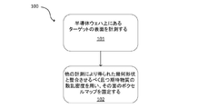
- ウェハ計量ツールを用い、半導体ウェハ上にあるターゲットの表面を計測し、更に
プロセッサを用いることで、幾何計測結果と整合させるべく且つ期待物質の散乱密度を用い前記表面のボクセルマップを固定する方法であり、固定済表面ボクセル全ての散乱密度の均一スケーリングが行われる方法。 - 請求項1に記載の方法であって、前記ウェハ計量ツールが限界寸法走査型電子顕微鏡である方法。
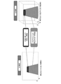
- 請求項1に記載の方法であり、前記ウェハ計量ツールが反射型小角X線スキャタロメータである方法であって、更に、反射モードに従い構成された計測ツールで以て前記ターゲットの表面を計測する方法。
- 請求項3に記載の方法であって、前記計測ツールが透過型小角X線スキャタロメータである方法。
- 請求項1に記載の方法であり、前記ウェハ計量ツールが光スキャタロメータである方法であって、更に、透過技術を用いるよう構成された計測ツールで以て前記ターゲットの表面を計測する方法。
- 請求項5に記載の方法であって、前記計測ツールが透過型小角X線スキャタロメータである方法。
- 請求項1に記載の方法であって、前記ターゲットの表面を計測する際に、そのターゲットの幾何形状を計測することで幾何計測結果を提供する方法。
- 請求項1に記載の方法であって、前記ターゲット内の物質に関連付けられている一組の値からボクセルへと散乱値を採取する方法。
- 請求項8に記載の方法であって、前記散乱値が連続的に浮動する方法。
- 半導体ウェハ上にあるターゲットの表面を計測するよう構成されたウェハ計量ツールと、
前記ウェハ計量ツールと電子通信するプロセッサと、
を備え、前記プロセッサが、幾何計測結果と整合させるべく且つ期待物質の散乱密度を用い、前記表面のボクセルマップを固定するよう構成されており、固定済表面ボクセル全ての散乱密度の均一スケーリングが行われるシステム。 - 請求項10に記載のシステムであって、前記ウェハ計量ツールが限界寸法走査型電子顕微鏡であるシステム。
- 請求項10に記載のシステムであり、前記ウェハ計量ツールが反射型小角X線スキャタロメータであるシステムであって、更に、反射モードを用いるよう構成されており前記プロセッサと電子通信する計測ツールを備えるシステム。
- 請求項12に記載のシステムであって、前記計測ツールが透過型小角X線スキャタロメータであるシステム。
- 請求項10に記載のシステムであり、前記ウェハ計量ツールが光スキャタロメータであるシステムであって、更に、透過技術を用いるよう構成されており前記プロセッサと電子通信する計測ツールを備えるシステム。
- 請求項14に記載のシステムであって、前記計測ツールが透過型小角X線スキャタロメータであるシステム。
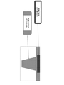
- 請求項10に記載のシステムであって、更に、透過技術を用いるよう構成されており前記プロセッサと電子通信する計測ツールを備え、前記ウェハ計量ツールが、更に、前記ターゲットの幾何形状を計測するよう構成されているシステム。
- 請求項16に記載のシステムであって、前記ウェハ計量ツールが反射型小角X線スキャタロメータ又は光スキャタロメータであり、前記計測ツールが透過型小角X線スキャタロメータであるシステム。
- 請求項16に記載のシステムであって、更に、前記ターゲット内の物質に関連付けられている複数個の散乱値を格納するよう構成された電子データ格納ユニットを備え、その電子データ格納ユニットが前記プロセッサと電子通信するシステム。
- 請求項18に記載のシステムであって、前記プロセッサが、前記ボクセルに関し前記一組の値から散乱値を採取するよう構成されているシステム。
- 請求項19に記載のシステムであって、前記散乱値が連続的に浮動するシステム。
Applications Claiming Priority (3)
| Application Number | Priority Date | Filing Date | Title |
|---|---|---|---|
| US16/047,818 US10677586B2 (en) | 2018-07-27 | 2018-07-27 | Phase revealing optical and X-ray semiconductor metrology |
| US16/047,818 | 2018-07-27 | ||
| PCT/US2019/043541 WO2020023810A1 (en) | 2018-07-27 | 2019-07-26 | Phase revealing optical and x-ray semiconductor metrology |
Publications (2)
| Publication Number | Publication Date |
|---|---|
| JP2021531663A true JP2021531663A (ja) | 2021-11-18 |
| JP7303868B2 JP7303868B2 (ja) | 2023-07-05 |
Family
ID=69182366
Family Applications (1)
| Application Number | Title | Priority Date | Filing Date |
|---|---|---|---|
| JP2021504446A Active JP7303868B2 (ja) | 2018-07-27 | 2019-07-26 | 位相解明光学及びx線半導体計量 |
Country Status (7)
| Country | Link |
|---|---|
| US (1) | US10677586B2 (ja) |
| JP (1) | JP7303868B2 (ja) |
| KR (1) | KR102518206B1 (ja) |
| CN (1) | CN112368812B (ja) |
| IL (1) | IL280009B2 (ja) |
| TW (1) | TWI780347B (ja) |
| WO (1) | WO2020023810A1 (ja) |
Families Citing this family (3)
| Publication number | Priority date | Publication date | Assignee | Title |
|---|---|---|---|---|
| US11610297B2 (en) * | 2019-12-02 | 2023-03-21 | Kla Corporation | Tomography based semiconductor measurements using simplified models |
| WO2021179290A1 (en) * | 2020-03-13 | 2021-09-16 | Yangtze Memory Technologies Co., Ltd. | Systems and methods for semiconductor chip hole geometry metrology |
| US12288668B2 (en) * | 2023-05-11 | 2025-04-29 | Applied Materials Israel Ltd. | Entropy based image processing for focused ion beam delayer-edge slices detection |
Citations (3)
| Publication number | Priority date | Publication date | Assignee | Title |
|---|---|---|---|---|
| JPH06160064A (ja) * | 1992-11-16 | 1994-06-07 | Mitsubishi Materials Shilicon Corp | 表面の検査方法および検査装置 |
| JP2002082063A (ja) * | 2000-09-05 | 2002-03-22 | Komatsu Electronic Metals Co Ltd | ウエハの表面検査装置及び検査方法 |
| JP2010025836A (ja) * | 2008-07-23 | 2010-02-04 | Hitachi High-Technologies Corp | 外観検査方法および外観検査装置、半導体検査装置ならびに半導体ウェハの断面検査装置 |
Family Cites Families (22)
| Publication number | Priority date | Publication date | Assignee | Title |
|---|---|---|---|---|
| US5608526A (en) | 1995-01-19 | 1997-03-04 | Tencor Instruments | Focused beam spectroscopic ellipsometry method and system |
| US5859424A (en) | 1997-04-08 | 1999-01-12 | Kla-Tencor Corporation | Apodizing filter system useful for reducing spot size in optical measurements and other applications |
| US6429943B1 (en) | 2000-03-29 | 2002-08-06 | Therma-Wave, Inc. | Critical dimension analysis with simultaneous multiple angle of incidence measurements |
| US7478019B2 (en) | 2005-01-26 | 2009-01-13 | Kla-Tencor Corporation | Multiple tool and structure analysis |
| US7567351B2 (en) | 2006-02-02 | 2009-07-28 | Kla-Tencor Corporation | High resolution monitoring of CD variations |
| CN101359611B (zh) * | 2007-07-30 | 2011-11-09 | 东京毅力科创株式会社 | 对光学计量系统的选定变量进行优化 |
| EP2748793B1 (en) | 2011-10-14 | 2017-10-11 | Ingrain, Inc. | Dual image method and system for generating a multi-dimensional image of a sample |
| WO2013158593A1 (en) * | 2012-04-18 | 2013-10-24 | Kla-Tencor Corporation | Critical dimension uniformity monitoring for extreme ultra-violet reticles |
| US10013518B2 (en) * | 2012-07-10 | 2018-07-03 | Kla-Tencor Corporation | Model building and analysis engine for combined X-ray and optical metrology |
| WO2014062972A1 (en) | 2012-10-18 | 2014-04-24 | Kla-Tencor Corporation | Symmetric target design in scatterometry overlay metrology |
| US9581430B2 (en) | 2012-10-19 | 2017-02-28 | Kla-Tencor Corporation | Phase characterization of targets |
| JP5974840B2 (ja) | 2012-11-07 | 2016-08-23 | ソニー株式会社 | シミュレーション方法、シミュレーションプログラム、シミュレータ、加工装置、半導体装置の製造方法 |
| US10769320B2 (en) | 2012-12-18 | 2020-09-08 | Kla-Tencor Corporation | Integrated use of model-based metrology and a process model |
| US9291554B2 (en) | 2013-02-05 | 2016-03-22 | Kla-Tencor Corporation | Method of electromagnetic modeling of finite structures and finite illumination for metrology and inspection |
| US10101670B2 (en) | 2013-03-27 | 2018-10-16 | Kla-Tencor Corporation | Statistical model-based metrology |
| US9915522B1 (en) | 2013-06-03 | 2018-03-13 | Kla-Tencor Corporation | Optimized spatial modeling for optical CD metrology |
| US9494535B2 (en) | 2014-04-21 | 2016-11-15 | Kla-Tencor Corporation | Scatterometry-based imaging and critical dimension metrology |
| US9874526B2 (en) | 2016-03-28 | 2018-01-23 | Kla-Tencor Corporation | Methods and apparatus for polarized wafer inspection |
| EP3240013B1 (en) * | 2016-04-26 | 2018-11-07 | FEI Company | Three-dimensional imaging in charged-particle microscopy |
| SG11201902745RA (en) * | 2016-10-17 | 2019-05-30 | Kla Tencor Corp | Optimizing training sets used for setting up inspection-related algorithms |
| US10775323B2 (en) * | 2016-10-18 | 2020-09-15 | Kla-Tencor Corporation | Full beam metrology for X-ray scatterometry systems |
| US10382699B2 (en) * | 2016-12-01 | 2019-08-13 | Varjo Technologies Oy | Imaging system and method of producing images for display apparatus |
-
2018
- 2018-07-27 US US16/047,818 patent/US10677586B2/en active Active
-
2019
- 2019-07-11 TW TW108124425A patent/TWI780347B/zh active
- 2019-07-26 WO PCT/US2019/043541 patent/WO2020023810A1/en not_active Ceased
- 2019-07-26 CN CN201980045267.3A patent/CN112368812B/zh active Active
- 2019-07-26 JP JP2021504446A patent/JP7303868B2/ja active Active
- 2019-07-26 KR KR1020217005462A patent/KR102518206B1/ko active Active
-
2021
- 2021-01-07 IL IL280009A patent/IL280009B2/en unknown
Patent Citations (3)
| Publication number | Priority date | Publication date | Assignee | Title |
|---|---|---|---|---|
| JPH06160064A (ja) * | 1992-11-16 | 1994-06-07 | Mitsubishi Materials Shilicon Corp | 表面の検査方法および検査装置 |
| JP2002082063A (ja) * | 2000-09-05 | 2002-03-22 | Komatsu Electronic Metals Co Ltd | ウエハの表面検査装置及び検査方法 |
| JP2010025836A (ja) * | 2008-07-23 | 2010-02-04 | Hitachi High-Technologies Corp | 外観検査方法および外観検査装置、半導体検査装置ならびに半導体ウェハの断面検査装置 |
Also Published As
| Publication number | Publication date |
|---|---|
| CN112368812A (zh) | 2021-02-12 |
| TW202007958A (zh) | 2020-02-16 |
| TWI780347B (zh) | 2022-10-11 |
| KR20210027497A (ko) | 2021-03-10 |
| KR102518206B1 (ko) | 2023-04-04 |
| CN112368812B (zh) | 2022-03-25 |
| IL280009A (en) | 2021-03-01 |
| IL280009B2 (en) | 2023-07-01 |
| US20200080836A1 (en) | 2020-03-12 |
| IL280009B1 (en) | 2023-03-01 |
| WO2020023810A1 (en) | 2020-01-30 |
| US10677586B2 (en) | 2020-06-09 |
| JP7303868B2 (ja) | 2023-07-05 |
Similar Documents
| Publication | Publication Date | Title |
|---|---|---|
| TWI760309B (zh) | 用於校正計量工具之系統、方法及計算機程式產品 | |
| KR102220435B1 (ko) | 웨이퍼에 걸친 파라미터 변동들에 기초한 측정 모델 최적화 | |
| CN111566674B (zh) | 通过先进机器学习技术的测量精确度的自动优化 | |
| CN104395996B (zh) | 基于光谱敏感度及工艺变化的测量配方优化 | |
| CN107408519B (zh) | 基于模型的单个参数测量的系统和方法 | |
| KR102245695B1 (ko) | 모델-기반 계측 및 프로세스 모델의 통합 사용 | |
| KR102055966B1 (ko) | 조합된 x-레이 및 광학 계측을 위한 모델 구축 및 분석 엔진, 방법, 그리고 컴퓨터 판독 가능한 매체 | |
| KR102046216B1 (ko) | 조합된 x선 및 광학적 계측 | |
| US10705434B2 (en) | Verification metrology target and their design | |
| KR101860042B1 (ko) | 메트롤로지 타겟의 디자인을 위한 장치 및 방법 | |
| KR20220107326A (ko) | 이미지 기반 및 산란측정 오버레이 측정을 위한 신호 응답 계측 | |
| CN104838251A (zh) | 用于具有优化系统参数的光学计量的设备及方法 | |
| CN106463430A (zh) | 用于测量半导体参数的设备、技术和目标设计 | |
| KR20200086746A (ko) | 진보된 나노 구조물들의 측정 방법론 | |
| CN114746991A (zh) | 使用简化模型的基于断层摄影术的半导体测量 | |
| US8875078B2 (en) | Reference library generation method for methods of inspection, inspection apparatus and lithographic apparatus | |
| US9347872B1 (en) | Meta-model based measurement refinement | |
| JP7303868B2 (ja) | 位相解明光学及びx線半導体計量 | |
| TWI667548B (zh) | 檢測方法與裝置及微影裝置 | |
| TW202536398A (zh) | 判定多層結構之光學性質之方法 |
Legal Events
| Date | Code | Title | Description |
|---|---|---|---|
| A621 | Written request for application examination |
Free format text: JAPANESE INTERMEDIATE CODE: A621 Effective date: 20220720 |
|
| A871 | Explanation of circumstances concerning accelerated examination |
Free format text: JAPANESE INTERMEDIATE CODE: A871 Effective date: 20220720 |
|
| A131 | Notification of reasons for refusal |
Free format text: JAPANESE INTERMEDIATE CODE: A131 Effective date: 20221025 |
|
| A521 | Request for written amendment filed |
Free format text: JAPANESE INTERMEDIATE CODE: A523 Effective date: 20230118 |
|
| A131 | Notification of reasons for refusal |
Free format text: JAPANESE INTERMEDIATE CODE: A131 Effective date: 20230307 |
|
| A521 | Request for written amendment filed |
Free format text: JAPANESE INTERMEDIATE CODE: A523 Effective date: 20230601 |
|
| TRDD | Decision of grant or rejection written | ||
| A01 | Written decision to grant a patent or to grant a registration (utility model) |
Free format text: JAPANESE INTERMEDIATE CODE: A01 Effective date: 20230613 |
|
| A61 | First payment of annual fees (during grant procedure) |
Free format text: JAPANESE INTERMEDIATE CODE: A61 Effective date: 20230623 |
|
| R150 | Certificate of patent or registration of utility model |
Ref document number: 7303868 Country of ref document: JP Free format text: JAPANESE INTERMEDIATE CODE: R150 |