JP2021531663A - Phase elucidation optics and X-ray semiconductor metric - Google Patents
Phase elucidation optics and X-ray semiconductor metric Download PDFInfo
- Publication number
- JP2021531663A JP2021531663A JP2021504446A JP2021504446A JP2021531663A JP 2021531663 A JP2021531663 A JP 2021531663A JP 2021504446 A JP2021504446 A JP 2021504446A JP 2021504446 A JP2021504446 A JP 2021504446A JP 2021531663 A JP2021531663 A JP 2021531663A
- Authority
- JP
- Japan
- Prior art keywords
- tool
- target
- wafer
- processor
- scattering
- Prior art date
- Legal status (The legal status is an assumption and is not a legal conclusion. Google has not performed a legal analysis and makes no representation as to the accuracy of the status listed.)
- Granted
Links
Images
Classifications
-
- G—PHYSICS
- G01—MEASURING; TESTING
- G01B—MEASURING LENGTH, THICKNESS OR SIMILAR LINEAR DIMENSIONS; MEASURING ANGLES; MEASURING AREAS; MEASURING IRREGULARITIES OF SURFACES OR CONTOURS
- G01B11/00—Measuring arrangements characterised by the use of optical techniques
- G01B11/24—Measuring arrangements characterised by the use of optical techniques for measuring contours or curvatures
-
- G—PHYSICS
- G01—MEASURING; TESTING
- G01B—MEASURING LENGTH, THICKNESS OR SIMILAR LINEAR DIMENSIONS; MEASURING ANGLES; MEASURING AREAS; MEASURING IRREGULARITIES OF SURFACES OR CONTOURS
- G01B11/00—Measuring arrangements characterised by the use of optical techniques
- G01B11/02—Measuring arrangements characterised by the use of optical techniques for measuring length, width or thickness
- G01B11/06—Measuring arrangements characterised by the use of optical techniques for measuring length, width or thickness for measuring thickness ; e.g. of sheet material
- G01B11/0616—Measuring arrangements characterised by the use of optical techniques for measuring length, width or thickness for measuring thickness ; e.g. of sheet material of coating
- G01B11/0641—Measuring arrangements characterised by the use of optical techniques for measuring length, width or thickness for measuring thickness ; e.g. of sheet material of coating with measurement of polarization
-
- G—PHYSICS
- G01—MEASURING; TESTING
- G01B—MEASURING LENGTH, THICKNESS OR SIMILAR LINEAR DIMENSIONS; MEASURING ANGLES; MEASURING AREAS; MEASURING IRREGULARITIES OF SURFACES OR CONTOURS
- G01B15/00—Measuring arrangements characterised by the use of electromagnetic waves or particle radiation, e.g. by the use of microwaves, X-rays, gamma rays or electrons
- G01B15/04—Measuring arrangements characterised by the use of electromagnetic waves or particle radiation, e.g. by the use of microwaves, X-rays, gamma rays or electrons for measuring contours or curvatures
-
- G—PHYSICS
- G01—MEASURING; TESTING
- G01N—INVESTIGATING OR ANALYSING MATERIALS BY DETERMINING THEIR CHEMICAL OR PHYSICAL PROPERTIES
- G01N21/00—Investigating or analysing materials by the use of optical means, i.e. using sub-millimetre waves, infrared, visible or ultraviolet light
- G01N21/17—Systems in which incident light is modified in accordance with the properties of the material investigated
- G01N21/47—Scattering, i.e. diffuse reflection
-
- G—PHYSICS
- G01—MEASURING; TESTING
- G01N—INVESTIGATING OR ANALYSING MATERIALS BY DETERMINING THEIR CHEMICAL OR PHYSICAL PROPERTIES
- G01N21/00—Investigating or analysing materials by the use of optical means, i.e. using sub-millimetre waves, infrared, visible or ultraviolet light
- G01N21/84—Systems specially adapted for particular applications
- G01N21/88—Investigating the presence of flaws or contamination
- G01N21/95—Investigating the presence of flaws or contamination characterised by the material or shape of the object to be examined
- G01N21/9501—Semiconductor wafers
- G01N21/9503—Wafer edge inspection
-
- G—PHYSICS
- G01—MEASURING; TESTING
- G01N—INVESTIGATING OR ANALYSING MATERIALS BY DETERMINING THEIR CHEMICAL OR PHYSICAL PROPERTIES
- G01N23/00—Investigating or analysing materials by the use of wave or particle radiation, e.g. X-rays or neutrons, not covered by groups G01N3/00 – G01N17/00, G01N21/00 or G01N22/00
- G01N23/02—Investigating or analysing materials by the use of wave or particle radiation, e.g. X-rays or neutrons, not covered by groups G01N3/00 – G01N17/00, G01N21/00 or G01N22/00 by transmitting the radiation through the material
- G01N23/06—Investigating or analysing materials by the use of wave or particle radiation, e.g. X-rays or neutrons, not covered by groups G01N3/00 – G01N17/00, G01N21/00 or G01N22/00 by transmitting the radiation through the material and measuring the absorption
- G01N23/083—Investigating or analysing materials by the use of wave or particle radiation, e.g. X-rays or neutrons, not covered by groups G01N3/00 – G01N17/00, G01N21/00 or G01N22/00 by transmitting the radiation through the material and measuring the absorption the radiation being X-rays
-
- G—PHYSICS
- G01—MEASURING; TESTING
- G01N—INVESTIGATING OR ANALYSING MATERIALS BY DETERMINING THEIR CHEMICAL OR PHYSICAL PROPERTIES
- G01N23/00—Investigating or analysing materials by the use of wave or particle radiation, e.g. X-rays or neutrons, not covered by groups G01N3/00 – G01N17/00, G01N21/00 or G01N22/00
- G01N23/20—Investigating or analysing materials by the use of wave or particle radiation, e.g. X-rays or neutrons, not covered by groups G01N3/00 – G01N17/00, G01N21/00 or G01N22/00 by using diffraction of the radiation by the materials, e.g. for investigating crystal structure; by using scattering of the radiation by the materials, e.g. for investigating non-crystalline materials; by using reflection of the radiation by the materials
- G01N23/201—Investigating or analysing materials by the use of wave or particle radiation, e.g. X-rays or neutrons, not covered by groups G01N3/00 – G01N17/00, G01N21/00 or G01N22/00 by using diffraction of the radiation by the materials, e.g. for investigating crystal structure; by using scattering of the radiation by the materials, e.g. for investigating non-crystalline materials; by using reflection of the radiation by the materials by measuring small-angle scattering
-
- G—PHYSICS
- G01—MEASURING; TESTING
- G01N—INVESTIGATING OR ANALYSING MATERIALS BY DETERMINING THEIR CHEMICAL OR PHYSICAL PROPERTIES
- G01N23/00—Investigating or analysing materials by the use of wave or particle radiation, e.g. X-rays or neutrons, not covered by groups G01N3/00 – G01N17/00, G01N21/00 or G01N22/00
- G01N23/22—Investigating or analysing materials by the use of wave or particle radiation, e.g. X-rays or neutrons, not covered by groups G01N3/00 – G01N17/00, G01N21/00 or G01N22/00 by measuring secondary emission from the material
- G01N23/225—Investigating or analysing materials by the use of wave or particle radiation, e.g. X-rays or neutrons, not covered by groups G01N3/00 – G01N17/00, G01N21/00 or G01N22/00 by measuring secondary emission from the material using electron or ion
- G01N23/2251—Investigating or analysing materials by the use of wave or particle radiation, e.g. X-rays or neutrons, not covered by groups G01N3/00 – G01N17/00, G01N21/00 or G01N22/00 by measuring secondary emission from the material using electron or ion using incident electron beams, e.g. scanning electron microscopy [SEM]
-
- G—PHYSICS
- G06—COMPUTING OR CALCULATING; COUNTING
- G06T—IMAGE DATA PROCESSING OR GENERATION, IN GENERAL
- G06T9/00—Image coding
- G06T9/20—Contour coding, e.g. using detection of edges
-
- H10P72/06—
-
- H10P74/203—
-
- H10P74/238—
-
- H10P74/27—
-
- G—PHYSICS
- G01—MEASURING; TESTING
- G01B—MEASURING LENGTH, THICKNESS OR SIMILAR LINEAR DIMENSIONS; MEASURING ANGLES; MEASURING AREAS; MEASURING IRREGULARITIES OF SURFACES OR CONTOURS
- G01B2210/00—Aspects not specifically covered by any group under G01B, e.g. of wheel alignment, caliper-like sensors
- G01B2210/56—Measuring geometric parameters of semiconductor structures, e.g. profile, critical dimensions or trench depth
-
- G—PHYSICS
- G01—MEASURING; TESTING
- G01N—INVESTIGATING OR ANALYSING MATERIALS BY DETERMINING THEIR CHEMICAL OR PHYSICAL PROPERTIES
- G01N2223/00—Investigating materials by wave or particle radiation
- G01N2223/10—Different kinds of radiation or particles
- G01N2223/101—Different kinds of radiation or particles electromagnetic radiation
- G01N2223/1016—X-ray
-
- G—PHYSICS
- G01—MEASURING; TESTING
- G01N—INVESTIGATING OR ANALYSING MATERIALS BY DETERMINING THEIR CHEMICAL OR PHYSICAL PROPERTIES
- G01N2223/00—Investigating materials by wave or particle radiation
- G01N2223/60—Specific applications or type of materials
- G01N2223/611—Specific applications or type of materials patterned objects; electronic devices
- G01N2223/6116—Specific applications or type of materials patterned objects; electronic devices semiconductor wafer
-
- H—ELECTRICITY
- H01—ELECTRIC ELEMENTS
- H01J—ELECTRIC DISCHARGE TUBES OR DISCHARGE LAMPS
- H01J2237/00—Discharge tubes exposing object to beam, e.g. for analysis treatment, etching, imaging
- H01J2237/22—Treatment of data
-
- H—ELECTRICITY
- H01—ELECTRIC ELEMENTS
- H01J—ELECTRIC DISCHARGE TUBES OR DISCHARGE LAMPS
- H01J2237/00—Discharge tubes exposing object to beam, e.g. for analysis treatment, etching, imaging
- H01J2237/26—Electron or ion microscopes
- H01J2237/28—Scanning microscopes
- H01J2237/2813—Scanning microscopes characterised by the application
- H01J2237/2814—Measurement of surface topography
Landscapes
- Physics & Mathematics (AREA)
- General Physics & Mathematics (AREA)
- Health & Medical Sciences (AREA)
- Chemical & Material Sciences (AREA)
- Biochemistry (AREA)
- Analytical Chemistry (AREA)
- General Health & Medical Sciences (AREA)
- Immunology (AREA)
- Pathology (AREA)
- Life Sciences & Earth Sciences (AREA)
- Engineering & Computer Science (AREA)
- Multimedia (AREA)
- Toxicology (AREA)
- Theoretical Computer Science (AREA)
- Electromagnetism (AREA)
- Crystallography & Structural Chemistry (AREA)
- Manufacturing & Machinery (AREA)
- Testing Or Measuring Of Semiconductors Or The Like (AREA)
- Computer Hardware Design (AREA)
- Microelectronics & Electronic Packaging (AREA)
- Power Engineering (AREA)
- Length Measuring Devices With Unspecified Measuring Means (AREA)
- Exposure And Positioning Against Photoresist Photosensitive Materials (AREA)
- Analysing Materials By The Use Of Radiation (AREA)
- Condensed Matter Physics & Semiconductors (AREA)
- Investigating Or Analysing Materials By The Use Of Chemical Reactions (AREA)
- Materials For Photolithography (AREA)
Abstract
本願開示の諸実施形態によれば、半導体ウェハ上にあるターゲットを再構築及び/又は撮像することが可能となる。半導体ウェハ上にあるターゲットの表面を、ウェハ計量ツールを用いて計測する。その面のボクセルマップを、幾何計測結果と整合させるべく且つ期待物質の散乱密度を用い固定する。固定済表面ボクセル全ての散乱密度の均一スケーリングが行われうる。 According to the embodiments disclosed in the present application, it is possible to reconstruct and / or image a target on a semiconductor wafer. The surface of the target on the semiconductor wafer is measured using a wafer weighing tool. The voxel map of the surface is fixed using the scattering density of the expected material in order to match the geometric measurement result. Uniform scaling of the scattering densities of all fixed surface voxels can be done.
Description
本件開示は半導体計量に関する。 This disclosure relates to semiconductor weighing.
半導体製造業の発展により、かつてなく強い要求が歩留まり管理に、またとりわけ計量及び検査システムに課されつつある。限界寸法が小さくなり続けている。高歩留まり高付加価値生産達成所要時間を縮めよと、市場が業界を駆り立てている。歩留まり問題を察知してからそれを正すまでの合計時間を縮めることが、半導体製造業者にとり投資収益率の決め手となっている。 With the development of the semiconductor manufacturing industry, unprecedented demands are being placed on yield management, and especially on weighing and inspection systems. The marginal dimensions continue to shrink. The market is driving the industry to reduce the time required to achieve high yield and high value-added production. Shortening the total time from detecting a yield problem to correcting it is the decisive factor for the return on investment for semiconductor manufacturers.
半導体デバイス例えば論理デバイス及び記憶デバイスを作成する際には、通常、多数の作成プロセスを用い半導体ウェハを処理することで、それら半導体デバイスの様々なフィーチャ(外形特徴)及び複数個の階層が形成される。例えばリソグラフィなる半導体製造プロセスでは、半導体ウェハ上に配置されたフォトレジストへと、レティクルからパターンが転写される。半導体製造プロセスの別例には、これに限られるものではないが化学機械研磨(CMP)、エッチング、堆積及びイオンインプランテーションがある。複数個の半導体デバイスを1枚の半導体ウェハ上に配列をなし作成した後、個別の半導体デバイスへと分けるようにするとよい。 When manufacturing semiconductor devices such as logic devices and storage devices, processing semiconductor wafers using a large number of manufacturing processes usually forms various features (external features) and a plurality of layers of the semiconductor devices. NS. For example, in a semiconductor manufacturing process called lithography, a pattern is transferred from a reticle to a photoresist arranged on a semiconductor wafer. Other examples of semiconductor manufacturing processes include, but are not limited to, chemical mechanical polishing (CMP), etching, deposition and ion implantation. It is preferable to arrange a plurality of semiconductor devices on one semiconductor wafer and then divide them into individual semiconductor devices.
計量プロセスは、半導体製造プロセス中の様々な工程で、そのプロセスを監視、制御すべく用いられている。計量プロセスが検査プロセスと異なる点は、ウェハ上の欠陥が検出される検査プロセスと違い、それらウェハに備わる一通り又は複数通りの特性であり既存検査ツールを用いても判別できないものを、計量プロセスを用いれば計測できる点にある。計量プロセスを用いウェハの特性一通り又は複数通りを計測することで、当該一通り又は複数通りの特性からプロセスの性能を判別することが可能となる。例えば、そのプロセス中にそれらウェハ上に形成されたフィーチャの寸法(例.ライン幅、厚み等々)を、計量プロセスにて計測することができる。加えて、それらウェハの特性一通り又は複数通りが(例.その特性(群)向けの所定範囲外にあり)許容不能なものであっても、それらウェハの特性一通り又は複数通りについての計測結果を用いそのプロセスのパラメタ1個又は複数個を改変することで、そのプロセスにより製造される後続ウェハの特性を許容可能なものとすることができる。 Weighing processes are used in various processes during the semiconductor manufacturing process to monitor and control the process. The difference between the weighing process and the inspection process is that, unlike the inspection process in which defects on the wafer are detected, the weighing process has one or more characteristics that cannot be identified even by using existing inspection tools. It is a point that can be measured by using. By measuring one or more characteristics of the wafer using the weighing process, it is possible to determine the performance of the process from the one or more characteristics. For example, the dimensions of features formed on those wafers during the process (eg, line width, thickness, etc.) can be measured in the weighing process. In addition, even if one or more of the characteristics of those wafers are unacceptable (eg, outside the predetermined range for that characteristic (group)), a measurement of one or more of the characteristics of those wafers. By modifying one or more parameters of the process using the results, the characteristics of subsequent wafers manufactured by the process can be made acceptable.
半導体計量トモグラフィでは、周期性平面ターゲットに発する回折光からフリーフォームの散乱密度マップ(SDM)が決定される。硬X線では散乱密度が複素数となり、1なる屈折率からの偏差たる実部と、消衰係数たる虚部とがそれにより表される。X線波長の二乗を2πにより除したものを古典電子半径に乗じたものが関わる定数逆スケーリングを行うと、そのSDMの実部がその物質の電子密度と等価なものになる。そのため、電子密度なる語が、散乱密度に代わる代用定義として用いられることが多い。密度決定は、そのSDMを正規化しつつ模擬回折パターンと計測回折パターンとを整合させる最適化プロセスの成果である。SDMは、X線ターゲットの散乱ボリュームを埋め尽くす体積要素(ボクセル)に割り当てられた一組の散乱密度なる形態を採るものであり、そのX線ターゲットは、平面方向(x,y)にて通常は周期的な単位セルをなし且つそれに対し垂直な方向(z)にて通常は非周期的な散乱領域をなしている。この散乱ボリュームのことを拡張単位セルという。 In semiconductor metric tomography, the freeform scattering density map (SDM) is determined from the diffracted light emitted to the periodic plane target. In hard X-rays, the scattering density becomes a complex number, and the real part, which is a deviation from the refractive index of 1, and the imaginary part, which is an extinction coefficient, are represented by it. When constant inverse scaling involving the square of the X-ray wavelength divided by 2π multiplied by the classical electron radius is performed, the real part of the SDM becomes equivalent to the electron density of the material. Therefore, the term electron density is often used as an alternative definition to scattering density. Density determination is the result of an optimization process that matches the simulated diffraction pattern with the measured diffraction pattern while normalizing the SDM. The SDM takes the form of a set of scattering densities assigned to a volume element (voxel) that fills the scattering volume of the X-ray target, and the X-ray target is usually in the plane direction (x, y). Has a periodic unit cell and usually has an aperiodic scattering region in the direction (z) perpendicular to it. This scattered volume is called an extended unit cell.
回折光強度からSDMを推し量ろうとする技術の短所の一つは、計測にて入手できる絶対又は相対位相情報がないことである。そのため、SDMを一意に決定する機構が存在していない。実のところ、全く同じ回折光信号を生成できるSDMには数多くの例がある。更に、散乱ボリュームの所在個所に対する高さ依存性が硬X線スペクトルでは弱い。これが原因となり、決定されるSDMにて幾種類かの曖昧性、例えば並進、空間フラクション及び垂直方向反転曖昧性が生じる。並進方向曖昧性があると、SDMをどの方向にシフトさせても模擬計測結果に変化がないことがあるため、制約条件上の効果が全くない。空間フラクション曖昧性があると、単純構造内の個別な二通りの幾何形状によって、0次以外の全次数に関し同じ散乱プロファイルがもたらされうる。垂直方向反転曖昧性があると、水平面を基準としてそのSDMをひっくり返したとしても、その単一の散乱モデルにより同じ模擬スペクトルがもたらされる。 One of the disadvantages of the technique of trying to estimate SDM from diffracted light intensity is the lack of absolute or relative phase information available by measurement. Therefore, there is no mechanism for uniquely determining SDM. In fact, there are many examples of SDMs that can generate exactly the same diffracted light signal. Furthermore, the height dependence of the scattered volume on the location is weak in the hard X-ray spectrum. This causes some ambiguity in the determined SDM, such as translation, spatial fraction and vertical inversion ambiguity. If there is ambiguity in the translational direction, there may be no change in the simulated measurement result regardless of the direction in which the SDM is shifted, so that there is no effect on the constraint conditions. With spatial fraction ambiguity, two separate geometries within a simple structure can result in the same scattering profile for all non-zero orders. With vertical inversion ambiguity, the single scattering model yields the same simulated spectrum, even if the SDM is flipped over with respect to the horizontal plane.
従前の諸技術では、ある意味で、SDM初期条件から位相を借用すること及び/又は決定SDM・初期SDM間最適化差にペナルティを課すことによって、位相欠如を解決しようと試みられていた。しかしながら、初期条件から位相を誘導すると、推定されるSDMがその初期SDM寄りに歪むことがある。これにより、そこには存在しないはずの特徴又はそこに存在すべき幾何学的特徴を抑圧する特徴が、その推定SDM内にもたらされることがある。 Previous techniques have, in a sense, attempted to solve the phase deficiency by borrowing the phase from the SDM initial conditions and / or imposing a penalty on the optimization difference between the determined SDM and the initial SDM. However, when the phase is derived from the initial conditions, the estimated SDM may be distorted toward the initial SDM. This may result in features within the estimated SDM that suppress features that should not be there or geometric features that should be there.
そのため、計量における改良が必要とされている。 Therefore, improvements in weighing are needed.
第1実施形態では方法を提供する。本方法では、ウェハ計量ツールを用い、半導体ウェハ上にあるターゲットの表面を計測する。プロセッサを用いることで、幾何計測結果と整合させるべく且つ期待物質の散乱密度を用いその面のボクセルマップを固定する。それら固定済表面ボクセル全ての散乱密度の均一スケーリングが行われる。 The first embodiment provides a method. In this method, a wafer weighing tool is used to measure the surface of a target on a semiconductor wafer. By using a processor, the voxel map of the surface is fixed by using the scattering density of the expected material in order to match the geometric measurement result. Uniform scaling of the scattering densities of all those fixed surface voxels is performed.
ある例では、前記ウェハ計量ツールが限界寸法走査型電子顕微鏡とされる。 In one example, the wafer weighing tool is a limit dimension scanning electron microscope.
別の例では前記ウェハ計量ツールが反射型小角X線スキャタロメータ(散乱計)とされる。本方法では、反射モードに従い構成された計測ツールで以て前記ターゲットの表面を計測することができる。その計測ツールたりうるものには透過型小角X線スキャタロメータがある。 In another example, the wafer weighing tool is a reflective small-angle X-ray scatterometer. In this method, the surface of the target can be measured by a measuring tool configured according to the reflection mode. There is a transmissive small-angle X-ray scatterometer as a measurement tool.
別の例では前記ウェハ計量ツールが光スキャタロメータとされる。本方法では、透過技術を用いるよう構成された計測ツールで以てターゲット表面を計測することができる。その計測ツールたりうるものには透過型小角X線スキャタロメータがある。 In another example, the wafer weighing tool is an optical scatterometer. In this method, the target surface can be measured with a measuring tool configured to use permeation technology. There is a transmissive small-angle X-ray scatterometer as a measurement tool.
前記ターゲット表面を計測する際に、そのターゲットの幾何形状を計測することで幾何計測結果を提供することができる。 When measuring the surface of the target, the geometric measurement result can be provided by measuring the geometric shape of the target.
ボクセル向けの散乱値は、ターゲット内物質に関連付けられた一組の値から採取することができる。それら散乱値は連続的に浮動しうる。 Scattering values for voxels can be taken from a set of values associated with the substance in the target. Those scattered values can float continuously.
第2実施形態ではシステムを提供する。本システムは、半導体ウェハ上にあるターゲットの表面を計測するよう構成されたウェハ計量ツールと、そのウェハ計量ツールと電子通信するプロセッサとを有する。そのプロセッサを、幾何計測結果と整合させるべく且つ期待物質の散乱密度を用い前記表面のボクセルマップを固定するよう、構成する。それら固定済表面ボクセル全ての散乱密度の均一スケーリングが行われる。 The second embodiment provides a system. The system includes a wafer weighing tool configured to measure the surface of a target on a semiconductor wafer and a processor that electronically communicates with the wafer weighing tool. The processor is configured to fix the voxel map on the surface in order to match the geometric measurement results and to use the scattering density of the expected material. Uniform scaling of the scattering densities of all those fixed surface voxels is performed.
ある例では前記ウェハ計量ツールが限界寸法走査型電子顕微鏡とされる。 In one example, the wafer weighing tool is a limit dimension scanning electron microscope.
別の例では前記ウェハ計量ツールが反射型小角X線スキャタロメータとされる。本システムには、反射モードを用いるよう構成されており前記プロセッサと電子通信する計測ツールを設けることができる。その計測ツールたりうるものには透過型小角X線スキャタロメータがある。 In another example, the wafer weighing tool is a reflective small-angle X-ray scatterometer. The system is configured to use a reflection mode and can be provided with a measurement tool that electronically communicates with the processor. There is a transmissive small-angle X-ray scatterometer as a measurement tool.
別の例では前記ウェハ計量ツールが光スキャタロメータとされる。本システムには、透過技術を用いるよう構成されており前記プロセッサと電子通信する計測ツールを設けることができる。その計測ツールたりうるものには透過型小角X線スキャタロメータがある。 In another example, the wafer weighing tool is an optical scatterometer. The system is configured to use transmission technology and can be provided with a measurement tool that electronically communicates with the processor. There is a transmissive small-angle X-ray scatterometer as a measurement tool.
本システムには、透過技術を用いるよう構成されており前記プロセッサと電子通信する計測ツールを設けることができる。前記ウェハ計量ツールを、更に、前記ターゲットの幾何形状を計測するよう構成することができる。ある例ではそのウェハ計量ツールが反射型小角X線スキャタロメータ又は光スキャタロメータとされ、その計測ツールが透過型小角X線スキャタロメータとされる。本システムには、ターゲット内物質に関連付けられている複数個の散乱値を格納するよう構成された、電子データ格納ユニットを設けることができる。その電子データ格納ユニットを前記プロセッサと電子通信させてもよい。そのプロセッサを、前記一組の値からボクセル向けに散乱値を採取するよう構成することができる。それら散乱値は連続的に浮動しうる。 The system is configured to use transmission technology and can be provided with a measurement tool that electronically communicates with the processor. The wafer weighing tool can be further configured to measure the geometry of the target. In one example, the wafer weighing tool is a reflective small-angle X-ray scatterometer or an optical scatterometer, and the measuring tool is a transmissive small-angle X-ray scatterometer. The system may be provided with an electronic data storage unit configured to store a plurality of scattering values associated with the substance in the target. The electronic data storage unit may be electronically communicated with the processor. The processor can be configured to collect scatter values for voxels from the set of values. Those scattered values can float continuously.
本件開示の性質及び目的についてのより遺漏なき理解のためには、後掲の詳細記述と併せ、以下の添付図面を参照すべきである。 For a more complete understanding of the nature and purpose of the Disclosure, the following attached drawings should be referred to along with the detailed description below.
特定の諸実施形態により特許請求の範囲記載の主題につき記述するが、本件開示の技術的範囲内には、本願中で説明される諸利益及び諸特徴の部分集合しか提供されない諸実施形態を含め、他の諸実施形態も存在している。本件開示の技術的範囲から離隔することなく様々な構造的、論理的、処理ステップ的及び電子的変更を施すことができる。従って、本件開示の技術的範囲は専ら別項の特許請求の範囲への参照によって定まる。 Although the subject matter of the claims is described by specific embodiments, the technical scope of the present disclosure includes embodiments that provide only a subset of the benefits and features described herein. , Other embodiments also exist. Various structural, logical, processing step and electronic changes can be made without departing from the technical scope of the present disclosure. Therefore, the technical scope of the present disclosure is determined solely by reference to the claims in another paragraph.
本願開示の諸実施形態では二種類の位相回復又は部分回復を物語っている。一種類目は撮像法由来のものであり、物体の一部分につき計測することができる。そしてその計測結果を用いることで、初期条件を補正することや、その最適化に対する付加的ペナルティ条件を提供することができる。二種類目はスキャタロメトリ(散乱計測)法を用いるものであり、計測された付加的スペクトルに含まれる付加的な情報が、少なくとも垂直方向曖昧性を解決するのに役立つ。これら二種類の位相回復又は部分回復を併用することで、ある種の構造に関し秀逸な結果を提供することができる。本願開示の諸実施形態によれば、透過型小角X線散乱(T−SAXS)スキャタロメトリ単独時よりも効率的に、ターゲットを再構築及び/又は撮像することが可能となりうる。本願記載の情報処理方法の諸実施形態によれば、トモグラフィに係る結果が得られるまでの時間を短縮することもできる。 The embodiments disclosed in the present application represent two types of phase retrieval or partial retrieval. The first type is derived from the imaging method and can measure a part of an object. Then, by using the measurement result, it is possible to correct the initial condition and provide an additional penalty condition for the optimization. The second type uses the scatterometry method, where the additional information contained in the measured additional spectrum helps to at least resolve the vertical ambiguity. The combination of these two types of phase retrieval or partial retrieval can provide excellent results for certain structures. According to the embodiments disclosed in the present application, it may be possible to reconstruct and / or image the target more efficiently than when the transmitted small-angle X-ray scattering (T-SAXS) scatterometry alone is used. According to the various embodiments of the information processing method described in the present application, it is possible to shorten the time until the result related to tomography is obtained.
本願記載の如く位相回復を用いることで、SDMの一部分が決定された後に、そのSDMの残余未知部分に係る一意解を、計測信号から得ることができる。記載されている諸方法では拡張単位セルのSDMマップの頂層が精巧に作成される。他の諸実施形態ではそのSDMの他部分が決定される。 By using phase retrieval as described in the present application, after a part of the SDM is determined, a unique solution relating to the residual unknown part of the SDM can be obtained from the measurement signal. The methods described elaborately create the top layer of the SDM map of the extended unit cell. In other embodiments, other parts of the SDM are determined.
SDMのうち何れかの部分を固定しても、そのSDMについての一意解が計測回折信号のみから得られることは、必ずしも保証されない。とはいえ、十分な個数の計測コンフィギュレーションが与えられ、十分な量の散乱がそのSDMの固定部分から与えられれば、一意解を得ることができる。 Even if any part of the SDM is fixed, it is not always guaranteed that a unique solution for the SDM can be obtained only from the measured diffraction signal. Nonetheless, a unique solution can be obtained given a sufficient number of measurement configurations and a sufficient amount of scatter from a fixed portion of the SDM.
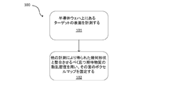
図1は方法100のフローチャートである。方法100を用いることで、ターゲット頂層のSDMを割り当てることができ、その頂層より下のSDMを決定することができる。101では、半導体ウェハ上にあるターゲットの表面が、ウェハ計量ツールを用い計測される。ウェハ計量ツールの例としては、限界寸法走査型電子顕微鏡(CD−SEM)、反射型小角X線スキャタロメータ、光スキャタロメータ等がある。
FIG. 1 is a flowchart of the
ターゲット頂表面の幾何形状を計測により判別した後は、ターゲット表面に存在するものと期待される諸物質の散乱密度を用い、それら計測された幾何形状に基づき、諸ボクセルの頂層のSDMが割り当てられる。入射輻射束が散乱計算にて独立に算入されない場合は、それら固定済表面ボクセル全ての散乱密度の均一スケーリングを用い、その輻射束における不確定性を算入すればよい。例えば102では、その表面のボクセルマップが、他の計測により求まった幾何形状と整合させるべく且つ期待物質の散乱密度を用い固定される。固定済表面ボクセル全ての散乱密度の均一スケーリングが行われうる。例えば、固定済表面ボクセル全ての散乱密度の均一スケーリングのみが行われうるし、固定済表面ボクセル全ての散乱密度の少なくとも幾ばくか均一なスケーリングが行われうる。 After determining the geometry of the top surface of the target by measurement, the scattering densities of the substances expected to be present on the surface of the target are used, and the SDM of the top layer of the voxels is assigned based on the measured geometry. .. If the incident radiation flux is not included independently in the scattering calculation, uniform scaling of the scattering densities of all those fixed surface voxels may be used to include the uncertainty in the radiation flux. For example, in 102, the voxel map on the surface is fixed to match the geometry obtained by other measurements and using the scattering density of the expected material. Uniform scaling of the scattering densities of all fixed surface voxels can be done. For example, only uniform scaling of the scattering densities of all fixed surface voxels can be done, or at least some uniform scaling of the scattering densities of all fixed surface voxels can be done.
一般に、入射束にも物質の散乱密度にも不確定性があるため、それを固定値に設定するのが難しいことがある。ある例ではその代わりにスケーリング因子が適用される。その表面内に複数の物質が存するのであれば、物質毎に別々のスケーリング因子にする必要があろう。 In general, it can be difficult to set a fixed value because of the uncertainty in both the incident flux and the scattering density of the material. In some cases scaling factors are applied instead. If there are multiple substances on the surface, it will be necessary to use different scaling factors for each substance.
ボクセルは小さくて規則的な塊(ボリューム)であり、直角プリズム状であることが多い。ボクセルの幾何形状は、拡張単位セルの埋め尽くし、即ちそれらボリュームの有限集合によりその拡張単位セルを重複なしで完全に覆うことを、許すものとする。一例としては、レンダリングシステムにて、ボクセルの位置を、他の諸ボクセルに対する自ボクセルの位置(即ちある単一のボリュメトリック画像を組成するデータ構造における自ボクセルの位置)に基づき推定することができる。ボクセルにより、規則的に標本化された空間であり非ホモジニアスに満たされたものを、表すことができる。 Voxels are small, regular lumps (volumes), often in the shape of right-angled prisms. The geometry of voxels allows the expansion unit cells to be filled, i.e., to completely cover the expansion unit cells with a finite set of their volumes without duplication. As an example, in a rendering system, the position of a voxel can be estimated based on the position of the voxel with respect to other voxels (that is, the position of the voxel in the data structure constituting a single volumetric image). .. Voxels can represent regularly sampled spaces that are non-homogeneously filled.
諸ボクセルには、ターゲット内物質に関連付けられている一組の値から散乱値、例えば物質の散乱又は電子密度を含むそれを採取することができる。本願記載の計量方式ではそれら散乱値が連続的に変化しうるので、下はボクセルの離散化レベルに至るまで、ターゲット内形状をレンダリングすることができる。このレンダリングはX線画像のそれに類似しており、各図画構成要素(画素)の輝度が、点状光源から放射されるX線の円錐に対する、ターゲット物質の透過率に比例する。 Voxels can be harvested from a set of values associated with a substance within a target, including the scattering value, eg, the scattering or electron density of the substance. Since the scattering values can change continuously in the measurement method described in the present application, the shape in the target can be rendered down to the discretization level of voxels below. This rendering is similar to that of an X-ray image, where the brightness of each drawing component (pixel) is proportional to the transmission of the target material to the X-ray cone emitted by the point light source.
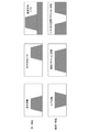
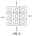
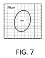
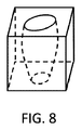
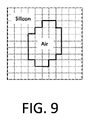
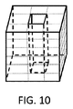
図6〜図10は方法100の一例である。図6はシリコンにおける孔の2D周期アレイ例である。図7は計測又は撮像された表面の例であり、ボクセル化用格子線が重畳されている。図7は図6に対応させうる。図8はその2D周期アレイ内の単位セル1個の3D外観例である。図9は計測又は撮像されボクセル化された表面の例であり、ボクセル化エッジが格子線に対し整列している。図9は図8に対応させうる。図10は粗ボクセル化後の2D周期アレイ内の単位セル1個の3D外観例である。図10には3×3×6ボクセルアレイが示されている。9個のボクセルからなる頂層が補助計測により決定され、その残りをX線散乱トモグラフィ法により一意に決定することができる。
6 to 10 are examples of the
ある実施形態によれば、反射技術を用いるよう構成された計測ツール、とりわけターゲットへの浸透深さが比較的小さな類のシステムで以て、ターゲット表面を計測することができる。その計測ツールを別のウェハ計量ツール或いは他の何らかの計測システムにしてもよい。ある例によれば、そのウェハ計量ツールを反射型X線スキャタロメータとすることができ、且つ計測ツールを透過型小角X線スキャタロメータとすることができる。別例によれば、そのウェハ計量ツールを光スキャタロメータとし、計測ツールを透過型小角X線スキャタロメータとすることができる。これらのツールを、単独で又はタンデムにて用いることで、それら計量ツールにより指し示される幾何に対しターゲットの表面を固定することができ、その残りは、それら固定済表面ボクセル全ての散乱密度の均一スケーリングとすることができる。 According to one embodiment, a measurement tool configured to use reflection techniques, especially a system with a relatively small penetration depth into the target, can be used to measure the surface of the target. The measurement tool may be another wafer weighing tool or some other measurement system. According to one example, the wafer weighing tool can be a reflective X-ray scatterometer, and the measuring tool can be a transmissive small-angle X-ray scatterometer. According to another example, the wafer weighing tool can be an optical scatterometer, and the measuring tool can be a transmissive small-angle X-ray scatterometer. Using these tools alone or in tandem, the surface of the target can be fixed to the geometry pointed to by those weighing tools, the rest of which is the uniform scattering density of all those fixed surface voxels. It can be scaling.
ハイブリッド撮像実施形態では、撮像法例えばCD−SEM撮像又はコヒーレント回折撮像によりターゲット表面の計測を行うことができる。その画像を用いることで、期待物質の散乱密度を用い、表面のボクセルマップをその撮像結果の幾何に対し固定することができ、その残りは、それら固定済表面ボクセル全ての散乱密度の均一スケーリングとすることができる。 In the hybrid imaging embodiment, the target surface can be measured by an imaging method such as CD-SEM imaging or coherent diffraction imaging. By using the image, the scattering density of the expected material can be used to fix the surface voxel map to the geometry of the imaged result, and the rest is the uniform scaling of the scattering density of all those fixed surface voxels. can do.
ハイブリッドスキャタロメトリ実施形態では、方法例えば反射型小角X線散乱(R−SAXS)又は光スキャタロメトリにより、透過技術(例.T−SAXS)を併用してそのターゲットの幾何形状の計測を行うことができる。通常、その計測結果は信頼できるであろうし、それによりターゲットの所与深さに至る正確な結果が与えられよう。これは特にVNANDチャネル孔計測にて役立つものであり、これはそうしたチャネル孔の幾何形状がデバイス頂部では比較的単純だがデバイス底部ではより込み入った幾何形状であるためである。この手法から受益できそうな他のデバイス/構造例にはDRAMデバイス、Wリセス構造、CMOSアンダーアレイがあり、一般に比較的高背な半導体デバイス全てが例となる。スキャタロメトリ結果ではデバイス頂部しか調べえないが、T−SAXS単独時よりも上寄りの幾何形状につきより正確な計測結果が得られる潜在性がある。 In the hybrid scatterometry embodiment, the geometric shape of the target is measured by a method such as reflective small-angle X-ray scattering (R-SAXS) or optical scatterometry in combination with a transmission technique (eg, T-SAXS). be able to. Normally, the measurement results will be reliable, which will give accurate results up to the given depth of the target. This is especially useful for VN NAND channel hole measurements, because the geometry of such channel holes is relatively simple at the top of the device but more intricate at the bottom of the device. Other device / structural examples that could benefit from this approach include DRAM devices, W recess structures, CMOS underarrays, and generally all relatively tall semiconductor devices. Although only the top of the device can be examined in the scatterometry results, there is a possibility that more accurate measurement results can be obtained due to the upper geometry than when T-SAXS alone is used.
加えて、ターゲットが複数個の処理工程を経て構築される場合、先行処理工程での計測結果を用い、そのターゲットの下部寄り部分の幾何形状を固定することができる。 In addition, when the target is constructed through a plurality of processing steps, the geometric shape of the lower portion of the target can be fixed by using the measurement result in the preceding processing step.
頂表面付近での反射スキャタロメトリ結果を用いることで、上寄り部分のボクセルマップを、期待物質の散乱密度を用い頂部幾何形状の別途計測結果に対し固定でき、それら固定済表面ボクセル全ての散乱密度の均一スケーリングのみが行われることとなる。 By using the reflection scatterometry results near the top surface, the voxel map of the upper part can be fixed to the separate measurement result of the top geometry using the scattering density of the expected material, and the scattering of all the fixed surface voxels. Only uniform scaling of density will be done.
T−SAXSを用いターゲットの断層像を算出する実施形態では、最適化技術を用いることで、固定されていない諸ボクセルに係る散乱密度の値の変化を、散乱密度の分布に関連付けられている模擬T−SAXS信号が計測T−SAXS信号と整合する態とすることができる。即ち、この最適化により当て嵌め指標が最小化される。T−SAXS信号の自由度がSDMよりも少ない場合や、SDM対スペクトルマップがランク落ち(本願記載の技術によりなくそう又は減らそうとしている特性)である場合は、付加的な正規化条件をその最適化に付加することで、そのSDMのエントロピ的指標を減少させればよい。そうしたエントロピ的指標の一つに、有限差分物質勾配のL1ノルム、即ち全変分がある。 In the embodiment in which the tomographic image of the target is calculated using T-SAXS, the change in the scattering density value related to the unfixed voxels is simulated in association with the scattering density distribution by using the optimization technique. The T-SAXS signal can be matched with the measured T-SAXS signal. That is, this optimization minimizes the fitting index. If the T-SAXS signal has less degrees of freedom than the SDM, or if the SDM vs. spectral map is rank-degraded (a characteristic that is being eliminated or reduced by the techniques described in this application), then additional normalization conditions may be added. By adding to the optimization, the entropic index of the SDM may be reduced. One such entropic index is the L1 norm of the finite difference material gradient, that is, the total variation.
混合整数法によれば、ターゲット内に存することが判明している物質に関連付けられた一組の値から諸ボクセルへと、散乱値を採取することが可能となる。混合整数法では物質マップを用いることができる。有限可算集合に属する数値を、諸物質を踏まえそのマップの各領域に割り当てることができる。それら物質の散乱値が連続的に浮動することを許容することで、それと同じ又は類似したノルムを最小化することができる。このアルゴリズムは並列化が可能であり、何故かといえば、幾つかの別々なプロセッサを一意整数物質マップ上で稼働させうるので、比較的少数の散乱密度値に亘り標準的な最適化を行えばよいからである。これにより、他の諸技術に比べその処理時間を短縮することができる。 The mixed integer method makes it possible to collect scattered values from a set of values associated with a substance known to be present in a target to voxels. A substance map can be used in the mixed integer method. Numerical values belonging to a finite countable set can be assigned to each region of the map based on various substances. By allowing the scattering values of these substances to float continuously, the same or similar norms can be minimized. This algorithm can be parallelized, because several separate processors can be run on a unique integer material map, so standard optimizations can be performed over a relatively small number of scattering density values. Because. As a result, the processing time can be shortened as compared with other technologies.
ヒューリスティクスを採用すること、例えば初期的な整数ボクセルマップと提唱される整数マップとの間のディスパリティについての離散指標を適用し、至近組合せファーストにて最適化することで、問題の組合せ的複雑性を低減することができる。 The combinatorial complexity of the problem by adopting heuristics, for example applying discrete indicators of disparity between the initial integer voxel map and the proposed integer map and optimizing with close combinatorial first. The sex can be reduced.
混合整数法は、撮像法その他、ターゲットについての付加的な情報をもたらす諸方法と併せ、効果的に稼働させうる。 The mixed integer method can be effectively operated in combination with imaging methods and other methods that provide additional information about the target.
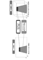
SAXS計測では遠視野強度単独計測に固有な曖昧性が現れうる。完全な空間情報は、電界振幅の二乗の絶対値として定義される実数値強度ではなく、複素数値の電界振幅の態で搬送される。加えて、弱いX線散乱の帰結として垂直方向曖昧性が生じうる。T−SAXSトモグラフィでは、硬X線に弱散乱特性があるため、被写体を垂直方向に沿い反転させても、大雑把には同じスペクトル整合となりうる。単純な長方形格子の場合、0次回折次数を計測することでスペクトルの曖昧性をなくすことができるが、その計測は現実には不可能であるので空間フラクション曖昧性が生じうる。T−SAXSトモグラフィでは、40%なるライン/空間フラクションを伴う2D格子が、60%なるライン/空間フラクションを伴う別の格子により表現され同じ計測信号に対し整合することがありうる。並進方向曖昧性は振幅に代え強度を計測することの直接的帰結である。図2には、同様の散乱を有するが周期的単位セル内定義が異なる諸2D構造例が描かれている。 In SAXS measurement, ambiguity peculiar to far-field intensity independent measurement may appear. Complete spatial information is carried in the form of complex-valued electric field amplitudes, rather than real-valued intensities defined as the absolute value of the square of the electric field amplitude. In addition, vertical ambiguity can occur as a result of weak X-ray scattering. In T-SAXS tomography, since hard X-rays have a weak scattering characteristic, even if the subject is inverted along the vertical direction, roughly the same spectral matching can be achieved. In the case of a simple rectangular lattice, the ambiguity of the spectrum can be eliminated by measuring the 0th order diffraction order, but since the measurement is not possible in reality, spatial fraction ambiguity may occur. In T-SAXS tomography, a 2D grid with 40% line / spatial fraction may be represented by another grid with 60% line / spatial fraction and matched to the same measurement signal. Translational ambiguity is a direct consequence of measuring intensity instead of amplitude. FIG. 2 depicts examples of 2D structures with similar scattering but different definitions within the periodic unit cell.
図3には付随計測による位相解明が描かれている。このモデルにおける未知位相は、付随計測を通じその構造のうち一部分を知り、それを周期的単位セル内で固定し、そして様々な照明角にて十分な個数の計測結果を採取してその構造の残りを判別することで、決定することができる。 In FIG. 3, the phase elucidation by the accompanying measurement is drawn. The unknown phase in this model knows a part of its structure through ancillary measurements, fixes it in a periodic unit cell, and collects a sufficient number of measurement results at various illumination angles for the rest of the structure. Can be determined by determining.
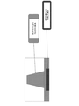
図4には先行計測による位相解明が描かれている。位相を判別できるよう、ターゲット構造の下方又は上方に付加的な既知構造が独立的に作成又は配置されている。ターゲット作成プロセス中の別工程にてその一部を計測することによっても、位相を判別することができる。 FIG. 4 depicts the phase elucidation by prior measurement. Additional known structures are independently created or placed below or above the target structure so that the phase can be determined. The phase can also be determined by measuring a part of the target in another process in the target creation process.
位相解明、例えば図4中のそれは、構造底部から構造頂部へと進行させうる。 Phase elucidation, eg, in FIG. 4, can proceed from the bottom of the structure to the top of the structure.
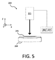
図5は一実施形態に係るウェハ計量ツール200のブロック図である。本ウェハ計量ツール200は、ウェハ205その他のワークピースを保持するよう構成されたチャック204を有している。チャック204は、一軸、二軸又は三軸に沿い移動又は回動させうるよう構成することができる。チャック204は、例えばZ軸周りで回転させうるようにも構成することができる。
FIG. 5 is a block diagram of the
ウェハ計量ツール200は、ウェハ205上にある面、デバイス、フィーチャ又は層のうち一部分を計測しうるよう構成された計測システム201をも有している。例えば、半導体ウェハ上にあるターゲットの表面を計測するようウェハ計量ツール200を構成することができる。ウェハ計量ツール200たりうるものにはCD−SEM、反射型小角X線スキャタロメータ、光スキャタロメータ等がある。例えば、ウェハ計量ツール200のハードウェア構成を特許文献1記載のそれに類するものとすることができるので、参照により同文献の全容を本願に繰り入れることにする。
The
ウェハ計量ツール200が反射型小角X線スキャタロメータ又は光スキャタロメータである場合、透過技術を用いるよう計測ツール(図5には描出せず)を構成し、それをプロセッサ202と電子通信させてもよい。その計測ツールたりうるものには透過型小角X線スキャタロメータがある。ウェハ計量ツール200は、更に、ターゲットの幾何形状を計測するよう構成することができる。
When the
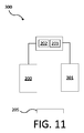
図11はシステム300のブロック図である。ウェハ計量ツール200及び計測ツール301の双方でウェハ205を撮像することができ、或いはその双方をウェハ205の諸性質の計測に用いることができる。ウェハ計量ツール200及び計測ツール301は、双方共、プロセッサ202及び電子データ格納ユニット203と電子通信する。ウェハ計量ツール200及び計測ツール301を同じシステムの構成部分としてもよいし、それらウェハ計量ツール200・計測ツール301間でウェハ205を移送することもできる。
FIG. 11 is a block diagram of the
翻って図5中の計測システム201によれば、光ビーム、電子ビーム、広帯域プラズマ等を生成することができ、或いはその他の技術を用いウェハ205の表面を計測することができる。一例に係る計測システム201はレーザを有するものである。別例に係るウェハ計量ツール200は広帯域プラズマ式検査ツールである。計測システム201によって、ウェハ205上にあるターゲットの画像を提供することや、ウェハ205上にあるダイの画像を形成するのに用いられる情報を提供することができる。
On the other hand, according to the
具体的には、ウェハ計量ツール200や計測システム201を、回動偏光子回動補償器分光エリプソメトリ(楕円偏向法)データ、全ミュラー行列成分データ、回動偏光子分光エリプソメトリデータ、リフレクトメトリ(反射計測法)データ、レーザ駆動分光リフレクトメトリデータ及びX線データのうち一種類又は複数種類を提供するよう、構成することができる。
Specifically, the
一例に係るウェハ計量ツール200は、広帯域光源と、その光源がターゲットとどう相互作用するかを計測する計測システム201と、そのターゲットの関連パラメタを抽出する処理アルゴリズムとを用い、分光エリプソメトリを実行する。その光源をレーザ駆動光源とすれば、Xeランプとは対照的に、高い強度を提供して検出器における信号対雑音比を高めることができよう。一例に係る集光システムは、一連のポラライザ(回動型又は固定型)、補償器(回動型又は固定型)、検出器、スペクトロメータ(分光計)、カメラ、レンズ、鏡及び/又はコリメータを有するものである。ターゲットシグネチャを増強することを狙い、本システムにて、N2又はArガスパージを用い波長域を170nm以下へと拡張してもよい。
The
ウェハ計量ツール200はプロセッサ202及び電子データ格納ユニット203と通信し、またその電子データ格納ユニット203がプロセッサ202と電子通信する。例えば、プロセッサ202は計測システム201その他、ウェハ計量ツール200の諸構成部材と通信することができる。プロセッサ202は、実際上、ハードウェア、ソフトウェア及びファームウェアの任意な組合せにより実現されうる。また、その諸機能であり本願記載のものを、単一ユニットにより実行してもよいし、相異なる構成部材間で分かち合ってもよいし、翻ってその構成部材それぞれをハードウェア、ソフトウェア及びファームウェアの任意な組合せにより実現してもよい。様々な方法及び機能をプロセッサ202にて実行・実現させるためのプログラムコード又は命令をコントローラ可読格納媒体内、例えば電子データ格納ユニット203内メモリ、プロセッサ202内メモリ、プロセッサ202外メモリ又はそれらの組合せに格納してもよい。
The
プロセッサ202及び電子データ格納ユニット203が1個しか描かれていないが、複数個のプロセッサ202及び/又は複数個の電子データ格納ユニット203を組み込むこともできる。各プロセッサ202の電子通信相手を電子データ格納ユニット203のうち1個又は複数個とすればよい。ある実施形態では1個又は複数個のプロセッサ202が可通信結合される。この場合、計測システム201にて受け取った読み値を当該1個又は複数個のプロセッサ202が受け取り、その読み値をプロセッサ202の電子データ格納ユニット203内に格納することができる。プロセッサ202及び/又は電子データ格納ユニット203は、ウェハ計量ツール200自体の一部であってもよいし、ウェハ計量ツール200とは別体であってもよい(例.スタンドアロン制御ユニットとし又は集中品質制御ユニット内におく)。
Although only one
プロセッサ202を、ウェハ計量ツール200の構成部材に対し何らかの好適な要領で(例.1個又は複数個の伝送媒体、例えば有線及び/又は無線伝送媒体を含むそれを介し)結合させることで、ウェハ計量ツール200により生成された出力、例えば計測システム201からの出力を、プロセッサ202にて受け取れるようにすることができる。その出力を用い多数の機能を実行するようプロセッサ202を構成することができる。例えば、ウェハ205上の諸層を計測するようプロセッサ202を構成することができる。また例えば、その出力を電子データ格納ユニット203その他の格納媒体へと出力レビュー抜きで送るよう、プロセッサ202を構成することができる。プロセッサ202は本願記載の如く更に構成することができる。
The
本願記載のプロセッサ202、その他のシステム(群)或いはその他のサブシステム(群)は、パーソナルコンピュータシステム、イメージコンピュータ、メインフレームコンピュータシステム、ワークステーション、ネットワーク機器、インターネット機器その他のデバイスを初め、様々な形態を採りうる。そのサブシステム(群)又はシステム(群)に、本件技術分野にて既知で好適な何らかのプロセッサ、例えば並列プロセッサを組み込むこともできる。加えて、そのサブシステム(群)又はシステム(群)に、スタンドアロンかネットワーク接続ツールかを問わず、高速処理及びソフトウェアを伴うプラットフォーム組み込むことができる。例えば、プロセッサ202にはマイクロプロセッサ、マイクロコントローラその他のデバイスが包含されうる。
The
システムが複数個のサブシステムを有しているのであれば、それら相異なるサブシステムを互いに結合させることで、画像、データ、情報、命令等々を、それらサブシステム間で送れるようにすることができる。例えば、あるサブシステムを、別のサブシステム(群)に、本件技術分野で既知なあらゆる好適有線及び/又は無線伝送媒体が含まれうる何れか好適な伝送媒体により、結合させればよい。それらサブシステムのうち2個以上を、共有型のコンピュータ可読格納媒体(図示せず)によって実質結合させてもよい。 If the system has multiple subsystems, the different subsystems can be combined with each other so that images, data, information, instructions, etc. can be sent between them. .. For example, one subsystem may be coupled to another subsystem (s) by any suitable transmission medium that may include any suitable wired and / or wireless transmission medium known in the art. Two or more of these subsystems may be substantially coupled by a shared computer-readable storage medium (not shown).
プロセッサ202は、欠陥レビューシステム、検査システム、計量システムその他、何らかの種類のシステムの一部分とすることもできる。即ち、本願開示の諸実施形態により記述されている幾つかの構成は、その能力が異なり用途の違いによりその好適性に多寡がある諸システム向けに、多様な要領で仕立てることができる。
プロセッサ202は、計測システム201その他、ウェハ計量ツール200の諸構成部材と電子通信することができる。プロセッサ202は本願記載の諸実施形態の何れに従い構成すればよい。プロセッサ202を、計測システム201の出力を用い、或いは他の源泉からの画像、計測結果又はデータを用い、他の諸機能又は付加的諸ステップを実現・実行するよう、構成してもよい。
The
ある付加的実施形態は、コントローラ上で実行可能なプログラム命令が格納された非一時的コンピュータ可読媒体、特に本願開示のコンピュータ実施方法を実行するためのそれに関するものである。とりわけ、図5に示すように、プロセッサ202に、電子データ格納ユニット203その他の電子データ格納媒体なる態のメモリを、プロセッサ202上で実行可能なプログラム命令入りの非一時的コンピュータ可読媒体と共に、組み込むことができる。そのコンピュータ実施方法には、本願記載の何れの方法(群)の何れのステップ(群)をも含めうる。例えば、方法100の諸ステップのうち一部又は全てを実行するよう、プロセッサ202に対しプログラミングしてもよい。電子データ格納ユニット203その他の電子データ格納媒体の態を採るメモリを格納媒体、例えば磁気又は光ディスク、磁気テープその他、本件技術分野にて既知で好適な何らかの非一時的コンピュータ可読媒体としてもよい。
One additional embodiment relates to a non-transitory computer-readable medium containing program instructions that can be executed on a controller, in particular for performing the computer implementation method disclosed in the present application. In particular, as shown in FIG. 5, a memory in the form of an electronic
一例としては、1個又は複数個のソフトウェアモジュールを実行するようプロセッサ202を構成することができる。例えば、期待物質の散乱密度を用い、表面のボクセルマップを、ウェハ計量ツール200から得られる計測結果の幾何に固定するよう、プロセッサ202を構成することができる。固定済表面ボクセル全ての散乱密度の均一スケーリングのみが行われることもある。電子データ格納ユニット203は、そのターゲット内の物質に関連付けられている複数個の散乱値が格納されるよう、構成することができる。プロセッサ202は、それらボクセルに関し一組の値から散乱値を採取するよう構成することができる。それら散乱値は連続的に浮動しうる。
As an example, the
それらプログラム命令は、就中、手続きベース技術、要素ベース技術及び/又はオブジェクト指向技術を初め、様々なやり方の何れで実現してもよい。例えば、それらプログラム命令を、ActiveX(登録商標)コントロール、C++オブジェクト、JavaBeans(登録商標)、Microsoft(登録商標)FoundationClasses(MFC)、ストリーミングSIMDエクステンション(SSE)その他のテクノロジ又は方法論を随意使用して実施すればよい。 These program instructions may be implemented in any of a variety of ways, including procedure-based technology, element-based technology and / or object-oriented technology, among others. For example, these program instructions may be implemented using ActiveX® controls, C ++ objects, JavaBeans®, Microsoft® Foundation Classes (MFC), Streaming SIMD Extensions (SSE) and other technologies or methodologies as desired. do it.
また、実施形態に係るプロセッサ202は、ウェハ計量ツール200に備わる様々な部材又はサブシステムの何れにも、本件技術分野で既知な何れかの要領で可通信結合させることができる。更に、伝送媒体例えば有線及び/又は無線区間を有するそれによって他システム(例.計測結果をもたらす検査システム例えばレビューツール、別の計測ツール、リモートデータベース内のデザインデータ等)からデータ又は情報を受領及び/又は獲得するよう、プロセッサ202を構成することができる。こうすることで、その伝送媒体を、プロセッサ202とそのウェハ計量ツール200の他サブシステムとの間、或いはウェハ計量ツール200外の諸システムとの間のデータリンクとして、働かせることができる。
Further, the
幾つかの実施形態では、本願開示のウェハ計量ツール200及び諸方法の様々なステップ、機能及び/又は動作が、電子回路、論理ゲート、マルチプレクサ、プログラマブル論理デバイス、ASIC、アナログ又はディジタルコントローラ/スイッチ、マイクロコントローラ並びに情報処理システムのうち、1個又は複数個により実行される。諸方法例えば本願記載のそれらを実現するプログラム命令を、キャリア媒体上で伝送してもよいし、その上に格納してもよい。そのキャリア媒体には格納媒体、例えばリードオンリメモリ、ランダムアクセスメモリ、磁気ディスク、光ディスク、不揮発性メモリ、固体メモリ、磁気テープ等が含まれうる。キャリア媒体には伝送媒体、例えばワイヤ、ケーブル又は無線伝送リンクも含まれうる。例えば、本件開示の随所に記載されている様々なステップを、単一のプロセッサ202(又はコンピュータシステム)により実行してもよいし、それに代え複数個のプロセッサ202(又は複数個のコンピュータシステム)により実行してもよい。更に、ウェハ計量ツール200に備わり相異なっているサブシステムが、1個又は複数個の情報処理又は論理システムを有していてもよい。従って、上掲の記載は、本件開示に対する限定としてではなく、単なる例証として解されるべきである。
In some embodiments, the various steps, functions and / or operations of the
一例としては、図5中のウェハ計量ツール200を、ターゲットを照明する照明システムと、ウェハ205上のターゲット、デバイス又はフィーチャと照明システムとの相互作用(又はその欠如)によりもたらされた関連情報を捉える計測システム201と、一通り又は複数通りのアルゴリズムを用い収集済情報を分析するプロセッサ202とを、有するものとすることができる。
As an example, the
ウェハ計量ツール200には、それを用い様々な半導体構造及び素材特性を計測しうる一通り又は複数通りのハードウェア構成を、組み込むことができる。そうしたハードウェア構成の例としては、これに限られるものではないが、分光エリプソメータ(分光楕円偏向計;SE)、複数通りの照明角を有するSE、ミュラー行列要素を(例.回動型補償器(群)を用い)計測するSE、単一波長エリプソメータ、ビームプロファイルエリプソメータ(角度分解エリプソメータ)、ビームプロファイルリフレクトメータ(角度分解リフレクトメータ(反射計))、広帯域反射スペクトロメータ(分光リフレクトメータ)、単一波長リフレクトメータ、角度分解リフレクトメータ、撮像システム、並びにスキャタロメータ(例.スペックルアナライザ)がある。それらハードウェア構成は、ディスクリートな動作システム群に分けることや、組み合わせて単一ツールにすることができる。
The
ある種のハードウェア構成に備わる照明システムを、1個又は複数個の光源を有するものとすることができる。その光源にて生成されうるものには、一波長しか有していない光(即ち単色光)、多数の離散波長を有する光(即ち多色光)、複数個の波長を有する光(即ち広帯域光)、及び/又は、連続的に又は波長ホッピングにより諸波長を通じ掃引される光(即ち可調又は掃引光源)がある。好適な光源の例には、白色光源、紫外(UV)レーザ、アークランプ又は無電極ランプ、レーザ維持プラズマ(LSP)光源、超連続体(超広帯域)光源例えば広帯域レーザ光源、或いはより短波長な光源例えばX線源、極端UV光源、或いはそれらの何らかの組合せがある。その光源を、十分な輝度を有する光をもたらすよう構成することもでき、場合によってはそれを約1W/(nm・cm2・Sr)超の輝度とすることができる。そのウェハ計量ツール200にその光源への高速フィードバックを組み込み、そのパワー及び波長を安定化させてもよい。その光源の出力は自由空間伝搬により送給することができ、場合によっては何らかの種類の光ファイバ又は光導波路を介し送給することができる。
The lighting system provided in some hardware configuration may have one or more light sources. What can be produced by the light source is light having only one wavelength (that is, monochromatic light), light having many discrete wavelengths (that is, multicolor light), and light having multiple wavelengths (that is, broadband light). And / or there is light (ie tuned or swept light source) that is swept through the wavelengths continuously or by wavelength hopping. Examples of suitable light sources include white light sources, ultraviolet (UV) lasers, arc lamps or electrodeless lamps, laser maintenance plasma (LSP) light sources, supercontinuous (ultra-wideband) light sources such as wideband laser light sources, or shorter wavelengths. There are light sources such as X-ray sources, extreme UV light sources, or some combination thereof. The light source can also be configured to provide light with sufficient luminance, which in some cases can have a luminance greater than about 1 W / (nm · cm 2 · Sr). The
ウェハ計量ツール200は、半導体製造に関連する多種多様な計測を行えるよう設計することができる。例えばある種の実施形態によれば、そのウェハ計量ツール200により1個又は複数個のターゲットの特性、例えば限界寸法、オーバレイ、サイドウォール(側壁)角、膜厚或いはプロセス関連パラメタ(例.焦点及び/又は照射量)を計測することができる。ターゲットたりうるものには、性質的に周期的なある種の注目領域、例えばメモリダイ内格子がある。ターゲットたりうるものには、複数個の層(又は膜)でありその厚みをウェハ計量ツール200により計測可能なものがある。ターゲットたりうるものには半導体ウェハ上に配置された(或いは既存の)ターゲットデザイン、例えばアライメント及び/又はオーバレイ位置揃え操作用のものがある。ターゲットの種類によっては、半導体ウェハ上の様々な個所に所在させることができる。例えば、ターゲットをスクライブライン内(例.ダイ間)に所在させること、及び/又は、ダイ自体の内部に所在させることができる。ある種の実施形態では、複数個のターゲットが同一又は複数個の計量ツールにより(同時に又は異時点で)計測される。そうした計測に由来するデータを組み合わせてもよい。計量ツールからのデータを半導体製造プロセスにて用いることで、例えばそのプロセス(例.リソグラフィ、エッチング)に補正量をフィードフォワード、フィードバック及び/又はフィードサイドウェイすることができ、従って無欠なプロセス制御ソリューションをもたらすことができる。
The
計測正確性と実デバイス特性への整合性とを改善するため、並びにインダイ又はオンデバイス計測を改善するため、様々な計量装置が提案されている。例えば、概ね反射性の光学系に依拠する集束ビームエリプソメトリ(楕円偏向法)を用いることができる。アポダイザを用いることで、光回折の効果のうち、幾何光学系により規定されるサイズを超えた照明スポットの広がりを引き起こす効果を、軽減することができる。高数値開口ツールを、同時複数入射角照明と併用することが、小ターゲット能を達成する別の途である。他計測例のなかには、半導体スタックを構成する一層又は複数層の組成を計測するもの、ウェハ上(又はウェハ内)におけるある種の欠陥を計測するもの、並びにフォトリソグラフィ輻射のうちウェハへの露出に供された分量を計測するものがあろう。場合によっては、非周期性ターゲットを計測すべく計量ツール及びアルゴリズムが構成されよう。 Various weighing devices have been proposed to improve measurement accuracy and consistency to real device characteristics, as well as to improve in-die or on-device measurements. For example, focused beam ellipsometry (ellipsometry), which relies largely on reflective optics, can be used. By using the apodizer, among the effects of light diffraction, the effect of causing the expansion of the illumination spot exceeding the size specified by the geometrical optics system can be reduced. Using the high numerical aperture tool in combination with simultaneous multiple incident angle illumination is another way to achieve small targeting capabilities. Other measurement examples include those that measure the composition of one or more layers that make up a semiconductor stack, those that measure certain defects on (or in) a wafer, and those that expose photolithography radiation to a wafer. There will be something to measure the amount provided. In some cases, weighing tools and algorithms may be configured to measure aperiodic targets.
注目パラメタの計測には、通常は複数のアルゴリズムが関わってくる。例えば、入射ビームと標本との光学相互作用については、電磁(EM)ソルバを用いモデル化することができ、且つ厳密結合波解析(RCWA)、有限要素法(FEM)、モーメント法、表面積分法、体積積分法、有限差分時間ドメイン(FDTD)その他といったアルゴリズムを用いることができる。注目ターゲットは、通常は幾何エンジンを用い、また場合によってはプロセスモデル化エンジンか両者の組合せを用い、モデル化(パラメタ表記)される。幾何エンジンは、例えばKLA−Tencorのソフトウェア製品たるAcuShape(登録商標)にて実現することができる。 Multiple algorithms are usually involved in the measurement of the parameter of interest. For example, the optical interaction between an incident beam and a specimen can be modeled using an electromagnetic (EM) solver and can be modeled using exact coupled wave analysis (RCWA), finite element method (FEM), moment method, surface integration method. , Volume integration method, finite difference time domain (FDTD) and others can be used. The target of interest is usually modeled (parameter notation) using a geometric engine and, in some cases, a process modeling engine or a combination of both. The geometry engine can be realized, for example, by AcuShape®, which is a software product of KLA-Tencor.
収集されたデータは、ライブラリ、高速次数低減モデル、回帰、機械学習アルゴリズム例えばニューラルネットワーク及びサポートベクタマシン(SVM)、次元縮退アルゴリズム例えば主成分分析(PCA)、独立成分分析(ICA)及び局所線形埋込(LLE)、スパース表現例えばフーリエ又はウェーブレット変換、カルマンフィルタ、同じ又は異なるツール種からのマッチングを促進するアルゴリズムその他を初め、多数のデータ当て嵌め及び最適化技術及びテクノロジにより分析することができる。収集されたデータを、モデル化、最適化及び/又は当て嵌めを含まないアルゴリズムにより分析することもできる。 The collected data is a library, fast order reduction model, regression, machine learning algorithms such as neural networks and support vector machines (SVM), dimension reduction algorithms such as principal component analysis (PCA), independent component analysis (ICA) and local linear padding. It can be analyzed by a number of data fitting and optimization techniques and technologies, including LLE, sparse representations such as Fourier or wavelet transformations, Kalman filters, algorithms that facilitate matching from the same or different tool types, and more. The collected data can also be analyzed by algorithms that do not include modeling, optimization and / or fitting.
情報処理アルゴリズムは、通常、情報処理ハードウェアの設計及び実現、並列化、分散情報処理、負荷バランシング、マルチサービスサポート又は動的負荷最適化等、一通り又は複数通りの手法を用いることで、諸計量アプリケーション向けに最適化される。相異なる実現形態のアルゴリズムを、ファームウェア、ソフトウェア、フィールドプログラマブルゲートアレイ(FPGA)及びプログラマブル光学素子等々の態にて実現することができる。 Information processing algorithms usually use one or more methods such as design and implementation of information processing hardware, parallelization, distributed information processing, load balancing, multi-service support or dynamic load optimization. Optimized for weighing applications. Algorithms of different implementation forms can be realized in the form of firmware, software, field programmable gate array (FPGA), programmable optical element, and the like.
そのデータ分析及び当て嵌めステップでは、通常、1個又は複数個の目標が追及される。その目標の例としては、CD、サイドウォール角(SWA)、形状、応力、組成、膜、バンドギャップ、電気特性、焦点/照射量、オーバレイ、生成プロセスパラメタ(例.レジスト状態、分圧、温度及び集束モデル)及び/又はそれらの任意の組合せの計測があろう。その目標が計量システムのモデル化及び/又は設計であってもよい。その目標が計量ターゲットのモデル化、設計及び/又は最適化であってもよい。 The data analysis and fitting steps usually pursue one or more goals. Examples of such goals are CD, sidewall angle (SWA), shape, stress, composition, film, bandgap, electrical characteristics, focus / irradiation, overlay, generation process parameters (eg, resist state, voltage division, temperature). And focusing models) and / or any combination thereof may be measured. The goal may be the modeling and / or design of the weighing system. The goal may be modeling, designing and / or optimization of the weighing target.
本件開示の諸実施形態は半導体計量の分野に対処するものであり、先に概括したハードウェア、アルゴリズム/ソフトウェア実現形態及びアーキテクチャ並びに用例に限定されるものではない。 The embodiments disclosed in the present disclosure address the field of semiconductor metric and are not limited to the hardware, algorithms / software implementations and architectures and examples outlined above.
本方法の各ステップは本願記載の如く実行されうる。それら方法には、本願記載のコントローラ及び/又はコンピュータサブシステム(群)若しくはシステム(群)により実行可能であれば、他のどのようなステップ(群)でも含めうる。それらステップを実行しうる1個又は複数個のコンピュータシステムを、本願記載の諸実施形態のうち何れに従い構成してもよい。加えて、上述の諸方法を、本願記載のシステム実施形態のうち何れにより実行してもよい。 Each step of the method can be performed as described in the present application. These methods may include any other step (group) as long as it is feasible by the controller and / or computer subsystem (group) or system (group) described in the present application. One or more computer systems capable of performing these steps may be configured according to any of the embodiments described in the present application. In addition, the above methods may be performed by any of the system embodiments described in the present application.
1個又は複数個の具体的実施形態を基準にして本件開示につき記述してきたが、理解し得るように、本件開示の技術的範囲から離隔することなく本件開示の他の諸実施形態をなすこともできる。即ち、本件開示は、添付する特許請求の範囲及びその合理的解釈によってのみ限定されるものと解される。
The disclosure has been described on the basis of one or more specific embodiments, but as can be understood, the other embodiments of the disclosure shall be made without deviating from the technical scope of the disclosure. You can also. That is, it is understood that the present disclosure is limited only by the claims and its rational interpretation attached.
Claims (20)
プロセッサを用いることで、幾何計測結果と整合させるべく且つ期待物質の散乱密度を用い前記表面のボクセルマップを固定する方法であり、固定済表面ボクセル全ての散乱密度の均一スケーリングが行われる方法。 A method of measuring the surface of a target on a semiconductor wafer using a wafer weighing tool, and then using a processor to fix the voxel map of the surface in order to match the geometric measurement results and using the scattering density of the expected substance. Yes, a method of uniform scaling of the scattering density of all fixed surface voxels.
前記ウェハ計量ツールと電子通信するプロセッサと、
を備え、前記プロセッサが、幾何計測結果と整合させるべく且つ期待物質の散乱密度を用い、前記表面のボクセルマップを固定するよう構成されており、固定済表面ボクセル全ての散乱密度の均一スケーリングが行われるシステム。 A wafer weighing tool configured to measure the surface of a target on a semiconductor wafer,
A processor that electronically communicates with the wafer weighing tool,
The processor is configured to fix the voxel map of the surface using the scattering density of the expected material in order to match the geometric measurement result, and the scattering density of all the fixed surface voxels is uniformly scaled. System.
The system according to claim 19, wherein the scattering value continuously floats.
Applications Claiming Priority (3)
| Application Number | Priority Date | Filing Date | Title |
|---|---|---|---|
| US16/047,818 US10677586B2 (en) | 2018-07-27 | 2018-07-27 | Phase revealing optical and X-ray semiconductor metrology |
| US16/047,818 | 2018-07-27 | ||
| PCT/US2019/043541 WO2020023810A1 (en) | 2018-07-27 | 2019-07-26 | Phase revealing optical and x-ray semiconductor metrology |
Publications (2)
| Publication Number | Publication Date |
|---|---|
| JP2021531663A true JP2021531663A (en) | 2021-11-18 |
| JP7303868B2 JP7303868B2 (en) | 2023-07-05 |
Family
ID=69182366
Family Applications (1)
| Application Number | Title | Priority Date | Filing Date |
|---|---|---|---|
| JP2021504446A Active JP7303868B2 (en) | 2018-07-27 | 2019-07-26 | Phase-resolved optics and X-ray semiconductor metrology |
Country Status (7)
| Country | Link |
|---|---|
| US (1) | US10677586B2 (en) |
| JP (1) | JP7303868B2 (en) |
| KR (1) | KR102518206B1 (en) |
| CN (1) | CN112368812B (en) |
| IL (1) | IL280009B2 (en) |
| TW (1) | TWI780347B (en) |
| WO (1) | WO2020023810A1 (en) |
Families Citing this family (3)
| Publication number | Priority date | Publication date | Assignee | Title |
|---|---|---|---|---|
| US11610297B2 (en) * | 2019-12-02 | 2023-03-21 | Kla Corporation | Tomography based semiconductor measurements using simplified models |
| WO2021179290A1 (en) * | 2020-03-13 | 2021-09-16 | Yangtze Memory Technologies Co., Ltd. | Systems and methods for semiconductor chip hole geometry metrology |
| US12288668B2 (en) * | 2023-05-11 | 2025-04-29 | Applied Materials Israel Ltd. | Entropy based image processing for focused ion beam delayer-edge slices detection |
Citations (3)
| Publication number | Priority date | Publication date | Assignee | Title |
|---|---|---|---|---|
| JPH06160064A (en) * | 1992-11-16 | 1994-06-07 | Mitsubishi Materials Shilicon Corp | Surface inspection method and inspection device |
| JP2002082063A (en) * | 2000-09-05 | 2002-03-22 | Komatsu Electronic Metals Co Ltd | Wafer surface inspection apparatus and inspection method |
| JP2010025836A (en) * | 2008-07-23 | 2010-02-04 | Hitachi High-Technologies Corp | Visual inspection method, visual inspection device, semiconductor inspection device, and semiconductor wafer cross-section inspection device |
Family Cites Families (22)
| Publication number | Priority date | Publication date | Assignee | Title |
|---|---|---|---|---|
| US5608526A (en) | 1995-01-19 | 1997-03-04 | Tencor Instruments | Focused beam spectroscopic ellipsometry method and system |
| US5859424A (en) | 1997-04-08 | 1999-01-12 | Kla-Tencor Corporation | Apodizing filter system useful for reducing spot size in optical measurements and other applications |
| US6429943B1 (en) | 2000-03-29 | 2002-08-06 | Therma-Wave, Inc. | Critical dimension analysis with simultaneous multiple angle of incidence measurements |
| US7478019B2 (en) | 2005-01-26 | 2009-01-13 | Kla-Tencor Corporation | Multiple tool and structure analysis |
| US7567351B2 (en) | 2006-02-02 | 2009-07-28 | Kla-Tencor Corporation | High resolution monitoring of CD variations |
| CN101359611B (en) * | 2007-07-30 | 2011-11-09 | 东京毅力科创株式会社 | Selected variable optimization for optical metering system |
| EP2748793B1 (en) | 2011-10-14 | 2017-10-11 | Ingrain, Inc. | Dual image method and system for generating a multi-dimensional image of a sample |
| WO2013158593A1 (en) * | 2012-04-18 | 2013-10-24 | Kla-Tencor Corporation | Critical dimension uniformity monitoring for extreme ultra-violet reticles |
| US10013518B2 (en) * | 2012-07-10 | 2018-07-03 | Kla-Tencor Corporation | Model building and analysis engine for combined X-ray and optical metrology |
| WO2014062972A1 (en) | 2012-10-18 | 2014-04-24 | Kla-Tencor Corporation | Symmetric target design in scatterometry overlay metrology |
| US9581430B2 (en) | 2012-10-19 | 2017-02-28 | Kla-Tencor Corporation | Phase characterization of targets |
| JP5974840B2 (en) | 2012-11-07 | 2016-08-23 | ソニー株式会社 | Simulation method, simulation program, simulator, processing apparatus, semiconductor device manufacturing method |
| US10769320B2 (en) | 2012-12-18 | 2020-09-08 | Kla-Tencor Corporation | Integrated use of model-based metrology and a process model |
| US9291554B2 (en) | 2013-02-05 | 2016-03-22 | Kla-Tencor Corporation | Method of electromagnetic modeling of finite structures and finite illumination for metrology and inspection |
| US10101670B2 (en) | 2013-03-27 | 2018-10-16 | Kla-Tencor Corporation | Statistical model-based metrology |
| US9915522B1 (en) | 2013-06-03 | 2018-03-13 | Kla-Tencor Corporation | Optimized spatial modeling for optical CD metrology |
| US9494535B2 (en) | 2014-04-21 | 2016-11-15 | Kla-Tencor Corporation | Scatterometry-based imaging and critical dimension metrology |
| US9874526B2 (en) | 2016-03-28 | 2018-01-23 | Kla-Tencor Corporation | Methods and apparatus for polarized wafer inspection |
| EP3240013B1 (en) * | 2016-04-26 | 2018-11-07 | FEI Company | Three-dimensional imaging in charged-particle microscopy |
| SG11201902745RA (en) * | 2016-10-17 | 2019-05-30 | Kla Tencor Corp | Optimizing training sets used for setting up inspection-related algorithms |
| US10775323B2 (en) * | 2016-10-18 | 2020-09-15 | Kla-Tencor Corporation | Full beam metrology for X-ray scatterometry systems |
| US10382699B2 (en) * | 2016-12-01 | 2019-08-13 | Varjo Technologies Oy | Imaging system and method of producing images for display apparatus |
-
2018
- 2018-07-27 US US16/047,818 patent/US10677586B2/en active Active
-
2019
- 2019-07-11 TW TW108124425A patent/TWI780347B/en active
- 2019-07-26 WO PCT/US2019/043541 patent/WO2020023810A1/en not_active Ceased
- 2019-07-26 CN CN201980045267.3A patent/CN112368812B/en active Active
- 2019-07-26 JP JP2021504446A patent/JP7303868B2/en active Active
- 2019-07-26 KR KR1020217005462A patent/KR102518206B1/en active Active
-
2021
- 2021-01-07 IL IL280009A patent/IL280009B2/en unknown
Patent Citations (3)
| Publication number | Priority date | Publication date | Assignee | Title |
|---|---|---|---|---|
| JPH06160064A (en) * | 1992-11-16 | 1994-06-07 | Mitsubishi Materials Shilicon Corp | Surface inspection method and inspection device |
| JP2002082063A (en) * | 2000-09-05 | 2002-03-22 | Komatsu Electronic Metals Co Ltd | Wafer surface inspection apparatus and inspection method |
| JP2010025836A (en) * | 2008-07-23 | 2010-02-04 | Hitachi High-Technologies Corp | Visual inspection method, visual inspection device, semiconductor inspection device, and semiconductor wafer cross-section inspection device |
Also Published As
| Publication number | Publication date |
|---|---|
| CN112368812A (en) | 2021-02-12 |
| TW202007958A (en) | 2020-02-16 |
| TWI780347B (en) | 2022-10-11 |
| KR20210027497A (en) | 2021-03-10 |
| KR102518206B1 (en) | 2023-04-04 |
| CN112368812B (en) | 2022-03-25 |
| IL280009A (en) | 2021-03-01 |
| IL280009B2 (en) | 2023-07-01 |
| US20200080836A1 (en) | 2020-03-12 |
| IL280009B1 (en) | 2023-03-01 |
| WO2020023810A1 (en) | 2020-01-30 |
| US10677586B2 (en) | 2020-06-09 |
| JP7303868B2 (en) | 2023-07-05 |
Similar Documents
| Publication | Publication Date | Title |
|---|---|---|
| TWI760309B (en) | System, method and computer program product for calibration of metrology tools | |
| KR102220435B1 (en) | Measurement model optimization based on parameter variations across a wafer | |
| CN111566674B (en) | Automatic optimization of measurement accuracy through advanced machine learning technology | |
| CN104395996B (en) | Measurement formulation optimization based on spectrum sensitivity and technique change | |
| CN107408519B (en) | System and method for model-based single parameter measurement | |
| KR102245695B1 (en) | Integrated use of model-based metrology and a process model | |
| KR102055966B1 (en) | Model building and analysis engine, method, and computer-readable medium for combined x-ray and optical metrology | |
| KR102046216B1 (en) | Combined x-ray and optical metrology | |
| US10705434B2 (en) | Verification metrology target and their design | |
| KR101860042B1 (en) | Method and apparatus for design of a metrology target | |
| KR20220107326A (en) | Signal response metrology for image based and scatterometry overlay measurements | |
| CN104838251A (en) | Apparatus and method for optical metrology with optimized system parameters | |
| CN106463430A (en) | Devices, techniques and target design for measuring semiconductor parameters | |
| KR20200086746A (en) | Methodology for measuring advanced nanostructures | |
| CN114746991A (en) | Tomography-based semiconductor measurements using simplified models | |
| US8875078B2 (en) | Reference library generation method for methods of inspection, inspection apparatus and lithographic apparatus | |
| US9347872B1 (en) | Meta-model based measurement refinement | |
| JP7303868B2 (en) | Phase-resolved optics and X-ray semiconductor metrology | |
| TWI667548B (en) | Inspection method and apparatus and lithographic apparatus | |
| TW202536398A (en) | Method for determining an optical property of a multi-layer structure |
Legal Events
| Date | Code | Title | Description |
|---|---|---|---|
| A621 | Written request for application examination |
Free format text: JAPANESE INTERMEDIATE CODE: A621 Effective date: 20220720 |
|
| A871 | Explanation of circumstances concerning accelerated examination |
Free format text: JAPANESE INTERMEDIATE CODE: A871 Effective date: 20220720 |
|
| A131 | Notification of reasons for refusal |
Free format text: JAPANESE INTERMEDIATE CODE: A131 Effective date: 20221025 |
|
| A521 | Request for written amendment filed |
Free format text: JAPANESE INTERMEDIATE CODE: A523 Effective date: 20230118 |
|
| A131 | Notification of reasons for refusal |
Free format text: JAPANESE INTERMEDIATE CODE: A131 Effective date: 20230307 |
|
| A521 | Request for written amendment filed |
Free format text: JAPANESE INTERMEDIATE CODE: A523 Effective date: 20230601 |
|
| TRDD | Decision of grant or rejection written | ||
| A01 | Written decision to grant a patent or to grant a registration (utility model) |
Free format text: JAPANESE INTERMEDIATE CODE: A01 Effective date: 20230613 |
|
| A61 | First payment of annual fees (during grant procedure) |
Free format text: JAPANESE INTERMEDIATE CODE: A61 Effective date: 20230623 |
|
| R150 | Certificate of patent or registration of utility model |
Ref document number: 7303868 Country of ref document: JP Free format text: JAPANESE INTERMEDIATE CODE: R150 |