JP2019519087A - Array imaging module and molded photosensitive assembly, and method of manufacturing the same for electronic devices - Google Patents
Array imaging module and molded photosensitive assembly, and method of manufacturing the same for electronic devices Download PDFInfo
- Publication number
- JP2019519087A JP2019519087A JP2018547880A JP2018547880A JP2019519087A JP 2019519087 A JP2019519087 A JP 2019519087A JP 2018547880 A JP2018547880 A JP 2018547880A JP 2018547880 A JP2018547880 A JP 2018547880A JP 2019519087 A JP2019519087 A JP 2019519087A
- Authority
- JP
- Japan
- Prior art keywords
- photosensitive
- chip
- circuit board
- mold
- imaging module
- Prior art date
- Legal status (The legal status is an assumption and is not a legal conclusion. Google has not performed a legal analysis and makes no representation as to the accuracy of the status listed.)
- Pending
Links
- 238000003384 imaging method Methods 0.000 title claims abstract description 364
- 238000004519 manufacturing process Methods 0.000 title claims description 73
- 230000003287 optical effect Effects 0.000 claims abstract description 216
- 230000008878 coupling Effects 0.000 claims abstract description 48
- 238000010168 coupling process Methods 0.000 claims abstract description 48
- 238000005859 coupling reaction Methods 0.000 claims abstract description 48
- 238000000034 method Methods 0.000 claims description 165
- 238000000465 moulding Methods 0.000 claims description 72
- 230000002093 peripheral effect Effects 0.000 claims description 66
- 239000000463 material Substances 0.000 claims description 43
- 230000003014 reinforcing effect Effects 0.000 claims description 30
- 239000000758 substrate Substances 0.000 claims description 25
- 239000000853 adhesive Substances 0.000 claims description 20
- 230000001070 adhesive effect Effects 0.000 claims description 20
- 238000005538 encapsulation Methods 0.000 claims description 19
- PCHJSUWPFVWCPO-UHFFFAOYSA-N gold Chemical compound [Au] PCHJSUWPFVWCPO-UHFFFAOYSA-N 0.000 claims description 12
- 239000000945 filler Substances 0.000 claims description 11
- 229920000106 Liquid crystal polymer Polymers 0.000 claims description 8
- 239000004977 Liquid-crystal polymers (LCPs) Substances 0.000 claims description 8
- 239000004743 Polypropylene Substances 0.000 claims description 8
- 229910052751 metal Inorganic materials 0.000 claims description 8
- 239000002184 metal Substances 0.000 claims description 8
- 239000003990 capacitor Substances 0.000 claims description 7
- 230000017525 heat dissipation Effects 0.000 claims description 7
- RYGMFSIKBFXOCR-UHFFFAOYSA-N Copper Chemical compound [Cu] RYGMFSIKBFXOCR-UHFFFAOYSA-N 0.000 claims description 5
- BQCADISMDOOEFD-UHFFFAOYSA-N Silver Chemical compound [Ag] BQCADISMDOOEFD-UHFFFAOYSA-N 0.000 claims description 5
- 239000004677 Nylon Substances 0.000 claims description 4
- 229910052782 aluminium Inorganic materials 0.000 claims description 4
- XAGFODPZIPBFFR-UHFFFAOYSA-N aluminium Chemical compound [Al] XAGFODPZIPBFFR-UHFFFAOYSA-N 0.000 claims description 4
- 239000000919 ceramic Substances 0.000 claims description 4
- 229920001778 nylon Polymers 0.000 claims description 4
- -1 polypropylene Polymers 0.000 claims description 4
- 229920001155 polypropylene Polymers 0.000 claims description 4
- 238000005345 coagulation Methods 0.000 claims description 3
- 238000007493 shaping process Methods 0.000 claims description 2
- 230000007480 spreading Effects 0.000 claims description 2
- 238000003892 spreading Methods 0.000 claims description 2
- 206010034972 Photosensitivity reaction Diseases 0.000 claims 2
- 230000036211 photosensitivity Effects 0.000 claims 2
- 229910052802 copper Inorganic materials 0.000 claims 1
- 239000010949 copper Substances 0.000 claims 1
- 239000010931 gold Substances 0.000 claims 1
- 229910052737 gold Inorganic materials 0.000 claims 1
- 229910052709 silver Inorganic materials 0.000 claims 1
- 239000004332 silver Substances 0.000 claims 1
- WABPQHHGFIMREM-UHFFFAOYSA-N lead(0) Chemical compound [Pb] WABPQHHGFIMREM-UHFFFAOYSA-N 0.000 abstract description 29
- 230000008569 process Effects 0.000 description 89
- 230000008901 benefit Effects 0.000 description 36
- 230000009977 dual effect Effects 0.000 description 22
- 238000003466 welding Methods 0.000 description 17
- 239000012778 molding material Substances 0.000 description 12
- 238000011109 contamination Methods 0.000 description 11
- 238000007711 solidification Methods 0.000 description 10
- 230000008023 solidification Effects 0.000 description 10
- 238000005516 engineering process Methods 0.000 description 8
- 230000002787 reinforcement Effects 0.000 description 8
- 239000000428 dust Substances 0.000 description 7
- 230000000694 effects Effects 0.000 description 6
- 238000001746 injection moulding Methods 0.000 description 6
- 239000011265 semifinished product Substances 0.000 description 5
- 230000000712 assembly Effects 0.000 description 4
- 238000000429 assembly Methods 0.000 description 4
- 238000010586 diagram Methods 0.000 description 4
- 239000007787 solid Substances 0.000 description 4
- 230000003595 spectral effect Effects 0.000 description 4
- 230000002411 adverse Effects 0.000 description 3
- 238000006243 chemical reaction Methods 0.000 description 3
- 239000002131 composite material Substances 0.000 description 3
- 239000000356 contaminant Substances 0.000 description 3
- 239000012530 fluid Substances 0.000 description 3
- 239000007788 liquid Substances 0.000 description 3
- 238000012986 modification Methods 0.000 description 3
- 230000004048 modification Effects 0.000 description 3
- 238000007789 sealing Methods 0.000 description 3
- 239000003795 chemical substances by application Substances 0.000 description 2
- 230000015271 coagulation Effects 0.000 description 2
- 238000004891 communication Methods 0.000 description 2
- 230000001186 cumulative effect Effects 0.000 description 2
- 238000006073 displacement reaction Methods 0.000 description 2
- 238000009434 installation Methods 0.000 description 2
- 238000009413 insulation Methods 0.000 description 2
- 239000000203 mixture Substances 0.000 description 2
- 239000002245 particle Substances 0.000 description 2
- 239000011236 particulate material Substances 0.000 description 2
- 239000000843 powder Substances 0.000 description 2
- 239000004065 semiconductor Substances 0.000 description 2
- 238000012546 transfer Methods 0.000 description 2
- 238000009966 trimming Methods 0.000 description 2
- 206010027146 Melanoderma Diseases 0.000 description 1
- 230000015572 biosynthetic process Effects 0.000 description 1
- 230000001413 cellular effect Effects 0.000 description 1
- 150000001875 compounds Chemical class 0.000 description 1
- 238000007796 conventional method Methods 0.000 description 1
- 238000001816 cooling Methods 0.000 description 1
- 238000005520 cutting process Methods 0.000 description 1
- 238000011161 development Methods 0.000 description 1
- 238000001914 filtration Methods 0.000 description 1
- 238000010438 heat treatment Methods 0.000 description 1
- 238000002513 implantation Methods 0.000 description 1
- 238000007373 indentation Methods 0.000 description 1
- 230000006698 induction Effects 0.000 description 1
- 239000011344 liquid material Substances 0.000 description 1
- 231100000289 photo-effect Toxicity 0.000 description 1
- 230000002165 photosensitisation Effects 0.000 description 1
- 238000007747 plating Methods 0.000 description 1
- 239000000047 product Substances 0.000 description 1
- 239000000565 sealant Substances 0.000 description 1
- 230000006641 stabilisation Effects 0.000 description 1
- 238000011105 stabilization Methods 0.000 description 1
- 230000003319 supportive effect Effects 0.000 description 1
- 238000003786 synthesis reaction Methods 0.000 description 1
- 239000012815 thermoplastic material Substances 0.000 description 1
- 230000007704 transition Effects 0.000 description 1
Images


Classifications
-
- G—PHYSICS
- G02—OPTICS
- G02B—OPTICAL ELEMENTS, SYSTEMS OR APPARATUS
- G02B7/00—Mountings, adjusting means, or light-tight connections, for optical elements
- G02B7/02—Mountings, adjusting means, or light-tight connections, for optical elements for lenses
- G02B7/021—Mountings, adjusting means, or light-tight connections, for optical elements for lenses for more than one lens
-
- H—ELECTRICITY
- H04—ELECTRIC COMMUNICATION TECHNIQUE
- H04N—PICTORIAL COMMUNICATION, e.g. TELEVISION
- H04N23/00—Cameras or camera modules comprising electronic image sensors; Control thereof
- H04N23/50—Constructional details
-
- B—PERFORMING OPERATIONS; TRANSPORTING
- B29—WORKING OF PLASTICS; WORKING OF SUBSTANCES IN A PLASTIC STATE IN GENERAL
- B29C—SHAPING OR JOINING OF PLASTICS; SHAPING OF MATERIAL IN A PLASTIC STATE, NOT OTHERWISE PROVIDED FOR; AFTER-TREATMENT OF THE SHAPED PRODUCTS, e.g. REPAIRING
- B29C45/00—Injection moulding, i.e. forcing the required volume of moulding material through a nozzle into a closed mould; Apparatus therefor
- B29C45/14—Injection moulding, i.e. forcing the required volume of moulding material through a nozzle into a closed mould; Apparatus therefor incorporating preformed parts or layers, e.g. injection moulding around inserts or for coating articles
- B29C45/14639—Injection moulding, i.e. forcing the required volume of moulding material through a nozzle into a closed mould; Apparatus therefor incorporating preformed parts or layers, e.g. injection moulding around inserts or for coating articles for obtaining an insulating effect, e.g. for electrical components
-
- G—PHYSICS
- G02—OPTICS
- G02B—OPTICAL ELEMENTS, SYSTEMS OR APPARATUS
- G02B13/00—Optical objectives specially designed for the purposes specified below
- G02B13/001—Miniaturised objectives for electronic devices, e.g. portable telephones, webcams, PDAs, small digital cameras
-
- G—PHYSICS
- G02—OPTICS
- G02B—OPTICAL ELEMENTS, SYSTEMS OR APPARATUS
- G02B13/00—Optical objectives specially designed for the purposes specified below
- G02B13/001—Miniaturised objectives for electronic devices, e.g. portable telephones, webcams, PDAs, small digital cameras
- G02B13/0015—Miniaturised objectives for electronic devices, e.g. portable telephones, webcams, PDAs, small digital cameras characterised by the lens design
- G02B13/002—Miniaturised objectives for electronic devices, e.g. portable telephones, webcams, PDAs, small digital cameras characterised by the lens design having at least one aspherical surface
- G02B13/004—Miniaturised objectives for electronic devices, e.g. portable telephones, webcams, PDAs, small digital cameras characterised by the lens design having at least one aspherical surface having four lenses
-
- G—PHYSICS
- G02—OPTICS
- G02B—OPTICAL ELEMENTS, SYSTEMS OR APPARATUS
- G02B3/00—Simple or compound lenses
- G02B3/0006—Arrays
- G02B3/0075—Arrays characterized by non-optical structures, e.g. having integrated holding or alignment means
-
- G—PHYSICS
- G02—OPTICS
- G02B—OPTICAL ELEMENTS, SYSTEMS OR APPARATUS
- G02B5/00—Optical elements other than lenses
- G02B5/20—Filters
- G02B5/201—Filters in the form of arrays
-
- G—PHYSICS
- G02—OPTICS
- G02B—OPTICAL ELEMENTS, SYSTEMS OR APPARATUS
- G02B7/00—Mountings, adjusting means, or light-tight connections, for optical elements
- G02B7/006—Filter holders
-
- H—ELECTRICITY
- H01—ELECTRIC ELEMENTS
- H01L—SEMICONDUCTOR DEVICES NOT COVERED BY CLASS H10
- H01L25/00—Assemblies consisting of a plurality of individual semiconductor or other solid state devices ; Multistep manufacturing processes thereof
- H01L25/50—Multistep manufacturing processes of assemblies consisting of devices, each device being of a type provided for in group H01L27/00 or H01L29/00
-
- H—ELECTRICITY
- H01—ELECTRIC ELEMENTS
- H01L—SEMICONDUCTOR DEVICES NOT COVERED BY CLASS H10
- H01L27/00—Devices consisting of a plurality of semiconductor or other solid-state components formed in or on a common substrate
- H01L27/14—Devices consisting of a plurality of semiconductor or other solid-state components formed in or on a common substrate including semiconductor components sensitive to infrared radiation, light, electromagnetic radiation of shorter wavelength or corpuscular radiation and specially adapted either for the conversion of the energy of such radiation into electrical energy or for the control of electrical energy by such radiation
- H01L27/144—Devices controlled by radiation
- H01L27/146—Imager structures
- H01L27/14601—Structural or functional details thereof
- H01L27/14618—Containers
-
- H—ELECTRICITY
- H01—ELECTRIC ELEMENTS
- H01L—SEMICONDUCTOR DEVICES NOT COVERED BY CLASS H10
- H01L27/00—Devices consisting of a plurality of semiconductor or other solid-state components formed in or on a common substrate
- H01L27/14—Devices consisting of a plurality of semiconductor or other solid-state components formed in or on a common substrate including semiconductor components sensitive to infrared radiation, light, electromagnetic radiation of shorter wavelength or corpuscular radiation and specially adapted either for the conversion of the energy of such radiation into electrical energy or for the control of electrical energy by such radiation
- H01L27/144—Devices controlled by radiation
- H01L27/146—Imager structures
- H01L27/14601—Structural or functional details thereof
- H01L27/1462—Coatings
- H01L27/14621—Colour filter arrangements
-
- H—ELECTRICITY
- H01—ELECTRIC ELEMENTS
- H01L—SEMICONDUCTOR DEVICES NOT COVERED BY CLASS H10
- H01L27/00—Devices consisting of a plurality of semiconductor or other solid-state components formed in or on a common substrate
- H01L27/14—Devices consisting of a plurality of semiconductor or other solid-state components formed in or on a common substrate including semiconductor components sensitive to infrared radiation, light, electromagnetic radiation of shorter wavelength or corpuscular radiation and specially adapted either for the conversion of the energy of such radiation into electrical energy or for the control of electrical energy by such radiation
- H01L27/144—Devices controlled by radiation
- H01L27/146—Imager structures
- H01L27/14601—Structural or functional details thereof
- H01L27/14625—Optical elements or arrangements associated with the device
- H01L27/14627—Microlenses
-
- H—ELECTRICITY
- H01—ELECTRIC ELEMENTS
- H01L—SEMICONDUCTOR DEVICES NOT COVERED BY CLASS H10
- H01L27/00—Devices consisting of a plurality of semiconductor or other solid-state components formed in or on a common substrate
- H01L27/14—Devices consisting of a plurality of semiconductor or other solid-state components formed in or on a common substrate including semiconductor components sensitive to infrared radiation, light, electromagnetic radiation of shorter wavelength or corpuscular radiation and specially adapted either for the conversion of the energy of such radiation into electrical energy or for the control of electrical energy by such radiation
- H01L27/144—Devices controlled by radiation
- H01L27/146—Imager structures
- H01L27/14601—Structural or functional details thereof
- H01L27/14634—Assemblies, i.e. Hybrid structures
-
- H—ELECTRICITY
- H01—ELECTRIC ELEMENTS
- H01L—SEMICONDUCTOR DEVICES NOT COVERED BY CLASS H10
- H01L27/00—Devices consisting of a plurality of semiconductor or other solid-state components formed in or on a common substrate
- H01L27/14—Devices consisting of a plurality of semiconductor or other solid-state components formed in or on a common substrate including semiconductor components sensitive to infrared radiation, light, electromagnetic radiation of shorter wavelength or corpuscular radiation and specially adapted either for the conversion of the energy of such radiation into electrical energy or for the control of electrical energy by such radiation
- H01L27/144—Devices controlled by radiation
- H01L27/146—Imager structures
- H01L27/14683—Processes or apparatus peculiar to the manufacture or treatment of these devices or parts thereof
- H01L27/14685—Process for coatings or optical elements
-
- H—ELECTRICITY
- H01—ELECTRIC ELEMENTS
- H01L—SEMICONDUCTOR DEVICES NOT COVERED BY CLASS H10
- H01L27/00—Devices consisting of a plurality of semiconductor or other solid-state components formed in or on a common substrate
- H01L27/14—Devices consisting of a plurality of semiconductor or other solid-state components formed in or on a common substrate including semiconductor components sensitive to infrared radiation, light, electromagnetic radiation of shorter wavelength or corpuscular radiation and specially adapted either for the conversion of the energy of such radiation into electrical energy or for the control of electrical energy by such radiation
- H01L27/144—Devices controlled by radiation
- H01L27/146—Imager structures
- H01L27/14683—Processes or apparatus peculiar to the manufacture or treatment of these devices or parts thereof
- H01L27/14687—Wafer level processing
-
- H—ELECTRICITY
- H01—ELECTRIC ELEMENTS
- H01L—SEMICONDUCTOR DEVICES NOT COVERED BY CLASS H10
- H01L27/00—Devices consisting of a plurality of semiconductor or other solid-state components formed in or on a common substrate
- H01L27/14—Devices consisting of a plurality of semiconductor or other solid-state components formed in or on a common substrate including semiconductor components sensitive to infrared radiation, light, electromagnetic radiation of shorter wavelength or corpuscular radiation and specially adapted either for the conversion of the energy of such radiation into electrical energy or for the control of electrical energy by such radiation
- H01L27/144—Devices controlled by radiation
- H01L27/146—Imager structures
- H01L27/14683—Processes or apparatus peculiar to the manufacture or treatment of these devices or parts thereof
- H01L27/1469—Assemblies, i.e. hybrid integration
-
- H—ELECTRICITY
- H04—ELECTRIC COMMUNICATION TECHNIQUE
- H04N—PICTORIAL COMMUNICATION, e.g. TELEVISION
- H04N23/00—Cameras or camera modules comprising electronic image sensors; Control thereof
- H04N23/45—Cameras or camera modules comprising electronic image sensors; Control thereof for generating image signals from two or more image sensors being of different type or operating in different modes, e.g. with a CMOS sensor for moving images in combination with a charge-coupled device [CCD] for still images
-
- H—ELECTRICITY
- H04—ELECTRIC COMMUNICATION TECHNIQUE
- H04N—PICTORIAL COMMUNICATION, e.g. TELEVISION
- H04N23/00—Cameras or camera modules comprising electronic image sensors; Control thereof
- H04N23/50—Constructional details
- H04N23/51—Housings
-
- H—ELECTRICITY
- H04—ELECTRIC COMMUNICATION TECHNIQUE
- H04N—PICTORIAL COMMUNICATION, e.g. TELEVISION
- H04N23/00—Cameras or camera modules comprising electronic image sensors; Control thereof
- H04N23/50—Constructional details
- H04N23/54—Mounting of pick-up tubes, electronic image sensors, deviation or focusing coils
-
- H—ELECTRICITY
- H04—ELECTRIC COMMUNICATION TECHNIQUE
- H04N—PICTORIAL COMMUNICATION, e.g. TELEVISION
- H04N23/00—Cameras or camera modules comprising electronic image sensors; Control thereof
- H04N23/50—Constructional details
- H04N23/55—Optical parts specially adapted for electronic image sensors; Mounting thereof
-
- H—ELECTRICITY
- H04—ELECTRIC COMMUNICATION TECHNIQUE
- H04N—PICTORIAL COMMUNICATION, e.g. TELEVISION
- H04N23/00—Cameras or camera modules comprising electronic image sensors; Control thereof
- H04N23/57—Mechanical or electrical details of cameras or camera modules specially adapted for being embedded in other devices
-
- H—ELECTRICITY
- H05—ELECTRIC TECHNIQUES NOT OTHERWISE PROVIDED FOR
- H05K—PRINTED CIRCUITS; CASINGS OR CONSTRUCTIONAL DETAILS OF ELECTRIC APPARATUS; MANUFACTURE OF ASSEMBLAGES OF ELECTRICAL COMPONENTS
- H05K1/00—Printed circuits
- H05K1/02—Details
- H05K1/0201—Thermal arrangements, e.g. for cooling, heating or preventing overheating
- H05K1/0203—Cooling of mounted components
-
- H—ELECTRICITY
- H05—ELECTRIC TECHNIQUES NOT OTHERWISE PROVIDED FOR
- H05K—PRINTED CIRCUITS; CASINGS OR CONSTRUCTIONAL DETAILS OF ELECTRIC APPARATUS; MANUFACTURE OF ASSEMBLAGES OF ELECTRICAL COMPONENTS
- H05K1/00—Printed circuits
- H05K1/02—Details
- H05K1/0274—Optical details, e.g. printed circuits comprising integral optical means
-
- H—ELECTRICITY
- H05—ELECTRIC TECHNIQUES NOT OTHERWISE PROVIDED FOR
- H05K—PRINTED CIRCUITS; CASINGS OR CONSTRUCTIONAL DETAILS OF ELECTRIC APPARATUS; MANUFACTURE OF ASSEMBLAGES OF ELECTRICAL COMPONENTS
- H05K1/00—Printed circuits
- H05K1/18—Printed circuits structurally associated with non-printed electric components
- H05K1/182—Printed circuits structurally associated with non-printed electric components associated with components mounted in the printed circuit board, e.g. insert mounted components [IMC]
- H05K1/183—Components mounted in and supported by recessed areas of the printed circuit board
-
- H—ELECTRICITY
- H05—ELECTRIC TECHNIQUES NOT OTHERWISE PROVIDED FOR
- H05K—PRINTED CIRCUITS; CASINGS OR CONSTRUCTIONAL DETAILS OF ELECTRIC APPARATUS; MANUFACTURE OF ASSEMBLAGES OF ELECTRICAL COMPONENTS
- H05K1/00—Printed circuits
- H05K1/18—Printed circuits structurally associated with non-printed electric components
- H05K1/182—Printed circuits structurally associated with non-printed electric components associated with components mounted in the printed circuit board, e.g. insert mounted components [IMC]
- H05K1/185—Components encapsulated in the insulating substrate of the printed circuit or incorporated in internal layers of a multilayer circuit
-
- H—ELECTRICITY
- H05—ELECTRIC TECHNIQUES NOT OTHERWISE PROVIDED FOR
- H05K—PRINTED CIRCUITS; CASINGS OR CONSTRUCTIONAL DETAILS OF ELECTRIC APPARATUS; MANUFACTURE OF ASSEMBLAGES OF ELECTRICAL COMPONENTS
- H05K1/00—Printed circuits
- H05K1/18—Printed circuits structurally associated with non-printed electric components
- H05K1/189—Printed circuits structurally associated with non-printed electric components characterised by the use of a flexible or folded printed circuit
-
- H—ELECTRICITY
- H05—ELECTRIC TECHNIQUES NOT OTHERWISE PROVIDED FOR
- H05K—PRINTED CIRCUITS; CASINGS OR CONSTRUCTIONAL DETAILS OF ELECTRIC APPARATUS; MANUFACTURE OF ASSEMBLAGES OF ELECTRICAL COMPONENTS
- H05K3/00—Apparatus or processes for manufacturing printed circuits
- H05K3/22—Secondary treatment of printed circuits
- H05K3/28—Applying non-metallic protective coatings
- H05K3/284—Applying non-metallic protective coatings for encapsulating mounted components
-
- B—PERFORMING OPERATIONS; TRANSPORTING
- B29—WORKING OF PLASTICS; WORKING OF SUBSTANCES IN A PLASTIC STATE IN GENERAL
- B29L—INDEXING SCHEME ASSOCIATED WITH SUBCLASS B29C, RELATING TO PARTICULAR ARTICLES
- B29L2031/00—Other particular articles
- B29L2031/34—Electrical apparatus, e.g. sparking plugs or parts thereof
- B29L2031/3481—Housings or casings incorporating or embedding electric or electronic elements
-
- H—ELECTRICITY
- H01—ELECTRIC ELEMENTS
- H01L—SEMICONDUCTOR DEVICES NOT COVERED BY CLASS H10
- H01L2224/00—Indexing scheme for arrangements for connecting or disconnecting semiconductor or solid-state bodies and methods related thereto as covered by H01L24/00
- H01L2224/01—Means for bonding being attached to, or being formed on, the surface to be connected, e.g. chip-to-package, die-attach, "first-level" interconnects; Manufacturing methods related thereto
- H01L2224/42—Wire connectors; Manufacturing methods related thereto
- H01L2224/47—Structure, shape, material or disposition of the wire connectors after the connecting process
- H01L2224/48—Structure, shape, material or disposition of the wire connectors after the connecting process of an individual wire connector
- H01L2224/4805—Shape
- H01L2224/4809—Loop shape
- H01L2224/48091—Arched
-
- H—ELECTRICITY
- H01—ELECTRIC ELEMENTS
- H01L—SEMICONDUCTOR DEVICES NOT COVERED BY CLASS H10
- H01L27/00—Devices consisting of a plurality of semiconductor or other solid-state components formed in or on a common substrate
- H01L27/14—Devices consisting of a plurality of semiconductor or other solid-state components formed in or on a common substrate including semiconductor components sensitive to infrared radiation, light, electromagnetic radiation of shorter wavelength or corpuscular radiation and specially adapted either for the conversion of the energy of such radiation into electrical energy or for the control of electrical energy by such radiation
- H01L27/144—Devices controlled by radiation
- H01L27/146—Imager structures
- H01L27/14601—Structural or functional details thereof
- H01L27/14636—Interconnect structures
-
- H—ELECTRICITY
- H05—ELECTRIC TECHNIQUES NOT OTHERWISE PROVIDED FOR
- H05K—PRINTED CIRCUITS; CASINGS OR CONSTRUCTIONAL DETAILS OF ELECTRIC APPARATUS; MANUFACTURE OF ASSEMBLAGES OF ELECTRICAL COMPONENTS
- H05K2201/00—Indexing scheme relating to printed circuits covered by H05K1/00
- H05K2201/01—Dielectrics
- H05K2201/0137—Materials
- H05K2201/0141—Liquid crystal polymer [LCP]
-
- H—ELECTRICITY
- H05—ELECTRIC TECHNIQUES NOT OTHERWISE PROVIDED FOR
- H05K—PRINTED CIRCUITS; CASINGS OR CONSTRUCTIONAL DETAILS OF ELECTRIC APPARATUS; MANUFACTURE OF ASSEMBLAGES OF ELECTRICAL COMPONENTS
- H05K2201/00—Indexing scheme relating to printed circuits covered by H05K1/00
- H05K2201/01—Dielectrics
- H05K2201/0137—Materials
- H05K2201/0158—Polyalkene or polyolefin, e.g. polyethylene [PE], polypropylene [PP]
-
- H—ELECTRICITY
- H05—ELECTRIC TECHNIQUES NOT OTHERWISE PROVIDED FOR
- H05K—PRINTED CIRCUITS; CASINGS OR CONSTRUCTIONAL DETAILS OF ELECTRIC APPARATUS; MANUFACTURE OF ASSEMBLAGES OF ELECTRICAL COMPONENTS
- H05K2201/00—Indexing scheme relating to printed circuits covered by H05K1/00
- H05K2201/01—Dielectrics
- H05K2201/0137—Materials
- H05K2201/0175—Inorganic, non-metallic layer, e.g. resist or dielectric for printed capacitor
-
- H—ELECTRICITY
- H05—ELECTRIC TECHNIQUES NOT OTHERWISE PROVIDED FOR
- H05K—PRINTED CIRCUITS; CASINGS OR CONSTRUCTIONAL DETAILS OF ELECTRIC APPARATUS; MANUFACTURE OF ASSEMBLAGES OF ELECTRICAL COMPONENTS
- H05K2201/00—Indexing scheme relating to printed circuits covered by H05K1/00
- H05K2201/09—Shape and layout
- H05K2201/09009—Substrate related
- H05K2201/09036—Recesses or grooves in insulating substrate
-
- H—ELECTRICITY
- H05—ELECTRIC TECHNIQUES NOT OTHERWISE PROVIDED FOR
- H05K—PRINTED CIRCUITS; CASINGS OR CONSTRUCTIONAL DETAILS OF ELECTRIC APPARATUS; MANUFACTURE OF ASSEMBLAGES OF ELECTRICAL COMPONENTS
- H05K2201/00—Indexing scheme relating to printed circuits covered by H05K1/00
- H05K2201/10—Details of components or other objects attached to or integrated in a printed circuit board
- H05K2201/10007—Types of components
- H05K2201/10121—Optical component, e.g. opto-electronic component
Abstract
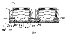
アレイ撮像モジュールは、支持部材、少なくとも1つの回路基板、少なくとも2つの感光ユニット、少なくとも2本のリード線、及びモールドシーラーを含む成形感光性アセンブリを含む。感光ユニットは、回路基板のチップ結合領域で結合される。リード線は、回路基板のチップ結合領域で感光ユニットに電気的に接続される。モールドシーラーは、モールド本体を含み、2つの光学ウィンドウを有する。モールド本体が形成されるとき、リード線、回路基板、及び感光ユニットは、モールドシーラーのモールド本体によって密封され、成形され、これによりモールド本体が形成された後、モールド本体及び回路基板の少なくとも一部分は、感光ユニットが、それぞれ光学ウィンドウと位置合わせされる、位置でともに一体化して形成される。
【選択図】図24
The arrayed imaging module includes a molded photosensitive assembly including a support member, at least one circuit board, at least two photosensitive units, at least two leads, and a mold sealer. The photosensitive units are coupled at the chip coupling area of the circuit board. The lead wire is electrically connected to the photosensitive unit in the chip coupling area of the circuit board. The mold sealer includes a mold body and has two optical windows. When the mold body is formed, the lead wire, the circuit board, and the photosensitive unit are sealed and molded by the mold body of the mold sealer, thereby forming at least a portion of the mold body and the circuit board. Photosensitive units are integrally formed together at locations, each aligned with an optical window.
[Selected figure] Figure 24
Description
本発明は、カメラモジュールに関し、より詳細にはアレイ撮像モジュール及びその成形感光性アセンブリ、並びに電子機器向けのその製造方法に関する。 The present invention relates to camera modules, and more particularly to array imaging modules and their shaped photosensitive assemblies, and methods of making the same for electronic devices.
今日では、電子製品の大部分は、1つの単一の電子部品で複数の機能を提供するために集積回路基板と合体している。特に、この統合された多機能がトレンド間で領域を超えることに留意されたい。例えば、元々は通信目的で設計される携帯電話の回路基板の構成は、一体的に集積回路と合体して通信、画像キャプチャ、インターネットへの接続が可能なアクセス、ナビゲーション、及び他の機能の複数の機能を提供する、スマートフォン等のモバイル電子機器に発展してきた。したがって、集積回路基板はスマートフォンに一体化した多機能を提供しなければならない。 Nowadays, the majority of electronic products are integrated with integrated circuit substrates to provide multiple functions in one single electronic component. In particular, it should be noted that this integrated multifunction crosses the area between trends. For example, the circuit board configuration of a cellular phone, originally designed for communication purposes, is integrated with integrated circuits to integrate communication, image capture, access to the Internet, access, navigation, and other functions. Has developed into mobile electronic devices such as smartphones, which provide the Thus, the integrated circuit board must provide multiple functions integrated into the smartphone.
したがって、現在のモバイル電子機器の大部分のカメラモジュールは、単レンズモジュールである。しかしながら、この単レンズカメラモジュールは、現在のモバイル電子機器の多機能用途の要件を満たすために高画像品質及びキャプチャ効果の要件を満たすことはできない。 Thus, most camera modules of current mobile electronic devices are single lens modules. However, this single lens camera module can not meet the requirements of high image quality and capture effects to meet the requirements of current mobile electronic device multifunctional applications.
二重レンズカメラモジュール等の高度カメラモジュールは、現在のモバイル電子機器ですでに使用されており、二重レンズカメラモジュールは、画像キャプチャのために人間の目の構造をシミュレーションするように構成されている。特に、3Dキャプチャ走査能力、ジェスチャ及び位置認識、色忠実度(色精度又はカラーバランス)、高速ピント合わせ能力、パノラマ撮影、背景被写界深度、及び他の態様等の二重レンズカメラモジュールの特徴及び性能は、単レンズカメラモジュールの特徴及び性能よりも優れている。したがって、将来のカメラ業界において、2つ以上のレンズのカメラモジュールを含めるための重要な開発方向がある。その結果、二重レンズカメラモジュールは概して2つの撮像モジュールを含み、これにより二重レンズカメラモジュールの2つの撮像キャプチャプロセスの間、2つの画像がそれぞれ撮像モジュールによってキャプチャされる。2つの撮像モジュール間の位置の相違のため、2つの画像は空間位置の差を有する。次いで、2つの画像は、最終的なキャプチャ画像を形成するために撮像合成方法によって処理される。撮像モジュールが、例えば解像度、シェーディング、色、及び水平方向、垂直方向、及び長手方向での偏差等の撮像効果の統一性を有さなければならないことが重要であり、これらの必要とされるものは、二重レンズカメラモジュールの画質を決定するための主要な要因である。 Advanced camera modules such as dual lens camera modules are already used in current mobile electronic devices, and dual lens camera modules are configured to simulate human eye structure for image capture There is. In particular, features of the dual lens camera module such as 3D capture scanning capability, gesture and position recognition, color fidelity (color accuracy or color balance), high speed focusing capability, panoramic photography, background depth of field, and other aspects And performance is superior to the features and performance of single lens camera modules. Thus, in the future camera industry, there is an important development direction to include camera modules of two or more lenses. As a result, the dual lens camera module generally includes two imaging modules, whereby two images are respectively captured by the imaging module during two imaging capture processes of the dual lens camera module. Due to the difference in position between the two imaging modules, the two images have differences in spatial position. The two images are then processed by the imaging compositing method to form the final captured image. It is important that the imaging module must have uniformity of imaging effects such as resolution, shading, color, and deviation in horizontal, vertical and longitudinal directions, these are needed Is the main factor to determine the image quality of the dual lens camera module.
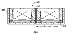
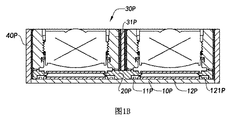
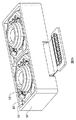
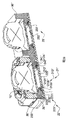
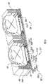
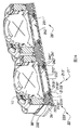
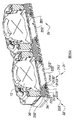
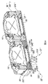
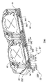
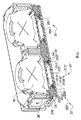
しかしながら、二重レンズカメラモジュールの現在の製造技術及び組立て技術、並びに構造は、その撮像品質を保証できない。図1に示されるように、既存の二重レンズカメラモジュールは、回路基板10P、2つのレンズベース20P、2つの撮像モジュール30P、及び1つの支持フレーム40Pを含み、レンズモータアセンブリ31Pは、撮像モジュール30Pのそれぞれに動作可能に接続される。したがって、レンズベース20Pのそれぞれは、回路基板10Pを介してレンズベース20Pを互いに接続するためにその片側で回路基板10Pに個別的に取り付けられる。レンズモータアセンブリ31Pは、対応するレンズベース20Pで結合され、対応するレンズベース20Pにより支持される。レンズモータアセンブリ31Pのそれぞれは、支持フレーム40Pにより包まれる。図1Bに示されるように、2つのレンズベース20Pは互いと統合されて、既存の技術に係る二重レンズカメラモジュールの単一のベースを形成できる。言い換えると、レンズモータアセンブリ31Pは、レンズベース20Pの異なる位置に取り付けられる。既存の二重レンズカメラモジュールの既存の組立てプロセスを通して、レンズベース20Pのそれぞれは、回路基板10Pで個々に結合され、これによりレンズベース20Pのそれぞれの寸法、位置等…は、制御するのが困難であることが理解される。言い換えると、二重レンズカメラモジュールの寸法及び組立て位置等のパラメータは変わりやすい。既存の二重レンズカメラモジュールによれば、レンズベース20Pは、図1Aに示されるように個々の構成要素であり、レンズベース20Pを互いと結合するために回路基板10Pに電気的に結合される。したがって、回路基板10PはPCB回路基板であり、回路基板10Pの剛性は相対的に弱く、これにより回路基板10Pは変形しやすい、又は曲がりやすい。結果として、二重レンズカメラモジュールの全体的な剛性は、制御し、保証するのが困難である。二重レンズカメラモジュールが組み立てられた後、二重レンズカメラモジュールの動作中、2つの撮像モジュール30Pの間には偏差がある。例えば、レンズモータアセンブリ31Pの間の距離は保証できず、レンズモータアセンブリ31Pの位置決め公差は相対的に大きく、撮像モジュール30Pのそれぞれの光軸は、その最初の事前に設定された位置から容易に逸脱する。これらの状況のうちのいずれか1つは、二重レンズカメラモジュールの画質に影響を及ぼす。例えば、制御不可能な要因及び悪影響が、最終的なキャプチャ画像を形成するための撮像合成プロセスに影響を及ぼす。さらに、レンズモータアセンブリ31Pは、支持フレーム40Pの中に包まれるので、レンズモータアセンブリ31Pと支持フレーム40Pとの間の隙間に接着剤を塗布することが必要である。結果として、二重レンズカメラモジュールの全体的なサイズは、さらに相対的に拡大される。
However, the current manufacturing technology and assembly technology of double-lens camera modules and the structure can not guarantee its imaging quality. As shown in FIG. 1, the existing double lens camera module includes a
さらに、二重レンズカメラモジュールの組立ては、従来のCOB(チップオンボード)組立てプロセスに基づく。回路基板10Pは、概して例えば金線121P等の接続線を介して回路基板10P上で電気的に結合された回路突出部11P及び感光性チップ12Pを含む。したがって、金線121Pは、回路基板の基板本体から突出した円弧の形状を有し、これにより回路基板10Pから突出した回路突出部11P及び金線121Pは、二重レンズカメラモジュールの組立てプロセスに悪影響を及ぼす。
Furthermore, the assembly of the dual lens camera module is based on the conventional COB (chip on board) assembly process. The
回路突出部11P及び金線121Pは、回路基板10Pから突出し、曝露されるので、組立てプロセスが、これらの曝露する構成要素によって影響を及ぼされるのは不可避である。例えば、レンズベース20Pの接着プロセス及びレンズモータアセンブリ31Pの溶接プロセスは、回路突出部11P及び金線121Pによって影響を及ぼされる。したがって、溶接抵抗剤(welding resisting agent)及び埃が、レンズモータアセンブリ31Pの溶接プロセスの間にレンズベース20Pに付着する場合がある。回路突出部11P及び感光性チップ12Pは、その間に隙間を生じさせるために位置決めされるので、埃はその隙間に蓄積する。埃は感光性チップ12Pを汚染し、これにより感光性チップ12Pは、例えば黒点等の望ましくない結果を生じさせて画質に影響を及ぼす。
Since the
さらに、レンズベース20Pは、回路突出部11Pの外部側に位置する。レンズベース20Pが、回路基板10Pに取り付けられるとき、レンズベース20Pと回路突出部11Pとの間には安全間隙が設けられなければならない。特に、安全間隙は、回路基板10Pに関してレンズベース20Pの水平方向及び上方向を含む。結果として、二重レンズカメラモジュールの厚さは、実質的に増加する。言い換えると、二重レンズカメラモジュールの全体的な厚さを削減することはほぼ不可能である。
Furthermore, the
また、二重レンズカメラモジュールの成形を単レンズカメラモジュールの成形と比較すると、二重レンズカメラの配位は、単レンズカメラモジュールの配位よりも高い。例えば、撮像モジュールの光軸は、同じ場所にあることが必要とされ、従来のCOBを通るレンズの光軸は一貫性がなければならない。まとめると、二重レンズカメラの全体的なサイズは相対的に大きく、回路基板の剛性は相対的に弱く、回路基板の平坦度は相対的に敏感であり、回路基板の厚さは相対的に大きい。 Also, when comparing the molding of a dual lens camera module with the molding of a single lens camera module, the configuration of the dual lens camera is higher than that of the single lens camera module. For example, the optical axes of the imaging modules need to be at the same location, and the optical axes of the lenses through the conventional COB must be consistent. In summary, the overall size of the dual lens camera is relatively large, the stiffness of the circuit board is relatively weak, the flatness of the circuit board is relatively sensitive, and the thickness of the circuit board is relatively large.
本発明は、それが電子機器用のアレイ撮像モジュール及びその成形感光性アセンブリ及び製造方法を提供するという点で有利であり、成形感光性アセンブリは、モールドシーラー及び感光装置を含み、感光装置は回路基板を含み、回路基板に電気的に接続される少なくとも2つの感光ユニットは、統合された構造を形成するためにモールドシーラーによって密封される。 The present invention is advantageous in that it provides an array imaging module for electronic devices and a shaped photosensitive assembly and method thereof, wherein the shaped photosensitive assembly comprises a mold sealer and a photosensitive device, the photosensitive device being a circuit At least two photosensitive units, including the substrate and electrically connected to the circuit board, are sealed by a mold sealer to form an integrated structure.
本発明の別の優位点は、電子機器向けのアレイ撮像モジュール及び成形感光性アセンブリ及び製造方法であり、感光ユニットは、1本以上のリード線を介して回路基板に電気的に接続され、リード線はモールドシーラーによって封入され、密封される。 Another advantage of the present invention is an array imaging module for electronic devices and a shaped photosensitive assembly and method of manufacture, wherein the photosensitive unit is electrically connected to the circuit board through one or more leads and leads The wire is enclosed and sealed by the mold sealer.
本発明の別の優位点は、電子機器向けのアレイ撮像モジュール及びその成形感光性アセンブリ及び製造方法であり、モールドシーラーは感光ユニットの非感光領域から広がり、モールドシーラーの周辺部サイズを最小限に抑えるために、感光ユニットの感光領域に向かって内向きに広がる。 Another advantage of the present invention is an array imaging module for electronic devices and its shaped photosensitive assembly and method of manufacture, wherein the mold sealer extends from the non-light sensitive area of the photosensitive unit and minimizes the size of the mold sealer perimeter It spreads inward towards the light sensitive area of the light sensitive unit in order to hold back.
本発明の別の優位点は、電子機器向けのアレイ撮像モジュール及びその成形感光性アセンブリ及び製造方法であり、感光装置は、回路基板から突出した少なくとも1つの電子的要素を含み、電子的要素は、電子的要素の外部への曝露を防ぐためにモールドシーラーによって封入される。 Another advantage of the present invention is an array imaging module for electronic devices and its shaped photosensitive assembly and method of manufacture, wherein the photosensitive device comprises at least one electronic element protruding from the circuit board, the electronic element being Sealed by a mold sealer to prevent external exposure of the electronic components.
本発明の別の優位点は、電子機器向けのアレイ撮像モジュール及びその成形感光性アセンブリ及び製造方法であり、モールドシーラーは、追加の支持体なしに複数の光フィルタを支持するために光フィルタ取付け部分を含む。 Another advantage of the present invention is an array imaging module for electronics and its shaped photosensitive assembly and method of manufacture, wherein the mold sealer mounts an optical filter to support multiple optical filters without additional support. Including parts.
本発明の別の優位点は、電子機器向けのアレイ撮像モジュール及びその成形感光性アセンブリ及び製造方法であり、モールドシーラーは、感光ユニットと係合するために複数の内側圧入溝を有し、これにより回路基板と感光ユニットの間の相対的な高さの差は、アレイ撮像モジュールの高さを最小限に抑えるために削減される。 Another advantage of the present invention is an array imaging module for electronic devices and its shaped photosensitive assembly and method of manufacture, wherein the mold sealer has a plurality of inner press fit grooves for engaging with the photosensitive unit, The relative height difference between the circuit board and the photosensitive unit is thereby reduced to minimize the height of the array imaging module.
本発明の別の優位点は、電子機器向けのアレイ撮像モジュール及びその成形感光性アセンブリ及び製造方法であり、回路基板は、複数の導電性チャネル、及び対応してそれと形成された複数の外側のインデント溝を含み、これにより感光ユニットは、フリップチップ(FC)方法によって回路基板の裏面で結合できる。 Another advantage of the present invention is an array imaging module for electronic devices and its shaped photosensitive assembly and method of manufacture, wherein the circuit board comprises a plurality of conductive channels and a plurality of outer correspondingly formed therewith. Indentation grooves are included so that the photosensitive units can be bonded on the back side of the circuit board by a flip chip (FC) method.
本発明の別の優位点は、電子機器向けのアレイ撮像モジュール及びその成形感光性アセンブリ及び製造方法であり、補強層は、回路基板の強度を補強するためだけではなく、回路基板の放熱を強化するためにも回路基板の底面で結合される。 Another advantage of the present invention is an array imaging module for electronic devices and its shaped photosensitive assembly and method of manufacture, wherein the reinforcing layer not only enhances the strength of the circuit board but also enhances the heat dissipation of the circuit board To be bonded at the bottom of the circuit board.
本発明の別の優位点は、電子機器向けのアレイ撮像モジュール及びその成形感光性アセンブリ及び製造方法であり、回路基板はその上に少なくとも1つの補強長穴をさらに含み、モールドシーラーは回路基板の強度を高めるために補強長穴の中に広がる。 Another advantage of the present invention is an array imaging module for electronic devices and its shaped photosensitive assembly and method of manufacture, wherein the circuit board further comprises at least one reinforced elongated hole thereon and the mold sealer is of the circuit board Expand into the reinforcing slot to increase strength.
本発明の別の優位点は、電子機器向けのアレイ撮像モジュール及びその成形感光性アセンブリ及び製造方法であり、モールドシーラーは、それぞれの光フィルタを適所に保持するために、複数の光フィルタを支持する光フィルタ取付け部分を含む。 Another advantage of the present invention is an array imaging module for electronics and its shaped photosensitive assembly and method of manufacture, wherein the mold sealer supports a plurality of light filters to hold the respective light filters in place. Optical filter mounting portion.
本発明の別の優位点は、電子機器向けのアレイ撮像モジュール及びその成形感光性アセンブリ及び製造方法であり、成形感光性アセンブリは、リード線を損傷又は変形されることから保護するために、成形プロセスの間、上部モールド本体の係合面に対して偏向する少なくとも1つの支持部材を含む。 Another advantage of the present invention is an array imaging module for electronic devices and its shaped photosensitive assembly and method of manufacture, wherein the shaped photosensitive assembly is molded to protect the leads from being damaged or deformed The process includes at least one support member that biases against the engagement surface of the upper mold body during the process.
本発明の別の優位点は、電子機器向けのアレイ撮像モジュール及びその成形感光性アセンブリ及び製造方法であり、モールドの上部モールド本体及び下部モールド本体が、成形プロセスの間、閉じられ、互いと係合されるとき、支持部材は、上部モールド本体の係合面に対して偏向して、上部モールド本体の係合面がリード線と接触するのを防いでリード線の変形を防ぐために上方に伸ばされる。 Another advantage of the present invention is an array imaging module for electronics and its molded photosensitive assembly and method of manufacture, wherein the upper and lower mold bodies of the mold are closed and engaged with each other during the molding process When mated, the support member is biased against the engagement surface of the upper mold body to extend upward to prevent the engagement surface of the upper mold body from contacting the lead and to prevent deformation of the lead. Be
本発明の別の優位点は、電子機器向けのアレイ撮像モジュール及びその成形感光性アセンブリ及び製造方法であり、モールドの上部モールド本体及び下部モールド本体が、成形プロセスの間に閉じられ、互いと係合されるとき、支持部材は、上部モールド本体の係合面がリード線を圧迫するのを防ぐためにリード線の安全距離を提供する。 Another advantage of the present invention is an array imaging module for electronics and its molded photosensitive assembly and method of manufacture, wherein the upper and lower mold bodies of the mold are closed during the molding process and interlocked with each other When mated, the support member provides a safe distance for the lead to prevent the engagement surface of the upper mold body from squeezing the lead.
本発明の別の優位点は、電子機器向けのアレイ撮像モジュール及びその成形感光性アセンブリ及び製造方法であり、モールドの上部モールド本体及び下部モールド本体が、成形プロセスの間に閉じられ、互いと係合されるとき、支持部材は、感光ユニット、回路基板、及びリード線の損傷を防ぐために上部モールド本体の係合面の衝撃力を吸収する。 Another advantage of the present invention is an array imaging module for electronics and its molded photosensitive assembly and method of manufacture, wherein the upper and lower mold bodies of the mold are closed during the molding process and interlocked with each other When mated, the support member absorbs the impact force of the engagement surface of the upper mold body to prevent damage to the photosensitive unit, the circuit board, and the leads.
本発明の別の優位点は、電子機器向けのアレイ撮像モジュール及びその成形感光性アセンブリ及び製造方法であり、モールドの上部モールド本体及び下部モールド本体が、成形プロセスの間に閉じられ、互いと係合されるとき、上部モールド本体のモールド係合面及び支持体の上面は、表面対表面の係合方法で互いとしっかりと係合されて、アレイ撮像モジュールの撮像品質を高めるためにモールドシーラーの端縁トリミングを防ぐ。 Another advantage of the present invention is an array imaging module for electronics and its molded photosensitive assembly and method of manufacture, wherein the upper and lower mold bodies of the mold are closed during the molding process and interlocked with each other When mated, the mold engaging surface of the upper mold body and the upper surface of the support are firmly engaged with each other in a surface to surface engaging manner to enhance the imaging quality of the array imaging module Prevent edge trimming.
本発明の別の優位点は、電子機器向けのアレイ撮像モジュール及びその成形感光性アセンブリ及び製造方法であり、モールドの上部モールド本体及び下部モールド本体が、閉じられ、互いと係合されるとき、上部モールド本体のモールド係合面及び支持体の上面は、モールド材料が閉環境の中に進入して、感光ユニットの感光領域を汚染するのを防ぐように、互いとしっかりと係合されて、成形プロセスの間に閉環境を形成する。 Another advantage of the present invention is an array imaging module for electronics and its shaped photosensitive assembly and method of manufacture, wherein the upper and lower mold bodies of the mold are closed and engaged with one another, The mold engaging surface of the upper mold body and the upper surface of the support are firmly engaged with each other to prevent mold material from entering the closed environment and contaminating the light sensitive area of the photosensitive unit. Form a closed environment during the molding process.
本発明の別の優位点は、電子機器向けのアレイ撮像モジュール及びその成形感光性アセンブリ及び製造方法であり、モールドは、上部モールド本体のモールド係合面に設けられた封入膜を含み、上部モールド本体及び下部モールド本体が互いと結合されるとき、封入膜は、感光ユニット、回路基板、及びリード線の損傷を防ぐために、上部モールド本体のモールド係合面と支持体の上面との間に挟まれる。 Another advantage of the present invention is an array imaging module for electronic devices and its molded photosensitive assembly and method of manufacture, wherein the mold includes an encapsulation film provided on the mold engaging surface of the upper mold body, and the upper mold When the body and lower mold body are coupled to each other, the encapsulation film is sandwiched between the mold engaging surface of the upper mold body and the top surface of the support to prevent damage to the photosensitive unit, the circuit board, and the leads. Be
本発明の別の優位点は、電子機器向けのアレイ撮像モジュール及びその成形感光性アセンブリ及び製造方法であり、上部モールド本体及び下部モールド本体が互いと結合されるとき、封入膜は、モールド材料が閉環境に進入して、感光ユニットの感光領域を汚染するのを防ぐように、上部モールド本体のモールド係合面と支持体の上面との間に挟まれて閉環境に感光ユニットの感光領域を形成する。 Another advantage of the present invention is an array imaging module for electronic devices and its shaped photosensitive assembly and method of manufacture, wherein when the upper mold body and the lower mold body are combined with each other, the encapsulation film is a molding material In order to prevent entering the closed environment and contaminating the photosensitive area of the photosensitive unit, the photosensitive area of the photosensitive unit is exposed to the closed environment by being sandwiched between the mold engaging surface of the upper mold body and the upper surface of the support. Form.
本発明の別の優位点は、電子機器向けのアレイ撮像モジュール及びその成形感光性アセンブリ及び製造方法であり、上部モールド本体のモールド係合面が支持体の上面に対して偏向されるとき、支持部材は、リード線の変形を防いでリード線の電気伝導性を維持するために変形されない。 Another advantage of the present invention is an array imaging module for electronic devices and its shaped photosensitive assembly and method of manufacture, wherein the support when the mold engaging surface of the upper mold body is deflected against the upper surface of the support The member is not deformed to prevent deformation of the lead and maintain electrical conductivity of the lead.
本発明の別の優位点は、電子機器向けのアレイ撮像モジュール及びその成形感光性アセンブリ及び製造方法であり、支持部材は伸ばされて、感光ユニットの非感光領域の少なくとも一部分を封入し、モールド材料が感光ユニットの非感光領域から感光ユニットの感光領域に進入するのを阻止して感光ユニットの感光領域の汚染を防ぐ。 Another advantage of the present invention is an arrayed imaging module for electronic devices and its shaped photosensitive assembly and method of manufacture, wherein the support member is stretched to encapsulate at least a portion of the non-photosensitive area of the photosensitive unit, and the molding material Prevents the contamination of the photosensitive area of the photosensitive unit by preventing it from entering the photosensitive area of the photosensitive unit from the non-photosensitive area of the photosensitive unit.
本発明の別の優位点は、電子機器向けのアレイ撮像モジュール及びその成形感光性アセンブリ及び製造方法であり、支持部材は、感光ユニットのチップコネクタと回路基板の回路コネクタとの間の接続部を封入するように構成され、これにより成形プロセスの間、支持部材は、感光ユニットと回路基板との間の電気接続の信頼性を高めるために、接続に入るためのモールド材料を阻止する。 Another advantage of the present invention is an array imaging module for electronic devices and its shaped photosensitive assembly and method of manufacture, wherein the support member is a connection between the chip connector of the photosensitive unit and the circuit connector of the circuit board. It is configured to encapsulate, whereby the support member blocks the mold material to enter the connection in order to enhance the reliability of the electrical connection between the photosensitive unit and the circuit board during the molding process.
本発明の別の優位点は、電子機器向けのアレイ撮像モジュール及びその成形感光性アセンブリ及び製造方法であり、支持部材は、モールド材料のリード線に対する衝撃力を妨げるために、成形プロセスの間、回路基板の周辺部分の少なくとも一部分を封入する。 Another advantage of the present invention is an array imaging module for electronics and its shaped photosensitive assembly and method of manufacture, wherein the support member is used during the molding process to prevent impact forces on the leads of the molding material. At least a portion of the peripheral portion of the circuit board is enclosed.
本発明の別の優位点は、電子機器向けのアレイ撮像モジュール及びその成形感光性アセンブリ及び製造方法であり、支持部材は、回路基板の周辺部分の少なくとも一部分を封入し、感光ユニットの感光領域から離れて位置し、これにより支持フレームの形成中、支持フレームは、感光ユニットの任意の暗い点を防ぐために感光ユニットの感光領域を汚染しない。 Another advantage of the present invention is an array imaging module for electronic devices and its shaped photosensitive assembly and method of manufacture, wherein the support member encapsulates at least a portion of the peripheral portion of the circuit board and from the photosensitive area of the photosensitive unit Located apart, and thereby forming the support frame, the support frame does not contaminate the light sensitive areas of the light sensitive unit to prevent any dark spots of the light sensitive unit.
本発明の別の優位点は、電子機器向けのアレイ撮像モジュール及びその成形感光性アセンブリ及び製造方法であり、支持部材は、回路基板及び感光ユニットを確実に保持するために、回路基板の周辺部分の少なくとも一部分及び感光ユニットの非感光領域の少なくとも一部分を封入する。したがって、上部モールド本体及び下部モールド本体が互いと結合されて、その間にモールド空洞を形成するとき、支持部材は、その変位を妨げるために回路基板及び感光ユニットを保持できる。 Another advantage of the present invention is an array imaging module for electronic devices and its shaped photosensitive assembly and method of manufacture, wherein the support member is a peripheral portion of the circuit board to securely hold the circuit board and the photosensitive unit. And at least a portion of the light insensitive areas of the light sensitive unit. Thus, when the upper mold body and the lower mold body are coupled to one another to form a mold cavity therebetween, the support member can hold the circuit board and the photosensitive unit to prevent its displacement.
本発明の別の優位点は、電子機器向けのアレイ撮像モジュール及びその成形感光性アセンブリ及び製造方法であり、支持部材は、回路基板の周辺部分の少なくとも一部分及び感光ユニットの非感光領域の少なくとも一部分を封入し、これにより成形プロセスの間、支持部材は、感光ユニットと回路基板との間の間隙に進入するモールド材料を阻止できる。 Another advantage of the present invention is an array imaging module for electronic devices and its shaped photosensitive assembly and method of manufacture, wherein the support member comprises at least a portion of the peripheral portion of the circuit board and at least a portion of the non-photosensitive area of the photosensitive unit. And the support member can block mold material entering the gap between the photosensitive unit and the circuit board during the molding process.
本発明の別の優位点は、電子機器向けのアレイ撮像モジュール及びその成形感光性アセンブリ及び製造方法であり、支持部材は、リード線のそれぞれの少なくとも一部分を封入し、これにより成形プロセスの間、リード線は、リード線の電気伝導性を維持するために支持部材によって保護される。 Another advantage of the present invention is an array imaging module for electronic devices and its shaped photosensitive assembly and method of manufacture, wherein the support member encapsulates at least a portion of each of the leads, thereby during the molding process The lead is protected by the support member to maintain the electrical conductivity of the lead.
本発明の別の優位点は、電子機器向けのアレイ撮像モジュール及びその成形感光性アセンブリ及び製造方法であり、支持部材は、リード線のそれぞれの少なくとも一部分を封入し、これによりアレイ撮像モジュールの動作中、アレイ撮像モジュールの撮像品質を高めるために、迷光がアレイ撮像モジュールの内部に進入するのを防ぐことができる。 Another advantage of the present invention is an array imaging module for electronic devices and its shaped photosensitive assembly and method of manufacture, wherein the support member encapsulates at least a portion of each of the leads, thereby operating the array imaging module In order to improve the imaging quality of the array imaging module, it is possible to prevent stray light from entering the inside of the array imaging module.
本発明の別の優位点は、電子機器向けのアレイ撮像モジュール及びその成形感光性アセンブリ及び製造方法であり、支持部材は、感光ユニットの感光領域の汚染を防ぐために、電子的要素の溶接プロセスの間に、溶接粉等の汚染物を付着させる所定の付着能を有する。 Another advantage of the present invention is an array imaging module for electronic devices and its shaped photosensitive assembly and method of manufacture, wherein the support member is for the process of welding electronic elements to prevent contamination of the photosensitive area of the photosensitive unit. In the meantime, it has a predetermined adhesion ability to attach contaminants such as weld powder.
本発明の別の優位点は、電子機器向けのアレイ撮像モジュール及びその成形感光性アセンブリ及び製造方法であり、支持部材の上面は、感光ユニットのチップコネクタの上面の上方に位置して、成形プロセスの間の感光ユニットのチップコネクタの損傷を防ぐ。 Another advantage of the present invention is an array imaging module for electronic devices and its shaped photosensitive assembly and method of manufacture, wherein the upper surface of the support member is located above the upper surface of the chip connector of the photosensitive unit, the forming process Prevent damage to the tip connector of the photosensitive unit during the
本発明の別の優位点は、電子機器向けのアレイ撮像モジュール及びその成形感光性アセンブリ及び製造方法であり、支持部材は、感光ユニットのチップコネクタを封入し、これにより成形プロセスの間、支持部材は、感光ユニットのチップコネクタを保護するために、モールド材料が、感光ユニットのチップコネクタに進入する又は感光ユニットのチップコネクタで封入するのを阻止する。 Another advantage of the present invention is an array imaging module for electronic devices and its shaped photosensitive assembly and method of manufacture, wherein the support member encapsulates the chip connector of the photosensitive unit, thereby supporting the support member during the molding process. In order to protect the chip connector of the photosensitive unit, the molding material is prevented from entering the chip connector of the photosensitive unit or being sealed with the chip connector of the photosensitive unit.
本発明の別の優位点は、電子機器向けのアレイ撮像モジュール及びその成形感光性アセンブリ及び製造方法であり、支持部材は、感光ユニットのチップコネクタの外側部分に形成されて、モールド材料が、成形プロセスの間、感光ユニットのチップコネクタと接触するのを防ぐ。言い換えると、支持部材は、感光ユニットのチップコネクタを保護するために、モールド材料が、感光ユニットのチップコネクタに進入する又は感光ユニットのチップコネクタで封入するのを阻止する。 Another advantage of the present invention is an array imaging module for electronic devices and its shaped photosensitive assembly and method of manufacture, wherein the support member is formed on the outer part of the chip connector of the photosensitive unit and the molding material is molded Prevent contact with the tip connector of the photosensitive unit during the process. In other words, the support member prevents the mold material from entering the chip connector of the photosensitive unit or encapsulating it in the chip connector of the photosensitive unit in order to protect the chip connector of the photosensitive unit.
本発明の別の優位点は、電子機器向けのアレイ撮像モジュール及びその成形感光性アセンブリ及び製造方法であり、支持物は、それぞれドライバと同軸上で位置合わせされるための光学レンズを保証するためのドライバ又は支持部材と結合するために少なくとも2つの支持空洞を有する。 Another advantage of the present invention is an array imaging module for electronic devices and its shaped photosensitive assembly and method of manufacture, wherein the supports each guarantee an optical lens to be coaxially aligned with the driver And at least two support cavities for coupling with the driver or support member of the
本発明の別の優位点は、電子機器向けのアレイ撮像モジュール及び成形感光性アセンブリ及び製造方法であり、光フィルタは、アレイ撮像モジュールの撮像品質を高めるためのアレイ撮像モジュールの内部に進入する光を保証するために、各感光ユニットと、光学レンズから迷光を除外するための各光学レンズとの間に保持される。 Another advantage of the present invention is an array imaging module and shaped photosensitive assembly and manufacturing method for electronic devices, wherein the light filter enters the inside of the array imaging module to enhance the imaging quality of the array imaging module Are held between each photosensitive unit and each optical lens for eliminating stray light from the optical lens.
本発明の追加の優位点及び特徴は、続く説明から明らかになり、添付の特許請求の範囲に特に指摘される手段及び組合せによって実現されてよい。 Additional advantages and features of the present invention will be apparent from the ensuing description and may be realized by means and combinations particularly pointed out in the appended claims.
本発明によれば、上記の及び他の目的及び優位点は、
モールドシーラーと、
回路基板で電気的に結合された少なくとも1つの回路基板及び少なくとも2つの感光ユニットを含む感光装置であって、回路基板及び感光性ユニットは、モールドシーラーによって密封されて一体集積機器を形成する、感光装置と
を含む、アレイ撮像モジュールの成形感光性アセンブリによって達成される。
According to the invention, the above and other objects and advantages are:
Mold sealer,
A photosensitive device comprising at least one circuit board electrically coupled with a circuit board and at least two photosensitive units, the circuit board and the photosensitive unit being sealed by a mold sealer to form an integral integrated device And a device, which is achieved by a shaped photosensitive assembly of the array imaging module.
一実施形態では、モールドシーラーは、それぞれ感光ユニットのために2つの光チャネルを形成するために、感光ユニットと位置合わせされた2つの光学ウィンドウを有する。 In one embodiment, the mold sealer has two optical windows aligned with the photosensitive unit to respectively form two light channels for the photosensitive unit.
一実施形態では、モールドシーラーの光学ウィンドウのそれぞれは、光学ウィンドウの断面が下から上に徐々に拡大する先細サイズを有するように構成される。 In one embodiment, each of the mold sealer's optical windows is configured to have a tapered size in which the cross section of the optical window gradually expands from bottom to top.
一実施形態では、モールドシーラーの上面は、支持物、光学レンズ、ドライバ、又は光フィルタを支持するために配置される。 In one embodiment, the top surface of the mold sealer is arranged to support a support, an optical lens, a driver or a light filter.
一実施形態では、モールドシーラーは、その上面に形成され、支持物、光学レンズ、ドライバ、又は光フィルタと係合するために光学ウィンドウに対応して広がる少なくとも1つの結合長穴をさらに有する。 In one embodiment, the mold sealer further comprises at least one coupling slot formed in the upper surface thereof and extending correspondingly to the optical window for engaging a support, an optical lens, a driver or an optical filter.
一実施形態では、モールドシーラーは、封入部分、光フィルタ取付け部分、及びレンズ取付け部分を有し、光フィルタ取付け部分及びレンズ取付け部分は、封入部分から一体化して且つ上方に広がって、光フィルタ及び光学レンズを適所に間隔をおいて支持するために階段状のプラットフォームを形成する。 In one embodiment, the mold sealer includes an encapsulation portion, an optical filter attachment portion, and a lens attachment portion, the optical filter attachment portion and the lens attachment portion integrally and upwardly extending from the encapsulation portion to form the optical filter and A step-like platform is formed to support the optical lenses in spaced apart positions.
一実施形態では、光フィルタ取付け部分は、そこで光フィルタを支持するように、階段状のプラットフォームの第1の段を形成するために光学ウィンドウに対応して位置する2つの取付け長穴を有する。レンズ取付け部分は、そこで光学レンズを支持するように、階段状のプラットフォームの第2の段を形成するために光学ウィンドウに対応して位置する2つのレンズ取付け長穴をさらに有する。 In one embodiment, the light filter mounting portion has two mounting slots located corresponding to the optical window to form a first step of the stepped platform to support the light filter therein. The lens mounting portion further comprises two lens mounting slots positioned corresponding to the optical window to form a second step of the stepped platform to support the optical lens there.
一実施形態では、レンズ取付け部分は、2つのレンズ内壁をさらに有し、レンズ内壁のそれぞれは、いかなるねじ構造もない光学レンズと結合するために平面である。 In one embodiment, the lens mounting portion further comprises two lens inner walls, each of the lens inner walls being planar for coupling with an optical lens without any screw structure.
一実施形態では、感光装置は、感光ユニット、回路基板と電気的に接続された少なくとも1本のリード線を含み、リード線は、リード線が外部に曝露されるのを防ぐためにモールドシーラーによって封入される。 In one embodiment, the photosensitive device includes a photosensitive unit, at least one lead electrically connected to the circuit board, and the lead is encapsulated by a mold sealer to prevent the lead from being exposed to the outside. Be done.
一実施形態では、リード線は、金線、銀線、銅線、又はアルミニウム線である場合がある。 In one embodiment, the lead may be a gold wire, a silver wire, a copper wire, or an aluminum wire.
一実施形態では、リード線は、感光ユニットと回路基板との間で電気的に接続するために曲線状の構成を有する。 In one embodiment, the lead has a curvilinear configuration to electrically connect between the photosensitive unit and the circuit board.
一実施形態では、各感光ユニットは、感光領域及び非感光領域を有し、感光領域は、非感光領域の中で取り囲まれている。モールドシーラーは、モールドシーラーの周辺サイズを最小限に抑えるために、非感光領域から感光領域に向かって内向きに広がる。 In one embodiment, each photosensitive unit comprises a photosensitive area and a non-photosensitive area, wherein the photosensitive area is enclosed within the non-photosensitive area. The mold sealer extends inwardly from the unexposed area towards the exposed area to minimize the peripheral size of the mold sealer.
一実施形態では、感光装置は、回路基板から突出する少なくとも1つの電子的要素を含み、モールドシーラーは、電子的要素が外部に曝露されるのを防ぐために電子的要素を封入する。 In one embodiment, the photosensitive device includes at least one electronic element protruding from the circuit board, and the mold sealer encloses the electronic element to prevent the electronic element from being exposed to the outside.
一実施形態では、電子的要素は、抵抗器、コンデンサ、ダイオード、三極管、ポテンショメータ、リレー、ドライバ、プロセッサ、又は上記の組合せである場合がある。 In one embodiment, the electronic component may be a resistor, a capacitor, a diode, a triode, a potentiometer, a relay, a driver, a processor, or a combination of the above.
一実施形態では、感光装置は、それぞれ感光ユニットをカバーする少なくとも2つの光フィルタを含み、モールドシーラーは、回路基板、感光ユニット、及び光フィルタを封入し、これにより感光ユニットのそれぞれは、アレイ撮像モジュールの焦点距離及び高さを削減するために各光フィルタによって保護される。 In one embodiment, the photosensitive device includes at least two light filters, each covering a photosensitive unit, and a mold sealer encloses the circuit board, the photosensitive unit, and the light filter, whereby each of the photosensitive units is an array imaging Protected by each optical filter to reduce module focal length and height.
一実施形態では、光学装置は、回路基板の強度を補強するために回路基板に重ね合わされ、接続された補強層をさらに含む。 In one embodiment, the optical device further includes a reinforcement layer superimposed and connected to the circuit board to reinforce the strength of the circuit board.
一実施形態では、補強層は、回路基板の放熱を強化するために金属パネルである。 In one embodiment, the reinforcing layer is a metal panel to enhance heat dissipation of the circuit board.
一実施形態では、感光装置は、回路基板の強度を高めるために、及び成形感光性アセンブリの任意の電磁干渉を防ぐために回路基板及びモールドシーラーを封入するシールド層をさらに含む。 In one embodiment, the photosensitive device further includes a shield layer encapsulating the circuit board and the mold sealer to increase the strength of the circuit board and to prevent any electromagnetic interference of the molded photosensitive assembly.
一実施形態では、シールド層は、金属パネル又は金属網である場合がある。 In one embodiment, the shield layer may be a metal panel or a metal mesh.
一実施形態では、感光装置は、少なくとも1つの補強長穴を有し、モールドシーラーは、回路基板の強度を高めるために補強長穴の中に広げられる。 In one embodiment, the photosensitive device has at least one reinforcing slot, and the mold sealer is extended into the reinforcing slot to increase the strength of the circuit board.
一実施形態では、補強長穴は、インデント空洞である。 In one embodiment, the reinforcement slots are indented cavities.
一実施形態では、補強長穴は貫通長穴であり、これによりモールドシーラーは、モールドシーラーを回路基板と結合するために、回路基板を通って広げられてその間の接触面積を最大にし、回路基板と一体化して形成する。さらに、貫通長穴としての補強長穴は、回路基板上に容易に形成できる。 In one embodiment, the reinforced elongated holes are through elongated holes so that the mold sealer is spread through the circuit board to maximize the contact area between the circuit boards in order to couple the mold sealer with the circuit board Integrated with Furthermore, the reinforcing elongated hole as the through elongated hole can be easily formed on the circuit board.
一実施形態では、回路基板は、硬軟結合基板(soft−hard combination board)、セラミック基板、ハードPCB基板、又はFPCである場合がある。 In one embodiment, the circuit board may be a soft-hard combination board, a ceramic board, a hard PCB board, or an FPC.
一実施形態では、モールドシーラーのモールド材料は、ナイロン、LCP(液晶ポリマー)、PP(ポリプロピレン)、又は上記の組合せである場合がある。 In one embodiment, the mold sealer mold material may be nylon, LCP (liquid crystal polymer), PP (polypropylene), or a combination of the above.
一実施形態では、成形感光性アセンブリは、少なくとも2つのモータ接続ユニットをさらに含み、モータ接続ユニットのそれぞれは、モールドシーラーに埋め込まれ、回路基板に電気的に接続された第1の接続線を有する。第1の接続線は、ドライバのドライバ接続端子に電気的に接続するためにモールドシーラーの上面上方に曝露され、伸ばされる第1のモータ接続端部を有する。 In one embodiment, the shaped photosensitive assembly further includes at least two motor connection units, each of the motor connection units having a first connection wire embedded in the mold sealer and electrically connected to the circuit board . The first connection line has a first motor connection end exposed and extended above the top surface of the mold sealer to electrically connect to the driver connection terminal of the driver.
一実施形態では、成形感光性アセンブリは、少なくとも2つのモータ接続ユニットをさらに含み、モータ接続ユニットのそれぞれは、少なくとも1本の接続線及び端子長穴を有する。接続線は、モールドシーラーに埋め込まれ、回路基板に電気的に接続される。モータ接続ユニットの第1の端子長穴は、モールドシーラーの上面に広がる。接続線は、モールドシーラーで設定され、端子長穴の底壁面に伸ばされる。接続線は、モールドシーラーに設けられ、端子長穴の底壁面に広がる第2のモータ接続端部を含み、第2のモータ接続端部は、ドライバのドライバ接続端子に電気的に結合される。 In one embodiment, the shaped photosensitive assembly further comprises at least two motor connection units, each of the motor connection units having at least one connection wire and a terminal slot. The connection lines are embedded in the mold sealer and electrically connected to the circuit board. The first terminal elongated hole of the motor connection unit extends to the upper surface of the mold sealer. The connection line is set by a mold sealer and extended to the bottom wall of the terminal long hole. The connection line is provided on the mold sealer and includes a second motor connection end that extends to the bottom wall of the terminal slot, and the second motor connection end is electrically coupled to the driver connection terminal of the driver.
一実施形態では、成形感光性アセンブリは、少なくとも2つのモータ接続ユニットをさらに含み、モータ接続ユニットのそれぞれは、少なくとも1つの端子長穴及び少なくとも1つの回路端子を有する。回路端子は、回路基板で事前に設定され、回路基板に電気的に接続される。端子長穴は、モールドシーラーに設けられ、回路基板からモールドシーラーの上面に広がる。回路端子は、ドライバのドライバ接続端子と接続するために端子長穴に対応して伸ばされる。 In one embodiment, the shaped photosensitive assembly further comprises at least two motor connection units, each of the motor connection units having at least one terminal slot and at least one circuit terminal. The circuit terminals are preset at the circuit board and electrically connected to the circuit board. The terminal elongated hole is provided in the mold sealer and extends from the circuit board to the top surface of the mold sealer. The circuit terminal is stretched corresponding to the terminal elongated hole to connect with the driver connection terminal of the driver.
一実施形態では、成形感光性アセンブリは、少なくとも2つのモータ接続ユニットをさらに含み、モータ接続ユニットのそれぞれは、回路基板に電気的に接続された少なくとも1つの彫刻(engraving)回路を有し、彫刻回路は、ドライバのドライバ接続端子と接続するためにモールドシーラーに埋め込まれる。 In one embodiment, the shaped photosensitive assembly further comprises at least two motor connection units, each of the motor connection units having at least one engraving circuit electrically connected to the circuit board, the engraving The circuit is embedded in the mold sealer to connect with the driver connection terminal of the driver.
一実施形態では、彫刻回路は、モールドシーラーに埋め込まれるために、レーザーダイレクトストラクチャリング(LDS)によって形成される。 In one embodiment, the engraving circuit is formed by laser direct structuring (LDS) to be embedded in a mold sealer.
本発明の別の態様によれば、本発明は、
モールドシーラーと、回路基板及び回路基板で電気的に結合された少なくとも2つの感光ユニットを含む感光装置とを含む成形感光性アセンブリであって、回路基板及び感光ユニットがモールドシーラーによって密封されて一体集積機器を形成する、感光性アセンブリと、
成形感光性アセンブリに結合され、それぞれ感光ユニットの2つの感光経路に沿って位置する少なくとも2つの光学レンズと
を含む、アレイ撮像モジュールを含む。
According to another aspect of the invention, the invention is
A molded photosensitive assembly including a mold sealer and a photosensitive device including a circuit board and at least two photosensitive units electrically connected by the circuit board, wherein the circuit board and the photosensitive unit are sealed by the mold sealer and integrally integrated. Photosensitive assembly, forming equipment
And an array imaging module including at least two optical lenses coupled to the shaped photosensitive assembly, each located along two photosensitive paths of the photosensitive unit.
一実施形態では、アレイ撮像モジュールは、感光ユニットで結合された支持物、及び支持物によって支持される少なくとも2つの光フィルタをさらに含む。 In one embodiment, the array imaging module further includes a support coupled at the photosensitive unit, and at least two light filters supported by the support.
一実施形態では、アレイ撮像モジュールは、それぞれ2つの光学レンズに動作可能なように結合された少なくとも2つのドライバをさらに含み、ドライバは、それぞれ感光ユニットに結合される。 In one embodiment, the array imaging module further comprises at least two drivers each operatively coupled to the two optical lenses, wherein the drivers are each coupled to the photosensitive unit.
一実施形態では、アレイ撮像モジュールは、それぞれ感光ユニットに結合された少なくとも2つの光フィルタをさらに含む。 In one embodiment, the array imaging module further comprises at least two light filters each coupled to the photosensitive unit.
一実施形態では、アレイ撮像モジュールは、モールドシーラーによってそれぞれ感光ユニットと一体化して形成された少なくとも2つの光フィルタをさらに含む。 In one embodiment, the array imaging module further includes at least two light filters formed integrally with the photosensitive unit by the mold sealer, respectively.
本発明の別の態様によれば、本発明は、アレイ撮像モジュールの成形感光性アセンブリの製造方法を含み、該製造方法は、モールドシーラーが、回路基板及び少なくとも2つの感光ユニットを一体化して封入し、実装し、密封するステップを含む。 According to another aspect of the present invention, the present invention includes a method of manufacturing a molded photosensitive assembly of an array imaging module, wherein the mold sealer integrally encapsulates a circuit board and at least two photosensitive units. , Mounting and sealing.
一実施形態では、成形ステップの前に、方法は、少なくとも1本のリード線を介して感光ユニットを回路基板に電気的に接続するステップをさらに含む。 In one embodiment, prior to the forming step, the method further comprises the step of electrically connecting the photosensitive unit to the circuit board via at least one lead.
一実施形態では、成形ステップは、モールドシーラーによってリード線を封入するステップをさらに含む。 In one embodiment, the forming step further comprises the step of encapsulating the lead with a mold sealer.
一実施形態では、成形ステップは、モールドシーラーを感光ユニットの非感光領域に広げるステップをさらに含む。 In one embodiment, the molding step further comprises the step of spreading the mold sealer over the light insensitive areas of the light sensitive unit.
一実施形態では、方法は、支持物、光学レンズ、ドライバ、又は光フィルタと係合するためにモールドシーラーの上面に少なくとも1つの結合長穴を形成するステップをさらに含む。 In one embodiment, the method further comprises the step of forming at least one coupling slot in the top surface of the mold sealer to engage with the support, optical lens, driver or light filter.
一実施形態では、方法は、光フィルタ及び光学レンズを適所に間隔をおいて支持するためにモールドシーラーの内側から上方に広がる階段状のプラットフォームを形成するステップをさらに含む。 In one embodiment, the method further includes the step of forming a stepped platform extending upwardly from the inside of the mold sealer to support the light filter and the optical lens in place.
一実施形態では、成形ステップは、対応するねじ構成を有する光学レンズと結合するためにモールドシーラーの内壁にねじ構造を形成するステップをさらに含む。 In one embodiment, the forming step further includes forming a threading on the inner wall of the mold sealer to couple with an optical lens having a corresponding threading configuration.
一実施形態では、成形ステップの前に、方法は、回路基板で、インデント空洞である少なくとも1つの補強長穴を形成するステップをさらに含み、モールドシーラーは、回路基板の強度を高めるために補強長穴の中に広がる。 In one embodiment, prior to the forming step, the method further includes forming at least one reinforced slot, which is an indented cavity, in the circuit board, the mold sealer including the reinforced length to enhance the strength of the circuit board. Spread in the hole.
一実施形態では、成形ステップの前に、方法は、回路基板で、貫通長穴である少なくとも1つの補強長穴を形成するステップをさらに含み、モールドシーラーは、回路基板の強度を高めるために補強長穴の中に広がる。 In one embodiment, prior to the forming step, the method further includes forming at least one reinforced elongated hole, which is a through elongated hole, in the circuit board, and the mold sealer reinforces the circuit board to enhance its strength. Spread in the long hole.
一実施形態では、成形ステップの前に、方法は、回路基板の強度を補強するために重ね合わされ、回路基板に接続される少なくとも1つの補強層を形成するステップをさらに含む。 In one embodiment, prior to the forming step, the method further includes the step of forming at least one reinforcing layer superimposed and connected to the circuit board to reinforce the strength of the circuit board.
一実施形態では、成形ステップは、回路基板の強度を高めるために、及び成形感光性アセンブリのいかなる電磁干渉も防ぐために、回路基板及びモールドシーラーを封入するシールド層を形成するステップをさらに含む。 In one embodiment, the forming step further includes forming a shield layer encapsulating the circuit board and the mold sealer to increase the strength of the circuit board and to prevent any electromagnetic interference of the formed photosensitive assembly.
一実施形態では、成形ステップは、それぞれドライバと電気的に接続するために基板に電気的に接続される複数の接続線をモールドシーラー内に事前に設定するステップをさらに含む。 In one embodiment, the forming step further includes the step of presetting in the mold sealer a plurality of connection lines electrically connected to the substrate to electrically connect with the driver, respectively.
一実施形態では、成形ステップは、それぞれ端子長穴で曝露する接続線のドライバ接続端子を有効にするために、モールドシーラーの上面に複数の端子長穴を事前設定するステップをさらに含む。 In one embodiment, the forming step further includes the step of presetting a plurality of terminal slots in the top surface of the mold sealer to enable the driver connection terminals of the connecting lines exposed in the terminal slot.
一実施形態では、成形ステップは、モールドシーラー内に複数の端子長穴を事前に設定するステップをさらに含み、回路基板での複数の回路端子は、端子長穴の中に差し込まれたドライバのドライバ接続端子がそれぞれ回路端子と接続するために、それぞれ端子長穴で曝露するために伸ばされる。 In one embodiment, the forming step further includes presetting a plurality of terminal slots in the mold sealer, and a plurality of circuit terminals on the circuit board is a driver of a driver inserted into the terminal slot. The connection terminals are respectively extended to be exposed at the terminal elongated holes in order to connect to the circuit terminals respectively.
一実施形態では、成形ステップは、回路基板に電気的に接続された複数の彫刻回路を事前に設定するステップをさらに含み、彫刻回路は、それぞれドライバと電気的に接続するためにモールドシーラーの中に埋め込まれる。 In one embodiment, the forming step further comprises the step of presetting a plurality of engraving circuits electrically connected to the circuit board, wherein the engraving circuits are each in the mold sealer to electrically connect with the driver. Embedded in
一実施形態では、彫刻回路は、モールドシーラーに埋め込まれるためにレーザーダイレクトストラクチャリング(LDS)によって形成される。 In one embodiment, the engraving circuit is formed by laser direct structuring (LDS) to be embedded in a mold sealer.
本発明の別の態様によれば、本発明は、
第1の媒体によって形成される支持部材と、
チップ結合領域を有する少なくとも1つの回路基板と、
該回路基板のチップ結合領域で結合された少なくとも2つの感光ユニットと、
それぞれ2つの端部を有する少なくとも2本のリード線であって、リード線の端部が、それぞれ感光ユニットのチップコネクタ及び該回路基板のチップ結合領域に電気的に接続される、リード線と、
第2の媒体から作られるモールドシーラーであって、モールドシーラーはモールド本体を含み、少なくとも2つの光学ウィンドウを有し、モールドシーラーのモールド本体が形成されるとき、リード線、回路基板、及び感光ユニットがモールドシーラーのモールド本体によって密封され、成形され、これによりモールド本体が形成された後、モールド本体及び回路基板の少なくとも一部分が、感光ユニットがそれぞれ光学ウィンドウと位置合わせされる位置で互いに一体化して形成される、モールドシーラーと
を含む、成形感光性アセンブリを含む。
According to another aspect of the invention, the invention is
A support member formed by the first medium;
At least one circuit board having a chip bonding area;
At least two photosensitive units coupled in a chip coupling region of the circuit board;
At least two leads each having two ends, wherein the ends of the leads are respectively electrically connected to the chip connector of the photosensitive unit and the chip coupling region of the circuit board;
A mold sealer made from a second medium, the mold sealer comprising a mold body, having at least two optical windows, and a lead wire, a circuit board and a photosensitive unit when the mold body of the mold sealer is formed Are sealed and molded by the mold body of the mold sealer, whereby at least a portion of the mold body and the circuit board are integrated with one another at a position where the photosensitive units are respectively aligned with the optical window. And a molded photosensitive assembly including a mold sealer to be formed.
一実施形態では、成形感光性アセンブリは、2つの支持部材、1つの回路基板、2つの感光ユニット、及び2セットのリード線を有するように構築され、回路基板は2つのチップ結合領域を有する。 In one embodiment, the molded photosensitive assembly is constructed to have two support members, one circuit board, two photosensitive units, and two sets of leads, and the circuit board has two chip bonding areas.
一実施形態では、成形感光性アセンブリは、2つの支持部材、2つの回路基板、2つの感光ユニット、及び2セットのリード線を有するように構築され、回路基板のそれぞれは1つのチップ結合領域を有する。 In one embodiment, the shaped photosensitive assembly is constructed to have two support members, two circuit boards, two photosensitive units, and two sets of leads, each of the circuit boards having a chip bonding area Have.
一実施形態では、成形感光性アセンブリはさらに、少なくとも1つの電子的要素を含み、回路基板は、チップ結合領域から一体化して広がる周辺領域を有し、電子的要素は、回路基板の周辺領域で電気的に結合され、支持物は、電子的要素と感光ユニットの感光領域との間に位置する。 In one embodiment, the shaped photosensitive assembly further comprises at least one electronic element, the circuit board having a peripheral area extending integrally from the chip coupling area, the electronic element being at the peripheral area of the circuit board Electrically coupled, the support is located between the electronic element and the light sensitive area of the light sensitive unit.
一実施形態では、支持部材は、取り囲むフレーム形状の支持体を含み、スルーホールを有し、支持体はその感光領域の中から感光ユニットで結合され、感光ユニットの感光領域は、スルーホールと位置合わせされ、支持部材の少なくとも一部分は、モールドシーラーによって封入される。 In one embodiment, the support member includes a surrounding frame-shaped support and has through holes, the support is coupled with the photosensitive unit from within the photosensitive area, and the photosensitive area of the photosensitive unit is positioned with the through hole Aligned, at least a portion of the support member is enclosed by the mold sealer.
一実施形態では、支持部材は、上面、内側側面、及び外側側面を有し、内側側面及び外側側面は、それぞれ上面から内向きに及び外向きに広がり、スルーホールは、内側側面の中に形成され、支持部材の少なくとも外側側面は、モールドシーラーによって封入される。 In one embodiment, the support member has an upper surface, an inner side surface, and an outer side surface, and the inner side surface and the outer side surface respectively extend inwardly and outwardly from the upper surface, and the through holes are formed in the inner side surface. And at least the outer side surface of the support member is enclosed by a mold sealer.
一実施形態では、支持部材は、上面、内側側面、及び外側側面を有し、内側側面及び外側側面は、それぞれ上面から内向きに及び外向きに広がり、スルーホールは、内側側面の中に形成され、支持部材の少なくとも外側側面及び上面は、モールドシーラーによって封入される。 In one embodiment, the support member has an upper surface, an inner side surface, and an outer side surface, and the inner side surface and the outer side surface respectively extend inwardly and outwardly from the upper surface, and the through holes are formed in the inner side surface. And at least the outer side surface and the upper surface of the support member are sealed by a mold sealer.
一実施形態では、感光ユニットの非感光領域は、チップ内側側面、チップ接続部分、及びチップ外側側面を有し、チップコネクタは、チップ接続部分で形成され、チップ接続部分は、チップ内側側面とチップ外側側面との間に位置し、感光ユニットのチップ内側側面のうちの少なくとも一部分は、支持体によって封入される。 In one embodiment, the non-photosensitive area of the photosensitive unit has a chip inner side, a chip connection portion, and a chip outer side, the chip connector is formed of a chip connection portion, and the chip connection portion is a chip inner side and a chip Located between the outer side and at least a portion of the chip inner side of the photosensitive unit is enclosed by the support.
一実施形態では、感光ユニットの非感光領域は、チップ内側側面、チップ接続部分、及びチップ外側側面を有し、チップコネクタは、チップ接続部分で形成され、チップ接続部分は、チップ内側側面とチップ外側側面との間に位置し、感光ユニットのチップ接続部分の少なくとも一部分は、支持体によって封入される。 In one embodiment, the non-photosensitive area of the photosensitive unit has a chip inner side, a chip connection portion, and a chip outer side, the chip connector is formed of a chip connection portion, and the chip connection portion is a chip inner side and a chip Located between the outer side, at least a portion of the chip connection portion of the photosensitive unit is enclosed by the support.
一実施形態では、感光ユニットの非感光領域は、チップ内側側面、チップ接続部分、及びチップ外側側面を有し、チップコネクタは、チップ接続部分で形成され、チップ接続部分は、チップ内側側面とチップ外側側面との間に位置し、感光ユニットのチップ外側側面の少なくとも一部分は、支持体によって封入される。 In one embodiment, the non-photosensitive area of the photosensitive unit has a chip inner side, a chip connection portion, and a chip outer side, the chip connector is formed of a chip connection portion, and the chip connection portion is a chip inner side and a chip Located between the outer side and at least a portion of the chip outer side of the photosensitive unit is enclosed by a support.
一実施形態では、感光ユニットの非感光領域は、チップ内側側面、チップ接続部分、及びチップ外側側面を有し、チップコネクタは、チップ接続部分で形成され、チップ接続部分は、チップ内側側面とチップ外側側面との間に位置し、感光ユニットのチップ内側側面及びチップ接続部分のそれぞれの少なくとも一部分は、支持体によって封入される。 In one embodiment, the non-photosensitive area of the photosensitive unit has a chip inner side, a chip connection portion, and a chip outer side, the chip connector is formed of a chip connection portion, and the chip connection portion is a chip inner side and a chip Located between the outer side and at least a portion of each of the chip inner side of the photosensitive unit and the chip connection portion is enclosed by a support.
一実施形態では、感光ユニットの非感光領域は、チップ内側側面、チップ接続部分、及びチップ外側側面を有し、チップコネクタは、チップ接続部分で形成され、チップ接続部分は、チップ内側側面とチップ外側側面との間に位置し、感光ユニットのチップ外側側面及びチップ接続部分のそれぞれの少なくとも一部分は、支持体によって封入される。 In one embodiment, the non-photosensitive area of the photosensitive unit has a chip inner side, a chip connection portion, and a chip outer side, the chip connector is formed of a chip connection portion, and the chip connection portion is a chip inner side and a chip Located between the outer side and at least a portion of each of the chip outer side of the photosensitive unit and the chip connection portion is enclosed by a support.
一実施形態では、感光ユニットの非感光領域は、チップ内側側面、チップ接続部分、及びチップ外側側面を有し、チップコネクタは、チップ接続部分で形成され、チップ接続部分は、チップ内側側面とチップ外側側面との間に位置し、感光ユニットのチップ内側側面の少なくとも一部分、チップ接続部分、及びチップ外側側面のうちの少なくとも一部分は、支持体によって封入される。 In one embodiment, the non-photosensitive area of the photosensitive unit has a chip inner side, a chip connection portion, and a chip outer side, the chip connector is formed of a chip connection portion, and the chip connection portion is a chip inner side and a chip At least a portion of the chip inner side of the photosensitive unit, the chip connection portion, and at least a portion of the chip outer side located between the outer side and the outer side are enclosed by the support.
一実施形態では、感光ユニットの非感光領域は、チップ内側側面、チップ接続部分、及びチップ外側側面を有し、チップコネクタは、チップ接続部分で形成され、チップ接続部分は、チップ内側側面とチップ外側側面との間に位置し、感光ユニットのチップ内側側面の少なくとも一部分及びチップ外側側面の少なくとも一部分は、支持体によって封入される。 In one embodiment, the non-photosensitive area of the photosensitive unit has a chip inner side, a chip connection portion, and a chip outer side, the chip connector is formed of a chip connection portion, and the chip connection portion is a chip inner side and a chip A support is located between the outer side and at least a portion of the chip inner side of the photosensitive unit and at least a portion of the chip outer side.
一実施形態では、感光ユニットの非感光領域は、チップ内側側面、チップ接続部分、及びチップ外側側面を有し、チップコネクタは、チップ接続部分で形成され、チップ接続部分は、チップ内側側面とチップ外側側面との間に位置し、感光ユニットのチップ内側側面、チップ接続部分の少なくとも一部分、及びチップ外側側面の少なくとも一部分は、支持体によって封入される。 In one embodiment, the non-photosensitive area of the photosensitive unit has a chip inner side, a chip connection portion, and a chip outer side, the chip connector is formed of a chip connection portion, and the chip connection portion is a chip inner side and a chip The chip inner side of the photosensitive unit, at least a portion of the chip connecting portion, and at least a portion of the chip outer side, which are located between the outer side, are enclosed by the support.
一実施形態では、感光ユニットの非感光領域は、チップ内側側面、チップ接続部分、及びチップ外側側面を有し、チップコネクタは、チップ接続部分で形成され、チップ接続部分は、チップ内側側面とチップ外側側面との間に位置し、感光ユニットのチップ内側側面、チップ接続部分、及びチップ外側側面のうちの少なくとも一部分、並びに感光ユニットの外側周辺部分のうちの少なくとも一部分は、支持体によって封入される。 In one embodiment, the non-photosensitive area of the photosensitive unit has a chip inner side, a chip connection portion, and a chip outer side, the chip connector is formed of a chip connection portion, and the chip connection portion is a chip inner side and a chip At least a portion of the chip inner side surface, the chip connection portion, and the chip outer side surface of the photosensitive unit and at least a portion of the outer peripheral portion of the photosensitive unit, which are located between the outer side surfaces, are enclosed by a support .
一実施形態では、感光ユニットのチップ接続部分の少なくとも一部分は、支持体によって封入される。 In one embodiment, at least a portion of the chip connection portion of the photosensitive unit is enclosed by the support.
一実施形態では、感光ユニットのチップ内側側面の少なくとも一部分は、支持体によって封入される。 In one embodiment, at least a portion of the chip inner side of the photosensitive unit is enclosed by a support.
一実施形態では、感光ユニットのチップ外側側面の少なくとも一部分は、支持体によって封入される。 In one embodiment, at least a portion of the chip outer side of the photosensitive unit is enclosed by the support.
本発明の別の態様によれば、本発明は、
少なくとも2つの光学レンズと、
モールド感光アセンブリであって、
第1の媒体によって形成された支持部材と、
それぞれ少なくとも1つのチップ結合領域を有する少なくとも1つの回路基板と、
それぞれが、回路基板のチップ結合領域で結合される少なくとも2つの感光ユニットと、
それぞれ感光ユニットのチップコネクタと、該回路基板のチップ結合領域との間で電気的に結合する少なくとも2本のリード線と、
第2の媒体から作られるモールドシーラーであって、モールドシーラーは、モールド本体を含み、少なくとも2つの光学ウィンドウを有し、モールドシーラーのモールド本体が形成されるとき、リード線、回路基板、及び感光ユニットは、モールド本体によって密封され、成形され、これによりモールド本体が形成された後、モールドシーラーのモールド本体及び回路基板の少なくとも一部分は、感光ユニットがそれぞれ光学ウィンドウと位置合わせされる位置でともに一体化して形成され、光学レンズは、それぞれ光学レンズ及び感光ユニットのために光学ウィンドウを介して少なくとも1つの光チャネルを提供するように、感光ユニットの感光経路、設置され、位置合わせされる、モールドシーラーと
を含む、モールド感光アセンブリと、
を含むアレイ撮像モジュールを含む。
According to another aspect of the invention, the invention is
At least two optical lenses,
A mold photosensitive assembly,
A support member formed by the first medium;
At least one circuit board, each having at least one chip bonding area;
At least two photosensitive units, each coupled at a chip coupling region of the circuit board;
At least two lead wires electrically coupled between the chip connector of the photosensitive unit and the chip coupling region of the circuit board;
A mold sealer made from a second medium, the mold sealer comprising a mold body, having at least two optical windows, and forming a lead body, a circuit board, and a photo sensor when the mold body of the mold sealer is formed. After the unit is sealed and molded by the mold body to form a mold body, at least a portion of the mold sealer mold body and the circuit board are integral together at the location where the photosensitive unit is respectively aligned with the optical window The mold sealer is positioned, positioned and aligned with the photosensitive path of the photosensitive unit to provide at least one light channel through the optical window for the optical lens and the photosensitive unit, respectively. And with a molded photosensitive assembly ,
And an array imaging module.
一実施形態では、アレイ撮像モジュールは、少なくとも2つのドライバをさらに含み、光学レンズは、それぞれドライバと動作可能なように結合され、ドライバはモールドシーラーのモールド本体の上面に設置される。 In one embodiment, the array imaging module further comprises at least two drivers, wherein the optical lenses are each operatively coupled to the drivers, the drivers being disposed on the top surface of the mold sealer mold body.
一実施形態では、アレイ撮像モジュールは、少なくとも1つのドライバ及び少なくとも1つのレンズ鏡胴をさらに含み、光学レンズのそれぞれは、各ドライバ及びレンズ鏡胴で動作可能なように結合され、ドライバ及びレンズ鏡胴は、異なる場所でのモールドシーラーのモールド本体の上面で結合される。 In one embodiment, the array imaging module further includes at least one driver and at least one lens barrel, each of the optical lenses being operatively coupled with each driver and lens barrel, the driver and lens mirror The cylinders are joined at the top of the mold sealer's mold body at different locations.
一実施形態では、レンズ鏡胴は、モールドシーラーのモールド本体の上面から一体化して広がる。 In one embodiment, the lens barrel extends integrally from the top surface of the mold body of the mold sealer.
一実施形態では、レンズ鏡胴は、モールドシーラーのモールド本体の上面に取り付けられる。 In one embodiment, the lens barrel is attached to the top surface of the mold body of the mold sealer.
一実施形態では、アレイ撮像モジュールは、モールドシーラーのモールド本体の上面から一体化して広がる少なくとも2つのレンズ鏡胴をさらに含み、光学レンズは、それぞれレンズ鏡胴に動作可能なように結合される。 In one embodiment, the array imaging module further includes at least two lens barrels extending integrally from the top surface of the mold body of the mold sealer, wherein the optical lenses are each operatively coupled to the lens barrels.
一実施形態では、アレイ撮像モジュールは、少なくとも2つのレンズ鏡胴をさらに含み、レンズ鏡胴のうちの1つは、モールドシーラーのモールド本体の上面から一体化して広がり、別のレンズ鏡胴は、モールドシーラーのモールド本体の上面に取り付けられ、光学レンズは、それぞれレンズ鏡胴に動作可能なように結合される。 In one embodiment, the array imaging module further comprises at least two lens barrels, wherein one of the lens barrels extends integrally from the top surface of the mold body of the mold sealer and the other lens barrel is: Attached to the top surface of the mold body of the mold sealer, the optical lenses are each operatively coupled to the lens barrel.
一実施形態では、アレイ撮像モジュールは、モールドシーラーのモールド本体の上面で結合される少なくとも2つのレンズ鏡胴をさらに含み、光学レンズは、それぞれレンズ鏡胴に動作可能なように結合される。 In one embodiment, the array imaging module further includes at least two lens barrels coupled at an upper surface of the mold body of the mold sealer, wherein the optical lenses are each operatively coupled to the lens barrels.
一実施形態では、アレイ撮像モジュールは、少なくとも2つの支持空洞を有する支持物をさらに含み、ドライバはそれぞれ支持空洞で受け入れられる。 In one embodiment, the array imaging module further comprises a support having at least two support cavities, the drivers being respectively received in the support cavities.
一実施形態では、アレイ撮像モジュールは、少なくとも2つの支持空洞を有する支持物をさらに含み、ドライバ及びレンズ鏡胴はそれぞれ支持空洞で受け入れられる。 In one embodiment, the array imaging module further comprises a support having at least two support cavities, wherein the driver and the lens barrel are respectively received in the support cavities.
一実施形態では、アレイ撮像モジュールは、少なくとも2つの支持空洞を有する支持物をさらに含み、レンズ鏡胴はそれぞれ支持空洞で受け入れられる。 In one embodiment, the array imaging module further comprises a support having at least two support cavities, wherein the lens barrels are respectively received in the support cavities.
一実施形態で、充填剤は、ドライバの外側ケーシングと支持物の内壁との間に充填される。 In one embodiment, the filler is loaded between the outer casing of the driver and the inner wall of the support.
一実施形態で、充填剤は、ドライバの外側ケーシングと支持物の内壁との間、及びレンズ鏡胴と支持物の内壁との間に充填される。 In one embodiment, the filler is filled between the outer casing of the driver and the inner wall of the support and between the lens barrel and the inner wall of the support.
一実施形態で、充填剤は、レンズ鏡胴と支持物の内壁との間に充填される。 In one embodiment, the filler is loaded between the lens barrel and the inner wall of the support.
一実施形態では、充填剤は接着性である。 In one embodiment, the filler is adhesive.
一実施形態では、アレイ撮像モジュールは、モールドシーラーのモールド本体の上面で結合された少なくとも1つの光フィルタをさらに含み、光フィルタは、光学レンズと感光ユニットとの間で支持される。 In one embodiment, the array imaging module further comprises at least one light filter coupled at the top surface of the mold body of the mold sealer, the light filter being supported between the optical lens and the photosensitive unit.
一実施形態では、モールド本体は、少なくとも2つの内側側方頂面及び外側側方頂面を有し、光フィルタは、モールド本体の内側側方頂面で結合され、ドライバは、モールド本体の外側側方頂面で結合される。 In one embodiment, the mold body has at least two inner side top surfaces and an outer side top surface, the light filter is joined at the inner side top surface of the mold body, and the driver is the outside of the mold body Bonded at the lateral top surface.
一実施形態では、モールド本体の内側側方頂面は、少なくとも1つのインデント長穴を形成するために外側側方頂面の下方に位置し、光フィルタは、インデント長穴の中の内側側方頂面で結合される。 In one embodiment, the inner lateral top surface of the mold body is located below the outer lateral top surface to form at least one indented elongated hole, and the light filter is disposed laterally inward of the indented elongated hole. Bonded at the top.
一実施形態では、アレイ撮像モジュールは、支持部材及び少なくとも1つの光フィルタをさらに含み、光フィルタは支持部材で結合され、支持部材は、光学レンズと感光ユニットとの間の位置に光フィルタを保持するために、モールド本体の上面で結合される。 In one embodiment, the array imaging module further comprises a support member and at least one light filter, the light filter being coupled by the support member, the support member holding the light filter in a position between the optical lens and the photosensitive unit To be bonded at the top of the mold body.
一実施形態では、モールド本体は、少なくとも2つの内側側方頂面及び外側側方頂面を有し、支持部材は、モールド本体の内側側方頂面で結合され、ドライバはモールド本体の外側側方頂面で結合される。 In one embodiment, the mold body has at least two inner lateral top surfaces and an outer lateral top surface, the support member is joined at the inner lateral top surface of the mold body, and the driver is at the outer side of the mold body Bonded at the top surface.
一実施形態では、モールド本体の内側側方頂面は、外側側方頂面の下方に位置して、少なくとも1つのインデント長穴を形成し、支持部材は、インデント長穴の中の内側側方頂面で結合される。 In one embodiment, the inner lateral top surface of the mold body is located below the outer lateral top surface to form at least one indented elongated hole, and the support member is an inner lateral side in the indented elongated hole Bonded at the top.
一実施形態では、支持部材は、取り囲むフレーム形状支持体及びスルーホールを有し、支持体は、その感光領域の中から感光ユニットで結合され、感光ユニットの感光領域はスルーホールと位置合わせされ、支持部材のうちの少なくとも一部分は、モールドシーラーによって封入される。 In one embodiment, the support member has a surrounding frame-shaped support and a through hole, the support is coupled with the photosensitive unit from within the photosensitive region, and the photosensitive region of the photosensitive unit is aligned with the through hole, At least a portion of the support member is enclosed by the mold sealer.
一実施形態では、回路基板の周辺部分の少なくとも一部分は、支持部材によって封入される。 In one embodiment, at least a portion of the peripheral portion of the circuit board is enclosed by the support member.
一実施形態では、感光ユニットの非感光領域の少なくとも一部分は、支持部材によって封入される。 In one embodiment, at least a portion of the non-light sensitive area of the light sensitive unit is enclosed by the support member.
一実施形態では、回路基板の周辺部分の少なくとも一部分及び感光ユニットの非感光領域の少なくとも一部分は、支持部材によって封入される。 In one embodiment, at least a portion of the peripheral portion of the circuit board and at least a portion of the non-photosensitive area of the photosensitive unit are enclosed by the support member.
一実施形態では、支持部材は、所定の弾性を有する。 In one embodiment, the support member has a predetermined elasticity.
一実施形態では、支持部材は、所定の付着能を有する。 In one embodiment, the support member has a predetermined adhesion ability.
一実施形態では、支持部材は、凝固後接着剤から作られる。 In one embodiment, the support member is made of an adhesive after solidification.
一実施形態では、支持体のショアA硬度は、A50とA80の間の範囲を有する。 In one embodiment, the Shore A hardness of the support has a range between A50 and A80.
一実施形態では、支持体の弾性は、0.1Gpaと1Gpaの間の範囲を有する。 In one embodiment, the elasticity of the support has a range between 0.1 Gpa and 1 Gpa.
一実施形態では、支持部材の厚さは、曲線構成で曲げられているリード線の先端以上である。 In one embodiment, the thickness of the support member is greater than or equal to the tip of the lead being bent in a curvilinear configuration.
一実施形態では、少なくとも2つのドライバは、モータキャリヤで一体化して形成される。 In one embodiment, the at least two drivers are integrally formed on the motor carrier.
本発明の別の態様によれば、本発明は、
電子機器本体と、
画像キャプチャのために装置本体に取り付けられる少なくとも1つのアレイ撮像モジュールであって、アレイ撮像モジュールは、
少なくとも2つの光学レンズと、
成形感光性アセンブリであって、
第1の媒体によって形成される支持部材と、
チップ結合領域を有する少なくとも1つの回路基板と、
該回路基板のチップ結合領域で結合される少なくとも2つの感光ユニットと、
それぞれ感光ユニットのチップコネクタと該回路基板のチップ結合領域との間で電気的に結合する少なくとも2本のリード線と、
第2の媒体から作られるモールドシーラーであって、モールドシーラーは、モールド本体及び少なくとも2つの光学ウィンドウを有し、モールドシーラーのモールド本体が形成されるとき、リード線、回路基板、及び感光ユニットが、モールドシーラーのモールド本体によって成形され、保護され、これによりモールド本体が形成された後、モールド本体及び回路基板のうちの少なくとも一部分はともに一体化して形成されて、感光ユニットがそれぞれ光学ウィンドウと位置合わせされる位置に配置される一体化した本体を形成し、光学レンズが、各光学ウィンドウを介して光学レンズのそれぞれ及び各光学ユニットに光チャネルを提供するように、それぞれ光学ユニットの感光経路と位置合わせするために設置される、モールドシーラーと、
を含む、成形感光性アセンブリと、
を含む、アレイ撮像モジュールと、
を含む、電子機器を含む。
According to another aspect of the invention, the invention is
Electronic device body,
At least one array imaging module attached to the device body for image capture, the array imaging module comprising
At least two optical lenses,
A shaped photosensitive assembly,
A support member formed by the first medium;
At least one circuit board having a chip bonding area;
At least two photosensitive units coupled in a chip coupling region of the circuit board;
At least two leads each electrically coupled between the chip connector of the photosensitive unit and the chip coupling area of the circuit board;
A mold sealer made from a second medium, the mold sealer having a mold body and at least two optical windows, wherein the lead wire, the circuit board, and the photosensitive unit are formed when the mold body of the mold sealer is formed. After the mold body is molded and protected by the mold body of the mold sealer, at least a portion of the mold body and the circuit board are integrally formed together, and the photosensitive unit is positioned with the optical window and the position, respectively. Forming the integrated body disposed in the aligned position, and the optical path of the optical unit and the optical lens so as to provide an optical channel to each of the optical lens and each optical unit through the optical windows With mold sealer installed for alignment
Forming a photosensitive assembly, including
An array imaging module, including
Including electronic devices.
さらに追加の目的及び優位点は、続く説明及び図面の検討から明らかになる。 Further objects and advantages will become apparent from a study of the following description and the drawings.
本発明のこれらの及び他の目的、特徴、及び優位点は、以下の発明を実施するための形態、添付図面、及び添付の特許請求の範囲から明らかになる。 These and other objects, features and advantages of the present invention will be apparent from the following detailed description, the accompanying drawings and the appended claims.
以下の説明は、当業者が本発明を作り、使用できるようにするために開示される。好ましい実施形態は、以下の説明で例としてのみ提供され、変更形態は当業者に明らかになる。以下の説明で定義される一般的な原則は、本発明の精神及び範囲から逸脱することなく他の実施形態、代替策、変更形態、同等物、及び応用に適用されるであろう。 The following description is disclosed to enable any person skilled in the art to make and use the present invention. Preferred embodiments are provided by way of example only in the following description and modifications will be apparent to those skilled in the art. The general principles defined in the following description will apply to other embodiments, alternatives, modifications, equivalents, and applications without departing from the spirit and scope of the present invention.
以下の説明における用語「長手方向の」、「横断方向の」、「上部の」、「下部の」、「正面の」、「後部の」、「左の」、「右の」、「垂直の」、「水平の」、「上部」、「底部」、「外部」、及び「内部」は、本発明の実際の位置又は向きを制限することなく、本発明の容易な理解のために添付図面での向き又は位置関係を指すことが理解される。したがって、上記用語は、本発明の要素の実際の位置の制限となるべきではない。 The terms "longitudinal", "transverse", "upper", "lower", "front", "rear", "left", "right", "vertical" in the following description “Horizontal”, “top”, “bottom”, “external”, and “internal” are attached for the purpose of easy understanding of the present invention without limiting the actual position or orientation of the present invention. It is understood to refer to the orientation or positional relationship in Thus, the above terms should not be a limitation on the actual position of the elements of the invention.
図2〜図6Aを参照すると、本発明の第1の実施形態に係るアレイ撮像モジュールが示され、アレイ撮像モジュールは、アレイ撮像モジュールを組み立て、生産するために使用される成形感光性アセンブリ20を含む。成形感光性アセンブリ20は、モールドシーラー27、及びモールドシーラー27によって一体化して密封され、モールドシーラー27に結合される感光装置28を含む。例えば、モールドシーラー27は、感光装置28で成形され、形成される。
Referring to FIGS. 2-6A, an array imaging module according to a first embodiment of the present invention is shown, the array imaging module forming a molded
感光装置28は、回路基板22、及び回路基板22で電気的に結合される少なくとも2つの感光ユニット21を含む。一実施形態では、感光ユニット21は成形され、回路基板22に接続される。特に、モールドシーラー27は、モールディングオンチップ(Molding on Chip)(MOC)方法によって感光装置28で成形され、形成される。
The
モールドシーラー27は、2つの光学ウィンドウ231を有し、モールドシーラー27は、感光ユニット21の外側周縁部で形成される。2つの光学レンズ10は、それぞれ感光ユニット21の光路に沿って位置する。特に、光学レンズ10は、回路基板22の位置に対応するモールドシーラー27の光学ウィンドウ231で支持される。
The
モールドシーラー27は、接続体271及び2つの外側環状体272を含み、接続体271は、外側環状体272の間で一体化して広がり、これにより光学ウィンドウ231は、それぞれ外側環状体272で画定される。したがって、感光ユニット21は、それぞれ接続体271の2つの側面に位置決めされる。接続体271が、光学レンズ10用の一般的な共用部分としての機能を果たし、これにより光学レンズ10が接続体271で結合されるとき、光学レンズ10の同じ部分が接続体271を占有することに言及する価値がある。
The
好ましい実施形態によれば、感光装置28は、(図面に示されていない)接続回路及び少なくとも1つの電子的要素26を含む。接続回路は、回路基板22で予備成形される。電子的要素26は、回路基板22で結合するために接続回路に電気的に接続され、電子的要素26は、感光ユニット21の感光プロセスを操作するために感光ユニット21に電気的に接続される。電子的要素26は、回路基板22から外向きに突出する。電子的要素26は、抵抗器、コンデンサ、ダイオード、三極管、ポテンショメータ、リレー、プロセッサ、ドライバ等である場合があるが、これに限定されるものではない。
According to a preferred embodiment, the
電子的要素26が、電子的要素26の外部空気からの曝露を防ぐためにモールドシーラー27によって封入されることに言及する価値がある。言い換えると、電子的要素26は、アレイ撮像モジュールの動作中の周囲からの例えば埃等の任意の汚染を防ぐために、モールドシーラー27の中に隠される。従来のカメラモジュールとは異なり、コンデンサ等の電子的要素26は、周囲に曝露される。したがって、本発明のモールドシーラー27は、画像で黒点等を引き起こす場合がある感光ユニット21を汚染するために、電子的要素26の表面に残る埃又は残留物を防ぐことができる。
It is worth mentioning that the
電子的要素26が、一実施形態では回路基板22から突出することに言及する価値がある。別の実施形態では、電子的要素26は、回路基板22に埋め込まれ、これにより電子的要素26は、回路基板22から突出しない。電子的要素26の構造、タイプ、及び位置が制限されるべきではないことが理解される。したがって、電子要素26は、2つの感光ユニット21の間の位置で接続体271によって封入できる。したがって、従来のカメラモジュールとは異なり、本発明のアレイ撮像モジュールは、アレイ撮像モジュールの全体的なサイズを削減するために、電子的要素26のいかなる追加の設置スペースも必要としない。
It is worth mentioning that the
好ましい実施形態によれば、感光装置28はさらに、感光ユニット21及び回路基板22に電気的に接続するために複数のリード線24を含む。特に、リード線24は、金線、アルミニウム線、銅線、又は銀線である場合があるが、これに限定されるものではない。さらに、リード線24は、感光ユニット21と回路基板22との間で電気的に接続するために曲線状の構成を有する。
According to a preferred embodiment, the
リード線24のそれぞれが、密封され、モールドシーラー27に埋め込まれ、リード線24が、リード線24の外部への曝露を防ぐために、モールドシーラー27によって封入されることに言及する価値がある。アレイ撮像モジュールを組み立てるとき、リード線24は、任意の外部接触又は例えば温度等の任意の外部要因によって損傷されない。したがって、リード線は、感光ユニット21と回路基板22との間で信号を効果的に且つ安定的に送信できる。本発明の埋め込まれたリード線24は、従来のカメラモジュールの曝露された線よりも優れている。
It is worth mentioning that each of the
一実施形態では、モールドシーラー27の光学ウィンドウ231は、光学ウィンドウ231の断面が下から上に徐々に拡大する先細サイズを有するように構成される場合がある。
In one embodiment, the
電子的要素26及びリード線24が、モールドシーラー27によって封入され、これにより電子的要素26及びリード線24はモールドシーラー27によって保護されることに言及する価値がある。モールドシーラー27が、回路基板22で直接的に成形され、形成される場合があり、一方1つ以上の電子的要素26が回路基板22に埋め込まれることが理解される。さらに、モールドシーラー27は、例えば電子要素26の外側周辺部で、又は電子的要素26を取り囲んで等、電子的要素26の異なる位置でも形成される場合がある。
It is worth mentioning that the
さらに、感光ユニット21のそれぞれは、感光領域212及び非感光領域213を有し、感光領域212は、非感光領域212の中で取り囲まれ、感光効果を与えるために配置される。リード線24は、非感光領域213に動作可能なようにリンクされる。
Furthermore, each of the
好ましい実施形態によれば、モールドシーラー27は、感光ユニット21の非感光領域213に広げられ、成形プロセスによって回路基板22で重ねて結合される。例えばモールディングオンチップMOD)方法等の成形プロセスを通して、モールドシーラー27は、モールドシーラー27の外向きの延在を削減するようにその内向き方向のそのカバリング領域を拡大できる。結果として、モールドシーラー27のサイズは、アレイ撮像モジュールの長さサイズ及び幅サイズを最小限に抑えるために削減できる。
According to a preferred embodiment, the
好ましい実施形態によれば、モールドシーラー27は、感光装置21の感光領域212の外側周辺部の回りで突出して取り囲まれる。特に、モールドシーラー27は、感光ユニット21に一体化して接続されて、それに良好な密封効果を与える。言い換えると、成形感光性アセンブリ20が組み立てられるとき、感光装置は密封され、その中で封入されて、閉環境を形成する。
According to a preferred embodiment, the
図4及び図5を参照すると、成形された感光性アセンブリ20の製造プロセスの間、従来の回路基板である場合がある回路基板22は、回路基板22上で2つの感光ユニット21を結合する等、2つの感光ユニット21を支持するために使用できる。次いで、2つの感光ユニット21は、例えば金線接続等、リード線24を介して回路基板22に電気的に接続できる。次いで、感光ユニット21及び回路基板22は、最初に、一体化した本体を形成するために成形プロセスによって詰め込まれ、密封できる。例えば、モールドシーラー27を成形し、形成するためにインサート成形技術及び表面実装技術を介して、又はモールドシーラー27を成形し、形成するために半導体実装技術及びプレス成形技術を介して、モールド材料を導入又は注入して射出成形機械を使用することによって。回路基板22は、硬軟結合基板、セラミック基板(非伸縮性基板)又はハードPCB基板(非伸縮性基板)である場合があるが、これに限定されるものではない。成形プロセスは、射出成形プロセス又はプレス成型プロセスである場合があるが、これに限定されるものではない。射出成形材料は、ナイロン、LCP(液晶ポリマー)、PP(ポリプロピレン)、等である場合がある。異なる成形プロセスで異なる材料が選択的に使用でき、本発明で制限されるべきではないことが理解される。モールドシーラー27を形成するプロセスは、本発明で制限されるべきではない。
Referring to FIGS. 4 and 5, during the manufacturing process of the molded
さらに、モールドシーラー27は、封入部分273及び封入部分273から一体化して伸びる光フィルタ取付け部分274を有する。封入部分273は、1つ以上の電子的要素26及びリード線24を封入するために、回路基板22で成形され、結合される。光フィルタ取付け部分274は、光フィルタ40との結合のために配置される。言い換えると、アレイ撮像モジュールの成形感光性アセンブリ20を組み立てるとき、光フィルタ40は、いずれの追加の光フィルタ支持フレームもなしにそれぞれの感光ユニット21の感光経路に沿って位置合わせされる光フィルタ40を保証するために光フィルタ取付け部分274で結合できる。したがって、モールドシーラー27は、光フィルタ40を支持するために支持物としての機能も果たす。成形プロセスのため、モールドシーラー27のサイズ及び形状は、平坦度を有するために修正することができ、これにより光フィルタ40は、光フィルタ取付け部分274で安定的に結合することができ、この特徴は従来のカメラモジュールによって達成できない。
Additionally, the
さらに、光フィルタ取付け部分274は、それぞれ感光ユニット21と係合するために光学ウィンドウ231に対応して形成された2つの結合長穴2741を有する。したがって、光フィルタ取付け部分274は、光フィルタ40が、光フィルタ取付け部分274の上面から突出するのを防ぐために、光フィルタ40に十分な空間を提供する。言い換えると、2つの結合長穴2741は、光フィルタ40が、光フィルタ取付け部分274の上面の中から突出せずに結合長穴2741と係合される、光フィルタ取付け部分274で形成される。したがって、光フィルタ40は、赤外線カットオフフィルタ、IRCFである場合がある。
In addition, the light
結合スロット2741が、一実施形態でそれぞれ光フィルタ40と係合できることに言及する価値がある。別の実施形態では、結合長穴2741は、それぞれアレイ撮像モジュールのモータ又はレンズ鏡胴と係合するために使用できる。結合長穴2741のサイズ及び形状は、本発明で制限されるべきではないことが理解される。
It is worth mentioning that the
モールドシーラー27の内壁は、リード線24の形状に対応して構成できることに言及する価値がある。例えば、モールドシーラー27の内壁は、アレイ撮像モジュールの撮像品質を高めるためにリード線24を封入するためだけではなく、モールドシーラー27の内壁から反射されるいかなる迷光も削減するために傾斜して構成できる。モールドシーラー27の形状は、本発明では制限されるべきではないことが理解される。
It is worth mentioning that the inner wall of the
さらに、好ましい実施形態によれば、成形感光性アセンブリ20は、少なくとも2つのモータ接続ユニット29を含み、モータ接続ユニット29のそれぞれはドライバ30に接続するために配置される。ドライバ30は、少なくとも1つのドライバ接続端子31を含む。モータ接続ユニット29のそれぞれは、ドライバ30及び回路基板22に電気的に接続する第1の接続線291を含む。特に、第1の接続線291は、回路基板22に電気的に接続される。言い換えると、第1の接続線291は、回路基板22の接続回路に電気的に接続される。したがって、第1の接続線291は、モールドシーラー27内に封入され、モールドシーラー27の上面に伸ばされる。第1の接続線291は、ドライバ30のドライバ接続端子31に電気的に接続するために、モールドシーラー27の上面の上方に伸ばされ、上面から曝露されるモータ接続端部2911を有する。第1の接続線291が、モールドシーラー27が形成される間に、モールドシーラー27に埋め込むことができることに言及する価値がある。従来のカメラモジュールを考慮すると、ドライバは、ワイヤの2つの端部をドライバ及び回路基板で溶接することによって分離されたワイヤを介して回路基板に電気的に接続されなければならず、これにより従来のカメラモジュールの製造プロセスは複雑化する。好ましい実施形態では、第1の接続線291は、分離されたワイヤの従来の溶接プロセスを置き換えるためにモールドシーラー27で予備成形される。したがって、ドライバ接続端子31は、異方性の導電フィルム又は溶接によって第1の接続線291のモータ接続端部2911に電気的に接続できる。
Furthermore, according to a preferred embodiment, the shaped
第1の接続線291の埋め込まれた位置及びモータ接続端部2911の曝露位置が、ドライバ30の要件に従って修正できることに言及する価値がある。例えば、第1の接続線291のモータ接続端部2911は、モールドシーラー27の外側周辺部分、つまり一実施形態ではモールドシーラー27の上面に位置する。別の実施形態では、第1の接続線291のモータ接続端部2911は、モールドシーラー27の内側周辺部分、つまり結合長穴2741の底面に位置する。したがって、第1の接続線291の異なる位置は、異なるドライバ30を接続するために設計される。言い換えると、ドライバ30が、モールドシーラー27の上面で設置するために必要とされるとき、第1の接続線291のモータ接続端部2911は、その上面でモールドシーラー27の外側周辺部に広げられる。ドライバ30が、結合長穴2741で設置するために必要とされるとき、接続線291のモータ接続端部2911は、結合長穴2741の底面でモールドシーラー27の内側周辺部分に広げられる。
It is worth mentioning that the embedded position of the
言い換えると、成形感光性アセンブリ20の製造プロセスの間、感光ユニット21は、最初に、回路基板22に取り付けられ、回路基板22に電気的に接続され、次いでモールドシーラー27は、MOC(モールディングオンチップ)方法によって回路基板22上に成形される。成形プロセスの間、第1の接続線291は、回路基板22に電気的に接続される第1の接続線291を保証するために、予備成形され、モールドシーラー27に埋め込まれる。同時に、第1の接続線291のモータ接続端部2911は、ドライバ30のドライバ接続端子31に電気的に接続するためにモールドシーラー27の上面から曝露される。例えば、成形感光性アセンブリ20がアレイ撮像モジュールのために使用されるとき、ドライバ30のドライバ接続端子31は、溶接によって第1の接続線291のモータ接続端部2911に接続できる。したがって、ドライバ30は、ドライバ30のドライバ接続端子31の長さを削減するために、いずれの追加の分離されたワイヤもなく回路基板22に電気的に接続される。
In other words, during the manufacturing process of the molded
図2〜図6Aを参照すると、アレイ撮像モジュールは、オートフォーカスカメラモジュール(AFCM)である場合がある。アレイ撮像モジュールは、成形感光性アセンブリ20、2つの光フィルタ40、2つのドライバ30、及び2つの光学レンズ10を有するように構築される。
Referring to FIGS. 2-6A, the array imaging module may be an autofocus camera module (AFCM). The array imaging module is constructed to have a shaped
光フィルタ40は、成形感光性アセンブリ20に設置され、光学レンズ10はそれぞれドライバ30に設置され、ドライバ30は、成形感光性アセンブリ20に設置される。
The
さらに、光フィルタ40は、モールドシーラー27の光フィルタ取付け部分274の結合長穴2741で結合される。ドライバ30は、成形感光性アセンブリ20のモールドシーラー27の光フィルタ取付け部分274の上面で結合される。
Further, the
ドライバ30のドライバ接続端子31は、それぞれモータ接続ユニット29のモータ接続端部2911に電気的に接続され、ドライバ20は、モータ接続ユニット29を介して回路基板22に電気的に接続される。
The
上述されたアレイ撮像モジュールの構造配置及びタイプは、本発明を制限する意図なく、例示的な目的のための例であることが理解される。 It is understood that the structural arrangements and types of array imaging modules described above are examples for illustrative purposes, without the intention to limit the present invention.
図7Aは、本発明のモータ接続ユニットの代替モードを示す。したがって、モータ接続ユニット29は、第1の端子長穴292を含み、ドライバ30のドライバ接続端子31は、第1の端子長穴292で受け入れられる。第1の端子長穴292は、モールドシーラー27の上面に広がる。モールド接続ユニット29はさらに、ドライバ30及び回路基板22に電気的に接続するために第2の接続線293を含む。第2の接続線293は、モールドシーラー27に埋め込まれ、第1の端子長穴292の底壁まで上方に伸ばされる。第2の接続線293は、ドライバ30のドライバ接続端子31に電気的に接続するために、第1の端子長穴292の底壁まで広がる第2のモータ接続端部2931を有する。特に、第2のモータ接続端部2931は、接続パッドとして形成できる。第2の接続線293は、モールドシーラー27に埋め込まれた導線である場合がある。したがって、ドライバ30のドライバ接続端子31は、第1の端子長穴292に容易に接続できる。例えば、成形感光性アセンブリ20がアレイ撮像モジュールのために使用されるとき、ドライバ30のドライバ接続端子31は、第1の端子長穴292の中に差し込み、溶接によって第2の接続線293の第2のモータ接続端部2931に接続することもできる。したがって、ドライバ30は、いずれの追加の分離されたワイヤもなく回路基板22に電気的に接続される。ドライバ30は、ドライバ30のドライバ接続端子31へのいかなる外部力又は接触も防ぐために安定的に接続できる。特に、第2の接続線293の第2のモータ接続端部2931は、溶接パッドである場合がある。第2の接続線293は、モールドシーラー27に埋め込まれた導線である場合がある。
FIG. 7A shows an alternative mode of the motor connection unit of the present invention. Thus,
言い換えると、成形感光性アセンブリ20の製造プロセスの間、感光ユニット21は、最初に形成され、回路基板22に電気的に接続され、モールドシーラー27は、次いでMOC方法によって回路基板22上に形成される。成形プロセスの間、所定の長さを有する第1の端子長穴292は、モールドシーラー27で予備成形される。同時に、第2の接続線293は、回路基板22に電気的に接続され、第2のモータ接続端部2931は、第1の端子長穴292の底壁に広がるように事前に設定される。したがって、第2の接続線293は、モールドシーラー27に埋め込まれた導線である場合がある。
In other words, during the manufacturing process of the molded
図7Bは、本発明のモータ接続ユニットの別の代替モードを示す。モータ接続ユニット29は、ドライバ30のドライバ接続端子31を受け入れるための第2の端子長穴294を含む。第22の端子長穴294は、モールドシーラー27に埋め込まれる。モータ接続線29はさらに、回路基板22で事前に設定され、回路基板22の接続回路に電気的に接続される回路端子295を含む。さらに、第2の端子長穴294は、回路端子295に向かってモールドシーラー27の上面から回路基板22に広がる。したがって、一実施形態では、ドライバ30のドライバ接続端子31が第2の端子長穴294に挿入されるとき、ドライバ30のドライバ接続端子31は、溶接によって回路端子295に電気的に接続される。
FIG. 7B shows another alternative mode of the motor connection unit of the present invention.
言い換えると、成形感光性アセンブリ20の製造プロセスの間、感光ユニット21は、最初に形成され、回路基板22に電気的に接続され、回路端子295は、回路基板22上に予備成形され、モールドシーラー27は次いでMOC方法によって回路基板22上に形成される。成形プロセスの間、所定の長さを有する第2の端子長穴293は、モールドシーラー27で予備成形され、回路端子295に向かって広げられる。したがって、ドライバ30のドライバ接続端子31は、容易に接続できる。例えば、成形感光性アセンブリ20がアレイ撮像モジュールのために使用されるとき、ドライバ30のドライバ接続端子31は、第2の端子長穴293に差し込まれ、回路端子295に溶接によって接続できる。したがって、ドライバ30は、ドライバ30が、ドライバ30のドライバ接続端子31への任意の外部力又は接触を防ぐために安定的に接続できる、回路基板22に電気的に接続される。
In other words, during the manufacturing process of the molded
図7Cは、本発明のモータ接続ユニットの別の代替モードを示す。モータ接続ユニット29は、回路基板22の接続回路に電気的に接続された彫刻回路296、感光ユニット21、及びモータを含む。例えば、彫刻回路296は、所定の位置で、モールドシーラー27で埋め込むためにレーザーダイレクトストラクチャリング(LDS)方法によって形成できる。従来の接続方法によれば、モータは、個々のワイヤを介して回路基板に電気的に接続され、これによりその製造プロセスは相対的に複雑化する。本発明を考慮すると、彫刻回路296は、電気接続のために従来の溶接プロセスを置き換えることができ、これにより本発明の電気接続は、従来のものと比較してより安定的となる。特に、彫刻回路296は、モールドシーラー2201に彫刻溝を形成し、彫刻溝を金属メッキすることによって形成される。
FIG. 7C shows another alternative mode of the motor connection unit of the present invention. The
第1の実施形態によれば、ドライバ30は、例えば第1の接続線291によって等、モータ接続ユニット29によって成形感光性アセンブリ20に電気的に接続できる。また、ドライバ30の接続は、図7A、図7B、及び図7Cに示される場合もある。例えば、ドライバ30の接続は、第1の端子長穴292及び第2の接続線293、第2の端子長穴294及び回路端子295を介して形成される。図6Bに示される別の実施形態では、ドライバ30は、例えば溶接等の従来の方法によって成形感光性アセンブリ20に接続できる。当業者は、ドライバ30及び成形感光性アセンブリ20を接続する方法が、本発明で制限されるべきではないことを理解すべきである。
According to a first embodiment, the
図8は、本発明のアレイ撮像モジュールの代替モードを示す。アレイ撮像モジュールは、成形感光性アセンブリ20、2つの光フィルタ40、及び2つの光学レンズ10を含む固定焦点カメラモジュールである場合がある。
FIG. 8 shows an alternative mode of the array imaging module of the present invention. The array imaging module may be a fixed focus camera module that includes a shaped
光フィルタ40は、成形感光性アセンブリ20に設置され、光学レンズ10は、成形感光性アセンブリ20の上に設置される。
The
特に、光フィルタ40は、それぞれモールドシーラー27の光フィルタ取付け部分274の結合長穴2741で結合される。光学レズ10は、モールドシーラー27の上面で結合される。
In particular, the
光学レンズ10は、成形感光性アセンブリ20のモールドシーラー27の上面で結合され、これによりモールドシーラー27は、光学レンズ10を支持し、適所に保持するための支持物としての機能も果たすことに言及する価値がある。しかしながら、アレイ撮像モジュールの組立ては、従来のCOBプロセスとは異なる。従来のCOBプロセスとは、支持フレームが回路基板上に接着されることである。本発明を考慮すると、モールドシーラー27は回路基板22で成形され、密封され、これによりプロセスの接続の安定性及び可制御性を強化するための接着プロセスは、本発明では含まれない。モールドシーラー27は、1つ以上の電子的要素26を封入するために回路基板22上で成形されるので、モールドシーラー27と電子的要素26との間にいかなる設置間隙を確保する必要もなく、これによりアレイ撮像モジュールの厚さは削減される。さらに、電子的要素26及びリード線24は、モールドシーラー27の中に重ねて埋め込むことができ、電子的要素26及びリード線24は、共通の領域と共用できる。従来のカメラモジュールとは異なり、電子的要素及びワイヤは、互いと所定の安全距離を保たなければならない。したがって、支持機能も提供するモールドシーラー27の高さは、削減できる。さらに、モールドシーラー27は、従来の支持フレームを置き換えることができるので、モールドシーラー27は、アレイ撮像モジュールの累積公差を削減するようにチルト誤差を最小限に抑えることができる。さらに、リード線24は、モーラシーラー27によって封入され、モールドシーラー27は、感光ユニット21の非感光領域213に伸ばされるので、モールドシーラー27のサイズは、アレイ撮像モジュールの長さ及び幅サイズをさらに削減するために削減できる。
The
図9は、本発明のアレイ撮像モジュール及びその感光ユニットの第2の好ましい実施形態を示す。本第2の実施形態と上記実施形態との相違点は、回路基板22Hが2つの内側圧入溝2222Hを有する点であり、感光ユニット21は、感光ユニット21と回路基板22Hの相対的な高さの差を削減するために、内側圧入溝2222Hに受け入れられてその中で感光ユニット21を封入する。したがって、モールドシーラー27が感光ユニット21を封入するために成形されるとき、モールドシーラー27の高さはアレイ撮像モジュールの高さを最小限に抑えるために削減される。
FIG. 9 shows a second preferred embodiment of the arrayed imaging module of the present invention and its photosensitive unit. The difference between the second embodiment and the above embodiment is that the
図10は、本発明のアレイ撮像モジュール及びその感光ユニットの第3の好ましい実施形態を示す。 FIG. 10 shows a third preferred embodiment of the arrayed imaging module of the present invention and its photosensitive unit.
第3の好ましい実施形態と上記実施形態の相違点は、成形感光性アセンブリ20がさらに、回路基板22の強度を高めるために回路基板22の底面で重ね合わされ、結合された補強層2801を含む点である。言い換えると、補強層2801は、モールドシーラー27及び感光ユニット21を支持する回路基板22の強度を保証するために、モールドシーラー27及び感光ユニット21が、回路基板22の上面で結合される領域で、回路基板22の底面で重ね合わされ、結合される。
The difference between the third preferred embodiment and the above embodiment is that the shaped
さらに、補強層2801は、回路基板22の強度を高めるためだけではなく、成形感光性アセンブリ20の放熱力も強化して感光ユニット21によって発生する熱を効果的に消散させるために回路基板22の底面で結合された金属パネルである場合がある。
Furthermore, the reinforcing layer 2801 not only enhances the strength of the
回路基板22は、フレキシブルプリント回路(FPC)である場合があることに言及する価値がある。補強層2204C及び回路基板22の剛性により、曲げの能力を有するフレキシブルプリント回路は、成形感光性アセンブリ20の支持能力を達成できる。したがって、回路基板22は、プリント回路基板(PCB)、FPC、又はリジットフレックス(RF)である場合がある。言い換えると、補強層2801は、回路基板22の強度を実質的に高め、回路基板22の厚さを削減するように、放熱を効果的に強化することができる。したがって、回路基板アセンブリの高さは、アレイ撮像モジュールの高さを削減するために実質的に削減される。
It is worth mentioning that the
図10B及び図10Cに示されるように、回路基板22は、少なくとも1つの受入れチャンバ224を有し、感光ユニット21は、感光ユニット21の上面と回路基板22の上面の間の高さの差を最小限に抑えるために回路基板22の受入れチャンバ224で受け入れられる。好ましくは、感光ユニット21の上面及び回路基板22の上面は、同じ平面方向と位置合わせされる。したがって、アレイ撮像モジュールの高さは、さらに削減できる。アレイ撮像モジュールは、電子機器の厚さで組み込むことができる。受入れチャンバ224は、図10Bに示されるように、受入れ長穴である場合があることに言及する価値がある。図10Cに示されるように、受入れチャンバ224は、受入れスルーホールである場合があり、感光ユニット21が、回路基板22に電気的に接続されるとき、感光ユニット21は、受入れチャンバ224に配置され、補強層2081は、回路基板22の強度を高めるために回路基板22の底面で結合される。
As shown in FIGS. 10B and 10C, the
図11は、本発明のアレイ撮像モジュール及びその感光ユニットの第4の好ましい実施形態を示す。 FIG. 11 shows a fourth preferred embodiment of the arrayed imaging module of the present invention and its photosensitive unit.
この第4の実施形態と上記実施形態の相違点は、回路基板22がさらに、少なくとも1つの補強長穴220Jを有する点であり、モールドシーラー27は、回路基板22の強度を高めるために補強長穴220Jの中に広げられる。
The difference between the fourth embodiment and the above embodiment is that the
補強長穴220Jのそれぞれの位置は、回路基板22の剛性に従って選択的に修正できる。好ましくは、補強長穴221Jは、回路基板で対称的に形成される。したがって、回路基板22の剛性は、アレイ撮像モジュールの厚さを削減するように回路基板22の厚さを削減するために、及び成形感光性アセンブリ20の放熱を強化するために、補強長穴220Jによって強化できる。
The position of each of the reinforcing
補強長穴220Jは、インデント空洞として実施され、補強長穴227Dは貫通長穴ではなく、これにより補強長穴220が回路基板22に形成されるとき、補強長穴220Jは、回路基板22を通って広がらないことに言及する価値がある。したがって、モールドシーラー27は、回路基板22を通って広がらず、補強長穴220Jから漏出しない。
図12に示されるように、本発明の第5の好ましい実施形態に係るその成形感光性アセンブリ20を有するアレイ撮像モジュールが示される。
As shown in FIG. 12, an array imaging module is shown having its shaped
この第5の好ましい実施形態と上記実施形態の相違点は、回路基板22が、少なくとも1つの補強長穴220Kを有し、モールドシーラー27が、回路基板22の強度を高めるために補強長穴220Kの中に広げられる点である。
The difference between the fifth preferred embodiment and the above embodiment is that the
補強長穴220Kのそれぞれの位置は、回路基板22の剛性に従って選択的に修正できる。好ましくは、補強長穴220Kは、回路基板22に対称的に形成される。したがって、回路基板22の剛性は、アレイ撮像モジュールの厚さを削減するように回路基板22の厚さを削減するために、及び成形感光性アセンブリ20の放熱を強化するために補強長穴220Kによって強化できる。
The position of each of the reinforcing
補強長穴220Kが貫通長穴であり、これにより補強長穴220Kが回路基板22に形成されるとき、補強長穴220Kは、回路基板22を通して広がることに言及する価値がある。回路基板22の2つの反対側面は、補強長穴220Kを通して互いと連絡する。したがって、モールドシーラー27は、回路基板22を有するモールドシーラー27を複合材料構造と結合するように、回路基板22と一体化して形成するために回路基板22を通って伸ばされる。さらに、貫通長穴としての補強長穴220Kは、回路基板22上で容易に形成できる。
It is worth mentioning that when the reinforcing
図13に示されるように、本発明の第6の実施形態に係るその成形感光性アセンブリ20を有するアレイ撮像モジュールが示される。
As shown in FIG. 13, an arrayed imaging module having its shaped
第6の好ましい実施形態と上記実施形態の相違点は、モールドシーラー27Lが、少なくとも1つの封入部分273L、光フィルタ取付け部分274L、及びレンズ取付け部分275Lを有する点である。光フィルタ取付け部分274L及びレンズ取付け部分275Lは、成形プロセスの間、順次に封入部分273Lと一体化して形成され、これにより光フィルタ取付け部分274Lは、封入部分273Lとレンズ取付け部分275Lとの間で一体化して形成される。封入部分273Lは、回路基板22と結合するために、及び電子的要素26及びリード線24を封入するために成形され、形成される。光フィルタ取付け部分274Lは、光フィルタ40と結合するために成形され、形成される。言い換えると、アレイ撮像モジュールのための成形感光性アセンブリ20の製造プロセスの間、光フィルタ40は、光フィルタ取付け部分22014Lで取り付けられ、支持され、これにより光フィルタ40は、従来の支持フレームを組み込まずに感光ユニット21の感光経路に沿って自動的に保持される。したがって、光フィルタ取付け部分274Lは、支持能力を有する。成形プロセスのため、光フィルタ取付け部分274Lの上面は、従来のカメラモジュールよりも優れた光フィルタ40を均等に支持するために平面を有させることができる。レンズ取付け部分275Lは、光学レンズ10に結合される。言い換えると、アレイ撮像モジュールのための成形感光性アセンブリの製造プロセスの間、光学レンズ10は、光学レンズ10を適所に安定的に保持するように、レンズ取付け部分275Lの内側で取り付けられ、支持される場合がある。
The difference between the sixth preferred embodiment and the above embodiment is that the
モールドシーラー27Lは、接続体271L及び2つの外側リング体272Lを含み、接続体271Lは2つの外側リング体272Lの間で成形接続されて、外側リング体272Lを接続体271Lにより間隔を置いて分離する。したがって、外側リング体272Lのそれぞれは、対応する光学ウィンドウ231Lを形成する。2つの感光ユニット21は、アレイ撮像モジュールを形成するために、接続体271Lの2つの側面に位置決めされる。接続体271Lが、光学レンズ10の設置時に、光学レンズ10が接続体271Lの均等な部分を利用する、共通本体又は共用本体としての機能を果たすことに言及する価値がある。
The
さらに、光フィルタ部分274Lは、光フィルタ部分274Lで間隔をおいて形成された2つの取付け溝2741Lを有し、2つの取付け溝2741Lは、光学ウィンドウ231Lに対応して位置する。取付け溝2741Lは、取付け空間を提供し、光フィルタ40の周辺端縁は、取付け溝2741Lと係合され、これにより光フィルタ40は、モールドシーラー27Lで安定的に取り付けることができる。
Furthermore, the
言い換えると、光フィルタ取付け部分274L及びレンズ取付け部分275Lは、その支持物に対する追加の支持フレームなしで光フィルタ40及び光学レンズ10を安定的に支持するためにその内側で階段状のプラットフォームを形成するために一体化して及び上方に広げられる。
In other words, the optical
レンズ取付け部分275Lはさらに、2つのレンズ内壁2752Lを有し、レンズ内壁2752Lのそれぞれは、閉じられた環状の空間を有し、これによりレンズ端縁隙間がレンズ内壁2751内壁2752Lの間に形成される。レンズ内壁2752Lのそれぞれは、固定焦点レンズモジュールを形成するように、いずれのねじ構造もなく、光学レンズ10と結合するための平面であることに言及する価値がある。光学レンズ10が接着剤によってレンズ取付け部分275Lで結合できることに言及する価値がある。
The
図14に示されるように、本発明の第7の実施形態に係るその成形感光性アセンブリ20を有するアレイ撮像モジュールが示される。上記実施形態とは異なり、成形感光性アセンブリ20はさらに、回路基板22の強度を高めるために、及び成形感光性アセンブリ20のいかなる電磁干渉も妨げるために回路基板22及びモールドシーラー27を封入するシールド層290を含む。
As shown in FIG. 14, an arrayed imaging module having its shaped
図14に示されるように、本発明の第7の実施形態に係るアレイ撮像モジュール及び感光ユニットが示される。本第7の好ましい実施形態と上記実施形態の相違点は、成形感光性アセンブリ20が、回路基板20の強度を補強するためだけではなく、成形感光性アセンブリ20の抗電磁干渉能力を強化するためにも回路基板22及びモールドシーラー27を封入するためのシェルター層290を含む点である。
As shown in FIG. 14, an array imaging module and a photosensitive unit according to a seventh embodiment of the present invention are shown. The difference between the seventh preferred embodiment and the above embodiment is that the shaped
図15及び図16に示されるように、本発明の第8の実施形態に係るアレイ撮像モジュール及び感光ユニットが示され、アレイ撮像モジュールは、成形感光性アセンブリ20Nを含み、光学レンズ10は、アレイ撮像モジュールを形成するために成形感光性アセンブリ20の上部に設置される。
As shown in FIGS. 15 and 16, an array imaging module and a photosensitive unit according to an eighth embodiment of the present invention are shown, wherein the array imaging module includes a molded
特に、光学レンズ10は、成形感光性アセンブリ20のモールドシーラー27Nの上面で固着するために接着される。成形技術を利用すると、成形されたシーラー27Nの上面は、アレイ撮像モジュールの撮像品質を高めるために、その上に光学レンズ10を安定的に支持するための平面を提供する。成形感光性アセンブリ20Nは、組み立てて、成形されたカメラムールを作るためのアレイ撮像モジュールを製造するために使用される。
In particular, the
成形感光性アセンブリ20Nは、モールドシーラー27N及び感光装置28Nを含み、モールドシーラー27Nは、成形され、感光装置28Nと一体化して形成される。
The molded
感光装置28Nは、回路基板27Nを含む。モールドシーラー27Nは、2つの光学ウィンドウ231Nを有し、モールドシーラー27Nは、感光ユニット21Nの外側周辺部に形成される。2つの光学レンズ10は、それぞれ感光ユニット21Nの光路に沿って位置する。特に、光学レンズ10は、回路基板22Nの位置に対応するモールドシーラー27Nの光学ウィンドウ231Nで支持される。
The
モールドシーラー27Nは、接続体271N及び2つの外側環状体272Nを含み、接続体271Nは、外側環状体272Nの間で一体化して伸ばされて、外側環状体272Nを2つの隣接する部分に分離し、これにより光学ウィンドウ231Nは、それぞれ外側環状体272Nで画定され、2つの感光ユニット21Nは、アレイ撮像モジュールの組立てを可能にするようにそれぞれ接続体271Nの2つの側面に位置決めされる。接続体271Nは、ドライバ30にとって共通の共用部分としての機能を果たし、これによりドライバ30がモールドシーラー27Nの接続体271Nで結合されるとき、ドライバ30のそれぞれのうちの少なくとも一部分が接続体271Nの異なる位置で組み立てられることに言及する価値がある。
感光装置28Nは、回路基板22N、及び回路基板22Nで電気的に結合される少なくとも2つの感光ユニット21Nを含む。好ましい実施形態では、感光ユニット21Nは、回路基板22Nと接続するために成形される。
The
好ましい実施形態によれば、感光装置28Nは、接続回路(図中では不図示)及び少なくとも1つの電子的要素26Nを含む。接続回路は、回路基板22Nで予備成形される。電子的要素26Nは、回路基板22Nで結合するために接続回路に電気的に接続され、電子的要素26Nは、感光ユニット21Nの感光プロセスを操作するために感光ユニット21Nに電気的に接続される。電子的要素26Nは、回路基板22Nから外向きに突出する。電子的要素26Nは、抵抗器、コンデンサ、ダイオード、三極管、ポテンショメータ、リレー、プロセッサ、又はドライバである場合があるが、これに限定されるものではない。
According to a preferred embodiment, the
電子的要素26Nが、電子的要素26の外部への曝露を防ぐためにモールドシーラー27Nによって封入されることに言及する価値がある。言い換えると、電子的要素26Nは、アレイ撮像モジュールの動作中、例えば埃等の周囲からのいかなる汚染も防ぐためにモールドシーラー27Nの中に隠される。従来のカメラモジュールとは異なり、例えばコンデンサ等の電子的要素26Nは、周囲に曝露される。したがって、本発明のモールドシーラー27Nは、画像に対する黒点等の悪影響を引き起こす場合がある感光ユニット21Nを汚染するために、電子的要素26Nの表面に残る埃又は残留物を防ぐことができる。
It is worth mentioning that the
好ましい実施形態によれば、感光装置28Nはさらに、感光ユニット21N及び回路基板22Nに電気的に接続するための複数のリード線24Nを含む。特に、リード線24Nは、金線、アルミニウム線、銅線、又は銀線である場合があるが、これに限定されるものではない。
According to a preferred embodiment, the
リード線24Nのそれぞれが、モールドシーラー27Nに埋め込まれ、リード線24Nが、リード線24Nの外部への曝露を防ぐように、モールドシーラー27Nによって封入されることに言及する価値がある。アレイ撮像モジュールを組み立てるとき、リード線24Nは、外部接触又は例えば温度等の任意の外部要因によって損傷を受けない。したがって、リード線24Nは、感光ユニット21Nと回路基板22Nとの間で効果的に且つ安定的に信号を送信できる。本発明の埋め込まれたリード線24Nは、従来のカメラモジュールの曝露されたワイヤよりも優れている。
It is worth mentioning that each of the
電子的要素26N及びリード線24Nが、モールドシーラー27Nによって封入され、これにより電子的要素26N及びリード線24Nは、カメラモジュールがより優れた性能を達成できるようにするためにモールドシーラー27Nによって保護されることに言及する価値がある。当業者は、モールドシーラー27Nが、電子的要素26N及びリード線24Nを封入することに限定されるものではないことを理解するべきである。言い換えると、他の実施形態によれば、モールドシーラー27Nは、回路基板22Nで直接的に成形し、形成することができ、一方、電子的要素26Nは、回路基板22Nで突出することなく回路基板22Nに埋め込まれる。さらに、モールドシーラー27Nは、例えば電子的要素26Nの外側周辺部で、又は電子的要素26Nを取り囲んで等、電子的要素26Nの異なる位置に形成することもできる。
The
さらに、感光ユニット21Nは、感光領域212N及び非感光領域213Nを有し、感光領域212Nは、非感光領域212Nの中で取り囲まれ、感光効果を提供するために配置される。リード線24Nは、非感光領域213Nに動作可能なようにリンクされる。
Furthermore, the
好ましい実施形態によれば、モールドシーラー27Nは、感光ユニット21Nの非感光領域213Nに広げられ、成形プロセスを介して回路基板22Nに重ねて結合される。モールディングオンチップ(MOC)方法等の成形プロセスを通して、モールドシーラー27のカバリング領域は、モールドシーラー27Nの外向きの伸長を削減するように、その内向き方向で拡大できる。結果として、モールドシーラー27Nの長さ及び幅は、アレイ撮像モジュールのサイズを最小限に抑えるために削減できる。
According to a preferred embodiment, the
成形感光性アセンブリ20Nはさらに、感光ユニット21Nの上方で重ねて結合された2つの光フィルタ40Nを含む。光フィルタ40Nのそれぞれの周辺部は、光フィルタ40Nを適所に保持するためにモールドシーラー27Nで結合される。光フィルタ40Nが、感光ユニット21Nのいかなる損傷も防ぐように、感光ユニット21Nを外部から保護し、分離するために、それぞれ感光ユニット21Nの上部でカバーすることに言及する価値がある。
The molded
成形された感光ユニット20Nの製造プロセスの間、感光ユニット21Nは、例えば回路基板22Nに取り付けることによって回路基板22Nで最初に形成され、これにより感光ユニット21Nは、リード線24Nを介して回路基板22Nに電気的に接続される。次いで、光フィルタ40Nは、感光ユニット21Nの上部に位置決めされる。さらに、回路基板22N、感光ユニット21N、及び光フィルタ40Nは、一体化したモールドシーラー27Nを形成するために成形プロセスによって処理される。成形プロセスの間、光フィルタ40Nは、感光ユニット21Nの損傷を防ぐために感光ユニット21Nの上部でカバーする。光フィルタ40Nと感光ユニット21Nとの間の距離が削減されるので、アレイ撮像モジュールの焦点距離は削減され、アレイ撮像モジュールの高さを最小限に抑える結果となる。さらに、光フィルタ40Nは、アレイ撮像モジュールの厚さをさらに削減するいずれの追加の支持体も必要としない。
During the manufacturing process of the molded
好ましい実施形態によれば、モールドシーラー27Nは、感光ユニット21Nの感光領域212Nの外側周辺部の回りに突出して取り囲まれる。特に、モールドシーラー27Nは、そのために封止剤を提供するために感光ユニット21Nに一体化して接続される。言い換えると、成形感光性アセンブリ20Nが組み立てられるとき、感光装置は、閉環境を形成するためにその中で密封され、封入される。
According to a preferred embodiment, the
特に、成形感光性アセンブリ20Nの製造プロセスの間、従来の回路基板である場合がある回路基板22Nは、例えば回路基板22N上で2つの感光ユニット21Nを結合する等、2つの感光ユニット21Nを支持するために使用できる。次いで、2つの感光ユニット2Nは、リード線24Nを介して回路基板22Nに電気的に接続できる。次いで、光フィルタ40Nは、感光ユニット21Nの上部で重ねて結合される。次いで、感光ユニット21N及び回路基板22Nは、成形プロセスのために、最初に詰め込み、密封できる。例えば、モールドシーラー27Nを成形し、形成するためにインサート成形技術及び表面実装技術を介して、又はモールドシーラー27Nを成形し、形成するために半導体実装技術及びプレス成形技術を介して、モールド材料を導入又は注入して射出成形機械を使用することによって。回路基板22Nは、硬軟結合基板、セラミック基板(非伸縮性基板)又はハードPCB基板(非伸縮性基板)である場合があるが、これに限定されるものではない。成形プロセスは、射出成形プロセス又はプレス成型プロセスである場合があるが、これに限定されるものではない。射出成形材料は、ナイロン、LCP(液晶ポリマー)、PP(ポリプロピレン)、等である場合がある。異なる成形プロセスで異なる材料が選択的に使用でき、本発明で制限されるべきではないことが理解される。モールドシーラー27Nを形成するプロセスは、本発明で制限されるべきではない。
In particular, the circuit board 22N, which may be a conventional circuit board, during the manufacturing process of the molded
図17に示されるように、本発明の第9の好ましい実施形態に係るアレイ撮像モジュールが示される。第9の好ましい実施形態と上記実施形態との相違点は、アレイ撮像モジュールがさらに、光フィルタ40、光学レンズ10、及びドライバ30を設置するための少なくとも1つの支持物70を含む点である。したがって、支持物70は、モールドシーラー27で結合され、光フィルタ40は、支持物70によって支持され、光学レンズ10は支持物70によって支持され、ドライバ30は支持物70によって支持される。支持物70の形状は、選択的に修正できる。例えば、支持物70は、光フィルタ40を支持するために突出プラットフォームを形成する。支持物70は、同時に2つ以上の光フィルタ40を支持するための複合支持物である場合がある。同様に、支持物70は、1つの単一の光フィルタ40を支持するための単一の支持物である場合がある。好ましい実施形態によれば、支持物70は複合支持物である。支持物70の形状は、本発明で制限されるべきではないことが理解される。
As shown in FIG. 17, an arrayed imaging module according to a ninth preferred embodiment of the present invention is shown. The difference between the ninth preferred embodiment and the above embodiment is that the array imaging module further includes at least one
図18〜図26は、少なくとも2つの光学レンズ10’及び成形感光性アセンブリ20’を含む、本発明のアレイ撮像モジュールの別の好ましい実施形態を示す。成形感光ユニット20’は、少なくとも2つの感光ユニット21’、回路基板22’、成形されたベース23’、及び少なくとも2セットのリード線24’を含む。
Figures 18 to 26 show another preferred embodiment of the array imaging module of the present invention, which comprises at least two
感光ユニット21’のそれぞれは、チップコネクタ211’を含み、感光領域212’及び非感光領域213’を有し、感光領域212’及び非感光領域213’は、感光ユニット21’の同じ面で画定される。特に、感光領域212’は、非感光領域213’の中に画定される、又は非感光領域213’によって囲まれる。言い換えると、感光領域212’は、非感光領域213’の中心に画定され、非感光領域213’は、感光領域212’の回りを取り囲む。チップコネクタ211’は、非感光領域213’に位置する。 Each photosensitive unit 21 'includes a chip connector 211' and has a photosensitive area 212 'and a non-photosensitive area 213', wherein the photosensitive area 212 'and the non-photosensitive area 213' are defined on the same side of the photosensitive unit 21 '. Be done. In particular, the light sensitive area 212 'is defined in the non light sensitive area 213' or is surrounded by the light non sensitive area 213 '. In other words, the photosensitive region 212 'is defined at the center of the non-photosensitive region 213', and the non-photosensitive region 213 'surrounds the periphery of the photosensitive region 212'. The chip connector 211 'is located in the non-photosensitive area 213'.
相応して、回路基板22’は、少なくとも2セットの回路コネクタ221’を含み、少なくとも2つのチップ結合領域222’及び周辺領域223’を有し、チップ結合領域222’及び周辺領域223’は、周辺領域223’がチップ結合領域222’のそれぞれの周辺部に画定される、位置で一体化して形成される。回路コネクタ221’は周辺領域223’に位置する。
Correspondingly, the
リード線24’のそれぞれは、チップ接続端末241’及び回路基板接続端子242’を有し、リード線24’のそれぞれは、チップ接続端子241’と回路基板接続端子242’との間に曲線状の構成を有する。 Each of the leads 24 'has a chip connection terminal 241' and a circuit board connection terminal 242 ', and each of the leads 24' has a curved shape between the chip connection terminal 241 'and the circuit board connection terminal 242' The structure of
感光ユニット21’は、それぞれ回路基板22’のチップ結合領域222’で結合され、リード線24のチップ接続端子241’は、感光ユニット21’のチップコネクタ211’に電気的に接続される。リード線24’のそれぞれの回路基板接続端子242’は、回路基板22’の回路コネクタ221’に電気的に接続される。成形されたベース23’は、回路基板22’の周辺領域223’で一体化して結合されて、成形感光性アセンブリ20’を形成する。光学レンズ10’は、それぞれ感光ユニット21’の感光経路に沿って成形感光性アセンブリ20’で結合される。光が物体から反射され、光学レンズ10’を通過するとき、光はアレイ撮像モジュールの内部に、感光ユニット21’の感光領域212’に入射する。次いで、感光ユニット21’は、光電変換プロセスを通して物体の画像を入手するために光信号を電気信号に変換する。
The photosensitive units 21 'are respectively coupled in the chip coupling area 222' of the
一実施形態では、感光ユニット21’のチップコネクタ221’及び回路基板22’の回路コネクタ221’のそれぞれは、接続トレイである場合がある。言い換えると、感光ユニット21’のチップコネクタ221’及び回路基板22’の回路コネクタ221’のそれぞれは、トレイ構成を有する。したがって、リード線24のチップ接続端子241’は、感光ユニット21’のチップコネクタ211’に容易に接続できる。リード線24’のそれぞれの回路基板接続端子242’は、回路基板22’の回路コネクタ221’に容易に接続できる。別の実施形態では、感光ユニット21’のチップコネクタ221’、及び回路基板22’の回路コネクタ221’のそれぞれは、感光ユニット21’のチップコネクタ221’及び回路基板22’の回路コネクタ221’のそれぞれを形成するために、感光ユニット21’の非感光領域213’及び回路基板22’の周辺領域223’のそれぞれで接続点として貼付け材料又は他の溶接材料を適用する等、球状を有する。上記の例は、例示的にすぎず、感光ユニット21’のチップコネクタ221’及び回路基板22’の回路コネクタ221’のそれぞれが異なる方法で形成できることが理解される。
In one embodiment, each of the chip connector 221 'of the photosensitive unit 21' and the circuit connector 221 'of the
感光ユニット21’の非感光領域213’は、チップ内側側面2131’、チップ接続部分2132’、及びチップ外側側面2133’を有する。チップコネクタ211’は、チップ接続部分2132’に位置する。チップ内側側面2131’は広げられ、感光領域212’の回りで取り囲まれる。チップ接続部分2132’の2つの側面は、それぞれチップ内側側面2131’及びチップ外側側面2133’に広がる。言い換えると、チップ内側側面2131’は、チップコネクタ211’が位置する非感光領域213’と感光領域212’の端縁との間に画定される。チップ接続部分2132’は、チップコネクタ211’が位置する非感光領域213’に画定される。チップ外側側面2133は、チップコネクタ211が位置する非感光領域213’と、感光ユニット21’の外縁との間に画定される。言い換えると、感光ユニット21’ の平面図では、感光領域212’、チップ内側側面2131’、チップ接続部分2132’、及びチップ外側側面2133’は、感光ユニット21’の内側からその外側に順番に形成される。
The non-photosensitive area 213 'of the photosensitive unit 21' has a chip inner side surface 2131 ', a chip connection portion 2132', and a chip outer side surface 2133 '. The chip connector 211 'is located at the chip connection portion 2132'. The chip inner side 2131 'is unfolded and surrounded around the photosensitive area 212'. The two side surfaces of the chip connection portion 2132 'extend to the chip inner side surface 2131' and the chip outer side surface 2133 ', respectively. In other words, the chip inner side surface 2131 'is defined between the non-photosensitive area 213' where the chip connector 211 'is located and the edge of the photosensitive area 212'. The chip connection portion 2132 'is defined in the non-photosensitive area 213' where the chip connector 211 'is located. The chip
相応して、回路基板22’の周辺部分223’は、回路基板内側側面2231’、回路基板接続部分2232’、及び回路基板外側側面2233’を有する。回路コネクタ221’は、回路基板接続部分2232’で結合される。回路基板内側側面2231’は、広げられ、チップ結合領域222’の回りで取り囲まれる。回路基板接続部分2232’の2つの側面は、それぞれ回路基板内側側面2231’及び回路基板外側側面2233’に広がる。言い換えると、回路基板内側側面2231’は、回路コネクタ221’が位置する周辺領域223’とチップ結合領域222’の端縁との間に画定される。回路基板接続部分2232’は、回路コネクタ221’が位置する周辺領域223’に画定される。回路基板外側側面2233’は、’回路コネクタ221’が位置する周辺領域223’と回路基板22’の外縁との間に画定される。回路基板22’は一体の統合された本体であることに言及する価値がある。好ましくは、チップ結合領域222’は、回路基板22’の2つの側端部に対称的に形成され、これにより回路基板22’は、対称的な構成及び構造を有する。
Correspondingly, the
さらに、アレイ撮像モジュールのリード線24’の材料及びタイプは、本発明で制限されるべきではない。例えば、リード線24’は、金線である場合があり、これにより感光ユニット21’は、金線を介して回路基板22’に電気的に接続できる。さらに、感光ユニット21’の感光領域212’は、光信号を電気信号に変換することができ、電気信号はリード線24’を介して回路基板22’に送信できる。したがって、リード線24’は、感光ユニット21’から回路基板22’に電気信号を送信するために、銀線、銅線等である場合がある。
Furthermore, the materials and types of leads 24 'of the array imaging module should not be limited in the present invention. For example, the lead wire 24 'may be a gold wire, whereby the photosensitive unit 21' can be electrically connected to the
本発明のアレイ撮像モジュールは、固定焦点カメラモジュール、オートフォーカスカメラモジュール、又はズームカメラモジュールである場合がある。例えば、アレイカメラモジュールは、アレイ撮像モジュールの撮像品質を改善するように制御された高さ制限の下でオートフォーカス及び光学ズーム能力を有する場合がある。図24に示されるように、アレイ撮像モジュールはさらに、少なくとも2つのドライバ30’を含み、ドライバ30’は、それぞれ光学レンズ10’に動作可能なように結合される。ドライバ30’のそれぞれは、それぞれ成形感光性アセンブリ20’の感光ユニット21’の光路に光学レンズ10’を保持するために、その上面の成形されたベース23’で支持され、結合される。ドライバ30’のそれぞれは、回路基板22’に電気的に結合され、回路基板22’がドライバ30’のそれぞれに電気信号を送信した後、ドライバ30’のそれぞれは、アレイ撮像モジュールの焦点を調整するために、対応する光学レンズ10’を駆動して、対応する感光ユニット21’の感光経路に沿って移動する。言い換えると、光学レンズ10’は、移動するためにそれぞれドライバ30’によって駆動される。
The array imaging module of the present invention may be a fixed focus camera module, an autofocus camera module, or a zoom camera module. For example, the array camera module may have autofocus and optical zoom capabilities under height restrictions controlled to improve the imaging quality of the array imaging module. As shown in FIG. 24, the array imaging module further includes at least two
ドライバ30’が、本発明のアレイ撮像モジュールのいかなる制限もなく異なるタイプで修正できる又は選択できることに言及する価値がある。例えば、ドライバ30’は、感光ユニット21’の光路に沿って光学レンズ10’を駆動するための音声コイルモータである場合があり、ドライバ30’は、動作のために電気信号及び制御信号を受信できる。
It is worth mentioning that the
図24に示されるように、アレイ撮像モジュールはさらに、少なくとも1つのフィルタ40’を含む。一実施形態では、本発明は、少なくとも1つの点火装置フィルタ40’を含み、光フィルタ40’は、成形されたベース23’の上面で結合され、その結果光フィルタ40’は、感光ユニット21’の光路に対応する異なる位置に配置できる。別の実施形態では、アレイ撮像モジュールはさらに、2つ以上の光フィルタ40’を含み、光フィルタ40’は、成形されたベース23’の上面で結合され、これにより光フィルタ40’は、感光ユニット21’の光路に対応して配置できる。言い換えると、感光ユニット21’、光フィルタ40’、及び光学レンズ10’はそれぞれ結合される。
As shown in FIG. 24, the array imaging module further includes at least one filter 40 '. In one embodiment, the invention comprises at least one igniter filter 40 ', the light filter 40' being coupled on the top surface of the shaped
アレイ撮像モジュールの動作中、物体によって反射される光は、光学レンズ10’を通過してアレイ撮像モジュールの内部に誘導される。次いで、光は、感光ユニット21’まで光フィルタ40’を通過し、これにより感光ユニット21’は光電変換のために光路に沿って反射光を受光する。したがって、光フィルタ40’は、アレイ撮像モジュールの撮像品質を改善するために光レンズからの光の、例えば赤外光部分等の迷光をフィルタにかけるために配置される。
During operation of the array imaging module, light reflected by the object is directed through the
さらに、光フィルタ40’は、成形されたベース23’の上面で直接的に結合される。代わりに、光フィルタ40’は、成形されたベース23’の上面で結合される支持物で結合することができ、これにより光フィルタ40’は、支持物を介して成形されたベース23’の上面で結合される。したがって、光フィルタ40’は、アレイ撮像モジュールの製造費を最小限に抑えるために削減できる。
In addition, the light filter 40 'is directly coupled on the top surface of the shaped
本発明によれば、光フィルタ40’は、アレイ撮像モジュールの異なる器具のために異なるタイプで形成できる。例えば、光フィルタ40’は、赤外線カットオフフィルタ、完全送信可能(full transimissible)スペクトルフィルタ、他のフィルタ、又は2つ以上の異なる光フィルタ40’である場合がある。例えば、赤外線カットフィルタ及び完全送信可能スペクトルフィルタは、光フィルタリングユニットの組合せを形成することができ、これにより赤外線カットフィルタ及び完全送信可能スペクトルフィルタは、感光ユニット21’の光路に沿って配置するために選択的に切り替えることができる。例えば、赤外線カットフィルタは、アレイ撮像モジュールが、環境光が十分である日中の光の環境の下で操作されるとき、感光ユニット21’の光路に沿って配置するために選択的に切り替えられる。したがって、光の赤外光部分は、アレイ撮像モジュールの内部に入射するときに赤外線カットフィルタによってフィルタにかけられる。同様に、完全送信可能スペクトルフィルタは、アレイ撮像モジュールが、環境光が不十分である暗い環境の下で操作されるとき、感光ユニット21’の光路に沿って配置するために選択的に切り替えられる。したがって、光の赤外光部分は、アレイ撮像モジュールの内部に入射するときに赤外線カットフィルタによってフィルタにかけられない。 According to the invention, the light filters 40 'can be formed in different types for different instruments of the array imaging module. For example, the optical filter 40 'may be an infrared cut-off filter, a full transmitible spectral filter, another filter, or two or more different optical filters 40'. For example, the infrared cut filter and the complete transmittable spectral filter can form a combination of light filtering units, whereby the infrared cut filter and the complete transmittable spectral filter are arranged along the light path of the photosensitive unit 21 '. Can be switched selectively. For example, the infrared cut filter is selectively switched to be disposed along the optical path of the photosensitive unit 21 'when the array imaging module is operated under an environment of daytime light where ambient light is sufficient . Thus, the infrared light portion of the light is filtered by the infrared cut filter as it enters the interior of the array imaging module. Similarly, the complete transmittable spectral filter is selectively switched to place the array imaging module along the light path of the photosensitive unit 21 'when operating under a dark environment where ambient light is insufficient . Thus, the infrared portion of the light is not filtered by the infrared cut filter as it is incident on the interior of the array imaging module.
成形感光性アセンブリ20’はさらに、少なくとも1つの支持部材25’を含み、支持部材25’は、成形プロセスの間、リード線24’及び感光ユニット21’を保護する。好ましい実施形態によれば、少なくとも2つの支持部材25’が提供される。好ましくは、支持部材25’の数は、感光ユニット21’の数と一致する。モールドシーラー23’が形成される前に、感光ユニット21’の非感光領域213’は、それぞれ支持部材25’によってカバーされる。モールドシーラー23’が形成された後、モールドシーラー23’は、成形感光性アセンブリ20’を形成するように、回路基板22’の周辺領域223’、感光ユニット21’の非感光領域213’の部分、及び支持部材25’の部分をカバーし、封入する。支持部材25’は、アレイ撮像モジュールの品質及びその撮像品質を強化できる。別の実施形態では、後に開示されるように、使用されているただ1つの支持部材25’しかない。
The molded photosensitive assembly 20 'further includes at least one support member 25', which protects the leads 24 'and the photosensitive unit 21' during the molding process. According to a preferred embodiment, at least two support members 25 'are provided. Preferably, the number of support members 25 'corresponds to the number of photosensitive units 21'. Before the
支持部材25’のそれぞれは、取り囲むフレーム形状の支持体251’及びスルーホール252’を含み、支持部材25’の支持体251’は、感光ユニット21’の非感光領域213’の少なくとも一部分で結合される。感光ユニット21’の感光領域212’は、支持部材25’のスルーホール252’と位置合わせされる。好ましくは、支持部材25’の支持体251’は、感光ユニット21’の非感光領域213’のチップ内側側面2131’、チップ接続部分2132’、及びチップ外側側面2133’のそれぞれのうちの少なくとも一部分で結合される。さらに、支持部材25’の支持体251’は、上面2501’、内側側面2502’、及び外側側面2503’を有する。好ましい実施形態によれば、感光領域212’に向く支持体251’の側面は、支持体251’の内側側面2502’として画定される。回路基板22’の周辺領域223’に向かう支持体251’の側面は、支持体251’の外側側面2503’として画定される。一実施形態では、モールドシーラー23’は、支持体251’の外側側面2503’及び上面2501’のそれぞれのうちの少なくとも一部分を封入するために形成される。
Each of the support members 25 'includes a surrounding frame-shaped support 251' and a through
さらに、成形感光性アセンブリ20’はさらに、回路基板22’の周辺部分223’で電気的に結合するために表面実装技術(SMT)によって処理される1つ以上の電子的要素26’を含む。好ましくは、電子的要素26’のそれぞれは、その回路基板外側側面2233’での回路基板22’の周辺部分223’で電気的に結合される。したがって、感光ユニット21’及び電子的要素26’は、回路基板22’の同じ側で又は回路基板22’の2つの対向する側で結合できる。例えば、感光ユニット21’及び電子的要素26’は、一実施形態で回路基板22’の同じ側で結合することができ、感光ユニット21’は、回路基板22’のチップ結合領域222’で結合され、電子的要素26’は、回路基板22’の周辺領域223’で結合される。モールドシーラー23’が、回路基板22’の周辺領域223’を封入するために形成されるとき、モールドシーラー23’は、電子的要素26’を封入する。したがって、電子的要素26’は、個々に隔離され、感光ユニット21’から分離される。結果的に、2つの隣接する電子的要素26’の間の距離は削減されても、モールドシーラー23’は、隣接する電子的要素26’による相互干渉を防ぐことができる。モールドシーラー23’は、感光ユニット21’の感光領域212’のいかなる汚染も防ぐように、電子的要素26’が曝露し、外部と接触するのを防ぐためにすべての電子的要素26’を封入するので。言い換えると、アレイ撮像モジュールのサイズは、さらに削減することができ、アレイ撮像モジュールの撮像品質は強化できる。したがって、モールドシーラー23’の中の電子的要素26’の封入により、回路基板22’の面積はさらに削減することができ、より多くの電子的要素26’が、限られた設置面積の回路基板22’で電気的に結合できる。電気的要素26’は、抵抗器、コンデンサ、ダイオード、三極管、ポテンショメータ、リレー、プロセッサ、又はドライバである場合があるが、これに限定されるものではない。
In addition, molded photosensitive assembly 20 'further includes one or more electronic elements 26' that are processed by surface mount technology (SMT) to electrically couple at
モールドシーラー23’、感光ユニット21’、及び回路基板22’は、統合された構造を形成するために結合され、モールドシーラー23’は、回路基板22’の構造を補強するために補強部分としての機能を果たすことに言及する価値がある。言い換えると、モールドシーラー23’は、回路基板22’が、モールドシーラー23’と結合された後、回路基板22’の強度を高める。たとえより薄い回路基板22’が使用されても、回路基板22’は、回路基板22’の強度がモールドシーラー23’によって強化されるとき容易に変形されない。したがって、アレイ撮像モジュールの撮像品質は強化できる。
感光ユニット21’が回路基板22’で結合され回路基板22’と電気的に接続されるとき、モールドシーラー23’は、その上で形成され、成形され、これによりモールドシーラー23’は、回路基板22’の補強部分を形成する。したがって、製造プロセスの間、モールドシーラー23’は、アレイ撮像モジュールの撮像品質を高めるように、回路基板22’の変形を防ぐために回路基板22’を補強する。
When the photosensitive unit 21 'is joined by the
アレイ撮像モジュールの好ましい実施形態によれば、モールドシーラー23’は、アレイ撮像モジュールの累積公差を削減するように、及びアレイ撮像モジュールの撮像品質を補強するように、モールドシーラー23’が、最初に回路基板22’と形成されるとき回路基板22’の補強部分を形成する。
According to a preferred embodiment of the array imaging module, the
さらに、感光ユニット21’、回路基板22’、及びモールドシーラー23’は、統合された構造を形成するために結合され、感光ユニット21’の平坦度は、回路基板22’の平坦度によって制限されず、これにより可撓回路基板等のより薄い回路基板22’がアレイ撮像モジュールの厚さを削減するために使用できる。
Furthermore, photosensitive unit 21 ',
図18〜図24は、二重レンズカメラモジュールとしてのアレイ撮像モジュールを示す。図18に示されるように、アレイ撮像モジュールは、複数の光学レンズ10’を有する複合レンズカメラモジュールとして形成できる。
18-24 show an array imaging module as a dual lens camera module. As shown in FIG. 18, the array imaging module can be formed as a compound lens camera module having a plurality of
図18〜図22は、アレイ撮像モジュールの成形感光性アセンブリ20’の製造プロセスを示す。図23〜図25は、成形感光性アセンブリ20’を有するアレイ撮像モジュールの製造プロセスを示す。 FIGS. 18-22 illustrate the fabrication process of a shaped photosensitive assembly 20 'of an array imaging module. FIGS. 23-25 illustrate the fabrication process of an array imaging module having a shaped photosensitive assembly 20 '.
図18を参照すると、2つの感光ユニット21’は、それぞれ回路基板22’の2つのチップ結合領域222’で結合され、感光ユニット21’のチップコネクタ211’は、それぞれリード線24’を介して回路基板22’のチップ結合領域222’に電気的に接続される。電子的要素26’は、回路基板22’の周辺領域223’で電気的に接続される。電子的要素26’は、互いから間隔を空けて置かれる。いったんアレイ撮像モジュールが形成されると、電子的要素26’は、互いに相互干渉されない。
Referring to FIG. 18, the two photosensitive units 21 'are respectively coupled by two chip coupling regions 222' of the
リード線24’及びその物理的特性の接続により、リード線24’のチップ接続端子241’は、感光ユニット21’のチップコネクタ211’に電気的に接続され、リード線24’の回路基板接続端子242’は、回路基板22’の回路コネクタ221’に電気的に接続される。次いで、リード線24’のそれぞれは、感光ユニット21’の上面上方で上向きに突出するために曲げられる。アレイ撮像モジュールの製造プロセスの間、リード線24’のそれぞれは、アレイ撮像モジュールの撮像品質を高めるように、リード線24’の最高の電気伝導性を保つためにその元の状態で保持されることが理解される。
The chip connection terminal 241 'of the lead wire 24' is electrically connected to the chip connector 211 'of the photosensitive unit 21' by the connection of the lead wire 24 'and its physical characteristics, and the circuit board connection terminal of the lead wire 24' 242 'is electrically connected to the circuit connector 221' of the
図19に示されるように、感光ユニット21’の非感光領域213’のうちの少なくとも一部分は、それぞれの支持体251’によって封入され、感光ユニット21’の感光領域212’は、それぞれの支持部材25’のスルーホール252’と位置合わせされる。したがって、支持部材25’、感光ユニット21’、回路基板22’、及びリード線24’は、アレイ撮像モジュールの半製品を形成する。好ましい実施形態によれば、感光ユニット21’のチップ内側側面2131’、チップ接続部分2132’、及びチップ外側側面2133’のそれぞれのうちの少なくとも一部分は、それぞれの支持体251’によって封入される。言い換えると、支持体251’は、リード線24’のチップ接続端子241’及び感光ユニット21’のチップコネクタ211’の接続をカバーする。成形プロセスの間、支持体251’は、モールドシーラー23’が、リード線24’のチップ接続端子241’及び感光ユニット21’のチップコネクタ211’でのいずれの切断も防ぐために、リード線24’のチップ接続端子241’及び感光ユニット21’のチップコネクタ211’の接続に接触するのを防ぐ。
As shown in FIG. 19, at least a portion of the non-photosensitive area 213 'of the photosensitive unit 21' is enclosed by the respective support 251 ', and the photosensitive area 212' of the photosensitive unit 21 'is the respective support member Aligned with 25 'through
支持体251’は、リード線24’のチップ接続端子241’及び感光ユニット21’のチップコネクタ211’の接続をカバーするので、リード線24’のチップ接続端子241’及び感光ユニット21’のチップコネクタ211’は、支持体251’によって分離できる。成形プロセスの間、支持体251’は、リード線24’のチップ接続端子241’及び感光ユニット21’のチップコネクタ211’の変形を防ぎ、リード線24’のチップ接続端子241’及び感光ユニット21’のチップコネクタ211’での任意の切断を防ぐ。
Since the support body 251 'covers the connection of the chip connection terminal 241' of the lead wire 24 'and the chip connector 211' of the photosensitive unit 21 ', the chip connection terminal 241' of the lead wire 24 'and the chip of the photosensitive unit 21' The connector 211 'can be separated by the support 251'. During the molding process, the
さらに、リード線24’のそれぞれの一部分は、それぞれの支持体251’によって封入され、これによりリード線24’は、支持体251’によって適所に保持される。言い換えると、リード線24’は、成形プロセスの間は変形されない。したがって、支持体251’は、アレイ撮像モジュールの品質を保証するために、リード線24’のそれぞれが変形して、短絡を引き起こす場合がある近隣のリード線’と接触するのを防ぐことができる。 In addition, a portion of each of the leads 24 'is enclosed by the respective support 251' so that the leads 24 'are held in place by the support 251'. In other words, the leads 24 'are not deformed during the molding process. Thus, the support 251 'can prevent contact of each of the leads 24' with neighboring leads' that may cause a short circuit, in order to guarantee the quality of the array imaging module .
一実施形態では、支持体251’は、それぞれの感光ユニット21’の非感光領域213’で結合するために接着剤によって形成され、これにより接着剤が凝固するとき、支持体251’は所定の弾性を提供する。いったん支持体251’が形成されると、支持体251’の内側側面252’は支持部材25’のスルーホール252’を形成し、これによって感光ユニット21’の感光領域212’は、支持部材25’のスルーホール252’と位置合わせされる。さらに、支持体251’は、所定の接着力を有するために接着剤によって形成できるので、例えば埃又は残留物等の汚染物は、アレイ撮像モジュールの撮像品質を高めるために感光ユニット21’の感光領域212’の汚染を防ぐように、支持体251’の上に接着できる。例えば、支持体251’は、電子的要素26’と感光ユニット21’の感光領域212’との間に形成され、これにより’例えば溶接粉等の、回路基板22’上の電子的要素26’の溶接プロセスからの汚染物は、感光ユニット21’の感光領域212’の汚染を防ぐために、支持体251’によって接着される。
In one embodiment, the support 251 'is formed by an adhesive to bond at the light insensitive areas 213' of the respective light sensitive units 21 ', whereby the support 251' is predetermined when the adhesive solidifies. Provide elasticity. Once the support 251 'is formed, the
好ましくは、支持体251’は、感光ユニット21’の非感光領域213’上に接着剤を塗布することによって形成され、これにより接着剤が凝固すると、支持体251’の形状は、感光ユニット21’の感光領域212’の汚染を防ぐように、支持体251’が感光ユニット21’の感光領域212’に流れるのを防ぐために感光ユニット21’の非感光領域213’で保持される。言い換えると、支持体251’の形状は、感光ユニット21’の非感光領域213’で保持される支持体251’を保証するように、凝固プロセスの間、支持体251’の変形を防ぐために接着剤の凝固によって調整可能に修正できる。リード線24’のチップ接続端子241’と感光ユニット21’のチップコネクタ211’との間の接続、及びリード線24’の回路基板接続端子242’と回路基板22’の回路コネクタ221’の接続の後、リード線24’のチップ接続端子241’が、接着剤の凝固プロセスの間、リード線24’のチップ接続端子241’を防ぐように、接着剤の凝固後、支持体251’によって封入されることが理解される。
Preferably, the support 251 'is formed by applying an adhesive on the non-photosensitive area 213' of the photosensitive unit 21 'so that when the adhesive solidifies, the shape of the support 251' becomes the photosensitive unit 21 '. The support 251 'is held by the non-photosensitive area 213' of the photosensitive unit 21 'to prevent the support 251' from flowing to the photosensitive area 212 'of the photosensitive unit 21' so as to prevent contamination of the 'photosensitive area 212'. In other words, the shape of the support 251 'adheres to prevent deformation of the support 251' during the coagulation process so as to ensure the support 251 'held in the non-light sensitive area 213' of the photosensitive unit 21 '. It can be adjustably modified by the coagulation of the agent. Connection between chip connection terminal 241 'of lead 24' and chip connector 211 'of photosensitive unit 21', and connection of circuit board connection terminal 242 'of lead 24' and circuit connector 221 'of
図20Aに示されるように、成形プロセスは、モールド材料が凝固した後にモールドシーラー23’を形成するためにモールド100’によって操作される。成形プロセスを通して、アレイ撮像モジュールのサイズは削減され、アレイ撮像モジュールの組立て誤差は、アレイ撮像モジュールをコンパクトなサイズを有するために、及びアレイ撮像モジュールの撮像品質を改善するように構成するために最小限に抑えることができる。
As shown in FIG. 20A, the molding process is manipulated by the mold 100 'to form a
特に、モールド100’は、上部モールド本体101’及び下部モールド本体102’を含み、上部モールド本体101’及び下部モールド本体102’は、制御するように稼働であり、動作可能である。上部モールド本体101’及び下部モールド本体102’が閉じられ、互いと結合されるとき、少なくとも2つのモールド空洞103’がその中に形成される。したがって、モールドシーラー23’は、モールド空洞103’に置かれる又はモールド空洞103’に注入されるモールド材料を凝固させることによって形成される。
In particular, the mold 100 'includes an
一実施形態では、例えば、下部モールド本体102’は固定され、上部モールド本体101’は、下部モールド本体102’に向かって結合して、モールド100’を閉じるために可動であり、モールド100’は、下部モールド本体102’から離して上部モールド本体101’を移動させることによって開かれる。上部モールド本体101’が下部モールド本体102’と結合して、モールド100’を閉じるために下方に移動されるとき、モールド空洞103’がその中に形成される。別の実施形態では、上部モールド本体101’は固定され、下部モールド本体102’は誘導ポストに沿って上部モールド本体101’に関して可動であり、これにより下部モールド本体102’が上部モールド本体101’と結合するために上方に移動されるとき、モールド100’は閉じられ、モールド空洞103’はその中に形成され、下部モールド本体102’が上部モールド本体101’から離れて下方に移動するとき、モールド100’はドラフティング(drafting)のために開かれる。
In one embodiment, for example, the lower mold body 102 'is fixed and the
アレイ撮像モジュールの半製品が上部モールド本体101’及び/又は下部モールド本体102’に設置されるとき、モールド100’は、上部モールド本体101’を下部モールド本体102’と結合して、その中にモールド空洞を形成することによって閉じられる。上部モールド本体101’のモールド係合面1011’は、支持体251’の上面で押され、上部モールド本体101’は、リード線24’を成形プロセスの間に損傷を受けることから保護するように、上部モールド本体101’がリード線24’に対して直接的に押されるのを防ぐために、支持体251’によって支持される。半製品の回路基板22’の周辺領域223’が、モールド空洞103’に対応して設定されることに言及する価値がある。
When the array imaging module semi-finished product is placed on the
モールド空洞103’のそれぞれが環状形状を形成し、2つのモールド形状103’が互いと連絡し、これによりモールド空洞103’に充填されるモールド材料が、それが凝固後、モールドシーラー23’を形成することに言及する価値がある。
Each of the mold cavities 103 'forms an annular shape, and the two mold shapes 103' communicate with one another, whereby the mold material filled in the mold cavities 103 'forms the
好ましくは、支持体251’の弾性により、支持体251’は、衝撃力が感光ユニット21’に伝わるのを防ぐために、モールド係合面1011’が支持体251’の上面2501’で押されるとき、上部モールド本体101’からの衝撃を吸収する。言い換えると、支持体251’は、感光ユニット21’が、損傷を受けるのを防ぎ、衝撃力による回路基板22’の転移を防ぐ。支持体251は、衝撃力が感光ユニット21’に伝わるのを防ぐために衝撃力を吸収するだけではなく、アレイ撮像モジュールの撮像品質を高めるように、その平坦度で回路基板22’で結合される感光ユニット21’を保証する。
Preferably, due to the elasticity of the support 251 ', the support 251' is pressed when the
好ましくは、一実施形態では、支持体251’のそれぞれの高さは、リード線24’が感光ユニット21’の上面の上方で上向きに突出するために曲げられるので、リード線24’の高さよりも高い。モールド100’の動作中、上部モールド本体101’のモールド係合面1011’は、支持体251’の上面2501’で押される。支持体251’の上面2501’は、上部モールド本体101’のモールド係合面1011’がリード線24’に対して押し付けられるのを防ぐように、上部モールド本体101’のさらなる下方への移動を防ぐために上部モールド本体101’に対して偏向する。言い換えると、支持体251’のそれぞれは、上部モールド本体101’のモールド係合面1011’とリード線24’との間に所定の安全距離を生じさせる。別の実施形態では、支持体251’のそれぞれの高さは、リード線24’の高さと同じであり、モールド100’の動作中、上部モールド本体101’のモールド係合面1011’は単にリード線24’と接触する。しかしながら、上部モールド本体101’のモールド係合面1011’は、リード線24’に対してかなりの押圧をかけることはできない。
Preferably, in one embodiment, the height of each of the supports 251 'is greater than the height of the leads 24' because the leads 24 'are bent to project upwardly above the top surface of the photosensitive unit 21'. Also high. During operation of the mold 100 ', the
さらに、支持体251’の弾性のため、上部モールド本体101’のモールド係合面1011’は、上部モールド本体101’のモールド係合面1011’と支持体251’の上面2501’との間に形成されるいかなる隙間も防ぐように、支持体251’の上面2501’をわずかに変形させるために支持体251’の上面2501’に押し付けられる。言い換えると、上部モールド本体101’のモールド係合面1011’及び支持体251’の上面2501’は、表面対表面で係合するように互いとしっかりと係合する。結果として、支持部材25’のスルーホール252’を通る感光ユニット21’の感光領域212’は、それぞれ成形プロセスの間に閉環境に封入される。したがって、モールド材料がモールド空洞103’の中に導入されるとき、モールド材料は閉環境に入れられず、感光ユニット21’の感光領域212’を汚染しない。支持体251’のショアA硬度がA50とA80の間の範囲を有し、支持体251’の弾性が0.1Gpaと1Gpaの間の範囲を有することに言及する価値がある。
Furthermore, due to the elasticity of the support 251 ', the
さらに、成形プロセスの間に、上部モールド本体101’のモールド係合面1011’及び支持体251’の上面2501’は、アレイ撮像モジュールの撮像品質を高めるように、モールドシーラー23’の端縁のトリミングを防ぐために互いとしっかりと係合する。
Furthermore, during the molding process, the
図20Bは、本発明に係る成形感光性アセンブリ20’の製造プロセスの代替モードを示し、支持体251’は、剛体材料から作ることができる。言い換えると、上部モールド本体101’のモールド係合面1011’が支持体251’の上面2501’で押されるとき、支持体251’の上面2501’は、リード線24’の電気伝導性を強化するように、及びアレイ撮像モジュールの品質及びアレイ撮像モジュールの撮像品質を保証するように変形されない。支持体251’のショアA硬度は、A70よりも大きく、支持体251’の弾性は1Fpaよりも大きいことに言及する価値がある。
FIG. 20B shows an alternative mode of the manufacturing process of the shaped photosensitive assembly 20 'according to the present invention, wherein the support 251' can be made of a rigid material. In other words, when the
モールド100’はさらに、上部モールド本体101’のモールド係合面1011’に設けられた封入膜104’を含み、上部モールド本体101’及び下部モールド本体102’がモールド100’を閉じるために互いと係合されるとき、封入膜104’は、感光ユニット21’の感光領域212’を閉環境で保証するために、上部モールド本体101’のモールド係合面1011’と支持体251’の上面2501’との間に挟まれる。
The mold 100 'further includes an encapsulation film 104' provided on the
封入膜104’が、上部モールド本体101’のモールド係合面1011’と支持体251’の上面2501’との間に挟まれるとき、隙間が、上部モールド本体101’のモールド係合面1011’と支持体251’の上面2501’との間に形成される。さらに、封入膜104’は、衝撃力が、感光ユニット21’、回路基板22’、及びリード線24’に伝わるのを防ぐように、衝撃力が支持体251’の上面2501’に直接的に適用されるのを防ぐために、上部モールド本体101’のモールド係合面1011’で緩衝効果を提供する。
When the encapsulating
さらに、封入膜104’は、モールドシーラー23’が、成形プロセスの間に形成された後、モールド100’から除去される。
Additionally, the encapsulation film 104 'is removed from the mold 100' after the
図21を参照すると、液体状態のモールド材料は、モールド材料が閉環境の中に充填するのを防ぐように、モールド空洞103’が感光ユニット21’の非感光領域213’及び支持体251’の部分で、モールド材料で完全充填されるまで、モールド空洞103’を充填するためにモールド100’の中に導入される又は注入される。言い換えると、支持体251’は、モールド材料が、感光ユニット21’の非感光領域213’から閉環境に移るのを阻止することができ、モールド材料が、支持体251’の上面2501’と上部モールド本体101’のモールド係合面1011’の間の隙間から閉環境に移るのを阻止することができる。
Referring to FIG. 21, the mold material in the liquid state prevents the
モールド材料が、流体材料又は固体粒子材料、又は流体材料と固体粒子材料の混合物によって形成できることに言及する価値がある。本発明において、モールド材料は、液体材料又は固体粒子材料のどちらか1つ及び流体材料と固体粒子材料の混合物に制限されるべきではない。モールド材料がモールド空洞103’に充填されるとき、モールド材料は凝固して、モールドシーラー23’を形成する。一実施形態では、液状のモールド材料は、例えば液体状態にある熱可塑性材料として実施され、モールドシーラー23’を成形するためにモールド100’のモールド空洞103’の中に充填されるモールド材料。モールド材料がモールド100’のモールド空洞103’の中に充填された後、例えば加熱プロセス又は冷却プロセス等の、モールド材料を凝固させてモールドシーラー23’を形成するための凝固プロセスは、本発明で制限されるべきではないことに言及する価値がある。
It is worth mentioning that the molding material can be formed by a fluid material or solid particle material or a mixture of fluid material and solid particle material. In the present invention, the molding material should not be limited to either liquid material or solid particulate material and mixtures of fluid material and solid particulate material. When the mold material is filled into the mold cavity 103 ', the mold material solidifies to form a
図22に示されるように、モールド材料がモールド空洞103’の中に充填されるとき、支持体251’は、モールド材料の凝固後、モールドシーラー23’を形成するように、モールド材料が感光ユニット21’の感光領域212’の中に進入するのを阻止する。いったんモールドシーラー23’が形成されると、少なくとも2つの光学ウィンドウ231’が対応して形成され、光学ウィンドウ231’は、それぞれ感光ユニット21’の感光領域212’及び光学レンズ10’と位置合わせされる。したがって、光チャネルは、光学ウィンドウ231’を通して感光ユニット21’のそれぞれの感光領域212’及び各光学レンズ10’に対応して形成される。したがって、モールドシーラー23’は、回路基板22’の周辺部分223’でカバーされるモールド本体232’、及び支持体251’のそれぞれの外側側面2503’のうちの少なくとも一部分、及び支持体251’のそれぞれの上面を有するために形成される。言い換えると、モールドシーラー23’は、モールド本体232’及び少なくとも2つの光学ウィンドウ231’を有するように構築され、光フィルタ40’及びドライバ30’は、次いでそれぞれ感光ユニット21’の感光経路に沿って光学レンズ10’に対応してドライバ30’を保持するように、モールドシーラー23’の上面に結合される。
As shown in FIG. 22, when the mold material is filled into the
回路基板22周辺部分223’は、1つ以上の電子的要素26を封入するためにモールド本体232’と一体化して接合され、これにより電子的要素26は、電子的要素26を感光ユニット21’から分離するようにモールド本体232’によって個別に封入されることに言及する価値がある。この構成により、2つの隣接する電気的要素26’間の距離は削減され、隣接する電子的要素26’の相互干渉は回避できる。モールド本体232はさらに、アレイ撮像モジュールの撮像品質を高めるように、電子的要素26から感光ユニット21’の感光領域212’へ生じる汚染を防ぐことができる。
The
さらに、電子的要素26は、隣接する電子的要素26’による相互干渉を防ぐためにモールド本体232’によって個々に封入され、これにより2つの隣接する電子的要素26’間の距離は削減される。回路基板の面積は削減されても、より多くの電子的要素26’は、アレイ撮像モジュールの撮像品質を高めるために限られた設置面積の回路基板22’で電気的に結合できる。さらに、電子的要素26は、モールド本体232’によって個々に封入される。感光ユニット21’と電子的要素26’との間の距離は削減されても、モールド本体232’は、感光ユニット21’と電子的要素26’との間の相互干渉を防ぐことができる。したがって、感光ユニット21’の感光領域212’は、アレイ撮像モジュールの撮像品質を高めるために回路基板22’の限られた面積の中で拡大できる。
Furthermore, the
好ましくは、モールド本体232’は、アレイ撮像モジュールの信頼性をその動作中に強化するように、光電変換中に感光ユニット21’から発生する熱が電子的要素26’へ伝えられるのを防ぐために優れた熱絶縁材を有する。 Preferably, the mold body 232 'prevents heat generated from the photosensitive unit 21' from being transferred to the electronic element 26 'during photoelectric conversion so as to enhance the reliability of the array imaging module during its operation. Has excellent thermal insulation.
図22及び図23に示されるように、光フィルタ40’は、モールドシーラー23の上面で結合され、これによりモールドシーラー23’の光学ウィンドウ231’は、それぞれ光フィルタ40’によって封入される。次いで、光は光学レンズ10’を通過することができ、光フィルタ40’によってフィルタにかけられるためにアレイ撮像モジュールの内部に入射できる。光フィルタ40’は、アレイ撮像モジュールの撮像品質を改善できる。図22に示されるように、アレイ撮像モジュールに設置された2つの光フィルタ40’がある。アレイ撮像モジュールが、その2つの光学ウィンドウを封入するためにモールドシーラー23’の上面で結合された1つの光フィルタ40’を有するように構築できることが理解される。したがって、感光ユニット21’の2つの感光領域212’は、異なる場所の光フィルタ40’に対応される。
As shown in FIGS. 22 and 23, the optical filter 40 'is bonded at the top surface of the
さらに、モールドシーラー23’の上面は、少なくとも2つの内側側方頂面233’、及び内側側方頂面233’のそれぞれの同じ高さに位置する外側側方頂面234’を有し、これによりモールドシーラー23’の上面は平面を有する。光フィルタ40’は、光学ウィンドウ231’をそれぞれ封入するために、それぞれモールドシーラー23’の内側側方頂面233’で結合される。ドライバ30は、それぞれドライバ30と感光ユニット21’の感光領域212’との間の位置に光フィルタ40’を保持するように、異なる位置でモールドシーラー23’の外側側方頂面234’で結合される。別の実施形態では、成形されたベース23’の内側側方頂面233’は、その外側側方頂面234’の下方に位置し、これにより高さの差により、内側側方頂面233’及び外側側方頂面233’は、少なくとも2つのインデント長穴235’を形成するために踏み段構成を形成し、光フィルタ40’は、それぞれインデント長穴235’の中の内側側方頂面233’で結合される。
Furthermore, the upper surface of the
図25及び図26は、本発明の代替モードを示し、アレイ撮像モジュールはさらに、少なくとも2つの支持空洞51’を有する支持物50’を含む。2つの支持空洞51’は、支持物50’の2つの側面に位置し、これにより支持空洞51’のそれぞれがチャネルを形成する。ドライバ30’は、それぞれ支持物50’の支持空洞51’で結合され、これによりドライバ’のそれぞれは、アレイ撮像モジュールの撮像品質を高めるように、各ドライバ30と同軸上で位置合わせされるために光学レンズ10’を保証するために、及びアレイ撮像モジュールの強度を上げるために適所に安定的に保持される。
Figures 25 and 26 illustrate an alternative mode of the invention, wherein the array imaging module further comprises a support 50 'having at least two support cavities 51'. Two support cavities 51 'are located on two sides of the support 50' so that each of the support cavities 51 'forms a channel. The
好ましくは、ドライバ30’がそれぞれ支持物50’の支持空洞51’で結合された後、充填剤は、ドライバ30のいかなる不必要な揺動移動も防ぐように、支持物50’で安定的に結合されるドライバ30’を保証するために、ドライバ30’のそれぞれの外側ケーシングと支持物50’の内壁との間に充填される。好ましくは、充填剤は、ドライバ30’のそれぞれの外側ケーシングと支持物50’の内壁との間に充填される接着剤である場合がある。
Preferably, after the
図25に示されるように、ドライバ30’がそれぞれ支持物50’の支持空洞51’で結合された後、充填剤は、ドライバ30のいかなる不必要な揺動移動も防ぐように、支持物50’で安定的に結合されるためにドライバ30’を保証するために、ドライバ30’の外側ケーシングと支持物50’の内壁との間に充填される。支持物50’は、ドライバ30’と光学レンズ10’との間の同軸上の位置合わせを保証し、アレイ撮像モジュールの安定化を改善するように、アレイ撮像モジュールの構造の強度を高める。ドライバ30’は、それぞれ支持物50’の支持空洞51’で結合することができ、これによりドライバ30’の少なくとも一部分が支持物50’によって封入される。別の実施形態では、モールドシーラー23’の少なくとも一部分は支持物50’によって封入され、これは本発明で制限されるべきではない。
As shown in FIG. 25, after the
図28は、本発明に係るアレイ撮像モジュールの別の代替モードを示しアレイ撮像モジュールは、2つの回路基板22’を含み、回路基板22’のそれぞれは、チップ結合部分222’及び周辺部分223’を有する。感光ユニット21’は、それぞれ回路基板22’のチップ結合部分222’で電気的に結合される。成形されたベース23’を形成するための成形プロセスの間、成形されたベース23’は、回路基板22’のそれぞれの周辺部分223’で結合されたモールド本体232’を含む。言い換えると、回路基板22’は、分割タイプの回路基板である場合がある。
FIG. 28 shows another alternative mode of the array imaging module according to the present invention, the array imaging module comprising two
図29は、本発明に係るアレイ撮像モジュールの第3の代替モードを示し、アレイ撮像モジュールは、レンズ鏡胴60’及び少なくとも1つのドライバ30’を含む。レンズ鏡胴60’は、成形されたベース23’の上面から一体化して広がり、ドライバ30は、成形されたベース23’の上面で結合され、これによりレンズ鏡胴60’及び成形されたベース23’はそれぞれ光学レンズ10’と組み立てられる。好ましくは、レンズ鏡胴60’及び成形されたベース23’は、成形プロセスの間に一体化して形成される。例えば、アレイ撮像モジュールは、1つのドライバ30’及び1つのレンズ鏡胴60’を取り込む二重レンズカメラモジュールである。
FIG. 29 shows a third alternative mode of the array imaging module according to the invention, which comprises a lens barrel 60 'and at least one
図30は、本発明に係るアレイ撮像モジュールの第4の代替モードを示し、アレイ撮像モジュールは、レンズ鏡胴60’及び少なくとも1つのドライバ30’を含む。レンズ鏡胴60’及びドライバ30’は、成形されたベース23’の上面で結合される。言い換えれば、レンズ鏡胴60’及びドライバ30’は、異なる位置で成形されたベース23’の上面で結合され、光学レンズ10’は、それぞれドライバ30’及びレンズ鏡胴60’で結合される。
FIG. 30 shows a fourth alternative mode of the array imaging module according to the invention, which comprises a lens barrel 60 'and at least one
図31は、本発明に係るアレイ撮像モジュールの第5の代替モードを示し、アレイ撮像モジュールは、成形されたベース23’の上面に取り付けられた2つのレンズ鏡胴60’を含む。光学レンズ10’は、それぞれレンズ鏡胴60’で結合される。好ましくは、レンズ鏡胴60’は、成形プロセスの間に統合された方法で成形されたベース23’にそれぞれ結合される。
FIG. 31 shows a fifth alternative mode of the array imaging module according to the invention, which comprises two lens barrels 60 'mounted on the top of the shaped
図32は、本発明に係るアレイ撮像モジュールの第6の代替モードを示し、アレイ撮像モジュールは2つのレンズ鏡胴60’を含む。成形感光性アセンブリ20’が形成された後、レンズ鏡胴60’は、異なる位置での成形されたベース23’の上面で結合される。言い換えると、光学レンズ10は、それぞれレンズ鏡胴60’で結合され、これにより光学レンズ10’は、それぞれ感光ユニット21’の光路に沿って位置する。レンズ鏡胴60’が、ねじ構造又はねじなし構造を有する場合があり、レンズ鏡胴60’の取付け構造が制限されるべきではないことに言及する価値がある。
FIG. 32 shows a sixth alternative mode of the arrayed imaging module according to the invention, which comprises two lens barrels 60 '. After the shaped photosensitive assembly 20 'is formed, the lens barrel 60' is joined with the top surface of the shaped
図31及び図32は、本発明に係るアレイ撮像モジュールの2つの異なる代替モードを示す。図33に示されるように、アレイ撮像モジュールは、成形プロセスの間に成形されたベース23’の上面から一体化して広がる少なくとも1つのレンズ鏡胴60’を含む。もう1つのレンズ鏡胴60’は、成形されたベース23’の上面で結合される。例えば、アレイ撮像モジュールが二重レンズカメラモジュールとして実施されるとき、レンズ鏡胴60’のうちの1つは、成形プロセスの間に成形されたベース23’の上面から一体化して広がり、もう1つのレンズ鏡胴60’は、オートフォーカスのために成形されたベース23’の上面で結合される。
31 and 32 show two different alternative modes of the array imaging module according to the present invention. As shown in FIG. 33, the array imaging module includes at least one lens barrel 60 'that integrally extends from the top surface of the molded
図34及び図35Aは、本発明に係るアレイ撮像モジュールの第8の及び第9の代替モードを示し、アレイ撮像モジュールは、少なくとも1つの受入れチャンバ224’を有する回路基板22’を含み、感光ユニット21’は、感光ユニット21’の上面と回路基板22’の上面の間の高さの差を最小限に抑えるために回路基板22’の受入れチャンバ224’に受け入れられる。好ましくは、感光ユニット21’の上面及び回路基板22’の上面は、同じ平面方向と位置合わせされる。したがって、アレイ撮像モジュールの高さは、さらに削減できる。アレイ撮像モジュールは、電子機器の厚さで組み込むことができる。受入れチャンバ224’は、図24に示されるように、受入れ長穴である場合があることに言及する価値がある。図35Aは、本発明に係るアレイ撮像モジュールの第9の代替モードを示し、受入れチャンバ224’は、アレイ撮像モジュールの高さを削減する雨の受入れスルーホールである場合がある。
34 and 35A show the eighth and ninth alternative modes of the array imaging module according to the present invention, wherein the array imaging module includes a
図35Bは、本発明に係るアレイ撮像モジュールの第10の代替モードを示し、アレイ撮像モジュールは、支持部材25’を含まない。特に、感光ユニット21’及び回路基板22’が互いと電気的に接続された後、感光ユニット21’及び回路基板22’はモールド100’内に配置される。封入膜104’は、上部モールド本体101’のモールド係合面1011’で重ねて設置され、上部モールド本体101’は、感光ユニット21’で上部モールド本体101’のモールド係合面1011’を押すために作動され、これにより封入膜104’が、成形プロセスの間に感光ユニット21’を保護するように、上部モールド本体101’のモールド係合面1011’と感光ユニット21’との間に挟まれる。したがって、製造プロセスは、アレイ撮像モジュールの製造費を削減するために簡略化される。
FIG. 35B shows a tenth alternative mode of the array imaging module according to the invention, wherein the array imaging module does not include a support member 25 '. In particular, after the photosensitive unit 21 'and the
いったん成形プロセスが完了すると、モールドシーラー23’は、回路基板22’の周辺部分223’及び感光ユニット21’の非感光領域213’のうちの少なくとも一部分を直接的に封入するために形成され、これにより回路基板22’、感光ユニット21’、及びモールドシーラー23’は互いと一体化して接合される。
Once the molding process is complete, a
図35Bは、本発明に係るアレイ撮像モジュールの成形感光性アセンブリ20’の別の代替モードを示し、支持体251’は、回路基板22’の周辺部分223’の一部分及び感光ユニット21’の非感光領域213’を、チップ外側側面2133’、チップ接続部分2132’、及びチップ内側側面2131’のうちの少なくとも一部分で封入する。いったん成形プロセスが完了すると、モールドシーラー23’が、回路基板22’の周辺部分223’の一部分並びに外側側面2503’及び支持体251’の上面2501’のうちの少なくとも一部分を封入するために形成される。
FIG. 35B shows another alternative mode of a shaped photosensitive assembly 20 'of an array imaging module according to the present invention, wherein the support 251' comprises a portion of the
リード線24’全体が支持体251’によって完全に封入され、これによりリード線24’は、モールドシーラー23’が形成される前に適所に保持されることに言及する価値がある。成形プロセスの間、支持体251’は、モールド材料をモールド空洞103’の中に導入する間、リード線24’の変形を防ぐように、モールド材料がリード線24’と接触するのを防ぐ。さらに、支持体251’は、リード線24’の電気伝導性を保証するように、凝固プロセスの間にモールド空洞103’内のモールド材料によって発生する熱からリード線24’を断熱する優れた断熱能力を有する。
It is worth mentioning that the entire lead 24 'is completely enclosed by the support 251', whereby the lead 24 'is held in place before the
さらに、支持体251’のそれぞれは、感光ユニット21’と回路基板22’の間の電気的接続を保証するために、回路基板22’の周辺部分223’の部分及びそれぞれの感光ユニット21’の非感光領域213’の少なくとも一部分で形成される。成形プロセスの間、支持体251’は、感光ユニット21’と回路基板22’との間の変位を防ぎ、感光ユニット21’の平坦度を保証する。
Furthermore, each of the supports 251 'is part of the
さらに、支持体251’のそれぞれは、回路基板22’の周辺部分223’の部分及び感光ユニット21’の非感光領域213’の少なくとも一部分で形成されて、その間に形成されるいかなる間隙も防ぐ。成形プロセスの間、支持体251’は、アレイ撮像モジュールの撮像品質を高めるように、回路基板22’上で平らにされる感光ユニット21’を保証するために、モールド材料が回路基板22’の周辺部分223’と感光ユニット21’の非感光領域213’との間の間隙に進入するのを防ぐ。
Furthermore, each of the supports 251 'is formed of a portion of the
図36Bは、本発明に係るアレイ撮像モジュールの成形感光性アセンブリ20’の第2の代替モードを示し、支持体251’のそれぞれは、チップ外側側面2133’及びチップ接続部分2132’のうちの少なくとも一部分で、回路基板22’の周辺部分223’及び各感光ユニット21’の非感光領域213’の一部分を封入する。いったん成形プロセスが完了すると、モールドシーラー23’が、回路基板22’の周辺部分223’の部分、並びに外側側面2503’及び支持体251’の上面2501’のうちの少なくとも一部分を封入するために形成される。
FIG. 36B shows a second alternative mode of a shaped photosensitive assembly 20 'of an array imaging module according to the present invention, wherein each of the supports 251' comprises at least one of the chip outer side 2133 'and the chip connection portion 2132'. In part, the
図36Cは、本発明に係るアレイ撮像モジュールの成形感光性アセンブリ20’の第3の代替モードを示し、支持体251’のそれぞれは、チップ外側側面2133’の少なくとも一部分で、回路基板22’の周辺部分223’の部分及各感光ユニット21’の非感光領域213’を封入する。いったん成形プロセスが完了すると、モールドシーラー23’は、回路基板22’の周辺部分223’の部分、並びに外側側面2503’及び支持体251’の上面のうちの少なくとも一部分を封入するために形成される。
FIG. 36C shows a third alternative mode of a shaped photosensitive assembly 20 'of an array imaging module according to the present invention, wherein each of the supports 251' is at least a portion of the chip outer side 2133 'of the
図36B及び図36Cが、成形感光性アセンブリ20’の2つの代替策を示し、支持体251’は、感光ユニット21’の非感光領域213’のチップ内側側面2131’を封入する必要はなく、これにより感光ユニット21’のチップ内側側面2131’のサイズはさらに最小限に抑えることができることが理解される。言い換えると、感光ユニット21’の感光領域212’は、さらに拡大できる。結果として、アレイ撮像モジュールのサイズは、アレイ撮像モジュールの撮像品質を高めるために選択的に制御できる。 Figures 36B and 36C show two alternatives to the shaped photosensitive assembly 20 ', wherein the support 251' need not encapsulate the chip inner side 2131 'of the unexposed region 213' of the photosensitive unit 21 '; It is understood that this allows the size of the chip inner side surface 2131 'of the photosensitive unit 21' to be further minimized. In other words, the photosensitive region 212 'of the photosensitive unit 21' can be further enlarged. As a result, the size of the array imaging module can be selectively controlled to enhance the imaging quality of the array imaging module.
さらに、支持体251’は、感光ユニット21’の非感光領域213’のチップ内側側面2131’を封入する必要はない。支持体251’を形成するための接着剤の凝固中、接着剤は、感光ユニット21’の感光領域212’から離れて位置する。言い換えると、接着剤の凝固前、接着剤は、その汚染を防ぐように、感光ユニット21’の感光領域212’にではなく、感光ユニット21’のチップ内側側面2131’に流れる場合がある。言い換えると、感光ユニット21’のチップ内側側面2131’は、支持体251’と感光ユニット21’の感光領域212’の間に安全距離を提供する。 Furthermore, the support body 251 'need not enclose the chip inner side surface 2131' of the non-photosensitive area 213 'of the photosensitive unit 21'. During solidification of the adhesive to form the support 251 ', the adhesive is located away from the photosensitive area 212' of the photosensitive unit 21 '. In other words, before solidification of the adhesive, the adhesive may flow not to the photosensitive region 212 'of the photosensitive unit 21' but to the chip inner side surface 2131 'of the photosensitive unit 21' so as to prevent its contamination. In other words, the chip inner side surface 2131 'of the photosensitive unit 21' provides a safe distance between the support 251 'and the photosensitive region 212' of the photosensitive unit 21 '.
図36Dは、本発明に係るアレイ撮像モジュールの成形感光性アセンブリ20’の第4の代替モードを示し、支持体251’のそれぞれは、回路基板22’の周辺部分223’の部分を封入する。いったん成形プロセスが完了すると、モールドシーラー23’のモールド本体232’は、回路基板22’の周辺部分223’の部分、並びに外側側面2503’及び支持体251’の上面2501’のうちの少なくとも一部分を封入するために形成される。
FIG. 36D shows a fourth alternative mode of a shaped photosensitive assembly 20 'of an array imaging module according to the present invention, wherein each of the supports 251' encapsulates a portion of the
図36Dは、本発明に係るアレイ撮像モジュールの成形感光性アセンブリ20’の第4の代替モードを示し、ただ1つの支持部材25’がある。支持部材25’の支持体251’は、支持部材25’のスルーホール252’と位置合わせするための各感光ユニット21’の感光領域212’を保証するために、回路基板22’の周辺部分223’の部分を封入する。いったん成形プロセスが完了すると、モールドシーラー23’のモールド本体232’は、回路基板22’の周辺部分223’の部分、並びに外側側面2503’及び支持体251’の上面2501’のうちの少なくとも一部分を封入するために形成される。
FIG. 36D illustrates a fourth alternative mode of a shaped photosensitive assembly 20 'of an array imaging module according to the present invention, having only one support member 25'. The support 251 'of the support member 25' covers the
図36D及び図36Eは、成形感光性アセンブリ20’の2つの異なる代替策を示し、支持体251’は、感光ユニット21’の非感光領域213’を封入する必要はなく、これにより支持体251’は、支持体251’を形成するための接着剤の凝固中の感光ユニット21’の感光領域212’の汚染を防ぐために、感光ユニット21’の感光領域212’から離れて位置する。好ましくは、支持体251’はさらに、図36D及び図36Eに示されるように、リード線24’と回路基板22’の回路コネクタ221’との間の接続を封入する。成形プロセスの間、支持体251’は、リード線24’の切断又は変形を防ぐように、モールド材料が、リード線24’と回路基板22’の回路コネクタ221’との間の接続に進入するのを防ぐ。
Figures 36D and 36E show two different alternatives of the shaped photosensitive assembly 20 ', wherein the support 251' does not have to encapsulate the light insensitive area 213 'of the photosensitive unit 21', whereby the
図36A〜図36Eが、成形感光性アセンブリ20’の異なる構成配置を示し、成形感光性アセンブリ20’が、制限なくさらに修正できることが理解される。言い換えると、支持体251’は、回路基板22’の回路基板外側側面2233’、回路基板接続部分2232’、及び回路基板内側側面2231’、並びに感光ユニット21’の回路基板外側側面2233’、回路基板接続部分2232’、及び回路基板内側側面2231’を選択的に封入できる。例えば、支持体251’は、回路基板接続部分2232’の部分を封入できる、又は回路基板接続部分2232’を完全に封入できる。支持体251’が、異なる領域を封入するために選択的に修正できることが理解できる。一実施形態では、支持体251’は、回路基板22’の周辺部分223’及び感光ユニット21’の非感光領域213’の異なる領域を封入できる。
It is understood that FIGS. 36A-36E show different configuration arrangements of the shaped photosensitive assembly 20 ', and that the shaped photosensitive assembly 20' can be further modified without limitation. In other words, the support body 251 'includes the circuit board outer side 2223', the circuit board connecting portion 2232 ', and the circuit board inner side 2231' of the
図37は、本発明に係る成形感光性アセンブリ20’の別の代替モードを示し、上部モールド本体101’のモールド係合面1011’は、支持体251’の上面2501’の少なくとも一部分と接触される。いったん成形プロセスが完了すると、モールドシーラー23’のモールド本体232’は、支持体251’の上面2501’の部分を封入するために形成される。
FIG. 37 shows another alternative mode of a shaped photosensitive assembly 20 'according to the present invention, wherein the
一実施形態では、アレイ撮像モジュールが、少なくとも2つの光学レンズ10’及び1つの成形感光性アセンブリ20’を有するように構築され、光学レンズ10’は、結合されて成形感光性アセンブリ20’の感光ユニット21’の光路に位置することに言及する価値がある。
In one embodiment, an array imaging module is constructed to have at least two
図38は、少なくとも2つの光学レンズ10’、成形感光性アセンブリ20’、及び少なくとも1つの追加の感光ユニット21”を含む、本発明に係るアレイ撮像モジュールの別の実施形態を示す。追加の感光ユニット21”のそれぞれは、成形感光性アセンブリ20’の回路基板22’で動作可能なように結合され、光学レンズ10’は、アレイ撮像モジュールを形成するように、それぞれ成形感光性アセンブリ20’の感光ユニット21’及び追加の感光ユニット21”の光路に沿って位置する。加えて、アレイ撮像モジュールはさらに、少なくとも1つの追加の支持物270”、少なくとも1つの追加のドライバ30”、及び/又は少なくとも1つの追加のレンズ鏡胴60”を含む。追加の支持物270”は、成形感光性アセンブリ20”の回路基板22’で電気的に結合される。追加のドライバ30”及び/又はレンズ鏡胴60”は、回路基板22’で動作可能なように結合される。光学レンズ10’は、ドライバ30’、レンズ鏡胴60”、追加のドライバ30”、及び追加のレンズ鏡胴60”のうちの1つで動作可能なように結合される。次いで、光学レンズ10’は、それぞれ成形感光性アセンブリ20’の感光ユニット21’及び追加の感光ユニット21”の光路に沿って位置する。さらに、追加の感光ユニット21”は、成形感光性アセンブリ20’では結合されるのではなく、アレイ撮像モジュールの追加の回路基板22”で結合される。
Fig. 38 shows another embodiment of an array imaging module according to the present invention, comprising at least two
図39は、本発明に係るアレイ撮像モジュールの代替モードを示し、光フィルタ40’は、モールドシーラー23’のモールド本体232’に直接的に結合されるのではなく、少なくとも1つの光フィルタ支持物70’に結合される。言い換えると、光フィルタ40’は、それぞれ光フィルタ支持物70’に結合され、光フィルタ支持物70’は、それぞれ光学レンズ10’と感光ユニット21’との間に光フィルタ40’を保持するためにモールド本体232’の上面に結合される。この構成によって、光フィルタ40’のサイズは、アレイ撮像モジュールの製造費を削減するために削減できる。
FIG. 39 shows an alternative mode of the array imaging module according to the present invention, wherein the light filter 40 'is not directly coupled to the mold body 232' of the
光フィルタ支持物70’の数は、光フィルタ40’の数と一致し、これにより光フィルタ支持物70’及び光フィルタ40’は1対1で設定されることに言及する価値がある。例えば、1つの光フィルタ40’が使用されるとき、光フィルタ40’にはただ1つの光フィルタ支持物70’しか必要とされない。別の実施形態では、光フィルタ支持物70’の数は、光学レンズ10’の数と一致する光フィルタ40’の数と一致する。例えば、図24では、光フィルタ支持物70’の数、光フィルタ40’の数、光学レンズ10’の数は2つであり、これにより2つの光フィルタ支持物70’、2つの光フィルタ40’、及び2つの光学レンズ10’が使用される。
It is worth mentioning that the number of light filter supports 70 'corresponds to the number of light filters 40', whereby the light filter supports 70 'and the light filters 40' are set one to one. For example, when one light filter 40 'is used, only one light filter support 70' is required for the light filter 40 '. In another embodiment, the number of light filter supports 70 'matches the number of light filters 40' that matches the number of
別の実施形態では、光フィルタ支持物70’の数は、光フィルタ40’の数と異なる。例えば、1つの光フィルタ支持物70’が使用されるとき、光フィルタ40’のうちの2つ以上を組み込むことができる。特に、光フィルタ40’は、光フィルタ支持物70’の異なる位置で支持できる。 In another embodiment, the number of light filter supports 70 'is different than the number of light filters 40'. For example, when one light filter support 70 'is used, more than one of the light filters 40' can be incorporated. In particular, the light filter 40 'can be supported at different positions of the light filter support 70'.
図39に示されるように、モールドシーラー23’のモールド本体232’の上面は平面であり、モールドシーラー23’が形成された後、光フィルタ支持物70’は、モールド本体232’の上面で結合され、次いでドライバ30’又はレンズ鏡胴60’は、光フィルタ支持物70’で結合される。言い換えると、ドライバ30’又はレンズ鏡胴60’は、モールド本体232’の上面に直接的に結合されるのではなく、光フィルタ支持物70’で結合される。
As shown in FIG. 39, the upper surface of the mold body 232 'of the
図40は、アレイ撮像モジュールの別の代替モードを示し、モールドシーラー23’はさらに、モールド本体232’の上面にindently形成された圧入溝235’を有する。光フィルタ支持物70’は、アレイ撮像モジュールの高さを最小限に抑えるために、インデント溝235’と係合され、インデント溝235’に受け入れられる。したがって、ドライバ30’又はレンズ鏡胴60’は、モールド保体232’の上面で直接的に結合できる。
FIG. 40 shows another alternative mode of the array imaging module, wherein the
光学レンズ10’は、モールド本体232’の上面で直接的に結合できる、又は光フィルタ支持物70’の上面に直接的に結合できることが理解される。
It is understood that the
図41は、アレイ撮像モジュールの別の代替モードを示し、ただ1つの光フィルタ支持物70’があり、光フィルタ支持物70’は、少なくとも2つの光貫通長穴を有する。2つ以上の光フィルタ40’は、光貫通長穴がそれぞれ光フィルタ40’と位置合わせされる、位置で光フィルタ支持物70’に結合できる。この構成により、製造プロセスは、アレイ撮像モジュールの製造費を削減するために簡略化される。好ましくは、光フィルタ支持物70’は、アレイ撮像モジュールのサイズをさらに削減するためにモールド本体232’のインデント溝235’に受け入れられる。したがって、アレイ撮像モジュールのモールド本体は、よりコンパクトになる。 Fig. 41 shows another alternative mode of the array imaging module, with only one light filter support 70 ', the light filter support 70' having at least two light through holes. Two or more light filters 40 'can be coupled to the light filter support 70' at locations where the light through holes are respectively aligned with the light filter 40 '. With this configuration, the manufacturing process is simplified to reduce the manufacturing cost of the array imaging module. Preferably, the light filter support 70 'is received in the indented groove 235' of the mold body 232 'to further reduce the size of the array imaging module. Thus, the mold body of the array imaging module is more compact.
図42は、モータキャリヤ31と一体化して形成される少なくとも2つのドライバ30を含む、本発明に係るアレイ撮像モジュールの別の代替モードを示す。例えば、アレイ撮像モジュールは、2つのドライバ30を含み、ドライバ30は、モータキャリヤ31と一体化して形成され、これによりドライバ30は、アレイ撮像モジュールのコンパクトな構造を有するように、ドライバ30と光学レンズ10との間の距離を最小限に抑えるために、モールド本体23の上面で容易に結合できる。
FIG. 42 shows another alternative mode of the array imaging module according to the invention, which comprises at least two
図43に示されるように、本発明は、アレイ撮像モジュールを内蔵された電子機器を提供する。電子機器は、機器プロセッサをその中に有する電子機器本体200’を含み、アレイ撮像モジュールは、画像をキャプチャするためにその中の機器プロセッサに動作可能なようにリンクするために、電子機器本体200’で取り付けられる。 As shown in FIG. 43, the present invention provides an electronic device incorporating an array imaging module. The electronics include an electronics body 200 'having an instrument processor therein, and the array imaging module is operatively linked to an instrument processor therein for capturing an image. Attached with '.
別の実施形態では、本発明はさらに、以下を含む、成形感光性アセンブリ20の製造プロセスを提供する。
In another embodiment, the present invention further provides a manufacturing process of a shaped
(a)少なくとも1本のリード線24’を介して少なくとも1つの回路基板22’に少なくとも2つの感光ユニット21’を電気的に接続するステップ。
(A) electrically connecting at least two photosensitive units 21 'to at least one
(b)モールド100’の上部モールド本体101’及び下部モールド本体102’のうちの1つに感光ユニット21’及び回路基板22’を配置するステップ。
(B) disposing the
(c)モールド100’を閉じるための上部モールド本体101’及び下部モールド本体102’の互いとの結合の間に、リード線24’が上部モールド本体101’のモールド係合面1011’によって押されるのを防ぐために、少なくとも1つの支持部材25’によって上部モールド本体101’のモールド係合面1011’を保持するステップ。
(C) During the coupling of the
(d)上部モールド本体101’と下部モールド本体102’との間に少なくとも1つのモールド空洞103’を形成し、モールド空洞103’の中にモールド材料を導入するステップであって、モールド材料が、それが凝固後モールドシーラー23’を形成する、該ステップ。モールドシーラー23’は、モールド本体232’を含み、少なくとも2つの光学ウィンドウ231’を有する。モールド本体232’は、回路基板22’の周辺部分223’の少なくとも一部分、及び支持部材25’の少なくとも一部分でカバーし、回路基板22’の周辺部分223’の少なくとも一部分、及び支持部材25’の少なくとも一部分と接合するために形成される。感光ユニット21’の感光領域212’は、それぞれ光学ウィンドウ231’と位置合わせされる。
(D) forming at least one
当業者は、図面に示され、上記に説明される本発明の実施形態が例示的にすぎず、制限的になることを意図されないことを理解する。 The person skilled in the art understands that the embodiments of the invention shown in the drawings and described above are only exemplary and not intended to be limiting.
したがって、本発明の目的は完全に且つ効果的に達成されたことがわかる。実施形態は、本発明の機能上及び構造上の原則を示すために示され、説明され、係る原則から逸脱することなく、変更される可能性がある。したがって、本発明は、以下の請求項の精神及び範囲内に含まれるすべての変更形態を含む。 Therefore, it can be seen that the object of the present invention has been completely and effectively achieved. The embodiments are shown and described to illustrate the functional and structural principles of the present invention and may be changed without departing from such principles. Accordingly, the present invention includes all modifications that fall within the spirit and scope of the following claims.
Claims (105)
回路基板、及び前記回路基板で結合された少なくとも2つの感光ユニットを備える感光装置と、
前記回路基板及び前記感光ユニットを密封して、一体の統合装置を形成するために成形されるモールドシーラーと、
を備える、成形感光性アセンブリ。 A shaped photosensitive assembly of an array imaging module,
A photosensitive device comprising a circuit board and at least two photosensitive units coupled by said circuit board;
A mold sealer molded to seal the circuit board and the photosensitive unit to form an integral integrated device;
A molded photosensitive assembly, comprising:
請求項1から請求項29のいずれか1項に記載の成形感光性アセンブリと、
前記成形感光性アセンブリに結合され、それぞれ前記感光ユニットの2つの感光経路に沿って位置する2つの光学レンズと、
を備える、アレイ撮像モジュール。 An array imaging module,
30. A shaped photosensitive assembly according to any of the preceding claims,
Two optical lenses coupled to the shaped photosensitive assembly, each located along two photosensitive paths of the photosensitive unit;
, An array imaging module.
第1の媒体によって形成された支持部材と、
チップ結合領域を有する少なくとも1つの回路基板と、
前記回路基板の前記チップ結合領域で結合された少なくとも2つの感光ユニットと、
それぞれ前記感光ユニットのチップコネクタと、前記回路基板の前記チップ結合領域との間で電気的に結合する少なくとも2本のリード線と、
第2の媒体から作られるモールドシーラーであって、前記モールドシーラーが、モールド本体を備え、少なくとも2つの光学ウィンドウを有し、前記モールドシーラーの前記モールド本体が形成されるとき、前記リード線、前記回路基板、及び前記感光ユニットが、前記モールドシーラーの前記モールド本体によって密封され、成形され、前記モールド本体が形成された後、前記モールド本体及び前記回路基板の少なくとも一部分が、前記感光ユニットがそれぞれ前記光学ウィンドウと位置合わせされる位置でともに一体化して形成される、モールドシーラーと、
を備える、成形感光性アセンブリ。 A shaped photosensitive assembly,
A support member formed by the first medium;
At least one circuit board having a chip bonding area;
At least two photosensitive units coupled at the chip coupling region of the circuit board;
At least two lead wires electrically coupled between the chip connector of the photosensitive unit and the chip coupling region of the circuit board;
A mold sealer made from a second medium, wherein the mold sealer comprises a mold body, has at least two optical windows, and the lead body of the mold sealer is formed; A circuit board and the photosensitive unit are sealed and molded by the mold body of the mold sealer, and after the mold body is formed, at least a portion of the mold body and the circuit board are the photosensitive unit respectively. A mold sealer integrally formed together at a position aligned with the optical window;
A molded photosensitive assembly, comprising:
少なくとも2つの光学レンズと、
成形感光性アセンブリであって
第1の媒体によって形成される支持部材と、
チップ結合領域を有する少なくとも1つの回路基板と、
前記回路基板の前記チップ結合領域で結合された少なくとも2つの感光ユニットと、
それぞれ前記感光ユニットのチップコネクタと前記回路基板の前記チップ結合領域との間で電気的に結合する少なくとも2本のリード線と、
第2の媒体から作られるモールドシーラーであって、前記モールドシーラーが、モールド本体を備え、少なくとも2つの光学ウィンドウを有し、前記モールドシーラーの前記モールド本体が形成されるとき、前記リード線、前記回路基板、及び前記感光ユニットが、前記モールドシーラーの前記モールド本体によって密封され、成形され、前記モールド本体が形成された後、前記モールド本体及び前記回路基板の少なくとも一部分が、前記感光ユニットが、それぞれ前記光学ウィンドウと位置合わせされる位置でともに一体化して形成される、モールドシーラーと、
を備える成形感光性アセンブリと、
を備える、アレイ撮像モジュール。 An array imaging module,
At least two optical lenses,
A shaped photosensitive assembly, wherein the support member is formed by the first medium;
At least one circuit board having a chip bonding area;
At least two photosensitive units coupled at the chip coupling region of the circuit board;
At least two leads respectively electrically coupled between the chip connector of the photosensitive unit and the chip coupling area of the circuit board;
A mold sealer made from a second medium, wherein the mold sealer comprises a mold body, has at least two optical windows, and the lead body of the mold sealer is formed; A circuit board and the photosensitive unit are sealed and molded by the mold body of the mold sealer, and after the mold body is formed, at least a portion of the mold body and the circuit board are the photosensitive unit respectively. A mold sealer integrally formed together at a position aligned with the optical window;
Forming a photosensitive assembly comprising:
, An array imaging module.
電子機器本体と、
請求項73から請求項104のいずれか1項に記載のアレイ撮像モジュールと、
を備える、電子機器。 An electronic device,
Electronic device body,
An array imaging module according to any one of claims 73 to 104;
, An electronic device.
Applications Claiming Priority (17)
| Application Number | Priority Date | Filing Date | Title |
|---|---|---|---|
| CN201610143457.7 | 2016-03-12 | ||
| CN201610143457.7A CN105744130B (en) | 2016-03-12 | 2016-03-12 | Camera module and its photosensory assembly and manufacturing method |
| CN201620191631.0U CN205792874U (en) | 2016-03-12 | 2016-03-12 | Camera module and photosensory assembly thereof |
| CN201620191631.0 | 2016-03-12 | ||
| CN201620201261.4U CN206212112U (en) | 2016-03-15 | 2016-03-15 | Array camera module and its photosensory assembly |
| CN201610149444.0A CN105681637B (en) | 2016-03-15 | 2016-03-15 | Array camera module and photosensitive assembly and manufacturing method thereof |
| CN201610149444.0 | 2016-03-15 | ||
| CN201620201261.4 | 2016-03-15 | ||
| CN201610214411.X | 2016-04-07 | ||
| CN201610214411.XA CN105763780A (en) | 2016-04-07 | 2016-04-07 | Photosensitive device with reinforcing circuit board, array camera module and manufacturing method thereof |
| CN201620876056.8 | 2016-08-12 | ||
| CN201620875781.3 | 2016-08-12 | ||
| CN201620875781.3U CN206313866U (en) | 2016-08-12 | 2016-08-12 | Array camera module and its molding photosensory assembly and the electronic equipment with array camera module |
| CN201610669214.7A CN107734216B (en) | 2016-08-12 | 2016-08-12 | Array camera module, molding photosensitive assembly and manufacturing method thereof and electronic equipment with array camera module |
| CN201620876056.8U CN206422826U (en) | 2016-08-12 | 2016-08-12 | Array camera module and its molding photosensory assembly and the electronic equipment with array camera module |
| CN201610669214.7 | 2016-08-12 | ||
| PCT/CN2016/103736 WO2017157015A1 (en) | 2016-03-12 | 2016-10-28 | Array camera module, moulded photosensitive assembly and manufacturing method therefor, and electronic device |
Publications (1)
| Publication Number | Publication Date |
|---|---|
| JP2019519087A true JP2019519087A (en) | 2019-07-04 |
Family
ID=59852025
Family Applications (1)
| Application Number | Title | Priority Date | Filing Date |
|---|---|---|---|
| JP2018547880A Pending JP2019519087A (en) | 2016-03-12 | 2016-10-28 | Array imaging module and molded photosensitive assembly, and method of manufacturing the same for electronic devices |
Country Status (6)
| Country | Link |
|---|---|
| US (12) | US10908324B2 (en) |
| EP (1) | EP3429181A4 (en) |
| JP (1) | JP2019519087A (en) |
| KR (2) | KR102335306B1 (en) |
| TW (2) | TWI703715B (en) |
| WO (1) | WO2017157015A1 (en) |
Families Citing this family (35)
| Publication number | Priority date | Publication date | Assignee | Title |
|---|---|---|---|---|
| US10197890B2 (en) * | 2016-02-18 | 2019-02-05 | Ningbo Sunny Opotech Co., Ltd. | Array imaging module and molded photosensitive assembly, circuit board assembly and manufacturing methods thereof for electronic device |
| US10908324B2 (en) * | 2016-03-12 | 2021-02-02 | Ningbo Sunny Opotech Co., Ltd. | Molded photosensitive assembly of array imaging module |
| US11289521B2 (en) * | 2016-03-28 | 2022-03-29 | Ningbo Sunny Opotech Co., Ltd. | Camera module and molded photosensitive assembly and manufacturing method therefor, and electronic device |
| CN107340668B (en) | 2016-04-28 | 2019-11-19 | 台湾东电化股份有限公司 | Twin-lens photographic system |
| US10659664B2 (en) * | 2016-08-01 | 2020-05-19 | Ningbo Sunny Opotech Co., Ltd. | Camera module and molded circuit board assembly and manufacturing method thereof |
| US10451863B2 (en) * | 2016-08-05 | 2019-10-22 | Verily Life Sciences Llc | Interposer for integration of multiple image sensors |
| US10602039B2 (en) * | 2016-09-19 | 2020-03-24 | Microsoft Technology Licensing, Llc | Ultra-compact image sensor assembly for thin profile devices |
| KR101823272B1 (en) * | 2016-12-01 | 2018-01-29 | 삼성전기주식회사 | Camera module |
| CN106790792B (en) * | 2016-12-08 | 2019-02-05 | Oppo广东移动通信有限公司 | Imaging modules and mobile terminal |
| CN206294253U (en) * | 2016-12-20 | 2017-06-30 | 广东欧珀移动通信有限公司 | Dual camera module and mobile terminal |
| WO2018184572A1 (en) * | 2017-04-07 | 2018-10-11 | 宁波舜宇光电信息有限公司 | Molding technique-based semiconductor packaging method and semiconductor device |
| CN108695165A (en) * | 2017-04-07 | 2018-10-23 | 宁波舜宇光电信息有限公司 | Method for packaging semiconductor based on molding process and semiconductor device |
| CN208572212U (en) * | 2017-04-12 | 2019-03-01 | 宁波舜宇光电信息有限公司 | Camera module and its molding photosensory assembly and electronic equipment |
| CN207096540U (en) * | 2017-04-15 | 2018-03-13 | 瑞声科技(新加坡)有限公司 | Camera lens module |
| KR102389388B1 (en) * | 2017-05-19 | 2022-04-22 | 엘지이노텍 주식회사 | Camera module |
| US11662541B2 (en) | 2017-11-07 | 2023-05-30 | Ams Sensors Singapore Pte. Ltd. | Optoelectronic modules having locking assemblies and methods for manufacturing the same |
| KR20200096499A (en) * | 2017-12-08 | 2020-08-12 | 소니 세미컨덕터 솔루션즈 가부시키가이샤 | Imaging device and manufacturing method of imaging device |
| CN110636186A (en) * | 2018-06-22 | 2019-12-31 | 宁波舜宇光电信息有限公司 | Molded photosensitive assembly, camera module, manufacturing method of camera module and electronic equipment |
| EP3840353A4 (en) | 2018-08-21 | 2021-09-15 | Ningbo Sunny Opotech Co., Ltd. | Camera module, molding photosensitive assembly and manufacturing method therefor, and electronic device |
| CN110855854A (en) * | 2018-08-21 | 2020-02-28 | 宁波舜宇光电信息有限公司 | Camera module, molded photosensitive assembly, manufacturing method of camera module and molded photosensitive assembly, and electronic equipment |
| TWI754098B (en) * | 2018-09-21 | 2022-02-01 | 先進光電科技股份有限公司 | Optical image capturing module |
| US20200236254A1 (en) * | 2019-01-23 | 2020-07-23 | Black Seasme International Holding Limited | Camera system with reduced alignment shift |
| TWI676283B (en) * | 2019-01-29 | 2019-11-01 | 同泰電子科技股份有限公司 | Cmos phtosensitive unit, protection glass module thereof and manufaturing method of the same |
| WO2020207145A1 (en) * | 2019-04-12 | 2020-10-15 | 宁波舜宇光电信息有限公司 | Camera module, molded photosensitive assembly and manufacturing method therefor, and electronic device |
| KR102248527B1 (en) | 2019-05-02 | 2021-05-06 | 삼성전기주식회사 | Image sensor package |
| US11094858B2 (en) * | 2019-08-01 | 2021-08-17 | Advanced Semiconductor Engineering, Inc. | Tape, encapsulating process and optical device |
| EP3872551A1 (en) * | 2020-02-27 | 2021-09-01 | Aptiv Technologies Limited | Optical device and method of manufacturing the same |
| TWI728737B (en) * | 2020-03-10 | 2021-05-21 | 大陸商嘉善萬順達電子有限公司 | Camera module package structure |
| CN111300738B (en) * | 2020-03-17 | 2022-02-11 | 立讯精密工业股份有限公司 | Device and method for forming FPC and plastic part |
| CN112737272B (en) * | 2020-12-16 | 2022-05-17 | 苏州昀冢电子科技股份有限公司 | Base welded with electronic element, production process thereof and voice coil motor |
| TWI793505B (en) * | 2021-01-18 | 2023-02-21 | 新煒科技有限公司 | Camera module and electronic device |
| DE102021113716A1 (en) * | 2021-05-27 | 2022-12-01 | Connaught Electronics Ltd. | Camera for a motor vehicle with a specific seal between a front housing part and a circuit carrier, and motor vehicle |
| CN115706845A (en) * | 2021-08-10 | 2023-02-17 | 晋城三赢精密电子有限公司 | Lens module and electronic device |
| TWI799943B (en) * | 2021-08-12 | 2023-04-21 | 致伸科技股份有限公司 | Lens module and manufacturing method used therein |
| US20230117817A1 (en) * | 2021-10-18 | 2023-04-20 | Flir Commercial Systems, Inc. | Thermoplastic encapsulated thermal imaging systems and methods |
Citations (29)
| Publication number | Priority date | Publication date | Assignee | Title |
|---|---|---|---|---|
| JPS57102057A (en) * | 1980-12-17 | 1982-06-24 | Hitachi Ltd | Semiconductor device |
| JPS61222384A (en) * | 1985-03-27 | 1986-10-02 | Matsushita Electric Ind Co Ltd | Semiconductor device and its production |
| JPH01303745A (en) * | 1988-06-01 | 1989-12-07 | Hitachi Ltd | Package for solid-state image sensing element |
| JP2001308302A (en) * | 2000-04-27 | 2001-11-02 | Mitsubishi Electric Corp | Image sensing device, product with image sensing device, and manufacturing method of image sensing device |
| JP2002062462A (en) * | 2000-08-17 | 2002-02-28 | Sharp Corp | Manufacture of lens integrated type solid-state image pickup device |
| JP2004241822A (en) * | 2003-02-03 | 2004-08-26 | Konica Minolta Holdings Inc | Mobile terminal |
| US20050063033A1 (en) * | 2003-09-18 | 2005-03-24 | Kinsman Larry D. | Microelectronic devices and methods for packaging microelectronic devices |
| JP2006148473A (en) * | 2004-11-18 | 2006-06-08 | Shinko Electric Ind Co Ltd | Camera module and its manufacturing method |
| JP2007523568A (en) * | 2004-02-20 | 2007-08-16 | フレックストロニクス インターナショナル ユーエスエー,インコーポレーテッド | Integrated lens and chip assembly for digital cameras |
| JP2007306282A (en) * | 2006-05-11 | 2007-11-22 | Citizen Electronics Co Ltd | Camera module |
| JP2008091397A (en) * | 2006-09-29 | 2008-04-17 | Denso Corp | Package structure of optical element, package manufacturing device and package manufacturing method |
| JP2008300462A (en) * | 2007-05-30 | 2008-12-11 | Panasonic Corp | Method of manufacturing semiconductor device, and semiconductor device |
| JP2009088510A (en) * | 2007-09-28 | 2009-04-23 | Samsung Electro Mech Co Ltd | Glass cap molding package, method for manufacturing thereof, and camera module |
| JP2009296454A (en) * | 2008-06-06 | 2009-12-17 | Shinko Electric Ind Co Ltd | Camera module and mobile terminal |
| JP2010219537A (en) * | 2009-03-18 | 2010-09-30 | Yiguang Electronic Ind Co Ltd | Photoelectric transmitting or receiving device and manufacturing method therefor |
| JP2010252307A (en) * | 2009-03-25 | 2010-11-04 | Kyocera Corp | Image capturing apparatus and imaging module |
| JP2011018747A (en) * | 2009-07-08 | 2011-01-27 | Olympus Corp | Imaging unit |
| JP2011035361A (en) * | 2009-07-29 | 2011-02-17 | Kingpak Technology Inc | Image sensor package structure |
| JP2011077297A (en) * | 2009-09-30 | 2011-04-14 | Toshiba Corp | Semiconductor device, semiconductor device manufacturing method, electronic apparatus, and electronic apparatus manufacturing method |
| JP2011258740A (en) * | 2010-06-09 | 2011-12-22 | Toshiba Corp | Semiconductor device, camera module, and manufacturing method of semiconductor device |
| JP2013038628A (en) * | 2011-08-09 | 2013-02-21 | Sony Corp | Camera module, manufacturing apparatus, and manufacturing method |
| JP2013145174A (en) * | 2012-01-13 | 2013-07-25 | Panasonic Corp | Proximity sensor |
| JP2013175540A (en) * | 2012-02-24 | 2013-09-05 | Nikon Corp | Solid state image pickup device and manufacturing method of the same |
| JP2014002222A (en) * | 2012-06-15 | 2014-01-09 | Ricoh Co Ltd | Camera unit and range-finding device |
| JP2014038942A (en) * | 2012-08-16 | 2014-02-27 | Aoi Electronics Co Ltd | Semiconductor device |
| US20140312503A1 (en) * | 2013-04-23 | 2014-10-23 | ByoungRim SEO | Semiconductor packages and methods of fabricating the same |
| US20150138436A1 (en) * | 2013-11-19 | 2015-05-21 | Stmicroelectronics Pte Ltd. | Camera module |
| CN105187697A (en) * | 2015-08-04 | 2015-12-23 | 宁波舜宇光电信息有限公司 | Multi-lens camera module one-piece bracket, multi-lens camera module and application of multi-lens camera module |
| JP2016033963A (en) * | 2014-07-31 | 2016-03-10 | ソニー株式会社 | Semiconductor package ane manufacturing method of the same, and image pickup device |
Family Cites Families (87)
| Publication number | Priority date | Publication date | Assignee | Title |
|---|---|---|---|---|
| JP3553405B2 (en) * | 1999-03-03 | 2004-08-11 | ローム株式会社 | Chip type electronic components |
| US6392688B1 (en) * | 1999-10-04 | 2002-05-21 | Point Grey Research Inc. | High accuracy stereo vision camera system |
| JP2001185657A (en) * | 1999-12-10 | 2001-07-06 | Amkor Technology Korea Inc | Semiconductor package and manufacturing method therefor |
| KR100381841B1 (en) * | 2001-04-02 | 2003-04-26 | 앰코 테크놀로지 코리아 주식회사 | semiconductor package and its manufacturing method |
| JP3955487B2 (en) * | 2002-03-19 | 2007-08-08 | 松下電器産業株式会社 | Method for mounting integrated circuit element |
| EP1471730A1 (en) * | 2003-03-31 | 2004-10-27 | Dialog Semiconductor GmbH | Miniature camera module |
| JP3782406B2 (en) * | 2003-07-01 | 2006-06-07 | 松下電器産業株式会社 | Solid-state imaging device and manufacturing method thereof |
| US7619683B2 (en) * | 2003-08-29 | 2009-11-17 | Aptina Imaging Corporation | Apparatus including a dual camera module and method of using the same |
| US6953891B2 (en) * | 2003-09-16 | 2005-10-11 | Micron Technology, Inc. | Moisture-resistant electronic device package and methods of assembly |
| US7199438B2 (en) * | 2003-09-23 | 2007-04-03 | Advanced Semiconductor Engineering, Inc. | Overmolded optical package |
| US7329861B2 (en) * | 2003-10-14 | 2008-02-12 | Micron Technology, Inc. | Integrally packaged imaging module |
| US7796187B2 (en) * | 2004-02-20 | 2010-09-14 | Flextronics Ap Llc | Wafer based camera module and method of manufacture |
| US20050275750A1 (en) * | 2004-06-09 | 2005-12-15 | Salman Akram | Wafer-level packaged microelectronic imagers and processes for wafer-level packaging |
| KR100652375B1 (en) * | 2004-06-29 | 2006-12-01 | 삼성전자주식회사 | Image sensor module structure comprising a wire bonding package and method of manufacturing the same |
| JP4365743B2 (en) * | 2004-07-27 | 2009-11-18 | 富士通マイクロエレクトロニクス株式会社 | Imaging device |
| US7276393B2 (en) * | 2004-08-26 | 2007-10-02 | Micron Technology, Inc. | Microelectronic imaging units and methods of manufacturing microelectronic imaging units |
| EP1861880B1 (en) * | 2005-03-25 | 2012-06-20 | FUJIFILM Corporation | Method of manufacturing solid state imaging device |
| US20070210246A1 (en) * | 2005-04-14 | 2007-09-13 | Amkor Technology, Inc. | Stacked image sensor optical module and fabrication method |
| US7576401B1 (en) * | 2005-07-07 | 2009-08-18 | Amkor Technology, Inc. | Direct glass attached on die optical module |
| TWI359293B (en) * | 2005-11-18 | 2012-03-01 | Hon Hai Prec Ind Co Ltd | Lens structure with zooming and focusing function |
| KR100810284B1 (en) * | 2006-09-28 | 2008-03-06 | 삼성전자주식회사 | Camera module and fabricating method thereof |
| JP5047679B2 (en) * | 2007-04-26 | 2012-10-10 | オリンパスメディカルシステムズ株式会社 | Imaging unit and method for manufacturing the imaging unit |
| JP4340698B2 (en) * | 2007-04-27 | 2009-10-07 | シャープ株式会社 | Optical unit, solid-state imaging device including the same, and electronic apparatus |
| CN101308238A (en) * | 2007-05-15 | 2008-11-19 | 佛山普立华科技有限公司 | Camera module group |
| JP4344761B2 (en) * | 2007-06-15 | 2009-10-14 | シャープ株式会社 | Solid-state imaging device and electronic apparatus including the same |
| CN101359080B (en) * | 2007-08-01 | 2011-02-02 | 鸿富锦精密工业(深圳)有限公司 | Camera module |
| US20090045476A1 (en) * | 2007-08-16 | 2009-02-19 | Kingpak Technology Inc. | Image sensor package and method for forming the same |
| JP4450031B2 (en) * | 2007-08-22 | 2010-04-14 | 株式会社デンソー | Semiconductor parts |
| CN101843106B (en) * | 2007-11-01 | 2015-11-25 | 柯尼卡美能达控股株式会社 | Camera head |
| US8368729B2 (en) * | 2007-11-22 | 2013-02-05 | Sharp Kabushiki Kaisha | Display device |
| US9350976B2 (en) * | 2007-11-26 | 2016-05-24 | First Sensor Mobility Gmbh | Imaging unit of a camera for recording the surroundings with optics uncoupled from a circuit board |
| US20090256222A1 (en) * | 2008-04-14 | 2009-10-15 | Impac Technology Co., Ltd. | Packaging method of image sensing device |
| US20100025793A1 (en) * | 2008-08-01 | 2010-02-04 | Impac Technology Co., Ltd. | Assembly for image sensing chip and assembling method thereof |
| EP2154713B1 (en) * | 2008-08-11 | 2013-01-02 | Sensirion AG | Method for manufacturing a sensor device with a stress relief layer |
| KR20100037950A (en) * | 2008-10-02 | 2010-04-12 | 삼성전기주식회사 | Wafer level packaging image sensor module having a lens actuator and the mathod of manufacturing the same |
| KR100983045B1 (en) * | 2008-12-18 | 2010-09-17 | 삼성전기주식회사 | Camera module and method for manufacturing the same |
| CN101770060B (en) * | 2008-12-27 | 2014-03-26 | 鸿富锦精密工业(深圳)有限公司 | Camera module and assembly method thereof |
| KR101776955B1 (en) * | 2009-02-10 | 2017-09-08 | 소니 주식회사 | Solid-state imaging device, method of manufacturing the same, and electronic apparatus |
| GB0912970D0 (en) * | 2009-07-27 | 2009-09-02 | St Microelectronics Res & Dev | Improvements in or relating to a sensor and sensor system for a camera |
| TWI398949B (en) * | 2009-07-29 | 2013-06-11 | Kingpak Tech Inc | Manufacturing method for molding image sensor package structure and image sensor package structure thereof |
| US9419032B2 (en) * | 2009-08-14 | 2016-08-16 | Nanchang O-Film Optoelectronics Technology Ltd | Wafer level camera module with molded housing and method of manufacturing |
| KR101047482B1 (en) * | 2009-09-14 | 2011-07-08 | 삼성전기주식회사 | Printed circuit board and camera module including the same |
| CN102111536A (en) * | 2009-12-24 | 2011-06-29 | 鸿富锦精密工业(深圳)有限公司 | Monitoring device |
| TWI425825B (en) * | 2009-12-31 | 2014-02-01 | Kingpak Tech Inc | Image sensor package structure with predetermined focus |
| TWI425597B (en) * | 2009-12-31 | 2014-02-01 | Kingpak Tech Inc | Image sensor package structure with black transmittance encapsulation |
| EP2524264A4 (en) * | 2010-01-11 | 2014-02-19 | Flextronics Ap Llc | Camera module with molded tape flip chip imager mount and method of manufacture |
| US8369702B2 (en) * | 2010-07-13 | 2013-02-05 | Apple Inc. | Electronic devices with component mounting structures |
| SG179304A1 (en) * | 2010-09-16 | 2012-04-27 | Dharmatilleke Medha | Methods and camera systems for recording and creation of 3-dimension (3-d) capable videos and 3-dimension (3-d) still photos |
| JP5703899B2 (en) * | 2010-12-28 | 2015-04-22 | 株式会社リコー | Ranging device |
| US8872293B2 (en) * | 2011-02-15 | 2014-10-28 | Sony Corporation | Solid-state imaging device and method of manufacturing the same and electronic apparatus |
| KR20120094668A (en) * | 2011-02-17 | 2012-08-27 | 삼성전기주식회사 | Stereo camera and a fabricating method the same |
| WO2013006811A1 (en) * | 2011-07-06 | 2013-01-10 | Flextronics Ap, Llc | Camera module with magnetic shielding and method of manufacture |
| KR101848871B1 (en) * | 2011-08-03 | 2018-04-13 | 엘지전자 주식회사 | Mobile terminal |
| KR20130053178A (en) * | 2011-11-15 | 2013-05-23 | 엘지이노텍 주식회사 | Camera module |
| BR102012010461B1 (en) * | 2012-05-03 | 2021-07-20 | Gertec Brasil Ltda. | SYSTEM FOR MECHANICAL AND ELECTRONIC PROTECTION OF SAFE EQUIPMENT |
| KR102047373B1 (en) * | 2012-07-30 | 2019-11-21 | 엘지이노텍 주식회사 | Camera Module |
| KR20140028700A (en) * | 2012-08-30 | 2014-03-10 | 삼성전자주식회사 | Semiconductor pakage |
| TW201414296A (en) * | 2012-09-18 | 2014-04-01 | Sintai Optical Shenzhen Co Ltd | Lens module |
| CN104769710B (en) * | 2013-01-22 | 2018-01-12 | 京瓷株式会社 | Electronic component package for mounting part, electronic installation and photographing module |
| CN103973943A (en) * | 2013-01-31 | 2014-08-06 | 鸿富锦精密工业(深圳)有限公司 | Double-camera module |
| DE102013102819A1 (en) * | 2013-03-19 | 2014-09-25 | Conti Temic Microelectronic Gmbh | Camera module and method of manufacture |
| CN103383514B (en) * | 2013-07-24 | 2016-08-10 | 南昌欧菲光电技术有限公司 | Image module and the mobile terminal containing this image module |
| CN203365886U (en) * | 2013-07-24 | 2013-12-25 | 南昌欧菲光电技术有限公司 | Image module group and mobile terminal comprising same |
| CN109120823B (en) * | 2013-08-01 | 2020-07-14 | 核心光电有限公司 | Thin multi-aperture imaging system with auto-focus and method of use thereof |
| US9496247B2 (en) * | 2013-08-26 | 2016-11-15 | Optiz, Inc. | Integrated camera module and method of making same |
| CN203708326U (en) * | 2013-12-09 | 2014-07-09 | 光宝电子(广州)有限公司 | Camera module |
| CN203745777U (en) * | 2014-01-10 | 2014-07-30 | 瑞声声学科技(深圳)有限公司 | Array type lens device |
| CN106104804B (en) * | 2014-02-18 | 2019-07-12 | 赫普塔冈微光有限公司 | Optical module including the customizable spacer reduced for Focussing and/or inclination |
| US20160018720A1 (en) * | 2014-02-19 | 2016-01-21 | Gil BACHAR | Magnetic shielding between voice coil motors in a dual-aperture camera |
| US9439299B2 (en) * | 2014-03-29 | 2016-09-06 | Bridgelux, Inc. | Low-profile outdoor lighting module with light emitting diodes |
| US20150334277A1 (en) * | 2014-05-13 | 2015-11-19 | Mems Drive, Inc. | Mems based dust removal for image sensors |
| JP2016100573A (en) * | 2014-11-26 | 2016-05-30 | 株式会社東芝 | Electronic module and camera module |
| US9525002B2 (en) * | 2015-01-05 | 2016-12-20 | Stmicroelectronics Pte Ltd | Image sensor device with sensing surface cavity and related methods |
| US9431442B2 (en) * | 2015-02-02 | 2016-08-30 | Apple Inc. | Overmolded reconstructed camera module |
| CN204807890U (en) * | 2015-06-25 | 2015-11-25 | 南昌欧菲光电技术有限公司 | Two camera modules |
| US9846274B2 (en) * | 2015-07-24 | 2017-12-19 | Concraft Holding Co., Ltd. | Frame utilized in fingerprint recognition plate, manufacturing method thereof, and light guide mechanism with the frame |
| CN204993579U (en) * | 2015-08-04 | 2016-01-20 | 宁波舜宇光电信息有限公司 | Many camera lenses module disjunctor support and many camera lenses module of making a video recording of making a video recording |
| US9973669B2 (en) * | 2015-08-28 | 2018-05-15 | Apple Inc. | Dual overmolded reconstructed camera module |
| US10264188B2 (en) * | 2015-09-30 | 2019-04-16 | Apple Inc. | Mobile zoom using multiple optical image stabilization cameras |
| US9933601B2 (en) * | 2015-12-16 | 2018-04-03 | Intel Corporation | Stacked wafer lens and camera |
| KR101751140B1 (en) * | 2015-12-24 | 2017-06-26 | 삼성전기주식회사 | Image sensor and camera module |
| CN105763780A (en) * | 2016-04-07 | 2016-07-13 | 宁波舜宇光电信息有限公司 | Photosensitive device with reinforcing circuit board, array camera module and manufacturing method thereof |
| US10197890B2 (en) * | 2016-02-18 | 2019-02-05 | Ningbo Sunny Opotech Co., Ltd. | Array imaging module and molded photosensitive assembly, circuit board assembly and manufacturing methods thereof for electronic device |
| US9894772B2 (en) * | 2016-02-18 | 2018-02-13 | Ningbo Sunny Opotech Co., Ltd. | Manufacturing method of molded photosensitive assembly for electronic device |
| CN105681637B (en) * | 2016-03-15 | 2019-12-31 | 宁波舜宇光电信息有限公司 | Array camera module and photosensitive assembly and manufacturing method thereof |
| US10908324B2 (en) * | 2016-03-12 | 2021-02-02 | Ningbo Sunny Opotech Co., Ltd. | Molded photosensitive assembly of array imaging module |
| CN105681640B (en) * | 2016-03-28 | 2019-12-27 | 宁波舜宇光电信息有限公司 | Camera module and manufacturing method thereof |
-
2016
- 2016-10-28 US US15/317,117 patent/US10908324B2/en active Active
- 2016-10-28 KR KR1020207036129A patent/KR102335306B1/en active IP Right Grant
- 2016-10-28 EP EP16894174.8A patent/EP3429181A4/en active Pending
- 2016-10-28 JP JP2018547880A patent/JP2019519087A/en active Pending
- 2016-10-28 WO PCT/CN2016/103736 patent/WO2017157015A1/en active Application Filing
- 2016-10-28 KR KR1020187029337A patent/KR102193819B1/en active IP Right Grant
-
2017
- 2017-03-13 TW TW106108124A patent/TWI703715B/en active
- 2017-03-13 TW TW106203473U patent/TWM565451U/en unknown
- 2017-03-29 US US15/473,573 patent/US9781325B1/en active Active
- 2017-03-30 US US15/473,605 patent/US10033913B2/en active Active
- 2017-03-30 US US15/473,607 patent/US9826132B2/en active Active
- 2017-03-30 US US15/473,609 patent/US9906700B2/en active Active
- 2017-08-16 US US15/679,146 patent/US10274694B2/en active Active
- 2017-09-14 US US15/705,225 patent/US10175447B2/en active Active
- 2017-09-14 US US15/705,232 patent/US10126519B2/en active Active
- 2017-10-15 US US15/784,167 patent/US10578837B2/en active Active
-
2020
- 2020-01-08 US US16/737,863 patent/US20200218034A1/en not_active Abandoned
- 2020-12-07 US US17/114,466 patent/US11822099B2/en active Active
-
2022
- 2022-05-10 US US17/740,887 patent/US20220268968A1/en active Pending
Patent Citations (30)
| Publication number | Priority date | Publication date | Assignee | Title |
|---|---|---|---|---|
| JPS57102057A (en) * | 1980-12-17 | 1982-06-24 | Hitachi Ltd | Semiconductor device |
| JPS61222384A (en) * | 1985-03-27 | 1986-10-02 | Matsushita Electric Ind Co Ltd | Semiconductor device and its production |
| JPH01303745A (en) * | 1988-06-01 | 1989-12-07 | Hitachi Ltd | Package for solid-state image sensing element |
| JP2001308302A (en) * | 2000-04-27 | 2001-11-02 | Mitsubishi Electric Corp | Image sensing device, product with image sensing device, and manufacturing method of image sensing device |
| JP2002062462A (en) * | 2000-08-17 | 2002-02-28 | Sharp Corp | Manufacture of lens integrated type solid-state image pickup device |
| JP2004241822A (en) * | 2003-02-03 | 2004-08-26 | Konica Minolta Holdings Inc | Mobile terminal |
| US20050063033A1 (en) * | 2003-09-18 | 2005-03-24 | Kinsman Larry D. | Microelectronic devices and methods for packaging microelectronic devices |
| JP2007523568A (en) * | 2004-02-20 | 2007-08-16 | フレックストロニクス インターナショナル ユーエスエー,インコーポレーテッド | Integrated lens and chip assembly for digital cameras |
| JP2006148473A (en) * | 2004-11-18 | 2006-06-08 | Shinko Electric Ind Co Ltd | Camera module and its manufacturing method |
| JP2007306282A (en) * | 2006-05-11 | 2007-11-22 | Citizen Electronics Co Ltd | Camera module |
| JP2008091397A (en) * | 2006-09-29 | 2008-04-17 | Denso Corp | Package structure of optical element, package manufacturing device and package manufacturing method |
| JP2008300462A (en) * | 2007-05-30 | 2008-12-11 | Panasonic Corp | Method of manufacturing semiconductor device, and semiconductor device |
| JP2009088510A (en) * | 2007-09-28 | 2009-04-23 | Samsung Electro Mech Co Ltd | Glass cap molding package, method for manufacturing thereof, and camera module |
| JP2012182491A (en) * | 2007-09-28 | 2012-09-20 | Samsung Electro-Mechanics Co Ltd | Glass cap molding package, method of manufacturing thereof, and camera module |
| JP2009296454A (en) * | 2008-06-06 | 2009-12-17 | Shinko Electric Ind Co Ltd | Camera module and mobile terminal |
| JP2010219537A (en) * | 2009-03-18 | 2010-09-30 | Yiguang Electronic Ind Co Ltd | Photoelectric transmitting or receiving device and manufacturing method therefor |
| JP2010252307A (en) * | 2009-03-25 | 2010-11-04 | Kyocera Corp | Image capturing apparatus and imaging module |
| JP2011018747A (en) * | 2009-07-08 | 2011-01-27 | Olympus Corp | Imaging unit |
| JP2011035361A (en) * | 2009-07-29 | 2011-02-17 | Kingpak Technology Inc | Image sensor package structure |
| JP2011077297A (en) * | 2009-09-30 | 2011-04-14 | Toshiba Corp | Semiconductor device, semiconductor device manufacturing method, electronic apparatus, and electronic apparatus manufacturing method |
| JP2011258740A (en) * | 2010-06-09 | 2011-12-22 | Toshiba Corp | Semiconductor device, camera module, and manufacturing method of semiconductor device |
| JP2013038628A (en) * | 2011-08-09 | 2013-02-21 | Sony Corp | Camera module, manufacturing apparatus, and manufacturing method |
| JP2013145174A (en) * | 2012-01-13 | 2013-07-25 | Panasonic Corp | Proximity sensor |
| JP2013175540A (en) * | 2012-02-24 | 2013-09-05 | Nikon Corp | Solid state image pickup device and manufacturing method of the same |
| JP2014002222A (en) * | 2012-06-15 | 2014-01-09 | Ricoh Co Ltd | Camera unit and range-finding device |
| JP2014038942A (en) * | 2012-08-16 | 2014-02-27 | Aoi Electronics Co Ltd | Semiconductor device |
| US20140312503A1 (en) * | 2013-04-23 | 2014-10-23 | ByoungRim SEO | Semiconductor packages and methods of fabricating the same |
| US20150138436A1 (en) * | 2013-11-19 | 2015-05-21 | Stmicroelectronics Pte Ltd. | Camera module |
| JP2016033963A (en) * | 2014-07-31 | 2016-03-10 | ソニー株式会社 | Semiconductor package ane manufacturing method of the same, and image pickup device |
| CN105187697A (en) * | 2015-08-04 | 2015-12-23 | 宁波舜宇光电信息有限公司 | Multi-lens camera module one-piece bracket, multi-lens camera module and application of multi-lens camera module |
Also Published As
| Publication number | Publication date |
|---|---|
| US20170264803A1 (en) | 2017-09-14 |
| TWM565451U (en) | 2018-08-11 |
| US20180012923A1 (en) | 2018-01-11 |
| US20200218034A1 (en) | 2020-07-09 |
| KR20180123097A (en) | 2018-11-14 |
| US9826132B2 (en) | 2017-11-21 |
| US10908324B2 (en) | 2021-02-02 |
| US10033913B2 (en) | 2018-07-24 |
| US20220268968A1 (en) | 2022-08-25 |
| US20170264802A1 (en) | 2017-09-14 |
| US9781325B1 (en) | 2017-10-03 |
| US10274694B2 (en) | 2019-04-30 |
| EP3429181A1 (en) | 2019-01-16 |
| US11822099B2 (en) | 2023-11-21 |
| US20170264804A1 (en) | 2017-09-14 |
| US20210088696A1 (en) | 2021-03-25 |
| US9906700B2 (en) | 2018-02-27 |
| TW201803099A (en) | 2018-01-16 |
| US20190179099A1 (en) | 2019-06-13 |
| TWI703715B (en) | 2020-09-01 |
| KR102335306B1 (en) | 2021-12-03 |
| US10578837B2 (en) | 2020-03-03 |
| WO2017157015A1 (en) | 2017-09-21 |
| KR20200142603A (en) | 2020-12-22 |
| EP3429181A4 (en) | 2019-09-18 |
| KR102193819B1 (en) | 2020-12-23 |
| US10175447B2 (en) | 2019-01-08 |
| US20180009141A1 (en) | 2018-01-11 |
| US20170264801A1 (en) | 2017-09-14 |
| US20180020138A1 (en) | 2018-01-18 |
| US20180164529A1 (en) | 2018-06-14 |
| US10126519B2 (en) | 2018-11-13 |
Similar Documents
| Publication | Publication Date | Title |
|---|---|---|
| KR102193819B1 (en) | Array imaging module, molded photosensitive assembly and manufacturing method thereof, and electronic device | |
| US11743569B2 (en) | Camera module and array camera module with circuit board unit and photosensitive unit and manufacturing method thereof | |
| JP7005505B2 (en) | Manufacturing methods for array imaging modules and molded photosensitive assemblies, circuit board assemblies, and their electronic devices. | |
| US10192914B2 (en) | Camera module and array camera module with circuit board unit and photosensitive unit and manufacturing method thereof | |
| US10148859B2 (en) | Array imaging module and molded photosensitive assembly and manufacturing method thereof for electronic device |
Legal Events
| Date | Code | Title | Description |
|---|---|---|---|
| A521 | Request for written amendment filed |
Free format text: JAPANESE INTERMEDIATE CODE: A523 Effective date: 20181112 |
|
| A621 | Written request for application examination |
Free format text: JAPANESE INTERMEDIATE CODE: A621 Effective date: 20181112 |
|
| A977 | Report on retrieval |
Free format text: JAPANESE INTERMEDIATE CODE: A971007 Effective date: 20191113 |
|
| A131 | Notification of reasons for refusal |
Free format text: JAPANESE INTERMEDIATE CODE: A131 Effective date: 20200107 |
|
| A521 | Request for written amendment filed |
Free format text: JAPANESE INTERMEDIATE CODE: A523 Effective date: 20200330 |
|
| A02 | Decision of refusal |
Free format text: JAPANESE INTERMEDIATE CODE: A02 Effective date: 20200901 |
|
| A521 | Request for written amendment filed |
Free format text: JAPANESE INTERMEDIATE CODE: A523 Effective date: 20201223 |
|
| C60 | Trial request (containing other claim documents, opposition documents) |
Free format text: JAPANESE INTERMEDIATE CODE: C60 Effective date: 20201223 |
|
| C11 | Written invitation by the commissioner to file amendments |
Free format text: JAPANESE INTERMEDIATE CODE: C11 Effective date: 20210112 |
|
| A911 | Transfer to examiner for re-examination before appeal (zenchi) |
Free format text: JAPANESE INTERMEDIATE CODE: A911 Effective date: 20210303 |
|
| C21 | Notice of transfer of a case for reconsideration by examiners before appeal proceedings |
Free format text: JAPANESE INTERMEDIATE CODE: C21 Effective date: 20210309 |
|
| A912 | Re-examination (zenchi) completed and case transferred to appeal board |
Free format text: JAPANESE INTERMEDIATE CODE: A912 Effective date: 20210514 |
|
| C211 | Notice of termination of reconsideration by examiners before appeal proceedings |
Free format text: JAPANESE INTERMEDIATE CODE: C211 Effective date: 20210518 |
|
| C22 | Notice of designation (change) of administrative judge |
Free format text: JAPANESE INTERMEDIATE CODE: C22 Effective date: 20210525 |
|
| C22 | Notice of designation (change) of administrative judge |
Free format text: JAPANESE INTERMEDIATE CODE: C22 Effective date: 20220322 |
|
| C22 | Notice of designation (change) of administrative judge |
Free format text: JAPANESE INTERMEDIATE CODE: C22 Effective date: 20220412 |
|
| C23 | Notice of termination of proceedings |
Free format text: JAPANESE INTERMEDIATE CODE: C23 Effective date: 20220607 |
|
| C03 | Trial/appeal decision taken |
Free format text: JAPANESE INTERMEDIATE CODE: C03 Effective date: 20220705 |
|
| C30A | Notification sent |
Free format text: JAPANESE INTERMEDIATE CODE: C3012 Effective date: 20220705 |