JP2019153643A - 半導体装置 - Google Patents
半導体装置 Download PDFInfo
- Publication number
- JP2019153643A JP2019153643A JP2018036885A JP2018036885A JP2019153643A JP 2019153643 A JP2019153643 A JP 2019153643A JP 2018036885 A JP2018036885 A JP 2018036885A JP 2018036885 A JP2018036885 A JP 2018036885A JP 2019153643 A JP2019153643 A JP 2019153643A
- Authority
- JP
- Japan
- Prior art keywords
- semiconductor chip
- conductor plate
- inclined surface
- sides
- semiconductor
- Prior art date
- Legal status (The legal status is an assumption and is not a legal conclusion. Google has not performed a legal analysis and makes no representation as to the accuracy of the status listed.)
- Pending
Links
Images


Classifications
-
- H—ELECTRICITY
- H01—ELECTRIC ELEMENTS
- H01L—SEMICONDUCTOR DEVICES NOT COVERED BY CLASS H10
- H01L2224/00—Indexing scheme for arrangements for connecting or disconnecting semiconductor or solid-state bodies and methods related thereto as covered by H01L24/00
- H01L2224/80—Methods for connecting semiconductor or other solid state bodies using means for bonding being attached to, or being formed on, the surface to be connected
- H01L2224/83—Methods for connecting semiconductor or other solid state bodies using means for bonding being attached to, or being formed on, the surface to be connected using a layer connector
- H01L2224/8338—Bonding interfaces outside the semiconductor or solid-state body
- H01L2224/83385—Shape, e.g. interlocking features
Abstract
Description
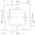
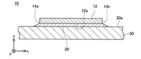
12 :半導体チップ
14a〜14d:辺
20 :はんだ層
30 :導体板
35a〜35d:傾斜面
Claims (1)
- 半導体装置であって、
導体板と、
前記導体板上に配置された半導体チップと、
前記導体板の上面と前記半導体チップの下面とを接続する接合材、
を有し、
前記半導体チップの前記下面の輪郭が、対辺の位置関係にある一対の辺を有し、
前記導体板の上面が、前記一対の辺の一方に接する第1傾斜面と、前記一対の辺の他方に接する第2傾斜面を有し、
前記第1傾斜面と前記第2傾斜面が、前記半導体チップの外周側から前記半導体チップの中心側に向かうにしたがって下側に変位するように傾斜している、
半導体装置。
Priority Applications (1)
| Application Number | Priority Date | Filing Date | Title |
|---|---|---|---|
| JP2018036885A JP2019153643A (ja) | 2018-03-01 | 2018-03-01 | 半導体装置 |
Applications Claiming Priority (1)
| Application Number | Priority Date | Filing Date | Title |
|---|---|---|---|
| JP2018036885A JP2019153643A (ja) | 2018-03-01 | 2018-03-01 | 半導体装置 |
Publications (1)
| Publication Number | Publication Date |
|---|---|
| JP2019153643A true JP2019153643A (ja) | 2019-09-12 |
Family
ID=67946936
Family Applications (1)
| Application Number | Title | Priority Date | Filing Date |
|---|---|---|---|
| JP2018036885A Pending JP2019153643A (ja) | 2018-03-01 | 2018-03-01 | 半導体装置 |
Country Status (1)
| Country | Link |
|---|---|
| JP (1) | JP2019153643A (ja) |
Cited By (1)
| Publication number | Priority date | Publication date | Assignee | Title |
|---|---|---|---|---|
| CN113937010A (zh) * | 2021-12-16 | 2022-01-14 | 绍兴中芯集成电路制造股份有限公司 | 半导体装置的制造方法 |
Citations (3)
| Publication number | Priority date | Publication date | Assignee | Title |
|---|---|---|---|---|
| JP2008205301A (ja) * | 2007-02-21 | 2008-09-04 | Toshiba Corp | 半導体装置 |
| US20090166826A1 (en) * | 2007-12-27 | 2009-07-02 | Janducayan Omar A | Lead frame die attach paddles with sloped walls and backside grooves suitable for leadless packages |
| JP2015079906A (ja) * | 2013-10-18 | 2015-04-23 | 三菱電機株式会社 | 半導体装置 |
-
2018
- 2018-03-01 JP JP2018036885A patent/JP2019153643A/ja active Pending
Patent Citations (3)
| Publication number | Priority date | Publication date | Assignee | Title |
|---|---|---|---|---|
| JP2008205301A (ja) * | 2007-02-21 | 2008-09-04 | Toshiba Corp | 半導体装置 |
| US20090166826A1 (en) * | 2007-12-27 | 2009-07-02 | Janducayan Omar A | Lead frame die attach paddles with sloped walls and backside grooves suitable for leadless packages |
| JP2015079906A (ja) * | 2013-10-18 | 2015-04-23 | 三菱電機株式会社 | 半導体装置 |
Cited By (1)
| Publication number | Priority date | Publication date | Assignee | Title |
|---|---|---|---|---|
| CN113937010A (zh) * | 2021-12-16 | 2022-01-14 | 绍兴中芯集成电路制造股份有限公司 | 半导体装置的制造方法 |
Similar Documents
| Publication | Publication Date | Title |
|---|---|---|
| EP3379572B1 (en) | Semiconductor device, manufacturing method for semiconductor device, and electrode plate | |
| JP6344919B2 (ja) | プリント回路板及び積層型半導体装置 | |
| JPS6076189A (ja) | 集積回路パツケージのアラインメントの方法 | |
| JP2019161174A (ja) | 半導体装置及び半導体装置の製造方法 | |
| JP5733401B2 (ja) | 半導体装置および半導体装置の製造方法 | |
| JP2019153643A (ja) | 半導体装置 | |
| JP6213946B2 (ja) | 回路基板の接合方法及び半導体モジュールの製造方法 | |
| JP2003124262A5 (ja) | ||
| TW201417645A (zh) | 焊接定位結構 | |
| JP2674501B2 (ja) | シングル・ポイント・ボンディング方法 | |
| JP2002158258A (ja) | 半導体装置、及び半導体装置の製造方法 | |
| JP5892184B2 (ja) | 半導体装置及び半導体装置の製造方法 | |
| JPH08203956A (ja) | 電子部品の製造方法及び電子部品 | |
| JP5889160B2 (ja) | 電子機器の製造方法 | |
| JP2021027146A (ja) | 半導体装置 | |
| CN114556534A (zh) | 半导体装置及半导体装置的制造方法 | |
| TWI518860B (zh) | 功率控制器件及其製備方法 | |
| JP2005072098A (ja) | 半導体装置 | |
| TW202109690A (zh) | 植球方法 | |
| JP6713334B2 (ja) | 基板構造 | |
| JPH071773B2 (ja) | 電子部品の接続構造 | |
| JP2004031693A (ja) | 半導体装置 | |
| JP2018078135A (ja) | 半導体装置 | |
| JPH0391990A (ja) | 半導体装置のボンディング方法及びボンディング装置 | |
| JP2023043017A (ja) | 半導体装置 |
Legal Events
| Date | Code | Title | Description |
|---|---|---|---|
| A711 | Notification of change in applicant |
Free format text: JAPANESE INTERMEDIATE CODE: A711 Effective date: 20200401 |
|
| A621 | Written request for application examination |
Free format text: JAPANESE INTERMEDIATE CODE: A621 Effective date: 20210219 |
|
| A977 | Report on retrieval |
Free format text: JAPANESE INTERMEDIATE CODE: A971007 Effective date: 20211122 |
|
| A131 | Notification of reasons for refusal |
Free format text: JAPANESE INTERMEDIATE CODE: A131 Effective date: 20211130 |
|
| A02 | Decision of refusal |
Free format text: JAPANESE INTERMEDIATE CODE: A02 Effective date: 20220524 |