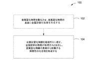
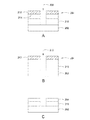
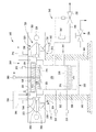
JP2018511935A - 金属窒化物を選択的に除去するためにアルキルアミンを使用する方法及び装置 - Google Patents
金属窒化物を選択的に除去するためにアルキルアミンを使用する方法及び装置 Download PDFInfo
- Publication number
- JP2018511935A JP2018511935A JP2017544596A JP2017544596A JP2018511935A JP 2018511935 A JP2018511935 A JP 2018511935A JP 2017544596 A JP2017544596 A JP 2017544596A JP 2017544596 A JP2017544596 A JP 2017544596A JP 2018511935 A JP2018511935 A JP 2018511935A
- Authority
- JP
- Japan
- Prior art keywords
- metal nitride
- nitride layer
- reactor
- layer
- metal
- Prior art date
- Legal status (The legal status is an assumption and is not a legal conclusion. Google has not performed a legal analysis and makes no representation as to the accuracy of the status listed.)
- Pending
Links
Images
Classifications
-
- H—ELECTRICITY
- H01—ELECTRIC ELEMENTS
- H01L—SEMICONDUCTOR DEVICES NOT COVERED BY CLASS H10
- H01L21/00—Processes or apparatus adapted for the manufacture or treatment of semiconductor or solid state devices or of parts thereof
- H01L21/02—Manufacture or treatment of semiconductor devices or of parts thereof
- H01L21/04—Manufacture or treatment of semiconductor devices or of parts thereof the devices having potential barriers, e.g. a PN junction, depletion layer or carrier concentration layer
- H01L21/18—Manufacture or treatment of semiconductor devices or of parts thereof the devices having potential barriers, e.g. a PN junction, depletion layer or carrier concentration layer the devices having semiconductor bodies comprising elements of Group IV of the Periodic Table or AIIIBV compounds with or without impurities, e.g. doping materials
- H01L21/30—Treatment of semiconductor bodies using processes or apparatus not provided for in groups H01L21/20 - H01L21/26
- H01L21/31—Treatment of semiconductor bodies using processes or apparatus not provided for in groups H01L21/20 - H01L21/26 to form insulating layers thereon, e.g. for masking or by using photolithographic techniques; After treatment of these layers; Selection of materials for these layers
- H01L21/3205—Deposition of non-insulating-, e.g. conductive- or resistive-, layers on insulating layers; After-treatment of these layers
- H01L21/321—After treatment
- H01L21/3213—Physical or chemical etching of the layers, e.g. to produce a patterned layer from a pre-deposited extensive layer
- H01L21/32133—Physical or chemical etching of the layers, e.g. to produce a patterned layer from a pre-deposited extensive layer by chemical means only
- H01L21/32135—Physical or chemical etching of the layers, e.g. to produce a patterned layer from a pre-deposited extensive layer by chemical means only by vapour etching only
-
- H—ELECTRICITY
- H01—ELECTRIC ELEMENTS
- H01L—SEMICONDUCTOR DEVICES NOT COVERED BY CLASS H10
- H01L21/00—Processes or apparatus adapted for the manufacture or treatment of semiconductor or solid state devices or of parts thereof
- H01L21/02—Manufacture or treatment of semiconductor devices or of parts thereof
- H01L21/02104—Forming layers
- H01L21/02107—Forming insulating materials on a substrate
- H01L21/02225—Forming insulating materials on a substrate characterised by the process for the formation of the insulating layer
- H01L21/02227—Forming insulating materials on a substrate characterised by the process for the formation of the insulating layer formation by a process other than a deposition process
- H01L21/0223—Forming insulating materials on a substrate characterised by the process for the formation of the insulating layer formation by a process other than a deposition process formation by oxidation, e.g. oxidation of the substrate
- H01L21/02244—Forming insulating materials on a substrate characterised by the process for the formation of the insulating layer formation by a process other than a deposition process formation by oxidation, e.g. oxidation of the substrate of a metallic layer
-
- H—ELECTRICITY
- H01—ELECTRIC ELEMENTS
- H01L—SEMICONDUCTOR DEVICES NOT COVERED BY CLASS H10
- H01L21/00—Processes or apparatus adapted for the manufacture or treatment of semiconductor or solid state devices or of parts thereof
- H01L21/02—Manufacture or treatment of semiconductor devices or of parts thereof
- H01L21/04—Manufacture or treatment of semiconductor devices or of parts thereof the devices having potential barriers, e.g. a PN junction, depletion layer or carrier concentration layer
- H01L21/18—Manufacture or treatment of semiconductor devices or of parts thereof the devices having potential barriers, e.g. a PN junction, depletion layer or carrier concentration layer the devices having semiconductor bodies comprising elements of Group IV of the Periodic Table or AIIIBV compounds with or without impurities, e.g. doping materials
- H01L21/30—Treatment of semiconductor bodies using processes or apparatus not provided for in groups H01L21/20 - H01L21/26
- H01L21/302—Treatment of semiconductor bodies using processes or apparatus not provided for in groups H01L21/20 - H01L21/26 to change their surface-physical characteristics or shape, e.g. etching, polishing, cutting
- H01L21/306—Chemical or electrical treatment, e.g. electrolytic etching
-
- H—ELECTRICITY
- H01—ELECTRIC ELEMENTS
- H01L—SEMICONDUCTOR DEVICES NOT COVERED BY CLASS H10
- H01L21/00—Processes or apparatus adapted for the manufacture or treatment of semiconductor or solid state devices or of parts thereof
- H01L21/02—Manufacture or treatment of semiconductor devices or of parts thereof
- H01L21/04—Manufacture or treatment of semiconductor devices or of parts thereof the devices having potential barriers, e.g. a PN junction, depletion layer or carrier concentration layer
- H01L21/18—Manufacture or treatment of semiconductor devices or of parts thereof the devices having potential barriers, e.g. a PN junction, depletion layer or carrier concentration layer the devices having semiconductor bodies comprising elements of Group IV of the Periodic Table or AIIIBV compounds with or without impurities, e.g. doping materials
- H01L21/30—Treatment of semiconductor bodies using processes or apparatus not provided for in groups H01L21/20 - H01L21/26
- H01L21/31—Treatment of semiconductor bodies using processes or apparatus not provided for in groups H01L21/20 - H01L21/26 to form insulating layers thereon, e.g. for masking or by using photolithographic techniques; After treatment of these layers; Selection of materials for these layers
- H01L21/3105—After-treatment
- H01L21/311—Etching the insulating layers by chemical or physical means
- H01L21/31144—Etching the insulating layers by chemical or physical means using masks
-
- H—ELECTRICITY
- H01—ELECTRIC ELEMENTS
- H01L—SEMICONDUCTOR DEVICES NOT COVERED BY CLASS H10
- H01L21/00—Processes or apparatus adapted for the manufacture or treatment of semiconductor or solid state devices or of parts thereof
- H01L21/67—Apparatus specially adapted for handling semiconductor or electric solid state devices during manufacture or treatment thereof; Apparatus specially adapted for handling wafers during manufacture or treatment of semiconductor or electric solid state devices or components ; Apparatus not specifically provided for elsewhere
- H01L21/67005—Apparatus not specifically provided for elsewhere
- H01L21/67011—Apparatus for manufacture or treatment
- H01L21/67098—Apparatus for thermal treatment
- H01L21/67109—Apparatus for thermal treatment mainly by convection
-
- H—ELECTRICITY
- H01—ELECTRIC ELEMENTS
- H01L—SEMICONDUCTOR DEVICES NOT COVERED BY CLASS H10
- H01L21/00—Processes or apparatus adapted for the manufacture or treatment of semiconductor or solid state devices or of parts thereof
- H01L21/67—Apparatus specially adapted for handling semiconductor or electric solid state devices during manufacture or treatment thereof; Apparatus specially adapted for handling wafers during manufacture or treatment of semiconductor or electric solid state devices or components ; Apparatus not specifically provided for elsewhere
- H01L21/67005—Apparatus not specifically provided for elsewhere
- H01L21/67011—Apparatus for manufacture or treatment
- H01L21/67155—Apparatus for manufacturing or treating in a plurality of work-stations
- H01L21/6719—Apparatus for manufacturing or treating in a plurality of work-stations characterized by the construction of the processing chambers, e.g. modular processing chambers
-
- H—ELECTRICITY
- H01—ELECTRIC ELEMENTS
- H01L—SEMICONDUCTOR DEVICES NOT COVERED BY CLASS H10
- H01L21/00—Processes or apparatus adapted for the manufacture or treatment of semiconductor or solid state devices or of parts thereof
- H01L21/67—Apparatus specially adapted for handling semiconductor or electric solid state devices during manufacture or treatment thereof; Apparatus specially adapted for handling wafers during manufacture or treatment of semiconductor or electric solid state devices or components ; Apparatus not specifically provided for elsewhere
- H01L21/683—Apparatus specially adapted for handling semiconductor or electric solid state devices during manufacture or treatment thereof; Apparatus specially adapted for handling wafers during manufacture or treatment of semiconductor or electric solid state devices or components ; Apparatus not specifically provided for elsewhere for supporting or gripping
- H01L21/6838—Apparatus specially adapted for handling semiconductor or electric solid state devices during manufacture or treatment thereof; Apparatus specially adapted for handling wafers during manufacture or treatment of semiconductor or electric solid state devices or components ; Apparatus not specifically provided for elsewhere for supporting or gripping with gripping and holding devices using a vacuum; Bernoulli devices
-
- H—ELECTRICITY
- H01—ELECTRIC ELEMENTS
- H01L—SEMICONDUCTOR DEVICES NOT COVERED BY CLASS H10
- H01L21/00—Processes or apparatus adapted for the manufacture or treatment of semiconductor or solid state devices or of parts thereof
- H01L21/02—Manufacture or treatment of semiconductor devices or of parts thereof
- H01L21/04—Manufacture or treatment of semiconductor devices or of parts thereof the devices having potential barriers, e.g. a PN junction, depletion layer or carrier concentration layer
- H01L21/18—Manufacture or treatment of semiconductor devices or of parts thereof the devices having potential barriers, e.g. a PN junction, depletion layer or carrier concentration layer the devices having semiconductor bodies comprising elements of Group IV of the Periodic Table or AIIIBV compounds with or without impurities, e.g. doping materials
- H01L21/30—Treatment of semiconductor bodies using processes or apparatus not provided for in groups H01L21/20 - H01L21/26
- H01L21/31—Treatment of semiconductor bodies using processes or apparatus not provided for in groups H01L21/20 - H01L21/26 to form insulating layers thereon, e.g. for masking or by using photolithographic techniques; After treatment of these layers; Selection of materials for these layers
- H01L21/3205—Deposition of non-insulating-, e.g. conductive- or resistive-, layers on insulating layers; After-treatment of these layers
- H01L21/321—After treatment
- H01L21/3213—Physical or chemical etching of the layers, e.g. to produce a patterned layer from a pre-deposited extensive layer
- H01L21/32139—Physical or chemical etching of the layers, e.g. to produce a patterned layer from a pre-deposited extensive layer using masks
Landscapes
- Engineering & Computer Science (AREA)
- General Physics & Mathematics (AREA)
- Physics & Mathematics (AREA)
- Condensed Matter Physics & Semiconductors (AREA)
- Manufacturing & Machinery (AREA)
- Computer Hardware Design (AREA)
- Microelectronics & Electronic Packaging (AREA)
- Power Engineering (AREA)
- General Chemical & Material Sciences (AREA)
- Chemical Kinetics & Catalysis (AREA)
- Chemical & Material Sciences (AREA)
- Internal Circuitry In Semiconductor Integrated Circuit Devices (AREA)
- Drying Of Semiconductors (AREA)
- Weting (AREA)
Applications Claiming Priority (3)
| Application Number | Priority Date | Filing Date | Title |
|---|---|---|---|
| IN551DE2015 | 2015-02-25 | ||
| IN551/DEL/2015 | 2015-02-25 | ||
| PCT/US2016/019484 WO2016138218A1 (en) | 2015-02-25 | 2016-02-25 | Methods and apparatus for using alkyl amines for the selective removal of metal nitride |
Publications (2)
| Publication Number | Publication Date |
|---|---|
| JP2018511935A true JP2018511935A (ja) | 2018-04-26 |
| JP2018511935A5 JP2018511935A5 (enExample) | 2019-04-11 |
Family
ID=56789186
Family Applications (1)
| Application Number | Title | Priority Date | Filing Date |
|---|---|---|---|
| JP2017544596A Pending JP2018511935A (ja) | 2015-02-25 | 2016-02-25 | 金属窒化物を選択的に除去するためにアルキルアミンを使用する方法及び装置 |
Country Status (6)
| Country | Link |
|---|---|
| US (1) | US20180033643A1 (enExample) |
| JP (1) | JP2018511935A (enExample) |
| KR (1) | KR20170121243A (enExample) |
| CN (1) | CN107258010A (enExample) |
| TW (1) | TW201703130A (enExample) |
| WO (1) | WO2016138218A1 (enExample) |
Cited By (1)
| Publication number | Priority date | Publication date | Assignee | Title |
|---|---|---|---|---|
| JP2024527376A (ja) * | 2021-07-12 | 2024-07-24 | アプライド マテリアルズ インコーポレイテッド | 遷移金属窒化物材料の選択的除去 |
Families Citing this family (24)
| Publication number | Priority date | Publication date | Assignee | Title |
|---|---|---|---|---|
| US9132436B2 (en) | 2012-09-21 | 2015-09-15 | Applied Materials, Inc. | Chemical control features in wafer process equipment |
| US10256079B2 (en) | 2013-02-08 | 2019-04-09 | Applied Materials, Inc. | Semiconductor processing systems having multiple plasma configurations |
| US11637002B2 (en) | 2014-11-26 | 2023-04-25 | Applied Materials, Inc. | Methods and systems to enhance process uniformity |
| US20160225652A1 (en) | 2015-02-03 | 2016-08-04 | Applied Materials, Inc. | Low temperature chuck for plasma processing systems |
| US9741593B2 (en) | 2015-08-06 | 2017-08-22 | Applied Materials, Inc. | Thermal management systems and methods for wafer processing systems |
| US10504700B2 (en) | 2015-08-27 | 2019-12-10 | Applied Materials, Inc. | Plasma etching systems and methods with secondary plasma injection |
| US10504754B2 (en) | 2016-05-19 | 2019-12-10 | Applied Materials, Inc. | Systems and methods for improved semiconductor etching and component protection |
| US9865484B1 (en) | 2016-06-29 | 2018-01-09 | Applied Materials, Inc. | Selective etch using material modification and RF pulsing |
| US10546729B2 (en) | 2016-10-04 | 2020-01-28 | Applied Materials, Inc. | Dual-channel showerhead with improved profile |
| US10043684B1 (en) * | 2017-02-06 | 2018-08-07 | Applied Materials, Inc. | Self-limiting atomic thermal etching systems and methods |
| US10014185B1 (en) * | 2017-03-01 | 2018-07-03 | Applied Materials, Inc. | Selective etch of metal nitride films |
| US11276590B2 (en) | 2017-05-17 | 2022-03-15 | Applied Materials, Inc. | Multi-zone semiconductor substrate supports |
| JP7176860B6 (ja) | 2017-05-17 | 2022-12-16 | アプライド マテリアルズ インコーポレイテッド | 前駆体の流れを改善する半導体処理チャンバ |
| US11276559B2 (en) | 2017-05-17 | 2022-03-15 | Applied Materials, Inc. | Semiconductor processing chamber for multiple precursor flow |
| US10297458B2 (en) | 2017-08-07 | 2019-05-21 | Applied Materials, Inc. | Process window widening using coated parts in plasma etch processes |
| US11328909B2 (en) | 2017-12-22 | 2022-05-10 | Applied Materials, Inc. | Chamber conditioning and removal processes |
| US10964512B2 (en) | 2018-02-15 | 2021-03-30 | Applied Materials, Inc. | Semiconductor processing chamber multistage mixing apparatus and methods |
| US10319600B1 (en) | 2018-03-12 | 2019-06-11 | Applied Materials, Inc. | Thermal silicon etch |
| US11049755B2 (en) | 2018-09-14 | 2021-06-29 | Applied Materials, Inc. | Semiconductor substrate supports with embedded RF shield |
| US11062887B2 (en) | 2018-09-17 | 2021-07-13 | Applied Materials, Inc. | High temperature RF heater pedestals |
| US11417534B2 (en) | 2018-09-21 | 2022-08-16 | Applied Materials, Inc. | Selective material removal |
| US11682560B2 (en) | 2018-10-11 | 2023-06-20 | Applied Materials, Inc. | Systems and methods for hafnium-containing film removal |
| US11121002B2 (en) | 2018-10-24 | 2021-09-14 | Applied Materials, Inc. | Systems and methods for etching metals and metal derivatives |
| US11437242B2 (en) | 2018-11-27 | 2022-09-06 | Applied Materials, Inc. | Selective removal of silicon-containing materials |
Citations (5)
| Publication number | Priority date | Publication date | Assignee | Title |
|---|---|---|---|---|
| JPH06140372A (ja) * | 1992-10-27 | 1994-05-20 | Nec Corp | 半導体装置の製造方法 |
| JPH11163138A (ja) * | 1997-11-28 | 1999-06-18 | Sony Corp | 半導体装置の製造方法 |
| JP2010045171A (ja) * | 2008-08-12 | 2010-02-25 | Hitachi High-Technologies Corp | 半導体加工方法 |
| JP2012114402A (ja) * | 2010-07-12 | 2012-06-14 | Central Glass Co Ltd | ドライエッチング剤 |
| JP2015529014A (ja) * | 2012-07-16 | 2015-10-01 | マットソン テクノロジー インコーポレイテッドMattson Technology, Inc. | 純還元性プラズマ中で高アスペクト比のフォトレジストを除去する方法 |
Family Cites Families (21)
| Publication number | Priority date | Publication date | Assignee | Title |
|---|---|---|---|---|
| JPH05283362A (ja) * | 1992-04-03 | 1993-10-29 | Sony Corp | 多層配線の形成方法 |
| US6849471B2 (en) * | 2003-03-28 | 2005-02-01 | Reflectivity, Inc. | Barrier layers for microelectromechanical systems |
| US6358788B1 (en) * | 1999-08-30 | 2002-03-19 | Micron Technology, Inc. | Method of fabricating a wordline in a memory array of a semiconductor device |
| JP4686006B2 (ja) * | 2000-04-27 | 2011-05-18 | 大日本印刷株式会社 | ハーフトーン位相シフトフォトマスクとハーフトーン位相シフトフォトマスク用ブランクス、及びハーフトーン位相シフトフォトマスクの製造方法 |
| JP2005067164A (ja) * | 2003-08-28 | 2005-03-17 | Sony Corp | 液体吐出ヘッド、液体吐出装置及び液体吐出ヘッドの製造方法 |
| US20060016783A1 (en) * | 2004-07-22 | 2006-01-26 | Dingjun Wu | Process for titanium nitride removal |
| JP3889023B2 (ja) * | 2005-08-05 | 2007-03-07 | シャープ株式会社 | 可変抵抗素子とその製造方法並びにそれを備えた記憶装置 |
| US20070117396A1 (en) * | 2005-11-22 | 2007-05-24 | Dingjun Wu | Selective etching of titanium nitride with xenon difluoride |
| JP5334199B2 (ja) * | 2008-01-22 | 2013-11-06 | ルネサスエレクトロニクス株式会社 | 容量素子を有する半導体装置 |
| JP5590113B2 (ja) * | 2010-03-02 | 2014-09-17 | 旭硝子株式会社 | Euvリソグラフィ用反射型マスクブランクおよびその製造方法 |
| US9831088B2 (en) * | 2010-10-06 | 2017-11-28 | Entegris, Inc. | Composition and process for selectively etching metal nitrides |
| WO2013101907A1 (en) * | 2011-12-28 | 2013-07-04 | Advanced Technology Materials, Inc. | Compositions and methods for selectively etching titanium nitride |
| US8987133B2 (en) * | 2013-01-15 | 2015-03-24 | International Business Machines Corporation | Titanium oxynitride hard mask for lithographic patterning |
| JP2014154866A (ja) * | 2013-02-14 | 2014-08-25 | Fujifilm Corp | ドライエッチング装置及びドライエッチング装置用のクランプ |
| JP6336866B2 (ja) * | 2013-10-23 | 2018-06-06 | 株式会社日立国際電気 | 半導体デバイスの製造方法、基板処理装置およびプログラム |
| US9543157B2 (en) * | 2014-09-30 | 2017-01-10 | Infineon Technologies Ag | Method for processing a carrier, a method for operating a plasma processing chamber, and a method for processing a semiconductor wafer |
| JP6523091B2 (ja) * | 2015-07-24 | 2019-05-29 | 株式会社Kokusai Electric | 半導体装置の製造方法、基板処理装置およびプログラム |
| JP6462602B2 (ja) * | 2016-01-12 | 2019-01-30 | 信越化学工業株式会社 | 多層膜形成方法及びパターン形成方法 |
| US10522467B2 (en) * | 2016-07-06 | 2019-12-31 | Tokyo Electron Limited | Ruthenium wiring and manufacturing method thereof |
| US9941142B1 (en) * | 2017-01-12 | 2018-04-10 | International Business Machines Corporation | Tunable TiOxNy hardmask for multilayer patterning |
| US10014185B1 (en) * | 2017-03-01 | 2018-07-03 | Applied Materials, Inc. | Selective etch of metal nitride films |
-
2016
- 2016-02-25 KR KR1020177026904A patent/KR20170121243A/ko not_active Withdrawn
- 2016-02-25 WO PCT/US2016/019484 patent/WO2016138218A1/en not_active Ceased
- 2016-02-25 JP JP2017544596A patent/JP2018511935A/ja active Pending
- 2016-02-25 TW TW105105685A patent/TW201703130A/zh unknown
- 2016-02-25 CN CN201680010536.9A patent/CN107258010A/zh active Pending
- 2016-02-25 US US15/552,207 patent/US20180033643A1/en not_active Abandoned
Patent Citations (5)
| Publication number | Priority date | Publication date | Assignee | Title |
|---|---|---|---|---|
| JPH06140372A (ja) * | 1992-10-27 | 1994-05-20 | Nec Corp | 半導体装置の製造方法 |
| JPH11163138A (ja) * | 1997-11-28 | 1999-06-18 | Sony Corp | 半導体装置の製造方法 |
| JP2010045171A (ja) * | 2008-08-12 | 2010-02-25 | Hitachi High-Technologies Corp | 半導体加工方法 |
| JP2012114402A (ja) * | 2010-07-12 | 2012-06-14 | Central Glass Co Ltd | ドライエッチング剤 |
| JP2015529014A (ja) * | 2012-07-16 | 2015-10-01 | マットソン テクノロジー インコーポレイテッドMattson Technology, Inc. | 純還元性プラズマ中で高アスペクト比のフォトレジストを除去する方法 |
Cited By (2)
| Publication number | Priority date | Publication date | Assignee | Title |
|---|---|---|---|---|
| JP2024527376A (ja) * | 2021-07-12 | 2024-07-24 | アプライド マテリアルズ インコーポレイテッド | 遷移金属窒化物材料の選択的除去 |
| JP7678213B2 (ja) | 2021-07-12 | 2025-05-15 | アプライド マテリアルズ インコーポレイテッド | 遷移金属窒化物材料の選択的除去 |
Also Published As
| Publication number | Publication date |
|---|---|
| TW201703130A (zh) | 2017-01-16 |
| WO2016138218A8 (en) | 2017-03-16 |
| US20180033643A1 (en) | 2018-02-01 |
| WO2016138218A1 (en) | 2016-09-01 |
| KR20170121243A (ko) | 2017-11-01 |
| CN107258010A (zh) | 2017-10-17 |
Similar Documents
| Publication | Publication Date | Title |
|---|---|---|
| JP2018511935A (ja) | 金属窒化物を選択的に除去するためにアルキルアミンを使用する方法及び装置 | |
| KR102360672B1 (ko) | 무수 식각 방법들 | |
| JP7184810B2 (ja) | 基板に堆積された膜の品質改善 | |
| KR102206927B1 (ko) | 금속을 함유하는 화합물들을 에칭하기 위한 다단계 방법 및 장치 | |
| JP2018511935A5 (enExample) | ||
| US9997373B2 (en) | Technique to deposit sidewall passivation for high aspect ratio cylinder etch | |
| US10373840B2 (en) | Technique to deposit sidewall passivation for high aspect ratio cylinder etch | |
| US9887097B2 (en) | Technique to deposit sidewall passivation for high aspect ratio cylinder etch | |
| CN104685610B (zh) | 使用低温蚀刻剂沉积与等离子体后处理的方向性二氧化硅蚀刻 | |
| JP7161520B2 (ja) | シリコンベース誘電体への選択的堆積のための方法 | |
| US20190311896A1 (en) | Method to fabricate thermally stable low k-finfet spacer | |
| US8951913B2 (en) | Method for removing native oxide and associated residue from a substrate | |
| JP6469705B2 (ja) | エッチング後のインターフェースを安定化し、次の処理ステップ前のキュータイム問題を最小化する方法 | |
| KR20170013832A (ko) | 센서티브 재료들 상에 할라이드 함유 ald 막을 집적하는 방법 | |
| CN105900214A (zh) | 通过使用远程等离子体pecvd的fcvd硬件形成的可流动碳膜 | |
| WO2018222771A1 (en) | Dry stripping of boron carbide hardmask | |
| CN112602169A (zh) | 在含硅表面上的选择性沉积 | |
| WO2018026867A1 (en) | Technique to deposit sidewall passivation for high aspect ratio cylinder etch | |
| JP4999419B2 (ja) | 基板処理方法および基板処理システム、ならびにコンピュータ読取可能な記憶媒体 | |
| US20170125241A1 (en) | Low temp single precursor arc hard mask for multilayer patterning application | |
| US20250188600A1 (en) | Sidewall passivation using aldehyde or isocyanate chemistry for high aspect ratio etch | |
| US10818490B2 (en) | Controlled growth of thin silicon oxide film at low temperature | |
| TWI869676B (zh) | 金屬氧化物滲入光阻劑中之方法及半導體處理系統 | |
| JP7580386B2 (ja) | 熱酸化品質が高い厚い酸化膜を低温で成長させる方法 | |
| US20240234162A9 (en) | Substrate-processing method and substrate-processing apparatus |
Legal Events
| Date | Code | Title | Description |
|---|---|---|---|
| A521 | Request for written amendment filed |
Free format text: JAPANESE INTERMEDIATE CODE: A523 Effective date: 20190225 |
|
| A621 | Written request for application examination |
Free format text: JAPANESE INTERMEDIATE CODE: A621 Effective date: 20190225 |
|
| A977 | Report on retrieval |
Free format text: JAPANESE INTERMEDIATE CODE: A971007 Effective date: 20200422 |
|
| A131 | Notification of reasons for refusal |
Free format text: JAPANESE INTERMEDIATE CODE: A131 Effective date: 20200519 |
|
| A02 | Decision of refusal |
Free format text: JAPANESE INTERMEDIATE CODE: A02 Effective date: 20201222 |