JP2018107725A - 光電変換装置、撮像システム - Google Patents
光電変換装置、撮像システム Download PDFInfo
- Publication number
- JP2018107725A JP2018107725A JP2016254364A JP2016254364A JP2018107725A JP 2018107725 A JP2018107725 A JP 2018107725A JP 2016254364 A JP2016254364 A JP 2016254364A JP 2016254364 A JP2016254364 A JP 2016254364A JP 2018107725 A JP2018107725 A JP 2018107725A
- Authority
- JP
- Japan
- Prior art keywords
- photoelectric conversion
- voltage
- electrode
- signal
- node
- Prior art date
- Legal status (The legal status is an assumption and is not a legal conclusion. Google has not performed a legal analysis and makes no representation as to the accuracy of the status listed.)
- Pending
Links
- 238000006243 chemical reaction Methods 0.000 title claims abstract description 352
- 238000003384 imaging method Methods 0.000 title claims description 58
- 230000000903 blocking effect Effects 0.000 claims description 75
- 239000004065 semiconductor Substances 0.000 claims description 74
- 230000003321 amplification Effects 0.000 claims description 55
- 238000003199 nucleic acid amplification method Methods 0.000 claims description 55
- 239000000758 substrate Substances 0.000 claims description 35
- 239000012535 impurity Substances 0.000 claims description 34
- 238000009792 diffusion process Methods 0.000 claims description 29
- 238000012545 processing Methods 0.000 claims description 17
- 238000009825 accumulation Methods 0.000 claims description 16
- 238000002347 injection Methods 0.000 claims description 12
- 239000007924 injection Substances 0.000 claims description 12
- 239000010410 layer Substances 0.000 description 193
- 239000003990 capacitor Substances 0.000 description 46
- 239000000463 material Substances 0.000 description 33
- 238000010586 diagram Methods 0.000 description 28
- 230000003287 optical effect Effects 0.000 description 26
- 230000008859 change Effects 0.000 description 16
- 230000007423 decrease Effects 0.000 description 9
- 230000000694 effects Effects 0.000 description 8
- 230000006870 function Effects 0.000 description 8
- 150000001875 compounds Chemical class 0.000 description 5
- 229910021417 amorphous silicon Inorganic materials 0.000 description 4
- 239000010408 film Substances 0.000 description 4
- 229910052751 metal Inorganic materials 0.000 description 4
- 239000002184 metal Substances 0.000 description 4
- 238000000034 method Methods 0.000 description 4
- 230000008569 process Effects 0.000 description 4
- 238000005096 rolling process Methods 0.000 description 4
- 230000035945 sensitivity Effects 0.000 description 4
- XUIMIQQOPSSXEZ-UHFFFAOYSA-N Silicon Chemical compound [Si] XUIMIQQOPSSXEZ-UHFFFAOYSA-N 0.000 description 3
- 238000004364 calculation method Methods 0.000 description 3
- 239000011159 matrix material Substances 0.000 description 3
- 239000002096 quantum dot Substances 0.000 description 3
- 230000009467 reduction Effects 0.000 description 3
- 230000000630 rising effect Effects 0.000 description 3
- 229910052710 silicon Inorganic materials 0.000 description 3
- 239000010703 silicon Substances 0.000 description 3
- 238000012546 transfer Methods 0.000 description 3
- JBRZTFJDHDCESZ-UHFFFAOYSA-N AsGa Chemical compound [As]#[Ga] JBRZTFJDHDCESZ-UHFFFAOYSA-N 0.000 description 2
- 229910001218 Gallium arsenide Inorganic materials 0.000 description 2
- 230000004888 barrier function Effects 0.000 description 2
- VYXSBFYARXAAKO-WTKGSRSZSA-N chembl402140 Chemical compound Cl.C1=2C=C(C)C(NCC)=CC=2OC2=C\C(=N/CC)C(C)=CC2=C1C1=CC=CC=C1C(=O)OCC VYXSBFYARXAAKO-WTKGSRSZSA-N 0.000 description 2
- 230000003247 decreasing effect Effects 0.000 description 2
- 230000007547 defect Effects 0.000 description 2
- 238000007599 discharging Methods 0.000 description 2
- 238000004519 manufacturing process Methods 0.000 description 2
- 239000002245 particle Substances 0.000 description 2
- IEQIEDJGQAUEQZ-UHFFFAOYSA-N phthalocyanine Chemical compound N1C(N=C2C3=CC=CC=C3C(N=C3C4=CC=CC=C4C(=N4)N3)=N2)=C(C=CC=C2)C2=C1N=C1C2=CC=CC=C2C4=N1 IEQIEDJGQAUEQZ-UHFFFAOYSA-N 0.000 description 2
- 229910017115 AlSb Inorganic materials 0.000 description 1
- XMWRBQBLMFGWIX-UHFFFAOYSA-N C60 fullerene Chemical compound C12=C3C(C4=C56)=C7C8=C5C5=C9C%10=C6C6=C4C1=C1C4=C6C6=C%10C%10=C9C9=C%11C5=C8C5=C8C7=C3C3=C7C2=C1C1=C2C4=C6C4=C%10C6=C9C9=C%11C5=C5C8=C3C3=C7C1=C1C2=C4C6=C2C9=C5C3=C12 XMWRBQBLMFGWIX-UHFFFAOYSA-N 0.000 description 1
- 229910005540 GaP Inorganic materials 0.000 description 1
- NRCMAYZCPIVABH-UHFFFAOYSA-N Quinacridone Chemical compound N1C2=CC=CC=C2C(=O)C2=C1C=C1C(=O)C3=CC=CC=C3NC1=C2 NRCMAYZCPIVABH-UHFFFAOYSA-N 0.000 description 1
- 229910010421 TiNx Inorganic materials 0.000 description 1
- ATJFFYVFTNAWJD-UHFFFAOYSA-N Tin Chemical compound [Sn] ATJFFYVFTNAWJD-UHFFFAOYSA-N 0.000 description 1
- HCHKCACWOHOZIP-UHFFFAOYSA-N Zinc Chemical compound [Zn] HCHKCACWOHOZIP-UHFFFAOYSA-N 0.000 description 1
- 230000005540 biological transmission Effects 0.000 description 1
- UHYPYGJEEGLRJD-UHFFFAOYSA-N cadmium(2+);selenium(2-) Chemical compound [Se-2].[Cd+2] UHYPYGJEEGLRJD-UHFFFAOYSA-N 0.000 description 1
- 239000000969 carrier Substances 0.000 description 1
- 238000007906 compression Methods 0.000 description 1
- 230000006835 compression Effects 0.000 description 1
- 238000012937 correction Methods 0.000 description 1
- VBVAVBCYMYWNOU-UHFFFAOYSA-N coumarin 6 Chemical compound C1=CC=C2SC(C3=CC4=CC=C(C=C4OC3=O)N(CC)CC)=NC2=C1 VBVAVBCYMYWNOU-UHFFFAOYSA-N 0.000 description 1
- 230000008034 disappearance Effects 0.000 description 1
- 239000003574 free electron Substances 0.000 description 1
- 229910003472 fullerene Inorganic materials 0.000 description 1
- 229910052732 germanium Inorganic materials 0.000 description 1
- GNPVGFCGXDBREM-UHFFFAOYSA-N germanium atom Chemical compound [Ge] GNPVGFCGXDBREM-UHFFFAOYSA-N 0.000 description 1
- 229910052738 indium Inorganic materials 0.000 description 1
- APFVFJFRJDLVQX-UHFFFAOYSA-N indium atom Chemical compound [In] APFVFJFRJDLVQX-UHFFFAOYSA-N 0.000 description 1
- 239000011229 interlayer Substances 0.000 description 1
- 239000000203 mixture Substances 0.000 description 1
- 238000012986 modification Methods 0.000 description 1
- 230000004048 modification Effects 0.000 description 1
- LKKPNUDVOYAOBB-UHFFFAOYSA-N naphthalocyanine Chemical compound N1C(N=C2C3=CC4=CC=CC=C4C=C3C(N=C3C4=CC5=CC=CC=C5C=C4C(=N4)N3)=N2)=C(C=C2C(C=CC=C2)=C2)C2=C1N=C1C2=CC3=CC=CC=C3C=C2C4=N1 LKKPNUDVOYAOBB-UHFFFAOYSA-N 0.000 description 1
- 230000003071 parasitic effect Effects 0.000 description 1
- 229910021420 polycrystalline silicon Inorganic materials 0.000 description 1
- 229920005591 polysilicon Polymers 0.000 description 1
- 238000005036 potential barrier Methods 0.000 description 1
- 230000006798 recombination Effects 0.000 description 1
- 238000005215 recombination Methods 0.000 description 1
- 230000004044 response Effects 0.000 description 1
- 238000003860 storage Methods 0.000 description 1
- 239000010409 thin film Substances 0.000 description 1
- 229910052725 zinc Inorganic materials 0.000 description 1
- 239000011701 zinc Substances 0.000 description 1
Images


Classifications
-
- H—ELECTRICITY
- H04—ELECTRIC COMMUNICATION TECHNIQUE
- H04N—PICTORIAL COMMUNICATION, e.g. TELEVISION
- H04N25/00—Circuitry of solid-state image sensors [SSIS]; Control thereof
- H04N25/40—Extracting pixel data from image sensors by controlling scanning circuits, e.g. by modifying the number of pixels sampled or to be sampled
- H04N25/44—Extracting pixel data from image sensors by controlling scanning circuits, e.g. by modifying the number of pixels sampled or to be sampled by partially reading an SSIS array
-
- G—PHYSICS
- G01—MEASURING; TESTING
- G01C—MEASURING DISTANCES, LEVELS OR BEARINGS; SURVEYING; NAVIGATION; GYROSCOPIC INSTRUMENTS; PHOTOGRAMMETRY OR VIDEOGRAMMETRY
- G01C3/00—Measuring distances in line of sight; Optical rangefinders
- G01C3/02—Details
- G01C3/06—Use of electric means to obtain final indication
- G01C3/08—Use of electric radiation detectors
- G01C3/085—Use of electric radiation detectors with electronic parallax measurement
-
- H—ELECTRICITY
- H01—ELECTRIC ELEMENTS
- H01L—SEMICONDUCTOR DEVICES NOT COVERED BY CLASS H10
- H01L27/00—Devices consisting of a plurality of semiconductor or other solid-state components formed in or on a common substrate
- H01L27/14—Devices consisting of a plurality of semiconductor or other solid-state components formed in or on a common substrate including semiconductor components sensitive to infrared radiation, light, electromagnetic radiation of shorter wavelength or corpuscular radiation and specially adapted either for the conversion of the energy of such radiation into electrical energy or for the control of electrical energy by such radiation
- H01L27/144—Devices controlled by radiation
- H01L27/146—Imager structures
- H01L27/14601—Structural or functional details thereof
- H01L27/14609—Pixel-elements with integrated switching, control, storage or amplification elements
- H01L27/1461—Pixel-elements with integrated switching, control, storage or amplification elements characterised by the photosensitive area
-
- H—ELECTRICITY
- H01—ELECTRIC ELEMENTS
- H01L—SEMICONDUCTOR DEVICES NOT COVERED BY CLASS H10
- H01L27/00—Devices consisting of a plurality of semiconductor or other solid-state components formed in or on a common substrate
- H01L27/14—Devices consisting of a plurality of semiconductor or other solid-state components formed in or on a common substrate including semiconductor components sensitive to infrared radiation, light, electromagnetic radiation of shorter wavelength or corpuscular radiation and specially adapted either for the conversion of the energy of such radiation into electrical energy or for the control of electrical energy by such radiation
- H01L27/144—Devices controlled by radiation
- H01L27/146—Imager structures
- H01L27/14601—Structural or functional details thereof
- H01L27/14609—Pixel-elements with integrated switching, control, storage or amplification elements
- H01L27/14612—Pixel-elements with integrated switching, control, storage or amplification elements involving a transistor
-
- H—ELECTRICITY
- H01—ELECTRIC ELEMENTS
- H01L—SEMICONDUCTOR DEVICES NOT COVERED BY CLASS H10
- H01L27/00—Devices consisting of a plurality of semiconductor or other solid-state components formed in or on a common substrate
- H01L27/14—Devices consisting of a plurality of semiconductor or other solid-state components formed in or on a common substrate including semiconductor components sensitive to infrared radiation, light, electromagnetic radiation of shorter wavelength or corpuscular radiation and specially adapted either for the conversion of the energy of such radiation into electrical energy or for the control of electrical energy by such radiation
- H01L27/144—Devices controlled by radiation
- H01L27/146—Imager structures
- H01L27/14601—Structural or functional details thereof
- H01L27/14625—Optical elements or arrangements associated with the device
- H01L27/14627—Microlenses
-
- H—ELECTRICITY
- H01—ELECTRIC ELEMENTS
- H01L—SEMICONDUCTOR DEVICES NOT COVERED BY CLASS H10
- H01L27/00—Devices consisting of a plurality of semiconductor or other solid-state components formed in or on a common substrate
- H01L27/14—Devices consisting of a plurality of semiconductor or other solid-state components formed in or on a common substrate including semiconductor components sensitive to infrared radiation, light, electromagnetic radiation of shorter wavelength or corpuscular radiation and specially adapted either for the conversion of the energy of such radiation into electrical energy or for the control of electrical energy by such radiation
- H01L27/144—Devices controlled by radiation
- H01L27/146—Imager structures
- H01L27/14601—Structural or functional details thereof
- H01L27/14636—Interconnect structures
-
- H—ELECTRICITY
- H01—ELECTRIC ELEMENTS
- H01L—SEMICONDUCTOR DEVICES NOT COVERED BY CLASS H10
- H01L27/00—Devices consisting of a plurality of semiconductor or other solid-state components formed in or on a common substrate
- H01L27/14—Devices consisting of a plurality of semiconductor or other solid-state components formed in or on a common substrate including semiconductor components sensitive to infrared radiation, light, electromagnetic radiation of shorter wavelength or corpuscular radiation and specially adapted either for the conversion of the energy of such radiation into electrical energy or for the control of electrical energy by such radiation
- H01L27/144—Devices controlled by radiation
- H01L27/146—Imager structures
- H01L27/14643—Photodiode arrays; MOS imagers
-
- H—ELECTRICITY
- H04—ELECTRIC COMMUNICATION TECHNIQUE
- H04N—PICTORIAL COMMUNICATION, e.g. TELEVISION
- H04N25/00—Circuitry of solid-state image sensors [SSIS]; Control thereof
- H04N25/50—Control of the SSIS exposure
- H04N25/53—Control of the integration time
-
- H—ELECTRICITY
- H04—ELECTRIC COMMUNICATION TECHNIQUE
- H04N—PICTORIAL COMMUNICATION, e.g. TELEVISION
- H04N25/00—Circuitry of solid-state image sensors [SSIS]; Control thereof
- H04N25/70—SSIS architectures; Circuits associated therewith
- H04N25/71—Charge-coupled device [CCD] sensors; Charge-transfer registers specially adapted for CCD sensors
- H04N25/75—Circuitry for providing, modifying or processing image signals from the pixel array
-
- H—ELECTRICITY
- H04—ELECTRIC COMMUNICATION TECHNIQUE
- H04N—PICTORIAL COMMUNICATION, e.g. TELEVISION
- H04N25/00—Circuitry of solid-state image sensors [SSIS]; Control thereof
- H04N25/70—SSIS architectures; Circuits associated therewith
- H04N25/76—Addressed sensors, e.g. MOS or CMOS sensors
-
- H—ELECTRICITY
- H04—ELECTRIC COMMUNICATION TECHNIQUE
- H04N—PICTORIAL COMMUNICATION, e.g. TELEVISION
- H04N25/00—Circuitry of solid-state image sensors [SSIS]; Control thereof
- H04N25/70—SSIS architectures; Circuits associated therewith
- H04N25/76—Addressed sensors, e.g. MOS or CMOS sensors
- H04N25/77—Pixel circuitry, e.g. memories, A/D converters, pixel amplifiers, shared circuits or shared components
- H04N25/778—Pixel circuitry, e.g. memories, A/D converters, pixel amplifiers, shared circuits or shared components comprising amplifiers shared between a plurality of pixels, i.e. at least one part of the amplifier must be on the sensor array itself
-
- B—PERFORMING OPERATIONS; TRANSPORTING
- B60—VEHICLES IN GENERAL
- B60W—CONJOINT CONTROL OF VEHICLE SUB-UNITS OF DIFFERENT TYPE OR DIFFERENT FUNCTION; CONTROL SYSTEMS SPECIALLY ADAPTED FOR HYBRID VEHICLES; ROAD VEHICLE DRIVE CONTROL SYSTEMS FOR PURPOSES NOT RELATED TO THE CONTROL OF A PARTICULAR SUB-UNIT
- B60W2420/00—Indexing codes relating to the type of sensors based on the principle of their operation
- B60W2420/40—Photo or light sensitive means, e.g. infrared sensors
- B60W2420/403—Image sensing, e.g. optical camera
-
- B—PERFORMING OPERATIONS; TRANSPORTING
- B60—VEHICLES IN GENERAL
- B60W—CONJOINT CONTROL OF VEHICLE SUB-UNITS OF DIFFERENT TYPE OR DIFFERENT FUNCTION; CONTROL SYSTEMS SPECIALLY ADAPTED FOR HYBRID VEHICLES; ROAD VEHICLE DRIVE CONTROL SYSTEMS FOR PURPOSES NOT RELATED TO THE CONTROL OF A PARTICULAR SUB-UNIT
- B60W2554/00—Input parameters relating to objects
-
- B—PERFORMING OPERATIONS; TRANSPORTING
- B60—VEHICLES IN GENERAL
- B60W—CONJOINT CONTROL OF VEHICLE SUB-UNITS OF DIFFERENT TYPE OR DIFFERENT FUNCTION; CONTROL SYSTEMS SPECIALLY ADAPTED FOR HYBRID VEHICLES; ROAD VEHICLE DRIVE CONTROL SYSTEMS FOR PURPOSES NOT RELATED TO THE CONTROL OF A PARTICULAR SUB-UNIT
- B60W30/00—Purposes of road vehicle drive control systems not related to the control of a particular sub-unit, e.g. of systems using conjoint control of vehicle sub-units, or advanced driver assistance systems for ensuring comfort, stability and safety or drive control systems for propelling or retarding the vehicle
- B60W30/08—Active safety systems predicting or avoiding probable or impending collision or attempting to minimise its consequences
- B60W30/09—Taking automatic action to avoid collision, e.g. braking and steering
Abstract
【解決手段】 同一の配線を介して容量素子の第1ノードおよびトランジスタに接続され、値の異なる複数の電圧を同一の配線に出力する電圧制御部を有する光電変換装置である。
【選択図】 図3
Description
本実施例の光電変換装置について、図面を参照しながら説明する。
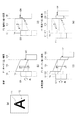
図1は、本実施例の光電変換装置の全体の回路構成と、上部電極101の配置レイアウトとを合わせて示した図である。
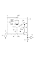
図2は、m列目およびm+1列目の列回路140の等価回路を示した図である。図2の列回路140は、図1に示した列回路140のうちの2列に対応する。
図3(a)は、光電変換装置の画素100の等価回路と、光電変換部120の模式図とを合わせて示した図である。図3(b)は、光電変換部120の等価回路を示した図である。
上述した図3(a)、図3(b)の光電変換部120の具体的な構成について詳細に説明する。
次に、本実施例の光電変換装置の平面構造、断面構造について説明する。
次に、本実施例における画素100の動作、ならびに、第1ブロッキング層104、光電変換層103、第2ブロッキング層102の機能について詳しく説明する。
図8は、本実施形態の光電変換装置に用いられるグローバルシャッター動作における駆動信号のタイミングチャートを示している。図8には、簡単のためn行目とn+1行目の2行分の信号読み出し動作に対応した駆動信号が示されている。
図9(a)〜図9(e)のそれぞれを用いて、本実施例の効果を説明する。図9(b)、図9(c)は参考例であって、光電変換部120が第1ブロッキング層104を有しない例を示している。図9(d)、図9(e)は、これまでに述べてきた、光電変換部120が第1ブロッキング層104を有する例を示している。ただしここでは信号電荷として電子を利用する(電子蓄積型)場合で説明する。正孔を利用する場合も同様の効果がある。
以下図面を用いて本発明における容量素子109と電圧制御部110の機能について詳述する。
本実施例について、実施例1と異なる点を中心に説明する。
本実施例の光電変換装置について、実施例2と異なる点を中心に説明する。
本実施例の光電変換装置について、実施例1と異なる点を中心に説明する。
本実施例の光電変換装置について、実施例1と異なる点を中心に説明する。
本発明に係る撮像システムの実施例について説明する。撮像システムとして、デジタルスチルカメラ、デジタルカムコーダ、カメラヘッド、複写機、ファックス、携帯電話、車載カメラ、観測衛星などがあげられる。図22に、撮像システムの例としてデジタルスチルカメラのブロック図を示す。
図23(A)は、車載カメラに関する撮像システムの一例を示したものである。撮像システム1000は、上述した各実施例の光電変換装置を撮像装置1010として備える撮像システムである。撮像システム1000は、撮像装置1010により取得された複数の画像データに対し、画像処理を行う画像処理部1030と、撮像システム1000により取得された複数の画像データから視差(視差画像の位相差)の取得を行う視差取得部1040を有する。
106 増幅トランジスタ
107 選択トランジスタ(トランジスタの一例)
108 リセットトランジスタ(トランジスタの一例)
109 容量素子
110 電圧供給部
120 光電変換部
132 vRES線(同一の配線の一例)
134 pSEL線(同一の配線の一例)
Claims (14)
- 半導体基板と、画素とを備え、
前記画素は、
第1電極と、前記第1電極および前記半導体基板の間に配された第2電極と、前記第1電極および前記第2電極の間に配された光電変換層とを含む光電変換部と、
増幅トランジスタと、
前記第2電極と前記増幅トランジスタのゲートに接続された不純物拡散部と、
オンすることによって、前記不純物拡散部の電圧をリセットするトランジスタと、
第1ノードと第2ノードとを備え、前記第1ノードに前記不純物拡散部に接続された容量素子とを有する光電変換装置であって、
前記光電変換装置は、同一の配線を介して前記第2ノードおよび前記トランジスタに接続されるとともに、値の異なる複数の電圧を前記同一の配線に出力する電圧制御部を有することを特徴とする光電変換装置。 - 前記画素が複数行および複数列に渡って配され、
前記複数の電圧が前記トランジスタを介して前記不純物拡散部に入力されることによって、前記増幅トランジスタのオンとオフが切り替わることを特徴とする請求項1に記載の光電変換装置。 - 前記光電変換層の蓄積期間において、前記電圧制御部は前記同一の配線に、第1電圧を供給し、
前記増幅トランジスタが信号を出力する期間において、前記電圧制御部は前記同一の配線に、前記第1電圧とは値の異なる電圧である第2電圧を供給し、
前記第1電圧が、前記増幅トランジスタがオフの状態となる電圧であることを特徴とする請求項2に記載の光電変換装置。 - 半導体基板と、画素と、出力線とを備え、
前記画素は、
第1電極と、前記第1電極および前記半導体基板の間に配された第2電極と、前記第1電極および前記第2電極の間に配された光電変換層とを含む光電変換部と、
増幅トランジスタと、
前記第2電極と前記増幅トランジスタのゲートに接続された不純物拡散部と、
オンすることによって、前記増幅トランジスタと前記出力線との間の電気的経路を導通させるトランジスタと、
第1ノードと第2ノードとを備え、前記第1ノードに前記不純物拡散部に接続された容量素子とを有する光電変換装置であって、
前記光電変換装置は、同一の配線を介して前記第2ノードおよび前記トランジスタのゲートに接続されるとともに、値の異なる複数の電圧を前記同一の配線に出力する電圧制御部を有することを特徴とする光電変換装置。 - 前記光電変換層の蓄積期間において、前記電圧制御部は前記同一の配線に、第1電圧を供給し、
前記増幅トランジスタが信号を出力する期間において、前記電圧制御部は前記同一の配線に、前記第1電圧とは値の異なる電圧である第2電圧を供給することを特徴とする請求項1〜4のいずれか1項に記載の光電変換装置。 - 前記光電変換層の蓄積期間において、前記電圧制御部は前記同一の配線に、第1電圧を供給し、
前記増幅トランジスタが信号を出力する期間において、前記電圧制御部は前記同一の配線に、前記第1電圧とは値の異なる電圧である第2電圧を供給することを特徴とする請求項1〜5のいずれか1項に記載の光電変換装置。 - 前記不純物拡散部は、所定の電圧が与えられる半導体領域に接して形成され、
前記第1電圧が、前記所定の電圧と略等しい電圧であることを特徴とする請求項5または6に記載の光電変換装置。 - 前記光電変換層の電荷が、前記第2電極を介して前記不純物拡散部に蓄積されることを特徴とする請求項1〜7のいずれか1項に記載の光電変換装置。
- 前記光電変換部は、前記光電変換層と前記第2電極との間にブロッキング層を有し、
前記ブロッキング層は、蓄積期間中に前記光電変換層が前記第2電極に出力する電荷とは反対の極性の電荷の、前記第2電極から前記光電変換層への注入を抑制することを特徴とする請求項8に記載の光電変換装置。 - 前記光電変換部は、前記光電変換層と前記第2電極との間に絶縁層を有し、
前記光電変換層が蓄積する電荷に対応する電圧が、前記第2電極に出力されることを特徴とする請求項1〜7のいずれか1項に記載の光電変換装置。 - 半導体基板と、画素とを備え、
前記画素は、
第1電極と、前記第1電極および前記半導体基板の間に配された第2電極と、前記第1電極および前記第2電極の間に配された光電変換層とを含む光電変換部と、
増幅トランジスタと、
前記第2電極と前記増幅トランジスタのゲートに接続された不純物拡散部と、
トランジスタと、
第1ノードと第2ノードとを備え、前記第1ノードに前記不純物拡散部に接続された容量素子とを有する光電変換装置であって、
前記光電変換装置は、値の異なる複数の電圧を前記第2ノードに出力する電圧制御部を有し、
前記複数の電圧によって、前記増幅トランジスタのオンとオフが変更されることを特徴とする光電変換装置。 - 請求項1〜11のいずれか1項に記載の光電変換装置と、
前記光電変換装置が出力する信号を用いて画像を生成する信号処理部とを有することを特徴とする撮像システム。 - 前記画素は、1つのマイクロレンズと、前記1つのマイクロレンズに対応して配された複数の前記光電変換部を有し、
前記信号処理部は、前記複数の光電変換部の一部が生成した電荷に基づく信号と、前記複数の光電変換部の他の一部が生成した電荷に基づく信号とを用いて、被写体の距離情報を生成することを特徴とする請求項12に記載の撮像システム。 - 移動体であって、
請求項1〜11のいずれか1項に記載の光電変換装置と、
前記光電変換装置からの信号に基づいて、対象物までの距離情報を取得する距離情報取得手段と、
前記距離情報に基づいて前記移動体を制御する制御手段と、を有することを特徴とする移動体。
Priority Applications (2)
| Application Number | Priority Date | Filing Date | Title |
|---|---|---|---|
| JP2016254364A JP2018107725A (ja) | 2016-12-27 | 2016-12-27 | 光電変換装置、撮像システム |
| US15/845,995 US10728471B2 (en) | 2016-12-27 | 2017-12-18 | Photoelectric conversion device with a voltage control unit connected to a reset transistor and a capacitive element, and associated imaging system |
Applications Claiming Priority (1)
| Application Number | Priority Date | Filing Date | Title |
|---|---|---|---|
| JP2016254364A JP2018107725A (ja) | 2016-12-27 | 2016-12-27 | 光電変換装置、撮像システム |
Publications (2)
| Publication Number | Publication Date |
|---|---|
| JP2018107725A true JP2018107725A (ja) | 2018-07-05 |
| JP2018107725A5 JP2018107725A5 (ja) | 2020-02-06 |
Family
ID=62630581
Family Applications (1)
| Application Number | Title | Priority Date | Filing Date |
|---|---|---|---|
| JP2016254364A Pending JP2018107725A (ja) | 2016-12-27 | 2016-12-27 | 光電変換装置、撮像システム |
Country Status (2)
| Country | Link |
|---|---|
| US (1) | US10728471B2 (ja) |
| JP (1) | JP2018107725A (ja) |
Cited By (1)
| Publication number | Priority date | Publication date | Assignee | Title |
|---|---|---|---|---|
| JP2021125492A (ja) * | 2020-01-31 | 2021-08-30 | キヤノン株式会社 | 半導体装置、表示装置、撮像システム及び移動体 |
Families Citing this family (2)
| Publication number | Priority date | Publication date | Assignee | Title |
|---|---|---|---|---|
| JP2018093297A (ja) * | 2016-11-30 | 2018-06-14 | キヤノン株式会社 | 光電変換装置、撮像システム |
| JP2018182021A (ja) | 2017-04-11 | 2018-11-15 | ソニーセミコンダクタソリューションズ株式会社 | 撮像素子、積層型撮像素子及び固体撮像装置 |
Citations (5)
| Publication number | Priority date | Publication date | Assignee | Title |
|---|---|---|---|---|
| JPH11112018A (ja) * | 1997-10-06 | 1999-04-23 | Canon Inc | 固体撮像装置と信号検出装置と信号蓄積装置 |
| JP2012119652A (ja) * | 2010-03-17 | 2012-06-21 | Fujifilm Corp | 有機光電変換素子の製造方法、有機光電変換素子、撮像素子、撮像装置 |
| JP2016033981A (ja) * | 2014-07-31 | 2016-03-10 | キヤノン株式会社 | 固体撮像素子および撮像システム |
| JP2016052132A (ja) * | 2015-09-18 | 2016-04-11 | 株式会社ニコン | 撮像装置 |
| US20160190188A1 (en) * | 2014-12-26 | 2016-06-30 | Panasonic Intellectual Property Management Co., Ltd. | Imaging device including unit pixel cell |
Family Cites Families (25)
| Publication number | Priority date | Publication date | Assignee | Title |
|---|---|---|---|---|
| US7446807B2 (en) * | 2004-12-03 | 2008-11-04 | Micron Technology, Inc. | Imager pixel with capacitance for boosting reset voltage |
| US20070035649A1 (en) * | 2005-08-10 | 2007-02-15 | Micron Technology, Inc. | Image pixel reset through dual conversion gain gate |
| JPWO2011058684A1 (ja) * | 2009-11-12 | 2013-03-28 | パナソニック株式会社 | 固体撮像装置 |
| JP2013030820A (ja) | 2009-11-12 | 2013-02-07 | Panasonic Corp | 固体撮像装置 |
| WO2013179597A1 (ja) * | 2012-05-30 | 2013-12-05 | パナソニック株式会社 | 固体撮像装置、その駆動方法及び撮影装置 |
| GB2516971A (en) * | 2013-08-09 | 2015-02-11 | St Microelectronics Res & Dev | A Pixel |
| GB201318404D0 (en) * | 2013-10-17 | 2013-12-04 | Cmosis Nv | An image sensor |
| JP6260787B2 (ja) * | 2014-05-23 | 2018-01-17 | パナソニックIpマネジメント株式会社 | 撮像装置 |
| JP2016021445A (ja) * | 2014-07-11 | 2016-02-04 | キヤノン株式会社 | 光電変換装置、および、撮像システム |
| JP6389685B2 (ja) * | 2014-07-30 | 2018-09-12 | キヤノン株式会社 | 撮像装置、および、撮像システム |
| JP6425448B2 (ja) * | 2014-07-31 | 2018-11-21 | キヤノン株式会社 | 光電変換装置、および、撮像システム |
| JP6521586B2 (ja) * | 2014-07-31 | 2019-05-29 | キヤノン株式会社 | 固体撮像素子および撮像システム |
| US10212372B2 (en) * | 2014-12-26 | 2019-02-19 | Panasonic Intellectual Property Management Co., Ltd. | Imaging device including signal line and unit pixel cell including charge storage region |
| JP6390856B2 (ja) | 2014-12-26 | 2018-09-19 | パナソニックIpマネジメント株式会社 | 撮像装置 |
| WO2016121521A1 (ja) * | 2015-01-29 | 2016-08-04 | ソニー株式会社 | 固体撮像素子および電子機器 |
| JP6562243B2 (ja) | 2015-02-17 | 2019-08-21 | パナソニックIpマネジメント株式会社 | 撮像装置 |
| JP6555468B2 (ja) * | 2015-04-02 | 2019-08-07 | パナソニックIpマネジメント株式会社 | 撮像装置 |
| JP2017098809A (ja) * | 2015-11-26 | 2017-06-01 | キヤノン株式会社 | 光電変換装置、および、撮像システム |
| JP6808316B2 (ja) * | 2015-12-04 | 2021-01-06 | キヤノン株式会社 | 撮像装置、および、撮像システム |
| DE102016122658B4 (de) * | 2015-12-04 | 2021-07-15 | Canon Kabushiki Kaisha | Abbildungsvorrichtung und Abbildungssystem |
| JP6903896B2 (ja) * | 2016-01-13 | 2021-07-14 | ソニーグループ株式会社 | 受光素子の製造方法 |
| JP6727831B2 (ja) * | 2016-02-09 | 2020-07-22 | キヤノン株式会社 | 光電変換装置、および、撮像システム |
| JP2017152669A (ja) * | 2016-02-25 | 2017-08-31 | パナソニックIpマネジメント株式会社 | 撮像装置 |
| JP2018093297A (ja) * | 2016-11-30 | 2018-06-14 | キヤノン株式会社 | 光電変換装置、撮像システム |
| JP6808463B2 (ja) * | 2016-11-30 | 2021-01-06 | キヤノン株式会社 | 光電変換装置および光電変換システム |
-
2016
- 2016-12-27 JP JP2016254364A patent/JP2018107725A/ja active Pending
-
2017
- 2017-12-18 US US15/845,995 patent/US10728471B2/en active Active
Patent Citations (5)
| Publication number | Priority date | Publication date | Assignee | Title |
|---|---|---|---|---|
| JPH11112018A (ja) * | 1997-10-06 | 1999-04-23 | Canon Inc | 固体撮像装置と信号検出装置と信号蓄積装置 |
| JP2012119652A (ja) * | 2010-03-17 | 2012-06-21 | Fujifilm Corp | 有機光電変換素子の製造方法、有機光電変換素子、撮像素子、撮像装置 |
| JP2016033981A (ja) * | 2014-07-31 | 2016-03-10 | キヤノン株式会社 | 固体撮像素子および撮像システム |
| US20160190188A1 (en) * | 2014-12-26 | 2016-06-30 | Panasonic Intellectual Property Management Co., Ltd. | Imaging device including unit pixel cell |
| JP2016052132A (ja) * | 2015-09-18 | 2016-04-11 | 株式会社ニコン | 撮像装置 |
Cited By (1)
| Publication number | Priority date | Publication date | Assignee | Title |
|---|---|---|---|---|
| JP2021125492A (ja) * | 2020-01-31 | 2021-08-30 | キヤノン株式会社 | 半導体装置、表示装置、撮像システム及び移動体 |
Also Published As
| Publication number | Publication date |
|---|---|
| US10728471B2 (en) | 2020-07-28 |
| US20180184017A1 (en) | 2018-06-28 |
Similar Documents
| Publication | Publication Date | Title |
|---|---|---|
| US9722107B2 (en) | Photoelectric conversion device and imaging system | |
| US9826181B2 (en) | Photoelectric conversion device and imaging system | |
| JP6501462B2 (ja) | 光電変換装置及び光電変換装置の駆動方法 | |
| US10419695B2 (en) | Photoelectric conversion device, imaging system, and mobile apparatus | |
| US9941315B2 (en) | Photoelectric conversion device and imaging system | |
| WO2017138273A1 (en) | Photoelectric conversion apparatus and imaging system | |
| JP7000020B2 (ja) | 光電変換装置、撮像システム | |
| US11405570B2 (en) | Imaging device, imaging system, and semiconductor chip | |
| PH12016000416A1 (en) | Image pickup device and image pickup system | |
| US10944931B2 (en) | Solid state imaging device and imaging system | |
| US9866774B2 (en) | Photoelectric conversion device and imaging system | |
| JP7395300B2 (ja) | 光電変換装置、光電変換システム、および移動体 | |
| US10368016B2 (en) | Photoelectric conversion device and imaging system | |
| US20180151760A1 (en) | Photoelectric conversion device, drive method of photoelectric conversion device, and imaging system | |
| US10728471B2 (en) | Photoelectric conversion device with a voltage control unit connected to a reset transistor and a capacitive element, and associated imaging system | |
| JP6494207B2 (ja) | 光電変換装置、光電変換システム、光電変換装置の駆動方法 | |
| JP7224823B2 (ja) | 光検出装置 | |
| JP7027175B2 (ja) | 半導体装置および機器 | |
| JP2020191600A (ja) | 光電変換装置および光電変換システム | |
| JP6894760B2 (ja) | 光電変換装置及び撮像システム | |
| US20230387173A1 (en) | Photoelectric conversion device having expanded dynamic range and transfer electrodes | |
| JP2022138487A (ja) | 光電変換装置 | |
| JP2018142937A (ja) | 光電変換装置、撮像システム、移動体 |
Legal Events
| Date | Code | Title | Description |
|---|---|---|---|
| A521 | Request for written amendment filed |
Free format text: JAPANESE INTERMEDIATE CODE: A523 Effective date: 20191213 |
|
| A621 | Written request for application examination |
Free format text: JAPANESE INTERMEDIATE CODE: A621 Effective date: 20191213 |
|
| A977 | Report on retrieval |
Free format text: JAPANESE INTERMEDIATE CODE: A971007 Effective date: 20200824 |
|
| A131 | Notification of reasons for refusal |
Free format text: JAPANESE INTERMEDIATE CODE: A131 Effective date: 20200901 |
|
| A02 | Decision of refusal |
Free format text: JAPANESE INTERMEDIATE CODE: A02 Effective date: 20210309 |