JP2018107725A - Photoelectric conversion device and imaging system - Google Patents
Photoelectric conversion device and imaging system Download PDFInfo
- Publication number
- JP2018107725A JP2018107725A JP2016254364A JP2016254364A JP2018107725A JP 2018107725 A JP2018107725 A JP 2018107725A JP 2016254364 A JP2016254364 A JP 2016254364A JP 2016254364 A JP2016254364 A JP 2016254364A JP 2018107725 A JP2018107725 A JP 2018107725A
- Authority
- JP
- Japan
- Prior art keywords
- photoelectric conversion
- voltage
- electrode
- signal
- node
- Prior art date
- Legal status (The legal status is an assumption and is not a legal conclusion. Google has not performed a legal analysis and makes no representation as to the accuracy of the status listed.)
- Pending
Links
- 238000006243 chemical reaction Methods 0.000 title claims abstract description 352
- 238000003384 imaging method Methods 0.000 title claims description 58
- 230000000903 blocking effect Effects 0.000 claims description 75
- 239000004065 semiconductor Substances 0.000 claims description 74
- 230000003321 amplification Effects 0.000 claims description 55
- 238000003199 nucleic acid amplification method Methods 0.000 claims description 55
- 239000000758 substrate Substances 0.000 claims description 35
- 239000012535 impurity Substances 0.000 claims description 34
- 238000009792 diffusion process Methods 0.000 claims description 29
- 238000012545 processing Methods 0.000 claims description 17
- 238000009825 accumulation Methods 0.000 claims description 16
- 238000002347 injection Methods 0.000 claims description 12
- 239000007924 injection Substances 0.000 claims description 12
- 239000010410 layer Substances 0.000 description 193
- 239000003990 capacitor Substances 0.000 description 46
- 239000000463 material Substances 0.000 description 33
- 238000010586 diagram Methods 0.000 description 28
- 230000003287 optical effect Effects 0.000 description 26
- 230000008859 change Effects 0.000 description 16
- 230000007423 decrease Effects 0.000 description 9
- 230000000694 effects Effects 0.000 description 8
- 230000006870 function Effects 0.000 description 8
- 150000001875 compounds Chemical class 0.000 description 5
- 229910021417 amorphous silicon Inorganic materials 0.000 description 4
- 239000010408 film Substances 0.000 description 4
- 229910052751 metal Inorganic materials 0.000 description 4
- 239000002184 metal Substances 0.000 description 4
- 238000000034 method Methods 0.000 description 4
- 230000008569 process Effects 0.000 description 4
- 238000005096 rolling process Methods 0.000 description 4
- 230000035945 sensitivity Effects 0.000 description 4
- XUIMIQQOPSSXEZ-UHFFFAOYSA-N Silicon Chemical compound [Si] XUIMIQQOPSSXEZ-UHFFFAOYSA-N 0.000 description 3
- 238000004364 calculation method Methods 0.000 description 3
- 239000011159 matrix material Substances 0.000 description 3
- 239000002096 quantum dot Substances 0.000 description 3
- 230000009467 reduction Effects 0.000 description 3
- 230000000630 rising effect Effects 0.000 description 3
- 229910052710 silicon Inorganic materials 0.000 description 3
- 239000010703 silicon Substances 0.000 description 3
- 238000012546 transfer Methods 0.000 description 3
- JBRZTFJDHDCESZ-UHFFFAOYSA-N AsGa Chemical compound [As]#[Ga] JBRZTFJDHDCESZ-UHFFFAOYSA-N 0.000 description 2
- 229910001218 Gallium arsenide Inorganic materials 0.000 description 2
- 230000004888 barrier function Effects 0.000 description 2
- VYXSBFYARXAAKO-WTKGSRSZSA-N chembl402140 Chemical compound Cl.C1=2C=C(C)C(NCC)=CC=2OC2=C\C(=N/CC)C(C)=CC2=C1C1=CC=CC=C1C(=O)OCC VYXSBFYARXAAKO-WTKGSRSZSA-N 0.000 description 2
- 230000003247 decreasing effect Effects 0.000 description 2
- 230000007547 defect Effects 0.000 description 2
- 238000007599 discharging Methods 0.000 description 2
- 238000004519 manufacturing process Methods 0.000 description 2
- 239000002245 particle Substances 0.000 description 2
- IEQIEDJGQAUEQZ-UHFFFAOYSA-N phthalocyanine Chemical compound N1C(N=C2C3=CC=CC=C3C(N=C3C4=CC=CC=C4C(=N4)N3)=N2)=C(C=CC=C2)C2=C1N=C1C2=CC=CC=C2C4=N1 IEQIEDJGQAUEQZ-UHFFFAOYSA-N 0.000 description 2
- 229910017115 AlSb Inorganic materials 0.000 description 1
- XMWRBQBLMFGWIX-UHFFFAOYSA-N C60 fullerene Chemical compound C12=C3C(C4=C56)=C7C8=C5C5=C9C%10=C6C6=C4C1=C1C4=C6C6=C%10C%10=C9C9=C%11C5=C8C5=C8C7=C3C3=C7C2=C1C1=C2C4=C6C4=C%10C6=C9C9=C%11C5=C5C8=C3C3=C7C1=C1C2=C4C6=C2C9=C5C3=C12 XMWRBQBLMFGWIX-UHFFFAOYSA-N 0.000 description 1
- 229910005540 GaP Inorganic materials 0.000 description 1
- NRCMAYZCPIVABH-UHFFFAOYSA-N Quinacridone Chemical compound N1C2=CC=CC=C2C(=O)C2=C1C=C1C(=O)C3=CC=CC=C3NC1=C2 NRCMAYZCPIVABH-UHFFFAOYSA-N 0.000 description 1
- 229910010421 TiNx Inorganic materials 0.000 description 1
- ATJFFYVFTNAWJD-UHFFFAOYSA-N Tin Chemical compound [Sn] ATJFFYVFTNAWJD-UHFFFAOYSA-N 0.000 description 1
- HCHKCACWOHOZIP-UHFFFAOYSA-N Zinc Chemical compound [Zn] HCHKCACWOHOZIP-UHFFFAOYSA-N 0.000 description 1
- 230000005540 biological transmission Effects 0.000 description 1
- UHYPYGJEEGLRJD-UHFFFAOYSA-N cadmium(2+);selenium(2-) Chemical compound [Se-2].[Cd+2] UHYPYGJEEGLRJD-UHFFFAOYSA-N 0.000 description 1
- 239000000969 carrier Substances 0.000 description 1
- 238000007906 compression Methods 0.000 description 1
- 230000006835 compression Effects 0.000 description 1
- 238000012937 correction Methods 0.000 description 1
- VBVAVBCYMYWNOU-UHFFFAOYSA-N coumarin 6 Chemical compound C1=CC=C2SC(C3=CC4=CC=C(C=C4OC3=O)N(CC)CC)=NC2=C1 VBVAVBCYMYWNOU-UHFFFAOYSA-N 0.000 description 1
- 230000008034 disappearance Effects 0.000 description 1
- 239000003574 free electron Substances 0.000 description 1
- 229910003472 fullerene Inorganic materials 0.000 description 1
- 229910052732 germanium Inorganic materials 0.000 description 1
- GNPVGFCGXDBREM-UHFFFAOYSA-N germanium atom Chemical compound [Ge] GNPVGFCGXDBREM-UHFFFAOYSA-N 0.000 description 1
- 229910052738 indium Inorganic materials 0.000 description 1
- APFVFJFRJDLVQX-UHFFFAOYSA-N indium atom Chemical compound [In] APFVFJFRJDLVQX-UHFFFAOYSA-N 0.000 description 1
- 239000011229 interlayer Substances 0.000 description 1
- 239000000203 mixture Substances 0.000 description 1
- 238000012986 modification Methods 0.000 description 1
- 230000004048 modification Effects 0.000 description 1
- LKKPNUDVOYAOBB-UHFFFAOYSA-N naphthalocyanine Chemical compound N1C(N=C2C3=CC4=CC=CC=C4C=C3C(N=C3C4=CC5=CC=CC=C5C=C4C(=N4)N3)=N2)=C(C=C2C(C=CC=C2)=C2)C2=C1N=C1C2=CC3=CC=CC=C3C=C2C4=N1 LKKPNUDVOYAOBB-UHFFFAOYSA-N 0.000 description 1
- 230000003071 parasitic effect Effects 0.000 description 1
- 229910021420 polycrystalline silicon Inorganic materials 0.000 description 1
- 229920005591 polysilicon Polymers 0.000 description 1
- 238000005036 potential barrier Methods 0.000 description 1
- 230000006798 recombination Effects 0.000 description 1
- 238000005215 recombination Methods 0.000 description 1
- 230000004044 response Effects 0.000 description 1
- 238000003860 storage Methods 0.000 description 1
- 239000010409 thin film Substances 0.000 description 1
- 229910052725 zinc Inorganic materials 0.000 description 1
- 239000011701 zinc Substances 0.000 description 1
Images


Classifications
-
- H—ELECTRICITY
- H04—ELECTRIC COMMUNICATION TECHNIQUE
- H04N—PICTORIAL COMMUNICATION, e.g. TELEVISION
- H04N25/00—Circuitry of solid-state image sensors [SSIS]; Control thereof
- H04N25/40—Extracting pixel data from image sensors by controlling scanning circuits, e.g. by modifying the number of pixels sampled or to be sampled
- H04N25/44—Extracting pixel data from image sensors by controlling scanning circuits, e.g. by modifying the number of pixels sampled or to be sampled by partially reading an SSIS array
-
- G—PHYSICS
- G01—MEASURING; TESTING
- G01C—MEASURING DISTANCES, LEVELS OR BEARINGS; SURVEYING; NAVIGATION; GYROSCOPIC INSTRUMENTS; PHOTOGRAMMETRY OR VIDEOGRAMMETRY
- G01C3/00—Measuring distances in line of sight; Optical rangefinders
- G01C3/02—Details
- G01C3/06—Use of electric means to obtain final indication
- G01C3/08—Use of electric radiation detectors
- G01C3/085—Use of electric radiation detectors with electronic parallax measurement
-
- H—ELECTRICITY
- H01—ELECTRIC ELEMENTS
- H01L—SEMICONDUCTOR DEVICES NOT COVERED BY CLASS H10
- H01L27/00—Devices consisting of a plurality of semiconductor or other solid-state components formed in or on a common substrate
- H01L27/14—Devices consisting of a plurality of semiconductor or other solid-state components formed in or on a common substrate including semiconductor components sensitive to infrared radiation, light, electromagnetic radiation of shorter wavelength or corpuscular radiation and specially adapted either for the conversion of the energy of such radiation into electrical energy or for the control of electrical energy by such radiation
- H01L27/144—Devices controlled by radiation
- H01L27/146—Imager structures
- H01L27/14601—Structural or functional details thereof
- H01L27/14609—Pixel-elements with integrated switching, control, storage or amplification elements
- H01L27/1461—Pixel-elements with integrated switching, control, storage or amplification elements characterised by the photosensitive area
-
- H—ELECTRICITY
- H01—ELECTRIC ELEMENTS
- H01L—SEMICONDUCTOR DEVICES NOT COVERED BY CLASS H10
- H01L27/00—Devices consisting of a plurality of semiconductor or other solid-state components formed in or on a common substrate
- H01L27/14—Devices consisting of a plurality of semiconductor or other solid-state components formed in or on a common substrate including semiconductor components sensitive to infrared radiation, light, electromagnetic radiation of shorter wavelength or corpuscular radiation and specially adapted either for the conversion of the energy of such radiation into electrical energy or for the control of electrical energy by such radiation
- H01L27/144—Devices controlled by radiation
- H01L27/146—Imager structures
- H01L27/14601—Structural or functional details thereof
- H01L27/14609—Pixel-elements with integrated switching, control, storage or amplification elements
- H01L27/14612—Pixel-elements with integrated switching, control, storage or amplification elements involving a transistor
-
- H—ELECTRICITY
- H01—ELECTRIC ELEMENTS
- H01L—SEMICONDUCTOR DEVICES NOT COVERED BY CLASS H10
- H01L27/00—Devices consisting of a plurality of semiconductor or other solid-state components formed in or on a common substrate
- H01L27/14—Devices consisting of a plurality of semiconductor or other solid-state components formed in or on a common substrate including semiconductor components sensitive to infrared radiation, light, electromagnetic radiation of shorter wavelength or corpuscular radiation and specially adapted either for the conversion of the energy of such radiation into electrical energy or for the control of electrical energy by such radiation
- H01L27/144—Devices controlled by radiation
- H01L27/146—Imager structures
- H01L27/14601—Structural or functional details thereof
- H01L27/14625—Optical elements or arrangements associated with the device
- H01L27/14627—Microlenses
-
- H—ELECTRICITY
- H01—ELECTRIC ELEMENTS
- H01L—SEMICONDUCTOR DEVICES NOT COVERED BY CLASS H10
- H01L27/00—Devices consisting of a plurality of semiconductor or other solid-state components formed in or on a common substrate
- H01L27/14—Devices consisting of a plurality of semiconductor or other solid-state components formed in or on a common substrate including semiconductor components sensitive to infrared radiation, light, electromagnetic radiation of shorter wavelength or corpuscular radiation and specially adapted either for the conversion of the energy of such radiation into electrical energy or for the control of electrical energy by such radiation
- H01L27/144—Devices controlled by radiation
- H01L27/146—Imager structures
- H01L27/14601—Structural or functional details thereof
- H01L27/14636—Interconnect structures
-
- H—ELECTRICITY
- H01—ELECTRIC ELEMENTS
- H01L—SEMICONDUCTOR DEVICES NOT COVERED BY CLASS H10
- H01L27/00—Devices consisting of a plurality of semiconductor or other solid-state components formed in or on a common substrate
- H01L27/14—Devices consisting of a plurality of semiconductor or other solid-state components formed in or on a common substrate including semiconductor components sensitive to infrared radiation, light, electromagnetic radiation of shorter wavelength or corpuscular radiation and specially adapted either for the conversion of the energy of such radiation into electrical energy or for the control of electrical energy by such radiation
- H01L27/144—Devices controlled by radiation
- H01L27/146—Imager structures
- H01L27/14643—Photodiode arrays; MOS imagers
-
- H—ELECTRICITY
- H04—ELECTRIC COMMUNICATION TECHNIQUE
- H04N—PICTORIAL COMMUNICATION, e.g. TELEVISION
- H04N25/00—Circuitry of solid-state image sensors [SSIS]; Control thereof
- H04N25/50—Control of the SSIS exposure
- H04N25/53—Control of the integration time
-
- H—ELECTRICITY
- H04—ELECTRIC COMMUNICATION TECHNIQUE
- H04N—PICTORIAL COMMUNICATION, e.g. TELEVISION
- H04N25/00—Circuitry of solid-state image sensors [SSIS]; Control thereof
- H04N25/70—SSIS architectures; Circuits associated therewith
- H04N25/71—Charge-coupled device [CCD] sensors; Charge-transfer registers specially adapted for CCD sensors
- H04N25/75—Circuitry for providing, modifying or processing image signals from the pixel array
-
- H—ELECTRICITY
- H04—ELECTRIC COMMUNICATION TECHNIQUE
- H04N—PICTORIAL COMMUNICATION, e.g. TELEVISION
- H04N25/00—Circuitry of solid-state image sensors [SSIS]; Control thereof
- H04N25/70—SSIS architectures; Circuits associated therewith
- H04N25/76—Addressed sensors, e.g. MOS or CMOS sensors
-
- H—ELECTRICITY
- H04—ELECTRIC COMMUNICATION TECHNIQUE
- H04N—PICTORIAL COMMUNICATION, e.g. TELEVISION
- H04N25/00—Circuitry of solid-state image sensors [SSIS]; Control thereof
- H04N25/70—SSIS architectures; Circuits associated therewith
- H04N25/76—Addressed sensors, e.g. MOS or CMOS sensors
- H04N25/77—Pixel circuitry, e.g. memories, A/D converters, pixel amplifiers, shared circuits or shared components
- H04N25/778—Pixel circuitry, e.g. memories, A/D converters, pixel amplifiers, shared circuits or shared components comprising amplifiers shared between a plurality of pixels, i.e. at least one part of the amplifier must be on the sensor array itself
-
- B—PERFORMING OPERATIONS; TRANSPORTING
- B60—VEHICLES IN GENERAL
- B60W—CONJOINT CONTROL OF VEHICLE SUB-UNITS OF DIFFERENT TYPE OR DIFFERENT FUNCTION; CONTROL SYSTEMS SPECIALLY ADAPTED FOR HYBRID VEHICLES; ROAD VEHICLE DRIVE CONTROL SYSTEMS FOR PURPOSES NOT RELATED TO THE CONTROL OF A PARTICULAR SUB-UNIT
- B60W2420/00—Indexing codes relating to the type of sensors based on the principle of their operation
- B60W2420/40—Photo or light sensitive means, e.g. infrared sensors
- B60W2420/403—Image sensing, e.g. optical camera
-
- B—PERFORMING OPERATIONS; TRANSPORTING
- B60—VEHICLES IN GENERAL
- B60W—CONJOINT CONTROL OF VEHICLE SUB-UNITS OF DIFFERENT TYPE OR DIFFERENT FUNCTION; CONTROL SYSTEMS SPECIALLY ADAPTED FOR HYBRID VEHICLES; ROAD VEHICLE DRIVE CONTROL SYSTEMS FOR PURPOSES NOT RELATED TO THE CONTROL OF A PARTICULAR SUB-UNIT
- B60W2554/00—Input parameters relating to objects
-
- B—PERFORMING OPERATIONS; TRANSPORTING
- B60—VEHICLES IN GENERAL
- B60W—CONJOINT CONTROL OF VEHICLE SUB-UNITS OF DIFFERENT TYPE OR DIFFERENT FUNCTION; CONTROL SYSTEMS SPECIALLY ADAPTED FOR HYBRID VEHICLES; ROAD VEHICLE DRIVE CONTROL SYSTEMS FOR PURPOSES NOT RELATED TO THE CONTROL OF A PARTICULAR SUB-UNIT
- B60W30/00—Purposes of road vehicle drive control systems not related to the control of a particular sub-unit, e.g. of systems using conjoint control of vehicle sub-units, or advanced driver assistance systems for ensuring comfort, stability and safety or drive control systems for propelling or retarding the vehicle
- B60W30/08—Active safety systems predicting or avoiding probable or impending collision or attempting to minimise its consequences
- B60W30/09—Taking automatic action to avoid collision, e.g. braking and steering
Abstract
Description
本発明は、光電変換装置、撮像システムに関する。 The present invention relates to a photoelectric conversion device and an imaging system.
カメラのイメージセンサ等に用いられる光電変換装置として、積層型の光電変換装置が提案されている。特許文献1に記載の光電変換装置では、半導体基板に光電変換層が積層されている。光電変換層から見て入射面側には上部電極が配されている。一方、光電変換層から見て半導体基板側には画素電極が配されている。特許文献1には、リセットトランジスタとリセット制御容量を用いて、画素電極のリセット電圧を制御することが記載されている。
As a photoelectric conversion device used for an image sensor or the like of a camera, a stacked photoelectric conversion device has been proposed. In the photoelectric conversion device described in
特許文献1に記載の光電変換装置では、画素を駆動するためのトランジスタに接続される配線とは別に、リセット制御容量を制御する制御線を設けているため、画素領域の回路面積が増大していた。
In the photoelectric conversion device described in
本発明は上記の課題を鑑みて為されたものであり、その一の態様は、半導体基板と、画素とを備え、前記画素は、第1電極と、前記第1電極および前記半導体基板の間に配された第2電極と、前記第1電極および前記第2電極の間に配された光電変換層とを含む光電変換部と、増幅トランジスタと、前記第2電極と前記増幅トランジスタのゲートに接続された不純物拡散部と、オンすることによって、前記不純物拡散部の電圧をリセットするトランジスタと、第1ノードと第2ノードとを備え、前記第1ノードに前記不純物拡散部に接続された容量素子とを有する光電変換装置であって、前記光電変換装置は、同一の配線を介して前記第2ノードおよび前記トランジスタに接続されるとともに、値の異なる複数の電圧を前記同一の配線に出力する電圧制御部を有することを特徴とする光電変換装置である。 The present invention has been made in view of the above problems, and one aspect thereof includes a semiconductor substrate and a pixel, and the pixel is between the first electrode, the first electrode, and the semiconductor substrate. A photoelectric conversion unit including a second electrode disposed on the first electrode, a photoelectric conversion layer disposed between the first electrode and the second electrode, an amplification transistor, and a gate of the second electrode and the amplification transistor. A capacitor having a connected impurity diffusion portion, a transistor that resets a voltage of the impurity diffusion portion by being turned on, a first node, and a second node, the first node being connected to the impurity diffusion portion A photoelectric conversion device having an element, wherein the photoelectric conversion device is connected to the second node and the transistor through the same wiring, and outputs a plurality of voltages having different values to the same wiring. A photoelectric conversion device characterized by having that voltage control unit.
本発明により、画素領域の回路面積の増大を抑制しながら、ノイズを低減した信号を出力する光電変換装置が実現できる。 According to the present invention, it is possible to realize a photoelectric conversion device that outputs a signal with reduced noise while suppressing an increase in the circuit area of the pixel region.
本発明に係る1つの実施形態は、光電変換装置である。光電変換装置は、半導体基板と、半導体基板の上に積層された光電変換層を含む。光電変換層に入射した光を電荷に光電変換するように、光電変換層は構成される。半導体基板には、光電変換層で生じた信号電荷に基づく信号を受ける回路部が配される。いくつかの実施形態においては、光電変換装置が複数の画素を含む。これらの実施形態においては、複数の画素に対応して複数の回路部が配される。複数の回路部のそれぞれは、信号を増幅する増幅手段を含んでいてもよい。 One embodiment according to the present invention is a photoelectric conversion device. The photoelectric conversion device includes a semiconductor substrate and a photoelectric conversion layer stacked on the semiconductor substrate. The photoelectric conversion layer is configured to photoelectrically convert light incident on the photoelectric conversion layer into electric charges. A circuit portion for receiving a signal based on a signal charge generated in the photoelectric conversion layer is disposed on the semiconductor substrate. In some embodiments, the photoelectric conversion device includes a plurality of pixels. In these embodiments, a plurality of circuit units are arranged corresponding to a plurality of pixels. Each of the plurality of circuit units may include an amplifying unit that amplifies the signal.
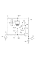
図3には、光電変換装置の画素100の等価回路が示されている。図5には、光電変換装置の画素100の断面構造が模式的に示されている。
FIG. 3 shows an equivalent circuit of the
図5において、半導体基板200の上には第1電極である上部電極101が配される。上部電極101と半導体基板200との間に第2電極である画素電極105が配される。上部電極101と画素電極105との間に第2ブロッキング層102が配される。第2ブロッキング層102の下部には光電変換層103が配される。光電変換層103の下部には、第1ブロッキング層104が配される。
In FIG. 5, an
ここで、光電変換層103は入射光に対応して正孔を蓄積するものとする。第2ブロッキング層102は、上部電極101から画素電極105への正孔の注入を抑制する。すなわち、第2ブロッキング層102は、光電変換層103が蓄積する電荷と同じ極性の電荷の、上部電極101から光電変換層103への注入を抑制する。
Here, it is assumed that the
以下では、本発明の実施形態について図面を用いて詳細に説明する。本発明は以下に説明される実施形態のみに限定されない。本発明の趣旨を超えない範囲で、以下に説明される実施形態の一部の構成が変更された変形例も、本発明の実施形態である。また、以下のいずれかの実施形態の一部の構成を、他の実施形態に追加した例、あるいは他の実施形態の一部の構成と置換した例も本発明の実施形態である。 Hereinafter, embodiments of the present invention will be described in detail with reference to the drawings. The present invention is not limited only to the embodiments described below. Modifications in which a part of the configuration of the embodiment described below is changed without departing from the gist of the present invention are also embodiments of the present invention. An example in which a part of the configuration of any of the following embodiments is added to another embodiment, or an example in which a part of the configuration of another embodiment is replaced is also an embodiment of the present invention.
(実施例1)
本実施例の光電変換装置について、図面を参照しながら説明する。
Example 1
The photoelectric conversion device of this example will be described with reference to the drawings.
(光電変換装置の構成)
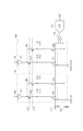
図1は、本実施例の光電変換装置の全体の回路構成と、上部電極101の配置レイアウトとを合わせて示した図である。
(Configuration of photoelectric conversion device)
FIG. 1 is a diagram showing the overall circuit configuration of the photoelectric conversion device of the present embodiment and the layout of the
図1は、複数行および複数列に渡って配された画素100の一部として、4行4列の行列状に配された16個の画素100が示されている。本実施例では4行4列の行列で説明するが、行数および列数はこれに限定されるものではない。1つの列に含まれる複数の画素100が、1つの出力線130に接続される。1つの出力線130に対して、1つの電流源150が接続されている。この電流源150は、画素100に電流を供給する。画素100は、出力線130に、画素信号を出力する。この画素信号は、入射光に基づく信号である光信号と、画素100のノイズ成分を主とするノイズ信号とを含む。
FIG. 1 shows 16
光電変換装置は、電圧制御部110と、行駆動回路201を有する。電圧制御部110は、行駆動回路201が供給する電圧Vsの生成に用いる基準電圧を供給する。行駆動回路201は、電極駆動電圧Vs、リセット信号pRES、駆動信号pSELを供給する。1つの行に含まれる複数の画素100は同一のリセット信号線、駆動信号線に接続される。リセット信号線は、リセット信号pRESを伝達する配線である。駆動信号線は、駆動信号pSELを伝達する配線である。なお、図1では、異なる行に供給される駆動信号を区別するために、(n)、(n+1)といったように行を表す符号を信号の末尾に付している。他の図面でも同様である。
The photoelectric conversion device includes a
図1では、上部電極101の平面構造を模式的に示している。1行の画素100に対して、1つの上部電極101が対応して設けられている。本実施例では、それぞれの行ごとに上部電極101が配される。行駆動回路201は電圧Vsを行単位で供給する。電圧Vsは第1電圧と、第1電圧とは電圧値の異なる第2電圧とを含む。行駆動回路201は上部電極101に、値の異なる複数の電圧を供給する電圧供給部である。なお、異なる行に供給される電圧Vsを区別するために、(n)、(n+1)などの行を表す符号を付している。
FIG. 1 schematically shows a planar structure of the
光電変換装置は、列回路140を有する。図1では、複数列の列回路140を、簡易的に1つのブロックとして示しているが、実際には1つの出力線130に対して、1つの列回路140が設けられた構成となっている。
The photoelectric conversion device includes a
列駆動回路202は、駆動信号CSELを複数の列回路140に供給する。列駆動回路202は、駆動信号CSELを列回路140ごとに順次アクティブレベルとする。これにより、列駆動回路202は、列回路140を列ごとに駆動する。なお、異なる列に供給される駆動信号を区別するために、(m)、(m+1)などの列を表す符号を付している。他の図面でも同様である。
The
列駆動回路202によって、複数の列回路140のそれぞれから、信号が出力アンプ部203に出力される。出力アンプ部203は、入力された信号を増幅した信号を、AD変換部204に出力する。AD変換部204は、入力された信号をデジタル信号に変換した信号を、光電変換装置の外部に信号DOUTとして出力する。
The
(列回路の構成)
図2は、m列目およびm+1列目の列回路140の等価回路を示した図である。図2の列回路140は、図1に示した列回路140のうちの2列に対応する。
(Configuration of column circuit)
FIG. 2 is a diagram showing an equivalent circuit of the
出力線130に出力された画素信号は、列アンプ301によって増幅される。列アンプ301の出力ノードは、S/Hスイッチ303を介して容量CTSに接続されている。また、列アンプ301の出力ノードは、S/Hスイッチ305を介して容量CTNに接続されている。S/Hスイッチ303およびS/Hスイッチ305は、それぞれ、不図示のタイミングジェネレータから出力される駆動信号pTSおよび駆動信号pTNによって制御される。このような構成により、画素100が出力するノイズ信号に基づく信号を容量CTNが保持する。また、ノイズ信号を成分の一部として含む光信号を容量CTSが保持する。
The pixel signal output to the
容量CTSは、水平転送スイッチ307を介して水平出力線311に接続されている。容量CTNは、水平転送スイッチ309を介して水平出力線313に接続されている。水平転送スイッチ307、309は、列駆動回路202からの駆動信号CSELによって制御される。
The capacitor CTS is connected to the
水平出力線311と水平出力線313のそれぞれは出力アンプ部203に接続されている。出力アンプ部203は、水平出力線311の信号と水平出力線313の信号との差分をAD変換部204に出力する。出力アンプ部203は、光信号とノイズ信号との差分を得る。これにより、光信号に含まれていたノイズ信号を、光信号から差し引いた信号を得ることができる。AD変換部204は、出力アンプ部203が出力する信号をデジタル信号に変換する。
Each of the
なお、この例では、列回路140から水平転送された信号をAD変換する構成としている。他の例として、各列の列回路140がAD変換部を備えるようにしてもよい。この場合、AD変換部は、メモリやカウンタなどの、画素信号に対応するデジタル信号を保持する保持部を有する。保持部には、ノイズ信号と光信号がそれぞれデジタル信号に変換されて保持される。
In this example, the signal horizontally transferred from the
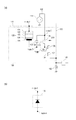
(画素の構成)
図3(a)は、光電変換装置の画素100の等価回路と、光電変換部120の模式図とを合わせて示した図である。図3(b)は、光電変換部120の等価回路を示した図である。
(Pixel configuration)
FIG. 3A is a diagram illustrating an equivalent circuit of the
図3(a)に示した画素100は、図1に示した画素100と対応する。
The
画素100は、光電変換部120、増幅トランジスタ(SF MOS)106、選択トランジスタ(SEL MOS)107、リセットトランジスタ(RES MOS)108、不純物拡散部であるFD部を含む。
The
光電変換部120は、上部電極101、光電変換層103、画素電極105を備える。さらに光電変換部120は、光電変換層103と画素電極105との間に第1ブロッキング層104を有する。また、光電変換部120は、光電変換層103と上部電極101との間に第2ブロッキング層102を有する。
The
上部電極101には、行駆動回路201からVs線131を介して電圧Vsが供給される。
A voltage Vs is supplied to the
第1ブロッキング層104は、半導体材料で形成されうる。半導体材料は、シリコン、ゲルマニウム、ガリウム砒素などの無機半導体材料、および、有機半導体材料の中から選択されうる。また、光電変換層103を形成する半導体材料と、第1ブロッキング層104を形成する半導体材料とが異なっていてもよい。あるいは、光電変換層103を形成する半導体材料のバンドギャップと第1ブロッキング層104を形成する半導体材料のバンドギャップとが異なっていてもよい。バンドギャップは、伝導帯(conduction band)の最低のエネルギー準位と、価電子帯(valence band)の最高のエネルギー準位との差である。なお、第1ブロッキング層104を形成する材料は半導体材料に限定されない。
The
また、光電変換層103と第1ブロッキング層104とを同じ半導体材料で形成するようにしてもよい。この場合には、光電変換層103と第1ブロッキング層104とで、半導体材料に添加する不純物の濃度を異ならせるようにすることによって、光電変換層103と第1ブロッキング層104とを形成することができる。
Further, the
図3(a)のノードBは、画素電極105と、容量素子109の一方のノードと、不純物拡散部であるFD部とに接続されている。容量素子109は容量値Cpを有する。
Node B in FIG. 3A is connected to the
図3(a)のノードCは、リセットトランジスタ108のドレインと、容量素子109の他方ノードとに接続される。さらにリセットトランジスタ108は、基準電圧制御部110に接続される。増幅トランジスタ106のゲートは、画素増幅部の入力ノードである。このような構成により、画素増幅部が光電変換部120からの信号を増幅した信号を、出力線130に出力する。
A node C in FIG. 3A is connected to the drain of the
増幅トランジスタ106のドレインは、電源電圧Vdd(例えば3.3V)が供給されたノードに接続される。増幅トランジスタ106のソースは、選択トランジスタ107を介して、出力線130に接続される。選択トランジスタ107がオンすることによって、電流源150から出力線130、選択トランジスタ107を介して増幅トランジスタ106に電流が供給される。これにより、増幅トランジスタ106と電流源150とによって、ソースフォロワ回路が構成される。このソースフォロワ回路を構成する増幅トランジスタ106は、光電変換部120からの信号に対応する信号を出力線130に出力する。画素100の増幅トランジスタ106が出力した信号は、列回路140に入力される。つまり、選択トランジスタ107は、増幅トランジスタ106と、出力線130との間の電気的経路の導通と非導通とを切り替えるトランジスタである。
The drain of the
図3(b)は光電変換部120の等価回路を示す。光電変換部120は、図3(a)のノードAに接続された第1端子、および、ノードBに接続された第2端子を有するフォトダイオードを形成する。
FIG. 3B shows an equivalent circuit of the
(光電変換部の構成)
上述した図3(a)、図3(b)の光電変換部120の具体的な構成について詳細に説明する。
(Configuration of photoelectric conversion unit)
A specific configuration of the
本実施例の第1ブロッキング層104と、光電変換層103と、第2ブロッキング層102は、ホモ接合を構成するようにすることができる。つまり、第1ブロッキング層104と、光電変換層103と、第2ブロッキング層102のそれぞれが、同じ半導体材料で形成されるようにすることができる。この「同じ半導体材料」とは、第1ブロッキング層104と、光電変換層103と、第2ブロッキング層102のそれぞれにおいて、最も多く含まれる元素が同じであることを指している。例えば、ケイ素に対して不純物を添加することによって形成された半導体によって第1ブロッキング層104と、光電変換層103と、第2ブロッキング層102のそれぞれが形成されたとする。この場合、第1ブロッキング層104と、光電変換層103と、第2ブロッキング層102のそれぞれが最も多く含む元素はケイ素である。したがって、第1ブロッキング層104と、光電変換層103と、第2ブロッキング層102のそれぞれが「同じ半導体材料」で形成されたと言える。
The
光電変換層103を構成する材料として、半導体材料、化合物半導体や有機半導体を用いることができる。半導体材料の例としては、真性の(イントリンシックな)アモルファスシリコン、低濃度のP型アモルファスシリコン、低濃度のN型アモルファスシリコンなどが挙げられる。化合物半導体の例としては、BN、GaAs、GaP、AlSb、GaAlAsPなどのIII−VI族化合物半導体や、CdSe、ZnS、HdTeなどのII−IV族化合物半導体が挙げられる。有機半導体の例としては、フラーレン、クマリン6(C6)、ローダミン6G(R6G)、キナクリドン、亜鉛フタロシアニン(ZnPc)等のフタロシアニン系材料、ナフタロシアニン系材料が挙げられる。
As a material constituting the
さらに、上述の半導体材料で構成された量子ドットを含む層を光電変換層103に用いることができる。非晶質シリコン膜、有機半導体膜、量子ドット膜は、薄膜の形成が容易である。ここで、量子ドットとは、20.0nm以下の粒径を有する粒子を示す。
Furthermore, a layer including quantum dots formed using the above-described semiconductor material can be used for the
また、イントリンシックな半導体は、キャリア密度が少ない。よって、イントリンシックな半導体を光電変換層103に用いることで、広い空乏層幅を実現することが可能である。これにより、高感度化、ノイズ低減を低減した光電変換層103を実現することができる。
Intrinsic semiconductors have a low carrier density. Therefore, by using an intrinsic semiconductor for the
上部電極101は、不図示のマイクロレンズ層および不図示のカラーフィルタ層を介して入射した光を光電変換層103に透過するような材料で形成される。例えば、上部電極101には、ITOのようにインジウムおよびスズを含む化合物、酸化物などの透明電極を用いることができる。透明電極を用いることにより、上部電極101を透過することによるによる入射光の光量低下を抑制できるため、光電変換部120の感度の低下を抑制することができる。他の上部電極101の例として、所定の量の光が透過する程度の薄さを有するポリシリコンや金属を、上部電極101として用いてもよい。金属は酸化物に比べて電気抵抗が低いため、金属を上部電極101の材料に用いた場合には、酸化物の上部電極101に対して、消費電力の低減と駆動の高速化が可能である。
The
第1ブロッキング層104と、光電変換層103と、第2ブロッキング層102のそれぞれが「同じ半導体材料」で形成される場合、それぞれが含む不純物濃度を互いに異ならせるようにする。例えば、第2ブロッキング層102はN型の半導体材料で形成され、光電変換層103はイントリンシックな半導体で形成され、第1ブロッキング層104がP型の半導体材料で形成される。つまり、光電変換層103の導電型(I型)と、ブロッキング部である第1ブロッキング層104の導電型(P型)とが異なる。さらに、第1ブロッキング層104の導電型(P型)と第2ブロッキング層102の導電型(N型)とが異なる。
When each of the
また、第1ブロッキング層104を、光電変換層103とは異なる材料で形成することができる。このような構成の場合、第1ブロッキング層104と光電変換層103との間にはヘテロ接合が形成される。第1ブロッキング層104と光電変換層103との材料の違いは、第1ブロッキング層104と光電変換層103との間にエネルギー障壁を生成する。したがって、このヘテロ接合により、信号電荷とは逆の極性の電荷の、光電変換層103から画素電極105への注入を抑制(ブロッキング)することができる。なお、ここで言う「異なる材料」とは、その層を形成する主たる元素が異なることを指している。
In addition, the
もしくは、光電変換層103とは異なる材料でブロッキング層を構成することができる。このような構成によればヘテロ接合が形成される。材料の違いによりバンドギャップが異なるため、電子および正孔のうち一方に対してのみポテンシャルバリアを形成することができる。
Alternatively, the blocking layer can be formed using a material different from that of the
第2ブロッキング層102と第1ブロッキング層104は、光電変換部120がダイオード特性を有するように構成される。つまり第2ブロッキング層102にN型の半導体を用いた場合、第1ブロッキング層にはP型の半導体を用いる。このとき信号電荷は正孔を利用する。
The
画素電極105は金属などの導電部材で構成される。画素電極105には、配線を構成する導電部材、あるいは、外部と接続するためのパッド電極を構成する導電部材と同じ材料が用いられる。このような構成によれば、画素電極105と、配線を構成する導電部材、あるいは、パッド電極とを同時に形成することができる。したがって、製造プロセスを簡略化することができる。
The
(画素の平面構造・断面構造の説明)
次に、本実施例の光電変換装置の平面構造、断面構造について説明する。
(Description of planar structure and cross-sectional structure of pixel)
Next, a planar structure and a cross-sectional structure of the photoelectric conversion device of this example will be described.
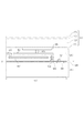
図4は、2行2列の行列状に配された4個の画素100の平面構造を模式的に示している。その他の画素も同様の平面構造を有している。ここでは画素電極105より上部に積層される光電変換部は省略している。
FIG. 4 schematically shows a planar structure of four
図5は、図4におけるX−Yの一点破線に沿った光電変換装置の画素100の断面構造を模式的に示している。なお、図1と同じ機能を有する部分には同じ符号を付してある。トランジスタについては対応するゲート電極に符号が付されている。ここで画素電極105の上部に積層される光電変換部も表示している。
FIG. 5 schematically shows a cross-sectional structure of the
以下図4、図5を用いて画素の構造について説明する。光電変換装置は半導体基板200を含む。本実施形態において半導体基板200はP型半導体からなる。半導体基板200に、画素トランジスタのソース領域およびドレイン領域を含めた、不図示のN+型不純物半導体領域(不純物拡散部)が配される。画素トランジスタとは、例えば、増幅トランジスタ106、選択トランジスタ107、リセットトランジスタ108である。半導体基板200の上に、画素トランジスタのゲート電極、および、配線を構成する導電部材を含む複数の配線層212が配される。画素電極部をゼロバイアス駆動するための容量素子109の一方のノードである第1ノード501、他方のノードである第2ノード502を示す。容量素子109は、第1ノード501、第2ノード502と、その間に配された層間絶縁層により構成される。
Hereinafter, the structure of the pixel will be described with reference to FIGS. The photoelectric conversion device includes a
図4において、電圧制御線132から分岐する配線により、リセットトランジスタ108のドレインと容量素子109の第2ノード502にリセット電圧Vresが供給される。具体的には、分岐点P1において、電圧制御線132から各画素の配線に分岐される。また、分岐点P2において、リセットトランジスタ108のドレインと容量素子109の第12ノード502に分岐される。このように、本実施例の光電変換装置は、1つの電圧制御線132から、各画素の領域内で分岐する構造とする。分岐点P2を設けることにより、リセットトランジスタ108と容量素子109とに電圧を供給する配線を共通化することができる。これにより、本実施例の光電変換装置は、1行複数列に配された複数の画素100に渡って配される電圧制御線132の本数を、減らすことができる。また、本実施例の光電変換装置は、電圧制御線132の本数を減らすことができるため、電圧制御部110が電圧制御線132に電圧を出力するバッファ回路を備える場合には、このバッファ回路の数も減らすことができる。
In FIG. 4, the reset voltage Vres is supplied to the drain of the
本実施例では、電源電圧Vddは電源線(Vdd線)135から各行の画素に供給されている。他の例として、上部電極101に供給される電源電圧Vsが電源電圧Vddを兼ねてもよい。これにより電源電圧Vddを供給する電源線135を省略することができる。これにより、電源電圧Vddを供給する配線の面積の分、画素領域の配線面積を縮小できる。
In this embodiment, the power supply voltage Vdd is supplied from the power supply line (Vdd line) 135 to the pixels in each row. As another example, the power supply voltage Vs supplied to the
(光電変換部の機能と電子シャッター動作の説明)
次に、本実施例における画素100の動作、ならびに、第1ブロッキング層104、光電変換層103、第2ブロッキング層102の機能について詳しく説明する。
(Explanation of photoelectric converter function and electronic shutter operation)
Next, the operation of the
図6は光電変換部120に入射光が全く入らない状態(暗時とする)における、I−V特性を示している。図6において、縦軸は上部電極101と画素電極105との間に流れる電流Id、横軸は光電変換部120に印加される電圧Vbを示す。この電圧Vbは、上部電極101と画素電極105との間の電圧差である。電圧Vfはフォトダイオードの順方向の立ち上がり電圧である。
FIG. 6 shows IV characteristics in a state where no incident light enters the photoelectric conversion unit 120 (when dark). In FIG. 6, the vertical axis represents the current Id flowing between the
光電変換部120が光電変換を行う場合(光電変換モード)の上部電極101と画素電極105の電圧の大小関係は、光電変換層103に逆バイアスが印加される関係となる。光電変換層103に光が入射すると、光電変換層103に電子と正孔が生じる。光電変換モードのバイアス条件では、光電変換層103に生じた正孔は画素電極105に移動し、電子は上部電極101に移動する。画素電極105は、この光電変換層103で生じた正孔を蓄積する。
When the
光電変換層103に順バイアスが印加され、かつ立ち上がり電圧Vfより高い範囲に電圧VbがあるAモードでは、上部電極101から光電変換層103に電子が注入される。
In the A mode in which a forward bias is applied to the
光電変換層103に順バイアスが印加され、かつ立ち上がり電圧Vfより低い範囲に電圧VbがあるBモードでは、光電変換部120は、後述する電子シャッター動作を行う状態となる。
In the B mode in which a forward bias is applied to the
図7(a)、図7(b)は、光電変換部120に印加される電圧のバイアス条件と、このバイアス条件における光電変換部120におけるエネルギーバンド構造とを模式的に示している。図7(a)は図6における光電変換モード(信号電荷を画素電極105が蓄積するモード)に対応する。図7(b)は図6におけるBモード(電子シャッターを行うモード)に対応する。図7(a)、図7(b)の縦軸は、電子、正孔に対するポテンシャルを示している。図7の下に行くほど、電圧は高くなる。
FIGS. 7A and 7B schematically show the bias condition of the voltage applied to the
図7(a)、図7(b)のそれぞれは、上部電極101、第2ブロッキング層102、光電変換層103、第1ブロッキング層104、画素電極105のエネルギーバンドを示している。図7(a)では、一例として、上部電極101がITO、画素電極105がTiNxで形成されている場合を示している。以下、他の図面に示しているエネルギーバンド図についても、特に断りのない限り、上部電極101および画素電極105の材料は図7(a)と同じである。
7A and 7B show energy bands of the
図7(a)、図7(b)に示した電圧Ef1は上部電極101のフェルミ準位であり、電圧Ef2は画素電極105のフェルミ順位である。第2ブロッキング層102、光電変換層103、第1ブロッキング層104に関しては、伝導帯と価電子帯との間のバンドギャップが示されている。
The voltage Ef1 shown in FIGS. 7A and 7B is the Fermi level of the
図7(a)は、図6における光電変換モードに対応する。光電変換部120が光電変換を行って生成した電荷のうちの信号電荷である電子が、画素電極105に蓄積される状態のポテンシャルを示す。光電変換によって生じた正孔を黒丸で示しており、電子を白丸で示している。光電変換部120が光電変換モードとなるように、上部電極101に供給される電圧Vsが、第1電圧である電圧Vs1(例えばVddと同じ3.3V)に設定される。逆バイアス状態にある光電変換層103は空乏化している。
FIG. 7A corresponds to the photoelectric conversion mode in FIG. The potential of a state in which electrons, which are signal charges out of the charges generated by the
光電変換層103で生成した電荷のうちの電子は、画素電極105に移動する。光電変換モードの間、画素電極105には、光電変換層103が生成した電子が蓄積されていく。この画素電極105に蓄積された信号電荷量に応じて、ノードBの電圧が低下する。ノードBの電圧の低下により、光電変換層103のバンド構造は、フラットバンド状態に向かって変化する。
Electrons out of the charges generated in the
なお、光電変換部120は第2ブロッキング層102を備える。これにより、上部電極101から光電変換層103への正孔の注入が抑制される。このため、上部電極101から光電変換層103に正孔が注入されることによって生じる暗電流の発生を抑えることができる。つまり、第2ブロッキング層102は、信号電荷と同じ極性の電荷である正孔の、上部電極101から光電変換層103への注入を抑制する第2ブロッキング部である。
Note that the
光電変換層103で発生した電子は、上部電極101に向かって移動することによって、光電変換部120の外部に排出される。
Electrons generated in the
光電変換部120は第1ブロッキング層104を備える。これにより、画素電極105から光電変換層103への電子の注入を抑制することができる。これにより、光電変換層103における、正孔と電子の再結合の発生を抑制することができる。よって、画素電極105から光電変換層103への電子の注入によって生じる、感度の低下が抑制される。つまり、第1ブロッキング層104は、信号電荷である正孔を光電変換層103から画素電極105に注入させ、信号電荷とは反対の極性の電荷である電子の光電変換層103から画素電極105への注入を抑制するブロッキング部である。なお、第1電極は上部電極101であり、第2電極は画素電極105である。
The
図7(b)は、図6のBモードに対応した光電変換部120のポテンシャルを示す。図6に示したBモードでは、電子シャッター動作を実現する。光電変換の開始と、光電変換モードからBモードへの移行の動作のそれぞれを、図1に示した全ての画素100が同時に行うことによって、グローバル電子シャッターを実現することができる。光電変換部120がBモードとなるように、上部電極101に供給される電圧Vsが、第2電圧である電圧Vs2(例えば0V)に設定される。信号電荷が正孔であるので電圧Vs1と電圧Vs2の電圧には、Vs2<Vs1の関係がある。
FIG. 7B shows the potential of the
Bモードでは、光電変換層103はフラットバンド状態に近い状態にある。つまり、上部電極101からの正孔の注入はほとんど生じない。また、光電変換層103に印加されるバイアスが小さいため、光電変換によって生じた正孔の光電変換層103の外部への移動は、ほとんど生じない。光電変換層103で生成した電子の光電変換層103の外部への移動もまた、ほとんど生じない。したがって、画素電極105に蓄積されている正孔、電子の量の変動がほとんど生じない。この状態は、画素電極105に蓄積されている正孔が保持されている状態と、みなすことができる。したがって、本実施例の画素100は、光電変換部120が光電変換モードからBモードに移行することによって、光電変換部120の電荷蓄積期間が終了する。
In the B mode, the
(グローバルシャッター動作の説明)
図8は、本実施形態の光電変換装置に用いられるグローバルシャッター動作における駆動信号のタイミングチャートを示している。図8には、簡単のためn行目とn+1行目の2行分の信号読み出し動作に対応した駆動信号が示されている。
(Explanation of global shutter operation)
FIG. 8 shows a timing chart of drive signals in the global shutter operation used in the photoelectric conversion device of this embodiment. For the sake of simplicity, FIG. 8 shows drive signals corresponding to the signal read operations for the nth and n + 1th rows.
時刻t1から時刻t2の間、光電変換部120を、図7(a)に示される光電変換モードになるように、全行の第1の電極101に共通電極駆動電圧Vs(n)にVs1(例えば3.3V)を供給する。この間全画素一括で光電変換が行われ、光信号電荷(正孔)が画素電極105に蓄積される(一括露光)。同時にリセット電圧Vres(n)がローレベルV2(例えば0V)になる。このときバイアス制御容量Cp109を介してノードB、FD部の電位が振り下げられる。この動作によりノードB、FD部はゼロバイアス駆動状態に設定され、増幅トランジスタ106と電流源150で構成される画素ソースフォロワ回路のダイナミックレンジから外れる。
Between time t1 and time t2, the
時刻t2において、光電変換部120が、図7(b)に示されるBモードになるように、全行の上部電極101に電圧Vs(n)としてVs2(例えば1.5V)を供給する。この間、全ての画素の光電変換部の感度が、一括して実質的にゼロとなる。また同時に行選択信号pSEL(n)がハイレベルになり、n行目の画素100の選択トランジスタ107がオンする。これにより、n行目の画素100の増幅トランジスタ106が信号を出力する。またリセット電圧Vres(n)がハイレベルのVr2(例えば1.5V)になる。このとき、容量素子109を介してノードB、FD部の電位が振り上げられる。後述するように、この動作によりノードB、FD部はゼロバイアス駆動状態から、増幅トランジスタ106と電流源150で構成される画素ソースフォロワ回路のダイナミックレンジに入る読み出し状態に設定される。
At time t2, the
駆動信号pTS(n)が、時刻t3においてハイレベルになり、時刻t4においてローレベルになる。これにより、ノードBに蓄積された光信号と増幅トランジスタ106の閾値ばらつきとを含む信号Sが、列回路140の容量CTSに保持される。
The drive signal pTS (n) becomes high level at time t3 and becomes low level at time t4. As a result, the signal S including the optical signal stored in the node B and the threshold variation of the
時刻t5において、リセット信号pRES(n)がハイレベルになり、時刻t6において、駆動信号pRES(n)がローレベルになる。この間に、リセット電圧Vres(n)はVr2に維持されているので、ノードBとFD部の信号電荷がリセットされ、リセット電圧Vres(n)の1.5Vに設定される。 At time t5, the reset signal pRES (n) becomes high level, and at time t6, the drive signal pRES (n) becomes low level. During this time, since the reset voltage Vres (n) is maintained at Vr2, the signal charges of the node B and the FD portion are reset and set to 1.5V of the reset voltage Vres (n).
その後、時刻t7において駆動信号pTN(n)がハイレベルになり、時刻t8においてローレベルになる。これにより、増幅トランジスタ106の閾値ばらつきを含む信号Nが、列回路140の容量CTNに保持される。
Thereafter, the drive signal pTN (n) becomes high level at time t7 and becomes low level at time t8. As a result, the signal N including the threshold variation of the
時刻t9において、行選択信号pSEL(n)がローレベルになり、n行目の画素100から列回路140への信号の読み出しが終了する。
At time t9, the row selection signal pSEL (n) becomes low level, and reading of signals from the
列回路140に読み出されたノイズ信号Nと光信号Sは、駆動信号CSELに基づいて、列ごとに出力部170に出力される。出力部170は信号Sと信号Nとの差分をアナログ−デジタル変換部(ADC)204に出力する。
The noise signal N and the optical signal S read out to the
時刻t10おいて、行選択信号pSEL(n+1)がハイレベルになり、n+1行目の画素100の選択トランジスタ107がオンする。以降、n+1行目の画素100からの信号の読み出しが行われる。この動作は時刻t1から時刻t9と同様なので、説明を省略する。
At time t10, the row selection signal pSEL (n + 1) becomes high level, and the
各行の信号読み出し中、全行の上部電極101には電圧VsとしてVs2(1.5V)が印加されている。つまり、全ての画素はBモードに設定されている。
During signal reading of each row, Vs2 (1.5 V) is applied as the voltage Vs to the
以下同様に最後の行まで信号を読み出したのち、不図示のタイミングで全行のリセット電圧Vres(n)が一括でVr2(1.5V)に設定され、リセット信号pRESがハイレベルになり、所定の時間後ローレベルになる。これにより全画素のノードBがVr2(1.5V)にリセットされる(一括リセット)。読み出し期間中リセット電圧Vres(n)をVr2(1.5V)に維持してもよい。 Similarly, after reading out signals to the last row, reset voltages Vres (n) of all rows are collectively set to Vr2 (1.5V) at a timing (not shown), and the reset signal pRES becomes high level. After that time, it goes low. Thereby, the node B of all the pixels is reset to Vr2 (1.5 V) (collective reset). The reset voltage Vres (n) may be maintained at Vr2 (1.5 V) during the reading period.
再び時刻t1のタイミングに戻り、光電変換部120を、図7(a)に示される光電変換モードになるように、全行の上部電極101に電圧VsとしてVs1(3.3V)を印加する。この電圧Vs1が上部電極101に印加されている間、全画素一括で光電変換モードに設定される(一括露光)。同時にリセット電圧Vres(n)がローレベルV2(例えば0V)になる。このとき容量素子109を介してノードB、FD部の電位が振り下げられる。この動作によりノードB、FD部はゼロバイアス駆動状態に設定され、増幅トランジスタ106と電流源150で構成される画素ソースフォロワ回路のダイナミックレンジから外れる。このようにして、次のフレームの信号蓄積を行う。
Returning again to the timing of time t1, Vs1 (3.3V) is applied as the voltage Vs to the
(第1ブロッキング層104を備えることによる効果)
図9(a)〜図9(e)のそれぞれを用いて、本実施例の効果を説明する。図9(b)、図9(c)は参考例であって、光電変換部120が第1ブロッキング層104を有しない例を示している。図9(d)、図9(e)は、これまでに述べてきた、光電変換部120が第1ブロッキング層104を有する例を示している。ただしここでは信号電荷として電子を利用する(電子蓄積型)場合で説明する。正孔を利用する場合も同様の効果がある。
(Effect by providing the 1st blocking layer 104)
The effect of the present embodiment will be described with reference to FIGS. 9A to 9E. FIG. 9B and FIG. 9C are reference examples and show an example in which the
図9(a)は、光電変換装置に入射した像を示している。P1の位置にある画素100の光信号はダークレベルに近いレベルであり、P2の位置にある画素100の光信号は飽和レベルに近いレベルである。このように撮像シーンによっては、1枚の像の中に、ダークレベルに近い画素P1、飽和レベルに近い画素P2が存在する。
FIG. 9A shows an image incident on the photoelectric conversion device. The optical signal of the
参考例である図9(b)、図9(c)を説明する。図9(b)は画素P1の光電変換部120のバンド構造を示している。図9(c)は画素P2の光電変換部120のばんどこうぞうを示している。図9(b)、図9(c)のそれぞれにおいて示した実線は、光電変換領域におけるバンド構造を示している。図9(b)、図9(c)のそれぞれにおいて示した点線は、Bモードにおけるバンド構造を示している。
Reference examples shown in FIGS. 9B and 9C will be described. FIG. 9B shows a band structure of the
図9(b)の画素P1の光電変換部120では、光電変換モードにおいて、実線で示したように、光信号による電子が画素電極105にほとんど蓄積されていない。よって、光電変換モードにおける、画素P1の光電変換部120のバンド構造は、光電変換部120のリセット時の逆バイアス状態に近いポテンシャルのままとなっている。
In the
図9(c)の画素P2の光電変換部120では、光電変換モードにおいて、実線で示したように、光信号による電子が画素電極105に蓄積され、ノードBの電圧が低下している。よって、光電変換モードにおける、画素P2の光電変換部120のバンド構造は、フラットバンド状態に近い状態になっている。
In the
ここで、ダークレベルに近い光信号を出力する画素P1が、Bモードにおいてフラットバンドとなるように電圧Vs2の電圧を設定したとする。よって、図9(b)において点線で示したように、画素P1の光電変換部120は、Bモードにおいて、フラットバンド状態に近い状態になっている。
Here, it is assumed that the voltage Vs2 is set so that the pixel P1 that outputs an optical signal close to the dark level has a flat band in the B mode. Therefore, as indicated by a dotted line in FIG. 9B, the
図9(c)の画素P2の光電変換部120では、Bモードにおいて、点線で示したように、上部電極101の電圧が、画素電極105の電圧よりも相対的に高くなる。よって、光電変換部120がBモードにある間、光電変換層103で発生する正孔が画素電極105に移動しやすくなる。
In the
この光電変換層103中で発生する正孔が画素電極105に移動することによって、画素電極105に蓄積されていた電子が、消失することとなる。よって、画素P2の光信号が、本来出力すべき信号レベルから低下した信号レベルとなる。これにより、光電変換装置が出力した信号を用いて生成した画像において、高輝度の部分の輝度が低下する。つまり、画素電極105に蓄積されていた電子が消失せずに生成されたと仮定される画像に対して、コントラストが低下した画像が生成されることとなる。
As holes generated in the
本実施例の光電変換部120は、第1ブロッキング層104を有する。
The
図9(d)は、本実施例の光電変換部120を備える画素P1のバンド構造を示している。図9(d)では、図9(b)と同じく、画素P1の光電変換部120は、Bモードにおいて、フラットバンド状態に近い状態になっている。
FIG. 9D shows a band structure of the pixel P1 including the
図9(e)において、画素P2の光電変換部120がBモードにある場合のバンド構造を点線で示している。光電変換層103で発生する正孔の光電変換層103から画素電極105への移動は、第1ブロッキング層104によって、抑制されている。
In FIG. 9E, the band structure when the
このように、光電変換部120が第1ブロッキング層104を有することによって、光電変換層103中で発生する正孔の画素電極105への移動が抑制されている。よって、図9(c)では生じていた、画素電極105に蓄積されていた電子の消失もまた抑制される。よって、図9(c)では生じていた、画素P2の光信号の信号レベルの低下もまた、抑制される。これにより、図9(c)では生じていた、光電変換装置が出力した信号を用いて生成した画像における、高輝度の部分の輝度の低下もまた、抑制される。したがって、本実施例の光電変換装置は、従来の電子シャッター動作によって生じていた、画像のコントラストの低下を抑制することができる効果を有する。
As described above, since the
なお、本実施例において、信号電荷が正孔であるとして説明したが、電子を信号電荷としても同じ効果が得られる。 In the present embodiment, the signal charge is described as being a hole, but the same effect can be obtained by using an electron as the signal charge.
(容量素子109と電圧制御部110の説明)
以下図面を用いて本発明における容量素子109と電圧制御部110の機能について詳述する。
(Description of
Hereinafter, functions of the
図10は画素電極105が接続されるFD部の暗時のIV特性を示す模式図である。FD部などの不純物拡散部と半導体基板は、ダイオードを構成することがある。この場合について、図10は、縦軸をダイオードに流れる電流、横軸をダイオードにかかるバイアス電圧Vbとして示した図である。
FIG. 10 is a schematic diagram showing IV characteristics in the dark of the FD portion to which the
図10において、点P1は逆バイアス状態を示している。また点P2はゼロバイアス状態を示している。また、点P3は順バイアス状態を示している。一般に不純物拡散部は半導体基板と電気的に分離するために点P1の逆バイアス状態に設定される。しかしながら不純物拡散部と半導体基板の間には欠陥が生じやすく、その欠陥を介してリーク電流が流れる。リーク電流は不純物拡散部と半導体基板の間に印加された逆バイアス電圧に依存するので、逆バイアス電圧が強まるにつれて、リーク電流が多くなる。図10では、電流Iについて、リーク電流による成分も含めて示している。リーク電流は光電変換時(信号蓄積時)の暗電流となり、S/Nを劣化させるので好ましくない。 In FIG. 10, a point P1 indicates a reverse bias state. Point P2 indicates a zero bias state. Point P3 represents a forward bias state. In general, the impurity diffusion portion is set to a reverse bias state at point P1 in order to be electrically separated from the semiconductor substrate. However, a defect is likely to occur between the impurity diffusion portion and the semiconductor substrate, and a leak current flows through the defect. Since the leakage current depends on the reverse bias voltage applied between the impurity diffusion portion and the semiconductor substrate, the leakage current increases as the reverse bias voltage increases. In FIG. 10, the current I is shown including the component due to the leakage current. The leak current is not preferable because it becomes a dark current during photoelectric conversion (signal accumulation) and degrades S / N.
このリーク電流は、不純物拡散部の電圧をリセットした直後の期間である。この期間は、画素電極105が信号電荷の蓄積を行っている期間でもある。このリーク電流の影響を抑制するためには、不純物拡散部と半導体基板との間のバイアス電圧Vbを、0Vである点P2に設定するのが好ましい。つまり、不純物拡散部であるFD部に与えられる第1電圧と、FD部に接する半導体領域に与えられる所定の電圧とが略等しい状態とする。これをゼロバイアスリセットあるいはゼロバイアス駆動と言う。
This leakage current is a period immediately after resetting the voltage of the impurity diffusion portion. This period is also a period during which the
図11は増幅トランジスタ106および電流源150により構成される画素ソースフォロワ回路の入力電圧(FD部の電圧)Vfdと出力電圧Voutの関係を示す模式図である。Vminは画素ソースフォロワ回路がリニアリティを確保できるダイナミックレンジの最小値、Vmaxはダイナミックレンジの最大値を示す。P型半導体基板の電圧はGND(0V)に設定されている。Vminは1.5Vとし、Vmaxは2.5Vとする。
FIG. 11 is a schematic diagram showing the relationship between the input voltage (voltage of the FD section) Vfd and the output voltage Vout of a pixel source follower circuit constituted by the
本実施例では、正孔を信号電荷としている。画素電極105、FD部のリセット電圧は、画素ソースフォロワ回路のリニアリティを確保するために、Vmin以上の値にする。そこでリセット電圧を1.5Vとして、画素電極105、FD部をリセットする。画素電極105に集められた正孔は、FD部に蓄積される。したがって、FD部の電圧は時間の経過とともに上昇する。
In this embodiment, holes are used as signal charges. The reset voltage of the
FD部は、N型の不純物拡散部を有する。この不純物拡散部は、画素電極105とのコンタクト部を兼ねる。よって、FD部の不純物拡散部はN+型の半導体領域として表される。
The FD portion has an N-type impurity diffusion portion. This impurity diffusion portion also serves as a contact portion with the
画素電極105、FD部のリセットが解除された後のN+型の不純物拡散部の電圧は1.5Vである。また、P型半導体基板の電圧は0Vである。よって、1.5Vの逆バイアス状態となるため、リーク電流が多く発生することとなる。
The voltage of the N + type impurity diffusion portion after the reset of the
一方、ゼロバイアスリセットとして、0V近傍にリセット電圧を設定すると、画素電極105、FD部のリセットが解除された後のN+型の不純物拡散部の電圧は0V近傍の値となる。したがって、図11に示した、画素ソースフォロワ回路のダイナミックレンジの下限であるVminの値を下回ることとなる。よって、画素ソースフォロワ回路からの信号の精度の高い読み出しが行えない。
On the other hand, when a reset voltage is set in the vicinity of 0V as the zero bias reset, the voltage of the N + type impurity diffusion portion after the reset of the
そこで本発明では、リセット電圧は、画素ソースフォロワ回路のダイナミックレンジに収まる値(本実施例では1.5V)に設定する。また、信号蓄積中は、容量素子109に供給する電圧を、電圧制御部110が変化させることにより、画素電極105、FD部の電圧を振り下げる。これによって、図11に示した電圧Vbを、0V付近にシフトさせる。そして、画素ソースフォロワ回路が信号を出力する期間には、画素電極105、FD部の電圧を振り上げる。これにより、FD部の電圧を、画素ソースフォロワ回路のダイナミックレンジに収まるようにすることができる。これにより、画素ソースフォロワ回路が、FD部が蓄積した正孔の量に対応する信号を精度よく出力することができる。
Therefore, in the present invention, the reset voltage is set to a value (1.5 V in this embodiment) that falls within the dynamic range of the pixel source follower circuit. Further, during signal accumulation, the voltage supplied to the
このように、本実施例では、容量素子109の第2ノード502の電圧を、リセット時(1.5V)、信号蓄積時(0V)、読み出し時(1.5V)で変化させる。これにより、不純物拡散部と半導体基板との間で生じるリーク電流を低減しつつ、画素ソースフォロワ回路が精度よく信号を出力することができる。
Thus, in this embodiment, the voltage of the
容量素子109と電圧制御部110によるノードBの電圧の制御量(振り下げ幅、振り上げ幅)は、ノードCの電圧の変化量dVresに対して、容量素子109の容量値CpとノードBが有する容量の容量値C2との比に応じて決まる。ノードBの電圧の変化量dVBは、dVB=dVref×Cp/(Cp+C2)と表される。ノードBが有する容量の容量値には、光電変換部120が有する容量の容量値、ノードB周辺の他の寄生容量の容量値を含む。本実施例においては、ノードBが有する容量の容量値は、光電変換部120が有する容量の容量値が支配的である。容量素子109の容量値Cpを適宜設計することにより、ノードBの電圧の変化量dVBを制御することができる。
The amount of control of the voltage at node B (the swing-down width and the swing-up width) by the
本実施例では信号電荷が正孔で画素トランジスタがNMOSトランジスタの場合で説明した。他の例として、信号電荷が電子で、画素トランジスタがPMOSトランジスタの構成であっても同じ効果を得ることができる。 In this embodiment, the signal charge is a hole and the pixel transistor is an NMOS transistor. As another example, the same effect can be obtained even when the signal charge is an electron and the pixel transistor is a PMOS transistor.
(実施例2)
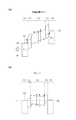
本実施例について、実施例1と異なる点を中心に説明する。
(Example 2)
The present embodiment will be described focusing on differences from the first embodiment.
実施例1の光電変換装置は、グローバルシャッター動作を行っていた。本実施例では、ローリングシャッターを行う点で、実施例1と異なる。 The photoelectric conversion device of Example 1 performed a global shutter operation. This embodiment is different from the first embodiment in that a rolling shutter is performed.
本実施例の光電変換装置の構成は、実施例1と同じとすることができる。 The configuration of the photoelectric conversion device of this embodiment can be the same as that of the first embodiment.
図12は、本実施例の光電変換装置の動作を示したタイミング図である。図12には、n行目の読み出し動作に対応した駆動信号が示されている。一方、図13には、n行目とn+1行目の2行分の信号の読み出し動作に対応した駆動信号を示している。 FIG. 12 is a timing chart showing the operation of the photoelectric conversion device of this example. FIG. 12 shows drive signals corresponding to the read operation of the nth row. On the other hand, FIG. 13 shows drive signals corresponding to the signal read operation for the two rows of the n-th row and the (n + 1) -th row.
行選択信号pSELは選択トランジスタ107のゲートに供給される。リセット電圧Vresはリセットトランジスタ108のドレインと容量素子109の一方のノードに供給される。リセット信号pRESはリセットトランジスタ108のゲートに供給される。駆動信号pTSはS/Hスイッチ303に供給される。駆動信号pTNはS/Hスイッチ305に供給される。駆動信号CSELは列回路140に供給される。
The row selection signal pSEL is supplied to the gate of the
行選択信号pSEL、リセット信号pRES、駆動信号pTS、駆動信号pTNがハイレベルの時に、対応するトランジスタまたはスイッチがオンする。行選択信号pSEL、リセット信号pRES、駆動信号pTS、駆動信号pTNがローレベルの時に、対応するトランジスタまたはスイッチがオフする。ここで不図示の電圧Vs(n)は、光電変換部120のノードAに供給されている。ローリングシャッター動作では、電圧Vs(n)は、光電変換部120が常に弱バイアス状態で光電変換モードとなるように、固定値(電源電圧Vddと同じ3.3V)に設定される。
When the row selection signal pSEL, the reset signal pRES, the drive signal pTS, and the drive signal pTN are at a high level, the corresponding transistor or switch is turned on. When the row selection signal pSEL, the reset signal pRES, the drive signal pTS, and the drive signal pTN are at a low level, the corresponding transistor or switch is turned off. Here, the voltage Vs (n) (not shown) is supplied to the node A of the
時刻t1より前の期間は、n行目の画素100の光電変換部120、および、n+1行目の画素100の光電変換部120の画素電極105が信号電荷を蓄積している状態である。また、リセット電圧Vres(n)はローレベルVr1(例えば0V)に設定されている。これにより、FD部はゼロバイアスリセットをされた後、ゼロバイアス駆動状態となっている。
In the period before time t1, the
時刻t1において、行選択信号pSEL(n)がハイレベルになり、n行目の画素100の選択トランジスタ107がオンする。これにより、n行目の画素100の増幅トランジスタ106が信号を出力する。
At time t1, the row selection signal pSEL (n) becomes high level, and the
時刻t2において、リセット電圧Vres(n)がハイレベルVr2(例えば1.5V)になる。このとき、容量素子109を介してノードBおよび、FD部の電圧が振り上げられる。これにより、ノードB、FD部はゼロバイアス駆動状態から、増幅トランジスタ106と電流源150で構成される画素ソースフォロワ回路のダイナミックレンジに入る読み出し状態に設定される。
At time t2, the reset voltage Vres (n) becomes the high level Vr2 (for example, 1.5V). At this time, the voltage of the node B and the FD portion is increased through the
時刻t3において、駆動信号pTS(n)がハイレベルになり、時刻t4においてローレベルになる。この間に、ノードBに蓄積された光信号と増幅トランジスタ106の閾値ばらつきとを含む信号Sが、列回路140の容量CTSに保持される。
At time t3, the drive signal pTS (n) becomes high level, and at time t4, it becomes low level. During this time, the signal S including the optical signal accumulated at the node B and the threshold variation of the
時刻t5において、リセット信号pRES(n)がハイレベルになり、時刻t6においてローレベルになる。この間に、リセット電圧Vres(n)はVr2である1.5Vに維持されているので、ノードBとFD部の信号電荷がこの1.5Vの電圧を用いてリセットされる。リセット電圧Vres(n)の1.5Vに設定されたあと光電変換モードになる。電圧Vs(n)は3.3Vであり、画素電極105の電圧は1.5Vなので、光電変換部120は逆バイアス状態となる。
At time t5, the reset signal pRES (n) becomes high level, and at time t6, it becomes low level. During this time, the reset voltage Vres (n) is maintained at 1.5 V which is Vr2, so that the signal charges at the node B and the FD portion are reset using the voltage of 1.5 V. After the reset voltage Vres (n) is set to 1.5 V, the photoelectric conversion mode is entered. Since the voltage Vs (n) is 3.3V and the voltage of the
その後、時刻t7において駆動信号pTN(n)がハイレベルになり、時刻t8においてローレベルになる。この間に、増幅トランジスタ106の閾値ばらつきを含む信号Nが、列回路140の容量CTNに保持される。光電変換部120が光電変換モードになった状態で光が入射していると、光により信号電荷が生成されるので、時刻t7と時刻t8の間隔は狭い方がよい。本実施形態では電圧Vs(n)は固定とした。他の例として、信号読み出し期間のHBLNK(n)中は、電圧Vs(n)をVs2に設定して、光電変換膜を不感状態とする。この不感状態の期間に、列回路140の容量CTNが信号Nを保持するようにしてもよい。
Thereafter, the drive signal pTN (n) becomes high level at time t7 and becomes low level at time t8. During this time, the signal N including the threshold variation of the
この後、n行目の画素100は、次のフレームの信号電荷の蓄積を開始する。信号電荷の蓄積中の、光電変換部120のエネルギーバンドの状態が、図7(a)に示されている。
Thereafter, the
時刻t9において、リセット電圧Vres(n)がローレベルV2(例えば0V)になる。このとき容量素子109を介してノードB、FD部の電圧が振り下げられる。この動作によりノードB、FD部はゼロバイアス駆動状態に設定される。これにより、本実施例の光電変換装置もまた、実施例1と同じく、FD部の不純物領域と半導体基板200と間で生じる暗電流を抑制した状態で、信号蓄積を行うことができる。
At time t9, the reset voltage Vres (n) becomes the low level V2 (for example, 0V). At this time, the voltages at the nodes B and FD are lowered through the
時刻t10において、行選択信号pSEL(n)がローレベルになり、n行目の画素100から列回路140への信号の読み出しが終了する。
At time t10, the row selection signal pSEL (n) becomes a low level, and reading of signals from the
列回路140に読み出されたノイズ信号Nと光信号Sは、駆動信号CSELに基づいて、列ごとに出力部170に出力される。出力部170は信号Sと信号Nとの差分をアナログ−デジタル変換部180に出力する。
The noise signal N and the optical signal S read out to the
以降図13に示すように、n+1行目の画素100からの信号の読み出しが行われる。この動作は時刻t1から時刻t8と同様なので、説明を省略する。
Thereafter, as shown in FIG. 13, signals are read from the
このように、本実施例においても、実施例1と同じく、回路面積を低減しながら、ノイズの少ない信号読み出しを行うことができる。 As described above, in this embodiment, as in the first embodiment, signal reading with less noise can be performed while reducing the circuit area.
(実施例3)
本実施例の光電変換装置について、実施例2と異なる点を中心に説明する。
(Example 3)
The photoelectric conversion device of this embodiment will be described focusing on differences from the second embodiment.
実施例1と同じ画素構成を備えていた実施例2の光電変換装置の画素100は、選択トランジスタ107を備えていた。本実施例は、画素100が選択トランジスタ107を有しない構成である。本実施例では、実施例2の画素100の選択トランジスタ107が行っていた、画素行の選択と非選択の切り替えを、電圧制御部110が出力する電圧を変更してFD部に与えることによって行う。
The
図14は、本実施例の光電変換装置が備える画素100の回路図である。本実施例の画素100は、上述した通り、選択トランジスタ107を有しない構成である。その他の構成については、実施例2の画素100の構成と同じである。
FIG. 14 is a circuit diagram of the
本実施例では、電圧制御部110がリセットトランジスタ108を介してFD部の電圧(FD電圧)を制御することで、行選択を行うことを特徴とする。これにより実施例1に対して選択トランジスタを省略できる。これにより、画素100の回路面積を低減できる。また、pSEL制御線を省略することができることから、画素領域の配線面積もまた低減できる。
This embodiment is characterized in that the
図15は、本実施例の光電変換装置に用いられるローリングシャッター動作における駆動信号のタイミングチャートを示している。以下、実施例2と異なる部分を中心にした説明を行う。 FIG. 15 shows a timing chart of drive signals in the rolling shutter operation used in the photoelectric conversion device of this embodiment. Hereinafter, the description will be focused on the parts different from the second embodiment.
時刻t1において、リセット電圧Vres(n)がハイレベルVr2(例えば1.5V)になる。このとき容量素子109を介してノードB、FD部の電圧が振り上げられる。図11で説明したように、この動作によりノードB、FD部はゼロバイアス駆動状態から、増幅トランジスタ106と電流源150で構成される画素ソースフォロワ回路のダイナミックレンジに入る読み出し状態に設定される。このときn行目の画素ソースフォロワ回路は動作状態となる。その他の行の画素ソースフォロワ回路は日動作状態となっている。つまりリセット電圧Vres(n)をハイレベルVr2に設定することで、n行目を選択する選択動作を行っている。
At time t1, the reset voltage Vres (n) becomes the high level Vr2 (for example, 1.5V). At this time, the voltages at the nodes B and FD are increased through the
時刻t2において、駆動信号pTS(n)がハイレベルになり、時刻t3においてローレベルになる。この間に、ノードBに蓄積された光信号と増幅トランジスタ106の閾値ばらつきとを含む信号Sが、列回路140の容量CTSに保持される。
At time t2, the drive signal pTS (n) becomes high level, and at time t3, it becomes low level. During this time, the signal S including the optical signal accumulated at the node B and the threshold variation of the
時刻t4において、リセット信号pRES(n)がハイレベルになり、時刻t5においてローレベルになる。この間に、リセット電圧Vres(n)はVr2に維持されているので、ノードBとFD部の信号電荷がリセットされ、リセット電圧Vres(n)の1.5Vに設定されたあと光電変換モードになる。電圧Vs(n)は3.3Vであり、画素電極105の電圧は1.5Vなので、光電変換部120は逆バイアス状態となる。
At time t4, the reset signal pRES (n) becomes high level and at time t5 becomes low level. During this time, since the reset voltage Vres (n) is maintained at Vr2, the signal charges at the node B and the FD portion are reset, and after the reset voltage Vres (n) is set to 1.5 V, the photoelectric conversion mode is set. . Since the voltage Vs (n) is 3.3V and the voltage of the
その後、時刻t6において駆動信号pTN(n)がハイレベルになり、時刻t7においてローレベルになる。この間に、増幅トランジスタ106の閾値ばらつきを含む信号Nが、列回路140の容量CTNに保持される。
Thereafter, the drive signal pTN (n) becomes high level at time t6 and becomes low level at time t7. During this time, the signal N including the threshold variation of the
時刻t8において、リセット電圧Vres(n)がローレベルVr1(例えば0V)になる。このとき、容量素子109を介してノードB、FD部の電圧が振り下げられる。この動作によりノードB、FD部はゼロバイアス駆動状態に設定される。よって、増幅トランジスタ106と電流源150で構成される画素ソースフォロワ回路のダイナミックレンジから外れる。これによりn行目の画素ソースフォロワ回路は非動作状態となり、非選択動作を実現することができる。
At time t8, the reset voltage Vres (n) becomes the low level Vr1 (for example, 0V). At this time, the voltage of the node B and the FD portion is lowered through the
電圧制御部110は、リセット電圧Vres(n)の電圧をVr1とVr2とに切り替える動作を行う。この動作により、選択トランジスタ107の働きを代用できる。これにより、選択トランジスタ107、pSEL信号線を省略することができる。これにより、上述したように、画素100の回路面積と、画素領域の配線面積とを、実施例2の光電変換装置に比べて低減することができる。
The
(実施例4)
本実施例の光電変換装置について、実施例1と異なる点を中心に説明する。
Example 4
The photoelectric conversion device according to the present embodiment will be described focusing on differences from the first embodiment.
図16に実施例2の光電変換部120の構成を示す。図3と同じ機能を有する部分には、同じ符号を付してある。実施例1と同じ部分については、説明を省略する。
FIG. 16 illustrates a configuration of the
以下図を用いて本実施形態の特徴を説明する。 The features of this embodiment will be described below with reference to the drawings.
図16のノードBは、増幅トランジスタ106のゲート電極に接続される。ノードBはリセットトランジスタ108のソース電極に接続される。ノードBは容量素子109の第一の端子に接続される。リセットトランジスタ108のドレインはリセット電圧Vresに接続される。リセットトランジスタ108はオンすると、FD部の電圧をリセット電圧Vresに設定する。本実施例では、容量素子109の第2ノードは、ノードDに接続される。ノードDは電圧制御部110に接続され、容量素子109を介してノードBと、FD部の電圧とを制御する。またノードDは選択トランジスタ107のゲートに接続されている。これにより、電圧制御部110は選択トランジスタのオン、オフを制御する。
Node B in FIG. 16 is connected to the gate electrode of the
実施例1では、リセットトランジスタ108にリセット電圧Vresを供給する配線と、容量素子109に電圧を供給する配線とを共通にしていた。本実施例では、選択トランジスタ107のゲートの電圧を制御する配線と、容量素子109に電圧を供給する配線とを共通にする。
In the first embodiment, the wiring that supplies the reset voltage Vres to the
図17は、本実施例の光電変換装置に用いられるローリングシャッター動作における駆動信号のタイミングチャートを示している。実施例2と異なる部分を中心に説明する。 FIG. 17 shows a timing chart of drive signals in the rolling shutter operation used in the photoelectric conversion device of this embodiment. A description will be given centering on differences from the second embodiment.
時刻t1において、制御電圧(行選択信号)pSEL(n)がハイレベルVr2(例えば1.5V)になり、n行目の画素100の選択トランジスタ107がオンして、n行目が選択状態になる。これにより、n行目の画素100の増幅トランジスタ106が信号を出力する。同時に容量素子109を介してノードB、FD部の電圧が振り上げられる。図11で説明したように、この動作によりノードB、FD部はゼロバイアス駆動状態から、増幅トランジスタ106と電流源150で構成される画素ソースフォロワ回路のダイナミックレンジに入る読み出し状態に設定される。このときn行目の画素ソースフォロワ回路は動作状態となる。
At time t1, the control voltage (row selection signal) pSEL (n) becomes a high level Vr2 (for example, 1.5V), the
時刻t4において、リセット信号pRES(n)がハイレベルになり、時刻t5においてローレベルになる。FD部はリセット電圧Vres(n)の1.5Vに設定される。 At time t4, the reset signal pRES (n) becomes high level and at time t5 becomes low level. The FD section is set to 1.5 V of the reset voltage Vres (n).
その後、時刻t6において駆動信号pTN(n)がハイレベルになり、時刻t7においてローレベルになる。この間に、増幅トランジスタ106の閾値ばらつきを含む信号Nが、列回路140の容量CTNに保持される。
Thereafter, the drive signal pTN (n) becomes high level at time t6 and becomes low level at time t7. During this time, the signal N including the threshold variation of the
時刻t8において、制御電圧(行選択信号)pSEL(n)がローレベルVr1(例えば0V)になる。選択トランジスタ107がオフして、n行目が非選択状態となる。このとき、容量素子109を介してノードB、FD部の電圧が振り下げられる。この動作によりノードB、FD部はゼロバイアス駆動状態に設定される。
At time t8, the control voltage (row selection signal) pSEL (n) becomes the low level Vr1 (for example, 0V). The
本実施例においては、選択トランジスタ107のゲートと容量素子109の第2ノードが同一の制御線pSELに接続される。これにより、選択トランジスタ107のゲートと容量素子109の第2ノードとを別々の制御線を用いて電圧を供給する場合に比べて、制御線の本数を減らすことができる。また、本実施例では、選択トランジスタ107と容量素子109の第2ノードは、同一の電圧制御部110に接続される。これにより、選択トランジスタ107と容量素子109の第2ノードとを別々の電圧制御部で制御する場合に比べて、電圧制御部の回路面積を低減することができる。
In this embodiment, the gate of the
なお、本実施例の光電変換装置を、実施例3のように、選択トランジスタ107を有しない構成に応用することもできる。
Note that the photoelectric conversion device of this embodiment can also be applied to a configuration without the
図18は、その一例を示した画素100の回路図である。
FIG. 18 is a circuit diagram of the
制御電圧(行選択信号)pSEL(n)の電圧をVr1、Vr2と制御する動作により、選択トランジスタの働きを代用できるので、選択トランジスタ、pSEL信号線を省略することができる。画素面積をさらに低減することができる。 Since the function of the selection transistor can be substituted by the operation of controlling the voltage of the control voltage (row selection signal) pSEL (n) to Vr1 and Vr2, the selection transistor and the pSEL signal line can be omitted. The pixel area can be further reduced.
(実施例5)
本実施例の光電変換装置について、実施例1と異なる点を中心に説明する。
(Example 5)
The photoelectric conversion device according to the present embodiment will be described focusing on differences from the first embodiment.
本実施例の光電変換装置が有する画素100の光電変換部120は、光電変換層103と画素電極105との間に絶縁層が挟まれた、いわゆるMIS型の光電変換部である。
The
図19に本実施例の光電変換部120の構成を示す。図3と同じ機能を有する部分には、同じ符号を付してある。実施例1と同じ部分については、説明を省略する。
FIG. 19 shows the configuration of the
本実施例の光電変換部120は、上部電極101、ブロッキング層102、光電変換層103、絶縁層111、画素電極105を含む。光電変換部120は、いわゆるMIS型の構成となる。上部電極101には、所定の電圧Vsが供給される。本実施例においても、光電変換層103が生成する信号電荷を正孔とする。上部電極101には、例えば3Vの電圧Vsが供給される。
The
増幅トランジスタ106のゲートは、増幅手段の入力ノードである。増幅トランジスタ106のゲートは、画素電極105に電気的に接続されている。
The gate of the
画素電極105は、容量素子109の第1ノードに電気的に接続されている。容量素子109の第2ノードは、第1ノードと容量結合している。別の観点で言えば、ノードCは容量素子109を介してノードBと容量結合している。本実施例では、容量素子109の第2ノードに、電圧制御部110が接続される。電圧制御部110から、電圧制御線(Vref線)135を介して電圧Vrefが容量素子109の第2ノードとリセットトランジスタ108とに供給される。電圧制御部110は、リセットトランジスタ108がオフのとき、容量素子109の第2端子に、少なくとも第1電圧Vref1と、第1電圧Vref1とは異なる値の第2電圧Vref2を供給する。これによりノードBの電圧の振り下げ、振り上げ動作を行う。
The
信号電荷が正孔の場合、第2電圧Vref2は第1電圧Vref1より高い電圧である。信号電荷が正孔の場合、例えば、第1電圧Vref1は0Vであり、第2電圧Vref2は5Vである。一方、信号電荷が電子の場合では、第2電圧Vref2は第1電圧Vref1より低い電圧である。信号電荷が電子の場合、例えば、第1電圧Vref1が5Vであり、第2電圧Vref2が0Vである。 When the signal charge is a hole, the second voltage Vref2 is higher than the first voltage Vref1. When the signal charge is a hole, for example, the first voltage Vref1 is 0V and the second voltage Vref2 is 5V. On the other hand, when the signal charge is electrons, the second voltage Vref2 is lower than the first voltage Vref1. When the signal charge is electrons, for example, the first voltage Vref1 is 5V and the second voltage Vref2 is 0V.
リセットトランジスタ108のドレインは、ノードCに接続される。リセットトランジスタ108のソースは、画素電極105、および、増幅トランジスタ106のゲートに接続されている。電圧制御部110は、リセットトランジスタ108がオンのとき、リセット電圧VresをノードCに供給する。このような構成により、リセットトランジスタ108は、ノードBの電圧をリセット電圧Vresにリセットすることができる。本実施例においては、電圧制御部110は、Vref1、Vref2、Vresの3値出力を制御する。
The drain of the
次に、リセットトランジスタ108の供給するリセット電圧Vresについて説明する。信号電荷が正孔の場合、リセット電圧Vresは、光電変換部120の上部電極101に供給される電圧Vsよりも低い電圧である。信号電荷が電子の場合、リセット電圧Vresは、光電変換部120の上部電極101に供給される電圧Vsよりも高い電圧である。
Next, the reset voltage Vres supplied from the
本実施例では、ノードCの電圧Vrefを制御することで、容量素子109を介してノードCと結合しているノードBの電圧を制御する。そのため、ノードCに供給される電圧Vrefと、リセット電圧VresあるいはノードAに供給される電圧Vsとの直流的な電圧の大小関係は、特に制限されない。
In this embodiment, by controlling the voltage Vref of the node C, the voltage of the node B coupled to the node C through the
次に、本実施例の光電変換装置の動作について説明する。図20は、光電変換部120におけるエネルギーバンドを模式的に示している。図21は、本実施例の光電変換装置に用いられる駆動信号のタイミングチャートを示している。
Next, the operation of the photoelectric conversion device of this embodiment will be described. FIG. 20 schematically shows an energy band in the
図20には、上部電極101、ブロッキング層102、光電変換層103、絶縁層111、画素電極105のエネルギーバンドが示されている。図20の縦軸は電子、正孔に対するポテンシャルを表している。図20の上に行くほど、電子に対するポテンシャルが高い。したがって、図20の上に行くほど、電圧は低くなる。上部電極101、および、画素電極105については、自由電子のエネルギー準位が示されている。ブロッキング層102、および、光電変換層103については、伝導帯のエネルギー準位と価電子帯のエネルギー準位との間のバンドギャップが示されている。なお、光電変換層103と絶縁層111との界面における光電変換層103のポテンシャルを、便宜的に、光電変換層103の表面ポテンシャル、あるいは、単に表面ポテンシャルと呼ぶ。
FIG. 20 shows energy bands of the
光電変換部120の動作としては、以下のステップ(1)〜(6)が繰り返し行われる。ステップ(1)は、増幅手段の入力ノードのリセットを行うステップである。ステップ(2)は、ノイズ信号Nの読み出し(N読み)を行うステップである。ステップ(3)は、光電変換部からの信号電荷の排出(電荷排出動作)を行うステップである。ステップ(4)は、光信号Sの読み出し(S読み)を行うステップである。ステップ(5)は、信号電荷の蓄積の開始前のリセットを行うステップである。ステップ(6)は、信号電荷の蓄積(蓄積動作)を行うステップである。以下、それぞれのステップについて説明する。
As the operation of the
図20(a)は、ステップ(1)からステップ(2)における光電変換部120の状態を示している。上部電極101には、電圧Vsが供給されている。電圧Vsは、例えば、3Vである。光電変換層103と絶縁層111の界面には、蓄積期間中に生じた信号電荷として、白丸で示された正孔が蓄積されている。蓄積された正孔の量に応じて、光電変換層103の表面ポテンシャルは低くなる方向(電圧が高くなる方向)へ変化する。信号電荷として、電子が界面に蓄積される場合、蓄積される電子の量に応じて、表面ポテンシャルは高くなる方向(電圧が低くなる方向)へ変化する。また、ノードCには第1電圧Vref1が供給されている。第1電圧Vref1は、例えば、0Vである。時刻t1で、行選択信号pSEL(n)がハイレベルとなり、選択トランジスタ107がオンとなり、読み出し行が選択される。
FIG. 20A shows the state of the
時刻t2でリセット信号pRES(n)がハイレベルとなり、リセットトランジスタ108がオンする。電圧制御部110により、画素電極105を含むノード、つまり、ノードBの電圧がリセット電圧Vresにリセットされる。同時に増幅トランジスタ106のゲートの電圧がリセットされる。リセット電圧Vresは、例えば、1.5Vである。
At time t2, the reset signal pRES (n) becomes high level and the
その後、時刻t3で、リセット信号pRES(n)がローレベルとなり、リセットトランジスタ108がオフする。このときリセットトランジスタ108によるリセットノイズ(図20のノイズkTC1)が発生する。その後ノードBは電気的にフローティングに維持される。
Thereafter, at time t3, the reset signal pRES (n) becomes low level, and the
リセット動作による画素電極105の電圧の変化に応じて、光電変換層103の表面ポテンシャルは変化する。この時の画素電極105の電圧の変化の方向は、信号電荷が蓄積することによって生じた画素電極105の電圧の変化とは反対の方向である。そのため、信号電荷の正孔は、光電変換層103に蓄積されたままである。また、ブロッキング層102によって上部電極101からの正孔の注入が抑制されるため、光電変換層103に蓄積された信号電荷の量の変化が生じにくくなっている。
The surface potential of the
時刻t4で、駆動信号pTN(n)がハイレベルとなり、増幅トランジスタ106から出力されたリセットノイズを含むノイズ信号N(Vres+kTC1)が、列回路140の容量CTNに保持される(N読み)。時刻t5で、駆動信号pTN(n)がローレベルとなり、N読み動作が終わる。
At time t4, the drive signal pTN (n) becomes a high level, and the noise signal N (Vres + kTC1) including reset noise output from the
図20(b)および(c)は、ステップ(3)における光電変換部120の状態を示している。まず、時刻t6で、ノードCに第2電圧Vref2が供給される。信号電荷として正孔を用いているため、第2電圧Vref2は第1電圧Vref1より高い電圧である。第2電圧Vref2は、例えば、5Vである。
FIGS. 20B and 20C show the state of the
このとき、画素電極105(ノードB)の電圧は、ノードCの電圧の変化と同じ方向に向かって変化する。画素電極105の電圧の変化量dVBは、画素電極105に接続された容量素子109の容量値Cpと、光電変換部120が有する容量の容量値C2との比に応じて決まる。ノードCの電圧の変化量dVrefに対して、画素電極105の電圧の変化量dVBは、dVB=dVref×Cp/(Cp+C2)と表される。なお、画素電極105を含むノードBは他の容量成分を含みうる。しかし光電変換部120が有する容量の容量値C2は、他の容量成分に比べて十分に大きくなるように設計されるので、ノードBの容量値は、光電変換部120が有する容量の容量値C2と実質的に等しいとみなすことができる。
At this time, the voltage of the pixel electrode 105 (node B) changes in the same direction as the change of the voltage of the node C. The voltage change amount dVB of the
本実施例では、画素電極105の電圧の変化量dVBが、上部電極101の電圧Vsとリセット電圧Vresとの差(Vs−Vres)よりも十分に大きい。そのため、画素電極105のポテンシャルは、上部電極101のポテンシャルよりも低くなり、光電変換層103のポテンシャルの傾きが反転する。これにより、黒丸で示された電子が上部電極101から光電変換層103へ注入される。また、信号電荷として光電変換層103と電荷ブロッキング層210の界面に蓄積された正孔の全部が、ブロッキング層102の方へ移動する。このとき信号電荷である正孔は捕獲準位に捕獲されていないので、光電変換層103からブロッキング層102に速やかに移動することができる。そして、ブロッキング層102に移動した正孔は、ブロッキング層102の多数キャリアである電子と結合して消滅する。その結果、光電変換層103の正孔が光電変換層103から排出される。光電変換層103の全体が空乏化する場合には、信号電荷として蓄積された正孔の全部が排出される。
In this embodiment, the change amount dVB of the voltage of the
次に、図20(c)に示される状態においては、時刻t7で、ノードCに第1電圧Vref1が供給される。これにより、光電変換層103のポテンシャルの傾きが再び反転する。そのため、図20(b)の状態の時に光電変換層103に注入されていた電子は、光電変換層103から排出される。一方、ブロッキング層102が、上部電極101から光電変換層103への正孔の注入を抑制する。したがって、光電変換層103の表面ポテンシャルは、蓄積されていた正孔の量に応じて変化する。表面ポテンシャルの変化に対応して、画素電極105の電圧は、リセットされた状態から、消滅した正孔の量に応じた電圧Vpだけ変化する。つまり、信号電荷として蓄積された正孔の量に応じた電圧VpがノードBに現れる。蓄積された正孔の量に応じた電圧Vpを、光信号成分と呼ぶ。
Next, in the state shown in FIG. 20C, the first voltage Vref1 is supplied to the node C at time t7. Accordingly, the potential gradient of the
ここで、図20(c)に示される状態の時に、時刻t8で、駆動信号pTS(n)がハイレベルとなり、増幅トランジスタ106から出力された光信号S(Vp+Vres+kTC1)が列回路140の容量CTSに保持される(S読み)。時刻t9で、駆動信号pTS(n)がローレベルとなり、S読みが終了する。
Here, at the time t8 in the state shown in FIG. 20C, the drive signal pTS (n) becomes high level, and the optical signal S (Vp + Vres + kTC1) output from the
ステップ(2)で読み出されたリセット信号(Vres+kTC1)と、ステップ(4)で読み出された光信号S(Vp+Vres+kTC1)との差分が、蓄積された信号電荷に応じた電圧Vpに基づく信号(光信号成分)である。 The difference between the reset signal (Vres + kTC1) read in step (2) and the optical signal S (Vp + Vres + kTC1) read in step (4) is a signal based on the voltage Vp corresponding to the accumulated signal charge ( Optical signal component).
図20(d)は、ステップ(5)における光電変換部120の状態を示している。図20(d)において、時刻t10で、リセット信号pRES(n)がハイレベルとなり、リセットトランジスタ108がオンし、同時にVref(n)がリセット電圧Vresに設定され、ノードBの電圧がリセット電圧Vresにリセットされる。時刻t11で、リセット信号pRES(n)がローレベルとなり、リセットトランジスタ108がオフし、同時に同時にVref(n)がVref1に設定される。
FIG. 20D shows the state of the
このときにも、リセットトランジスタ108によるリセットノイズ(図20のノイズkTC2)が発生しうる。しかし、ここで発生するリセットノイズは、蓄積期間の終了後に、ステップ(1)のリセット動作を行うことで除去することができる。
Also at this time, reset noise (noise kTC2 in FIG. 20) due to the
図20(e)および(f)は、ステップ(6)における光電変換部120の状態を示している。上部電極101に電圧Vsが供給される。上部電極101の電圧Vsは、リセット電圧Vresより高いため、光電変換層103の電子は上部電極101に排出される。一方、光電変換層103の正孔は、光電変換層103と絶縁層111との界面に向かって移動する。この状態で光電変換層103に光が入射すると、光電変換によって生じた電子正孔対のうち、正孔のみが信号電荷として光電変換層103に蓄積される。一定期間の蓄積を行った後、ステップ(1)〜(6)の動作が繰り返される。
FIGS. 20E and 20F show the state of the
なお、蓄積された正孔によって光電変換層103の表面ポテンシャルが変化する。この表面ポテンシャルの変化に応じて、画素電極105の電圧は上がる。これが図20(f)ではVp0で示されている。図20(a)のリセット時には、上述のとおり、変化した電圧Vp0を打ち消すように、画素電極105の電圧が変化する。つまり、画素電極105の電圧が下がる。したがって、光電変換層103の表面ポテンシャルは高くなる方向に変化する。
Note that the surface potential of the
信号電荷が電子の場合には、第2電圧Vref2は第1電圧Vref1より低い電圧である。そのため、図20(a)〜(f)でのポテンシャルの傾きが反転する。それ以外の動作は同じである。 When the signal charge is electrons, the second voltage Vref2 is lower than the first voltage Vref1. Therefore, the potential gradient in FIGS. 20A to 20F is inverted. The other operations are the same.
本実施例のノイズ低減の効果について説明する。図20を用いて説明した動作においては、図20(b)の状態で光電変換層103のポテンシャルの傾きが反転することで、蓄積した正孔の排出を行っている。光電変換層103のポテンシャルの傾きを反転させることができないと、排出されない電荷が生じるため、ノイズが生じる可能性がある。ここで、画素電極105(ノードB)の電圧の変化量dVBが、上部電極101の電圧Vsとリセット電圧Vresの差(Vs−Vres)に比べて大きいほど、ポテンシャルの傾きを反転させやすい。つまり、画素電極105の電圧の変化量dVBが、上部電極101の電圧Vsとリセット電圧Vresの差(Vs−Vres)に比べて大きいほど、ノイズを低減することができる。
The noise reduction effect of this embodiment will be described. In the operation described with reference to FIG. 20, the accumulated holes are discharged by inverting the potential gradient of the
本実施例においても、リセットトランジスタ108のドレインと容量素子109の第2ノードが同一の電源線に接続され、また、同一の電圧制御部に接続される構成としている。これにより、本実施例に光電変換装置もまた、実施例1と同じく、画素100の回路面積の低減と、画素領域の配線面積の低減の効果を得ることができる。
Also in this embodiment, the drain of the
(実施例7)
本発明に係る撮像システムの実施例について説明する。撮像システムとして、デジタルスチルカメラ、デジタルカムコーダ、カメラヘッド、複写機、ファックス、携帯電話、車載カメラ、観測衛星などがあげられる。図22に、撮像システムの例としてデジタルスチルカメラのブロック図を示す。
(Example 7)
An embodiment of an imaging system according to the present invention will be described. Examples of the imaging system include a digital still camera, a digital camcorder, a camera head, a copying machine, a fax machine, a mobile phone, an in-vehicle camera, and an observation satellite. FIG. 22 is a block diagram of a digital still camera as an example of the imaging system.
本実施例は、上述した各実施例の光電変換装置を撮像装置1504として有する撮像システムに関する。
This embodiment relates to an imaging system having the photoelectric conversion device of each embodiment described above as an
図22に例示した撮像システムは、レンズの保護のためのバリア1501、被写体の光学像を撮像装置1504に結像させるレンズ1502、レンズ1502を通過する光量を可変にするための絞り1503を有する。レンズ1502、絞り1503は撮像装置1504に光を集光する光学系である。また、図22に例示した撮像システムは撮像装置1504より出力される出力信号の処理を行う出力信号処理部1505を有する。出力信号処理部1505は必要に応じて各種の補正、圧縮を行って信号を出力する動作を行う。
The imaging system illustrated in FIG. 22 includes a
出力信号処理部1505は、撮像装置1504が出力する信号を用いて、画像を生成する動作を行う。
The output
図22に例示した撮像システムはさらに、画像データを一時的に記憶する為のバッファメモリ部1506、外部コンピュータ等と通信する為の外部インターフェース部1507を有する。さらに撮像システムは、撮像データの記録または読み出しを行う為の半導体メモリ等の着脱可能な記録媒体1509、記録媒体1509に記録または読み出しを行うための記録媒体制御インターフェース部1508を有する。さらに撮像システムは、各種演算とデジタルスチルカメラ全体を制御する全体制御演算部1510、撮像装置1504と出力信号処理部1505に各種タイミング信号を出力するタイミング供給部1511を有する。ここで、タイミング信号などは外部から入力されてもよく、撮像システムは少なくとも撮像装置1504と、撮像装置1504から出力された出力信号を処理する出力信号処理部1505とを有すればよい。
The imaging system illustrated in FIG. 22 further includes a
全体制御演算部1510は、設定された露光条件に応じて、各実施例で説明した電圧Vs2のレベルを調整する制御部として動作する。例えば、設定された露光条件における画像のダイナミックレンジにおいて、中間値となる画素100の光電変換部120がフラットバンド状態になるように、電圧Vs2のレベルを設定する。これにより、各実施例の光電変換装置が適用された撮像装置1504はBモードを、露光条件に応じて、好適に行うことができる。
The overall
また、それぞれの画素100において、1つのマイクロレンズに対し、複数の光電変換部120が対応するように設けられていてもよい。出力信号処理部1505は、複数の光電変換部120のうちの一部の光電変換部が生成した電荷に基づく信号と、他方の光電変換部が生成した電荷に基づく信号とを処理する。これにより、撮像装置1504から被写体までの距離情報を取得することができる。つまり、出力信号処理部1505は、1つのマイクロレンズに対応して設けられた複数の光電変換部の一部の光電変換部が生成した電荷に基づく信号と、他の一部の光電変換部が生成した電荷に基づく信号とを用いた処理を行う。この処理により、出力信号処理部1505が、撮像装置1504から被写体までの距離情報を取得するようにすればよい。この場合、他の一部の光電変換部が生成した電荷に基づく信号を、複数の光電変換部が生成した電荷の和に基づく信号から、一部の光電変換部が生成した電荷に基づく信号を差し引くことで得るようにしてもよい。
In each
出力信号処理部1505は、撮像装置1504が形成された第1の半導体基板とは別の第2の半導体基板に設けられている。この第1の半導体基板と第2の半導体基板とはそれぞれ別々のチップとしても良いし、積層して1つのチップとしても良い。
The output
また、撮像装置1504として用いられる光電変換装置がAD変換部204を備える例を説明した。他の例として、AD変換部204を、出力信号処理部1505が有するようにしてもよい。この場合には、撮像装置1504は、アナログ信号を出力信号処理部1505に出力することとなる。
Further, the example in which the photoelectric conversion device used as the
以上のように、本実施例の撮像システムは、撮像装置1504を適用して撮像動作を行うことが可能である。
As described above, the imaging system of this embodiment can perform an imaging operation by applying the
本実施例では、光電変換装置である撮像装置1504とAD変換部とが別の半導体基板に設けられた構成を説明した。しかし、光電変換装置である撮像装置1504とAD変換部とが同一の半導体基板に形成されていてもよい。また、撮像装置1504と出力信号処理部1505とが同一の半導体基板に形成されていてもよい。
In this embodiment, the configuration in which the
また、上述の各実施例で説明した電圧制御部110は、光電変換装置である撮像装置1504の外部に設けられていてもよい。
In addition, the
(実施例8)
図23(A)は、車載カメラに関する撮像システムの一例を示したものである。撮像システム1000は、上述した各実施例の光電変換装置を撮像装置1010として備える撮像システムである。撮像システム1000は、撮像装置1010により取得された複数の画像データに対し、画像処理を行う画像処理部1030と、撮像システム1000により取得された複数の画像データから視差(視差画像の位相差)の取得を行う視差取得部1040を有する。
(Example 8)
FIG. 23A shows an example of an imaging system related to a vehicle-mounted camera. The
この視差の取得は、撮像システム1000が、複数の撮像装置1010を有するステレオカメラの形態の場合には、複数の撮像装置1010のそれぞれから出力される信号を用いて行うことができる。また、撮像システムが、1つのマイクロレンズに対して複数の光電変換部を備える撮像装置1010を備える場合がある。この場合、視差取得部1040は、複数のフォトダイオードの一部が生成した電荷に基づく信号と、複数のフォトダイオードの他の一部が生成した電荷に基づく信号とを処理することによって視差を取得する。つまり、視差取得部1040は、1つのマイクロレンズに対応して設けられた複数の光電変換部の一部の光電変換部が生成した電荷に基づく信号と、他の一部の光電変換部が生成した電荷に基づく信号とを用いて視差を取得するようにすればよい。この場合、他の一部の光電変換部が生成した電荷に基づく信号を、複数の光電変換部が生成した電荷の和に基づく信号から、一部の光電変換部が生成した電荷に基づく信号を差し引くことで得るようにしてもよい。
This parallax acquisition can be performed using signals output from each of the plurality of
撮像システム1000は、取得された視差に基づいて対象物までの距離を取得する距離取得部1050と、取得された距離に基づいて衝突可能性があるか否かを判定する衝突判定部1060と、を有する。ここで、視差取得部1040や距離取得部1050は、対象物までの距離情報を取得する距離情報取得手段の一例である。すなわち、距離情報とは、視差、デフォーカス量、対象物までの距離等に関する情報である。衝突判定部1060はこれらの距離情報のいずれかを用いて、衝突可能性を判定してもよい。距離情報取得手段は、専用に設計されたハードウェアによって実現されてもよいし、ソフトウェアモジュールによって実現されてもよいし、これらの組合せによって実現されてもよい。また、距離情報取得手段は、FPGA(Field Programmable Gate Array)やASIC(Application Specific Integrated Circuit)などによって実現されてもよい。また、距離情報取得手段は、FPGA、ASICの組合せによって実現されてもよい。
The
撮像システム1000は車両情報取得装置1310と接続されており、車速、ヨーレート、舵角などの車両情報を取得することができる。また、撮像システム1000は、衝突判定部1060での判定結果に基づいて、車両に対して制動力を発生させる制御信号を出力する制御装置である制御ECU1410と接続されている。また、撮像システム1000は、衝突判定部1060での判定結果に基づいて、ドライバーへ警報を発する警報装置1420とも接続されている。例えば、衝突判定部1060の判定結果として衝突可能性が高い場合、制御ECU1410はブレーキをかける、アクセルを戻す、エンジン出力を抑制するなどして衝突を回避、被害を軽減する車両制御を行う。警報装置1420は音等の警報を鳴らす、カーナビゲーションシステムなどの画面に警報情報を表示する、シートベルトやステアリングに振動を与えるなどしてユーザに警告を行う。
The
本実施形態では車両の周囲、例えば前方または後方を撮像システム1000で撮像する。
In this embodiment, the
図23(B)に、車両前方を撮像する場合の撮像システムを示した。また、上記では、他の車両と衝突しない制御を説明したが、他の車両に追従して自動運転する制御や、車線からはみ出さないように自動運転する制御などにも適用可能である。さらに、撮像システムは、自車両等の車両に限らず、例えば、船舶、航空機あるいは産業用ロボットなどの移動体(移動装置)に適用することができる。加えて、移動体に限らず、高度道路交通システム(ITS)等、広く物体認識を利用する機器に適用することができる。 FIG. 23B shows an imaging system when imaging the front of the vehicle. In the above description, control that does not collide with other vehicles has been described. However, the present invention can also be applied to control for automatically driving following other vehicles, control for automatically driving so as not to protrude from the lane, and the like. Furthermore, the imaging system is not limited to a vehicle such as the own vehicle, but can be applied to a moving body (moving device) such as a ship, an aircraft, or an industrial robot. In addition, the present invention can be applied not only to mobile objects but also to devices that widely use object recognition, such as intelligent road traffic systems (ITS).
なお、上記実施例は、何れも本発明を実施するにあたっての具体化の例を示したものに過ぎず、これらによって本発明の技術的範囲が限定的に解釈されてはならないものである。すなわち、本発明はその技術思想、又はその主要な特徴から逸脱することなく、様々な形で実施することができる。また、これまで述べた各実施例を種々組み合わせて実施することができる。 It should be noted that the above-described embodiments are merely examples of implementation in carrying out the present invention, and the technical scope of the present invention should not be construed as being limited thereto. That is, the present invention can be implemented in various forms without departing from the technical idea or the main features thereof. Also, the embodiments described so far can be implemented in various combinations.
100 画素
106 増幅トランジスタ
107 選択トランジスタ(トランジスタの一例)
108 リセットトランジスタ(トランジスタの一例)
109 容量素子
110 電圧供給部
120 光電変換部
132 vRES線(同一の配線の一例)
134 pSEL線(同一の配線の一例)
100
108 Reset transistor (an example of a transistor)
109
134 pSEL line (an example of the same wiring)
Claims (14)
前記画素は、
第1電極と、前記第1電極および前記半導体基板の間に配された第2電極と、前記第1電極および前記第2電極の間に配された光電変換層とを含む光電変換部と、
増幅トランジスタと、
前記第2電極と前記増幅トランジスタのゲートに接続された不純物拡散部と、
オンすることによって、前記不純物拡散部の電圧をリセットするトランジスタと、
第1ノードと第2ノードとを備え、前記第1ノードに前記不純物拡散部に接続された容量素子とを有する光電変換装置であって、
前記光電変換装置は、同一の配線を介して前記第2ノードおよび前記トランジスタに接続されるとともに、値の異なる複数の電圧を前記同一の配線に出力する電圧制御部を有することを特徴とする光電変換装置。 A semiconductor substrate and pixels;
The pixel is
A photoelectric conversion unit including a first electrode, a second electrode disposed between the first electrode and the semiconductor substrate, and a photoelectric conversion layer disposed between the first electrode and the second electrode;
An amplification transistor;
An impurity diffusion part connected to the second electrode and the gate of the amplification transistor;
A transistor that resets the voltage of the impurity diffusion portion by turning on; and
A photoelectric conversion device including a first node and a second node, the first node having a capacitive element connected to the impurity diffusion portion;
The photoelectric conversion device includes a voltage control unit that is connected to the second node and the transistor through the same wiring and outputs a plurality of voltages having different values to the same wiring. Conversion device.
前記複数の電圧が前記トランジスタを介して前記不純物拡散部に入力されることによって、前記増幅トランジスタのオンとオフが切り替わることを特徴とする請求項1に記載の光電変換装置。 The pixels are arranged across a plurality of rows and columns;
2. The photoelectric conversion device according to claim 1, wherein the amplification transistor is turned on and off by inputting the plurality of voltages to the impurity diffusion portion through the transistor.
前記増幅トランジスタが信号を出力する期間において、前記電圧制御部は前記同一の配線に、前記第1電圧とは値の異なる電圧である第2電圧を供給し、
前記第1電圧が、前記増幅トランジスタがオフの状態となる電圧であることを特徴とする請求項2に記載の光電変換装置。 In the accumulation period of the photoelectric conversion layer, the voltage controller supplies a first voltage to the same wiring,
In a period in which the amplification transistor outputs a signal, the voltage control unit supplies a second voltage having a value different from the first voltage to the same wiring,
The photoelectric conversion device according to claim 2, wherein the first voltage is a voltage at which the amplification transistor is turned off.
前記画素は、
第1電極と、前記第1電極および前記半導体基板の間に配された第2電極と、前記第1電極および前記第2電極の間に配された光電変換層とを含む光電変換部と、
増幅トランジスタと、
前記第2電極と前記増幅トランジスタのゲートに接続された不純物拡散部と、
オンすることによって、前記増幅トランジスタと前記出力線との間の電気的経路を導通させるトランジスタと、
第1ノードと第2ノードとを備え、前記第1ノードに前記不純物拡散部に接続された容量素子とを有する光電変換装置であって、
前記光電変換装置は、同一の配線を介して前記第2ノードおよび前記トランジスタのゲートに接続されるとともに、値の異なる複数の電圧を前記同一の配線に出力する電圧制御部を有することを特徴とする光電変換装置。 A semiconductor substrate, a pixel, and an output line;
The pixel is
A photoelectric conversion unit including a first electrode, a second electrode disposed between the first electrode and the semiconductor substrate, and a photoelectric conversion layer disposed between the first electrode and the second electrode;
An amplification transistor;
An impurity diffusion part connected to the second electrode and the gate of the amplification transistor;
A transistor that conducts an electrical path between the amplification transistor and the output line by turning on; and
A photoelectric conversion device including a first node and a second node, the first node having a capacitive element connected to the impurity diffusion portion;
The photoelectric conversion device includes a voltage control unit that is connected to the second node and the gate of the transistor through the same wiring and outputs a plurality of voltages having different values to the same wiring. A photoelectric conversion device.
前記増幅トランジスタが信号を出力する期間において、前記電圧制御部は前記同一の配線に、前記第1電圧とは値の異なる電圧である第2電圧を供給することを特徴とする請求項1〜4のいずれか1項に記載の光電変換装置。 In the accumulation period of the photoelectric conversion layer, the voltage controller supplies a first voltage to the same wiring,
5. The voltage control unit supplies a second voltage having a value different from the first voltage to the same wiring during a period in which the amplification transistor outputs a signal. The photoelectric conversion apparatus of any one of these.
前記増幅トランジスタが信号を出力する期間において、前記電圧制御部は前記同一の配線に、前記第1電圧とは値の異なる電圧である第2電圧を供給することを特徴とする請求項1〜5のいずれか1項に記載の光電変換装置。 In the accumulation period of the photoelectric conversion layer, the voltage controller supplies a first voltage to the same wiring,
6. The voltage control unit supplies a second voltage having a value different from the first voltage to the same wiring during a period in which the amplification transistor outputs a signal. The photoelectric conversion apparatus of any one of these.
前記第1電圧が、前記所定の電圧と略等しい電圧であることを特徴とする請求項5または6に記載の光電変換装置。 The impurity diffusion portion is formed in contact with a semiconductor region to which a predetermined voltage is applied,
The photoelectric conversion device according to claim 5, wherein the first voltage is a voltage substantially equal to the predetermined voltage.
前記ブロッキング層は、蓄積期間中に前記光電変換層が前記第2電極に出力する電荷とは反対の極性の電荷の、前記第2電極から前記光電変換層への注入を抑制することを特徴とする請求項8に記載の光電変換装置。 The photoelectric conversion unit has a blocking layer between the photoelectric conversion layer and the second electrode,
The blocking layer suppresses injection of charges having a polarity opposite to the charge output from the photoelectric conversion layer to the second electrode during the accumulation period from the second electrode to the photoelectric conversion layer. The photoelectric conversion device according to claim 8.
前記光電変換層が蓄積する電荷に対応する電圧が、前記第2電極に出力されることを特徴とする請求項1〜7のいずれか1項に記載の光電変換装置。 The photoelectric conversion unit has an insulating layer between the photoelectric conversion layer and the second electrode,
8. The photoelectric conversion device according to claim 1, wherein a voltage corresponding to the charge accumulated in the photoelectric conversion layer is output to the second electrode. 9.
前記画素は、
第1電極と、前記第1電極および前記半導体基板の間に配された第2電極と、前記第1電極および前記第2電極の間に配された光電変換層とを含む光電変換部と、
増幅トランジスタと、
前記第2電極と前記増幅トランジスタのゲートに接続された不純物拡散部と、
トランジスタと、
第1ノードと第2ノードとを備え、前記第1ノードに前記不純物拡散部に接続された容量素子とを有する光電変換装置であって、
前記光電変換装置は、値の異なる複数の電圧を前記第2ノードに出力する電圧制御部を有し、
前記複数の電圧によって、前記増幅トランジスタのオンとオフが変更されることを特徴とする光電変換装置。 A semiconductor substrate and pixels;
The pixel is
A photoelectric conversion unit including a first electrode, a second electrode disposed between the first electrode and the semiconductor substrate, and a photoelectric conversion layer disposed between the first electrode and the second electrode;
An amplification transistor;
An impurity diffusion part connected to the second electrode and the gate of the amplification transistor;
A transistor,
A photoelectric conversion device including a first node and a second node, the first node having a capacitive element connected to the impurity diffusion portion;
The photoelectric conversion device includes a voltage control unit that outputs a plurality of voltages having different values to the second node,
An on-off state of the amplification transistor is changed by the plurality of voltages.
前記光電変換装置が出力する信号を用いて画像を生成する信号処理部とを有することを特徴とする撮像システム。 The photoelectric conversion device according to any one of claims 1 to 11,
And a signal processing unit that generates an image using a signal output from the photoelectric conversion device.
前記信号処理部は、前記複数の光電変換部の一部が生成した電荷に基づく信号と、前記複数の光電変換部の他の一部が生成した電荷に基づく信号とを用いて、被写体の距離情報を生成することを特徴とする請求項12に記載の撮像システム。 The pixel has one microlens and a plurality of the photoelectric conversion units arranged corresponding to the one microlens,
The signal processing unit uses a signal based on the charge generated by some of the plurality of photoelectric conversion units and a signal based on the charge generated by another part of the plurality of photoelectric conversion units, The imaging system according to claim 12, wherein information is generated.
請求項1〜11のいずれか1項に記載の光電変換装置と、
前記光電変換装置からの信号に基づいて、対象物までの距離情報を取得する距離情報取得手段と、
前記距離情報に基づいて前記移動体を制御する制御手段と、を有することを特徴とする移動体。 A moving object,
The photoelectric conversion device according to any one of claims 1 to 11,
Distance information acquisition means for acquiring distance information to an object based on a signal from the photoelectric conversion device;
And a control means for controlling the mobile body based on the distance information.
Priority Applications (2)
| Application Number | Priority Date | Filing Date | Title |
|---|---|---|---|
| JP2016254364A JP2018107725A (en) | 2016-12-27 | 2016-12-27 | Photoelectric conversion device and imaging system |
| US15/845,995 US10728471B2 (en) | 2016-12-27 | 2017-12-18 | Photoelectric conversion device with a voltage control unit connected to a reset transistor and a capacitive element, and associated imaging system |
Applications Claiming Priority (1)
| Application Number | Priority Date | Filing Date | Title |
|---|---|---|---|
| JP2016254364A JP2018107725A (en) | 2016-12-27 | 2016-12-27 | Photoelectric conversion device and imaging system |
Publications (2)
| Publication Number | Publication Date |
|---|---|
| JP2018107725A true JP2018107725A (en) | 2018-07-05 |
| JP2018107725A5 JP2018107725A5 (en) | 2020-02-06 |
Family
ID=62630581
Family Applications (1)
| Application Number | Title | Priority Date | Filing Date |
|---|---|---|---|
| JP2016254364A Pending JP2018107725A (en) | 2016-12-27 | 2016-12-27 | Photoelectric conversion device and imaging system |
Country Status (2)
| Country | Link |
|---|---|
| US (1) | US10728471B2 (en) |
| JP (1) | JP2018107725A (en) |
Cited By (1)
| Publication number | Priority date | Publication date | Assignee | Title |
|---|---|---|---|---|
| JP2021125492A (en) * | 2020-01-31 | 2021-08-30 | キヤノン株式会社 | Semiconductor device, display device, imaging system, and mobile object |
Families Citing this family (2)
| Publication number | Priority date | Publication date | Assignee | Title |
|---|---|---|---|---|
| JP2018093297A (en) * | 2016-11-30 | 2018-06-14 | キヤノン株式会社 | Photoelectric conversion device and imaging system |
| JP2018182021A (en) | 2017-04-11 | 2018-11-15 | ソニーセミコンダクタソリューションズ株式会社 | Imaging device, stacked type imaging element, and solid-state imaging device |
Citations (5)
| Publication number | Priority date | Publication date | Assignee | Title |
|---|---|---|---|---|
| JPH11112018A (en) * | 1997-10-06 | 1999-04-23 | Canon Inc | Solid-state image pickup device, signal detection device and signal accumulation device |
| JP2012119652A (en) * | 2010-03-17 | 2012-06-21 | Fujifilm Corp | Method for manufacturing organic photoelectric conversion element, organic photoelectric conversion element, image pickup element and image pickup apparatus |
| JP2016033981A (en) * | 2014-07-31 | 2016-03-10 | キヤノン株式会社 | Solid-state imaging sensor and imaging system |
| JP2016052132A (en) * | 2015-09-18 | 2016-04-11 | 株式会社ニコン | Imaging apparatus |
| US20160190188A1 (en) * | 2014-12-26 | 2016-06-30 | Panasonic Intellectual Property Management Co., Ltd. | Imaging device including unit pixel cell |
Family Cites Families (25)
| Publication number | Priority date | Publication date | Assignee | Title |
|---|---|---|---|---|
| US7446807B2 (en) * | 2004-12-03 | 2008-11-04 | Micron Technology, Inc. | Imager pixel with capacitance for boosting reset voltage |
| US20070035649A1 (en) * | 2005-08-10 | 2007-02-15 | Micron Technology, Inc. | Image pixel reset through dual conversion gain gate |
| JPWO2011058684A1 (en) * | 2009-11-12 | 2013-03-28 | パナソニック株式会社 | Solid-state imaging device |
| JP2013030820A (en) | 2009-11-12 | 2013-02-07 | Panasonic Corp | Solid-state image pickup device |
| JP6172608B2 (en) * | 2012-05-30 | 2017-08-02 | パナソニックIpマネジメント株式会社 | Solid-state imaging device, driving method thereof, and imaging device |
| GB2516971A (en) * | 2013-08-09 | 2015-02-11 | St Microelectronics Res & Dev | A Pixel |
| GB201318404D0 (en) * | 2013-10-17 | 2013-12-04 | Cmosis Nv | An image sensor |
| JP6260787B2 (en) * | 2014-05-23 | 2018-01-17 | パナソニックIpマネジメント株式会社 | Imaging device |
| JP2016021445A (en) * | 2014-07-11 | 2016-02-04 | キヤノン株式会社 | Photoelectric conversion device and imaging system |
| JP6389685B2 (en) * | 2014-07-30 | 2018-09-12 | キヤノン株式会社 | Imaging apparatus and imaging system |
| JP6425448B2 (en) * | 2014-07-31 | 2018-11-21 | キヤノン株式会社 | Photoelectric conversion device and imaging system |
| JP6521586B2 (en) * | 2014-07-31 | 2019-05-29 | キヤノン株式会社 | Solid-state imaging device and imaging system |
| US10212372B2 (en) * | 2014-12-26 | 2019-02-19 | Panasonic Intellectual Property Management Co., Ltd. | Imaging device including signal line and unit pixel cell including charge storage region |
| JP6390856B2 (en) | 2014-12-26 | 2018-09-19 | パナソニックIpマネジメント株式会社 | Imaging device |
| WO2016121521A1 (en) * | 2015-01-29 | 2016-08-04 | ソニー株式会社 | Solid-state imaging element and electronic device |
| JP6562243B2 (en) | 2015-02-17 | 2019-08-21 | パナソニックIpマネジメント株式会社 | Imaging device |
| JP6555468B2 (en) * | 2015-04-02 | 2019-08-07 | パナソニックIpマネジメント株式会社 | Imaging device |
| JP2017098809A (en) * | 2015-11-26 | 2017-06-01 | キヤノン株式会社 | Photoelectric conversion device and imaging system |
| JP6808316B2 (en) * | 2015-12-04 | 2021-01-06 | キヤノン株式会社 | Imaging device and imaging system |
| DE102016122658B4 (en) * | 2015-12-04 | 2021-07-15 | Canon Kabushiki Kaisha | Imaging device and system |
| JP6903896B2 (en) * | 2016-01-13 | 2021-07-14 | ソニーグループ株式会社 | Manufacturing method of light receiving element |
| JP6727831B2 (en) * | 2016-02-09 | 2020-07-22 | キヤノン株式会社 | Photoelectric conversion device and imaging system |
| JP2017152669A (en) * | 2016-02-25 | 2017-08-31 | パナソニックIpマネジメント株式会社 | Imaging device |
| JP6808463B2 (en) * | 2016-11-30 | 2021-01-06 | キヤノン株式会社 | Photoelectric conversion device and photoelectric conversion system |
| JP2018093297A (en) * | 2016-11-30 | 2018-06-14 | キヤノン株式会社 | Photoelectric conversion device and imaging system |
-
2016
- 2016-12-27 JP JP2016254364A patent/JP2018107725A/en active Pending
-
2017
- 2017-12-18 US US15/845,995 patent/US10728471B2/en active Active
Patent Citations (5)
| Publication number | Priority date | Publication date | Assignee | Title |
|---|---|---|---|---|
| JPH11112018A (en) * | 1997-10-06 | 1999-04-23 | Canon Inc | Solid-state image pickup device, signal detection device and signal accumulation device |
| JP2012119652A (en) * | 2010-03-17 | 2012-06-21 | Fujifilm Corp | Method for manufacturing organic photoelectric conversion element, organic photoelectric conversion element, image pickup element and image pickup apparatus |
| JP2016033981A (en) * | 2014-07-31 | 2016-03-10 | キヤノン株式会社 | Solid-state imaging sensor and imaging system |
| US20160190188A1 (en) * | 2014-12-26 | 2016-06-30 | Panasonic Intellectual Property Management Co., Ltd. | Imaging device including unit pixel cell |
| JP2016052132A (en) * | 2015-09-18 | 2016-04-11 | 株式会社ニコン | Imaging apparatus |
Cited By (1)
| Publication number | Priority date | Publication date | Assignee | Title |
|---|---|---|---|---|
| JP2021125492A (en) * | 2020-01-31 | 2021-08-30 | キヤノン株式会社 | Semiconductor device, display device, imaging system, and mobile object |
Also Published As
| Publication number | Publication date |
|---|---|
| US10728471B2 (en) | 2020-07-28 |
| US20180184017A1 (en) | 2018-06-28 |
Similar Documents
| Publication | Publication Date | Title |
|---|---|---|
| US9722107B2 (en) | Photoelectric conversion device and imaging system | |
| US9826181B2 (en) | Photoelectric conversion device and imaging system | |
| JP6501462B2 (en) | PHOTOELECTRIC CONVERSION DEVICE AND DRIVING METHOD OF PHOTOELECTRIC CONVERSION DEVICE | |
| US10419695B2 (en) | Photoelectric conversion device, imaging system, and mobile apparatus | |
| US9941315B2 (en) | Photoelectric conversion device and imaging system | |
| WO2017138273A1 (en) | Photoelectric conversion apparatus and imaging system | |
| JP7000020B2 (en) | Photoelectric conversion device, imaging system | |
| US11405570B2 (en) | Imaging device, imaging system, and semiconductor chip | |
| PH12016000416A1 (en) | Image pickup device and image pickup system | |
| US10944931B2 (en) | Solid state imaging device and imaging system | |
| US9866774B2 (en) | Photoelectric conversion device and imaging system | |
| JP7395300B2 (en) | Photoelectric conversion devices, photoelectric conversion systems, and mobile objects | |
| US10368016B2 (en) | Photoelectric conversion device and imaging system | |
| US20180151760A1 (en) | Photoelectric conversion device, drive method of photoelectric conversion device, and imaging system | |
| US10728471B2 (en) | Photoelectric conversion device with a voltage control unit connected to a reset transistor and a capacitive element, and associated imaging system | |
| JP6494207B2 (en) | Photoelectric conversion device, photoelectric conversion system, and method for driving photoelectric conversion device | |
| JP7224823B2 (en) | Photodetector | |
| JP7027175B2 (en) | Semiconductor devices and equipment | |
| JP2020191600A (en) | Photoelectric conversion device and photoelectric conversion system | |
| JP6894760B2 (en) | Photoelectric conversion device and imaging system | |
| US20230387173A1 (en) | Photoelectric conversion device having expanded dynamic range and transfer electrodes | |
| JP2022138487A (en) | Photoelectric conversion device | |
| JP2018142937A (en) | Photoelectric converter, imaging system, and mobile body |
Legal Events
| Date | Code | Title | Description |
|---|---|---|---|
| A521 | Request for written amendment filed |
Free format text: JAPANESE INTERMEDIATE CODE: A523 Effective date: 20191213 |
|
| A621 | Written request for application examination |
Free format text: JAPANESE INTERMEDIATE CODE: A621 Effective date: 20191213 |
|
| A977 | Report on retrieval |
Free format text: JAPANESE INTERMEDIATE CODE: A971007 Effective date: 20200824 |
|
| A131 | Notification of reasons for refusal |
Free format text: JAPANESE INTERMEDIATE CODE: A131 Effective date: 20200901 |
|
| A02 | Decision of refusal |
Free format text: JAPANESE INTERMEDIATE CODE: A02 Effective date: 20210309 |