JP2017168794A - 回路基板の製造方法 - Google Patents
回路基板の製造方法 Download PDFInfo
- Publication number
- JP2017168794A JP2017168794A JP2016086926A JP2016086926A JP2017168794A JP 2017168794 A JP2017168794 A JP 2017168794A JP 2016086926 A JP2016086926 A JP 2016086926A JP 2016086926 A JP2016086926 A JP 2016086926A JP 2017168794 A JP2017168794 A JP 2017168794A
- Authority
- JP
- Japan
- Prior art keywords
- layer
- circuit board
- circuit
- groove
- bottom plate
- Prior art date
- Legal status (The legal status is an assumption and is not a legal conclusion. Google has not performed a legal analysis and makes no representation as to the accuracy of the status listed.)
- Granted
Links
- 238000004519 manufacturing process Methods 0.000 title claims abstract description 35
- 229920002120 photoresistant polymer Polymers 0.000 claims abstract description 33
- 238000000059 patterning Methods 0.000 claims abstract description 30
- 230000008878 coupling Effects 0.000 claims abstract description 24
- 238000010168 coupling process Methods 0.000 claims abstract description 24
- 238000005859 coupling reaction Methods 0.000 claims abstract description 24
- 238000000034 method Methods 0.000 claims description 22
- 238000005530 etching Methods 0.000 claims description 14
- 230000003628 erosive effect Effects 0.000 claims description 8
- 238000001994 activation Methods 0.000 claims description 6
- 239000002923 metal particle Substances 0.000 claims description 4
- 238000004544 sputter deposition Methods 0.000 claims description 2
- 230000004913 activation Effects 0.000 abstract description 4
- 239000000853 adhesive Substances 0.000 description 25
- 230000001070 adhesive effect Effects 0.000 description 25
- 238000010586 diagram Methods 0.000 description 13
- 239000011521 glass Substances 0.000 description 7
- 230000002093 peripheral effect Effects 0.000 description 7
- 239000000758 substrate Substances 0.000 description 7
- VEXZGXHMUGYJMC-UHFFFAOYSA-N Hydrochloric acid Chemical compound Cl VEXZGXHMUGYJMC-UHFFFAOYSA-N 0.000 description 4
- KWYUFKZDYYNOTN-UHFFFAOYSA-M Potassium hydroxide Chemical compound [OH-].[K+] KWYUFKZDYYNOTN-UHFFFAOYSA-M 0.000 description 3
- HEMHJVSKTPXQMS-UHFFFAOYSA-M Sodium hydroxide Chemical compound [OH-].[Na+] HEMHJVSKTPXQMS-UHFFFAOYSA-M 0.000 description 3
- MHAJPDPJQMAIIY-UHFFFAOYSA-N Hydrogen peroxide Chemical compound OO MHAJPDPJQMAIIY-UHFFFAOYSA-N 0.000 description 2
- 230000015572 biosynthetic process Effects 0.000 description 2
- 238000005516 engineering process Methods 0.000 description 2
- 229910000041 hydrogen chloride Inorganic materials 0.000 description 2
- IXCSERBJSXMMFS-UHFFFAOYSA-N hydrogen chloride Substances Cl.Cl IXCSERBJSXMMFS-UHFFFAOYSA-N 0.000 description 2
- 230000000873 masking effect Effects 0.000 description 2
- 239000000463 material Substances 0.000 description 2
- QAOWNCQODCNURD-UHFFFAOYSA-N sulfuric acid group Chemical group S(O)(O)(=O)=O QAOWNCQODCNURD-UHFFFAOYSA-N 0.000 description 2
- 239000005749 Copper compound Substances 0.000 description 1
- GRYLNZFGIOXLOG-UHFFFAOYSA-N Nitric acid Chemical class O[N+]([O-])=O GRYLNZFGIOXLOG-UHFFFAOYSA-N 0.000 description 1
- 239000004642 Polyimide Substances 0.000 description 1
- 150000001880 copper compounds Chemical class 0.000 description 1
- KUNSUQLRTQLHQQ-UHFFFAOYSA-N copper tin Chemical class [Cu].[Sn] KUNSUQLRTQLHQQ-UHFFFAOYSA-N 0.000 description 1
- ORTQZVOHEJQUHG-UHFFFAOYSA-L copper(II) chloride Chemical compound Cl[Cu]Cl ORTQZVOHEJQUHG-UHFFFAOYSA-L 0.000 description 1
- 238000012217 deletion Methods 0.000 description 1
- 230000037430 deletion Effects 0.000 description 1
- 235000014113 dietary fatty acids Nutrition 0.000 description 1
- 238000009510 drug design Methods 0.000 description 1
- 239000000194 fatty acid Substances 0.000 description 1
- 229930195729 fatty acid Natural products 0.000 description 1
- 150000004665 fatty acids Chemical class 0.000 description 1
- 239000000945 filler Substances 0.000 description 1
- 150000002334 glycols Chemical class 0.000 description 1
- 230000003647 oxidation Effects 0.000 description 1
- 238000007254 oxidation reaction Methods 0.000 description 1
- 229920001515 polyalkylene glycol Polymers 0.000 description 1
- 229920001721 polyimide Polymers 0.000 description 1
- CHKVPAROMQMJNQ-UHFFFAOYSA-M potassium bisulfate Chemical compound [K+].OS([O-])(=O)=O CHKVPAROMQMJNQ-UHFFFAOYSA-M 0.000 description 1
- 229910000343 potassium bisulfate Inorganic materials 0.000 description 1
- 239000012286 potassium permanganate Substances 0.000 description 1
- KAQHZJVQFBJKCK-UHFFFAOYSA-L potassium pyrosulfate Chemical compound [K+].[K+].[O-]S(=O)(=O)OS([O-])(=O)=O KAQHZJVQFBJKCK-UHFFFAOYSA-L 0.000 description 1
- 238000007670 refining Methods 0.000 description 1
- XLYOFNOQVPJJNP-UHFFFAOYSA-N water Substances O XLYOFNOQVPJJNP-UHFFFAOYSA-N 0.000 description 1
Images


Classifications
-
- H—ELECTRICITY
- H05—ELECTRIC TECHNIQUES NOT OTHERWISE PROVIDED FOR
- H05K—PRINTED CIRCUITS; CASINGS OR CONSTRUCTIONAL DETAILS OF ELECTRIC APPARATUS; MANUFACTURE OF ASSEMBLAGES OF ELECTRICAL COMPONENTS
- H05K3/00—Apparatus or processes for manufacturing printed circuits
- H05K3/0073—Masks not provided for in groups H05K3/02 - H05K3/46, e.g. for photomechanical production of patterned surfaces
- H05K3/0079—Masks not provided for in groups H05K3/02 - H05K3/46, e.g. for photomechanical production of patterned surfaces characterised by the method of application or removal of the mask
-
- H—ELECTRICITY
- H05—ELECTRIC TECHNIQUES NOT OTHERWISE PROVIDED FOR
- H05K—PRINTED CIRCUITS; CASINGS OR CONSTRUCTIONAL DETAILS OF ELECTRIC APPARATUS; MANUFACTURE OF ASSEMBLAGES OF ELECTRICAL COMPONENTS
- H05K3/00—Apparatus or processes for manufacturing printed circuits
- H05K3/02—Apparatus or processes for manufacturing printed circuits in which the conductive material is applied to the surface of the insulating support and is thereafter removed from such areas of the surface which are not intended for current conducting or shielding
- H05K3/06—Apparatus or processes for manufacturing printed circuits in which the conductive material is applied to the surface of the insulating support and is thereafter removed from such areas of the surface which are not intended for current conducting or shielding the conductive material being removed chemically or electrolytically, e.g. by photo-etch process
-
- H—ELECTRICITY
- H01—ELECTRIC ELEMENTS
- H01L—SEMICONDUCTOR DEVICES NOT COVERED BY CLASS H10
- H01L23/00—Details of semiconductor or other solid state devices
- H01L23/12—Mountings, e.g. non-detachable insulating substrates
- H01L23/14—Mountings, e.g. non-detachable insulating substrates characterised by the material or its electrical properties
- H01L23/147—Semiconductor insulating substrates
-
- H—ELECTRICITY
- H05—ELECTRIC TECHNIQUES NOT OTHERWISE PROVIDED FOR
- H05K—PRINTED CIRCUITS; CASINGS OR CONSTRUCTIONAL DETAILS OF ELECTRIC APPARATUS; MANUFACTURE OF ASSEMBLAGES OF ELECTRICAL COMPONENTS
- H05K3/00—Apparatus or processes for manufacturing printed circuits
- H05K3/0011—Working of insulating substrates or insulating layers
- H05K3/0017—Etching of the substrate by chemical or physical means
- H05K3/0041—Etching of the substrate by chemical or physical means by plasma etching
-
- H—ELECTRICITY
- H05—ELECTRIC TECHNIQUES NOT OTHERWISE PROVIDED FOR
- H05K—PRINTED CIRCUITS; CASINGS OR CONSTRUCTIONAL DETAILS OF ELECTRIC APPARATUS; MANUFACTURE OF ASSEMBLAGES OF ELECTRICAL COMPONENTS
- H05K3/00—Apparatus or processes for manufacturing printed circuits
- H05K3/0073—Masks not provided for in groups H05K3/02 - H05K3/46, e.g. for photomechanical production of patterned surfaces
- H05K3/0082—Masks not provided for in groups H05K3/02 - H05K3/46, e.g. for photomechanical production of patterned surfaces characterised by the exposure method of radiation-sensitive masks
-
- H—ELECTRICITY
- H05—ELECTRIC TECHNIQUES NOT OTHERWISE PROVIDED FOR
- H05K—PRINTED CIRCUITS; CASINGS OR CONSTRUCTIONAL DETAILS OF ELECTRIC APPARATUS; MANUFACTURE OF ASSEMBLAGES OF ELECTRICAL COMPONENTS
- H05K3/00—Apparatus or processes for manufacturing printed circuits
- H05K3/22—Secondary treatment of printed circuits
- H05K3/28—Applying non-metallic protective coatings
-
- H—ELECTRICITY
- H05—ELECTRIC TECHNIQUES NOT OTHERWISE PROVIDED FOR
- H05K—PRINTED CIRCUITS; CASINGS OR CONSTRUCTIONAL DETAILS OF ELECTRIC APPARATUS; MANUFACTURE OF ASSEMBLAGES OF ELECTRICAL COMPONENTS
- H05K3/00—Apparatus or processes for manufacturing printed circuits
- H05K3/30—Assembling printed circuits with electric components, e.g. with resistor
- H05K3/32—Assembling printed circuits with electric components, e.g. with resistor electrically connecting electric components or wires to printed circuits
- H05K3/321—Assembling printed circuits with electric components, e.g. with resistor electrically connecting electric components or wires to printed circuits by conductive adhesives
- H05K3/323—Assembling printed circuits with electric components, e.g. with resistor electrically connecting electric components or wires to printed circuits by conductive adhesives by applying an anisotropic conductive adhesive layer over an array of pads
-
- H—ELECTRICITY
- H05—ELECTRIC TECHNIQUES NOT OTHERWISE PROVIDED FOR
- H05K—PRINTED CIRCUITS; CASINGS OR CONSTRUCTIONAL DETAILS OF ELECTRIC APPARATUS; MANUFACTURE OF ASSEMBLAGES OF ELECTRICAL COMPONENTS
- H05K2203/00—Indexing scheme relating to apparatus or processes for manufacturing printed circuits covered by H05K3/00
- H05K2203/13—Moulding and encapsulation; Deposition techniques; Protective layers
- H05K2203/1305—Moulding and encapsulation
Landscapes
- Engineering & Computer Science (AREA)
- Microelectronics & Electronic Packaging (AREA)
- Manufacturing & Machinery (AREA)
- Physics & Mathematics (AREA)
- Condensed Matter Physics & Semiconductors (AREA)
- General Physics & Mathematics (AREA)
- Computer Hardware Design (AREA)
- Power Engineering (AREA)
- Plasma & Fusion (AREA)
- Manufacturing Of Printed Wiring (AREA)
- Structure Of Printed Boards (AREA)
- Manufacturing Of Printed Circuit Boards (AREA)
Abstract
【解決手段】、パターン化する回路基板の提供工程を含む。パターン化する回路基板は、底板と、結合層と、回路層とを有する。結合層は底板と回路層との間に位置される。底板は、活性層を有する。部分的な結合層が活性層中に嵌入されることで、結合層が嵌入される活性層が混合層として形成され、フォトレジスト層が回路層に形成され、フォトレジスト層、回路層、接合層及び底板が順にパターン化され、パターン化回路基板が形成される。
【選択図】図11
Description
以下、一実施形態を図1〜14に基づいて説明する。本発明の回路基板の製造方法10は、パターン化する回路基板の提供工程11と、フォトレジスト層の形成工程12と、フォトレジスト層のパターン化工程13と、回路層のパターン化工程14と、フォトレジスト層の削除工程15と、接合層のパターン化工程16と、底板のパターン化工程17とを含む(図1参照)。
11 パターン化する回路基板の提供工程
12 フォトレジスト層の形成工程
13 フォトレジスト層のパターン化工程
14 回路層のパターン化工程
15 フォトレジスト層の削除工程
16 接合層のパターン化工程
17 底板のパターン化工程
18 回路のエッチング工程
19 接続層の形成工程
100 パターン化する回路基板
100’ 回路基板
110 底板
110’ パターン化底板
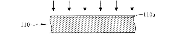
110a 活性化する領域
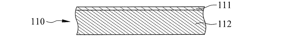
111 活性層
112 未活性層
113 混合層
114 第二載置部
114a 第二外囲面
115 第三溝
120 結合層
121 第一載置部
121a 第一外囲面
121b 表面
122 第二溝
130 回路層
131 回路
131a 第三外囲面
131b 上面
132 第一溝
140 接続層
141 第四外囲面
200 フォトレジスト層
210 開口部
300 接着剤
400 ガラス基板
D1 第一水平距離
D2 第二水平距離
L 縦方向延長線
S 横方向浸食溝
Claims (15)
- 底板と、結合層と、回路層とを含むパターン化する回路基板を有し、前記結合層は前記底板と前記回路層との間に位置され、前記底板は活性層及び未活性層を有し、前記底板は活性化処理を経て前記活性層が形成され、前記結合層の一部が前記活性層中に嵌入されることで、前記結合層が嵌入される前記活性層が混合層として形成される、パターン化する回路基板の提供工程と、
フォトレジスト層により前記回路層がマスクされるフォトレジスト層の形成工程と、
複数の開口部が形成され、これら前記開口部から前記回路層が露出される前記フォトレジスト層のパターン化工程と、
前記フォトレジスト層によりマスクされ、これら前記開口部から露出される前記回路層が除去され、前記回路層に複数の回路が形成され、隣接する2つの前記回路の間には第一溝を有し、前記第一溝から前記結合層が露出される、前記回路層のパターン化工程と、
前記フォトレジスト層の除去工程と、
これら前記回路をマスクとし、これら前記第一溝から露出されると共に前記活性層に嵌入される前記結合層が除去され、これら前記回路の下方に位置される前記結合層に複数の第一載置部が形成され、隣接する2つの前記第一載置部の間には第二溝を有し、前記第二溝から前記混合層が露出される前記結合層のパターン化工程と、
これら前記第一載置部によりマスクされ、これら前記第二溝から露出される前記混合層が除去され、これら前記第一載置部の下方に位置される前記混合層に複数の第二載置部が形成され、隣接する2つの前記第二載置部の間には第三溝を有し、前記第三溝から前記未活性層が露出される前記底板のパターン化工程と、を含むことを特徴とする回路基板の製造方法。 - 各前記第一載置部は第一外囲面を有し、各前記第二載置部は第二外囲面を有し、前記第二外囲面と、前記第一外囲面に沿う縦方向延長線との間には横方向浸食溝が形成され、前記横方向浸食溝は前記第一載置部の下方に位置されると共に前記第三溝に連通され、前記第二外囲面と前記縦方向延長線との間には第一水平距離を有することを特徴とする、請求項1に記載の回路基板の製造方法。
- 前記底板がパターン化された後には、これら前記回路にエッチングが施され、前記第一溝が拡大し、前記第一載置部の表面が露出されることを特徴とする、請求項2に記載の回路基板の製造方法。
- これら前記回路にエッチングが施された後には、接続層が各前記回路に形成され、エッチングが施された後の各前記回路は第三外囲面及び上面を有し、前記接続層により前記第三外囲面及び前記上面が被覆され、且つ前記接続層が前記第一載置部の前記表面に接触することで、各前記回路が前記第一載置部及び前記接続層で構成される空間中に被覆されることを特徴とする、請求項3に記載の回路基板の製造方法。
- 前記第三外囲面を被覆させる前記接続層は第四外囲面を有し、前記第四外囲面と前記縦方向延長線との間には第二水平距離を有することを特徴とする、請求項4に記載の回路基板の製造方法。
- 前記第二水平距離は前記第一水平距離より長いことを特徴とする、請求項5に記載の回路基板の製造方法。
- 前記第二水平距離と前記第一水平距離との差値は28〜158nmであることを特徴とする、請求項6に記載の回路基板の製造方法。
- 前記活性化処理はプラズマにより前記底板の活性化する領域の活性化を行って、前記活性化する領域に前記活性層が形成されることを特徴とする、請求項1に記載の回路基板の製造方法。
- 前記結合層は複数の金属粒子が前記活性層にスパッタリングされることで形成され、且つこれら前記金属粒子の一部が前記活性層中に嵌入され、前記混合層が形成されることを特徴とする、請求項1または8に記載の回路基板の製造方法。
- パターン化底板と、複数の第一載置部と、複数の回路とを備え、これら前記第一載置部は前記パターン化底板とこれら前記回路との間に位置され、且つこれら前記回路はこれら前記第一載置部に設置される回路基板であって、
前記パターン化底板は複数の第二載置部及び未活性層を有し、これら前記第二載置部はこれら前記第一載置部と前記未活性層との間に位置され、且つこれら前記第二載置部は前記未活性層に形成され、これら前記第二載置部は底板の混合層がパターン化されることで形成され、前記混合層は前記底板の活性層及び前記活性層に部分的に嵌入される結合層により形成され、隣接する2つの前記第二載置部の間には溝を有し、前記溝から前記未活性層が露出されることを特徴とする回路基板。 - 各前記第一載置部は第一外囲面を有し、各前記第二載置部は第二外囲面を有し、前記第二外囲面と、前記第一外囲面に沿う縦方向延長線との間には横方向浸食溝が形成され、前記横方向浸食溝は前記第一載置部の下方に位置されると共に前記溝に連通され、前記第二外囲面と前記縦方向延長線との間には第一水平距離を有することを特徴とする、請求項10に記載の回路基板。
- 各前記回路に形成される接続層を更に備え、各前記回路は第三外囲面及び上面を有し、前記接続層により前記第三外囲面及び前記上面が被覆され、且つ前記接続層が前記第一載置部の表面に接触することで、各前記回路が前記第一載置部及び前記接続層で構成される空間中にマスクされることを特徴とする、請求項11に記載の回路基板。
- 前記第三外囲面を被覆させる前記接続層は第四外囲面を有し、前記第四外囲面と前記縦方向延長線との間には第二水平距離を有することを特徴とする、請求項12に記載の回路基板。
- 前記第二水平距離は前記第一水平距離より長いことを特徴とする、請求項13に記載の回路基板。
- 前記第二水平距離と前記第一水平距離との差値は28〜158nmであることを特徴とする、請求項14に記載の回路基板。
Applications Claiming Priority (2)
| Application Number | Priority Date | Filing Date | Title |
|---|---|---|---|
| TW105108350 | 2016-03-17 | ||
| TW105108350A TWI595820B (zh) | 2016-03-17 | 2016-03-17 | 線路基板圖案化製程及線路基板 |
Publications (2)
| Publication Number | Publication Date |
|---|---|
| JP2017168794A true JP2017168794A (ja) | 2017-09-21 |
| JP6255054B2 JP6255054B2 (ja) | 2017-12-27 |
Family
ID=59904638
Family Applications (1)
| Application Number | Title | Priority Date | Filing Date |
|---|---|---|---|
| JP2016086926A Active JP6255054B2 (ja) | 2016-03-17 | 2016-04-25 | 回路基板の製造方法 |
Country Status (4)
| Country | Link |
|---|---|
| JP (1) | JP6255054B2 (ja) |
| KR (1) | KR101836298B1 (ja) |
| CN (1) | CN107205320B (ja) |
| TW (1) | TWI595820B (ja) |
Citations (2)
| Publication number | Priority date | Publication date | Assignee | Title |
|---|---|---|---|---|
| JPH0951163A (ja) * | 1995-05-31 | 1997-02-18 | Mitsui Toatsu Chem Inc | フレキシブル回路基板 |
| JP2009010398A (ja) * | 2003-12-05 | 2009-01-15 | Mitsui Mining & Smelting Co Ltd | プリント配線基板の製造方法 |
Family Cites Families (6)
| Publication number | Priority date | Publication date | Assignee | Title |
|---|---|---|---|---|
| TWI432110B (zh) * | 2008-03-28 | 2014-03-21 | Unimicron Technology Corp | 線路板及其製程 |
| TWI425895B (zh) * | 2008-12-11 | 2014-02-01 | Unimicron Technology Corp | 線路基板製程 |
| TWI417018B (zh) * | 2010-07-29 | 2013-11-21 | Unimicron Technology Corp | 線路板及其製造方法 |
| CN103052268B (zh) * | 2011-10-11 | 2016-03-02 | 欣兴电子股份有限公司 | 线路结构的制作方法 |
| JP2013153051A (ja) * | 2012-01-25 | 2013-08-08 | Tokuyama Corp | メタライズドセラミックスビア基板及びその製造方法 |
| TWI577257B (zh) * | 2014-12-24 | 2017-04-01 | 綠點高新科技股份有限公司 | 於基材絕緣表面形成導電線路的方法 |
-
2016
- 2016-03-17 TW TW105108350A patent/TWI595820B/zh active
- 2016-04-13 CN CN201610227095.XA patent/CN107205320B/zh active Active
- 2016-04-18 KR KR1020160047120A patent/KR101836298B1/ko active IP Right Grant
- 2016-04-25 JP JP2016086926A patent/JP6255054B2/ja active Active
Patent Citations (2)
| Publication number | Priority date | Publication date | Assignee | Title |
|---|---|---|---|---|
| JPH0951163A (ja) * | 1995-05-31 | 1997-02-18 | Mitsui Toatsu Chem Inc | フレキシブル回路基板 |
| JP2009010398A (ja) * | 2003-12-05 | 2009-01-15 | Mitsui Mining & Smelting Co Ltd | プリント配線基板の製造方法 |
Also Published As
| Publication number | Publication date |
|---|---|
| TW201735753A (zh) | 2017-10-01 |
| CN107205320B (zh) | 2020-03-17 |
| JP6255054B2 (ja) | 2017-12-27 |
| KR101836298B1 (ko) | 2018-03-08 |
| TWI595820B (zh) | 2017-08-11 |
| CN107205320A (zh) | 2017-09-26 |
| KR20170108734A (ko) | 2017-09-27 |
Similar Documents
| Publication | Publication Date | Title |
|---|---|---|
| JP2011040702A (ja) | コアレスパッケージ基板及びその製造方法 | |
| US7698813B2 (en) | Method for fabricating conductive blind via of circuit substrate | |
| JP6157968B2 (ja) | 配線回路基板およびその製造方法 | |
| JP2008141170A (ja) | 半導体装置およびその製造方法 | |
| TW201517710A (zh) | 電路板及電路板製作方法 | |
| KR20130133134A (ko) | 배선 기판 및 그 제조 방법 | |
| JP4624217B2 (ja) | 回路基板の製造方法 | |
| TWI425889B (zh) | 線路結構及其製作方法 | |
| TWI419627B (zh) | 線路板結構及其製作方法 | |
| JP6619294B2 (ja) | 配線基板及びその製造方法と電子部品装置 | |
| JP5815473B2 (ja) | 導電パターン形成基板の製造方法 | |
| JP6255054B2 (ja) | 回路基板の製造方法 | |
| JP2010232579A (ja) | プリント配線板の製造方法 | |
| TW201523798A (zh) | Ic載板、具有該ic載板的半導體器件及其製造方法 | |
| JP2011086681A (ja) | プリント基板の製造方法 | |
| TWI450656B (zh) | 電路板及其製作方法 | |
| TW201618621A (zh) | 電路板的製作方法 | |
| TW201625081A (zh) | 軟性電路板微孔徑導電通孔結構及製造方法 | |
| US20140069704A1 (en) | Method and structure for forming contact pads on a printed circuit board using zero under cut technology | |
| JP2008034472A (ja) | 半導体装置及びその製造方法 | |
| JP2008218871A (ja) | 電子部品の製造方法 | |
| TWI420993B (zh) | 電路板製作方法 | |
| JP2014130953A (ja) | 配線基板 | |
| JP2015012115A (ja) | 配線基板の製造方法 | |
| JP2015179758A (ja) | 半導体装置用リードフレーム及びその製造方法 |
Legal Events
| Date | Code | Title | Description |
|---|---|---|---|
| TRDD | Decision of grant or rejection written | ||
| A01 | Written decision to grant a patent or to grant a registration (utility model) |
Free format text: JAPANESE INTERMEDIATE CODE: A01 Effective date: 20171003 |
|
| A601 | Written request for extension of time |
Free format text: JAPANESE INTERMEDIATE CODE: A601 Effective date: 20171004 |
|
| A61 | First payment of annual fees (during grant procedure) |
Free format text: JAPANESE INTERMEDIATE CODE: A61 Effective date: 20171201 |
|
| R150 | Certificate of patent or registration of utility model |
Ref document number: 6255054 Country of ref document: JP Free format text: JAPANESE INTERMEDIATE CODE: R150 |
|
| R250 | Receipt of annual fees |
Free format text: JAPANESE INTERMEDIATE CODE: R250 |
|
| R250 | Receipt of annual fees |
Free format text: JAPANESE INTERMEDIATE CODE: R250 |
|
| R250 | Receipt of annual fees |
Free format text: JAPANESE INTERMEDIATE CODE: R250 |
|
| R250 | Receipt of annual fees |
Free format text: JAPANESE INTERMEDIATE CODE: R250 |