JP2017168794A - Manufacturing method of circuit board - Google Patents
Manufacturing method of circuit board Download PDFInfo
- Publication number
- JP2017168794A JP2017168794A JP2016086926A JP2016086926A JP2017168794A JP 2017168794 A JP2017168794 A JP 2017168794A JP 2016086926 A JP2016086926 A JP 2016086926A JP 2016086926 A JP2016086926 A JP 2016086926A JP 2017168794 A JP2017168794 A JP 2017168794A
- Authority
- JP
- Japan
- Prior art keywords
- layer
- circuit board
- circuit
- groove
- bottom plate
- Prior art date
- Legal status (The legal status is an assumption and is not a legal conclusion. Google has not performed a legal analysis and makes no representation as to the accuracy of the status listed.)
- Granted
Links
- 238000004519 manufacturing process Methods 0.000 title claims abstract description 35
- 229920002120 photoresistant polymer Polymers 0.000 claims abstract description 33
- 238000000059 patterning Methods 0.000 claims abstract description 30
- 230000008878 coupling Effects 0.000 claims abstract description 24
- 238000010168 coupling process Methods 0.000 claims abstract description 24
- 238000005859 coupling reaction Methods 0.000 claims abstract description 24
- 238000000034 method Methods 0.000 claims description 22
- 238000005530 etching Methods 0.000 claims description 14
- 230000003628 erosive effect Effects 0.000 claims description 8
- 238000001994 activation Methods 0.000 claims description 6
- 239000002923 metal particle Substances 0.000 claims description 4
- 238000004544 sputter deposition Methods 0.000 claims description 2
- 230000004913 activation Effects 0.000 abstract description 4
- 239000000853 adhesive Substances 0.000 description 25
- 230000001070 adhesive effect Effects 0.000 description 25
- 238000010586 diagram Methods 0.000 description 13
- 239000011521 glass Substances 0.000 description 7
- 230000002093 peripheral effect Effects 0.000 description 7
- 239000000758 substrate Substances 0.000 description 7
- VEXZGXHMUGYJMC-UHFFFAOYSA-N Hydrochloric acid Chemical compound Cl VEXZGXHMUGYJMC-UHFFFAOYSA-N 0.000 description 4
- KWYUFKZDYYNOTN-UHFFFAOYSA-M Potassium hydroxide Chemical compound [OH-].[K+] KWYUFKZDYYNOTN-UHFFFAOYSA-M 0.000 description 3
- HEMHJVSKTPXQMS-UHFFFAOYSA-M Sodium hydroxide Chemical compound [OH-].[Na+] HEMHJVSKTPXQMS-UHFFFAOYSA-M 0.000 description 3
- MHAJPDPJQMAIIY-UHFFFAOYSA-N Hydrogen peroxide Chemical compound OO MHAJPDPJQMAIIY-UHFFFAOYSA-N 0.000 description 2
- 230000015572 biosynthetic process Effects 0.000 description 2
- 238000005516 engineering process Methods 0.000 description 2
- 229910000041 hydrogen chloride Inorganic materials 0.000 description 2
- IXCSERBJSXMMFS-UHFFFAOYSA-N hydrogen chloride Substances Cl.Cl IXCSERBJSXMMFS-UHFFFAOYSA-N 0.000 description 2
- 230000000873 masking effect Effects 0.000 description 2
- 239000000463 material Substances 0.000 description 2
- QAOWNCQODCNURD-UHFFFAOYSA-N sulfuric acid group Chemical group S(O)(O)(=O)=O QAOWNCQODCNURD-UHFFFAOYSA-N 0.000 description 2
- 239000005749 Copper compound Substances 0.000 description 1
- GRYLNZFGIOXLOG-UHFFFAOYSA-N Nitric acid Chemical class O[N+]([O-])=O GRYLNZFGIOXLOG-UHFFFAOYSA-N 0.000 description 1
- 239000004642 Polyimide Substances 0.000 description 1
- 150000001880 copper compounds Chemical class 0.000 description 1
- KUNSUQLRTQLHQQ-UHFFFAOYSA-N copper tin Chemical class [Cu].[Sn] KUNSUQLRTQLHQQ-UHFFFAOYSA-N 0.000 description 1
- ORTQZVOHEJQUHG-UHFFFAOYSA-L copper(II) chloride Chemical compound Cl[Cu]Cl ORTQZVOHEJQUHG-UHFFFAOYSA-L 0.000 description 1
- 238000012217 deletion Methods 0.000 description 1
- 230000037430 deletion Effects 0.000 description 1
- 235000014113 dietary fatty acids Nutrition 0.000 description 1
- 238000009510 drug design Methods 0.000 description 1
- 239000000194 fatty acid Substances 0.000 description 1
- 229930195729 fatty acid Natural products 0.000 description 1
- 150000004665 fatty acids Chemical class 0.000 description 1
- 239000000945 filler Substances 0.000 description 1
- 150000002334 glycols Chemical class 0.000 description 1
- 230000003647 oxidation Effects 0.000 description 1
- 238000007254 oxidation reaction Methods 0.000 description 1
- 229920001515 polyalkylene glycol Polymers 0.000 description 1
- 229920001721 polyimide Polymers 0.000 description 1
- CHKVPAROMQMJNQ-UHFFFAOYSA-M potassium bisulfate Chemical compound [K+].OS([O-])(=O)=O CHKVPAROMQMJNQ-UHFFFAOYSA-M 0.000 description 1
- 229910000343 potassium bisulfate Inorganic materials 0.000 description 1
- 239000012286 potassium permanganate Substances 0.000 description 1
- KAQHZJVQFBJKCK-UHFFFAOYSA-L potassium pyrosulfate Chemical compound [K+].[K+].[O-]S(=O)(=O)OS([O-])(=O)=O KAQHZJVQFBJKCK-UHFFFAOYSA-L 0.000 description 1
- 238000007670 refining Methods 0.000 description 1
- XLYOFNOQVPJJNP-UHFFFAOYSA-N water Substances O XLYOFNOQVPJJNP-UHFFFAOYSA-N 0.000 description 1
Images


Classifications
-
- H—ELECTRICITY
- H05—ELECTRIC TECHNIQUES NOT OTHERWISE PROVIDED FOR
- H05K—PRINTED CIRCUITS; CASINGS OR CONSTRUCTIONAL DETAILS OF ELECTRIC APPARATUS; MANUFACTURE OF ASSEMBLAGES OF ELECTRICAL COMPONENTS
- H05K3/00—Apparatus or processes for manufacturing printed circuits
- H05K3/0073—Masks not provided for in groups H05K3/02 - H05K3/46, e.g. for photomechanical production of patterned surfaces
- H05K3/0079—Masks not provided for in groups H05K3/02 - H05K3/46, e.g. for photomechanical production of patterned surfaces characterised by the method of application or removal of the mask
-
- H—ELECTRICITY
- H05—ELECTRIC TECHNIQUES NOT OTHERWISE PROVIDED FOR
- H05K—PRINTED CIRCUITS; CASINGS OR CONSTRUCTIONAL DETAILS OF ELECTRIC APPARATUS; MANUFACTURE OF ASSEMBLAGES OF ELECTRICAL COMPONENTS
- H05K3/00—Apparatus or processes for manufacturing printed circuits
- H05K3/02—Apparatus or processes for manufacturing printed circuits in which the conductive material is applied to the surface of the insulating support and is thereafter removed from such areas of the surface which are not intended for current conducting or shielding
- H05K3/06—Apparatus or processes for manufacturing printed circuits in which the conductive material is applied to the surface of the insulating support and is thereafter removed from such areas of the surface which are not intended for current conducting or shielding the conductive material being removed chemically or electrolytically, e.g. by photo-etch process
-
- H—ELECTRICITY
- H01—ELECTRIC ELEMENTS
- H01L—SEMICONDUCTOR DEVICES NOT COVERED BY CLASS H10
- H01L23/00—Details of semiconductor or other solid state devices
- H01L23/12—Mountings, e.g. non-detachable insulating substrates
- H01L23/14—Mountings, e.g. non-detachable insulating substrates characterised by the material or its electrical properties
- H01L23/147—Semiconductor insulating substrates
-
- H—ELECTRICITY
- H05—ELECTRIC TECHNIQUES NOT OTHERWISE PROVIDED FOR
- H05K—PRINTED CIRCUITS; CASINGS OR CONSTRUCTIONAL DETAILS OF ELECTRIC APPARATUS; MANUFACTURE OF ASSEMBLAGES OF ELECTRICAL COMPONENTS
- H05K3/00—Apparatus or processes for manufacturing printed circuits
- H05K3/0011—Working of insulating substrates or insulating layers
- H05K3/0017—Etching of the substrate by chemical or physical means
- H05K3/0041—Etching of the substrate by chemical or physical means by plasma etching
-
- H—ELECTRICITY
- H05—ELECTRIC TECHNIQUES NOT OTHERWISE PROVIDED FOR
- H05K—PRINTED CIRCUITS; CASINGS OR CONSTRUCTIONAL DETAILS OF ELECTRIC APPARATUS; MANUFACTURE OF ASSEMBLAGES OF ELECTRICAL COMPONENTS
- H05K3/00—Apparatus or processes for manufacturing printed circuits
- H05K3/0073—Masks not provided for in groups H05K3/02 - H05K3/46, e.g. for photomechanical production of patterned surfaces
- H05K3/0082—Masks not provided for in groups H05K3/02 - H05K3/46, e.g. for photomechanical production of patterned surfaces characterised by the exposure method of radiation-sensitive masks
-
- H—ELECTRICITY
- H05—ELECTRIC TECHNIQUES NOT OTHERWISE PROVIDED FOR
- H05K—PRINTED CIRCUITS; CASINGS OR CONSTRUCTIONAL DETAILS OF ELECTRIC APPARATUS; MANUFACTURE OF ASSEMBLAGES OF ELECTRICAL COMPONENTS
- H05K3/00—Apparatus or processes for manufacturing printed circuits
- H05K3/22—Secondary treatment of printed circuits
- H05K3/28—Applying non-metallic protective coatings
-
- H—ELECTRICITY
- H05—ELECTRIC TECHNIQUES NOT OTHERWISE PROVIDED FOR
- H05K—PRINTED CIRCUITS; CASINGS OR CONSTRUCTIONAL DETAILS OF ELECTRIC APPARATUS; MANUFACTURE OF ASSEMBLAGES OF ELECTRICAL COMPONENTS
- H05K3/00—Apparatus or processes for manufacturing printed circuits
- H05K3/30—Assembling printed circuits with electric components, e.g. with resistor
- H05K3/32—Assembling printed circuits with electric components, e.g. with resistor electrically connecting electric components or wires to printed circuits
- H05K3/321—Assembling printed circuits with electric components, e.g. with resistor electrically connecting electric components or wires to printed circuits by conductive adhesives
- H05K3/323—Assembling printed circuits with electric components, e.g. with resistor electrically connecting electric components or wires to printed circuits by conductive adhesives by applying an anisotropic conductive adhesive layer over an array of pads
-
- H—ELECTRICITY
- H05—ELECTRIC TECHNIQUES NOT OTHERWISE PROVIDED FOR
- H05K—PRINTED CIRCUITS; CASINGS OR CONSTRUCTIONAL DETAILS OF ELECTRIC APPARATUS; MANUFACTURE OF ASSEMBLAGES OF ELECTRICAL COMPONENTS
- H05K2203/00—Indexing scheme relating to apparatus or processes for manufacturing printed circuits covered by H05K3/00
- H05K2203/13—Moulding and encapsulation; Deposition techniques; Protective layers
- H05K2203/1305—Moulding and encapsulation
Abstract
Description
本発明は、接着剤(例えば、非導電性ペースト(Non−conductive Paste)、導電性ペースト(conductivev Paste)等の充填接着剤)の付着力を高める回路基板の製造方法及び回路基板に関する。 The present invention relates to a method for manufacturing a circuit board and a circuit board for improving the adhesion of an adhesive (for example, a filling adhesive such as a non-conductive paste and a conductive paste).
従来の回路基板の製造工程では、先ず底板の表面に活性化処理を施し、後続の製造工程で回路を形成し易くする。 In the conventional circuit board manufacturing process, the surface of the bottom plate is first subjected to an activation process to facilitate the formation of a circuit in the subsequent manufacturing process.
しかしながら、前述した従来の技術では、すなわち、活性化処理が施された表面が異物を吸着させてしまい、接着剤(例えば、非導電性ペースト、導電性ペースト等の充填接着剤)が底板の表面に付着しにくくなり、回路基板及びガラス基板の結合強度の低下を招いた。このため、接着剤の底板表面への付着力を如何に高めるかが本分野で解決が待ち望まれる問題である。そこで、本発明者は上記の欠点が改善可能と考え、鋭意検討を重ねた結果、合理的設計で上記の課題を効果的に改善する本発明の提案に到った。 However, in the above-described conventional technology, that is, the surface subjected to the activation treatment adsorbs foreign matter, and an adhesive (for example, a filling adhesive such as a non-conductive paste or a conductive paste) is applied to the surface of the bottom plate. The adhesion strength between the circuit board and the glass substrate was lowered. Therefore, how to increase the adhesive force of the adhesive to the bottom plate surface is a problem that is desired to be solved in this field. Therefore, the present inventor considered that the above-mentioned drawbacks can be improved, and as a result of intensive studies, the present inventor has arrived at a proposal of the present invention that effectively improves the above-described problems by rational design.
本発明は、以上の従来技術の課題を解決する為になされたものである。即ち、本発明は、回路基板の製造方法及び回路基板を提供することを主目的とする。つまり、底板に異物が吸着して接着剤(例えば、非導電性ペースト、導電性ペースト等の充填接着剤)と底板との間の接合強度に影響を与えることによる、パッケージ構造の信頼性の低下を回避する。 The present invention has been made to solve the above-described problems of the prior art. That is, the main object of the present invention is to provide a circuit board manufacturing method and a circuit board. In other words, the reliability of the package structure is reduced due to foreign matter adsorbing on the bottom plate and affecting the bonding strength between the adhesive (for example, a filling adhesive such as non-conductive paste and conductive paste) and the bottom plate. To avoid.
上述した課題を解決し、目的を達成するために、本発明に係る回路基板の製造方法は、底板と、結合層と、回路層とを含むパターン化する回路基板を有し、結合層は底板と回路層との間に位置され、底板は活性層及び未活性層を有し、底板は活性化処理を経て活性層が形成され、結合層の一部が活性層中に嵌入されることで、結合層が嵌入される活性層が混合層として形成される、パターン化する回路基板の提供工程と、フォトレジスト層により回路層がマスクされるフォトレジスト層の形成工程と、複数の開口部が形成され、これら開口部から回路層が露出されるフォトレジスト層のパターン化工程と、フォトレジスト層によりマスクされ、これら開口部から露出される回路層が除去され、回路層に複数の回路が形成され、隣接する2つの回路の間には第一溝を有し、第一溝から結合層が露出される、回路層のパターン化工程と、フォトレジスト層の除去工程と、これら回路をマスクとし、これら第一溝から露出されると共に活性層に嵌入される結合層が除去され、これら回路の下方に位置される結合層に複数の第一載置部が形成され、隣接する2つの第一載置部の間には第二溝を有し、第二溝から混合層が露出される結合層のパターン化工程と、第一載置部によりマスクされ、これら第二溝から露出される混合層が除去され、これら第一載置部の下方に位置される混合層に複数の第二載置部が形成され、隣接する2つの第二載置部の間には第三溝を有し、第三溝から未活性層が露出される底板のパターン化工程とを含む。 In order to solve the above-mentioned problems and achieve the object, a circuit board manufacturing method according to the present invention includes a circuit board to be patterned including a bottom plate, a coupling layer, and a circuit layer, and the coupling layer is a bottom plate. The bottom plate has an active layer and an inactive layer. The bottom plate is activated to form an active layer, and a part of the coupling layer is inserted into the active layer. A step of providing a circuit board to be patterned, wherein the active layer into which the bonding layer is inserted is formed as a mixed layer, a step of forming a photoresist layer in which the circuit layer is masked by the photoresist layer, and a plurality of openings Forming a photoresist layer patterning process in which the circuit layers are exposed from the openings, and masking the photoresist layer to remove the circuit layers exposed from the opening parts, thereby forming a plurality of circuits in the circuit layer Two adjacent A circuit layer patterning step, a photoresist layer removing step, and a first layer having a first groove between the paths and exposing the coupling layer from the first groove, and using the circuit as a mask, from the first groove The bonding layer that is exposed and fitted into the active layer is removed, and a plurality of first mounting portions are formed in the bonding layer located below these circuits, and between the two adjacent first mounting portions. Has a second groove, a bonding layer patterning process in which the mixed layer is exposed from the second groove, masked by the first mounting portion, and the mixed layer exposed from these second grooves is removed, A plurality of second placement portions are formed in the mixed layer located below the first placement portion, and a third groove is provided between two adjacent second placement portions, and the third groove is not yet formed. Patterning a bottom plate from which the active layer is exposed.
本発明はこれら第二溝から露出される混合層が除去されることで、異物が吸着し易い混合層が接着剤(例えば、非導電性ペースト、導電性ペースト等充填接着剤)の付着力に影響を与え、回路基板及びガラス基板のパッケージングの際に、接着剤と回路基板との間の接合強度が不足してパッケージ構造の歩留りが低下する事態の発生を回避させる。 In the present invention, the mixed layer exposed from these second grooves is removed, so that a mixed layer that easily adsorbs foreign matters is attached to the adhesive force of the adhesive (for example, non-conductive paste, conductive paste, etc.). This affects the occurrence of a situation where the bonding strength between the adhesive and the circuit board is insufficient and the yield of the package structure is lowered when the circuit board and the glass substrate are packaged.
本発明における好適な実施形態について、添付図面を参照して説明する。尚、以下に説明する実施形態は、特許請求の範囲に記載された本発明の内容を限定するものではない。また、以下に説明される構成の全てが、本発明の必須要件であるとは限らない。 Preferred embodiments of the present invention will be described with reference to the accompanying drawings. In addition, embodiment described below does not limit the content of this invention described in the claim. In addition, all of the configurations described below are not necessarily essential requirements of the present invention.
(一実施形態)
以下、一実施形態を図1〜14に基づいて説明する。本発明の回路基板の製造方法10は、パターン化する回路基板の提供工程11と、フォトレジスト層の形成工程12と、フォトレジスト層のパターン化工程13と、回路層のパターン化工程14と、フォトレジスト層の削除工程15と、接合層のパターン化工程16と、底板のパターン化工程17とを含む(図1参照)。
(One embodiment)
Hereinafter, an embodiment will be described with reference to FIGS. The circuit
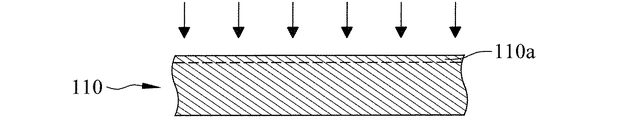
パターン化する回路基板の提供工程11では、底板110と、結合層120と、回路層130とを有するパターン化する回路基板100が提供され、結合層120は底板110と回路層130との間に位置される。本実施形態によると、底板110の材質はポリイミドである(図1及び図5参照)。
In
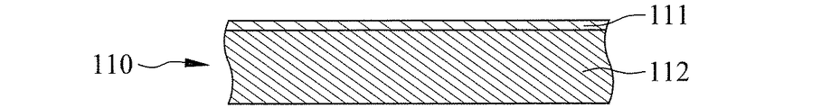
図2乃至図4は、パターン化する回路基板100の製造方法のフローチャートを示す。まず、図3に示すように、底板110は活性化処理により活性層111及び未活性層112が形成され、活性層111により結合層120の付着力が強化される。図2を参照すると、本実施形態では、活性化処理はプラズマにより底板110の活性化する領域110aが活性化されることで、活性化する領域110aに活性層111が形成される。続いて、図4に示すように、結合層120が底板110に形成され、結合層120により活性層111がマスクされ、且つ結合層120の一部が活性層111中に嵌入されることで、結合層120が嵌入される活性層111に混合層113が形成される。本実施形態において、結合層120は複数の金属粒子が活性層111にスパッタリングされることで形成され、且つこれら金属粒子の一部が活性層111中に嵌入されて、混合層113が形成される。最後に、図5に示すように、回路層130が結合層120に形成され、パターン化する回路基板100が形成される。
2 to 4 show flowcharts of a method of manufacturing the
フォトレジスト層の形成工程12では、フォトレジスト層200が回路層130に形成され、フォトレジスト層200により回路層130がマスクされる(図1及び図6参照)。
In the photoresist
フォトレジスト層のパターン化工程13では、露光と現像等の製造工程によりフォトレジスト層200に複数の開口部210が形成され、これら開口部210から回路層130が露出される(図1及び図7参照)。
In the photoresist
また、回路層のパターン化工程14では、フォトレジスト層200をマスクとし、これら開口部210から露出される回路層130が除去されることで、回路層130に複数の回路131が形成される。隣接する2つの回路131の間には第一溝132を有し、第一溝132からは結合層120が露出される。本実施形態において、第一エッチング液により回路層130のエッチングが行われて、これら開口部210から露出される回路層130が除去される。第一エッチング液の主要成分は塩化水素及び塩化銅を含む(図1及び図8参照)。
Further, in the circuit layer patterning
図1及び図9に示すように、フォトレジスト層の削除工程15では、フォトレジスト層200が削除され、これら回路131が露出される。本実施形態によると、水酸化カリウムを含有する精錬液によりフォトレジスト層200が削除される。
As shown in FIGS. 1 and 9, in the photoresist
なお、図1及び図10に示すように、接合層のパターン化工程16では、これら回路131をマスクとし、これら第一溝132から露出されると共に活性層111に嵌入しない結合層120が除去されることで、これら回路131の下方に位置される結合層120に複数の第一載置部121が形成され、隣接する2つの第一載置部121の間には第二溝122を有し、第二溝122からは混合層113が露出される。本実施形態において、第二エッチング液により結合層120のエッチングが行われて、これら第一溝132から露出されると共に活性層111に嵌入しない結合層120が除去される。第二エッチング液の主要成分は塩化水素と、銅化合物と、硝酸誘導体と、脂肪酸誘導体と、ポリアルキレングリコール誘導体とを含む。
As shown in FIGS. 1 and 10, in the bonding
図1及び図11に示すように、底板のパターン化工程17では、これら第一載置部121をマスクとし、これら第二溝122から露出される混合層113が除去されることで、これら第一載置部121の下方に位置される混合層113に複数の第二載置部114が形成され、且つ底板110にパターン化底板110’が形成される。隣接する2つの第二載置部114の間には第三溝115を有し、第三溝115から底板110の未活性層112が露出される。本実施形態において、等方性エッチング液により底板110のエッチングが行われて、これら第二溝122から露出される混合層113が除去される。等方性エッチング液は過マンガン酸カリウム或いは水酸化ナトリウムの内から選択される。
As shown in FIGS. 1 and 11, in the bottom
パターン化する回路基板100は、工程11から工程17の処理を経て回路基板100’が形成され、回路基板100’はパターン化底板110’と、これら第一載置部121と、これら回路131とを備える。これら第一載置部121はパターン化底板110’とこれら回路131との間に位置され、且つこれら回路131はこれら第一載置部121に設置される。パターン化底板110’はこれら第二載置部114及び未活性層112を含み、これら第二載置部114はこれら第一載置部121と未活性層112との間にそれぞれ位置され、且つこれら第二載置部114は未活性層112に形成される(図11参照)。
The
次は、図11に示すように、本実施形態において、各第一載置部121は第一外囲面121aを有し、各第二載置部114は第二外囲面114aを有する。底板のパターン化110過程では、等方性エッチングにより第二外囲面114aと第一外囲面121aに沿う縦方向延長線Lとの間に横方向浸食溝Sが形成され、横方向浸食溝Sは第一載置部121の下方に位置されると共に第三溝115に連通される。第二外囲面114aと縦方向延長線Lとの間には第一水平距離D1を有し、第一水平距離D1は第二外囲面114aと縦方向延長線Lとの最短距離である。
Next, as shown in FIG. 11, in this embodiment, each
図1及び図12に示すように、本実施形態において、底板のパターン化110の後には回路のエッチング工程18を更に含む。回路のエッチング工程18では、これら回路131にエッチングが施されることで、第一溝132が拡大して第一載置部121の表面121bが露出される。エッチング後の各回路131は第三外囲面131a及び上面131bを有し、本実施形態において、第三エッチング液によりこれら回路131のエッチングが行われる。第三エッチング液の主要成分は、硫酸水素カリウムと、二硫酸カリウムと、無機塩酸とを含む。或いは、他の実施形態では、第三エッチング液は硫酸或いは過酸化水素水の内から選択される。
As shown in FIGS. 1 and 12, in this embodiment, a
図1及び図13に示すように、本実施形態において、これら回路131のエッチング後には接続層の形成工程19を更に含む。接続層の形成工程19では、接続層140が各回路131に形成され、接続層140により各回路131の第三外囲面131a及び上面131bが被覆され、且つ接続層140が第一載置部121の表面121bに接触することで、各回路131が第一載置部121及び接続層140で構成される空間中に被覆され、これら回路131の酸化が防止される。本実施形態において、接続層140の材質は銅錫合金である。
As shown in FIGS. 1 and 13, in the present embodiment, a connection
第三外囲面131aを被覆させる接続層140は第四外囲面141を有し、第四外囲面141と縦方向延長線Lとの間には第二水平距離D2を有する。第二水平距離D2は第四外囲面141と縦方向延長線Lとの最短距離である(図13参照)。本実施形態において、第二水平距離D2は第一水平距離D1より長いため、横方向浸食溝Sに累積される水気が結合層120を経て回路層130中に浸透することでショートが発生する事態が回避される。好ましくは、第二水平距離D2と第一水平距離D1との差値は28〜158nmである。
The
本発明の回路基板100’は接着剤300(例えば、非導電性ペースト、導電性ペースト等の充填接着剤)及びガラス基板400によりパッケージングが行われる(図13参照)。本実施形態において、接着剤300は異方性導電性ペースト(ACF)であり、このため接着剤300が回路基板100’及びガラス基板400に接合され、且つ回路基板100’のこれら回路131及びガラス基板400の電極(図示せず)が電気的に接続され、接着剤300の付着力のためにパッケージ構造の信頼性が高まる。これにより、本発明は底板のパターン化110により露出される混合層113が除去されることで、混合層113に異物が吸着して接着剤300及び回路基板100’の間の接合強度に影響が及ぶのを回避させる。更には、本発明は等方性エッチングにより発生する横方向浸食溝Sに接着剤300が設置され、接着剤300の付着力が更に高まる。
The
従って、本明細書に開示された実施形態は、本発明を限定するものではなく、説明するためのものであり、このような実施形態によって本発明の思想と範囲が限定されるものではない。本発明の範囲は特許請求の範囲により解釈すべきであり、それと同等の範囲内にある全ての技術は、本発明の権利範囲に含まれるものと解釈すべきである。 Accordingly, the embodiments disclosed herein are for the purpose of explaining, not limiting the present invention, and the spirit and scope of the present invention are not limited by such embodiments. The scope of the present invention should be construed according to the claims, and all technologies within the equivalent scope should be construed as being included in the scope of the present invention.
10 回路基板の製造方法
11 パターン化する回路基板の提供工程
12 フォトレジスト層の形成工程
13 フォトレジスト層のパターン化工程
14 回路層のパターン化工程
15 フォトレジスト層の削除工程
16 接合層のパターン化工程
17 底板のパターン化工程
18 回路のエッチング工程
19 接続層の形成工程
100 パターン化する回路基板
100’ 回路基板
110 底板
110’ パターン化底板
110a 活性化する領域
111 活性層
112 未活性層
113 混合層
114 第二載置部
114a 第二外囲面
115 第三溝
120 結合層
121 第一載置部
121a 第一外囲面
121b 表面
122 第二溝
130 回路層
131 回路
131a 第三外囲面
131b 上面
132 第一溝
140 接続層
141 第四外囲面
200 フォトレジスト層
210 開口部
300 接着剤
400 ガラス基板
D1 第一水平距離
D2 第二水平距離
L 縦方向延長線
S 横方向浸食溝
DESCRIPTION OF
121a first
本発明は、接着剤(例えば、非導電性ペースト(Non−conductive Paste)、導電性ペースト(conductivev Paste)等の充填接着剤)の付着力を高める回路基板の製造方法に関する。 The present invention is an adhesive (e.g., non-conductive paste (Non-Conductive Paste), conductive paste (Conductivev Paste) filler adhesive, etc.) relates to the production how the circuit board to enhance the adhesion of.
上述した課題を解決し、目的を達成するために、本発明に係る回路基板の製造方法は、底板と、結合層と、回路層とを含むパターン化する回路基板を有し、結合層は底板と回路層との間に位置され、底板は活性層及び未活性層を有し、底板は活性化処理を経て活性層が形成され、結合層の一部が活性層中に嵌入されることで、結合層が嵌入される活性層が混合層として形成される、パターン化する回路基板の提供工程と、フォトレジスト層により回路層がマスクされるフォトレジスト層の形成工程と、複数の開口部が形成され、これら開口部から回路層が露出されるフォトレジスト層のパターン化工程と、フォトレジスト層によりマスクされ、これら開口部から露出される回路層が除去され、回路層に複数の回路が形成され、隣接する2つの回路の間には第一溝を有し、第一溝から結合層が露出される、回路層のパターン化工程と、フォトレジスト層の除去工程と、これら回路をマスクとし、これら第一溝から露出されると共に活性層に嵌入される結合層が除去され、これら回路の下方に位置される結合層に複数の第一載置部が形成され、隣接する2つの第一載置部の間には第二溝を有し、第二溝から混合層が露出される結合層のパターン化工程と、第一載置部によりマスクされ、これら第二溝から露出される混合層が除去され、これら第一載置部の下方に位置される混合層に複数の第二載置部が形成され、隣接する2つの第二載置部の間には第三溝を有し、第三溝から未活性層が露出される底板のパターン化工程とを含む。底板がパターン化された後には、これら回路にエッチングが施され、第一溝が拡大し、第一載置部の表面が露出される。
In order to solve the above-mentioned problems and achieve the object, a circuit board manufacturing method according to the present invention includes a circuit board to be patterned including a bottom plate, a coupling layer, and a circuit layer, and the coupling layer is a bottom plate. The bottom plate has an active layer and an inactive layer. The bottom plate is activated to form an active layer, and a part of the coupling layer is inserted into the active layer. A step of providing a circuit board to be patterned, wherein the active layer into which the bonding layer is inserted is formed as a mixed layer, a step of forming a photoresist layer in which the circuit layer is masked by the photoresist layer, and a plurality of openings Forming a photoresist layer patterning process in which the circuit layers are exposed from the openings, and masking the photoresist layer to remove the circuit layers exposed from the opening parts, thereby forming a plurality of circuits in the circuit layer Two adjacent A circuit layer patterning step, a photoresist layer removing step, and a first layer having a first groove between the paths and exposing the coupling layer from the first groove, and using the circuit as a mask, from the first groove The bonding layer that is exposed and fitted into the active layer is removed, and a plurality of first mounting portions are formed in the bonding layer located below these circuits, and between the two adjacent first mounting portions. Has a second groove, a bonding layer patterning process in which the mixed layer is exposed from the second groove, masked by the first mounting portion, and the mixed layer exposed from these second grooves is removed, A plurality of second placement portions are formed in the mixed layer located below the first placement portion, and a third groove is provided between two adjacent second placement portions, and the third groove is not yet formed. Patterning a bottom plate from which the active layer is exposed. After the bottom plate is patterned, these circuits are etched, the first groove is enlarged, and the surface of the first mounting portion is exposed.
Claims (15)
フォトレジスト層により前記回路層がマスクされるフォトレジスト層の形成工程と、
複数の開口部が形成され、これら前記開口部から前記回路層が露出される前記フォトレジスト層のパターン化工程と、
前記フォトレジスト層によりマスクされ、これら前記開口部から露出される前記回路層が除去され、前記回路層に複数の回路が形成され、隣接する2つの前記回路の間には第一溝を有し、前記第一溝から前記結合層が露出される、前記回路層のパターン化工程と、
前記フォトレジスト層の除去工程と、
これら前記回路をマスクとし、これら前記第一溝から露出されると共に前記活性層に嵌入される前記結合層が除去され、これら前記回路の下方に位置される前記結合層に複数の第一載置部が形成され、隣接する2つの前記第一載置部の間には第二溝を有し、前記第二溝から前記混合層が露出される前記結合層のパターン化工程と、
これら前記第一載置部によりマスクされ、これら前記第二溝から露出される前記混合層が除去され、これら前記第一載置部の下方に位置される前記混合層に複数の第二載置部が形成され、隣接する2つの前記第二載置部の間には第三溝を有し、前記第三溝から前記未活性層が露出される前記底板のパターン化工程と、を含むことを特徴とする回路基板の製造方法。 A circuit board to be patterned including a bottom plate, a coupling layer, and a circuit layer, wherein the coupling layer is located between the bottom plate and the circuit layer, and the bottom plate has an active layer and an inactive layer; The bottom plate is subjected to an activation process to form the active layer, and a part of the coupling layer is inserted into the active layer, whereby the active layer into which the coupling layer is inserted is formed as a mixed layer. Providing a circuit board to be patterned;
Forming a photoresist layer in which the circuit layer is masked by a photoresist layer;
A patterning step of the photoresist layer in which a plurality of openings are formed, and the circuit layer is exposed from the openings;
The circuit layer masked by the photoresist layer and exposed from the openings is removed, a plurality of circuits are formed in the circuit layer, and a first groove is provided between two adjacent circuits. Patterning the circuit layer, wherein the coupling layer is exposed from the first groove;
Removing the photoresist layer;
Using the circuit as a mask, the coupling layer exposed from the first groove and fitted into the active layer is removed, and a plurality of first mountings are disposed on the coupling layer positioned below the circuit. A bonding layer patterning step in which a portion is formed and has a second groove between two adjacent first mounting portions, and the mixed layer is exposed from the second groove;
The mixed layer masked by the first mounting portion and exposed from the second groove is removed, and a plurality of second mounting portions are disposed on the mixed layer positioned below the first mounting portion. A step of patterning the bottom plate having a third groove between two adjacent second mounting parts, and exposing the inactive layer from the third groove. A method of manufacturing a circuit board characterized by the above.
前記パターン化底板は複数の第二載置部及び未活性層を有し、これら前記第二載置部はこれら前記第一載置部と前記未活性層との間に位置され、且つこれら前記第二載置部は前記未活性層に形成され、これら前記第二載置部は底板の混合層がパターン化されることで形成され、前記混合層は前記底板の活性層及び前記活性層に部分的に嵌入される結合層により形成され、隣接する2つの前記第二載置部の間には溝を有し、前記溝から前記未活性層が露出されることを特徴とする回路基板。 A patterned bottom plate, a plurality of first mounting portions, and a plurality of circuits, wherein the first mounting portions are located between the patterned bottom plate and the circuits, and the circuits are A circuit board installed on the first mounting part,
The patterned bottom plate has a plurality of second placement portions and an inactive layer, and the second placement portions are located between the first placement portion and the inactive layer, and The second placement part is formed on the inactive layer, and the second placement part is formed by patterning a mixed layer of the bottom plate, and the mixed layer is formed on the active layer and the active layer of the bottom plate. A circuit board, which is formed by a bonding layer partially inserted, has a groove between two adjacent second mounting portions, and the inactive layer is exposed from the groove.
Applications Claiming Priority (2)
| Application Number | Priority Date | Filing Date | Title |
|---|---|---|---|
| TW105108350 | 2016-03-17 | ||
| TW105108350A TWI595820B (en) | 2016-03-17 | 2016-03-17 | Pattering process of circuit substrate and circuit substrate |
Publications (2)
| Publication Number | Publication Date |
|---|---|
| JP2017168794A true JP2017168794A (en) | 2017-09-21 |
| JP6255054B2 JP6255054B2 (en) | 2017-12-27 |
Family
ID=59904638
Family Applications (1)
| Application Number | Title | Priority Date | Filing Date |
|---|---|---|---|
| JP2016086926A Active JP6255054B2 (en) | 2016-03-17 | 2016-04-25 | Circuit board manufacturing method |
Country Status (4)
| Country | Link |
|---|---|
| JP (1) | JP6255054B2 (en) |
| KR (1) | KR101836298B1 (en) |
| CN (1) | CN107205320B (en) |
| TW (1) | TWI595820B (en) |
Citations (2)
| Publication number | Priority date | Publication date | Assignee | Title |
|---|---|---|---|---|
| JPH0951163A (en) * | 1995-05-31 | 1997-02-18 | Mitsui Toatsu Chem Inc | Flexible circuit board |
| JP2009010398A (en) * | 2003-12-05 | 2009-01-15 | Mitsui Mining & Smelting Co Ltd | Method of manufacturing printed wiring board |
Family Cites Families (6)
| Publication number | Priority date | Publication date | Assignee | Title |
|---|---|---|---|---|
| TWI432110B (en) * | 2008-03-28 | 2014-03-21 | Unimicron Technology Corp | Circuit board and fabricating process thereof |
| TWI425895B (en) * | 2008-12-11 | 2014-02-01 | Unimicron Technology Corp | Manufacturing process of circuit substrate |
| TWI417018B (en) * | 2010-07-29 | 2013-11-21 | Unimicron Technology Corp | Circuit board and manufacturing method thereof |
| CN103052268B (en) * | 2011-10-11 | 2016-03-02 | 欣兴电子股份有限公司 | The manufacture method of line construction |
| JP2013153051A (en) * | 2012-01-25 | 2013-08-08 | Tokuyama Corp | Metallized ceramic via substrate and manufacturing method thereof |
| TWI577257B (en) * | 2014-12-24 | 2017-04-01 | 綠點高新科技股份有限公司 | Method of forming conductive lines on an insulating surface of a substrate |
-
2016
- 2016-03-17 TW TW105108350A patent/TWI595820B/en active
- 2016-04-13 CN CN201610227095.XA patent/CN107205320B/en active Active
- 2016-04-18 KR KR1020160047120A patent/KR101836298B1/en active IP Right Grant
- 2016-04-25 JP JP2016086926A patent/JP6255054B2/en active Active
Patent Citations (2)
| Publication number | Priority date | Publication date | Assignee | Title |
|---|---|---|---|---|
| JPH0951163A (en) * | 1995-05-31 | 1997-02-18 | Mitsui Toatsu Chem Inc | Flexible circuit board |
| JP2009010398A (en) * | 2003-12-05 | 2009-01-15 | Mitsui Mining & Smelting Co Ltd | Method of manufacturing printed wiring board |
Also Published As
| Publication number | Publication date |
|---|---|
| KR20170108734A (en) | 2017-09-27 |
| KR101836298B1 (en) | 2018-03-08 |
| CN107205320B (en) | 2020-03-17 |
| CN107205320A (en) | 2017-09-26 |
| TWI595820B (en) | 2017-08-11 |
| TW201735753A (en) | 2017-10-01 |
| JP6255054B2 (en) | 2017-12-27 |
Similar Documents
| Publication | Publication Date | Title |
|---|---|---|
| JP2011040702A (en) | Coreless package substrate, and method of manufacturing the same | |
| US7698813B2 (en) | Method for fabricating conductive blind via of circuit substrate | |
| JP6157968B2 (en) | Wiring circuit board and manufacturing method thereof | |
| JP2008141170A (en) | Semiconductor device and its manufacturing method | |
| TW201517710A (en) | Circuit board and method for manufacturing same | |
| KR20130133134A (en) | Wiring board and method of manufacturing the same | |
| JP4624217B2 (en) | Circuit board manufacturing method | |
| TWI425889B (en) | Circuit structure and manufacturing method thereof | |
| JP6619294B2 (en) | WIRING BOARD, MANUFACTURING METHOD THEREOF, AND ELECTRONIC COMPONENT DEVICE | |
| JP5815473B2 (en) | Manufacturing method of conductive pattern forming substrate | |
| TW201316859A (en) | Circuit board structure and manufacturing method thereof | |
| JP6255054B2 (en) | Circuit board manufacturing method | |
| JP2010232579A (en) | Method of manufacturing printed wiring board | |
| JP2011086681A (en) | Method of manufacturing printed board | |
| TWI450656B (en) | Printed circuit board and method for manufacturing same | |
| TW201618621A (en) | Method for manufacturing printed circuit board | |
| TW201523798A (en) | IC substrate, semiconductor device with IC substrate and manufucturing method thereof | |
| TW201625081A (en) | Micro-aperture conductive via structure of flexible circuit board and manufacturing method thereof | |
| US20140069704A1 (en) | Method and structure for forming contact pads on a printed circuit board using zero under cut technology | |
| JP2008034472A (en) | Semiconductor device and method for manufacturing same | |
| JP2008218871A (en) | Electronic component manufacturing method | |
| TWI420993B (en) | Method for manufacturing printed circuit board | |
| JP2014130953A (en) | Wiring board | |
| JP2017103350A (en) | Printed-wiring board and method for manufacturing the same | |
| JP2015012115A (en) | Wiring board manufacturing method |
Legal Events
| Date | Code | Title | Description |
|---|---|---|---|
| TRDD | Decision of grant or rejection written | ||
| A01 | Written decision to grant a patent or to grant a registration (utility model) |
Free format text: JAPANESE INTERMEDIATE CODE: A01 Effective date: 20171003 |
|
| A601 | Written request for extension of time |
Free format text: JAPANESE INTERMEDIATE CODE: A601 Effective date: 20171004 |
|
| A61 | First payment of annual fees (during grant procedure) |
Free format text: JAPANESE INTERMEDIATE CODE: A61 Effective date: 20171201 |
|
| R150 | Certificate of patent or registration of utility model |
Ref document number: 6255054 Country of ref document: JP Free format text: JAPANESE INTERMEDIATE CODE: R150 |
|
| R250 | Receipt of annual fees |
Free format text: JAPANESE INTERMEDIATE CODE: R250 |
|
| R250 | Receipt of annual fees |
Free format text: JAPANESE INTERMEDIATE CODE: R250 |
|
| R250 | Receipt of annual fees |
Free format text: JAPANESE INTERMEDIATE CODE: R250 |
|
| R250 | Receipt of annual fees |
Free format text: JAPANESE INTERMEDIATE CODE: R250 |