JP2017146449A - 液晶表示装置 - Google Patents
液晶表示装置 Download PDFInfo
- Publication number
- JP2017146449A JP2017146449A JP2016027833A JP2016027833A JP2017146449A JP 2017146449 A JP2017146449 A JP 2017146449A JP 2016027833 A JP2016027833 A JP 2016027833A JP 2016027833 A JP2016027833 A JP 2016027833A JP 2017146449 A JP2017146449 A JP 2017146449A
- Authority
- JP
- Japan
- Prior art keywords
- liquid crystal
- contact hole
- insulating film
- crystal display
- display device
- Prior art date
- Legal status (The legal status is an assumption and is not a legal conclusion. Google has not performed a legal analysis and makes no representation as to the accuracy of the status listed.)
- Granted
Links
- 239000004973 liquid crystal related substance Substances 0.000 title claims abstract description 61
- 239000000758 substrate Substances 0.000 claims abstract description 52
- 239000000463 material Substances 0.000 claims description 27
- 229910052751 metal Inorganic materials 0.000 claims description 17
- 239000002184 metal Substances 0.000 claims description 17
- 239000011368 organic material Substances 0.000 claims description 2
- 239000000126 substance Substances 0.000 claims 3
- 239000010408 film Substances 0.000 description 212
- 238000002161 passivation Methods 0.000 description 72
- 239000010410 layer Substances 0.000 description 28
- 239000004065 semiconductor Substances 0.000 description 15
- 125000006850 spacer group Chemical group 0.000 description 14
- 239000011229 interlayer Substances 0.000 description 11
- 239000003990 capacitor Substances 0.000 description 10
- 238000000034 method Methods 0.000 description 10
- 239000011159 matrix material Substances 0.000 description 9
- 238000005229 chemical vapour deposition Methods 0.000 description 5
- 230000000694 effects Effects 0.000 description 5
- 238000000206 photolithography Methods 0.000 description 5
- 229910004298 SiO 2 Inorganic materials 0.000 description 3
- 230000015572 biosynthetic process Effects 0.000 description 3
- 239000007788 liquid Substances 0.000 description 3
- 229910021420 polycrystalline silicon Inorganic materials 0.000 description 3
- 239000011347 resin Substances 0.000 description 3
- 229920005989 resin Polymers 0.000 description 3
- 239000004925 Acrylic resin Substances 0.000 description 2
- 229920000178 Acrylic resin Polymers 0.000 description 2
- BOTDANWDWHJENH-UHFFFAOYSA-N Tetraethyl orthosilicate Chemical compound CCO[Si](OCC)(OCC)OCC BOTDANWDWHJENH-UHFFFAOYSA-N 0.000 description 2
- 238000010586 diagram Methods 0.000 description 2
- 239000011521 glass Substances 0.000 description 2
- 230000001846 repelling effect Effects 0.000 description 2
- 239000003566 sealing material Substances 0.000 description 2
- 238000004544 sputter deposition Methods 0.000 description 2
- 229910000838 Al alloy Inorganic materials 0.000 description 1
- 229910021417 amorphous silicon Inorganic materials 0.000 description 1
- 230000003064 anti-oxidating effect Effects 0.000 description 1
- 230000004888 barrier function Effects 0.000 description 1
- 230000005540 biological transmission Effects 0.000 description 1
- 230000007423 decrease Effects 0.000 description 1
- 230000005684 electric field Effects 0.000 description 1
- 239000003822 epoxy resin Substances 0.000 description 1
- 238000007687 exposure technique Methods 0.000 description 1
- 239000012535 impurity Substances 0.000 description 1
- AMGQUBHHOARCQH-UHFFFAOYSA-N indium;oxotin Chemical compound [In].[Sn]=O AMGQUBHHOARCQH-UHFFFAOYSA-N 0.000 description 1
- 238000005224 laser annealing Methods 0.000 description 1
- 239000000203 mixture Substances 0.000 description 1
- 229920002120 photoresistant polymer Polymers 0.000 description 1
- 229920000647 polyepoxide Polymers 0.000 description 1
- 229920001721 polyimide Polymers 0.000 description 1
- 239000009719 polyimide resin Substances 0.000 description 1
- 229920002050 silicone resin Polymers 0.000 description 1
- 239000010409 thin film Substances 0.000 description 1
- 238000002834 transmittance Methods 0.000 description 1
Images


Classifications
-
- G—PHYSICS
- G02—OPTICS
- G02F—OPTICAL DEVICES OR ARRANGEMENTS FOR THE CONTROL OF LIGHT BY MODIFICATION OF THE OPTICAL PROPERTIES OF THE MEDIA OF THE ELEMENTS INVOLVED THEREIN; NON-LINEAR OPTICS; FREQUENCY-CHANGING OF LIGHT; OPTICAL LOGIC ELEMENTS; OPTICAL ANALOGUE/DIGITAL CONVERTERS
- G02F1/00—Devices or arrangements for the control of the intensity, colour, phase, polarisation or direction of light arriving from an independent light source, e.g. switching, gating or modulating; Non-linear optics
- G02F1/01—Devices or arrangements for the control of the intensity, colour, phase, polarisation or direction of light arriving from an independent light source, e.g. switching, gating or modulating; Non-linear optics for the control of the intensity, phase, polarisation or colour
- G02F1/13—Devices or arrangements for the control of the intensity, colour, phase, polarisation or direction of light arriving from an independent light source, e.g. switching, gating or modulating; Non-linear optics for the control of the intensity, phase, polarisation or colour based on liquid crystals, e.g. single liquid crystal display cells
- G02F1/133—Constructional arrangements; Operation of liquid crystal cells; Circuit arrangements
- G02F1/1333—Constructional arrangements; Manufacturing methods
- G02F1/1337—Surface-induced orientation of the liquid crystal molecules, e.g. by alignment layers
-
- G—PHYSICS
- G02—OPTICS
- G02F—OPTICAL DEVICES OR ARRANGEMENTS FOR THE CONTROL OF LIGHT BY MODIFICATION OF THE OPTICAL PROPERTIES OF THE MEDIA OF THE ELEMENTS INVOLVED THEREIN; NON-LINEAR OPTICS; FREQUENCY-CHANGING OF LIGHT; OPTICAL LOGIC ELEMENTS; OPTICAL ANALOGUE/DIGITAL CONVERTERS
- G02F1/00—Devices or arrangements for the control of the intensity, colour, phase, polarisation or direction of light arriving from an independent light source, e.g. switching, gating or modulating; Non-linear optics
- G02F1/01—Devices or arrangements for the control of the intensity, colour, phase, polarisation or direction of light arriving from an independent light source, e.g. switching, gating or modulating; Non-linear optics for the control of the intensity, phase, polarisation or colour
- G02F1/13—Devices or arrangements for the control of the intensity, colour, phase, polarisation or direction of light arriving from an independent light source, e.g. switching, gating or modulating; Non-linear optics for the control of the intensity, phase, polarisation or colour based on liquid crystals, e.g. single liquid crystal display cells
- G02F1/133—Constructional arrangements; Operation of liquid crystal cells; Circuit arrangements
- G02F1/1333—Constructional arrangements; Manufacturing methods
- G02F1/133371—Cells with varying thickness of the liquid crystal layer
-
- G—PHYSICS
- G02—OPTICS
- G02F—OPTICAL DEVICES OR ARRANGEMENTS FOR THE CONTROL OF LIGHT BY MODIFICATION OF THE OPTICAL PROPERTIES OF THE MEDIA OF THE ELEMENTS INVOLVED THEREIN; NON-LINEAR OPTICS; FREQUENCY-CHANGING OF LIGHT; OPTICAL LOGIC ELEMENTS; OPTICAL ANALOGUE/DIGITAL CONVERTERS
- G02F1/00—Devices or arrangements for the control of the intensity, colour, phase, polarisation or direction of light arriving from an independent light source, e.g. switching, gating or modulating; Non-linear optics
- G02F1/01—Devices or arrangements for the control of the intensity, colour, phase, polarisation or direction of light arriving from an independent light source, e.g. switching, gating or modulating; Non-linear optics for the control of the intensity, phase, polarisation or colour
- G02F1/13—Devices or arrangements for the control of the intensity, colour, phase, polarisation or direction of light arriving from an independent light source, e.g. switching, gating or modulating; Non-linear optics for the control of the intensity, phase, polarisation or colour based on liquid crystals, e.g. single liquid crystal display cells
- G02F1/133—Constructional arrangements; Operation of liquid crystal cells; Circuit arrangements
- G02F1/1333—Constructional arrangements; Manufacturing methods
- G02F1/133345—Insulating layers
-
- G—PHYSICS
- G02—OPTICS
- G02F—OPTICAL DEVICES OR ARRANGEMENTS FOR THE CONTROL OF LIGHT BY MODIFICATION OF THE OPTICAL PROPERTIES OF THE MEDIA OF THE ELEMENTS INVOLVED THEREIN; NON-LINEAR OPTICS; FREQUENCY-CHANGING OF LIGHT; OPTICAL LOGIC ELEMENTS; OPTICAL ANALOGUE/DIGITAL CONVERTERS
- G02F1/00—Devices or arrangements for the control of the intensity, colour, phase, polarisation or direction of light arriving from an independent light source, e.g. switching, gating or modulating; Non-linear optics
- G02F1/01—Devices or arrangements for the control of the intensity, colour, phase, polarisation or direction of light arriving from an independent light source, e.g. switching, gating or modulating; Non-linear optics for the control of the intensity, phase, polarisation or colour
- G02F1/13—Devices or arrangements for the control of the intensity, colour, phase, polarisation or direction of light arriving from an independent light source, e.g. switching, gating or modulating; Non-linear optics for the control of the intensity, phase, polarisation or colour based on liquid crystals, e.g. single liquid crystal display cells
- G02F1/133—Constructional arrangements; Operation of liquid crystal cells; Circuit arrangements
- G02F1/1333—Constructional arrangements; Manufacturing methods
- G02F1/1335—Structural association of cells with optical devices, e.g. polarisers or reflectors
- G02F1/133509—Filters, e.g. light shielding masks
- G02F1/133512—Light shielding layers, e.g. black matrix
-
- G—PHYSICS
- G02—OPTICS
- G02F—OPTICAL DEVICES OR ARRANGEMENTS FOR THE CONTROL OF LIGHT BY MODIFICATION OF THE OPTICAL PROPERTIES OF THE MEDIA OF THE ELEMENTS INVOLVED THEREIN; NON-LINEAR OPTICS; FREQUENCY-CHANGING OF LIGHT; OPTICAL LOGIC ELEMENTS; OPTICAL ANALOGUE/DIGITAL CONVERTERS
- G02F1/00—Devices or arrangements for the control of the intensity, colour, phase, polarisation or direction of light arriving from an independent light source, e.g. switching, gating or modulating; Non-linear optics
- G02F1/01—Devices or arrangements for the control of the intensity, colour, phase, polarisation or direction of light arriving from an independent light source, e.g. switching, gating or modulating; Non-linear optics for the control of the intensity, phase, polarisation or colour
- G02F1/13—Devices or arrangements for the control of the intensity, colour, phase, polarisation or direction of light arriving from an independent light source, e.g. switching, gating or modulating; Non-linear optics for the control of the intensity, phase, polarisation or colour based on liquid crystals, e.g. single liquid crystal display cells
- G02F1/133—Constructional arrangements; Operation of liquid crystal cells; Circuit arrangements
- G02F1/136—Liquid crystal cells structurally associated with a semi-conducting layer or substrate, e.g. cells forming part of an integrated circuit
- G02F1/1362—Active matrix addressed cells
- G02F1/136227—Through-hole connection of the pixel electrode to the active element through an insulation layer
-
- G—PHYSICS
- G02—OPTICS
- G02F—OPTICAL DEVICES OR ARRANGEMENTS FOR THE CONTROL OF LIGHT BY MODIFICATION OF THE OPTICAL PROPERTIES OF THE MEDIA OF THE ELEMENTS INVOLVED THEREIN; NON-LINEAR OPTICS; FREQUENCY-CHANGING OF LIGHT; OPTICAL LOGIC ELEMENTS; OPTICAL ANALOGUE/DIGITAL CONVERTERS
- G02F1/00—Devices or arrangements for the control of the intensity, colour, phase, polarisation or direction of light arriving from an independent light source, e.g. switching, gating or modulating; Non-linear optics
- G02F1/01—Devices or arrangements for the control of the intensity, colour, phase, polarisation or direction of light arriving from an independent light source, e.g. switching, gating or modulating; Non-linear optics for the control of the intensity, phase, polarisation or colour
- G02F1/13—Devices or arrangements for the control of the intensity, colour, phase, polarisation or direction of light arriving from an independent light source, e.g. switching, gating or modulating; Non-linear optics for the control of the intensity, phase, polarisation or colour based on liquid crystals, e.g. single liquid crystal display cells
- G02F1/133—Constructional arrangements; Operation of liquid crystal cells; Circuit arrangements
- G02F1/136—Liquid crystal cells structurally associated with a semi-conducting layer or substrate, e.g. cells forming part of an integrated circuit
- G02F1/1362—Active matrix addressed cells
- G02F1/136286—Wiring, e.g. gate line, drain line
-
- G—PHYSICS
- G02—OPTICS
- G02F—OPTICAL DEVICES OR ARRANGEMENTS FOR THE CONTROL OF LIGHT BY MODIFICATION OF THE OPTICAL PROPERTIES OF THE MEDIA OF THE ELEMENTS INVOLVED THEREIN; NON-LINEAR OPTICS; FREQUENCY-CHANGING OF LIGHT; OPTICAL LOGIC ELEMENTS; OPTICAL ANALOGUE/DIGITAL CONVERTERS
- G02F1/00—Devices or arrangements for the control of the intensity, colour, phase, polarisation or direction of light arriving from an independent light source, e.g. switching, gating or modulating; Non-linear optics
- G02F1/01—Devices or arrangements for the control of the intensity, colour, phase, polarisation or direction of light arriving from an independent light source, e.g. switching, gating or modulating; Non-linear optics for the control of the intensity, phase, polarisation or colour
- G02F1/13—Devices or arrangements for the control of the intensity, colour, phase, polarisation or direction of light arriving from an independent light source, e.g. switching, gating or modulating; Non-linear optics for the control of the intensity, phase, polarisation or colour based on liquid crystals, e.g. single liquid crystal display cells
- G02F1/133—Constructional arrangements; Operation of liquid crystal cells; Circuit arrangements
- G02F1/136—Liquid crystal cells structurally associated with a semi-conducting layer or substrate, e.g. cells forming part of an integrated circuit
- G02F1/1362—Active matrix addressed cells
- G02F1/1368—Active matrix addressed cells in which the switching element is a three-electrode device
-
- G—PHYSICS
- G02—OPTICS
- G02F—OPTICAL DEVICES OR ARRANGEMENTS FOR THE CONTROL OF LIGHT BY MODIFICATION OF THE OPTICAL PROPERTIES OF THE MEDIA OF THE ELEMENTS INVOLVED THEREIN; NON-LINEAR OPTICS; FREQUENCY-CHANGING OF LIGHT; OPTICAL LOGIC ELEMENTS; OPTICAL ANALOGUE/DIGITAL CONVERTERS
- G02F1/00—Devices or arrangements for the control of the intensity, colour, phase, polarisation or direction of light arriving from an independent light source, e.g. switching, gating or modulating; Non-linear optics
- G02F1/01—Devices or arrangements for the control of the intensity, colour, phase, polarisation or direction of light arriving from an independent light source, e.g. switching, gating or modulating; Non-linear optics for the control of the intensity, phase, polarisation or colour
- G02F1/13—Devices or arrangements for the control of the intensity, colour, phase, polarisation or direction of light arriving from an independent light source, e.g. switching, gating or modulating; Non-linear optics for the control of the intensity, phase, polarisation or colour based on liquid crystals, e.g. single liquid crystal display cells
- G02F1/133—Constructional arrangements; Operation of liquid crystal cells; Circuit arrangements
- G02F1/1333—Constructional arrangements; Manufacturing methods
- G02F1/133357—Planarisation layers
-
- G—PHYSICS
- G02—OPTICS
- G02F—OPTICAL DEVICES OR ARRANGEMENTS FOR THE CONTROL OF LIGHT BY MODIFICATION OF THE OPTICAL PROPERTIES OF THE MEDIA OF THE ELEMENTS INVOLVED THEREIN; NON-LINEAR OPTICS; FREQUENCY-CHANGING OF LIGHT; OPTICAL LOGIC ELEMENTS; OPTICAL ANALOGUE/DIGITAL CONVERTERS
- G02F1/00—Devices or arrangements for the control of the intensity, colour, phase, polarisation or direction of light arriving from an independent light source, e.g. switching, gating or modulating; Non-linear optics
- G02F1/01—Devices or arrangements for the control of the intensity, colour, phase, polarisation or direction of light arriving from an independent light source, e.g. switching, gating or modulating; Non-linear optics for the control of the intensity, phase, polarisation or colour
- G02F1/13—Devices or arrangements for the control of the intensity, colour, phase, polarisation or direction of light arriving from an independent light source, e.g. switching, gating or modulating; Non-linear optics for the control of the intensity, phase, polarisation or colour based on liquid crystals, e.g. single liquid crystal display cells
- G02F1/133—Constructional arrangements; Operation of liquid crystal cells; Circuit arrangements
- G02F1/1333—Constructional arrangements; Manufacturing methods
- G02F1/1337—Surface-induced orientation of the liquid crystal molecules, e.g. by alignment layers
- G02F1/133776—Surface-induced orientation of the liquid crystal molecules, e.g. by alignment layers having structures locally influencing the alignment, e.g. unevenness
-
- G—PHYSICS
- G02—OPTICS
- G02F—OPTICAL DEVICES OR ARRANGEMENTS FOR THE CONTROL OF LIGHT BY MODIFICATION OF THE OPTICAL PROPERTIES OF THE MEDIA OF THE ELEMENTS INVOLVED THEREIN; NON-LINEAR OPTICS; FREQUENCY-CHANGING OF LIGHT; OPTICAL LOGIC ELEMENTS; OPTICAL ANALOGUE/DIGITAL CONVERTERS
- G02F1/00—Devices or arrangements for the control of the intensity, colour, phase, polarisation or direction of light arriving from an independent light source, e.g. switching, gating or modulating; Non-linear optics
- G02F1/01—Devices or arrangements for the control of the intensity, colour, phase, polarisation or direction of light arriving from an independent light source, e.g. switching, gating or modulating; Non-linear optics for the control of the intensity, phase, polarisation or colour
- G02F1/13—Devices or arrangements for the control of the intensity, colour, phase, polarisation or direction of light arriving from an independent light source, e.g. switching, gating or modulating; Non-linear optics for the control of the intensity, phase, polarisation or colour based on liquid crystals, e.g. single liquid crystal display cells
- G02F1/133—Constructional arrangements; Operation of liquid crystal cells; Circuit arrangements
- G02F1/1333—Constructional arrangements; Manufacturing methods
- G02F1/1343—Electrodes
- G02F1/134309—Electrodes characterised by their geometrical arrangement
- G02F1/134372—Electrodes characterised by their geometrical arrangement for fringe field switching [FFS] where the common electrode is not patterned
-
- H—ELECTRICITY
- H01—ELECTRIC ELEMENTS
- H01L—SEMICONDUCTOR DEVICES NOT COVERED BY CLASS H10
- H01L27/00—Devices consisting of a plurality of semiconductor or other solid-state components formed in or on a common substrate
- H01L27/02—Devices consisting of a plurality of semiconductor or other solid-state components formed in or on a common substrate including semiconductor components specially adapted for rectifying, oscillating, amplifying or switching and having at least one potential-jump barrier or surface barrier; including integrated passive circuit elements with at least one potential-jump barrier or surface barrier
- H01L27/12—Devices consisting of a plurality of semiconductor or other solid-state components formed in or on a common substrate including semiconductor components specially adapted for rectifying, oscillating, amplifying or switching and having at least one potential-jump barrier or surface barrier; including integrated passive circuit elements with at least one potential-jump barrier or surface barrier the substrate being other than a semiconductor body, e.g. an insulating body
- H01L27/1214—Devices consisting of a plurality of semiconductor or other solid-state components formed in or on a common substrate including semiconductor components specially adapted for rectifying, oscillating, amplifying or switching and having at least one potential-jump barrier or surface barrier; including integrated passive circuit elements with at least one potential-jump barrier or surface barrier the substrate being other than a semiconductor body, e.g. an insulating body comprising a plurality of TFTs formed on a non-semiconducting substrate, e.g. driving circuits for AMLCDs
- H01L27/124—Devices consisting of a plurality of semiconductor or other solid-state components formed in or on a common substrate including semiconductor components specially adapted for rectifying, oscillating, amplifying or switching and having at least one potential-jump barrier or surface barrier; including integrated passive circuit elements with at least one potential-jump barrier or surface barrier the substrate being other than a semiconductor body, e.g. an insulating body comprising a plurality of TFTs formed on a non-semiconducting substrate, e.g. driving circuits for AMLCDs with a particular composition, shape or layout of the wiring layers specially adapted to the circuit arrangement, e.g. scanning lines in LCD pixel circuits
-
- H—ELECTRICITY
- H01—ELECTRIC ELEMENTS
- H01L—SEMICONDUCTOR DEVICES NOT COVERED BY CLASS H10
- H01L27/00—Devices consisting of a plurality of semiconductor or other solid-state components formed in or on a common substrate
- H01L27/02—Devices consisting of a plurality of semiconductor or other solid-state components formed in or on a common substrate including semiconductor components specially adapted for rectifying, oscillating, amplifying or switching and having at least one potential-jump barrier or surface barrier; including integrated passive circuit elements with at least one potential-jump barrier or surface barrier
- H01L27/12—Devices consisting of a plurality of semiconductor or other solid-state components formed in or on a common substrate including semiconductor components specially adapted for rectifying, oscillating, amplifying or switching and having at least one potential-jump barrier or surface barrier; including integrated passive circuit elements with at least one potential-jump barrier or surface barrier the substrate being other than a semiconductor body, e.g. an insulating body
- H01L27/1214—Devices consisting of a plurality of semiconductor or other solid-state components formed in or on a common substrate including semiconductor components specially adapted for rectifying, oscillating, amplifying or switching and having at least one potential-jump barrier or surface barrier; including integrated passive circuit elements with at least one potential-jump barrier or surface barrier the substrate being other than a semiconductor body, e.g. an insulating body comprising a plurality of TFTs formed on a non-semiconducting substrate, e.g. driving circuits for AMLCDs
- H01L27/1248—Devices consisting of a plurality of semiconductor or other solid-state components formed in or on a common substrate including semiconductor components specially adapted for rectifying, oscillating, amplifying or switching and having at least one potential-jump barrier or surface barrier; including integrated passive circuit elements with at least one potential-jump barrier or surface barrier the substrate being other than a semiconductor body, e.g. an insulating body comprising a plurality of TFTs formed on a non-semiconducting substrate, e.g. driving circuits for AMLCDs with a particular composition or shape of the interlayer dielectric specially adapted to the circuit arrangement
Abstract
Description
Claims (16)
- 走査線と、
映像信号線と、
前記走査線と前記映像信号線とに接続されたTFTと、を有するTFT基板と、
対向基板と、
前記TFT基板と前記対向基板との間に挟持された液晶と、を有する液晶表示装置であって、
前記TFT基板には、前記走査線と前記映像信号線と、前記液晶との間には有機絶縁膜が形成され、
前記有機絶縁膜と前記液晶との間には、前記TFTと接続した第1電極が形成され、
前記第1電極と前記液晶との間には配向膜が形成され、
前記第1の電極と前記TFTとは、前記有機絶縁膜に形成されたコンタクトホールを介して接続し、
前記有機絶縁膜は、断面において、前記第1の電極と前記TFTとの接続箇所に近い側から、凸部と凹部とが形成されていることを特徴とする液晶表示装置。 - 前記凸部と前記凹部とは、前記コンタクトホールにおける前記有機絶縁膜の端部から4乃至10μmの範囲に存在していることを特徴とする請求項1に記載の液晶表示装置。
- 前記凸部と前記凹部は、前記コンタクトホールにおける前記有機絶縁膜の端部から3乃至8μmの範囲に存在していることを特徴とする請求項1に記載の液晶表示装置。
- 前記凸部の頂点と前記凹部の底点との高さの差は0.3μm以上、1μm以下であることを特徴とする請求項1に記載の液晶表示装置。
- 前記凸部と前記凹部とは、前記接続箇所から、前記映像信号線の延在方向に離間した領域に形成されている、ことを特徴とする請求項1乃至4の何れか1項に記載の液晶表示装置
- 前記凸部は、前記走査線の延在方向に、複数個形成されている、ことを特徴とする請求項5に記載の液晶表示装置。
- 前記対向基板は、遮光層を有しており、
前記凸部は、前記遮光層と前記TFT基板との間に設けられていることを特徴とする請求項1乃至6の何れか1項に記載の液晶表示装置。 - 走査線と、
映像信号線と、
前記走査線と前記映像信号線とに接続されたTFTと、を有するTFT基板と、
対向基板と、
前記TFT基板と前記対向基板との間に挟持された液晶と、を有する液晶表示装置であって、
前記走査線と前記映像信号線と、前記液晶との間には、有機絶縁膜が形成され、
前記有機絶縁膜と前記液晶との間の上には、前記TFTと接続した第1電極が形成され、
前記第1電極と前記液晶との間には、配向膜が形成され、
前記第1の電極と前記TFTとは、前記有機絶縁膜に形成されたコンタクトホールを介して接続し、
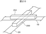
前記有機絶縁膜と前記配向膜と間には、前記コンタクトホールを含む前記映像信号線の延在する方向の断面において、前記コンタクトホールのテーパ部分において、凸部を形成するための物質が積層されていることを特徴とする液晶表示装置。 - 前記凸部を形成するための物質は、前記コンタクトホールにおける前記有機絶縁膜の端部から4乃至10μmの範囲において、前記有機絶縁膜に積層されていることを特徴とする請求項8に記載の液晶表示装置。
- 前記凸部を形成するための物質は、前記コンタクトホールにおける前記有機絶縁膜の端部から3乃至8μmの範囲において、前記有機絶縁膜に積層されていることを特徴とする請求項8に記載の液晶表示装置。
- 前記凸部を形成するための物質の高さは、0.3μm以上、1μm以下であることを特徴とする請求項8に記載の液晶表示装置。
- 前記凸部を形成するための物質は金属によって構成されていることを特徴とする請求項8に記載の液晶表示装置。
- 前記凸部を形成するための物質は有機材料によって構成されていることを特徴とする請求項8に記載の液晶表示装置。
- 第1の方向に延在し、第2の方向に配列した走査線と、第2の方向に延在し、第1の方向に配列した映像信号線の間に画素が形成されたTFT基板と、対向基板の間に液晶が挟持された液晶表示装置であって、
前記画素には、TFTを覆って、有機絶縁膜が形成され、前記有機絶縁膜の上には、第1の電極と、第2の電極が無機絶縁膜を介して対向して形成され、その上に配向膜が形成され、
前記第2の電極と前記TFTは、前記有機絶縁膜に形成されたコンタクトホールを介して接続し、
前記有機絶縁膜の上に形成された前記配向膜の上辺の曲線は、前記コンタクトホールを含む前記第2の方向の断面において、前記有機絶縁膜の前記コンタクトホール内の端部を原点とし、前記TFT基板の平面と平行な方向をxとし、前記配向膜の上辺を示す曲線をf(x)とした場合、
前記f(x)の2次微分の符号が少なくとも1回変化し、
前記符号の変化する範囲は、前記原点から前記x方向において、4乃至10μmの範囲であることを特徴とする液晶表示装置。 - 前記符号の変化する範囲は、前記原点から前記x方向において、3乃至8μmの範囲であることを特徴とする請求項14に記載の液晶表示装置。
- 前記f(x)をax2+bx4で近似した場合に、前記2次微分の符号が少なくとも1回変化することを特徴とする請求項14または15に記載の液晶表示装置。
Priority Applications (4)
| Application Number | Priority Date | Filing Date | Title |
|---|---|---|---|
| JP2016027833A JP6649788B2 (ja) | 2016-02-17 | 2016-02-17 | 液晶表示装置 |
| US15/423,729 US10409112B2 (en) | 2016-02-17 | 2017-02-03 | Liquid crystal display device |
| CN201710078984.9A CN107092113B (zh) | 2016-02-17 | 2017-02-14 | 液晶显示装置 |
| JP2020005662A JP6960002B2 (ja) | 2016-02-17 | 2020-01-17 | 液晶表示装置 |
Applications Claiming Priority (1)
| Application Number | Priority Date | Filing Date | Title |
|---|---|---|---|
| JP2016027833A JP6649788B2 (ja) | 2016-02-17 | 2016-02-17 | 液晶表示装置 |
Related Child Applications (1)
| Application Number | Title | Priority Date | Filing Date |
|---|---|---|---|
| JP2020005662A Division JP6960002B2 (ja) | 2016-02-17 | 2020-01-17 | 液晶表示装置 |
Publications (2)
| Publication Number | Publication Date |
|---|---|
| JP2017146449A true JP2017146449A (ja) | 2017-08-24 |
| JP6649788B2 JP6649788B2 (ja) | 2020-02-19 |
Family
ID=59559615
Family Applications (1)
| Application Number | Title | Priority Date | Filing Date |
|---|---|---|---|
| JP2016027833A Active JP6649788B2 (ja) | 2016-02-17 | 2016-02-17 | 液晶表示装置 |
Country Status (3)
| Country | Link |
|---|---|
| US (1) | US10409112B2 (ja) |
| JP (1) | JP6649788B2 (ja) |
| CN (1) | CN107092113B (ja) |
Cited By (1)
| Publication number | Priority date | Publication date | Assignee | Title |
|---|---|---|---|---|
| JP2020008742A (ja) * | 2018-07-09 | 2020-01-16 | 株式会社ジャパンディスプレイ | 表示装置 |
Families Citing this family (7)
| Publication number | Priority date | Publication date | Assignee | Title |
|---|---|---|---|---|
| CN106444187A (zh) * | 2016-08-22 | 2017-02-22 | 京东方科技集团股份有限公司 | 阵列基板及显示装置 |
| JP2018124480A (ja) * | 2017-02-02 | 2018-08-09 | 株式会社ジャパンディスプレイ | 表示装置 |
| JP2019091346A (ja) * | 2017-11-16 | 2019-06-13 | 株式会社ジャパンディスプレイ | 表示装置 |
| CN109188782B (zh) * | 2018-09-17 | 2020-04-10 | 深圳市华星光电半导体显示技术有限公司 | 液晶显示面板 |
| CN110928016B (zh) * | 2019-12-13 | 2022-02-22 | 武汉华星光电技术有限公司 | 一种显示面板、显示装置及显示装置的制作方法 |
| CN113156714B (zh) * | 2021-04-28 | 2023-12-08 | Tcl华星光电技术有限公司 | 阵列基板及液晶显示面板 |
| CN113589602B (zh) * | 2021-07-20 | 2022-08-23 | Tcl华星光电技术有限公司 | 一种显示面板及显示终端 |
Family Cites Families (18)
| Publication number | Priority date | Publication date | Assignee | Title |
|---|---|---|---|---|
| JP2001194662A (ja) * | 2000-01-14 | 2001-07-19 | Nec Corp | 反射型液晶表示装置及びその製造方法 |
| JP5082172B2 (ja) | 2001-02-05 | 2012-11-28 | ソニー株式会社 | 表示装置の製造方法 |
| JP3951694B2 (ja) | 2001-12-11 | 2007-08-01 | セイコーエプソン株式会社 | 半透過・反射型電気光学装置、電子機器、および半透過・反射型電気光学装置の製造方法 |
| JP2006508032A (ja) * | 2002-05-02 | 2006-03-09 | ワシントン・ユニバーシティ | 糖質コルチコイド調節不全を有する対象におけるt細胞媒介炎症性/自己免疫性疾患および障害を治療するための方法および組成物 |
| KR100913299B1 (ko) * | 2003-03-17 | 2009-08-26 | 삼성전자주식회사 | 어레이 기판과 이를 갖는 반사-투과형 액정 표시 장치 |
| KR100951348B1 (ko) * | 2003-04-04 | 2010-04-08 | 삼성전자주식회사 | 다중 도메인 액정 표시 장치 및 그 박막 트랜지스터 기판 |
| KR100675631B1 (ko) * | 2003-06-27 | 2007-02-01 | 엘지.필립스 엘시디 주식회사 | 횡전계방식 액정표시장치 및 그 제조방법 |
| JP2006098641A (ja) * | 2004-09-29 | 2006-04-13 | Seiko Epson Corp | 薄膜半導体装置、電気光学装置、および電子機器 |
| JP2008268844A (ja) | 2007-03-28 | 2008-11-06 | Epson Imaging Devices Corp | 液晶表示装置および電子機器 |
| JP4799505B2 (ja) * | 2007-08-03 | 2011-10-26 | 株式会社 日立ディスプレイズ | 液晶表示装置 |
| JP2009103775A (ja) * | 2007-10-22 | 2009-05-14 | Hitachi Displays Ltd | 液晶表示装置 |
| US8587754B2 (en) * | 2009-06-30 | 2013-11-19 | Samsung Display Co., Ltd. | Liquid crystal display and method of manufacturing the same |
| EP2275858A1 (en) | 2009-06-30 | 2011-01-19 | Samsung Electronics Co., Ltd. | Liquid crystal display and method of manufacturing the same |
| KR20120015187A (ko) * | 2010-08-11 | 2012-02-21 | 삼성모바일디스플레이주식회사 | 반사형 액정표시장치 |
| CN103430380B (zh) * | 2011-03-16 | 2016-08-03 | 国际商业机器公司 | 具有有效折射率梯度的电磁波谐振器 |
| US20120003887A1 (en) * | 2011-09-21 | 2012-01-05 | Anna Marie Murphy | Floating friendship assembly |
| KR101923717B1 (ko) * | 2012-05-24 | 2018-11-30 | 엘지디스플레이 주식회사 | 액정표시장치 어레이 기판 및 그 제조방법 |
| JP5947650B2 (ja) * | 2012-07-27 | 2016-07-06 | 株式会社ジャパンディスプレイ | 液晶表示装置および電子機器 |
-
2016
- 2016-02-17 JP JP2016027833A patent/JP6649788B2/ja active Active
-
2017
- 2017-02-03 US US15/423,729 patent/US10409112B2/en active Active
- 2017-02-14 CN CN201710078984.9A patent/CN107092113B/zh active Active
Cited By (4)
| Publication number | Priority date | Publication date | Assignee | Title |
|---|---|---|---|---|
| JP2020008742A (ja) * | 2018-07-09 | 2020-01-16 | 株式会社ジャパンディスプレイ | 表示装置 |
| JP7096718B2 (ja) | 2018-07-09 | 2022-07-06 | 株式会社ジャパンディスプレイ | 表示装置 |
| US11391995B2 (en) | 2018-07-09 | 2022-07-19 | Japan Display Inc. | Display device |
| US11762243B2 (en) | 2018-07-09 | 2023-09-19 | Japan Display Inc. | Display device |
Also Published As
| Publication number | Publication date |
|---|---|
| CN107092113B (zh) | 2021-05-14 |
| US20170235167A1 (en) | 2017-08-17 |
| US10409112B2 (en) | 2019-09-10 |
| CN107092113A (zh) | 2017-08-25 |
| JP6649788B2 (ja) | 2020-02-19 |
Similar Documents
| Publication | Publication Date | Title |
|---|---|---|
| JP6649788B2 (ja) | 液晶表示装置 | |
| JP6621284B2 (ja) | 表示装置 | |
| KR102334140B1 (ko) | 표시 장치 및 그 제조 방법 | |
| US11126043B2 (en) | Liquid crystal display device | |
| US10409101B2 (en) | Liquid crystal display device | |
| JP2017146450A (ja) | 表示装置 | |
| US10288942B2 (en) | Liquid crystal display device | |
| JP2015099201A (ja) | 液晶表示装置 | |
| JP2017187530A (ja) | 液晶表示装置 | |
| WO2012124662A1 (ja) | 液晶表示装置 | |
| JP2016015404A (ja) | 液晶表示装置 | |
| JP2016038433A (ja) | 液晶表示装置 | |
| JP6960002B2 (ja) | 液晶表示装置 | |
| JPWO2012124699A1 (ja) | 液晶表示装置 | |
| JP2017122790A (ja) | 液晶表示装置 | |
| JP7183366B2 (ja) | 液晶表示装置 | |
| JP6608014B2 (ja) | 液晶表示装置 | |
| JP2016095336A (ja) | 液晶表示装置 | |
| JP7201777B2 (ja) | 液晶表示装置 | |
| JP6918090B2 (ja) | 液晶表示装置 | |
| JP6980730B2 (ja) | 液晶表示装置 | |
| JP2017122937A (ja) | 液晶表示装置 | |
| JP2015219349A (ja) | 表示装置 |
Legal Events
| Date | Code | Title | Description |
|---|---|---|---|
| A621 | Written request for application examination |
Free format text: JAPANESE INTERMEDIATE CODE: A621 Effective date: 20180906 |
|
| A131 | Notification of reasons for refusal |
Free format text: JAPANESE INTERMEDIATE CODE: A131 Effective date: 20190723 |
|
| A977 | Report on retrieval |
Free format text: JAPANESE INTERMEDIATE CODE: A971007 Effective date: 20190724 |
|
| A521 | Request for written amendment filed |
Free format text: JAPANESE INTERMEDIATE CODE: A523 Effective date: 20190917 |
|
| A131 | Notification of reasons for refusal |
Free format text: JAPANESE INTERMEDIATE CODE: A131 Effective date: 20191015 |
|
| A521 | Request for written amendment filed |
Free format text: JAPANESE INTERMEDIATE CODE: A523 Effective date: 20191209 |
|
| TRDD | Decision of grant or rejection written | ||
| A01 | Written decision to grant a patent or to grant a registration (utility model) |
Free format text: JAPANESE INTERMEDIATE CODE: A01 Effective date: 20191224 |
|
| A61 | First payment of annual fees (during grant procedure) |
Free format text: JAPANESE INTERMEDIATE CODE: A61 Effective date: 20200117 |
|
| R150 | Certificate of patent or registration of utility model |
Ref document number: 6649788 Country of ref document: JP Free format text: JAPANESE INTERMEDIATE CODE: R150 |
|
| R250 | Receipt of annual fees |
Free format text: JAPANESE INTERMEDIATE CODE: R250 |
|
| R250 | Receipt of annual fees |
Free format text: JAPANESE INTERMEDIATE CODE: R250 |