JP2017117944A - 光半導体装置の製造方法 - Google Patents
光半導体装置の製造方法 Download PDFInfo
- Publication number
- JP2017117944A JP2017117944A JP2015252124A JP2015252124A JP2017117944A JP 2017117944 A JP2017117944 A JP 2017117944A JP 2015252124 A JP2015252124 A JP 2015252124A JP 2015252124 A JP2015252124 A JP 2015252124A JP 2017117944 A JP2017117944 A JP 2017117944A
- Authority
- JP
- Japan
- Prior art keywords
- refractive index
- layer
- optical waveguide
- optical semiconductor
- optical
- Prior art date
- Legal status (The legal status is an assumption and is not a legal conclusion. Google has not performed a legal analysis and makes no representation as to the accuracy of the status listed.)
- Granted
Links
- 230000003287 optical effect Effects 0.000 title claims abstract description 166
- 239000004065 semiconductor Substances 0.000 title claims abstract description 105
- 238000004519 manufacturing process Methods 0.000 title claims abstract description 43
- 238000005530 etching Methods 0.000 claims abstract description 22
- 238000005424 photoluminescence Methods 0.000 claims abstract description 14
- 238000007689 inspection Methods 0.000 claims abstract description 11
- 230000005684 electric field Effects 0.000 claims abstract description 3
- 238000005253 cladding Methods 0.000 claims description 16
- 239000000758 substrate Substances 0.000 claims description 14
- 238000010030 laminating Methods 0.000 claims description 5
- 239000000203 mixture Substances 0.000 description 16
- 229910004298 SiO 2 Inorganic materials 0.000 description 12
- 238000000034 method Methods 0.000 description 11
- 239000000463 material Substances 0.000 description 10
- 239000011259 mixed solution Substances 0.000 description 7
- VEXZGXHMUGYJMC-UHFFFAOYSA-N Hydrochloric acid Chemical compound Cl VEXZGXHMUGYJMC-UHFFFAOYSA-N 0.000 description 6
- NBIIXXVUZAFLBC-UHFFFAOYSA-N Phosphoric acid Chemical compound OP(O)(O)=O NBIIXXVUZAFLBC-UHFFFAOYSA-N 0.000 description 6
- FEWJPZIEWOKRBE-JCYAYHJZSA-N Dextrotartaric acid Chemical compound OC(=O)[C@H](O)[C@@H](O)C(O)=O FEWJPZIEWOKRBE-JCYAYHJZSA-N 0.000 description 5
- MHAJPDPJQMAIIY-UHFFFAOYSA-N Hydrogen peroxide Chemical compound OO MHAJPDPJQMAIIY-UHFFFAOYSA-N 0.000 description 5
- FEWJPZIEWOKRBE-UHFFFAOYSA-N Tartaric acid Natural products [H+].[H+].[O-]C(=O)C(O)C(O)C([O-])=O FEWJPZIEWOKRBE-UHFFFAOYSA-N 0.000 description 5
- 230000000694 effects Effects 0.000 description 5
- 235000002906 tartaric acid Nutrition 0.000 description 5
- 239000011975 tartaric acid Substances 0.000 description 5
- 238000001039 wet etching Methods 0.000 description 5
- KRHYYFGTRYWZRS-UHFFFAOYSA-N Fluorane Chemical compound F KRHYYFGTRYWZRS-UHFFFAOYSA-N 0.000 description 4
- 238000004364 calculation method Methods 0.000 description 4
- 238000001312 dry etching Methods 0.000 description 4
- 229910000147 aluminium phosphate Inorganic materials 0.000 description 3
- 238000010586 diagram Methods 0.000 description 3
- 238000009826 distribution Methods 0.000 description 3
- 238000002347 injection Methods 0.000 description 3
- 239000007924 injection Substances 0.000 description 3
- 238000002488 metal-organic chemical vapour deposition Methods 0.000 description 3
- 238000010521 absorption reaction Methods 0.000 description 2
- 239000013078 crystal Substances 0.000 description 2
- QOSATHPSBFQAML-UHFFFAOYSA-N hydrogen peroxide;hydrate Chemical compound O.OO QOSATHPSBFQAML-UHFFFAOYSA-N 0.000 description 2
- 238000012986 modification Methods 0.000 description 2
- 230000004048 modification Effects 0.000 description 2
- 229910052782 aluminium Inorganic materials 0.000 description 1
- 230000015572 biosynthetic process Effects 0.000 description 1
- 230000015556 catabolic process Effects 0.000 description 1
- 238000004891 communication Methods 0.000 description 1
- 238000012937 correction Methods 0.000 description 1
- 230000003247 decreasing effect Effects 0.000 description 1
- 238000006731 degradation reaction Methods 0.000 description 1
- 238000005516 engineering process Methods 0.000 description 1
- 229910052733 gallium Inorganic materials 0.000 description 1
- 229910052738 indium Inorganic materials 0.000 description 1
- 230000005693 optoelectronics Effects 0.000 description 1
- 150000007524 organic acids Chemical class 0.000 description 1
- 230000001902 propagating effect Effects 0.000 description 1
- 238000003892 spreading Methods 0.000 description 1
- 238000012360 testing method Methods 0.000 description 1
- 238000007740 vapor deposition Methods 0.000 description 1
Images


Classifications
-
- H—ELECTRICITY
- H01—ELECTRIC ELEMENTS
- H01S—DEVICES USING THE PROCESS OF LIGHT AMPLIFICATION BY STIMULATED EMISSION OF RADIATION [LASER] TO AMPLIFY OR GENERATE LIGHT; DEVICES USING STIMULATED EMISSION OF ELECTROMAGNETIC RADIATION IN WAVE RANGES OTHER THAN OPTICAL
- H01S5/00—Semiconductor lasers
- H01S5/30—Structure or shape of the active region; Materials used for the active region
- H01S5/32—Structure or shape of the active region; Materials used for the active region comprising PN junctions, e.g. hetero- or double- heterostructures
- H01S5/323—Structure or shape of the active region; Materials used for the active region comprising PN junctions, e.g. hetero- or double- heterostructures in AIIIBV compounds, e.g. AlGaAs-laser, InP-based laser
- H01S5/32308—Structure or shape of the active region; Materials used for the active region comprising PN junctions, e.g. hetero- or double- heterostructures in AIIIBV compounds, e.g. AlGaAs-laser, InP-based laser emitting light at a wavelength less than 900 nm
-
- H—ELECTRICITY
- H01—ELECTRIC ELEMENTS
- H01S—DEVICES USING THE PROCESS OF LIGHT AMPLIFICATION BY STIMULATED EMISSION OF RADIATION [LASER] TO AMPLIFY OR GENERATE LIGHT; DEVICES USING STIMULATED EMISSION OF ELECTROMAGNETIC RADIATION IN WAVE RANGES OTHER THAN OPTICAL
- H01S5/00—Semiconductor lasers
- H01S5/20—Structure or shape of the semiconductor body to guide the optical wave ; Confining structures perpendicular to the optical axis, e.g. index or gain guiding, stripe geometry, broad area lasers, gain tailoring, transverse or lateral reflectors, special cladding structures, MQW barrier reflection layers
- H01S5/22—Structure or shape of the semiconductor body to guide the optical wave ; Confining structures perpendicular to the optical axis, e.g. index or gain guiding, stripe geometry, broad area lasers, gain tailoring, transverse or lateral reflectors, special cladding structures, MQW barrier reflection layers having a ridge or stripe structure
- H01S5/227—Buried mesa structure ; Striped active layer
- H01S5/2275—Buried mesa structure ; Striped active layer mesa created by etching
-
- H—ELECTRICITY
- H01—ELECTRIC ELEMENTS
- H01L—SEMICONDUCTOR DEVICES NOT COVERED BY CLASS H10
- H01L33/00—Semiconductor devices with at least one potential-jump barrier or surface barrier specially adapted for light emission; Processes or apparatus specially adapted for the manufacture or treatment thereof or of parts thereof; Details thereof
- H01L33/005—Processes
- H01L33/0062—Processes for devices with an active region comprising only III-V compounds
- H01L33/0066—Processes for devices with an active region comprising only III-V compounds with a substrate not being a III-V compound
-
- H—ELECTRICITY
- H01—ELECTRIC ELEMENTS
- H01L—SEMICONDUCTOR DEVICES NOT COVERED BY CLASS H10
- H01L33/00—Semiconductor devices with at least one potential-jump barrier or surface barrier specially adapted for light emission; Processes or apparatus specially adapted for the manufacture or treatment thereof or of parts thereof; Details thereof
- H01L33/02—Semiconductor devices with at least one potential-jump barrier or surface barrier specially adapted for light emission; Processes or apparatus specially adapted for the manufacture or treatment thereof or of parts thereof; Details thereof characterised by the semiconductor bodies
- H01L33/10—Semiconductor devices with at least one potential-jump barrier or surface barrier specially adapted for light emission; Processes or apparatus specially adapted for the manufacture or treatment thereof or of parts thereof; Details thereof characterised by the semiconductor bodies with a light reflecting structure, e.g. semiconductor Bragg reflector
-
- H—ELECTRICITY
- H01—ELECTRIC ELEMENTS
- H01L—SEMICONDUCTOR DEVICES NOT COVERED BY CLASS H10
- H01L33/00—Semiconductor devices with at least one potential-jump barrier or surface barrier specially adapted for light emission; Processes or apparatus specially adapted for the manufacture or treatment thereof or of parts thereof; Details thereof
- H01L33/02—Semiconductor devices with at least one potential-jump barrier or surface barrier specially adapted for light emission; Processes or apparatus specially adapted for the manufacture or treatment thereof or of parts thereof; Details thereof characterised by the semiconductor bodies
- H01L33/14—Semiconductor devices with at least one potential-jump barrier or surface barrier specially adapted for light emission; Processes or apparatus specially adapted for the manufacture or treatment thereof or of parts thereof; Details thereof characterised by the semiconductor bodies with a carrier transport control structure, e.g. highly-doped semiconductor layer or current-blocking structure
- H01L33/145—Semiconductor devices with at least one potential-jump barrier or surface barrier specially adapted for light emission; Processes or apparatus specially adapted for the manufacture or treatment thereof or of parts thereof; Details thereof characterised by the semiconductor bodies with a carrier transport control structure, e.g. highly-doped semiconductor layer or current-blocking structure with a current-blocking structure
-
- H—ELECTRICITY
- H01—ELECTRIC ELEMENTS
- H01L—SEMICONDUCTOR DEVICES NOT COVERED BY CLASS H10
- H01L33/00—Semiconductor devices with at least one potential-jump barrier or surface barrier specially adapted for light emission; Processes or apparatus specially adapted for the manufacture or treatment thereof or of parts thereof; Details thereof
- H01L33/48—Semiconductor devices with at least one potential-jump barrier or surface barrier specially adapted for light emission; Processes or apparatus specially adapted for the manufacture or treatment thereof or of parts thereof; Details thereof characterised by the semiconductor body packages
- H01L33/58—Optical field-shaping elements
- H01L33/60—Reflective elements
-
- H—ELECTRICITY
- H01—ELECTRIC ELEMENTS
- H01S—DEVICES USING THE PROCESS OF LIGHT AMPLIFICATION BY STIMULATED EMISSION OF RADIATION [LASER] TO AMPLIFY OR GENERATE LIGHT; DEVICES USING STIMULATED EMISSION OF ELECTROMAGNETIC RADIATION IN WAVE RANGES OTHER THAN OPTICAL
- H01S5/00—Semiconductor lasers
- H01S5/02—Structural details or components not essential to laser action
- H01S5/026—Monolithically integrated components, e.g. waveguides, monitoring photo-detectors, drivers
-
- H—ELECTRICITY
- H01—ELECTRIC ELEMENTS
- H01S—DEVICES USING THE PROCESS OF LIGHT AMPLIFICATION BY STIMULATED EMISSION OF RADIATION [LASER] TO AMPLIFY OR GENERATE LIGHT; DEVICES USING STIMULATED EMISSION OF ELECTROMAGNETIC RADIATION IN WAVE RANGES OTHER THAN OPTICAL
- H01S5/00—Semiconductor lasers
- H01S5/30—Structure or shape of the active region; Materials used for the active region
- H01S5/32—Structure or shape of the active region; Materials used for the active region comprising PN junctions, e.g. hetero- or double- heterostructures
- H01S5/323—Structure or shape of the active region; Materials used for the active region comprising PN junctions, e.g. hetero- or double- heterostructures in AIIIBV compounds, e.g. AlGaAs-laser, InP-based laser
- H01S5/32308—Structure or shape of the active region; Materials used for the active region comprising PN junctions, e.g. hetero- or double- heterostructures in AIIIBV compounds, e.g. AlGaAs-laser, InP-based laser emitting light at a wavelength less than 900 nm
- H01S5/32333—Structure or shape of the active region; Materials used for the active region comprising PN junctions, e.g. hetero- or double- heterostructures in AIIIBV compounds, e.g. AlGaAs-laser, InP-based laser emitting light at a wavelength less than 900 nm based on InGaAsP
-
- H—ELECTRICITY
- H01—ELECTRIC ELEMENTS
- H01L—SEMICONDUCTOR DEVICES NOT COVERED BY CLASS H10
- H01L33/00—Semiconductor devices with at least one potential-jump barrier or surface barrier specially adapted for light emission; Processes or apparatus specially adapted for the manufacture or treatment thereof or of parts thereof; Details thereof
- H01L33/005—Processes
-
- H—ELECTRICITY
- H01—ELECTRIC ELEMENTS
- H01S—DEVICES USING THE PROCESS OF LIGHT AMPLIFICATION BY STIMULATED EMISSION OF RADIATION [LASER] TO AMPLIFY OR GENERATE LIGHT; DEVICES USING STIMULATED EMISSION OF ELECTROMAGNETIC RADIATION IN WAVE RANGES OTHER THAN OPTICAL
- H01S2304/00—Special growth methods for semiconductor lasers
- H01S2304/04—MOCVD or MOVPE
-
- H—ELECTRICITY
- H01—ELECTRIC ELEMENTS
- H01S—DEVICES USING THE PROCESS OF LIGHT AMPLIFICATION BY STIMULATED EMISSION OF RADIATION [LASER] TO AMPLIFY OR GENERATE LIGHT; DEVICES USING STIMULATED EMISSION OF ELECTROMAGNETIC RADIATION IN WAVE RANGES OTHER THAN OPTICAL
- H01S5/00—Semiconductor lasers
- H01S5/20—Structure or shape of the semiconductor body to guide the optical wave ; Confining structures perpendicular to the optical axis, e.g. index or gain guiding, stripe geometry, broad area lasers, gain tailoring, transverse or lateral reflectors, special cladding structures, MQW barrier reflection layers
- H01S5/22—Structure or shape of the semiconductor body to guide the optical wave ; Confining structures perpendicular to the optical axis, e.g. index or gain guiding, stripe geometry, broad area lasers, gain tailoring, transverse or lateral reflectors, special cladding structures, MQW barrier reflection layers having a ridge or stripe structure
- H01S5/2205—Structure or shape of the semiconductor body to guide the optical wave ; Confining structures perpendicular to the optical axis, e.g. index or gain guiding, stripe geometry, broad area lasers, gain tailoring, transverse or lateral reflectors, special cladding structures, MQW barrier reflection layers having a ridge or stripe structure comprising special burying or current confinement layers
- H01S5/2222—Structure or shape of the semiconductor body to guide the optical wave ; Confining structures perpendicular to the optical axis, e.g. index or gain guiding, stripe geometry, broad area lasers, gain tailoring, transverse or lateral reflectors, special cladding structures, MQW barrier reflection layers having a ridge or stripe structure comprising special burying or current confinement layers having special electric properties
- H01S5/2224—Structure or shape of the semiconductor body to guide the optical wave ; Confining structures perpendicular to the optical axis, e.g. index or gain guiding, stripe geometry, broad area lasers, gain tailoring, transverse or lateral reflectors, special cladding structures, MQW barrier reflection layers having a ridge or stripe structure comprising special burying or current confinement layers having special electric properties semi-insulating semiconductors
Abstract
Description
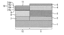
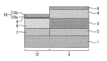
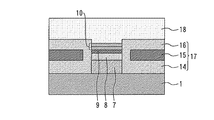
図1は、本発明の実施の形態1に係る光半導体装置の製造方法のフローチャートである。図2から図15は、本発明の実施の形態1に係る光半導体装置の製造方法を示す断面図である。ただし、図2〜9,13は共振器方向に沿った断面図であり、図10〜12,14は共振器方向に垂直な断面図である。図16は、本発明の実施の形態1に係る光半導体装置を示す斜視図である。図17は、本発明の実施の形態1に係る光半導体装置の内部を透視した斜視図である。これらの図を参照しながら本実施の形態に係る光半導体装置の製造方法を説明する。
図21は、本発明の実施の形態2に係る光半導体装置の製造方法を示す断面図である。実施の形態1では光半導体素子5の屈折率分布中心に対して光導波路12の屈折率分布中心が偏心している。これを補正するため、本実施の形態では光導波路層8の膜厚を活性層3の膜厚よりも薄くして、光半導体素子5の屈折率分布中心に対して光導波路12の屈折率分布中心が偏心しないようにする。なお、活性層3にAlGaInAs材料を使用し、屈折率調整層10をエッチングする際に活性層3がエッチングされないようにする。その他の構成及び効果は実施の形態1と同様である。
図22〜24は、本発明の実施の形態3に係る光半導体装置の製造方法を示す断面図である。
図25は、本発明の実施の形態4に係る光半導体装置の製造方法を示す断面図である。実施の形態3では光半導体素子5の屈折率分布中心に対して光導波路12の屈折率分布中心が偏心している。これを補正するため、本実施の形態では光導波路層8の膜厚を活性層3の膜厚よりも薄くして、光半導体素子5の屈折率分布中心に対して光導波路12の屈折率分布中心が偏心しないようにする。なお、活性層3にAlGaInAs材料を使用し、屈折率調整層21をエッチングする際に活性層3がエッチングされないようにする。その他の構成及び効果は実施の形態3と同様である。
Claims (5)
- 半導体基板上に第1のクラッド層、活性層、及び第2のクラッド層を順に積層して光半導体素子を形成する工程と、
フォトルミネセンス検査により前記活性層の屈折率を求めて前記光半導体素子の等価屈折率を算出する工程と、
前記半導体基板上に第3のクラッド層、前記活性層に接合され前記活性層の屈折率よりも小さい屈折率を有する光導波路層、及び屈折率調整層を順に積層して光導波路を形成する工程と、
フォトルミネセンス検査により前記光導波路層の屈折率を求めて前記光導波路の等価屈折率を算出する工程と、
前記屈折率調整層をエッチングして、前記光半導体素子の等価屈折率と前記光導波路の等価屈折率が整合するように前記屈折率調整層の膜厚を調整する工程と、
前記屈折率調整層の膜厚を調整した後に、前記第2のクラッド層及び前記屈折率調整層上にコンタクト層を形成する工程とを備え、
前記光導波路は、電界が印加されず電流が注入されないパッシブ導波路であることを特徴とする光半導体装置の製造方法。 - 前記屈折率調整層は、前記光導波路層から遠ざかるほど低屈折率となる積層された複数の半導体層を有することを特徴とする請求項1に記載の光半導体装置の製造方法。
- 前記屈折率調整層は、異なる2種類の半導体層を交互に積層したものであることを特徴とする請求項1に記載の光半導体装置の製造方法。
- 前記光導波路層の膜厚を前記活性層の膜厚よりも薄くして、前記光半導体素子の屈折率分布中心に対して前記光導波路の屈折率分布中心が偏心しないようにすることを特徴とする請求項1〜3の何れか1項に記載の光半導体装置の製造方法。
- 前記屈折率調整層をエッチングする際に前記活性層がエッチングされないようにすることを特徴とする請求項4に記載の光半導体装置の製造方法。
Priority Applications (2)
| Application Number | Priority Date | Filing Date | Title |
|---|---|---|---|
| JP2015252124A JP6468180B2 (ja) | 2015-12-24 | 2015-12-24 | 光半導体装置の製造方法 |
| US15/246,744 US9647425B1 (en) | 2015-12-24 | 2016-08-25 | Method of manufacturing optical semiconductor device |
Applications Claiming Priority (1)
| Application Number | Priority Date | Filing Date | Title |
|---|---|---|---|
| JP2015252124A JP6468180B2 (ja) | 2015-12-24 | 2015-12-24 | 光半導体装置の製造方法 |
Publications (2)
| Publication Number | Publication Date |
|---|---|
| JP2017117944A true JP2017117944A (ja) | 2017-06-29 |
| JP6468180B2 JP6468180B2 (ja) | 2019-02-13 |
Family
ID=58643576
Family Applications (1)
| Application Number | Title | Priority Date | Filing Date |
|---|---|---|---|
| JP2015252124A Active JP6468180B2 (ja) | 2015-12-24 | 2015-12-24 | 光半導体装置の製造方法 |
Country Status (2)
| Country | Link |
|---|---|
| US (1) | US9647425B1 (ja) |
| JP (1) | JP6468180B2 (ja) |
Families Citing this family (2)
| Publication number | Priority date | Publication date | Assignee | Title |
|---|---|---|---|---|
| US10784649B2 (en) * | 2017-03-23 | 2020-09-22 | Mitsubishi Electric Corporation | Optical semiconductor device |
| GB2602963A (en) * | 2020-12-31 | 2022-07-27 | Smart Photonics Holding B V | Semiconductor structure for photonic integrated circuit and method of manufacture |
Citations (5)
| Publication number | Priority date | Publication date | Assignee | Title |
|---|---|---|---|---|
| JPH09246667A (ja) * | 1996-03-12 | 1997-09-19 | Yokogawa Electric Corp | 半導体レーザおよびその製造方法 |
| JP2006222305A (ja) * | 2005-02-10 | 2006-08-24 | Nippon Telegr & Teleph Corp <Ntt> | 半導体光素子およびその波長調整方法 |
| JP2006269759A (ja) * | 2005-03-24 | 2006-10-05 | Sharp Corp | 窓構造半導体レーザ装置およびその製造方法 |
| WO2007096939A1 (ja) * | 2006-02-20 | 2007-08-30 | Fujitsu Limited | 光半導体装置とその製造方法 |
| US20150236473A1 (en) * | 2014-02-17 | 2015-08-20 | Electronics And Telecommunications Research Institute | Reflective optical source device |
Family Cites Families (14)
| Publication number | Priority date | Publication date | Assignee | Title |
|---|---|---|---|---|
| JP2000277869A (ja) * | 1999-03-29 | 2000-10-06 | Mitsubishi Electric Corp | 変調器集積型半導体レーザ装置及びその製造方法 |
| US6528337B1 (en) * | 1999-04-08 | 2003-03-04 | The Furukawa Electric Co., Ltd. | Process of producing semiconductor layer structure |
| JP2004273993A (ja) * | 2003-03-12 | 2004-09-30 | Hitachi Ltd | 波長可変分布反射型半導体レーザ装置 |
| JP4952376B2 (ja) * | 2006-08-10 | 2012-06-13 | 三菱電機株式会社 | 光導波路と半導体光集積素子の製造方法 |
| JP4930925B2 (ja) * | 2008-01-11 | 2012-05-16 | パナソニック株式会社 | 二波長半導体レーザ装置 |
| JP2013149724A (ja) * | 2012-01-18 | 2013-08-01 | Sumitomo Electric Ind Ltd | 光集積素子の製造方法 |
| JP5880065B2 (ja) * | 2012-01-18 | 2016-03-08 | 住友電気工業株式会社 | 光集積素子の製造方法 |
| JP5880063B2 (ja) * | 2012-01-18 | 2016-03-08 | 住友電気工業株式会社 | 光集積素子の製造方法 |
| JP2014053346A (ja) * | 2012-09-05 | 2014-03-20 | Seiko Epson Corp | 短光パルス発生装置、テラヘルツ波発生装置、カメラ、イメージング装置、および計測装置 |
| JP6084428B2 (ja) | 2012-10-18 | 2017-02-22 | 日本オクラロ株式会社 | 半導体光集積素子及びその製造方法 |
| WO2015038164A1 (en) * | 2013-09-16 | 2015-03-19 | Intel Corporation | Hybrid optical apparatuses including optical waveguides |
| US9077144B2 (en) * | 2013-09-30 | 2015-07-07 | Jds Uniphase Corporation | MOPA laser source with wavelength control |
| JP6291849B2 (ja) * | 2014-01-10 | 2018-03-14 | 三菱電機株式会社 | 半導体装置の製造方法、半導体装置 |
| JP6331997B2 (ja) * | 2014-11-28 | 2018-05-30 | 三菱電機株式会社 | 半導体光素子 |
-
2015
- 2015-12-24 JP JP2015252124A patent/JP6468180B2/ja active Active
-
2016
- 2016-08-25 US US15/246,744 patent/US9647425B1/en active Active
Patent Citations (5)
| Publication number | Priority date | Publication date | Assignee | Title |
|---|---|---|---|---|
| JPH09246667A (ja) * | 1996-03-12 | 1997-09-19 | Yokogawa Electric Corp | 半導体レーザおよびその製造方法 |
| JP2006222305A (ja) * | 2005-02-10 | 2006-08-24 | Nippon Telegr & Teleph Corp <Ntt> | 半導体光素子およびその波長調整方法 |
| JP2006269759A (ja) * | 2005-03-24 | 2006-10-05 | Sharp Corp | 窓構造半導体レーザ装置およびその製造方法 |
| WO2007096939A1 (ja) * | 2006-02-20 | 2007-08-30 | Fujitsu Limited | 光半導体装置とその製造方法 |
| US20150236473A1 (en) * | 2014-02-17 | 2015-08-20 | Electronics And Telecommunications Research Institute | Reflective optical source device |
Also Published As
| Publication number | Publication date |
|---|---|
| JP6468180B2 (ja) | 2019-02-13 |
| US9647425B1 (en) | 2017-05-09 |
Similar Documents
| Publication | Publication Date | Title |
|---|---|---|
| JP5177285B2 (ja) | 光素子及びその製造方法 | |
| KR102163734B1 (ko) | 실리콘 기판 상에 반도체 광증폭기와 통합 형성된 양자점 레이저 소자 | |
| JP5182362B2 (ja) | 光素子及びその製造方法 | |
| JP2010251609A (ja) | 半導体レーザ | |
| JP2011204895A (ja) | 半導体レーザ装置 | |
| CN112290382B (zh) | 一种半导体激光器及其制作方法 | |
| US9793093B2 (en) | System for manufacturing semiconductor device | |
| JP6468180B2 (ja) | 光半導体装置の製造方法 | |
| US9912122B2 (en) | Semiconductor optical device | |
| JP2016096310A (ja) | 半導体光素子およびその製造方法 | |
| CN109449756B (zh) | 一种半导体激光器及其制备方法 | |
| CN107623250B (zh) | 一种短腔长面发射激光器及其制造方法 | |
| WO2018105015A1 (ja) | 半導体レーザの製造方法 | |
| US20030017662A1 (en) | High power single mode laser and method of fabrication | |
| JP4984514B2 (ja) | 半導体発光素子および該半導体発光素子の製造方法 | |
| JP6657537B2 (ja) | 半導体レーザ素子及び半導体レーザ素子の製造方法 | |
| CN110178275B (zh) | 半导体激光元件、半导体激光元件的制造方法 | |
| JP2003234540A (ja) | 分布帰還型レーザ装置、半導体光装置および分布帰還型レーザ装置の製造方法 | |
| JP2010123726A (ja) | 半導体レーザおよびその製造方法 | |
| JP2015056509A (ja) | 半導体光共振器、半導体光素子及び光通信モジュール | |
| JP2013025208A (ja) | 半導体光素子及び半導体光素子の製造方法 | |
| JP2016184705A (ja) | 半導体光素子およびその製造方法 | |
| JP2947702B2 (ja) | 波長可変レーザ装置およびその作製方法 | |
| KR102227495B1 (ko) | 레이저 다이오드 소자 및 이의 제조 방법 | |
| JP2013105958A (ja) | 光半導体装置及びその製造方法 |
Legal Events
| Date | Code | Title | Description |
|---|---|---|---|
| A621 | Written request for application examination |
Free format text: JAPANESE INTERMEDIATE CODE: A621 Effective date: 20180202 |
|
| A977 | Report on retrieval |
Free format text: JAPANESE INTERMEDIATE CODE: A971007 Effective date: 20181115 |
|
| TRDD | Decision of grant or rejection written | ||
| A01 | Written decision to grant a patent or to grant a registration (utility model) |
Free format text: JAPANESE INTERMEDIATE CODE: A01 Effective date: 20181218 |
|
| A61 | First payment of annual fees (during grant procedure) |
Free format text: JAPANESE INTERMEDIATE CODE: A61 Effective date: 20181231 |
|
| R150 | Certificate of patent or registration of utility model |
Ref document number: 6468180 Country of ref document: JP Free format text: JAPANESE INTERMEDIATE CODE: R150 |
|
| R250 | Receipt of annual fees |
Free format text: JAPANESE INTERMEDIATE CODE: R250 |
|
| R250 | Receipt of annual fees |
Free format text: JAPANESE INTERMEDIATE CODE: R250 |
|
| R250 | Receipt of annual fees |
Free format text: JAPANESE INTERMEDIATE CODE: R250 |