JP2017106962A - 表示装置 - Google Patents
表示装置 Download PDFInfo
- Publication number
- JP2017106962A JP2017106962A JP2015238496A JP2015238496A JP2017106962A JP 2017106962 A JP2017106962 A JP 2017106962A JP 2015238496 A JP2015238496 A JP 2015238496A JP 2015238496 A JP2015238496 A JP 2015238496A JP 2017106962 A JP2017106962 A JP 2017106962A
- Authority
- JP
- Japan
- Prior art keywords
- light
- light modulation
- display
- display device
- electrode
- Prior art date
- Legal status (The legal status is an assumption and is not a legal conclusion. Google has not performed a legal analysis and makes no representation as to the accuracy of the status listed.)
- Granted
Links
Images


Classifications
-
- G—PHYSICS
- G02—OPTICS
- G02F—OPTICAL DEVICES OR ARRANGEMENTS FOR THE CONTROL OF LIGHT BY MODIFICATION OF THE OPTICAL PROPERTIES OF THE MEDIA OF THE ELEMENTS INVOLVED THEREIN; NON-LINEAR OPTICS; FREQUENCY-CHANGING OF LIGHT; OPTICAL LOGIC ELEMENTS; OPTICAL ANALOGUE/DIGITAL CONVERTERS
- G02F1/00—Devices or arrangements for the control of the intensity, colour, phase, polarisation or direction of light arriving from an independent light source, e.g. switching, gating or modulating; Non-linear optics
- G02F1/01—Devices or arrangements for the control of the intensity, colour, phase, polarisation or direction of light arriving from an independent light source, e.g. switching, gating or modulating; Non-linear optics for the control of the intensity, phase, polarisation or colour
- G02F1/13—Devices or arrangements for the control of the intensity, colour, phase, polarisation or direction of light arriving from an independent light source, e.g. switching, gating or modulating; Non-linear optics for the control of the intensity, phase, polarisation or colour based on liquid crystals, e.g. single liquid crystal display cells
- G02F1/133—Constructional arrangements; Operation of liquid crystal cells; Circuit arrangements
- G02F1/1333—Constructional arrangements; Manufacturing methods
- G02F1/1335—Structural association of cells with optical devices, e.g. polarisers or reflectors
- G02F1/1336—Illuminating devices
- G02F1/133615—Edge-illuminating devices, i.e. illuminating from the side
-
- G—PHYSICS
- G02—OPTICS
- G02F—OPTICAL DEVICES OR ARRANGEMENTS FOR THE CONTROL OF LIGHT BY MODIFICATION OF THE OPTICAL PROPERTIES OF THE MEDIA OF THE ELEMENTS INVOLVED THEREIN; NON-LINEAR OPTICS; FREQUENCY-CHANGING OF LIGHT; OPTICAL LOGIC ELEMENTS; OPTICAL ANALOGUE/DIGITAL CONVERTERS
- G02F1/00—Devices or arrangements for the control of the intensity, colour, phase, polarisation or direction of light arriving from an independent light source, e.g. switching, gating or modulating; Non-linear optics
- G02F1/01—Devices or arrangements for the control of the intensity, colour, phase, polarisation or direction of light arriving from an independent light source, e.g. switching, gating or modulating; Non-linear optics for the control of the intensity, phase, polarisation or colour
- G02F1/13—Devices or arrangements for the control of the intensity, colour, phase, polarisation or direction of light arriving from an independent light source, e.g. switching, gating or modulating; Non-linear optics for the control of the intensity, phase, polarisation or colour based on liquid crystals, e.g. single liquid crystal display cells
- G02F1/133—Constructional arrangements; Operation of liquid crystal cells; Circuit arrangements
- G02F1/1333—Constructional arrangements; Manufacturing methods
- G02F1/1334—Constructional arrangements; Manufacturing methods based on polymer dispersed liquid crystals, e.g. microencapsulated liquid crystals
-
- G—PHYSICS
- G02—OPTICS
- G02F—OPTICAL DEVICES OR ARRANGEMENTS FOR THE CONTROL OF LIGHT BY MODIFICATION OF THE OPTICAL PROPERTIES OF THE MEDIA OF THE ELEMENTS INVOLVED THEREIN; NON-LINEAR OPTICS; FREQUENCY-CHANGING OF LIGHT; OPTICAL LOGIC ELEMENTS; OPTICAL ANALOGUE/DIGITAL CONVERTERS
- G02F1/00—Devices or arrangements for the control of the intensity, colour, phase, polarisation or direction of light arriving from an independent light source, e.g. switching, gating or modulating; Non-linear optics
- G02F1/01—Devices or arrangements for the control of the intensity, colour, phase, polarisation or direction of light arriving from an independent light source, e.g. switching, gating or modulating; Non-linear optics for the control of the intensity, phase, polarisation or colour
- G02F1/13—Devices or arrangements for the control of the intensity, colour, phase, polarisation or direction of light arriving from an independent light source, e.g. switching, gating or modulating; Non-linear optics for the control of the intensity, phase, polarisation or colour based on liquid crystals, e.g. single liquid crystal display cells
- G02F1/133—Constructional arrangements; Operation of liquid crystal cells; Circuit arrangements
- G02F1/1333—Constructional arrangements; Manufacturing methods
- G02F1/1335—Structural association of cells with optical devices, e.g. polarisers or reflectors
- G02F1/133509—Filters, e.g. light shielding masks
-
- G—PHYSICS
- G02—OPTICS
- G02F—OPTICAL DEVICES OR ARRANGEMENTS FOR THE CONTROL OF LIGHT BY MODIFICATION OF THE OPTICAL PROPERTIES OF THE MEDIA OF THE ELEMENTS INVOLVED THEREIN; NON-LINEAR OPTICS; FREQUENCY-CHANGING OF LIGHT; OPTICAL LOGIC ELEMENTS; OPTICAL ANALOGUE/DIGITAL CONVERTERS
- G02F1/00—Devices or arrangements for the control of the intensity, colour, phase, polarisation or direction of light arriving from an independent light source, e.g. switching, gating or modulating; Non-linear optics
- G02F1/01—Devices or arrangements for the control of the intensity, colour, phase, polarisation or direction of light arriving from an independent light source, e.g. switching, gating or modulating; Non-linear optics for the control of the intensity, phase, polarisation or colour
- G02F1/13—Devices or arrangements for the control of the intensity, colour, phase, polarisation or direction of light arriving from an independent light source, e.g. switching, gating or modulating; Non-linear optics for the control of the intensity, phase, polarisation or colour based on liquid crystals, e.g. single liquid crystal display cells
- G02F1/133—Constructional arrangements; Operation of liquid crystal cells; Circuit arrangements
- G02F1/1333—Constructional arrangements; Manufacturing methods
- G02F1/1335—Structural association of cells with optical devices, e.g. polarisers or reflectors
- G02F1/133553—Reflecting elements
-
- G—PHYSICS
- G02—OPTICS
- G02F—OPTICAL DEVICES OR ARRANGEMENTS FOR THE CONTROL OF LIGHT BY MODIFICATION OF THE OPTICAL PROPERTIES OF THE MEDIA OF THE ELEMENTS INVOLVED THEREIN; NON-LINEAR OPTICS; FREQUENCY-CHANGING OF LIGHT; OPTICAL LOGIC ELEMENTS; OPTICAL ANALOGUE/DIGITAL CONVERTERS
- G02F1/00—Devices or arrangements for the control of the intensity, colour, phase, polarisation or direction of light arriving from an independent light source, e.g. switching, gating or modulating; Non-linear optics
- G02F1/01—Devices or arrangements for the control of the intensity, colour, phase, polarisation or direction of light arriving from an independent light source, e.g. switching, gating or modulating; Non-linear optics for the control of the intensity, phase, polarisation or colour
- G02F1/13—Devices or arrangements for the control of the intensity, colour, phase, polarisation or direction of light arriving from an independent light source, e.g. switching, gating or modulating; Non-linear optics for the control of the intensity, phase, polarisation or colour based on liquid crystals, e.g. single liquid crystal display cells
- G02F1/133—Constructional arrangements; Operation of liquid crystal cells; Circuit arrangements
- G02F1/1333—Constructional arrangements; Manufacturing methods
- G02F1/1337—Surface-induced orientation of the liquid crystal molecules, e.g. by alignment layers
-
- G—PHYSICS
- G02—OPTICS
- G02F—OPTICAL DEVICES OR ARRANGEMENTS FOR THE CONTROL OF LIGHT BY MODIFICATION OF THE OPTICAL PROPERTIES OF THE MEDIA OF THE ELEMENTS INVOLVED THEREIN; NON-LINEAR OPTICS; FREQUENCY-CHANGING OF LIGHT; OPTICAL LOGIC ELEMENTS; OPTICAL ANALOGUE/DIGITAL CONVERTERS
- G02F1/00—Devices or arrangements for the control of the intensity, colour, phase, polarisation or direction of light arriving from an independent light source, e.g. switching, gating or modulating; Non-linear optics
- G02F1/01—Devices or arrangements for the control of the intensity, colour, phase, polarisation or direction of light arriving from an independent light source, e.g. switching, gating or modulating; Non-linear optics for the control of the intensity, phase, polarisation or colour
- G02F1/13—Devices or arrangements for the control of the intensity, colour, phase, polarisation or direction of light arriving from an independent light source, e.g. switching, gating or modulating; Non-linear optics for the control of the intensity, phase, polarisation or colour based on liquid crystals, e.g. single liquid crystal display cells
- G02F1/133—Constructional arrangements; Operation of liquid crystal cells; Circuit arrangements
- G02F1/1333—Constructional arrangements; Manufacturing methods
- G02F1/1343—Electrodes
- G02F1/134309—Electrodes characterised by their geometrical arrangement
-
- G—PHYSICS
- G02—OPTICS
- G02F—OPTICAL DEVICES OR ARRANGEMENTS FOR THE CONTROL OF LIGHT BY MODIFICATION OF THE OPTICAL PROPERTIES OF THE MEDIA OF THE ELEMENTS INVOLVED THEREIN; NON-LINEAR OPTICS; FREQUENCY-CHANGING OF LIGHT; OPTICAL LOGIC ELEMENTS; OPTICAL ANALOGUE/DIGITAL CONVERTERS
- G02F1/00—Devices or arrangements for the control of the intensity, colour, phase, polarisation or direction of light arriving from an independent light source, e.g. switching, gating or modulating; Non-linear optics
- G02F1/01—Devices or arrangements for the control of the intensity, colour, phase, polarisation or direction of light arriving from an independent light source, e.g. switching, gating or modulating; Non-linear optics for the control of the intensity, phase, polarisation or colour
- G02F1/13—Devices or arrangements for the control of the intensity, colour, phase, polarisation or direction of light arriving from an independent light source, e.g. switching, gating or modulating; Non-linear optics for the control of the intensity, phase, polarisation or colour based on liquid crystals, e.g. single liquid crystal display cells
- G02F1/137—Devices or arrangements for the control of the intensity, colour, phase, polarisation or direction of light arriving from an independent light source, e.g. switching, gating or modulating; Non-linear optics for the control of the intensity, phase, polarisation or colour based on liquid crystals, e.g. single liquid crystal display cells characterised by the electro-optical or magneto-optical effect, e.g. field-induced phase transition, orientation effect, guest-host interaction or dynamic scattering
-
- G—PHYSICS
- G02—OPTICS
- G02F—OPTICAL DEVICES OR ARRANGEMENTS FOR THE CONTROL OF LIGHT BY MODIFICATION OF THE OPTICAL PROPERTIES OF THE MEDIA OF THE ELEMENTS INVOLVED THEREIN; NON-LINEAR OPTICS; FREQUENCY-CHANGING OF LIGHT; OPTICAL LOGIC ELEMENTS; OPTICAL ANALOGUE/DIGITAL CONVERTERS
- G02F1/00—Devices or arrangements for the control of the intensity, colour, phase, polarisation or direction of light arriving from an independent light source, e.g. switching, gating or modulating; Non-linear optics
- G02F1/01—Devices or arrangements for the control of the intensity, colour, phase, polarisation or direction of light arriving from an independent light source, e.g. switching, gating or modulating; Non-linear optics for the control of the intensity, phase, polarisation or colour
- G02F1/13—Devices or arrangements for the control of the intensity, colour, phase, polarisation or direction of light arriving from an independent light source, e.g. switching, gating or modulating; Non-linear optics for the control of the intensity, phase, polarisation or colour based on liquid crystals, e.g. single liquid crystal display cells
- G02F1/133—Constructional arrangements; Operation of liquid crystal cells; Circuit arrangements
- G02F1/1333—Constructional arrangements; Manufacturing methods
- G02F1/1334—Constructional arrangements; Manufacturing methods based on polymer dispersed liquid crystals, e.g. microencapsulated liquid crystals
- G02F1/13347—Constructional arrangements; Manufacturing methods based on polymer dispersed liquid crystals, e.g. microencapsulated liquid crystals working in reverse mode, i.e. clear in the off-state and scattering in the on-state
-
- G—PHYSICS
- G02—OPTICS
- G02F—OPTICAL DEVICES OR ARRANGEMENTS FOR THE CONTROL OF LIGHT BY MODIFICATION OF THE OPTICAL PROPERTIES OF THE MEDIA OF THE ELEMENTS INVOLVED THEREIN; NON-LINEAR OPTICS; FREQUENCY-CHANGING OF LIGHT; OPTICAL LOGIC ELEMENTS; OPTICAL ANALOGUE/DIGITAL CONVERTERS
- G02F1/00—Devices or arrangements for the control of the intensity, colour, phase, polarisation or direction of light arriving from an independent light source, e.g. switching, gating or modulating; Non-linear optics
- G02F1/01—Devices or arrangements for the control of the intensity, colour, phase, polarisation or direction of light arriving from an independent light source, e.g. switching, gating or modulating; Non-linear optics for the control of the intensity, phase, polarisation or colour
- G02F1/13—Devices or arrangements for the control of the intensity, colour, phase, polarisation or direction of light arriving from an independent light source, e.g. switching, gating or modulating; Non-linear optics for the control of the intensity, phase, polarisation or colour based on liquid crystals, e.g. single liquid crystal display cells
- G02F1/133—Constructional arrangements; Operation of liquid crystal cells; Circuit arrangements
- G02F1/1333—Constructional arrangements; Manufacturing methods
- G02F1/1335—Structural association of cells with optical devices, e.g. polarisers or reflectors
- G02F1/1336—Illuminating devices
- G02F1/133616—Front illuminating devices
-
- G—PHYSICS
- G02—OPTICS
- G02F—OPTICAL DEVICES OR ARRANGEMENTS FOR THE CONTROL OF LIGHT BY MODIFICATION OF THE OPTICAL PROPERTIES OF THE MEDIA OF THE ELEMENTS INVOLVED THEREIN; NON-LINEAR OPTICS; FREQUENCY-CHANGING OF LIGHT; OPTICAL LOGIC ELEMENTS; OPTICAL ANALOGUE/DIGITAL CONVERTERS
- G02F1/00—Devices or arrangements for the control of the intensity, colour, phase, polarisation or direction of light arriving from an independent light source, e.g. switching, gating or modulating; Non-linear optics
- G02F1/01—Devices or arrangements for the control of the intensity, colour, phase, polarisation or direction of light arriving from an independent light source, e.g. switching, gating or modulating; Non-linear optics for the control of the intensity, phase, polarisation or colour
- G02F1/13—Devices or arrangements for the control of the intensity, colour, phase, polarisation or direction of light arriving from an independent light source, e.g. switching, gating or modulating; Non-linear optics for the control of the intensity, phase, polarisation or colour based on liquid crystals, e.g. single liquid crystal display cells
- G02F1/133—Constructional arrangements; Operation of liquid crystal cells; Circuit arrangements
- G02F1/1333—Constructional arrangements; Manufacturing methods
- G02F1/1337—Surface-induced orientation of the liquid crystal molecules, e.g. by alignment layers
- G02F1/133738—Surface-induced orientation of the liquid crystal molecules, e.g. by alignment layers for homogeneous alignment
-
- G—PHYSICS
- G02—OPTICS
- G02F—OPTICAL DEVICES OR ARRANGEMENTS FOR THE CONTROL OF LIGHT BY MODIFICATION OF THE OPTICAL PROPERTIES OF THE MEDIA OF THE ELEMENTS INVOLVED THEREIN; NON-LINEAR OPTICS; FREQUENCY-CHANGING OF LIGHT; OPTICAL LOGIC ELEMENTS; OPTICAL ANALOGUE/DIGITAL CONVERTERS
- G02F1/00—Devices or arrangements for the control of the intensity, colour, phase, polarisation or direction of light arriving from an independent light source, e.g. switching, gating or modulating; Non-linear optics
- G02F1/01—Devices or arrangements for the control of the intensity, colour, phase, polarisation or direction of light arriving from an independent light source, e.g. switching, gating or modulating; Non-linear optics for the control of the intensity, phase, polarisation or colour
- G02F1/13—Devices or arrangements for the control of the intensity, colour, phase, polarisation or direction of light arriving from an independent light source, e.g. switching, gating or modulating; Non-linear optics for the control of the intensity, phase, polarisation or colour based on liquid crystals, e.g. single liquid crystal display cells
- G02F1/137—Devices or arrangements for the control of the intensity, colour, phase, polarisation or direction of light arriving from an independent light source, e.g. switching, gating or modulating; Non-linear optics for the control of the intensity, phase, polarisation or colour based on liquid crystals, e.g. single liquid crystal display cells characterised by the electro-optical or magneto-optical effect, e.g. field-induced phase transition, orientation effect, guest-host interaction or dynamic scattering
- G02F1/13756—Devices or arrangements for the control of the intensity, colour, phase, polarisation or direction of light arriving from an independent light source, e.g. switching, gating or modulating; Non-linear optics for the control of the intensity, phase, polarisation or colour based on liquid crystals, e.g. single liquid crystal display cells characterised by the electro-optical or magneto-optical effect, e.g. field-induced phase transition, orientation effect, guest-host interaction or dynamic scattering the liquid crystal selectively assuming a light-scattering state
Landscapes
- Physics & Mathematics (AREA)
- Nonlinear Science (AREA)
- Chemical & Material Sciences (AREA)
- Crystallography & Structural Chemistry (AREA)
- General Physics & Mathematics (AREA)
- Optics & Photonics (AREA)
- Mathematical Physics (AREA)
- Geometry (AREA)
- Spectroscopy & Molecular Physics (AREA)
- Dispersion Chemistry (AREA)
- Liquid Crystal (AREA)
- Planar Illumination Modules (AREA)
Abstract
【解決手段】表示面を有し、前記表示面に入射する光を選択的に反射させて画像を表示する表示パネルと、前記表示パネルの表示面側に配置されその主面内に複数の部分を有する光変調素子と、前記光変調素子の側面に配置された光源と、を備え、前記光源から前記光変調素子に入射した光で前記部分毎に所定輝度で前記表示パネルを照明する照明装置と、を備えた表示装置。
【選択図】図2
Description
表示面を有し、前記表示面に入射する光を選択的に反射させて画像を表示する表示パネルと、前記表示パネルの表示面側に配置されその主面内に複数の部分を有する光変調素子と、前記光変調素子の側面に配置された光源と、を備え、前記光源から前記光変調素子に入射した光で前記部分毎に所定輝度で前記表示パネルを照明する照明装置と、を備えた表示装置が提供される。
表示面を有し、前記表示面に入射する光を選択的に反射させて画像を表示する表示パネルと、前記表示パネルの表示面側に配置された光変調素子と、前記光変調素子の側面に配置された光源と、を備え、前記光源から前記光変調素子に入射した光で前記表示パネルを照明する照明装置と、を備え、前記光変調素子は、前記表示パネルに近接する側に配置された第1透明基板と、前記表示パネルから離れる側に配置された第2透明基板と、前記第1および第2透明基板の間に位置する光変調層と、前記光変調層に対して電場を印加するための第1電極および第2電極と、を備え、前記光変調層は、前記第1および第2電極によって生じる電場の大きさおよび向きに応じて前記光源からの光に対して全体的もしくは部分的に散乱性もしくは透明性を示す、表示装置が提供される。
表示装置1は、照明装置10、表示パネルPNL、および、照明装置10と表示パネルPNLとを駆動する駆動回路50を備えている。表示装置1は、表示パネルPNLの表示面側に照明装置10を備え、表示面に入射する光を選択的に反射させて画像を表示する、いわゆる反射型表示装置である。
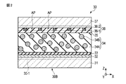
光変調素子30は、透明基板31、下側電極32、配向膜33、光変調層34、配向膜35、上側電極36、および透明基板37を順に備えている。
下側電極32は、例えば、酸化インジウムスズ(ITO;Indium Tin Oxide)や、酸化インジウム亜鉛(IZO;Indium Zinc Oxide)などの透明な導電性材料からなる。透明な導電性材料は、可能な限り可視光の吸収が小さい材料であることが好ましい。反射層36−1は、光反射性を有し、光変調層34側から上側電極36へ入射する光を反射する。反射層36−1は、例えばアルミニウムやチタンなどの金属材料によって構成されている。光吸収層36−2は、可視光を吸収する光吸収性を有し、透明基板37側から上側電極36へ入射する光(外光)を反射する。光吸収層36−2は、例えば黒色樹脂によって構成されている。反射層36−1および光吸収層36−2は、少なくとも一方が導電性を備えている。なお、上側電極36は、光吸収層36−2が導電性を有している場合、反射層36−1を省略することができる。
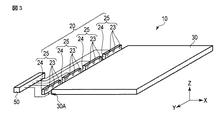
光源20は、例えば、複数の点状光源23を第2方向Yに一列に配置して構成されている。各点状光源23は、光入射面30Aに向かって光を射出するようになっており、例えば、光入射面30Aとの対向面に発光スポットを有する発光素子からなる。そのような発光素子としては、例えば、LED、または、レーザダイオード(LD;Laser Diode)などが挙げられる。
上側電極36は、例えば、複数の帯状の部分電極36Aを互いに並列配置したものである。部分電極36Aは、例えば、第2方向Y、すなわち光入射面30Aと平行な方向に延在し、第1方向X、すなわち光入射面30Aと直交する方向に配列されている。各部分電極36Aは、互いに電気的に分離されており、個別独立に電圧を印加される。なお、複数の部分電極36Aは、互いに電気的に接続されていてもよい。一方、下側電極32は、例えば、光変調層34を介して複数の部分電極36Aと第3方向Zで対向するシート状の電極である。
上側電極36および下側電極32の形状は、特に限定されるものではなく、例えば、下側電極32は、並列配置された複数の部分電極で構成されていてもよい。なお、図示を省略するが、光変調層34に電場を形成する一対の電極は、両方とも光変調層34の同じ側に配置されていてもよい。このような一対の電極は、例えば、第1方向Xまたは第2方向Yに交互に配列され、光変調層34にX−Y平面と平行な横電場を形成する。
部分電極36Aは、複数の開口部APを備えている。開口部APは、図示した例では四角形状となっているが、特に限定されるものではなく、円形状、楕円形状、または多角形状となっていてもよい。開口部APの密度(部分電極36Aのうち単位面積当たりの開口部APの占有率)は、例えば各部分電極36Aにおいて等しいが、各部分電極36Aにおいて異なっていてもよい。開口部APの密度は、開口部APの径および数を変化させることで、制御される。なお、開口部APの密度は、部分電極36Aのパターン密度(部分電極36Aのうち単位面積当たりの開口部AP以外の部分の占有率)より高いことが望ましい。そうすることで、表示装置1は、表示パネルPNLに表示された画像の、光変調素子30における透過率を向上させることができる。
図6は、下側電極32および部分電極36A間に電圧が印加されていない場合の、バルク34Aおよび微粒子34B内の配向状態の一例を模式的に表したものである。
下側電極32および部分電極36A間に電圧が印加されていない時に、光学軸AX2は、光変調素子30の光入射面30Aと平行(またはほぼ平行)となると共に、光照射面30Bと平行(またはほぼ平行)となっている。つまり、下側電極32および上側電極36間に電圧が印加されていない時に、光学軸AX2は、部分電極32Aまたは上側電極36を含む面と平行(またはほぼ平行)となっており、かつ部分電極32Aの延在方向と平行(またはほぼ平行)となっている。
図8は、下側電極32および部分電極36A間に電圧が印加されている時の、バルク34Aおよび微粒子34B内の配向状態の一例を模式的に表したものである。
微粒子34Bは、例えば、下側電極32および部分電極36A間に電圧が印加されている時に、光学軸AX2が光変調素子30の光入射面30Aと平行(もしくはほぼ平行)となると共に光照射面30Bの法線と平行(もしくはほぼ平行)となる構成となっている。つまり、下側電極32および部分電極36A間に電圧が印加されている時に、光学軸AX2は、下側電極32または部分電極36Aを含む面と直交(もしくはほぼ直交)している。
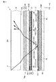
光源20からの光L1(斜め方向からの光)は、光変調素子30内で透明となった透過部分30Tにおいて、界面(透明基板31,37と空気との界面)において全反射され、光変調素子30内を導光される。この結果、透過部分30Tの光照射面30Bの輝度は、光変調素子30が光変調層34を備えていない導光板である場合(図中の一点鎖線)と比べて下がる。
本構成例において、照明装置10は、光源ブロック25および光変調素子30により、光照射面30Bから出射する光の輝度分布を2次元で調整することが可能なローカルディミングを実現することができる。このようなローカルディミングの利用例について説明する。
図示した例においては、高明度部分HBの第1方向Xにおける位置に対応した光源ブロック25が点灯(オン)され、他の光源ブロック25が消灯(オフ)されている。これにより、光変調素子30内の点灯した光源ブロック25に対応する領域には光が導光され、他の領域には光が導光されない。さらに、高明度部分HBの第2方向Yにおける位置に対応したサブエリアSB3,SB4,SB5が図10で上述した散乱部分30Sとなり、他のサブエリアSB1,SB2,SB6が図10で上述した透過部分30Tとなるように、光変調素子30が制御される。すなわち、光変調素子30は、照明領域Aにおいて光が導光されている領域の部分ごとに光の散乱強度を変更する。これにより、照明装置10から出射される光は、高明度部分HBの近辺において輝度が高く、他の部分において輝度が低くなる。
図示した例において、高明度部分HBと重なる面積が最も大きいサブエリアSB4が第1散乱強度I1となり、サブエリアSB4よりも高明度部分HBと重なる面積が小さいサブエリアSB3,SB5が第1散乱強度I1よりも低い第2散乱強度I2(I1>I2)となり、高明度部分HBと重ならないサブエリアSB1,SB2,SB6が第2散乱強度I2よりも低い第3散乱強度I3(I2>I3)となるように光変調素子30が制御されている。図11においては、ハッチングの種類によりこれらの散乱強度を表している。このように、サブエリアSBの散乱強度を多段階で制御することで、より細やかに表示画像のコントラストを調整することができる。
表示パネルPNLは、第1基板SUB1、第2基板SUB2、液晶層LC、および、光学素子ODを備えている。第2基板SUB2は、第1基板SUB1と対向配置されており、第1基板SUB1よりも光変調素子30に近接する側に配置されている。
遮光層BMは、第2絶縁基板200の第1基板SUB1と対向する側に位置している。図示した例では、遮光層BMは、隣り合う画素電極PEの隙間に対向している。カラーフィルタ層CFは、第2絶縁基板200の第1基板SUB1と対向する側に位置し、それらの一部が遮光層BMと重なっている。カラーフィルタ層CFは、詳述しないが、例えば、赤色カラーフィルタ、緑色カラーフィルタ、および、青色カラーフィルタを含んでいる。赤色カラーフィルタは、赤色を表示する画素に配置される。緑色カラーフィルタは、緑色を表示する画素に配置される。青色カラーフィルタは、青色を表示する画素に配置される。なお、カラーフィルタ層CFは、白色などの他の色のカラーフィルタ、あるいは、透明層を含んでいても良い。
光変調素子30内を導光された光L1は、散乱部分30Sで散乱され、光照射面30Bから出射される。偏光板PLの透過軸とバルク34Aの筋状構造の長軸とが互いに平行である場合、光変調層34で散乱された光L1は、偏光板PLの透過軸と平行な方向に偏光している。光照射面30Bから出射された光L1は、偏光板PLを透過する際に偏光度が向上して直線偏光となる。その後、光L1は、位相差板RTを透過する際に円偏光となる。第2基板SUB2を透過する際にカラーフィルタ層CFで着色された光L1は、液晶層LQを透過して画素電極PEで反射され、第2基板SUB2へ向かう。例えば、表示パネルPNLは、オフ状態の時に液晶層LQを透過する光L1の位相を変化させず、オン状態の時に液晶層LQを透過する光L1の位相を変化させる。オフ状態の場合、画素電極PEで反射された光L1は、位相差板RTを透過する際に偏光板PLの透過軸と直交する方向に偏光した直線偏光となり、偏光板PLを透過しない。オン状態の場合、画素電極PEで反射された光L1は、液晶層LQで位相が変化しているため、位相差板RTを透過しても偏光板PLの透過軸と直交する方向に偏光しておらず、偏光板PLを透過する。なお、画素電極PEで反射された光L1は、拡散範囲の拡大、虹色の防止などの目的のために散乱されることが望ましい。例えば、光学素子ODに散乱層が配置され、画素電極PEで反射された光L1は、散乱層によって散乱されてもよい。一方で、図示したように、光L1は、散乱部分30Sで散乱されるため、光学素子ODは、散乱層を備えていなくてもよい。なお、光学素子ODの構成は、図示した例に限らす、他の光学機能層を備えていてもよい。
本変形例は、下側電極32が複数の部分電極32Aを有している点で、図4に図示した構成例と相違している。
本変形例は、部分電極32A,36Aが第2方向Yで不連続に形成されている点で、図13に図示した変形例と相違している。
本変形例は、部分電極32Aの配列方向が図13に図示した変形例と相違している。
本変形例は、開口部APが円形状である点で、図5に図示した構成例と相違している。
本変形例は、開口部APの密度が第1方向Xで異なっている点で、図16に図示した変形例と相違している。
本変形例は、光変調層34が高透過部分34C(第3領域)を備えている点で、図2に図示した構成例と相違している。
30−1…光変調セル 31,37…透明基板 33,35…配向膜
32…下側電極 36…上側電極 36−1…反射層 36−2…光吸収層
34…光変調層 34A…バルク 34B…微粒子
Claims (15)
- 表示面を有し、前記表示面に入射する光を選択的に反射させて画像を表示する表示パネルと、
前記表示パネルの表示面側に配置されその主面内に複数の部分を有する光変調素子と、前記光変調素子の側面に配置された光源と、を備え、前記光源から前記光変調素子に入射した光で前記部分毎に所定輝度で前記表示パネルを照明する照明装置と、
を備えた表示装置。 - 前記光変調素子は、
前記表示パネルに近接する側に配置された第1透明基板と、
前記表示パネルから離れる側に配置された第2透明基板と、
前記第1および第2透明基板の間に位置する光変調層と、
前記光変調層に対して電場を印加するための第1電極および第2電極と、を備え、
前記光変調層は、前記第1および第2電極によって生じる電場の大きさおよび向きに応じて前記光源からの光に対して全体的もしくは部分的に散乱性もしくは透明性を示す、請求項1に記載の表示装置。 - 前記第1および第2電極の少なくとも一方は、前記部分の各々に位置する部分電極を有する、請求項2に記載の表示装置。
- 前記部分電極は、第1方向に並び、
前記光源は、第1方向に交差する第2方向に並んだ複数の点状光源を備えた、請求項3に記載の表示装置。 - 前記表示パネルは、前記照明装置に近接する側に配置された偏光板を備え、
前記光変調層で散乱された光は、前記偏光板の透過軸と平行な方向に偏光している、請求項2に記載の表示装置。 - 表示面を有し、前記表示面に入射する光を選択的に反射させて画像を表示する表示パネルと、
前記表示パネルの表示面側に配置された光変調素子と、前記光変調素子の側面に配置された光源と、を備え、前記光源から前記光変調素子に入射した光で前記表示パネルを照明する照明装置と、を備え、
前記光変調素子は、
前記表示パネルに近接する側に配置された第1透明基板と、
前記表示パネルから離れる側に配置された第2透明基板と、
前記第1および第2透明基板の間に位置する光変調層と、
前記光変調層に対して電場を印加するための第1電極および第2電極と、を備え、
前記光変調層は、前記第1および第2電極によって生じる電場の大きさおよび向きに応じて前記光源からの光に対して全体的もしくは部分的に散乱性もしくは透明性を示す、表示装置。 - 前記第2電極は、前記第2透明基板と前記光変調層との間に位置する反射層と、前記第2透明基板と前記反射層との間に位置し可視光を吸収する光吸収層と、を備えている、請求項2または6に記載の表示装置。
- 前記光変調層は、光学異方性を有すると共に電場に対する応答速度が互いに異なる第1領域および第2領域を有し、
前記第1領域は、液晶材料を主に含んで構成され、
前記第2領域は、高分子材料を主に含んで構成されている、請求項2または6に記載の表示装置。 - 前記表示パネルは、前記照明装置に近接する側に配置された偏光板を備え、
前記第2領域は、前記偏光板の透過軸と平行な方向に長軸を有する筋状構造となっている、請求項8に記載の表示装置。 - 前記第1および第2領域は、前記第1および第2電極に電圧が印加されていない場合に互いに平行となる光学軸を有する、請求項8に記載の表示装置。
- 前記第2領域の前記光学軸は、前記光源から前記光変調素子への光の入射面と平行である、請求項10に記載の表示装置。
- 前記光変調素子は、前記第1および第2電極と前記光変調層との間に水平配向膜を有する、請求項11に記載の表示装置。
- 前記光変調層は、前記光変調層の主面に垂直な厚さ方向の散乱が前記光変調層の主面と平行な方向の散乱よりも大きい異方性散乱特性を有する、請求項12に記載の表示装置。
- 前記第1および第2領域の常光屈折率が互いに等しく、かつ前記第1および第2領域の異常光屈折率が互いに等しい、請求項8に記載の表示装置。
- 前記光変調層は、さらに、前記第1および第2領域よりも光透過率が高い樹脂材料によって形成された第3領域を有する、請求項8に記載の表示装置。
Priority Applications (7)
| Application Number | Priority Date | Filing Date | Title |
|---|---|---|---|
| JP2015238496A JP6671940B2 (ja) | 2015-12-07 | 2015-12-07 | 表示装置 |
| CN201611110743.XA CN107037632B (zh) | 2015-12-07 | 2016-12-06 | 显示装置 |
| CN202010897438.XA CN111965879B (zh) | 2015-12-07 | 2016-12-06 | 光调制元件 |
| US15/371,569 US9983437B2 (en) | 2015-12-07 | 2016-12-07 | Display device including an optical modulator |
| US15/958,799 US10303000B2 (en) | 2015-12-07 | 2018-04-20 | Display device including an optical modulator |
| US16/385,310 US10503013B2 (en) | 2015-12-07 | 2019-04-16 | Display device including an optical modulator |
| JP2020036816A JP6938699B2 (ja) | 2015-12-07 | 2020-03-04 | 電子機器 |
Applications Claiming Priority (1)
| Application Number | Priority Date | Filing Date | Title |
|---|---|---|---|
| JP2015238496A JP6671940B2 (ja) | 2015-12-07 | 2015-12-07 | 表示装置 |
Related Child Applications (1)
| Application Number | Title | Priority Date | Filing Date |
|---|---|---|---|
| JP2020036816A Division JP6938699B2 (ja) | 2015-12-07 | 2020-03-04 | 電子機器 |
Publications (2)
| Publication Number | Publication Date |
|---|---|
| JP2017106962A true JP2017106962A (ja) | 2017-06-15 |
| JP6671940B2 JP6671940B2 (ja) | 2020-03-25 |
Family
ID=58798241
Family Applications (1)
| Application Number | Title | Priority Date | Filing Date |
|---|---|---|---|
| JP2015238496A Active JP6671940B2 (ja) | 2015-12-07 | 2015-12-07 | 表示装置 |
Country Status (3)
| Country | Link |
|---|---|
| US (3) | US9983437B2 (ja) |
| JP (1) | JP6671940B2 (ja) |
| CN (2) | CN107037632B (ja) |
Families Citing this family (18)
| Publication number | Priority date | Publication date | Assignee | Title |
|---|---|---|---|---|
| US10466538B2 (en) | 2016-03-15 | 2019-11-05 | Japan Display Inc. | Display device |
| JP6716323B2 (ja) | 2016-04-01 | 2020-07-01 | 株式会社ジャパンディスプレイ | 表示装置 |
| JP6720008B2 (ja) * | 2016-07-22 | 2020-07-08 | 株式会社ジャパンディスプレイ | 表示装置および表示装置の駆動方法 |
| JP6800641B2 (ja) * | 2016-07-22 | 2020-12-16 | 株式会社ジャパンディスプレイ | 表示装置 |
| JP6877910B2 (ja) | 2016-08-01 | 2021-05-26 | 株式会社ジャパンディスプレイ | 表示装置 |
| CN106990871A (zh) * | 2017-04-13 | 2017-07-28 | 京东方科技集团股份有限公司 | 一种触控面板及其制备方法、显示面板和显示装置 |
| JP7005243B2 (ja) | 2017-09-14 | 2022-01-21 | 株式会社ジャパンディスプレイ | 表示装置 |
| KR101977233B1 (ko) * | 2017-09-29 | 2019-08-28 | 엘지디스플레이 주식회사 | 반사 전극, 그 제조 방법 및 반사 전극을 포함하는 유기발광 다이오드 표시장치 |
| JP7083675B2 (ja) | 2018-03-23 | 2022-06-13 | 株式会社ジャパンディスプレイ | 表示装置 |
| JP7109956B2 (ja) | 2018-03-27 | 2022-08-01 | 株式会社ジャパンディスプレイ | 表示装置 |
| JP7109955B2 (ja) | 2018-03-27 | 2022-08-01 | 株式会社ジャパンディスプレイ | 表示装置 |
| JP7109957B2 (ja) * | 2018-03-27 | 2022-08-01 | 株式会社ジャパンディスプレイ | 表示装置 |
| JP7118790B2 (ja) * | 2018-07-24 | 2022-08-16 | 株式会社ジャパンディスプレイ | 表示装置 |
| CN109739040B (zh) * | 2019-02-25 | 2021-08-27 | 京东方科技集团股份有限公司 | 一种调光片、背光模组、显示装置及其驱动方法 |
| JP7222835B2 (ja) * | 2019-07-10 | 2023-02-15 | 株式会社ジャパンディスプレイ | 表示装置 |
| JP2021033017A (ja) * | 2019-08-22 | 2021-03-01 | 株式会社ジャパンディスプレイ | 表示装置 |
| US11733598B2 (en) * | 2019-12-04 | 2023-08-22 | Liqxtal Technology Inc. | Tunable light projector |
| JP2024073087A (ja) * | 2022-11-17 | 2024-05-29 | 株式会社ジャパンディスプレイ | 表示装置 |
Citations (5)
| Publication number | Priority date | Publication date | Assignee | Title |
|---|---|---|---|---|
| JPH07199184A (ja) * | 1993-12-28 | 1995-08-04 | Nec Corp | 表示装置 |
| JP2005265920A (ja) * | 2004-03-16 | 2005-09-29 | Seiko Epson Corp | 電気光学装置、電子機器 |
| KR20080006690A (ko) * | 2006-07-13 | 2008-01-17 | 삼성전자주식회사 | 액정 표시 장치 |
| US20110149201A1 (en) * | 2009-10-16 | 2011-06-23 | Karlton David Powell | Lightguide illuminator embedded display |
| JP2012252993A (ja) * | 2011-05-10 | 2012-12-20 | Sony Corp | 照明装置および表示装置 |
Family Cites Families (38)
| Publication number | Priority date | Publication date | Assignee | Title |
|---|---|---|---|---|
| JPH08304788A (ja) * | 1995-05-02 | 1996-11-22 | Minolta Co Ltd | 高分子分散型液晶素子 |
| JP3172510B2 (ja) * | 1998-07-28 | 2001-06-04 | 日本電信電話株式会社 | 光学素子および該光学素子を用いた表示装置 |
| JP3410977B2 (ja) | 1998-09-14 | 2003-05-26 | シャープ株式会社 | フロントライト及び反射型液晶表示装置 |
| JP4476505B2 (ja) * | 2001-02-09 | 2010-06-09 | シャープ株式会社 | 液晶表示装置 |
| JP2003043482A (ja) | 2001-08-01 | 2003-02-13 | Fuji Photo Film Co Ltd | 反射型液晶表示装置 |
| JP4437920B2 (ja) | 2001-09-26 | 2010-03-24 | コーニンクレッカ フィリップス エレクトロニクス エヌ ヴィ | 偏光を供給するための微細構造化された照明システム |
| JP2006201280A (ja) | 2005-01-18 | 2006-08-03 | Seiko Instruments Inc | 液晶表示装置 |
| WO2007040028A1 (ja) * | 2005-10-04 | 2007-04-12 | Sharp Kabushiki Kaisha | 液晶表示装置およびそれを備えた携帯型電子機器 |
| CN102150076A (zh) * | 2008-09-25 | 2011-08-10 | 夏普株式会社 | 光量调整装置、背光源单元、液晶显示面板和液晶显示装置 |
| JP5263593B2 (ja) | 2008-10-07 | 2013-08-14 | ソニー株式会社 | 照明装置および表示装置 |
| KR101536221B1 (ko) * | 2008-11-20 | 2015-07-14 | 삼성디스플레이 주식회사 | 픽셀 데이터 보상 방법, 이를 수행하기 위한 콘트롤러 유닛및 이를 갖는 표시 장치 |
| JP4752911B2 (ja) | 2008-12-26 | 2011-08-17 | ソニー株式会社 | 照明装置、表示装置、およびエッジライト方式のバックライトに用いる光変調素子の製造方法 |
| JP2010157475A (ja) * | 2009-01-05 | 2010-07-15 | Sony Corp | 照明装置および表示装置 |
| US9035975B2 (en) * | 2009-10-14 | 2015-05-19 | Dolby Laboratories Licensing Corporation | Variable flower display backlight system |
| JP5467389B2 (ja) | 2009-11-06 | 2014-04-09 | ソニー株式会社 | 照明装置および表示装置 |
| JP5756931B2 (ja) | 2009-12-11 | 2015-07-29 | ソニー株式会社 | 照明装置および表示装置 |
| JP5467388B2 (ja) * | 2010-04-06 | 2014-04-09 | ソニー株式会社 | 照明装置および表示装置 |
| US9720345B2 (en) | 2010-06-02 | 2017-08-01 | Canon Kabushiki Kaisha | Image forming apparatus |
| US8768202B2 (en) | 2010-06-02 | 2014-07-01 | Canon Kabushiki Kaisha | Image forming apparatus |
| JP5825847B2 (ja) | 2010-06-02 | 2015-12-02 | キヤノン株式会社 | 画像形成装置 |
| JP2012088486A (ja) | 2010-10-19 | 2012-05-10 | Sony Corp | 表示パネルおよび表示装置 |
| JP5516319B2 (ja) | 2010-10-20 | 2014-06-11 | ソニー株式会社 | 照明装置および表示装置 |
| JP5699786B2 (ja) | 2011-04-28 | 2015-04-15 | ソニー株式会社 | 表示装置および照明装置 |
| JP2014517931A (ja) * | 2011-04-28 | 2014-07-24 | ドルビー ラボラトリーズ ライセンシング コーポレイション | クロスbefコリメータおよび偏光保存拡散器を備えるデュアルパネルディスプレイ |
| JP2012234725A (ja) * | 2011-05-02 | 2012-11-29 | Sony Corp | 表示装置および照明装置 |
| JP5948813B2 (ja) | 2011-05-09 | 2016-07-06 | ソニー株式会社 | 照明装置および表示装置 |
| JP6267118B2 (ja) * | 2011-08-24 | 2018-01-24 | ドルビー ラボラトリーズ ライセンシング コーポレイション | 広色域及びエネルギー効率を有する高ダイナミックレンジディスプレイ |
| JP5817989B2 (ja) | 2011-10-05 | 2015-11-18 | ソニー株式会社 | 照明装置、表示装置および電子機器 |
| EP2766894A1 (en) * | 2011-10-13 | 2014-08-20 | Dolby Laboratories Licensing Corporation | Methods and apparatus for backlighting dual modulation display devices |
| TW201400946A (zh) | 2012-05-09 | 2014-01-01 | Sony Corp | 照明裝置及顯示裝置 |
| TWI545377B (zh) * | 2012-05-11 | 2016-08-11 | Sony Corp | Lighting device and display device |
| JP6098064B2 (ja) | 2012-08-08 | 2017-03-22 | ソニー株式会社 | 表示装置および照明装置 |
| JP5954097B2 (ja) * | 2012-10-11 | 2016-07-20 | ソニー株式会社 | 表示装置 |
| JP5963884B2 (ja) * | 2012-12-20 | 2016-08-03 | 三菱電機株式会社 | 液晶表示装置 |
| US9224323B2 (en) * | 2013-05-06 | 2015-12-29 | Dolby Laboratories Licensing Corporation | Systems and methods for increasing spatial or temporal resolution for dual modulated display systems |
| JP6118212B2 (ja) * | 2013-08-12 | 2017-04-19 | 富士フイルム株式会社 | 液晶表示装置 |
| WO2015088900A1 (en) * | 2013-12-10 | 2015-06-18 | Dolby Laboratories Licensing Corporation | Laser diode driven lcd quantum dot hybrid displays |
| US10216034B2 (en) * | 2014-06-13 | 2019-02-26 | Sharp Kabushiki Kaisha | Liquid crystal display device |
-
2015
- 2015-12-07 JP JP2015238496A patent/JP6671940B2/ja active Active
-
2016
- 2016-12-06 CN CN201611110743.XA patent/CN107037632B/zh active Active
- 2016-12-06 CN CN202010897438.XA patent/CN111965879B/zh active Active
- 2016-12-07 US US15/371,569 patent/US9983437B2/en active Active
-
2018
- 2018-04-20 US US15/958,799 patent/US10303000B2/en active Active
-
2019
- 2019-04-16 US US16/385,310 patent/US10503013B2/en active Active
Patent Citations (5)
| Publication number | Priority date | Publication date | Assignee | Title |
|---|---|---|---|---|
| JPH07199184A (ja) * | 1993-12-28 | 1995-08-04 | Nec Corp | 表示装置 |
| JP2005265920A (ja) * | 2004-03-16 | 2005-09-29 | Seiko Epson Corp | 電気光学装置、電子機器 |
| KR20080006690A (ko) * | 2006-07-13 | 2008-01-17 | 삼성전자주식회사 | 액정 표시 장치 |
| US20110149201A1 (en) * | 2009-10-16 | 2011-06-23 | Karlton David Powell | Lightguide illuminator embedded display |
| JP2012252993A (ja) * | 2011-05-10 | 2012-12-20 | Sony Corp | 照明装置および表示装置 |
Also Published As
| Publication number | Publication date |
|---|---|
| CN107037632B (zh) | 2020-09-22 |
| CN107037632A (zh) | 2017-08-11 |
| US10503013B2 (en) | 2019-12-10 |
| CN111965879A (zh) | 2020-11-20 |
| US20190243189A1 (en) | 2019-08-08 |
| CN111965879B (zh) | 2023-09-29 |
| JP6671940B2 (ja) | 2020-03-25 |
| US10303000B2 (en) | 2019-05-28 |
| US20170160592A1 (en) | 2017-06-08 |
| US20180239198A1 (en) | 2018-08-23 |
| US9983437B2 (en) | 2018-05-29 |
Similar Documents
| Publication | Publication Date | Title |
|---|---|---|
| JP6671940B2 (ja) | 表示装置 | |
| JP6112108B2 (ja) | 照明装置および表示装置 | |
| JP5263593B2 (ja) | 照明装置および表示装置 | |
| KR101712677B1 (ko) | 조명 장치 및 디스플레이 장치 | |
| JP3900805B2 (ja) | 照明装置及びそれを用いた液晶表示装置 | |
| US9581749B2 (en) | Lighting unit, display, and three-dimensional display | |
| JP5954097B2 (ja) | 表示装置 | |
| CN102686932B (zh) | 照明单元和显示器 | |
| JP2010157475A (ja) | 照明装置および表示装置 | |
| JP5910042B2 (ja) | 照明装置および表示装置 | |
| JP6035866B2 (ja) | 照明装置および表示装置 | |
| CN110646982A (zh) | 液晶显示面板及其驱动方法、显示装置 | |
| JP6938699B2 (ja) | 電子機器 | |
| JP2021096996A (ja) | 車両用灯具システム |
Legal Events
| Date | Code | Title | Description |
|---|---|---|---|
| A621 | Written request for application examination |
Free format text: JAPANESE INTERMEDIATE CODE: A621 Effective date: 20181009 |
|
| A977 | Report on retrieval |
Free format text: JAPANESE INTERMEDIATE CODE: A971007 Effective date: 20190808 |
|
| A131 | Notification of reasons for refusal |
Free format text: JAPANESE INTERMEDIATE CODE: A131 Effective date: 20190820 |
|
| A521 | Request for written amendment filed |
Free format text: JAPANESE INTERMEDIATE CODE: A523 Effective date: 20191009 |
|
| TRDD | Decision of grant or rejection written | ||
| A01 | Written decision to grant a patent or to grant a registration (utility model) |
Free format text: JAPANESE INTERMEDIATE CODE: A01 Effective date: 20200204 |
|
| A61 | First payment of annual fees (during grant procedure) |
Free format text: JAPANESE INTERMEDIATE CODE: A61 Effective date: 20200304 |
|
| R150 | Certificate of patent or registration of utility model |
Ref document number: 6671940 Country of ref document: JP Free format text: JAPANESE INTERMEDIATE CODE: R150 |
|
| R250 | Receipt of annual fees |
Free format text: JAPANESE INTERMEDIATE CODE: R250 |
|
| R250 | Receipt of annual fees |
Free format text: JAPANESE INTERMEDIATE CODE: R250 |
|
| R250 | Receipt of annual fees |
Free format text: JAPANESE INTERMEDIATE CODE: R250 |
|
| R250 | Receipt of annual fees |
Free format text: JAPANESE INTERMEDIATE CODE: R250 |