JP5516319B2 - 照明装置および表示装置 - Google Patents
照明装置および表示装置 Download PDFInfo
- Publication number
- JP5516319B2 JP5516319B2 JP2010235925A JP2010235925A JP5516319B2 JP 5516319 B2 JP5516319 B2 JP 5516319B2 JP 2010235925 A JP2010235925 A JP 2010235925A JP 2010235925 A JP2010235925 A JP 2010235925A JP 5516319 B2 JP5516319 B2 JP 5516319B2
- Authority
- JP
- Japan
- Prior art keywords
- electrode
- light
- light source
- guide plate
- light guide
- Prior art date
- Legal status (The legal status is an assumption and is not a legal conclusion. Google has not performed a legal analysis and makes no representation as to the accuracy of the status listed.)
- Expired - Fee Related
Links
Images


Classifications
-
- G—PHYSICS
- G02—OPTICS
- G02F—OPTICAL DEVICES OR ARRANGEMENTS FOR THE CONTROL OF LIGHT BY MODIFICATION OF THE OPTICAL PROPERTIES OF THE MEDIA OF THE ELEMENTS INVOLVED THEREIN; NON-LINEAR OPTICS; FREQUENCY-CHANGING OF LIGHT; OPTICAL LOGIC ELEMENTS; OPTICAL ANALOGUE/DIGITAL CONVERTERS
- G02F1/00—Devices or arrangements for the control of the intensity, colour, phase, polarisation or direction of light arriving from an independent light source, e.g. switching, gating or modulating; Non-linear optics
- G02F1/01—Devices or arrangements for the control of the intensity, colour, phase, polarisation or direction of light arriving from an independent light source, e.g. switching, gating or modulating; Non-linear optics for the control of the intensity, phase, polarisation or colour
- G02F1/13—Devices or arrangements for the control of the intensity, colour, phase, polarisation or direction of light arriving from an independent light source, e.g. switching, gating or modulating; Non-linear optics for the control of the intensity, phase, polarisation or colour based on liquid crystals, e.g. single liquid crystal display cells
- G02F1/133—Constructional arrangements; Operation of liquid crystal cells; Circuit arrangements
- G02F1/1333—Constructional arrangements; Manufacturing methods
- G02F1/1335—Structural association of cells with optical devices, e.g. polarisers or reflectors
- G02F1/1336—Illuminating devices
- G02F1/133615—Edge-illuminating devices, i.e. illuminating from the side
-
- G—PHYSICS
- G02—OPTICS
- G02B—OPTICAL ELEMENTS, SYSTEMS OR APPARATUS
- G02B6/00—Light guides; Structural details of arrangements comprising light guides and other optical elements, e.g. couplings
- G02B6/0001—Light guides; Structural details of arrangements comprising light guides and other optical elements, e.g. couplings specially adapted for lighting devices or systems
- G02B6/0011—Light guides; Structural details of arrangements comprising light guides and other optical elements, e.g. couplings specially adapted for lighting devices or systems the light guides being planar or of plate-like form
- G02B6/0013—Means for improving the coupling-in of light from the light source into the light guide
-
- G—PHYSICS
- G02—OPTICS
- G02B—OPTICAL ELEMENTS, SYSTEMS OR APPARATUS
- G02B6/00—Light guides; Structural details of arrangements comprising light guides and other optical elements, e.g. couplings
- G02B6/0001—Light guides; Structural details of arrangements comprising light guides and other optical elements, e.g. couplings specially adapted for lighting devices or systems
- G02B6/0011—Light guides; Structural details of arrangements comprising light guides and other optical elements, e.g. couplings specially adapted for lighting devices or systems the light guides being planar or of plate-like form
- G02B6/0033—Means for improving the coupling-out of light from the light guide
- G02B6/0035—Means for improving the coupling-out of light from the light guide provided on the surface of the light guide or in the bulk of it
- G02B6/0036—2-D arrangement of prisms, protrusions, indentations or roughened surfaces
-
- G—PHYSICS
- G02—OPTICS
- G02F—OPTICAL DEVICES OR ARRANGEMENTS FOR THE CONTROL OF LIGHT BY MODIFICATION OF THE OPTICAL PROPERTIES OF THE MEDIA OF THE ELEMENTS INVOLVED THEREIN; NON-LINEAR OPTICS; FREQUENCY-CHANGING OF LIGHT; OPTICAL LOGIC ELEMENTS; OPTICAL ANALOGUE/DIGITAL CONVERTERS
- G02F1/00—Devices or arrangements for the control of the intensity, colour, phase, polarisation or direction of light arriving from an independent light source, e.g. switching, gating or modulating; Non-linear optics
- G02F1/01—Devices or arrangements for the control of the intensity, colour, phase, polarisation or direction of light arriving from an independent light source, e.g. switching, gating or modulating; Non-linear optics for the control of the intensity, phase, polarisation or colour
- G02F1/13—Devices or arrangements for the control of the intensity, colour, phase, polarisation or direction of light arriving from an independent light source, e.g. switching, gating or modulating; Non-linear optics for the control of the intensity, phase, polarisation or colour based on liquid crystals, e.g. single liquid crystal display cells
- G02F1/133—Constructional arrangements; Operation of liquid crystal cells; Circuit arrangements
- G02F1/1333—Constructional arrangements; Manufacturing methods
- G02F1/1343—Electrodes
- G02F1/134309—Electrodes characterised by their geometrical arrangement
-
- G—PHYSICS
- G09—EDUCATION; CRYPTOGRAPHY; DISPLAY; ADVERTISING; SEALS
- G09G—ARRANGEMENTS OR CIRCUITS FOR CONTROL OF INDICATING DEVICES USING STATIC MEANS TO PRESENT VARIABLE INFORMATION
- G09G3/00—Control arrangements or circuits, of interest only in connection with visual indicators other than cathode-ray tubes
- G09G3/20—Control arrangements or circuits, of interest only in connection with visual indicators other than cathode-ray tubes for presentation of an assembly of a number of characters, e.g. a page, by composing the assembly by combination of individual elements arranged in a matrix no fixed position being assigned to or needed to be assigned to the individual characters or partial characters
- G09G3/34—Control arrangements or circuits, of interest only in connection with visual indicators other than cathode-ray tubes for presentation of an assembly of a number of characters, e.g. a page, by composing the assembly by combination of individual elements arranged in a matrix no fixed position being assigned to or needed to be assigned to the individual characters or partial characters by control of light from an independent source
- G09G3/3406—Control of illumination source
- G09G3/342—Control of illumination source using several illumination sources separately controlled corresponding to different display panel areas, e.g. along one dimension such as lines
-
- G—PHYSICS
- G02—OPTICS
- G02B—OPTICAL ELEMENTS, SYSTEMS OR APPARATUS
- G02B6/00—Light guides; Structural details of arrangements comprising light guides and other optical elements, e.g. couplings
- G02B6/0001—Light guides; Structural details of arrangements comprising light guides and other optical elements, e.g. couplings specially adapted for lighting devices or systems
- G02B6/0011—Light guides; Structural details of arrangements comprising light guides and other optical elements, e.g. couplings specially adapted for lighting devices or systems the light guides being planar or of plate-like form
- G02B6/0013—Means for improving the coupling-in of light from the light source into the light guide
- G02B6/0023—Means for improving the coupling-in of light from the light source into the light guide provided by one optical element, or plurality thereof, placed between the light guide and the light source, or around the light source
- G02B6/0028—Light guide, e.g. taper
-
- G—PHYSICS
- G02—OPTICS
- G02B—OPTICAL ELEMENTS, SYSTEMS OR APPARATUS
- G02B6/00—Light guides; Structural details of arrangements comprising light guides and other optical elements, e.g. couplings
- G02B6/0001—Light guides; Structural details of arrangements comprising light guides and other optical elements, e.g. couplings specially adapted for lighting devices or systems
- G02B6/0011—Light guides; Structural details of arrangements comprising light guides and other optical elements, e.g. couplings specially adapted for lighting devices or systems the light guides being planar or of plate-like form
- G02B6/0033—Means for improving the coupling-out of light from the light guide
- G02B6/0035—Means for improving the coupling-out of light from the light guide provided on the surface of the light guide or in the bulk of it
- G02B6/0038—Linear indentations or grooves, e.g. arc-shaped grooves or meandering grooves, extending over the full length or width of the light guide
-
- G—PHYSICS
- G02—OPTICS
- G02B—OPTICAL ELEMENTS, SYSTEMS OR APPARATUS
- G02B6/00—Light guides; Structural details of arrangements comprising light guides and other optical elements, e.g. couplings
- G02B6/0001—Light guides; Structural details of arrangements comprising light guides and other optical elements, e.g. couplings specially adapted for lighting devices or systems
- G02B6/0011—Light guides; Structural details of arrangements comprising light guides and other optical elements, e.g. couplings specially adapted for lighting devices or systems the light guides being planar or of plate-like form
- G02B6/0033—Means for improving the coupling-out of light from the light guide
- G02B6/0035—Means for improving the coupling-out of light from the light guide provided on the surface of the light guide or in the bulk of it
- G02B6/004—Scattering dots or dot-like elements, e.g. microbeads, scattering particles, nanoparticles
- G02B6/0041—Scattering dots or dot-like elements, e.g. microbeads, scattering particles, nanoparticles provided in the bulk of the light guide
-
- G—PHYSICS
- G02—OPTICS
- G02B—OPTICAL ELEMENTS, SYSTEMS OR APPARATUS
- G02B6/00—Light guides; Structural details of arrangements comprising light guides and other optical elements, e.g. couplings
- G02B6/0001—Light guides; Structural details of arrangements comprising light guides and other optical elements, e.g. couplings specially adapted for lighting devices or systems
- G02B6/0011—Light guides; Structural details of arrangements comprising light guides and other optical elements, e.g. couplings specially adapted for lighting devices or systems the light guides being planar or of plate-like form
- G02B6/0033—Means for improving the coupling-out of light from the light guide
- G02B6/0035—Means for improving the coupling-out of light from the light guide provided on the surface of the light guide or in the bulk of it
- G02B6/004—Scattering dots or dot-like elements, e.g. microbeads, scattering particles, nanoparticles
- G02B6/0043—Scattering dots or dot-like elements, e.g. microbeads, scattering particles, nanoparticles provided on the surface of the light guide
-
- G—PHYSICS
- G02—OPTICS
- G02B—OPTICAL ELEMENTS, SYSTEMS OR APPARATUS
- G02B6/00—Light guides; Structural details of arrangements comprising light guides and other optical elements, e.g. couplings
- G02B6/0001—Light guides; Structural details of arrangements comprising light guides and other optical elements, e.g. couplings specially adapted for lighting devices or systems
- G02B6/0011—Light guides; Structural details of arrangements comprising light guides and other optical elements, e.g. couplings specially adapted for lighting devices or systems the light guides being planar or of plate-like form
- G02B6/0033—Means for improving the coupling-out of light from the light guide
- G02B6/0058—Means for improving the coupling-out of light from the light guide varying in density, size, shape or depth along the light guide
-
- G—PHYSICS
- G02—OPTICS
- G02F—OPTICAL DEVICES OR ARRANGEMENTS FOR THE CONTROL OF LIGHT BY MODIFICATION OF THE OPTICAL PROPERTIES OF THE MEDIA OF THE ELEMENTS INVOLVED THEREIN; NON-LINEAR OPTICS; FREQUENCY-CHANGING OF LIGHT; OPTICAL LOGIC ELEMENTS; OPTICAL ANALOGUE/DIGITAL CONVERTERS
- G02F1/00—Devices or arrangements for the control of the intensity, colour, phase, polarisation or direction of light arriving from an independent light source, e.g. switching, gating or modulating; Non-linear optics
- G02F1/01—Devices or arrangements for the control of the intensity, colour, phase, polarisation or direction of light arriving from an independent light source, e.g. switching, gating or modulating; Non-linear optics for the control of the intensity, phase, polarisation or colour
- G02F1/13—Devices or arrangements for the control of the intensity, colour, phase, polarisation or direction of light arriving from an independent light source, e.g. switching, gating or modulating; Non-linear optics for the control of the intensity, phase, polarisation or colour based on liquid crystals, e.g. single liquid crystal display cells
- G02F1/133—Constructional arrangements; Operation of liquid crystal cells; Circuit arrangements
- G02F1/1333—Constructional arrangements; Manufacturing methods
- G02F1/1334—Constructional arrangements; Manufacturing methods based on polymer dispersed liquid crystals, e.g. microencapsulated liquid crystals
-
- G—PHYSICS
- G02—OPTICS
- G02F—OPTICAL DEVICES OR ARRANGEMENTS FOR THE CONTROL OF LIGHT BY MODIFICATION OF THE OPTICAL PROPERTIES OF THE MEDIA OF THE ELEMENTS INVOLVED THEREIN; NON-LINEAR OPTICS; FREQUENCY-CHANGING OF LIGHT; OPTICAL LOGIC ELEMENTS; OPTICAL ANALOGUE/DIGITAL CONVERTERS
- G02F1/00—Devices or arrangements for the control of the intensity, colour, phase, polarisation or direction of light arriving from an independent light source, e.g. switching, gating or modulating; Non-linear optics
- G02F1/01—Devices or arrangements for the control of the intensity, colour, phase, polarisation or direction of light arriving from an independent light source, e.g. switching, gating or modulating; Non-linear optics for the control of the intensity, phase, polarisation or colour
- G02F1/13—Devices or arrangements for the control of the intensity, colour, phase, polarisation or direction of light arriving from an independent light source, e.g. switching, gating or modulating; Non-linear optics for the control of the intensity, phase, polarisation or colour based on liquid crystals, e.g. single liquid crystal display cells
- G02F1/133—Constructional arrangements; Operation of liquid crystal cells; Circuit arrangements
- G02F1/1333—Constructional arrangements; Manufacturing methods
- G02F1/1335—Structural association of cells with optical devices, e.g. polarisers or reflectors
- G02F1/1336—Illuminating devices
- G02F1/133601—Illuminating devices for spatial active dimming
-
- G—PHYSICS
- G02—OPTICS
- G02F—OPTICAL DEVICES OR ARRANGEMENTS FOR THE CONTROL OF LIGHT BY MODIFICATION OF THE OPTICAL PROPERTIES OF THE MEDIA OF THE ELEMENTS INVOLVED THEREIN; NON-LINEAR OPTICS; FREQUENCY-CHANGING OF LIGHT; OPTICAL LOGIC ELEMENTS; OPTICAL ANALOGUE/DIGITAL CONVERTERS
- G02F1/00—Devices or arrangements for the control of the intensity, colour, phase, polarisation or direction of light arriving from an independent light source, e.g. switching, gating or modulating; Non-linear optics
- G02F1/01—Devices or arrangements for the control of the intensity, colour, phase, polarisation or direction of light arriving from an independent light source, e.g. switching, gating or modulating; Non-linear optics for the control of the intensity, phase, polarisation or colour
- G02F1/13—Devices or arrangements for the control of the intensity, colour, phase, polarisation or direction of light arriving from an independent light source, e.g. switching, gating or modulating; Non-linear optics for the control of the intensity, phase, polarisation or colour based on liquid crystals, e.g. single liquid crystal display cells
- G02F1/133—Constructional arrangements; Operation of liquid crystal cells; Circuit arrangements
- G02F1/1333—Constructional arrangements; Manufacturing methods
- G02F1/1343—Electrodes
- G02F1/134309—Electrodes characterised by their geometrical arrangement
- G02F1/134318—Electrodes characterised by their geometrical arrangement having a patterned common electrode
Landscapes
- Physics & Mathematics (AREA)
- General Physics & Mathematics (AREA)
- Optics & Photonics (AREA)
- Nonlinear Science (AREA)
- Engineering & Computer Science (AREA)
- Mathematical Physics (AREA)
- Chemical & Material Sciences (AREA)
- Crystallography & Structural Chemistry (AREA)
- Theoretical Computer Science (AREA)
- Computer Hardware Design (AREA)
- Geometry (AREA)
- Planar Illumination Modules (AREA)
- Liquid Crystal (AREA)
Description
1.第1の実施の形態(図1〜図15)
バックライト内に、水平配向膜を含む光変調素子が設けられている例
2.第2の実施の形態(図16〜図18)
バックライト内に、垂直配向膜を含む光変調素子が設けられている例
3.変形例
下側電極の辺部に凹凸が形成されている例(図19〜図21)
上側電極に開口が形成されている例(図22〜図26)
下側電極の辺部に凹凸が形成され、かつ上側電極に開口が形成されている例
(図27〜図32)
下側電極の辺部に凹凸が形成され、かつ下側電極に開口が形成されている例
(図33,図34)
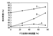
ITO面積および散乱強度が変更されている例(図35)
下側電極の辺部に凹凸が形成され、かつ下側電極に開口と金属線が
形成されている例(図36)
下側電極と上側電極に開口が形成されている例(図37)
光変調素子の位置が異なる例(図38〜図40)
4.実施例・比較例(図41〜図75)
5.適用例(図76)
上記実施の形態等のバックライトが表示装置の光源として適用されている例
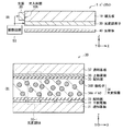
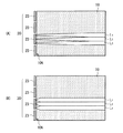
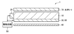
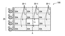
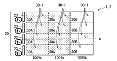
図1(A)は、本発明の第1の実施の形態に係るバックライト1(照明装置)の概略構成の一例を表す断面図である。図1(B)は、図1(A)のバックライト1に搭載された光変調素子30(後述)の構成の一例を表す断面図である。なお、図1(A),(B)は、模式的に表したものであり、実際の寸法や形状と同一であるとは限らない。バックライト1は、例えば、液晶表示パネルなどを背後から照明するものであり、導光板10と、導光板10の側面に配置した光源20と、導光板10の背後に配置した光変調素子30および反射板40と、光源20および光変調素子30を駆動する駆動回路50とを備えている。
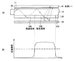
図16(A)は、本発明の第2の実施の形態に係るバックライト2(照明装置)の概略構成の一例を表す断面図である。図16(B)は、図16(A)のバックライト2の詳細な構成の一例を表す断面図である。なお、図16(A),(B)は、模式的に表したものであり、実際の寸法や形状と同一であるとは限らない。
[第1変形例]
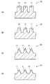
上記各実施の形態では、各部分電極32Aが矩形状となっていたが、各部分電極32Aの辺部(エッジ)の形状が非直線状となっていてもよい。例えば、各部分電極32Aは、他の部分電極32Aに隣接する辺部に、凹凸形状(凹凸部32B)を有していてもよい。凹凸部32Bは、例えば、図19に示したように、ジグザグ形状となっていてもよいし、例えば、図20(A)〜(D)に示したように、曲線形状、ランプ形状、台形状またはランダム形状となっていてもよい。
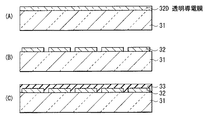
上記各実施の形態において、上側電極36または部分電極36Aがパターニングされていてもよい。これにより、照明光の面内輝度の均一化を行うことが出来る。さらに、電極の面積が減ることにより、上側電極36または部分電極36AがITOなどからなる場合に、電極による可視光の吸収を低減することが可能となる。
1<(D1/D2)<(β側の部分電極32Aに掛かる電圧のデューティ比(例えば図中の50%))/(α側の部分電極32Aに掛かる電圧のデューティ比(例えば図中の25%))
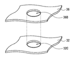
上記各実施の形態において、各部分電極32Aが、他の部分電極32Aに隣接する辺部に、凹凸形状(凹凸部32B)を有し、さらに、パターニングされていてもよい。各部分電極32Aに対して、例えば、図33(A),(B)に示したように、複数の開口32Cが設けられていてもよい。このとき、開口32Cが、例えば、図33(A)に示したように、部分電極32Aのうち凹凸部32B以外の部分にだけ形成されていてもよいし、例えば、図33(B)に示したように、凹凸部32Bを含む部分電極32A全体に形成されていてもよい。いずれの場合においても、下側電極32のうち凹凸部32Bを含む部分における開口32Cおよびスリット部の密度と、部分電極32Aのうち凹凸部32B以外の部分における開口32Cの密度とが互いに等しくなっていることが好ましい。
導光板:n=1.49,厚み5mm
透明基板:n=1.53,厚み0.1mm
電極(ITO):n=2.0
光変調層:面に垂直に入射する光に対してヘイズ33%(実測値)の散乱
構成:導光板の裏面に光変調素子、反射シートあり、
導光板の上面に拡散シート、プリズムシートあり
バックライトのサイズ:40インチ
上記各実施の形態において、各部分電極32Aおよび上側電極36または部分電極36Aに対して、開口32C,36Bが形成されていてもよい。これにより、各部分電極32Aおよび上側電極36または部分電極36AがITOなどからなる場合に、電極による可視光の吸収を低減することが可能となる。
上記実施の形態等では、光変調素子30,60は、導光板10の背後(下面)に空気層を介さずに密着して接合されていたが、例えば、図38に示したように、導光板10の上面に空気層を介さずに密着して接合されていてもよい。また、光変調素子30,60は、例えば、図39に示したように、導光板10の内部に設けられていてもよい。ただし、この場合でも、光変調素子30,60は、導光板10と空気層を介さずに密着して接合されていることが必要である。
また、上記実施の形態等では、導光板10の上に特に何も設けられていなかったが、例えば、図40に示したように、光学シート70(例えば、拡散板、拡散シート、レンズフィルム、偏光分離シートなど)を設けてもよい。このようにした場合には、導光板10から斜め方向に射出した光の一部が正面方向に立ち上がるので、変調比を効果的に向上させることができる。
次に、上記各実施の形態のバックライト1,2の実施例について、比較例と対比して説明する。
導光板:厚み5mm、サイズ300×250mm
下側電極:ITO膜、幅83mm、3列
上側電極:ITO膜、幅75mm、4行
電圧:100Hz、140Vppのパルス電圧
光源:白色LED
(バックライト100)
導光板:厚み5mm、サイズ300×250mm、上面は平坦面
下側電極:ITO膜、幅83mm、3列
上側電極:ITO膜、幅75mm、4行、開口なし
電圧:100Hz、140Vppのパルス電圧
光源:白色LED
(バックライト1,2)
導光板:厚み5mm、サイズ300×250mm、上面に凸部11あり
下側電極:ITO膜、幅83mm、3列
上側電極:ITO膜、幅75mm、4行、
100μm〜700μmの範囲内のサイズの複数の開口あり
単位面積当たりの開口の数は一定
開口の径が下側電極との対向部分ごとに、光源からの距離が遠くなるに
つれて小さくなっている
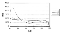
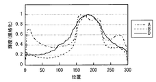
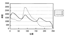
パターン密度は図61の線分aに示したようになっている
電圧:100Hz、140Vppのパルス電圧
光源:白色LED
(下側電極の辺部の凹凸形状)
輪郭:サイン2乗の関数
互いに隣り合う凹凸形状の間に形成される間隙の幅:0.1mm
凹凸形状に含まれる各凸部の幅:60mm
凹凸形状に含まれる各凸部のピッチ:1.9mm
(バックライト100)
導光板:厚み5mm、サイズ300×250mm、上面は平坦面
下側電極:ITO膜、幅83mm、3列
上側電極:ITO膜、幅75mm、4行、開口なし
電圧:100Hz、140Vppのパルス電圧
光源:白色LED
(バックライト1,2)
導光板:厚み5mm、サイズ300×250mm、上面に凸部あり
下側電極:ITO膜、幅83mm、3列
上側電極:ITO膜、幅75mm、4行、
100μm〜700μmの範囲内のサイズの複数の開口あり
単位面積当たりの開口の数は一定
開口の径が下側電極との対向部分ごとに、光源からの距離が遠くなるに
つれて小さくなっている
電圧:100Hz、140Vppのパルス電圧
光源:白色LED
導光板:厚み5mm、サイズ300×250mm、上面に凸部あり
下側電極:ITO膜、幅83mm、3列
輪郭がサイン2乗となるジグザグの凹凸形状あり
上側電極:ITO膜、幅75mm、4行、
100μm〜700μmの範囲内のサイズの複数の開口あり
単位面積当たりの開口の数は一定
開口の径が下側電極との対向部分ごとに、光源からの距離が遠くなるに
つれて小さくなっている
電圧:100Hz、140Vppのパルス電圧
光源:白色LED
導光板:厚み5mm、サイズ300×250mm、上面は平坦面
下側電極:ITO膜、幅83mm、3列
上側電極:ITO膜、幅75mm、4行、開口なし
電圧:100Hz、140Vppのパルス電圧
光源:白色LED
(下側電極)
3列
輪郭がサイン2乗となるジグザグの凹凸形状あり
互いに隣り合う凹凸形状の間に形成される間隙の幅:0.1mm
凹凸形状に含まれる各凸部の幅:30mm
凹凸形状に含まれる各凸部のピッチ:1.9mm
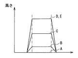
D1:0.862
D2:0.414
D1/D2:2.08
(上側電極)
4行
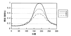
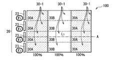
パターン密度が図75に示したようになっている
(凹凸形状と対向する領域内に、パターン密度が光源から離れるにつれて増大する
部分を意図的に5mmほど設けた)
(電圧のデューティ比)
光源寄りの部分電極:22%
中央の部分電極:40%
光源から最も離れた部分電極:100%
次に、上記各実施の形態のバックライト1,2の一適用例について説明する。
Claims (20)
- 導光板と、
前記導光板の側面に配置された光源と、
前記導光板の表面または内部に配置されると共に前記導光板と接着された光変調素子と を備え、
前記導光板は、当該導光板の側面のうち前記光源と対向する面の法線と平行な方向に延在する複数の凸部を有し、
前記光源は、互いに独立駆動可能な複数の光源ブロックからなり、
前記光変調素子は、
離間して互いに対向配置された一対の透明基板と、
前記一対の透明基板の一方の透明基板の表面に設けられ、かつ前記凸部の延在方向と交差する方向に延在する複数の第1電極と、
前記一対の透明基板の他方の透明基板の表面に設けられた第2電極と、
前記一対の透明基板の間隙に設けられ、かつ電場の大きさに応じて、前記光源からの光に対して散乱性もしくは透明性を示す光変調層と
を有する
照明装置。 - 各凸部の、当該凸部の延在方向と直交する方向の断面が、矩形状、台形状、または三角形状となっている
請求項1に記載の照明装置。 - 各凸部の高さは、前記光源に近い箇所で低く、前記光源から遠く離れた箇所で高くなっている
請求項1または請求項2に記載の照明装置。 - 各凸部の高さは、前記光源に最も近い箇所でゼロとなっている
請求項3に記載の照明装置。 - 各第1電極は、他の第1電極に隣接する辺部に、凹凸形状を有する
請求項1ないし請求項4のいずれか一項に記載の照明装置。 - 各第1電極は、複数の開口を有する
請求項5に記載の照明装置。 - 各第1電極は、凹凸形状を有する辺部を除いた部分に前記複数の開口を有する
請求項6に記載の照明装置。 - 各第1電極は、凹凸形状を有する辺部を除いた部分に電気的に接続された金属線を有する
請求項6または請求項7に記載の照明装置。 - 前記凹凸形状は、ジグザグ形状、波形状、台形状、ランプ形状またはランダム形状となっている
請求項5ないし請求項8のいずれか一項に記載の照明装置。 - 前記凹凸形状は、鋭角の先端を有する複数の凸部が配列されたジグザグ形状となっており、
各凸部の少なくとも1つの輪郭が、先端を原点側とする略サインm乗の関数(mは偶数)となっている
請求項9に記載の照明装置。 - 前記凹凸形状は、辺部に沿って配列された複数の凸部によって構成され、
互いに隣接する第1電極の辺部に形成されたそれぞれの複数の凸部は、互い違いに配置されている
請求項9に記載の照明装置。 - 前記第2電極は、単一のシート状電極からなり、
前記シート状電極は、パターニングされており、かつパターン密度が前記光源からの距離に応じて異なっている
請求項1ないし請求項11のいずれか一項に記載の照明装置。 - 前記第2電極は、複数の帯状電極からなり、
各帯状電極は、パターニングされており、かつパターン密度が帯状電極ごとに前記光源からの距離に応じて異なっている
請求項1ないし請求項11のいずれか一項に記載の照明装置。 - 前記第2電極は、単一のシート状電極または複数の帯状電極からなり、
前記第2電極は、パターニングされており、かつパターン密度が前記第1電極と対向する部分ごとに前記光源からの距離に応じて異なっている
請求項1ないし請求項11のいずれか一項に記載の照明装置。 - 各第1電極は、他の第1電極に隣接する辺部に、凹凸形状を有し、
前記第2電極は、単一のシート状電極または複数の帯状電極からなり、
前記第2電極は、パターニングされており、かつパターン密度が前記第1電極と対向する部分ごとに前記光源からの距離に応じて異なっており、
前記第2電極においてパターン密度が疎の箇所と密の箇所との境界が、当該第2電極のうち各第1電極の凹凸形状と対向する領域内に配置されている
請求項1ないし請求項11のいずれか一項に記載の照明装置。 - 各第1電極は、他の第1電極に隣接する辺部に、凹凸形状を有し、
前記第2電極は、単一のシート状電極または複数の帯状電極からなり、
前記第2電極は、パターニングされており、かつパターン密度が前記第1電極と対向する部分ごとに前記光源からの距離に応じて異なっており、
前記第2電極においてパターン密度が減少し始めた箇所から上昇し始めた箇所までの区間が、前記第1電極のうち互いに隣り合う2つの凹凸形状に含まれる凹部の底部で囲まれる区間と対向する範囲内に収まっている
請求項1ないし請求項11のいずれか一項に記載の照明装置。 - 前記第2電極は、複数の帯状電極からなり、
前記第2電極においてパターン密度が減少し始めた箇所でのパターン密度をD1とし、
前記第2電極においてパターン密度が上昇し始めた箇所でのパターン密度をD2とすると、D1,D2は以下の関係式を満たす
請求項16に記載の照明装置。
1<(D1/D2)<(互いに隣接する2つの帯状電極のうち相対的に前記光源寄りの帯状電極に掛かる電圧のデューティ比/(互いに隣接する2つの帯状電極のうち相対的に前記光源から離れた帯状電極に掛かる電圧のデューティ比) - 前記第2電極は、複数の開口を有し、
前記開口の径および密度の少なくとも一方が、前記光源からの距離に応じて異なっている
請求項12ないし請求項17のいずれか一項に記載の照明装置。 - マトリクス状に配置された複数の画素を有すると共に、前記複数の画素が映像信号に基づいて駆動される表示パネルと、
前記表示パネルを照明する照明装置と
を備え、
前記照明装置は、
導光板と、
前記導光板の側面に配置された光源と、
前記導光板の表面または内部に配置されると共に前記導光板と接着された光変調素子と
を有し、
前記導光板は、当該導光板の側面のうち前記光源と対向する面の法線と平行な方向に延在する複数の凸部を有し、
前記光源は、互いに独立駆動可能な複数の光源ブロックからなり、
前記光変調素子は、
離間して互いに対向配置された一対の透明基板と、
前記一対の透明基板の一方の透明基板の表面に設けられ、かつ前記凸部の延在方向と交差する方向に延在する複数の第1電極と、
前記一対の透明基板の他方の透明基板の表面に設けられた第2電極と、
前記一対の透明基板の間隙に設けられ、かつ電場の大きさに応じて、前記光源からの光に対して散乱性もしくは透明性を示す光変調層と
を有する
表示装置。 - 電圧印加対象の第1電極の前記光源からの距離と、前記映像信号とに応じて変調した電圧を各光源ブロックに印加する駆動回路をさらに備えた
請求項19に記載の表示装置。
Priority Applications (3)
| Application Number | Priority Date | Filing Date | Title |
|---|---|---|---|
| JP2010235925A JP5516319B2 (ja) | 2010-10-20 | 2010-10-20 | 照明装置および表示装置 |
| US13/271,805 US9069208B2 (en) | 2010-10-20 | 2011-10-12 | Edge source illumination device for liquid crystal display with patterned electrodes for light guide modulation layer |
| CN2011103106216A CN102537774A (zh) | 2010-10-20 | 2011-10-13 | 照明装置和显示装置 |
Applications Claiming Priority (1)
| Application Number | Priority Date | Filing Date | Title |
|---|---|---|---|
| JP2010235925A JP5516319B2 (ja) | 2010-10-20 | 2010-10-20 | 照明装置および表示装置 |
Publications (3)
| Publication Number | Publication Date |
|---|---|
| JP2012089385A JP2012089385A (ja) | 2012-05-10 |
| JP2012089385A5 JP2012089385A5 (ja) | 2013-10-31 |
| JP5516319B2 true JP5516319B2 (ja) | 2014-06-11 |
Family
ID=45972656
Family Applications (1)
| Application Number | Title | Priority Date | Filing Date |
|---|---|---|---|
| JP2010235925A Expired - Fee Related JP5516319B2 (ja) | 2010-10-20 | 2010-10-20 | 照明装置および表示装置 |
Country Status (3)
| Country | Link |
|---|---|
| US (1) | US9069208B2 (ja) |
| JP (1) | JP5516319B2 (ja) |
| CN (1) | CN102537774A (ja) |
Families Citing this family (39)
| Publication number | Priority date | Publication date | Assignee | Title |
|---|---|---|---|---|
| JP5699786B2 (ja) * | 2011-04-28 | 2015-04-15 | ソニー株式会社 | 表示装置および照明装置 |
| TW201400946A (zh) * | 2012-05-09 | 2014-01-01 | Sony Corp | 照明裝置及顯示裝置 |
| JP6035866B2 (ja) * | 2012-05-22 | 2016-11-30 | ソニー株式会社 | 照明装置および表示装置 |
| CN102692671B (zh) * | 2012-06-14 | 2016-02-24 | 深圳市华星光电技术有限公司 | 适用于3d显示的导光板 |
| US9091795B2 (en) * | 2012-06-14 | 2015-07-28 | Shenzhen China Star Optoelectronics Technology Co., Ltd. | Light guide plate for 3D displaying |
| US9684121B2 (en) * | 2012-07-27 | 2017-06-20 | Shenzhen China Star Optoelectronics Technology Co., Ltd | Side-edge backlight module having non-uniformly sized backlight sections and design method thereof |
| CN102767763B (zh) * | 2012-07-27 | 2014-06-25 | 深圳市华星光电技术有限公司 | 具有不均匀大小背光分区的侧入式背光模组及其设计方法 |
| JP6098064B2 (ja) * | 2012-08-08 | 2017-03-22 | ソニー株式会社 | 表示装置および照明装置 |
| TWI489335B (zh) * | 2012-08-09 | 2015-06-21 | Wistron Corp | 導電基板及觸控面板 |
| US11126040B2 (en) * | 2012-09-30 | 2021-09-21 | Optica Amuka (A.A.) Ltd. | Electrically-tunable lenses and lens systems |
| CN105026824B (zh) * | 2012-12-17 | 2017-10-31 | Lg伊诺特有限公司 | 后侧区域警报模块 |
| JP6171425B2 (ja) * | 2013-03-12 | 2017-08-02 | セイコーエプソン株式会社 | 虚像表示装置 |
| US10048429B2 (en) * | 2013-09-26 | 2018-08-14 | The Regents Of The University Of California | Illuminator with adjustable beam direction and divergence |
| CN103943033B (zh) * | 2014-04-02 | 2017-02-15 | 京东方科技集团股份有限公司 | 一种透明显示设备 |
| CA2947809C (en) | 2014-06-05 | 2023-03-28 | Optica Amuka (A.A.) Ltd. | Control of dynamic lenses |
| US9404632B2 (en) * | 2014-06-20 | 2016-08-02 | GM Global Technology Operations LLC | Lens assembly for a vehicle |
| JPWO2016017781A1 (ja) * | 2014-07-31 | 2017-04-27 | 日本ゼオン株式会社 | 有機el発光装置 |
| WO2016017734A1 (ja) * | 2014-07-31 | 2016-02-04 | 日本ゼオン株式会社 | 有機el発光装置 |
| JP2016057338A (ja) | 2014-09-05 | 2016-04-21 | 株式会社ジャパンディスプレイ | 表示装置及び光源装置 |
| JP6364335B2 (ja) | 2014-12-04 | 2018-07-25 | 株式会社ジャパンディスプレイ | 表示装置 |
| EP3040605B1 (en) * | 2015-01-02 | 2021-03-03 | Goodrich Lighting Systems GmbH | Light unit with an extended light emission surface |
| JP6671940B2 (ja) | 2015-12-07 | 2020-03-25 | 株式会社ジャパンディスプレイ | 表示装置 |
| US10466538B2 (en) | 2016-03-15 | 2019-11-05 | Japan Display Inc. | Display device |
| JP6716323B2 (ja) | 2016-04-01 | 2020-07-01 | 株式会社ジャパンディスプレイ | 表示装置 |
| WO2017182906A1 (en) | 2016-04-17 | 2017-10-26 | Optica Amuka (A.A.) Ltd. | Liquid crystal lens with enhanced electrical drive |
| JP2017215510A (ja) * | 2016-06-01 | 2017-12-07 | 株式会社ジャパンディスプレイ | 表示装置 |
| JP6800641B2 (ja) * | 2016-07-22 | 2020-12-16 | 株式会社ジャパンディスプレイ | 表示装置 |
| JP6720008B2 (ja) * | 2016-07-22 | 2020-07-08 | 株式会社ジャパンディスプレイ | 表示装置および表示装置の駆動方法 |
| JP6877910B2 (ja) | 2016-08-01 | 2021-05-26 | 株式会社ジャパンディスプレイ | 表示装置 |
| US11953764B2 (en) | 2017-07-10 | 2024-04-09 | Optica Amuka (A.A.) Ltd. | Tunable lenses with enhanced performance features |
| JP7005243B2 (ja) | 2017-09-14 | 2022-01-21 | 株式会社ジャパンディスプレイ | 表示装置 |
| KR102431685B1 (ko) * | 2017-11-24 | 2022-08-10 | 엘지디스플레이 주식회사 | 액정표시장치 |
| CN108267879B (zh) * | 2018-02-11 | 2021-02-02 | 京东方科技集团股份有限公司 | 一种液晶显示模组及显示设备 |
| CA3139811A1 (en) | 2019-06-02 | 2020-12-10 | Optica Amuka (A.A.) Ltd. | Electrically-tunable vision aid for treatment of myopia |
| CN111129088B (zh) * | 2019-12-17 | 2022-09-09 | 武汉华星光电半导体显示技术有限公司 | 有机发光二极管显示装置 |
| CN111350990B (zh) * | 2020-01-18 | 2022-03-25 | 深圳市强流明光电有限公司 | 可调性强的工矿灯 |
| JP2021136124A (ja) * | 2020-02-26 | 2021-09-13 | 株式会社ジャパンディスプレイ | 照明装置及び表示装置 |
| CN115494572A (zh) * | 2021-06-18 | 2022-12-20 | 华为技术有限公司 | 前光模组及显示装置 |
| US12099271B1 (en) * | 2023-07-19 | 2024-09-24 | Volkswagen Aktiengesellschaft | Controllable light propagation system |
Family Cites Families (27)
| Publication number | Priority date | Publication date | Assignee | Title |
|---|---|---|---|---|
| JPH06347790A (ja) | 1993-06-08 | 1994-12-22 | Fujitsu Ltd | 表示装置 |
| JP3187280B2 (ja) * | 1995-05-23 | 2001-07-11 | シャープ株式会社 | 面照明装置 |
| JP3257457B2 (ja) * | 1997-07-31 | 2002-02-18 | 株式会社日立製作所 | 液晶表示装置 |
| JPH11142843A (ja) | 1997-11-05 | 1999-05-28 | Toshiba Chem Corp | バックライト装置 |
| JP3324119B2 (ja) * | 1998-02-04 | 2002-09-17 | セイコーエプソン株式会社 | 液晶装置及び電子機器 |
| JPH11259007A (ja) * | 1998-03-10 | 1999-09-24 | Sony Corp | 反射型表示装置 |
| KR100679094B1 (ko) * | 1999-10-08 | 2007-02-05 | 엘지.필립스 엘시디 주식회사 | 백라이트 유닛 |
| JP4790937B2 (ja) * | 2001-07-09 | 2011-10-12 | ティーピーオー ホンコン ホールディング リミテッド | 反射電極を形成する方法及び液晶表示装置 |
| JP4436105B2 (ja) * | 2002-11-29 | 2010-03-24 | 富士通株式会社 | リフレクタ及び照明装置及び導光板及び表示装置 |
| JP2004206916A (ja) | 2002-12-24 | 2004-07-22 | Yoshihiro Sakai | 面状光源 |
| KR100493387B1 (ko) * | 2002-12-26 | 2005-06-07 | 엘지.필립스 엘시디 주식회사 | 표시장치의 백 라이트 유닛 및 그 백라이트 유닛을 사용한액정표시장치 |
| US7478942B2 (en) * | 2003-01-23 | 2009-01-20 | Samsung Electronics Co., Ltd. | Light guide plate with light reflection pattern |
| JP2004253335A (ja) | 2003-02-21 | 2004-09-09 | Kawaguchiko Seimitsu Co Ltd | バックライト装置 |
| JP2005301222A (ja) * | 2004-03-19 | 2005-10-27 | Sharp Corp | 表示装置 |
| JP4717494B2 (ja) * | 2004-05-20 | 2011-07-06 | セイコーインスツル株式会社 | 照明装置およびこれを用いた表示装置 |
| JP4647261B2 (ja) * | 2004-08-17 | 2011-03-09 | シチズンホールディングス株式会社 | 表示装置 |
| KR101114854B1 (ko) * | 2004-12-24 | 2012-03-07 | 엘지디스플레이 주식회사 | 배광장치 |
| KR20070043102A (ko) * | 2005-10-20 | 2007-04-25 | 삼성전자주식회사 | 점광원용 광 가이드 유닛, 이를 갖는 백라이트 어셈블리 및표시 장치 |
| CN2862089Y (zh) * | 2005-12-15 | 2007-01-24 | 比亚迪股份有限公司 | 一种导光板及背光模组 |
| JP4307477B2 (ja) * | 2006-07-04 | 2009-08-05 | 三星モバイルディスプレイ株式會社 | 導光板およびバックライトユニット |
| US7766528B2 (en) * | 2006-11-15 | 2010-08-03 | 3M Innovative Properties Company | Back-lit displays with high illumination uniformity |
| KR20080093617A (ko) * | 2007-04-17 | 2008-10-22 | 삼성전자주식회사 | 표시 장치 |
| KR101474244B1 (ko) * | 2008-01-11 | 2014-12-22 | 삼성디스플레이 주식회사 | 광학 시트 및 이의 제조 방법 |
| CN102150076A (zh) * | 2008-09-25 | 2011-08-10 | 夏普株式会社 | 光量调整装置、背光源单元、液晶显示面板和液晶显示装置 |
| JP5263593B2 (ja) * | 2008-10-07 | 2013-08-14 | ソニー株式会社 | 照明装置および表示装置 |
| US20110292096A1 (en) * | 2009-02-05 | 2011-12-01 | Sharp Kabushiki Kaisha | Liquid crystal display device |
| CN201487825U (zh) * | 2009-07-29 | 2010-05-26 | 比亚迪股份有限公司 | 一种导光膜及背光模组 |
-
2010
- 2010-10-20 JP JP2010235925A patent/JP5516319B2/ja not_active Expired - Fee Related
-
2011
- 2011-10-12 US US13/271,805 patent/US9069208B2/en not_active Expired - Fee Related
- 2011-10-13 CN CN2011103106216A patent/CN102537774A/zh active Pending
Also Published As
| Publication number | Publication date |
|---|---|
| JP2012089385A (ja) | 2012-05-10 |
| US9069208B2 (en) | 2015-06-30 |
| CN102537774A (zh) | 2012-07-04 |
| US20120098875A1 (en) | 2012-04-26 |
Similar Documents
| Publication | Publication Date | Title |
|---|---|---|
| JP5516319B2 (ja) | 照明装置および表示装置 | |
| JP5467388B2 (ja) | 照明装置および表示装置 | |
| JP5756931B2 (ja) | 照明装置および表示装置 | |
| JP5263593B2 (ja) | 照明装置および表示装置 | |
| JP6112108B2 (ja) | 照明装置および表示装置 | |
| JP5679308B2 (ja) | 照明装置および表示装置 | |
| JP5467389B2 (ja) | 照明装置および表示装置 | |
| JP4752911B2 (ja) | 照明装置、表示装置、およびエッジライト方式のバックライトに用いる光変調素子の製造方法 | |
| CN102686932B (zh) | 照明单元和显示器 | |
| JP2010157475A (ja) | 照明装置および表示装置 | |
| WO2012081497A1 (ja) | 照明装置、表示装置および3次元表示装置 | |
| WO2012153779A1 (ja) | 照明装置および表示装置 | |
| JP6035866B2 (ja) | 照明装置および表示装置 | |
| WO2012081498A1 (ja) | 照明装置および表示装置 |
Legal Events
| Date | Code | Title | Description |
|---|---|---|---|
| A521 | Request for written amendment filed |
Free format text: JAPANESE INTERMEDIATE CODE: A523 Effective date: 20130911 |
|
| A621 | Written request for application examination |
Free format text: JAPANESE INTERMEDIATE CODE: A621 Effective date: 20130911 |
|
| A977 | Report on retrieval |
Free format text: JAPANESE INTERMEDIATE CODE: A971007 Effective date: 20140221 |
|
| TRDD | Decision of grant or rejection written | ||
| A01 | Written decision to grant a patent or to grant a registration (utility model) |
Free format text: JAPANESE INTERMEDIATE CODE: A01 Effective date: 20140304 |
|
| A61 | First payment of annual fees (during grant procedure) |
Free format text: JAPANESE INTERMEDIATE CODE: A61 Effective date: 20140317 |
|
| R151 | Written notification of patent or utility model registration |
Ref document number: 5516319 Country of ref document: JP Free format text: JAPANESE INTERMEDIATE CODE: R151 |
|
| R250 | Receipt of annual fees |
Free format text: JAPANESE INTERMEDIATE CODE: R250 |
|
| R250 | Receipt of annual fees |
Free format text: JAPANESE INTERMEDIATE CODE: R250 |
|
| R250 | Receipt of annual fees |
Free format text: JAPANESE INTERMEDIATE CODE: R250 |
|
| R250 | Receipt of annual fees |
Free format text: JAPANESE INTERMEDIATE CODE: R250 |
|
| LAPS | Cancellation because of no payment of annual fees |