JP2017106962A - Display device - Google Patents
Display device Download PDFInfo
- Publication number
- JP2017106962A JP2017106962A JP2015238496A JP2015238496A JP2017106962A JP 2017106962 A JP2017106962 A JP 2017106962A JP 2015238496 A JP2015238496 A JP 2015238496A JP 2015238496 A JP2015238496 A JP 2015238496A JP 2017106962 A JP2017106962 A JP 2017106962A
- Authority
- JP
- Japan
- Prior art keywords
- light
- light modulation
- display
- display device
- electrode
- Prior art date
- Legal status (The legal status is an assumption and is not a legal conclusion. Google has not performed a legal analysis and makes no representation as to the accuracy of the status listed.)
- Granted
Links
Images


Classifications
-
- G—PHYSICS
- G02—OPTICS
- G02F—OPTICAL DEVICES OR ARRANGEMENTS FOR THE CONTROL OF LIGHT BY MODIFICATION OF THE OPTICAL PROPERTIES OF THE MEDIA OF THE ELEMENTS INVOLVED THEREIN; NON-LINEAR OPTICS; FREQUENCY-CHANGING OF LIGHT; OPTICAL LOGIC ELEMENTS; OPTICAL ANALOGUE/DIGITAL CONVERTERS
- G02F1/00—Devices or arrangements for the control of the intensity, colour, phase, polarisation or direction of light arriving from an independent light source, e.g. switching, gating or modulating; Non-linear optics
- G02F1/01—Devices or arrangements for the control of the intensity, colour, phase, polarisation or direction of light arriving from an independent light source, e.g. switching, gating or modulating; Non-linear optics for the control of the intensity, phase, polarisation or colour
- G02F1/13—Devices or arrangements for the control of the intensity, colour, phase, polarisation or direction of light arriving from an independent light source, e.g. switching, gating or modulating; Non-linear optics for the control of the intensity, phase, polarisation or colour based on liquid crystals, e.g. single liquid crystal display cells
- G02F1/133—Constructional arrangements; Operation of liquid crystal cells; Circuit arrangements
- G02F1/1333—Constructional arrangements; Manufacturing methods
- G02F1/1335—Structural association of cells with optical devices, e.g. polarisers or reflectors
- G02F1/1336—Illuminating devices
- G02F1/133615—Edge-illuminating devices, i.e. illuminating from the side
-
- G—PHYSICS
- G02—OPTICS
- G02F—OPTICAL DEVICES OR ARRANGEMENTS FOR THE CONTROL OF LIGHT BY MODIFICATION OF THE OPTICAL PROPERTIES OF THE MEDIA OF THE ELEMENTS INVOLVED THEREIN; NON-LINEAR OPTICS; FREQUENCY-CHANGING OF LIGHT; OPTICAL LOGIC ELEMENTS; OPTICAL ANALOGUE/DIGITAL CONVERTERS
- G02F1/00—Devices or arrangements for the control of the intensity, colour, phase, polarisation or direction of light arriving from an independent light source, e.g. switching, gating or modulating; Non-linear optics
- G02F1/01—Devices or arrangements for the control of the intensity, colour, phase, polarisation or direction of light arriving from an independent light source, e.g. switching, gating or modulating; Non-linear optics for the control of the intensity, phase, polarisation or colour
- G02F1/13—Devices or arrangements for the control of the intensity, colour, phase, polarisation or direction of light arriving from an independent light source, e.g. switching, gating or modulating; Non-linear optics for the control of the intensity, phase, polarisation or colour based on liquid crystals, e.g. single liquid crystal display cells
- G02F1/133—Constructional arrangements; Operation of liquid crystal cells; Circuit arrangements
- G02F1/1333—Constructional arrangements; Manufacturing methods
- G02F1/1334—Constructional arrangements; Manufacturing methods based on polymer dispersed liquid crystals, e.g. microencapsulated liquid crystals
-
- G—PHYSICS
- G02—OPTICS
- G02F—OPTICAL DEVICES OR ARRANGEMENTS FOR THE CONTROL OF LIGHT BY MODIFICATION OF THE OPTICAL PROPERTIES OF THE MEDIA OF THE ELEMENTS INVOLVED THEREIN; NON-LINEAR OPTICS; FREQUENCY-CHANGING OF LIGHT; OPTICAL LOGIC ELEMENTS; OPTICAL ANALOGUE/DIGITAL CONVERTERS
- G02F1/00—Devices or arrangements for the control of the intensity, colour, phase, polarisation or direction of light arriving from an independent light source, e.g. switching, gating or modulating; Non-linear optics
- G02F1/01—Devices or arrangements for the control of the intensity, colour, phase, polarisation or direction of light arriving from an independent light source, e.g. switching, gating or modulating; Non-linear optics for the control of the intensity, phase, polarisation or colour
- G02F1/13—Devices or arrangements for the control of the intensity, colour, phase, polarisation or direction of light arriving from an independent light source, e.g. switching, gating or modulating; Non-linear optics for the control of the intensity, phase, polarisation or colour based on liquid crystals, e.g. single liquid crystal display cells
- G02F1/133—Constructional arrangements; Operation of liquid crystal cells; Circuit arrangements
- G02F1/1333—Constructional arrangements; Manufacturing methods
- G02F1/1335—Structural association of cells with optical devices, e.g. polarisers or reflectors
- G02F1/133509—Filters, e.g. light shielding masks
-
- G—PHYSICS
- G02—OPTICS
- G02F—OPTICAL DEVICES OR ARRANGEMENTS FOR THE CONTROL OF LIGHT BY MODIFICATION OF THE OPTICAL PROPERTIES OF THE MEDIA OF THE ELEMENTS INVOLVED THEREIN; NON-LINEAR OPTICS; FREQUENCY-CHANGING OF LIGHT; OPTICAL LOGIC ELEMENTS; OPTICAL ANALOGUE/DIGITAL CONVERTERS
- G02F1/00—Devices or arrangements for the control of the intensity, colour, phase, polarisation or direction of light arriving from an independent light source, e.g. switching, gating or modulating; Non-linear optics
- G02F1/01—Devices or arrangements for the control of the intensity, colour, phase, polarisation or direction of light arriving from an independent light source, e.g. switching, gating or modulating; Non-linear optics for the control of the intensity, phase, polarisation or colour
- G02F1/13—Devices or arrangements for the control of the intensity, colour, phase, polarisation or direction of light arriving from an independent light source, e.g. switching, gating or modulating; Non-linear optics for the control of the intensity, phase, polarisation or colour based on liquid crystals, e.g. single liquid crystal display cells
- G02F1/133—Constructional arrangements; Operation of liquid crystal cells; Circuit arrangements
- G02F1/1333—Constructional arrangements; Manufacturing methods
- G02F1/1335—Structural association of cells with optical devices, e.g. polarisers or reflectors
- G02F1/133553—Reflecting elements
-
- G—PHYSICS
- G02—OPTICS
- G02F—OPTICAL DEVICES OR ARRANGEMENTS FOR THE CONTROL OF LIGHT BY MODIFICATION OF THE OPTICAL PROPERTIES OF THE MEDIA OF THE ELEMENTS INVOLVED THEREIN; NON-LINEAR OPTICS; FREQUENCY-CHANGING OF LIGHT; OPTICAL LOGIC ELEMENTS; OPTICAL ANALOGUE/DIGITAL CONVERTERS
- G02F1/00—Devices or arrangements for the control of the intensity, colour, phase, polarisation or direction of light arriving from an independent light source, e.g. switching, gating or modulating; Non-linear optics
- G02F1/01—Devices or arrangements for the control of the intensity, colour, phase, polarisation or direction of light arriving from an independent light source, e.g. switching, gating or modulating; Non-linear optics for the control of the intensity, phase, polarisation or colour
- G02F1/13—Devices or arrangements for the control of the intensity, colour, phase, polarisation or direction of light arriving from an independent light source, e.g. switching, gating or modulating; Non-linear optics for the control of the intensity, phase, polarisation or colour based on liquid crystals, e.g. single liquid crystal display cells
- G02F1/133—Constructional arrangements; Operation of liquid crystal cells; Circuit arrangements
- G02F1/1333—Constructional arrangements; Manufacturing methods
- G02F1/1337—Surface-induced orientation of the liquid crystal molecules, e.g. by alignment layers
-
- G—PHYSICS
- G02—OPTICS
- G02F—OPTICAL DEVICES OR ARRANGEMENTS FOR THE CONTROL OF LIGHT BY MODIFICATION OF THE OPTICAL PROPERTIES OF THE MEDIA OF THE ELEMENTS INVOLVED THEREIN; NON-LINEAR OPTICS; FREQUENCY-CHANGING OF LIGHT; OPTICAL LOGIC ELEMENTS; OPTICAL ANALOGUE/DIGITAL CONVERTERS
- G02F1/00—Devices or arrangements for the control of the intensity, colour, phase, polarisation or direction of light arriving from an independent light source, e.g. switching, gating or modulating; Non-linear optics
- G02F1/01—Devices or arrangements for the control of the intensity, colour, phase, polarisation or direction of light arriving from an independent light source, e.g. switching, gating or modulating; Non-linear optics for the control of the intensity, phase, polarisation or colour
- G02F1/13—Devices or arrangements for the control of the intensity, colour, phase, polarisation or direction of light arriving from an independent light source, e.g. switching, gating or modulating; Non-linear optics for the control of the intensity, phase, polarisation or colour based on liquid crystals, e.g. single liquid crystal display cells
- G02F1/133—Constructional arrangements; Operation of liquid crystal cells; Circuit arrangements
- G02F1/1333—Constructional arrangements; Manufacturing methods
- G02F1/1343—Electrodes
- G02F1/134309—Electrodes characterised by their geometrical arrangement
-
- G—PHYSICS
- G02—OPTICS
- G02F—OPTICAL DEVICES OR ARRANGEMENTS FOR THE CONTROL OF LIGHT BY MODIFICATION OF THE OPTICAL PROPERTIES OF THE MEDIA OF THE ELEMENTS INVOLVED THEREIN; NON-LINEAR OPTICS; FREQUENCY-CHANGING OF LIGHT; OPTICAL LOGIC ELEMENTS; OPTICAL ANALOGUE/DIGITAL CONVERTERS
- G02F1/00—Devices or arrangements for the control of the intensity, colour, phase, polarisation or direction of light arriving from an independent light source, e.g. switching, gating or modulating; Non-linear optics
- G02F1/01—Devices or arrangements for the control of the intensity, colour, phase, polarisation or direction of light arriving from an independent light source, e.g. switching, gating or modulating; Non-linear optics for the control of the intensity, phase, polarisation or colour
- G02F1/13—Devices or arrangements for the control of the intensity, colour, phase, polarisation or direction of light arriving from an independent light source, e.g. switching, gating or modulating; Non-linear optics for the control of the intensity, phase, polarisation or colour based on liquid crystals, e.g. single liquid crystal display cells
- G02F1/137—Devices or arrangements for the control of the intensity, colour, phase, polarisation or direction of light arriving from an independent light source, e.g. switching, gating or modulating; Non-linear optics for the control of the intensity, phase, polarisation or colour based on liquid crystals, e.g. single liquid crystal display cells characterised by the electro-optical or magneto-optical effect, e.g. field-induced phase transition, orientation effect, guest-host interaction or dynamic scattering
-
- G—PHYSICS
- G02—OPTICS
- G02F—OPTICAL DEVICES OR ARRANGEMENTS FOR THE CONTROL OF LIGHT BY MODIFICATION OF THE OPTICAL PROPERTIES OF THE MEDIA OF THE ELEMENTS INVOLVED THEREIN; NON-LINEAR OPTICS; FREQUENCY-CHANGING OF LIGHT; OPTICAL LOGIC ELEMENTS; OPTICAL ANALOGUE/DIGITAL CONVERTERS
- G02F1/00—Devices or arrangements for the control of the intensity, colour, phase, polarisation or direction of light arriving from an independent light source, e.g. switching, gating or modulating; Non-linear optics
- G02F1/01—Devices or arrangements for the control of the intensity, colour, phase, polarisation or direction of light arriving from an independent light source, e.g. switching, gating or modulating; Non-linear optics for the control of the intensity, phase, polarisation or colour
- G02F1/13—Devices or arrangements for the control of the intensity, colour, phase, polarisation or direction of light arriving from an independent light source, e.g. switching, gating or modulating; Non-linear optics for the control of the intensity, phase, polarisation or colour based on liquid crystals, e.g. single liquid crystal display cells
- G02F1/133—Constructional arrangements; Operation of liquid crystal cells; Circuit arrangements
- G02F1/1333—Constructional arrangements; Manufacturing methods
- G02F1/1334—Constructional arrangements; Manufacturing methods based on polymer dispersed liquid crystals, e.g. microencapsulated liquid crystals
- G02F1/13347—Constructional arrangements; Manufacturing methods based on polymer dispersed liquid crystals, e.g. microencapsulated liquid crystals working in reverse mode, i.e. clear in the off-state and scattering in the on-state
-
- G—PHYSICS
- G02—OPTICS
- G02F—OPTICAL DEVICES OR ARRANGEMENTS FOR THE CONTROL OF LIGHT BY MODIFICATION OF THE OPTICAL PROPERTIES OF THE MEDIA OF THE ELEMENTS INVOLVED THEREIN; NON-LINEAR OPTICS; FREQUENCY-CHANGING OF LIGHT; OPTICAL LOGIC ELEMENTS; OPTICAL ANALOGUE/DIGITAL CONVERTERS
- G02F1/00—Devices or arrangements for the control of the intensity, colour, phase, polarisation or direction of light arriving from an independent light source, e.g. switching, gating or modulating; Non-linear optics
- G02F1/01—Devices or arrangements for the control of the intensity, colour, phase, polarisation or direction of light arriving from an independent light source, e.g. switching, gating or modulating; Non-linear optics for the control of the intensity, phase, polarisation or colour
- G02F1/13—Devices or arrangements for the control of the intensity, colour, phase, polarisation or direction of light arriving from an independent light source, e.g. switching, gating or modulating; Non-linear optics for the control of the intensity, phase, polarisation or colour based on liquid crystals, e.g. single liquid crystal display cells
- G02F1/133—Constructional arrangements; Operation of liquid crystal cells; Circuit arrangements
- G02F1/1333—Constructional arrangements; Manufacturing methods
- G02F1/1335—Structural association of cells with optical devices, e.g. polarisers or reflectors
- G02F1/1336—Illuminating devices
- G02F1/133616—Front illuminating devices
-
- G—PHYSICS
- G02—OPTICS
- G02F—OPTICAL DEVICES OR ARRANGEMENTS FOR THE CONTROL OF LIGHT BY MODIFICATION OF THE OPTICAL PROPERTIES OF THE MEDIA OF THE ELEMENTS INVOLVED THEREIN; NON-LINEAR OPTICS; FREQUENCY-CHANGING OF LIGHT; OPTICAL LOGIC ELEMENTS; OPTICAL ANALOGUE/DIGITAL CONVERTERS
- G02F1/00—Devices or arrangements for the control of the intensity, colour, phase, polarisation or direction of light arriving from an independent light source, e.g. switching, gating or modulating; Non-linear optics
- G02F1/01—Devices or arrangements for the control of the intensity, colour, phase, polarisation or direction of light arriving from an independent light source, e.g. switching, gating or modulating; Non-linear optics for the control of the intensity, phase, polarisation or colour
- G02F1/13—Devices or arrangements for the control of the intensity, colour, phase, polarisation or direction of light arriving from an independent light source, e.g. switching, gating or modulating; Non-linear optics for the control of the intensity, phase, polarisation or colour based on liquid crystals, e.g. single liquid crystal display cells
- G02F1/133—Constructional arrangements; Operation of liquid crystal cells; Circuit arrangements
- G02F1/1333—Constructional arrangements; Manufacturing methods
- G02F1/1337—Surface-induced orientation of the liquid crystal molecules, e.g. by alignment layers
- G02F1/133738—Surface-induced orientation of the liquid crystal molecules, e.g. by alignment layers for homogeneous alignment
-
- G—PHYSICS
- G02—OPTICS
- G02F—OPTICAL DEVICES OR ARRANGEMENTS FOR THE CONTROL OF LIGHT BY MODIFICATION OF THE OPTICAL PROPERTIES OF THE MEDIA OF THE ELEMENTS INVOLVED THEREIN; NON-LINEAR OPTICS; FREQUENCY-CHANGING OF LIGHT; OPTICAL LOGIC ELEMENTS; OPTICAL ANALOGUE/DIGITAL CONVERTERS
- G02F1/00—Devices or arrangements for the control of the intensity, colour, phase, polarisation or direction of light arriving from an independent light source, e.g. switching, gating or modulating; Non-linear optics
- G02F1/01—Devices or arrangements for the control of the intensity, colour, phase, polarisation or direction of light arriving from an independent light source, e.g. switching, gating or modulating; Non-linear optics for the control of the intensity, phase, polarisation or colour
- G02F1/13—Devices or arrangements for the control of the intensity, colour, phase, polarisation or direction of light arriving from an independent light source, e.g. switching, gating or modulating; Non-linear optics for the control of the intensity, phase, polarisation or colour based on liquid crystals, e.g. single liquid crystal display cells
- G02F1/137—Devices or arrangements for the control of the intensity, colour, phase, polarisation or direction of light arriving from an independent light source, e.g. switching, gating or modulating; Non-linear optics for the control of the intensity, phase, polarisation or colour based on liquid crystals, e.g. single liquid crystal display cells characterised by the electro-optical or magneto-optical effect, e.g. field-induced phase transition, orientation effect, guest-host interaction or dynamic scattering
- G02F1/13756—Devices or arrangements for the control of the intensity, colour, phase, polarisation or direction of light arriving from an independent light source, e.g. switching, gating or modulating; Non-linear optics for the control of the intensity, phase, polarisation or colour based on liquid crystals, e.g. single liquid crystal display cells characterised by the electro-optical or magneto-optical effect, e.g. field-induced phase transition, orientation effect, guest-host interaction or dynamic scattering the liquid crystal selectively assuming a light-scattering state
Landscapes
- Physics & Mathematics (AREA)
- Nonlinear Science (AREA)
- Chemical & Material Sciences (AREA)
- Crystallography & Structural Chemistry (AREA)
- General Physics & Mathematics (AREA)
- Optics & Photonics (AREA)
- Mathematical Physics (AREA)
- Spectroscopy & Molecular Physics (AREA)
- Geometry (AREA)
- Dispersion Chemistry (AREA)
- Liquid Crystal (AREA)
- Planar Illumination Modules (AREA)
Abstract
【課題】表示品位の向上が可能な表示装置を提供する。
【解決手段】表示面を有し、前記表示面に入射する光を選択的に反射させて画像を表示する表示パネルと、前記表示パネルの表示面側に配置されその主面内に複数の部分を有する光変調素子と、前記光変調素子の側面に配置された光源と、を備え、前記光源から前記光変調素子に入射した光で前記部分毎に所定輝度で前記表示パネルを照明する照明装置と、を備えた表示装置。
【選択図】図2A display device capable of improving display quality is provided.
A display panel having a display surface and selectively reflecting light incident on the display surface to display an image, and a plurality of portions arranged on the display surface side of the display panel in the main surface And a light source disposed on a side surface of the light modulation element, and illuminates the display panel with a predetermined luminance for each portion with light incident on the light modulation element from the light source And a display device.
[Selection] Figure 2
Description
本発明の実施形態は、表示装置に関する。 Embodiments described herein relate generally to a display device.
外光の反射率を制御して画像を表示する反射型表示装置は、画像の輝度が不足する場合が多いため、補助照明手段として照明装置(フロントライト)を備える構成が適用可能である。従来の反射型表示装置は、表示する画像に関わらず、フロントライトを全面発光するため、消費電力の増加やコントラストの悪化が生じる恐れがある。 A reflective display device that displays an image by controlling the reflectance of external light often lacks the brightness of the image. Therefore, a configuration including an illuminating device (front light) as an auxiliary illumination unit is applicable. Since the conventional reflective display device emits the entire front light regardless of the image to be displayed, there is a risk of increased power consumption and poor contrast.
本実施形態の目的は、表示品位の向上が可能な表示装置を提供することにある。 An object of the present embodiment is to provide a display device capable of improving display quality.
本実施形態によれば、
表示面を有し、前記表示面に入射する光を選択的に反射させて画像を表示する表示パネルと、前記表示パネルの表示面側に配置されその主面内に複数の部分を有する光変調素子と、前記光変調素子の側面に配置された光源と、を備え、前記光源から前記光変調素子に入射した光で前記部分毎に所定輝度で前記表示パネルを照明する照明装置と、を備えた表示装置が提供される。
According to this embodiment,
A display panel having a display surface and selectively reflecting light incident on the display surface to display an image; and a light modulation disposed on the display surface side of the display panel and having a plurality of portions in the main surface An illumination device that illuminates the display panel with a predetermined brightness for each of the portions with light incident on the light modulation element from the light source, and a light source disposed on a side surface of the light modulation element A display device is provided.
本実施形態によれば、
表示面を有し、前記表示面に入射する光を選択的に反射させて画像を表示する表示パネルと、前記表示パネルの表示面側に配置された光変調素子と、前記光変調素子の側面に配置された光源と、を備え、前記光源から前記光変調素子に入射した光で前記表示パネルを照明する照明装置と、を備え、前記光変調素子は、前記表示パネルに近接する側に配置された第1透明基板と、前記表示パネルから離れる側に配置された第2透明基板と、前記第1および第2透明基板の間に位置する光変調層と、前記光変調層に対して電場を印加するための第1電極および第2電極と、を備え、前記光変調層は、前記第1および第2電極によって生じる電場の大きさおよび向きに応じて前記光源からの光に対して全体的もしくは部分的に散乱性もしくは透明性を示す、表示装置が提供される。
According to this embodiment,
A display panel having a display surface and selectively reflecting light incident on the display surface to display an image; a light modulation element disposed on a display surface side of the display panel; and a side surface of the light modulation element A lighting device that illuminates the display panel with light incident on the light modulation element from the light source, and the light modulation element is disposed on a side close to the display panel A first transparent substrate formed, a second transparent substrate disposed on a side away from the display panel, a light modulation layer positioned between the first and second transparent substrates, and an electric field with respect to the light modulation layer A first electrode and a second electrode for applying the light, and the light modulation layer is entirely applied to the light from the light source according to the magnitude and direction of the electric field generated by the first and second electrodes. Or partially scattering or transparent Shown, the display device is provided.
以下、本実施形態について、図面を参照しながら説明する。なお、開示はあくまで一例に過ぎず、当業者において、発明の主旨を保っての適宜変更について容易に想到し得るものについては、当然に本発明の範囲に含有されるものである。また、図面は、説明をより明確にするため、実際の態様に比べて、各部の幅、厚さ、形状等について模式的に表される場合があるが、あくまで一例であって、本発明の解釈を限定するものではない。また、本明細書と各図において、既出の図に関して前述したものと同一又は類似した機能を発揮する構成要素には同一の参照符号を付し、重複する詳細な説明を適宜省略することがある。 Hereinafter, the present embodiment will be described with reference to the drawings. It should be noted that the disclosure is merely an example, and those skilled in the art can easily conceive of appropriate changes while maintaining the gist of the invention are naturally included in the scope of the present invention. In addition, for the sake of clarity, the drawings may be schematically represented with respect to the width, thickness, shape, etc. of each part as compared to actual aspects, but are merely examples, and The interpretation is not limited. In addition, in the present specification and each drawing, components that perform the same or similar functions as those described above with reference to the previous drawings are denoted by the same reference numerals, and repeated detailed description may be omitted as appropriate. .
図1は、本実施形態に係る表示装置の構成例の断面を示す図である。
表示装置1は、照明装置10、表示パネルPNL、および、照明装置10と表示パネルPNLとを駆動する駆動回路50を備えている。表示装置1は、表示パネルPNLの表示面側に照明装置10を備え、表示面に入射する光を選択的に反射させて画像を表示する、いわゆる反射型表示装置である。
FIG. 1 is a diagram illustrating a cross-section of a configuration example of a display device according to the present embodiment.
The display device 1 includes a
照明装置10は、光源20と、光変調素子30とを備えている。光源20は、光変調素子30の側面に配置されている。光変調素子30は、表示パネルPNLに対向配置されている。光変調素子30は、表示パネルPNLから離間しており、例えば空気層を介して表示パネルPNLと対向している。光変調素子30は、表示パネルPNLに対応した形状、例えば、上面、下面および側面で囲まれた直方体状となっている。なお、以下では、光変調素子30の側面のうち光源20からの光が入射する側面を光入射面30Aと称するものとし、表示パネルPNLの表示面と対向し光が出射される下面を光照射面30Bと称するものとする。
The
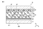
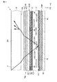
図2は、図1に図示した光変調素子の断面を示す図である。
光変調素子30は、透明基板31、下側電極32、配向膜33、光変調層34、配向膜35、上側電極36、および透明基板37を順に備えている。
FIG. 2 is a view showing a cross section of the light modulation element shown in FIG.
The
一対の透明基板31、37のうち透明基板31は、下側電極32が配置された面とは反対側に光照射面30Bを有しており、図1に図示した表示パネルPNLに近接する側に配置されている。対して、透明基板37は、表示パネルPNLから離れる側に配置されている。透明基板31、37は、離間して互いに対向配置されている。透明基板31、37は、光変調層34を支持するものであり、一般に、可視光に対して透明な基板、例えば、ガラス板や、プラスチックフィルムによって構成されている。
Of the pair of
一対の電極32、36のうち下側電極32は、透明基板31の光変調層34側の表面上に配置されたものであり、例えば、面内全体に渡って形成された単一のシート状の電極である。上側電極36は、透明基板37の光変調層34側の表面上に配置されたものであり、図示した断面の例では、開口部APを有し面内方向で不連続に形成されている。上側電極36は、例えば、透明基板37側に配置された光吸収層36−2と、光吸収層36−2の透明基板31に近接する側に配置された反射層36−1と、を備えている。
下側電極32は、例えば、酸化インジウムスズ(ITO;Indium Tin Oxide)や、酸化インジウム亜鉛(IZO;Indium Zinc Oxide)などの透明な導電性材料からなる。透明な導電性材料は、可能な限り可視光の吸収が小さい材料であることが好ましい。反射層36−1は、光反射性を有し、光変調層34側から上側電極36へ入射する光を反射する。反射層36−1は、例えばアルミニウムやチタンなどの金属材料によって構成されている。光吸収層36−2は、可視光を吸収する光吸収性を有し、透明基板37側から上側電極36へ入射する光(外光)を反射する。光吸収層36−2は、例えば黒色樹脂によって構成されている。反射層36−1および光吸収層36−2は、少なくとも一方が導電性を備えている。なお、上側電極36は、光吸収層36−2が導電性を有している場合、反射層36−1を省略することができる。
The
The
図示した上側電極36は、図示しない領域で連続しており、互いに同電位となる。光変調素子30を光変調素子30の法線方向から見たときに、上側電極36のうち連続な部分と対向する箇所の光変調素子30が光変調セル30−1を構成している。上記の連続な部分は、図4に後述する部分電極36Aに相当し、1つの光変調セル30−1は、光変調素子30の1つの部分電極36Aと対向する部分に相当する。光変調セル30−1は、下側電極32および部分電極36Aに所定の電圧を印加することにより別個独立に駆動することの可能な部位であり、下側電極32および部分電極36Aに印加される電圧値の大きさに応じて、光源20からの光に対して透明性を示したり、散乱性を示したりする。なお、透明性、散乱性については、光変調層34を説明する際に詳細に説明する。
The
配向膜33,35は、電極32,36と光変調層34との間に配置され、例えば、光変調層34に用いられる液晶やモノマーを配向させるものである。配向膜の種類としては、例えば、垂直配向膜および水平配向膜があるが、図示した構成例では、配向膜33,35には水平配向膜が用いられる。水平配向膜としては、例えば、ポリイミド、ポリアミドイミドなどの樹脂膜を配向処理することにより形成された配向膜が挙げられる。配向処理は、例えばラビング処理や光配向処理などである。透明基板31,36としてプラスチックフィルムを用いる場合には、透明基板31,36の変形を抑制する観点から、製造工程において、透明基板31,36の表面に配向膜33,35を塗布した後の焼成温度ができるだけ低いことが好ましい。このため、配向膜33,35として、100℃以下の温度で形成可能なポリアミドイミドを用いることが好ましい。
The
また、垂直、水平いずれの配向膜においても、液晶とモノマーを配向させる機能があれば十分である。また、配向膜33,35を用いなくても、例えば、下側電極32および上側電極36間に電場や磁場を印加することによっても、光変調層34に用いられる液晶やモノマーを配向させることが可能である。つまり、下側電極32および上側電極36間に電場や磁場を印加させながら、紫外線を照射してモノマーを重合することで、電圧印加状態での液晶やモノマーの配向状態を固定させることができる。液晶やモノマーの配向に電圧を用いる場合には、配向用と駆動用とで別々の電極を形成するか、液晶材料に周波数によって誘電率異方性の符号が反転する二周波液晶などを用いることができる。また、液晶やモノマーの配向に磁場を用いる場合、液晶やモノマーとして磁化率異方性の大きい材料を用いることが好ましく、例えば、ベンゼン環の多い材料を用いることが好ましい。
In addition, in any of the vertical and horizontal alignment films, a function of aligning the liquid crystal and the monomer is sufficient. Further, without using the
光変調層34は、一対の透明基板31,37の間に配置されている。光変調層34は、電極32,36によって生じる電場の大きさや向きに応じて、光源20からの光に対して全体的もしくは部分的に散乱性もしくは透明性を示すものである。具体的には、光変調層34は、下側電極32および上側電極36に電圧が印加されていない時に光源20からの光に対して透明性を示し、下側電極32および上側電極36に電圧が印加されている時に光源20からの光に対して散乱性を示すものである。光変調層34は、例えば、バルク34Aと、バルク34A内に分散された微粒子状の複数の微粒子34Bとを含んだ複合層となっている。バルク34Aおよび微粒子34Bは光学異方性を有している。微粒子34Bは第1領域に相当し、バルク34Aは第2領域に相当する。
The
バルク34Aおよび微粒子34Bは、電場に対する応答速度が互いに異なっている。バルク34Aは、例えば、電場に対して応答しない筋状構造もしくは多孔質構造となっているか、または微粒子34Bの応答速度よりも遅い応答速度を有する筋状構造もしくは棒状構造となっている。バルク34Aは、例えば、低分子モノマーを重合化することにより得られた高分子材料によって構成されている。バルク34Aは、例えば、配向膜33,35の配向方向に沿って配向した、配向性および重合性を有する材料(例えばモノマー)を熱および光の少なくとも一方によって重合させることにより形成されている。
The
一方、微粒子34Bは、例えば、液晶材料を主に含んで構成されており、バルク34Aの応答速度よりも十分に早い応答速度を有している。微粒子34B内に含まれる液晶材料(液晶分子)は、例えば棒状分子である。微粒子34B内に含まれる液晶分子として、正の誘電率異方性を有するもの(いわゆるポジ型液晶)を用いることが好ましい。バルク34Aが筋状構造または棒状構造となっている場合、微粒子34Bの液晶分子は、例えばバルク34Aの筋状構造または棒状構造の長軸方向(配向方向)と平行に配向する。
On the other hand, the
上記した、バルク34Aを形成する配向性および重合性を有するモノマーとしては、光学的に異方性を有しており、かつ液晶と複合する材料であればよいが、本実施の形態では紫外線で硬化する低分子モノマーであることが好ましい。電圧無印加の状態で、液晶材料と、低分子モノマーを重合化することにより形成されたもの(高分子材料)との光学的異方性の方向が一致していることが好ましいので、紫外線硬化前において、液晶材料と低分子モノマーが同一方向に配向していることが好ましい。微粒子34Bとして液晶材料が用いられる場合に、その液晶材料が棒状分子であるときには、使用するモノマー材料の形状も棒状であることが好ましい。以上のことから、モノマー材料としては重合性と液晶性を併せ持つ材料を用いることが好ましく、例えば、重合性官能基として、アクリレート基、メタクリレート基、アクリロイルオキシ基、メタクリロイルオキシ基、ビニルエーテル基およびエポキシ基からなる群から選ばれた少なくとも1つの官能基を有することが好ましい。これらの官能基は、紫外線、赤外線または電子線を照射したり、加熱したりすることによって重合させることができる。紫外線照射時の配向度低下を抑制するために、多官能基をもつ液晶性材料を添加することもできる。バルク34Aを上述した筋状構造とする場合には、バルク34Aの原料として、2官能液晶性モノマーを用いることが好ましい。また、バルク34Aの原料に対して、液晶性を示す温度の調整を目的に単官能モノマーを添加したり、架橋密度向上を目的に3官能以上のモノマーを添加したりすることもできる。
As the above-mentioned monomer having the orientation and polymerizability for forming the
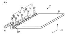
図3は、図1に図示した照明装置の構成を示す図である。
光源20は、例えば、複数の点状光源23を第2方向Yに一列に配置して構成されている。各点状光源23は、光入射面30Aに向かって光を射出するようになっており、例えば、光入射面30Aとの対向面に発光スポットを有する発光素子からなる。そのような発光素子としては、例えば、LED、または、レーザダイオード(LD;Laser Diode)などが挙げられる。
FIG. 3 is a diagram illustrating a configuration of the illumination device illustrated in FIG. 1.
The
複数の点状光源23は、例えば、2個以上の点状光源23ごとに、共通の基板24上に配置されていてもよい。この場合、1つの基板24と、その基板24上に配置された複数の点状光源23とにより、光源ブロック25が構成されている。基板24は、例えば、点状光源23と駆動回路50とを電気的に接続する配線が形成された回路基板であり、各点状光源23は、この回路基板上に実装されている。共通の基板24上に配置された各点状光源23(光源ブロック25内の各点状光源23)は、駆動回路50によって一括で(非独立に)駆動されるようになっており、例えば、図示しないが、互いに並列に、または互いに直列に、接続されている。また、互いに異なる基板24上に配置された点状光源23(各光源ブロック25内の点状光源23)は、例えば、駆動回路50によって互いに独立に駆動されるようになっており、例えば、互いに異なる電流経路に接続されている。互いに異なる基板24上に設けられた点状光源23(各光源ブロック25内の点状光源23)は、例えば、図示しないが、互いに並列または直列に接続されており、例えば、駆動回路50によって一括で(非独立に)駆動されるようになっていてもよい。光源20は、光変調素子30の1つの側面にだけ設けられていてもよいし、光変調素子30の2つの側面(例えば互いに対向する2つの側面)に設けられていてもよい。
The plurality of point
図4は、図2に図示した電極の構成を示す図である。
上側電極36は、例えば、複数の帯状の部分電極36Aを互いに並列配置したものである。部分電極36Aは、例えば、第2方向Y、すなわち光入射面30Aと平行な方向に延在し、第1方向X、すなわち光入射面30Aと直交する方向に配列されている。各部分電極36Aは、互いに電気的に分離されており、個別独立に電圧を印加される。なお、複数の部分電極36Aは、互いに電気的に接続されていてもよい。一方、下側電極32は、例えば、光変調層34を介して複数の部分電極36Aと第3方向Zで対向するシート状の電極である。
上側電極36および下側電極32の形状は、特に限定されるものではなく、例えば、下側電極32は、並列配置された複数の部分電極で構成されていてもよい。なお、図示を省略するが、光変調層34に電場を形成する一対の電極は、両方とも光変調層34の同じ側に配置されていてもよい。このような一対の電極は、例えば、第1方向Xまたは第2方向Yに交互に配列され、光変調層34にX−Y平面と平行な横電場を形成する。
FIG. 4 is a diagram illustrating a configuration of the electrode illustrated in FIG. 2.
The
The shapes of the
図5は、図4に図示した上側電極の構成を示す図である。
部分電極36Aは、複数の開口部APを備えている。開口部APは、図示した例では四角形状となっているが、特に限定されるものではなく、円形状、楕円形状、または多角形状となっていてもよい。開口部APの密度(部分電極36Aのうち単位面積当たりの開口部APの占有率)は、例えば各部分電極36Aにおいて等しいが、各部分電極36Aにおいて異なっていてもよい。開口部APの密度は、開口部APの径および数を変化させることで、制御される。なお、開口部APの密度は、部分電極36Aのパターン密度(部分電極36Aのうち単位面積当たりの開口部AP以外の部分の占有率)より高いことが望ましい。そうすることで、表示装置1は、表示パネルPNLに表示された画像の、光変調素子30における透過率を向上させることができる。
FIG. 5 is a diagram illustrating a configuration of the upper electrode illustrated in FIG. 4.
The
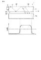
図6は、電圧が印加されていない状態の光変調層を模式的に示す図である。
図6は、下側電極32および部分電極36A間に電圧が印加されていない場合の、バルク34Aおよび微粒子34B内の配向状態の一例を模式的に表したものである。
FIG. 6 is a diagram schematically showing the light modulation layer in a state where no voltage is applied.
FIG. 6 schematically shows an example of the orientation state in the
楕円体134Aは、下側電極32および部分電極36A間に電圧が印加されていない時の、バルク34Aの屈折率異方性を示す屈折率楕円体の一例を表したものである。楕円体134Bは、下側電極32および部分電極36A間に電圧が印加されていない時の、微粒子34Bの屈折率異方性を示す屈折率楕円体の一例を表したものである。この屈折率楕円体は、様々な方向から入射した直線偏光の屈折率をテンソル楕円体で表したものであり、光が入射する方向からの楕円体の断面を見ることによって、幾何的に屈折率を知ることができるものである。
The
バルク34Aおよび微粒子34Bは、例えば、下側電極32および上側電極36間に電圧が印加されていない時に、バルク34Aの光学軸AX1(具体的には楕円体134Aの長軸)および微粒子34Bの光学軸AX2(具体的には楕円体134Bの長軸)の向きが互いに一致する(平行となる)構成となっている。なお、光学軸AX1,AX2とは、偏光方向によらず屈折率が1つの値になるような光線の進行方向と平行な線を指している。また、下側電極32および上側電極36間に電圧が印加されていない時に、光学軸AX1および光学軸AX2の向きは常に互いに一致している必要はなく、光学軸AX1の向きと光学軸AX2の向きとが、例えば製造誤差などによって多少ずれていてもよい。
For example, when no voltage is applied between the
図7は、図6に図示した状態の光変調層の平面および断面を示す図である。
下側電極32および部分電極36A間に電圧が印加されていない時に、光学軸AX2は、光変調素子30の光入射面30Aと平行(またはほぼ平行)となると共に、光照射面30Bと平行(またはほぼ平行)となっている。つまり、下側電極32および上側電極36間に電圧が印加されていない時に、光学軸AX2は、部分電極32Aまたは上側電極36を含む面と平行(またはほぼ平行)となっており、かつ部分電極32Aの延在方向と平行(またはほぼ平行)となっている。
FIG. 7 is a diagram illustrating a plane and a cross section of the light modulation layer in the state illustrated in FIG. 6.
When no voltage is applied between the
一方、光学軸AX1は、光変調素子30の光入射面30Aと平行(またはほぼ平行)となると共に、光照射面30Bと平行(またはほぼ平行)となっている。つまり、下側電極32および部分電極36A間に電圧が印加されていない時に、光学軸AX1は、光学軸AX2と平行(またはほぼ平行)となっている。
On the other hand, the optical axis AX1 is parallel (or substantially parallel) to the
ここで、バルク34Aおよび微粒子34Bの常光屈折率が互いに等しく、かつバルク34Aおよび微粒子34Bの異常光屈折率が互いに等しいことが好ましい。この場合に、例えば、部分電極32Aおよび上側電極36間に電圧が印加されていない時には、正面方向および斜め方向を含むあらゆる方向において屈折率差がほとんどなく、高い透明性が得られる。これにより、例えば、正面方向に向かう光および斜め方向に向かう光は、光変調層34内で散乱されることなく、光変調層34を透過する。
Here, it is preferable that the ordinary light refractive indexes of the
図8は、電圧が印加されている状態の光変調層を模式的に示す図である。
図8は、下側電極32および部分電極36A間に電圧が印加されている時の、バルク34Aおよび微粒子34B内の配向状態の一例を模式的に表したものである。
FIG. 8 is a diagram schematically showing the light modulation layer in a state where a voltage is applied.
FIG. 8 schematically shows an example of the orientation state in the
楕円体134Aは、下側電極32および部分電極36A間に電圧が印加されている時の、バルク34Aの屈折率異方性を示す屈折率楕円体の一例を表したものである。楕円体134Bは、下側電極32および部分電極36A間に電圧が印加されている時の、微粒子34Bの屈折率異方性を示す屈折率楕円体の一例を表したものである。
The
また、バルク34Aおよび微粒子34Bは、例えば、下側電極32および部分電極36A間に電圧が印加されている時には、光学軸AX1および光学軸AX2の向きが互いに異なる(交差もしくは直交する)構成となっている。
Further, the
図9は、図8に図示した状態の光変調層の平面および断面を示す図である。
微粒子34Bは、例えば、下側電極32および部分電極36A間に電圧が印加されている時に、光学軸AX2が光変調素子30の光入射面30Aと平行(もしくはほぼ平行)となると共に光照射面30Bの法線と平行(もしくはほぼ平行)となる構成となっている。つまり、下側電極32および部分電極36A間に電圧が印加されている時に、光学軸AX2は、下側電極32または部分電極36Aを含む面と直交(もしくはほぼ直交)している。
FIG. 9 is a diagram illustrating a plane and a cross section of the light modulation layer in the state illustrated in FIG. 8.
For example, when a voltage is applied between the
一方、バルク34Aは、下側電極32および部分電極36A間への電圧印加の有無に拘らず、光学軸AX1が一定となる構成となっている。すなわち、光学軸AX1は、光入射面30Aと平行(またはほぼ平行)となると共に、光照射面30Bと平行(またはほぼ平行)となっている。つまり、下側電極32および部分電極36A間に電圧が印加されている時に、光学軸AX1は、光学軸AX2と直交(またはほぼ直交)となっている。
On the other hand, the
したがって、下側電極32および部分電極36A間に電圧が印加されている時には、光変調層34において、バルク34Aおよび微粒子34Bの間で屈折率差が生じ、散乱性が得られる。これにより、例えば、正面方向に向かう光および斜め方向に向かう光は、光変調層34内で散乱される。
Therefore, when a voltage is applied between the
このように、微粒子34B内の液晶分子は電圧の印加、無印加に応じて上述したような変化を示すが、この変化の過程で、バルク34Aは電圧変化に対して応答せず、バルク34Aの筋状構造の長軸方向は、配向膜33,35の配向処理方向AL(光入射面30Aと平行な方向)を向いている。そのため、下側電極32および上側電極36間に電圧が印加されている時には、光源20から出力され、光変調層34内を伝播する光は、バルク34Aの筋状構造の短軸方向の平均的な筋状組織サイズの周期で、微粒子34Bの異常光屈折率とバルク34Aの常光屈折率との差を感じながら伝播する。その結果、光変調層34内を伝播する光は、光変調層34の厚さ方向に大きく散乱し、光入射面30Aと平行な方向にはあまり散乱しない。つまり、光変調層34は、光源20から出力され、光変調層34内を伝播する光に対して異方性散乱を示す。
As described above, the liquid crystal molecules in the
なお、バルク34Aの屈折率差(=異常光屈折率−常光屈折率)や、微粒子34Bの屈折率差(=異常光屈折率−常光屈折率)は、できるだけ大きいことが好ましく、0.05以上であることが好ましく、0.1以上であることがより好ましく、0.15以上であることがさらに好ましい。バルク34Aおよび微粒子34Bの屈折率差が大きい場合には、光変調層34の散乱能が高くなり、導光条件を容易に破壊することができ、光変調素子30からの光を取り出しやすいからである。
The refractive index difference (= extraordinary refractive index-ordinary refractive index) of the
図10は、光変調素子における光の挙動を示す図である。
光源20からの光L1(斜め方向からの光)は、光変調素子30内で透明となった透過部分30Tにおいて、界面(透明基板31,37と空気との界面)において全反射され、光変調素子30内を導光される。この結果、透過部分30Tの光照射面30Bの輝度は、光変調素子30が光変調層34を備えていない導光板である場合(図中の一点鎖線)と比べて下がる。
FIG. 10 is a diagram illustrating the behavior of light in the light modulation element.
Light L1 from the light source 20 (light from an oblique direction) is totally reflected at the interface (interface between the
光L1は、光変調素子30内で散乱状態となった散乱部分30Sにおいて光入射面30Aと平行な方向に散乱される。光照射面30B側に散乱された光は、界面(透明基板31と空気との界面)を透過し、上側電極36側に散乱された光は、反射層36−1で光照射面30B側へ反射される。従って、散乱部分30Sの光照射面30Bの輝度は、光変調素子30が光変調層34を備えていない導光板である場合(図8中の一点鎖線)と比べて極めて高くなり、しかも、透過部分30Tの輝度が低下した分だけ、部分的な白表示の輝度(輝度突き上げ)が大きくなる。
The light L1 is scattered in a direction parallel to the
照明装置10は、部分電極36Aに対向する領域である光変調セル30−1ごとに透過部分30Tと散乱部分30Sとを切り替えることができる。すなわち、照明装置10は、光変調素子30の主面内に複数の部分を有し、この部分ごとに所定輝度で表示パネルPNLを照明する。
The illuminating
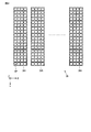
図11は、高明度部分を局所的に照明する場合の照明装置の動作を示す図である。
本構成例において、照明装置10は、光源ブロック25および光変調素子30により、光照射面30Bから出射する光の輝度分布を2次元で調整することが可能なローカルディミングを実現することができる。このようなローカルディミングの利用例について説明する。
FIG. 11 is a diagram illustrating the operation of the illumination device when locally illuminating the high brightness portion.
In this configuration example, the
図示した例では、照明装置10は、光変調素子30の照明可能な照明領域Aに、サブエリアSB1乃至SB6を有している。サブエリアSB1乃至SB6は、それぞれ光変調セル30−1に対応する領域であり、個別独立に透過部分30Tと散乱部分30Sとを切り替えることができる。照明領域Aに対応する領域に表示される画像に周囲よりも明度が高い高明度部分HBが含まれる場合、この高明度部分HBに対応する位置を高輝度で照明するように、各光源ブロック25および光変調素子30を制御する。
図示した例においては、高明度部分HBの第1方向Xにおける位置に対応した光源ブロック25が点灯(オン)され、他の光源ブロック25が消灯(オフ)されている。これにより、光変調素子30内の点灯した光源ブロック25に対応する領域には光が導光され、他の領域には光が導光されない。さらに、高明度部分HBの第2方向Yにおける位置に対応したサブエリアSB3,SB4,SB5が図10で上述した散乱部分30Sとなり、他のサブエリアSB1,SB2,SB6が図10で上述した透過部分30Tとなるように、光変調素子30が制御される。すなわち、光変調素子30は、照明領域Aにおいて光が導光されている領域の部分ごとに光の散乱強度を変更する。これにより、照明装置10から出射される光は、高明度部分HBの近辺において輝度が高く、他の部分において輝度が低くなる。
図示した例において、高明度部分HBと重なる面積が最も大きいサブエリアSB4が第1散乱強度I1となり、サブエリアSB4よりも高明度部分HBと重なる面積が小さいサブエリアSB3,SB5が第1散乱強度I1よりも低い第2散乱強度I2(I1>I2)となり、高明度部分HBと重ならないサブエリアSB1,SB2,SB6が第2散乱強度I2よりも低い第3散乱強度I3(I2>I3)となるように光変調素子30が制御されている。図11においては、ハッチングの種類によりこれらの散乱強度を表している。このように、サブエリアSBの散乱強度を多段階で制御することで、より細やかに表示画像のコントラストを調整することができる。
In the illustrated example, the
In the illustrated example, the
In the illustrated example, the sub-area SB4 having the largest area overlapping with the high-lightness portion HB is the first scattering intensity I1, and the sub-areas SB3 and SB5 having smaller areas overlapping with the high-lightness portion HB than the sub-area SB4 are the first scattering intensity. The second scattering intensity I2 (I1> I2) is lower than I1, and the third scattering intensity I3 (I2> I3) in which the sub-areas SB1, SB2, SB6 that do not overlap the high brightness portion HB are lower than the second scattering intensity I2 Thus, the
図12は、表示パネルの構成例の断面を示す図である。ここでは、説明に必要な構成のみを図示している。
表示パネルPNLは、第1基板SUB1、第2基板SUB2、液晶層LC、および、光学素子ODを備えている。第2基板SUB2は、第1基板SUB1と対向配置されており、第1基板SUB1よりも光変調素子30に近接する側に配置されている。
FIG. 12 is a diagram illustrating a cross section of a configuration example of the display panel. Here, only the configuration necessary for the description is illustrated.
The display panel PNL includes a first substrate SUB1, a second substrate SUB2, a liquid crystal layer LC, and an optical element OD. The second substrate SUB2 is disposed to face the first substrate SUB1, and is disposed closer to the
第1基板SUB1は、第1絶縁基板100、画素電極PE、第1配向膜AL1などを備えている。図示しないが、第1基板SUB1は、各種配線に加えて、画素電極PEへの電圧の印加を制御するスイッチング素子などを備えている。画素電極PEは、第1絶縁基板100の第2基板SUB2と対向する側に位置している。画素電極PEは、反射電極に相当し、アルミニウムや銀などの光反射性を有する金属材料によって形成された反射層を含んでいる。第1配向膜AL1は、画素電極PEを覆っている。
The first substrate SUB1 includes a first insulating
第2基板SUB2は、第2絶縁基板200、遮光層BM、カラーフィルタ層CF、オーバーコート層OC、共通電極CE、第2配向膜AL2などを備えている。
遮光層BMは、第2絶縁基板200の第1基板SUB1と対向する側に位置している。図示した例では、遮光層BMは、隣り合う画素電極PEの隙間に対向している。カラーフィルタ層CFは、第2絶縁基板200の第1基板SUB1と対向する側に位置し、それらの一部が遮光層BMと重なっている。カラーフィルタ層CFは、詳述しないが、例えば、赤色カラーフィルタ、緑色カラーフィルタ、および、青色カラーフィルタを含んでいる。赤色カラーフィルタは、赤色を表示する画素に配置される。緑色カラーフィルタは、緑色を表示する画素に配置される。青色カラーフィルタは、青色を表示する画素に配置される。なお、カラーフィルタ層CFは、白色などの他の色のカラーフィルタ、あるいは、透明層を含んでいても良い。
The second substrate SUB2 includes a second insulating
The light shielding layer BM is located on the side of the second insulating
オーバーコート層OCは、カラーフィルタ層CFを覆っている。共通電極CEは、オーバーコート層OCの第1基板SUB1と対向する側に位置している。共通電極CEは、複数の画素電極PEと対向している。共通電極CEは、ITOやIZOなどの透明導電材料によって形成されている。第2配向膜AL2は、共通電極CEを覆っている。 The overcoat layer OC covers the color filter layer CF. The common electrode CE is located on the side of the overcoat layer OC that faces the first substrate SUB1. The common electrode CE is opposed to the plurality of pixel electrodes PE. The common electrode CE is formed of a transparent conductive material such as ITO or IZO. The second alignment film AL2 covers the common electrode CE.
なお、第2基板SUB2において、互いに異なる色を表示する画素の境界においては、異なる色の複数のカラーフィルタが積層されることで、透過率を低減することができるため、遮光層BMを省略しても良い。モノクロ表示タイプの表示パネルPNLにおいては、カラーフィルタ層CFは省略することができる。 In the second substrate SUB2, the light shielding layer BM is omitted because the transmittance can be reduced by laminating a plurality of color filters of different colors at the boundary of pixels displaying different colors. May be. In the monochrome display type display panel PNL, the color filter layer CF can be omitted.
液晶層LCは、第1基板SUB1と第2基板SUB2との間に保持され、第1配向膜AL1と第2配向膜AL2との間に位置した液晶分子LMを含んでいる。液晶分子LMは、第1配向膜AL1および第2配向膜AL2の配向規制力により、所定の方向へ初期配向している。 The liquid crystal layer LC is held between the first substrate SUB1 and the second substrate SUB2, and includes liquid crystal molecules LM located between the first alignment film AL1 and the second alignment film AL2. The liquid crystal molecules LM are initially aligned in a predetermined direction by the alignment regulating force of the first alignment film AL1 and the second alignment film AL2.
光学素子ODは、第2基板SUB2の光変調素子30に近接する側に配置されている。光学素子ODは、例えば、位相差板RT、偏光板PLなどを備えている。位相差板RTは、1/4波長板としての機能を有している。一例では、位相差板RTは、1/4波長板と1/2波長板とを積層した積層体であり、波長依存性を低減し、カラー表示に利用される波長範囲において所望の位相差が得られるように構成されている。偏光板PLの透過軸は、バルク34Aの筋状構造の長軸と平行な方向に延在している。すなわち、偏光板PLの透過軸は、第2方向Yに延在している。
The optical element OD is disposed on the side close to the
次に、図示した反射型液晶表示装置の動作について説明する。なお、オン状態とは、画素電極PEおよび共通電極CEに電圧が印加された状態であり、オフ状態とは、画素電極PEおよび共通電極CEに電圧が印加されていない状態であるものとする。
光変調素子30内を導光された光L1は、散乱部分30Sで散乱され、光照射面30Bから出射される。偏光板PLの透過軸とバルク34Aの筋状構造の長軸とが互いに平行である場合、光変調層34で散乱された光L1は、偏光板PLの透過軸と平行な方向に偏光している。光照射面30Bから出射された光L1は、偏光板PLを透過する際に偏光度が向上して直線偏光となる。その後、光L1は、位相差板RTを透過する際に円偏光となる。第2基板SUB2を透過する際にカラーフィルタ層CFで着色された光L1は、液晶層LQを透過して画素電極PEで反射され、第2基板SUB2へ向かう。例えば、表示パネルPNLは、オフ状態の時に液晶層LQを透過する光L1の位相を変化させず、オン状態の時に液晶層LQを透過する光L1の位相を変化させる。オフ状態の場合、画素電極PEで反射された光L1は、位相差板RTを透過する際に偏光板PLの透過軸と直交する方向に偏光した直線偏光となり、偏光板PLを透過しない。オン状態の場合、画素電極PEで反射された光L1は、液晶層LQで位相が変化しているため、位相差板RTを透過しても偏光板PLの透過軸と直交する方向に偏光しておらず、偏光板PLを透過する。なお、画素電極PEで反射された光L1は、拡散範囲の拡大、虹色の防止などの目的のために散乱されることが望ましい。例えば、光学素子ODに散乱層が配置され、画素電極PEで反射された光L1は、散乱層によって散乱されてもよい。一方で、図示したように、光L1は、散乱部分30Sで散乱されるため、光学素子ODは、散乱層を備えていなくてもよい。なお、光学素子ODの構成は、図示した例に限らす、他の光学機能層を備えていてもよい。
Next, the operation of the illustrated reflective liquid crystal display device will be described. The on state is a state in which a voltage is applied to the pixel electrode PE and the common electrode CE, and the off state is a state in which no voltage is applied to the pixel electrode PE and the common electrode CE.
The light L1 guided through the
本実施形態によれば、表示装置1は、反射型の表示パネルPNLと、表示パネルPNLの表示面側に配置された照明装置10とを備えている。照明装置10は、光変調素子30と、光変調素子30の側面に配置され光変調素子30の内部へ光L1を出射する光源20と、を備えている。照明装置10は、光変調素子30に、電極32,36に印加される電圧に応じて散乱性もしくは透過性を示す光変調層34を備え、光変調素子30から表示パネルへ出射される光の輝度を部分ごとに変更する。このため、表示装置1は、一様な輝度分布の光が表示パネルPNLに入射する場合に比べ、高明度部分HBとその周囲とのコントラストを高めることができる。従って、本実施形態によれば、表示品位の向上が可能な表示装置1を提供することができる。
According to the present embodiment, the display device 1 includes the reflective display panel PNL and the
照明装置10は、複数の光源ブロック25および複数の光変調セル30−1(サブエリアSB)を備えている。光源ブロック25は、第2方向Yに並んでいる。光変調セル30−1は、第2方向Yに延在し第1方向Xに並んでいる部分電極36Aに対応する領域である。光源20に備えられた光源ブロック25が全て一括で駆動される場合、照明装置10は、光変調セル30−1の散乱性を制御することで、光照射面30Bから出射される光L1の輝度分布を調整する1次元ローカルディミングが可能となる。一方、光源20に備えられた光源ブロック25が個別独立に駆動される場合、交差する方向に並ぶ光源ブロック25および光変調セル30−1を制御することで、2次元ローカルディミングが可能となる。すなわち、照明装置10は、1次元ローカルディミングに比べて、よりピンポイントで高明度部分HBを照明することが可能となり、表示装置1のコントラストを高めることができる。また、全ての光源ブロック25を常時点灯させるのではなく、表示に必要なものを点灯させ他を消灯させることができるので、表示装置1の消費電力を低減することが可能となる。
The
光変調層34は、液晶材料を含む第1領域(微粒子34B)と、高分子材料を含む第2領域(バルク34A)とで構成されている。オフ状態のとき、第1領域の光学軸AX2は、第2領域の光学軸AX1と平行である。第1領域および第2領域の屈折率楕円体134A,134Bが同じ形状をしているため、光変調層34は、オフ状態で透明性を示し、オン状態で散乱性を示す。例えば、表示装置1が画像を表示するのに充分な外光が存在しない場合に照明装置10を補助的に点灯する。照明装置10の点灯が必要でない場合はオフ状態を維持し、必要な場合だけ電極32,36に電圧を印加してオン状態にすればいいので、表示装置1の消費電力を低減することができる。
The
光変調素子30の上側電極36は、光吸収層36−2と、光吸収層36−2よりも第1透明基板31に近接する側に配置された反射層36−1と、を備えている。光吸収層36−2は、反射層36−1における外光の反射を抑制することができるため、表示装置1は、外光反射のぎらつきによる表示品位の低下を抑制することができる。また、反射層36−1は、光変調層34において散乱された光のうち、表示パネルPNLとは反対の方向へ散乱された光を表示パネルPNLの方向へ反射することができ、光源20から出射された光L1の利用効率を向上させることができる。すなわち、表示装置1は、消費電力を低減することができる。
The
オフ状態の場合、光学軸AX1,AX2は、光源20から光変調素子30への光L1の入射面と平行であり、電極32,36と光変調層34との間に配置された水平配向膜33,35の配向規制力によって光照射面30Bと平行である。電極32,36は、光変調層34を介して対向しており第1領域の液晶材料がポジ型液晶分子であるため、オフ状態の場合、光学軸AX2は、光変調層34の主面(XY平面)に垂直な厚さ方向に延在する。オン状態の光変調層34の散乱異方性は、光変調層34の主面に垂直な厚さ方向の散乱が、光変調層34の主面に平行な方向の散乱よりも大きいため、光源20から出射された光L1は、散乱部分30Sで効率的に表示パネルPNLの方向へ散乱されることができ、表示装置1は、消費電力を低減することができる。
In the off state, the optical axes AX1 and AX2 are parallel to the incident surface of the light L1 from the
第2領域は、第2方向Yに長軸を有する筋状構造となっている。このとき、散乱部分30Sでは、筋状構造の長軸と平行な方向に偏光した光が散乱される。このため、光源20から出射される光L1が第2方向Yに偏光している場合、散乱部分30Sにおける散乱強度を向上させることができる。また、表示パネルPNLに配置された偏光板PLの透過軸が筋状構造の長軸と平行である場合、偏光板PLにおける光の損失を低減することができる。
The second region has a streak structure having a long axis in the second direction Y. At this time, in the
次に本実施形態における電極32,36の構成の変形例について説明する。なお、このような変形例においても、上記した構成例と同様の効果を得ることができる。
Next, a modified example of the configuration of the
図13は、電極の構成の第1変形例を示す図である。
本変形例は、下側電極32が複数の部分電極32Aを有している点で、図4に図示した構成例と相違している。
FIG. 13 is a diagram illustrating a first modification of the electrode configuration.
This modification is different from the configuration example illustrated in FIG. 4 in that the
部分電極32Aは、部分電極36Aと対向している。部分電極32Aは、光入射面30Aの延在方向である第2方向Yに延在し、光入射面30Aと直交する第1方向Xに並んでいる。部分電極32A,36Aは、それぞれ駆動回路38に接続されている。駆動回路38は、部分電極32A,36Aへの印加電圧を制御している。このような変形例においては、下側電極32が面内全体に渡って形成された単一のシート状の電極である場合と比べて光変調素子30の透過率を向上させることができ、表示装置1の表示品位を向上させることができる。
The
図14は、電極の構成の第2変形例を示す図である。
本変形例は、部分電極32A,36Aが第2方向Yで不連続に形成されている点で、図13に図示した変形例と相違している。
FIG. 14 is a diagram illustrating a second modification of the configuration of the electrodes.
This modification is different from the modification shown in FIG. 13 in that the
部分電極32A,36Aは、島状に形成され、互いに対向している。また、部分電極32A,36Aは、第1方向Xおよび第2方向Yにマトリクス状に配置されている。全ての部分電極32A,36Aは、駆動回路38に接続されている。このような変形例においては、光源20の複数の点光源が一括駆動であったとしても、部分電極32A,36Aへの印加電圧の制御のみで2次元ローカルディミングを実現することができる。また、照明が必要な高明度部分HBに対応する部分電極32A,36Aにだけ電圧を印加することができるため、消費電力を低減することができる。さらに、光変調素子30の主面に対する電極32,36の面積が占める割合を低下させることで、光変調素子30の透過率を向上させることができ、表示装置1の表示品位を向上させることができる。
The
図15は、電極の構成の第3変形例を示す図である。
本変形例は、部分電極32Aの配列方向が図13に図示した変形例と相違している。
FIG. 15 is a diagram illustrating a third modification of the electrode configuration.
This modification is different from the modification shown in FIG. 13 in the arrangement direction of the
部分電極32Aは、第1方向Xに延在し、第2方向Yに並んでいる。部分電極32Aと部分電極36Aとは、それぞれ互いに交差している。本変形例においては、電圧が印加された部分電極32Aおよび36Aの対向している交差点においてのみ光を散乱させることができるため、光源20の複数の点光源が一括駆動であったとしても、部分電極32A,36Aへの印加電圧の制御のみで2次元ローカルディミングを実現することができる。
The
次に、本実施形態における上側電極36の構成の変形例について説明する。
Next, a modified example of the configuration of the
図16は、上側電極の構成の第1変形例を示す図である。
本変形例は、開口部APが円形状である点で、図5に図示した構成例と相違している。
FIG. 16 is a diagram illustrating a first modification of the configuration of the upper electrode.
This modification is different from the configuration example illustrated in FIG. 5 in that the opening AP is circular.
開口部APは、それぞれの部分電極36Aに形成されている。図示した例において、各部分電極36Aにおける開口部APの数および大きさは等しく、開口部APの密度(部分電極36Aのうち単位面積当たりの開口部APの占有率)は、各部分電極36Aにおいて等しい。このような変形例においても、上記した構成例と同様の効果を得ることができる。
The opening AP is formed in each
図17は、上側電極の構成の第2変形例を示す図である。
本変形例は、開口部APの密度が第1方向Xで異なっている点で、図16に図示した変形例と相違している。
FIG. 17 is a diagram illustrating a second modification of the configuration of the upper electrode.
This modification is different from the modification illustrated in FIG. 16 in that the density of the opening AP is different in the first direction X.
開口部APの密度は、光源20に近い部分電極36Aにおいては密となり、光源20から離れた部分電極36Aにおいては疎となっている。図示した例では、開口部APの数は、各部分電極36Aにおいて等しい。開口部APの径は、光源20から離れるにつれ小さくなっている。なお、開口部APの密度は、開口部APの数によって制御されていてもよい。すなわち、開口部APの数は、光源20から離れるにつれ少なくなっていてもよい。このような変形例においても、図16に図示した変形例と同様に、上記した構成例と同様の効果を得ることができる。さらに、このような変形例においては、光量の強い光源20の近くの領域と光量の弱い光源20から離れた領域とで光変調素子30から出射される光の輝度を平均化することができるため、輝度ムラによる表示品位の低下を抑制することができる。
The density of the opening AP is dense in the
次に、本実施形態における光変調素子30の構成の変形例について説明する。
Next, a modified example of the configuration of the
図18は、光変調素子の構成の変形例を示す図である。
本変形例は、光変調層34が高透過部分34C(第3領域)を備えている点で、図2に図示した構成例と相違している。
FIG. 18 is a diagram illustrating a modification of the configuration of the light modulation element.
This modification is different from the configuration example illustrated in FIG. 2 in that the
高透過部分34Cは、バルク34Aおよび微粒子34Bよりも光透過率が高く、例えば樹脂材料で形成されている。高透過部分34Cは、隣接する光変調セル30−1に配置されたバルク34Aおよび微粒子34Bの間に配置され、例えば透明基板37の透明基板31に近接する側の面に配置されている。高透過部分34Cは、例えば透明基板37と一体に形成されていてもよい。高透過部分34Cは、配向膜35で覆われ、配向膜35を介して配向膜33と接触している。このような変形例においても、上記した構成例と同様の効果を得ることができる。さらに、光変調層34の透過率が向上し、表示装置1の表示品位を向上させることができる。
The
以上説明したように、本実施形態によれば、表示品位の向上が可能な表示装置を提供することができる。 As described above, according to this embodiment, it is possible to provide a display device capable of improving display quality.
なお、本発明のいくつかの実施形態を説明したが、これらの実施形態は、例として提示したものであり、発明の範囲を限定することは意図していない。これらの新規な実施形態は、その他の様々な形態で実施されることが可能であり、発明の要旨を逸脱しない範囲で、種々の省略、置き換え、変更を行うことができる。これらの実施形態やその変形は、発明の範囲や要旨に含まれるとともに、特許請求の範囲に記載された発明とその均等の範囲に含まれる。 In addition, although some embodiment of this invention was described, these embodiment is shown as an example and is not intending limiting the range of invention. These novel embodiments can be implemented in various other forms, and various omissions, replacements, and changes can be made without departing from the spirit of the invention. These embodiments and modifications thereof are included in the scope and gist of the invention, and are included in the invention described in the claims and the equivalents thereof.
1…表示装置 10…照明装置 20…光源 30…光変調素子 30B…光照射面
30−1…光変調セル 31,37…透明基板 33,35…配向膜
32…下側電極 36…上側電極 36−1…反射層 36−2…光吸収層
34…光変調層 34A…バルク 34B…微粒子
DESCRIPTION OF SYMBOLS 1 ...
30-1 ...
32 ...
34 ...
Claims (15)
前記表示パネルの表示面側に配置されその主面内に複数の部分を有する光変調素子と、前記光変調素子の側面に配置された光源と、を備え、前記光源から前記光変調素子に入射した光で前記部分毎に所定輝度で前記表示パネルを照明する照明装置と、
を備えた表示装置。 A display panel having a display surface and selectively reflecting light incident on the display surface to display an image;
A light modulation element disposed on a display surface side of the display panel and having a plurality of portions in a main surface thereof; and a light source disposed on a side surface of the light modulation element, and is incident on the light modulation element from the light source An illuminating device that illuminates the display panel at a predetermined brightness for each of the portions with the obtained light;
A display device comprising:
前記表示パネルに近接する側に配置された第1透明基板と、
前記表示パネルから離れる側に配置された第2透明基板と、
前記第1および第2透明基板の間に位置する光変調層と、
前記光変調層に対して電場を印加するための第1電極および第2電極と、を備え、
前記光変調層は、前記第1および第2電極によって生じる電場の大きさおよび向きに応じて前記光源からの光に対して全体的もしくは部分的に散乱性もしくは透明性を示す、請求項1に記載の表示装置。 The light modulation element is
A first transparent substrate disposed on a side close to the display panel;
A second transparent substrate disposed on the side away from the display panel;
A light modulation layer located between the first and second transparent substrates;
A first electrode and a second electrode for applying an electric field to the light modulation layer,
2. The light modulation layer according to claim 1, wherein the light modulation layer is totally or partially scatterable or transparent with respect to light from the light source depending on a magnitude and direction of an electric field generated by the first and second electrodes. The display device described.
前記光源は、第1方向に交差する第2方向に並んだ複数の点状光源を備えた、請求項3に記載の表示装置。 The partial electrodes are arranged in the first direction,
The display device according to claim 3, wherein the light source includes a plurality of point light sources arranged in a second direction intersecting the first direction.
前記光変調層で散乱された光は、前記偏光板の透過軸と平行な方向に偏光している、請求項2に記載の表示装置。 The display panel includes a polarizing plate disposed on a side close to the lighting device,
The display device according to claim 2, wherein the light scattered by the light modulation layer is polarized in a direction parallel to a transmission axis of the polarizing plate.
前記表示パネルの表示面側に配置された光変調素子と、前記光変調素子の側面に配置された光源と、を備え、前記光源から前記光変調素子に入射した光で前記表示パネルを照明する照明装置と、を備え、
前記光変調素子は、
前記表示パネルに近接する側に配置された第1透明基板と、
前記表示パネルから離れる側に配置された第2透明基板と、
前記第1および第2透明基板の間に位置する光変調層と、
前記光変調層に対して電場を印加するための第1電極および第2電極と、を備え、
前記光変調層は、前記第1および第2電極によって生じる電場の大きさおよび向きに応じて前記光源からの光に対して全体的もしくは部分的に散乱性もしくは透明性を示す、表示装置。 A display panel having a display surface and selectively reflecting light incident on the display surface to display an image;
A light modulation element disposed on a display surface side of the display panel; and a light source disposed on a side surface of the light modulation element, and illuminates the display panel with light incident on the light modulation element from the light source. A lighting device,
The light modulation element is
A first transparent substrate disposed on a side close to the display panel;
A second transparent substrate disposed on the side away from the display panel;
A light modulation layer located between the first and second transparent substrates;
A first electrode and a second electrode for applying an electric field to the light modulation layer,
The display device, wherein the light modulation layer is totally or partially scatterable or transparent with respect to light from the light source according to the magnitude and direction of an electric field generated by the first and second electrodes.
前記第1領域は、液晶材料を主に含んで構成され、
前記第2領域は、高分子材料を主に含んで構成されている、請求項2または6に記載の表示装置。 The light modulation layer has a first region and a second region having optical anisotropy and different response speeds to an electric field,
The first region mainly includes a liquid crystal material,
The display device according to claim 2, wherein the second region mainly includes a polymer material.
前記第2領域は、前記偏光板の透過軸と平行な方向に長軸を有する筋状構造となっている、請求項8に記載の表示装置。 The display panel includes a polarizing plate disposed on a side close to the lighting device,
The display device according to claim 8, wherein the second region has a streak structure having a major axis in a direction parallel to a transmission axis of the polarizing plate.
Priority Applications (7)
| Application Number | Priority Date | Filing Date | Title |
|---|---|---|---|
| JP2015238496A JP6671940B2 (en) | 2015-12-07 | 2015-12-07 | Display device |
| CN202010897438.XA CN111965879B (en) | 2015-12-07 | 2016-12-06 | Light modulation element |
| CN201611110743.XA CN107037632B (en) | 2015-12-07 | 2016-12-06 | Display device |
| US15/371,569 US9983437B2 (en) | 2015-12-07 | 2016-12-07 | Display device including an optical modulator |
| US15/958,799 US10303000B2 (en) | 2015-12-07 | 2018-04-20 | Display device including an optical modulator |
| US16/385,310 US10503013B2 (en) | 2015-12-07 | 2019-04-16 | Display device including an optical modulator |
| JP2020036816A JP6938699B2 (en) | 2015-12-07 | 2020-03-04 | Electronics |
Applications Claiming Priority (1)
| Application Number | Priority Date | Filing Date | Title |
|---|---|---|---|
| JP2015238496A JP6671940B2 (en) | 2015-12-07 | 2015-12-07 | Display device |
Related Child Applications (1)
| Application Number | Title | Priority Date | Filing Date |
|---|---|---|---|
| JP2020036816A Division JP6938699B2 (en) | 2015-12-07 | 2020-03-04 | Electronics |
Publications (2)
| Publication Number | Publication Date |
|---|---|
| JP2017106962A true JP2017106962A (en) | 2017-06-15 |
| JP6671940B2 JP6671940B2 (en) | 2020-03-25 |
Family
ID=58798241
Family Applications (1)
| Application Number | Title | Priority Date | Filing Date |
|---|---|---|---|
| JP2015238496A Active JP6671940B2 (en) | 2015-12-07 | 2015-12-07 | Display device |
Country Status (3)
| Country | Link |
|---|---|
| US (3) | US9983437B2 (en) |
| JP (1) | JP6671940B2 (en) |
| CN (2) | CN107037632B (en) |
Families Citing this family (18)
| Publication number | Priority date | Publication date | Assignee | Title |
|---|---|---|---|---|
| US10466538B2 (en) | 2016-03-15 | 2019-11-05 | Japan Display Inc. | Display device |
| JP6716323B2 (en) | 2016-04-01 | 2020-07-01 | 株式会社ジャパンディスプレイ | Display device |
| JP6800641B2 (en) * | 2016-07-22 | 2020-12-16 | 株式会社ジャパンディスプレイ | Display device |
| JP6720008B2 (en) * | 2016-07-22 | 2020-07-08 | 株式会社ジャパンディスプレイ | Display device and method of driving display device |
| JP6877910B2 (en) | 2016-08-01 | 2021-05-26 | 株式会社ジャパンディスプレイ | Display device |
| CN106990871A (en) * | 2017-04-13 | 2017-07-28 | 京东方科技集团股份有限公司 | A kind of contact panel and preparation method thereof, display panel and display device |
| JP7005243B2 (en) | 2017-09-14 | 2022-01-21 | 株式会社ジャパンディスプレイ | Display device |
| KR101977233B1 (en) * | 2017-09-29 | 2019-08-28 | 엘지디스플레이 주식회사 | Reflective electrode and method for manufacturing the reflective electrode and organic light emitting display device comprising the reflective electrode |
| JP7083675B2 (en) | 2018-03-23 | 2022-06-13 | 株式会社ジャパンディスプレイ | Display device |
| JP7109957B2 (en) | 2018-03-27 | 2022-08-01 | 株式会社ジャパンディスプレイ | Display device |
| JP7109956B2 (en) | 2018-03-27 | 2022-08-01 | 株式会社ジャパンディスプレイ | Display device |
| JP7109955B2 (en) | 2018-03-27 | 2022-08-01 | 株式会社ジャパンディスプレイ | Display device |
| JP7118790B2 (en) * | 2018-07-24 | 2022-08-16 | 株式会社ジャパンディスプレイ | Display device |
| CN109739040B (en) * | 2019-02-25 | 2021-08-27 | 京东方科技集团股份有限公司 | Light adjusting sheet, backlight module, display device and driving method thereof |
| JP7222835B2 (en) * | 2019-07-10 | 2023-02-15 | 株式会社ジャパンディスプレイ | Display device |
| JP2021033017A (en) * | 2019-08-22 | 2021-03-01 | 株式会社ジャパンディスプレイ | Display device |
| US11733598B2 (en) * | 2019-12-04 | 2023-08-22 | Liqxtal Technology Inc. | Tunable light projector |
| JP2024073087A (en) * | 2022-11-17 | 2024-05-29 | 株式会社ジャパンディスプレイ | Display device |
Citations (5)
| Publication number | Priority date | Publication date | Assignee | Title |
|---|---|---|---|---|
| JPH07199184A (en) * | 1993-12-28 | 1995-08-04 | Nec Corp | Display device |
| JP2005265920A (en) * | 2004-03-16 | 2005-09-29 | Seiko Epson Corp | Electro-optical device, electronic equipment |
| KR20080006690A (en) * | 2006-07-13 | 2008-01-17 | 삼성전자주식회사 | Liquid crystal display |
| US20110149201A1 (en) * | 2009-10-16 | 2011-06-23 | Karlton David Powell | Lightguide illuminator embedded display |
| JP2012252993A (en) * | 2011-05-10 | 2012-12-20 | Sony Corp | Lighting device and display device |
Family Cites Families (38)
| Publication number | Priority date | Publication date | Assignee | Title |
|---|---|---|---|---|
| JPH08304788A (en) * | 1995-05-02 | 1996-11-22 | Minolta Co Ltd | Polymer dispersed liquid crystal device |
| JP3172510B2 (en) * | 1998-07-28 | 2001-06-04 | 日本電信電話株式会社 | Optical element and display device using the optical element |
| JP3410977B2 (en) | 1998-09-14 | 2003-05-26 | シャープ株式会社 | Front light and reflective liquid crystal display |
| JP4476505B2 (en) * | 2001-02-09 | 2010-06-09 | シャープ株式会社 | Liquid crystal display |
| JP2003043482A (en) | 2001-08-01 | 2003-02-13 | Fuji Photo Film Co Ltd | Reflection type liquid crystal display device |
| KR100905100B1 (en) | 2001-09-26 | 2009-06-30 | 코닌클리케 필립스 일렉트로닉스 엔.브이. | An illumination device arranged to receive unpolarized light and emit polarized light, and a display system |
| JP2006201280A (en) | 2005-01-18 | 2006-08-03 | Seiko Instruments Inc | Liquid crystal display |
| US7796215B2 (en) * | 2005-10-04 | 2010-09-14 | Sharp Kabushiki Kaisha | Double sided liquid crystal display unit and portable electronic apparatus comprising a polarizing element between two liquid crystal display panels |
| US20110169877A1 (en) * | 2008-09-25 | 2011-07-14 | Sharp Kabushiki Kaisha | Light quantity control device, backlight unit, liquid crystal display panel, and liquid crystal display device |
| JP5263593B2 (en) | 2008-10-07 | 2013-08-14 | ソニー株式会社 | Illumination device and display device |
| KR101536221B1 (en) * | 2008-11-20 | 2015-07-14 | 삼성디스플레이 주식회사 | Pixel data compensation method, controller unit for performing the same, and display device having the same |
| JP4752911B2 (en) | 2008-12-26 | 2011-08-17 | ソニー株式会社 | LIGHTING DEVICE, DISPLAY DEVICE, AND LIGHT MODULATION ELEMENT MANUFACTURING METHOD FOR EDGE LIGHT TYPE BACKLIGHT |
| JP2010157475A (en) * | 2009-01-05 | 2010-07-15 | Sony Corp | Illuminating device and display device |
| US9035975B2 (en) * | 2009-10-14 | 2015-05-19 | Dolby Laboratories Licensing Corporation | Variable flower display backlight system |
| JP5467389B2 (en) | 2009-11-06 | 2014-04-09 | ソニー株式会社 | Illumination device and display device |
| JP5756931B2 (en) | 2009-12-11 | 2015-07-29 | ソニー株式会社 | Illumination device and display device |
| JP5467388B2 (en) * | 2010-04-06 | 2014-04-09 | ソニー株式会社 | Illumination device and display device |
| US8768202B2 (en) | 2010-06-02 | 2014-07-01 | Canon Kabushiki Kaisha | Image forming apparatus |
| JP5825847B2 (en) | 2010-06-02 | 2015-12-02 | キヤノン株式会社 | Image forming apparatus |
| US9720345B2 (en) | 2010-06-02 | 2017-08-01 | Canon Kabushiki Kaisha | Image forming apparatus |
| JP2012088486A (en) | 2010-10-19 | 2012-05-10 | Sony Corp | Display panel and display device |
| JP5516319B2 (en) | 2010-10-20 | 2014-06-11 | ソニー株式会社 | Illumination device and display device |
| WO2012148983A2 (en) * | 2011-04-28 | 2012-11-01 | Dolby Laboratories Licensing Corporation | Dual panel display with cross bef collimator and polarization-preserving diffuser |
| JP5699786B2 (en) | 2011-04-28 | 2015-04-15 | ソニー株式会社 | Display device and lighting device |
| JP2012234725A (en) * | 2011-05-02 | 2012-11-29 | Sony Corp | Display device and illumination unit |
| JP5948813B2 (en) | 2011-05-09 | 2016-07-06 | ソニー株式会社 | Illumination device and display device |
| WO2013028900A1 (en) * | 2011-08-24 | 2013-02-28 | Dolby Laboratories Licensing Corporation | High dynamic range displays having wide color gamut and energy efficiency |
| JP5817989B2 (en) | 2011-10-05 | 2015-11-18 | ソニー株式会社 | LIGHTING DEVICE, DISPLAY DEVICE, AND ELECTRONIC DEVICE |
| WO2013056117A1 (en) * | 2011-10-13 | 2013-04-18 | Dolby Laboratories Licensing Corporation | Methods and apparatus for backlighting dual modulation display devices |
| TW201400946A (en) | 2012-05-09 | 2014-01-01 | Sony Corp | Illumination device, and display |
| TWI545377B (en) * | 2012-05-11 | 2016-08-11 | Sony Corp | Lighting device and display device |
| JP6098064B2 (en) | 2012-08-08 | 2017-03-22 | ソニー株式会社 | Display device and lighting device |
| JP5954097B2 (en) * | 2012-10-11 | 2016-07-20 | ソニー株式会社 | Display device |
| US9557621B2 (en) * | 2012-12-20 | 2017-01-31 | Mitsubishi Electric Corporation | Liquid crystal display device |
| US9224323B2 (en) * | 2013-05-06 | 2015-12-29 | Dolby Laboratories Licensing Corporation | Systems and methods for increasing spatial or temporal resolution for dual modulated display systems |
| JP6118212B2 (en) * | 2013-08-12 | 2017-04-19 | 富士フイルム株式会社 | Liquid crystal display |
| JP6574181B2 (en) * | 2013-12-10 | 2019-09-11 | ドルビー ラボラトリーズ ライセンシング コーポレイション | Laser diode drive LCD quantum dot hybrid display |
| US10216034B2 (en) * | 2014-06-13 | 2019-02-26 | Sharp Kabushiki Kaisha | Liquid crystal display device |
-
2015
- 2015-12-07 JP JP2015238496A patent/JP6671940B2/en active Active
-
2016
- 2016-12-06 CN CN201611110743.XA patent/CN107037632B/en active Active
- 2016-12-06 CN CN202010897438.XA patent/CN111965879B/en active Active
- 2016-12-07 US US15/371,569 patent/US9983437B2/en active Active
-
2018
- 2018-04-20 US US15/958,799 patent/US10303000B2/en active Active
-
2019
- 2019-04-16 US US16/385,310 patent/US10503013B2/en active Active
Patent Citations (5)
| Publication number | Priority date | Publication date | Assignee | Title |
|---|---|---|---|---|
| JPH07199184A (en) * | 1993-12-28 | 1995-08-04 | Nec Corp | Display device |
| JP2005265920A (en) * | 2004-03-16 | 2005-09-29 | Seiko Epson Corp | Electro-optical device, electronic equipment |
| KR20080006690A (en) * | 2006-07-13 | 2008-01-17 | 삼성전자주식회사 | Liquid crystal display |
| US20110149201A1 (en) * | 2009-10-16 | 2011-06-23 | Karlton David Powell | Lightguide illuminator embedded display |
| JP2012252993A (en) * | 2011-05-10 | 2012-12-20 | Sony Corp | Lighting device and display device |
Also Published As
| Publication number | Publication date |
|---|---|
| US10303000B2 (en) | 2019-05-28 |
| US20190243189A1 (en) | 2019-08-08 |
| CN111965879A (en) | 2020-11-20 |
| CN111965879B (en) | 2023-09-29 |
| US9983437B2 (en) | 2018-05-29 |
| CN107037632A (en) | 2017-08-11 |
| US20170160592A1 (en) | 2017-06-08 |
| US20180239198A1 (en) | 2018-08-23 |
| US10503013B2 (en) | 2019-12-10 |
| CN107037632B (en) | 2020-09-22 |
| JP6671940B2 (en) | 2020-03-25 |
Similar Documents
| Publication | Publication Date | Title |
|---|---|---|
| JP6671940B2 (en) | Display device | |
| JP6112108B2 (en) | Illumination device and display device | |
| JP5263593B2 (en) | Illumination device and display device | |
| KR101712677B1 (en) | Lighting device and display device | |
| JP3900805B2 (en) | LIGHTING DEVICE AND LIQUID CRYSTAL DISPLAY DEVICE USING THE SAME | |
| US9581749B2 (en) | Lighting unit, display, and three-dimensional display | |
| JP5954097B2 (en) | Display device | |
| CN102686932B (en) | Illumination unit, and display device | |
| JP2010157475A (en) | Illuminating device and display device | |
| JP5910042B2 (en) | Illumination device and display device | |
| JP6035866B2 (en) | Illumination device and display device | |
| CN110646982A (en) | Liquid crystal display panel, method for driving the same, and display device | |
| JP6938699B2 (en) | Electronics | |
| JP2021096996A (en) | Vehicular lighting system |
Legal Events
| Date | Code | Title | Description |
|---|---|---|---|
| A621 | Written request for application examination |
Free format text: JAPANESE INTERMEDIATE CODE: A621 Effective date: 20181009 |
|
| A977 | Report on retrieval |
Free format text: JAPANESE INTERMEDIATE CODE: A971007 Effective date: 20190808 |
|
| A131 | Notification of reasons for refusal |
Free format text: JAPANESE INTERMEDIATE CODE: A131 Effective date: 20190820 |
|
| A521 | Request for written amendment filed |
Free format text: JAPANESE INTERMEDIATE CODE: A523 Effective date: 20191009 |
|
| TRDD | Decision of grant or rejection written | ||
| A01 | Written decision to grant a patent or to grant a registration (utility model) |
Free format text: JAPANESE INTERMEDIATE CODE: A01 Effective date: 20200204 |
|
| A61 | First payment of annual fees (during grant procedure) |
Free format text: JAPANESE INTERMEDIATE CODE: A61 Effective date: 20200304 |
|
| R150 | Certificate of patent or registration of utility model |
Ref document number: 6671940 Country of ref document: JP Free format text: JAPANESE INTERMEDIATE CODE: R150 |
|
| R250 | Receipt of annual fees |
Free format text: JAPANESE INTERMEDIATE CODE: R250 |
|
| R250 | Receipt of annual fees |
Free format text: JAPANESE INTERMEDIATE CODE: R250 |
|
| R250 | Receipt of annual fees |
Free format text: JAPANESE INTERMEDIATE CODE: R250 |