JP5948813B2 - Illumination device and display device - Google Patents

Illumination device and display device Download PDF

Info

Publication number
JP5948813B2
JP5948813B2 JP2011255214A JP2011255214A JP5948813B2 JP 5948813 B2 JP5948813 B2 JP 5948813B2 JP 2011255214 A JP2011255214 A JP 2011255214A JP 2011255214 A JP2011255214 A JP 2011255214A JP 5948813 B2 JP5948813 B2 JP 5948813B2
Authority
JP
Japan
Prior art keywords
light
linear illumination
transparent substrate
electrode
region
Prior art date
Legal status (The legal status is an assumption and is not a legal conclusion. Google has not performed a legal analysis and makes no representation as to the accuracy of the status listed.)
Expired - Fee Related
Application number
JP2011255214A
Other languages
Japanese (ja)
Other versions
JP2012253003A5 (en
JP2012253003A (en
Inventor
章吾 新開
章吾 新開
明 蛭子井
明 蛭子井
晴美 佐藤
晴美 佐藤
奥山 健太郎
健太郎 奥山
Current Assignee (The listed assignees may be inaccurate. Google has not performed a legal analysis and makes no representation or warranty as to the accuracy of the list.)
Sony Corp
Original Assignee
Sony Corp
Priority date (The priority date is an assumption and is not a legal conclusion. Google has not performed a legal analysis and makes no representation as to the accuracy of the date listed.)
Filing date
Publication date
Application filed by Sony Corp filed Critical Sony Corp
Priority to JP2011255214A priority Critical patent/JP5948813B2/en
Priority to PCT/JP2012/061595 priority patent/WO2012153693A1/en
Priority to CN201280021588.8A priority patent/CN103502722A/en
Priority to US14/113,648 priority patent/US9052520B2/en
Publication of JP2012253003A publication Critical patent/JP2012253003A/en
Publication of JP2012253003A5 publication Critical patent/JP2012253003A5/ja
Application granted granted Critical
Publication of JP5948813B2 publication Critical patent/JP5948813B2/en
Expired - Fee Related legal-status Critical Current
Anticipated expiration legal-status Critical

Links

Images

Classifications

    • GPHYSICS
    • G02OPTICS
    • G02BOPTICAL ELEMENTS, SYSTEMS OR APPARATUS
    • G02B30/00Optical systems or apparatus for producing three-dimensional [3D] effects, e.g. stereoscopic images
    • G02B30/20Optical systems or apparatus for producing three-dimensional [3D] effects, e.g. stereoscopic images by providing first and second parallax images to an observer's left and right eyes
    • G02B30/22Optical systems or apparatus for producing three-dimensional [3D] effects, e.g. stereoscopic images by providing first and second parallax images to an observer's left and right eyes of the stereoscopic type
    • G02B30/25Optical systems or apparatus for producing three-dimensional [3D] effects, e.g. stereoscopic images by providing first and second parallax images to an observer's left and right eyes of the stereoscopic type using polarisation techniques
    • FMECHANICAL ENGINEERING; LIGHTING; HEATING; WEAPONS; BLASTING
    • F21LIGHTING
    • F21VFUNCTIONAL FEATURES OR DETAILS OF LIGHTING DEVICES OR SYSTEMS THEREOF; STRUCTURAL COMBINATIONS OF LIGHTING DEVICES WITH OTHER ARTICLES, NOT OTHERWISE PROVIDED FOR
    • F21V7/00Reflectors for light sources
    • F21V7/04Optical design
    • F21V7/043Optical design with cylindrical surface
    • GPHYSICS
    • G02OPTICS
    • G02BOPTICAL ELEMENTS, SYSTEMS OR APPARATUS
    • G02B30/00Optical systems or apparatus for producing three-dimensional [3D] effects, e.g. stereoscopic images
    • G02B30/20Optical systems or apparatus for producing three-dimensional [3D] effects, e.g. stereoscopic images by providing first and second parallax images to an observer's left and right eyes
    • G02B30/26Optical systems or apparatus for producing three-dimensional [3D] effects, e.g. stereoscopic images by providing first and second parallax images to an observer's left and right eyes of the autostereoscopic type
    • G02B30/27Optical systems or apparatus for producing three-dimensional [3D] effects, e.g. stereoscopic images by providing first and second parallax images to an observer's left and right eyes of the autostereoscopic type involving lenticular arrays
    • GPHYSICS
    • G02OPTICS
    • G02BOPTICAL ELEMENTS, SYSTEMS OR APPARATUS
    • G02B30/00Optical systems or apparatus for producing three-dimensional [3D] effects, e.g. stereoscopic images
    • G02B30/20Optical systems or apparatus for producing three-dimensional [3D] effects, e.g. stereoscopic images by providing first and second parallax images to an observer's left and right eyes
    • G02B30/34Stereoscopes providing a stereoscopic pair of separated images corresponding to parallactically displaced views of the same object, e.g. 3D slide viewers
    • GPHYSICS
    • G02OPTICS
    • G02BOPTICAL ELEMENTS, SYSTEMS OR APPARATUS
    • G02B6/00Light guides; Structural details of arrangements comprising light guides and other optical elements, e.g. couplings
    • G02B6/0001Light guides; Structural details of arrangements comprising light guides and other optical elements, e.g. couplings specially adapted for lighting devices or systems
    • G02B6/0011Light guides; Structural details of arrangements comprising light guides and other optical elements, e.g. couplings specially adapted for lighting devices or systems the light guides being planar or of plate-like form
    • G02B6/0033Means for improving the coupling-out of light from the light guide
    • G02B6/0035Means for improving the coupling-out of light from the light guide provided on the surface of the light guide or in the bulk of it
    • G02B6/004Scattering dots or dot-like elements, e.g. microbeads, scattering particles, nanoparticles
    • G02B6/0041Scattering dots or dot-like elements, e.g. microbeads, scattering particles, nanoparticles provided in the bulk of the light guide
    • GPHYSICS
    • G02OPTICS
    • G02BOPTICAL ELEMENTS, SYSTEMS OR APPARATUS
    • G02B6/00Light guides; Structural details of arrangements comprising light guides and other optical elements, e.g. couplings
    • G02B6/0001Light guides; Structural details of arrangements comprising light guides and other optical elements, e.g. couplings specially adapted for lighting devices or systems
    • G02B6/0011Light guides; Structural details of arrangements comprising light guides and other optical elements, e.g. couplings specially adapted for lighting devices or systems the light guides being planar or of plate-like form
    • G02B6/0033Means for improving the coupling-out of light from the light guide
    • G02B6/005Means for improving the coupling-out of light from the light guide provided by one optical element, or plurality thereof, placed on the light output side of the light guide
    • G02B6/0055Reflecting element, sheet or layer
    • GPHYSICS
    • G02OPTICS
    • G02BOPTICAL ELEMENTS, SYSTEMS OR APPARATUS
    • G02B6/00Light guides; Structural details of arrangements comprising light guides and other optical elements, e.g. couplings
    • G02B6/0001Light guides; Structural details of arrangements comprising light guides and other optical elements, e.g. couplings specially adapted for lighting devices or systems
    • G02B6/0011Light guides; Structural details of arrangements comprising light guides and other optical elements, e.g. couplings specially adapted for lighting devices or systems the light guides being planar or of plate-like form
    • G02B6/0033Means for improving the coupling-out of light from the light guide
    • G02B6/0056Means for improving the coupling-out of light from the light guide for producing polarisation effects, e.g. by a surface with polarizing properties or by an additional polarizing elements
    • GPHYSICS
    • G02OPTICS
    • G02BOPTICAL ELEMENTS, SYSTEMS OR APPARATUS
    • G02B6/00Light guides; Structural details of arrangements comprising light guides and other optical elements, e.g. couplings
    • G02B6/0001Light guides; Structural details of arrangements comprising light guides and other optical elements, e.g. couplings specially adapted for lighting devices or systems
    • G02B6/0011Light guides; Structural details of arrangements comprising light guides and other optical elements, e.g. couplings specially adapted for lighting devices or systems the light guides being planar or of plate-like form
    • G02B6/0033Means for improving the coupling-out of light from the light guide
    • G02B6/0058Means for improving the coupling-out of light from the light guide varying in density, size, shape or depth along the light guide
    • G02B6/0061Means for improving the coupling-out of light from the light guide varying in density, size, shape or depth along the light guide to provide homogeneous light output intensity
    • GPHYSICS
    • G02OPTICS
    • G02FOPTICAL DEVICES OR ARRANGEMENTS FOR THE CONTROL OF LIGHT BY MODIFICATION OF THE OPTICAL PROPERTIES OF THE MEDIA OF THE ELEMENTS INVOLVED THEREIN; NON-LINEAR OPTICS; FREQUENCY-CHANGING OF LIGHT; OPTICAL LOGIC ELEMENTS; OPTICAL ANALOGUE/DIGITAL CONVERTERS
    • G02F1/00Devices or arrangements for the control of the intensity, colour, phase, polarisation or direction of light arriving from an independent light source, e.g. switching, gating or modulating; Non-linear optics
    • G02F1/01Devices or arrangements for the control of the intensity, colour, phase, polarisation or direction of light arriving from an independent light source, e.g. switching, gating or modulating; Non-linear optics for the control of the intensity, phase, polarisation or colour 
    • G02F1/13Devices or arrangements for the control of the intensity, colour, phase, polarisation or direction of light arriving from an independent light source, e.g. switching, gating or modulating; Non-linear optics for the control of the intensity, phase, polarisation or colour  based on liquid crystals, e.g. single liquid crystal display cells
    • G02F1/133Constructional arrangements; Operation of liquid crystal cells; Circuit arrangements
    • G02F1/1333Constructional arrangements; Manufacturing methods
    • G02F1/1334Constructional arrangements; Manufacturing methods based on polymer dispersed liquid crystals, e.g. microencapsulated liquid crystals
    • GPHYSICS
    • G02OPTICS
    • G02FOPTICAL DEVICES OR ARRANGEMENTS FOR THE CONTROL OF LIGHT BY MODIFICATION OF THE OPTICAL PROPERTIES OF THE MEDIA OF THE ELEMENTS INVOLVED THEREIN; NON-LINEAR OPTICS; FREQUENCY-CHANGING OF LIGHT; OPTICAL LOGIC ELEMENTS; OPTICAL ANALOGUE/DIGITAL CONVERTERS
    • G02F1/00Devices or arrangements for the control of the intensity, colour, phase, polarisation or direction of light arriving from an independent light source, e.g. switching, gating or modulating; Non-linear optics
    • G02F1/01Devices or arrangements for the control of the intensity, colour, phase, polarisation or direction of light arriving from an independent light source, e.g. switching, gating or modulating; Non-linear optics for the control of the intensity, phase, polarisation or colour 
    • G02F1/13Devices or arrangements for the control of the intensity, colour, phase, polarisation or direction of light arriving from an independent light source, e.g. switching, gating or modulating; Non-linear optics for the control of the intensity, phase, polarisation or colour  based on liquid crystals, e.g. single liquid crystal display cells
    • G02F1/133Constructional arrangements; Operation of liquid crystal cells; Circuit arrangements
    • G02F1/1333Constructional arrangements; Manufacturing methods
    • G02F1/1335Structural association of cells with optical devices, e.g. polarisers or reflectors
    • G02F1/1336Illuminating devices
    • G02F1/133626Illuminating devices providing two modes of illumination, e.g. day-night

Description

本技術は、例えば透過型の液晶パネルを背後から照明する用途に適した照明装置およびそれを備えた表示装置に関する。本技術は、特に、二次元表示(平面表示)と三次元表示(立体表示)を行うことの可能な表示装置におけるバックライトに適した照明装置およびそれを備えた表示装置に関する。   The present technology relates to an illuminating device suitable for an application of illuminating, for example, a transmissive liquid crystal panel from behind, and a display device including the illuminating device. The present technology particularly relates to an illumination device suitable for a backlight in a display device capable of performing two-dimensional display (planar display) and three-dimensional display (stereoscopic display), and a display device including the same.

三次元表示の可能な表示装置には、専用の眼鏡をかけることが必要なものと、専用の眼鏡が不要なものがある。後者の表示装置では、裸眼で立体映像を視認することができるようにするために、レンチキュラーレンズや、視差バリア(パララックスバリア)が用いられている。これらによって、映像情報が左右の目に振り分けられることにより、左右の目で異なる映像が観察され、その結果、三次元表示が可能となる。   Some display devices capable of three-dimensional display require wearing dedicated glasses, and others do not require dedicated glasses. In the latter display device, a lenticular lens and a parallax barrier (parallax barrier) are used so that a stereoscopic image can be viewed with the naked eye. As a result, the video information is distributed to the left and right eyes, whereby different videos are observed between the left and right eyes, and as a result, three-dimensional display is possible.

しかし、上記の視差バリアを用いた場合には、三次元表示では、臨場感があるが、二次元表示の際に解像度が落ちる。このため、二次元表示の際に解像度を損なうことなく三次元表示を行う技術が特許文献1に開示されている。特許文献1では、液晶素子によってパララックスバリアが構成され、三次元表示のときは不透過部分を作ることで液晶素子がパララックスバリアとなる。そして、二次元表示のときは、全面を透過状態とすることで、液晶素子がパララックスバリアとならず、表示画面上の全ての映像が左右の目に同様に入射する。しかし、特許文献1に記載の方法では、三次元表示のときにパララックスバリアによって、光が吸収されてしまい、表示輝度が低いという問題があった。   However, when the above-described parallax barrier is used, there is a sense of reality in the three-dimensional display, but the resolution is reduced in the two-dimensional display. For this reason, Patent Document 1 discloses a technique for performing three-dimensional display without losing resolution during two-dimensional display. In Patent Document 1, a parallax barrier is configured by a liquid crystal element, and in the case of three-dimensional display, the liquid crystal element becomes a parallax barrier by creating an opaque portion. In the case of two-dimensional display, by making the entire surface in a transmissive state, the liquid crystal element does not become a parallax barrier, and all the images on the display screen enter the left and right eyes similarly. However, the method described in Patent Document 1 has a problem in that light is absorbed by the parallax barrier during three-dimensional display and display luminance is low.

それに対して、例えば、特許文献2では、透明と拡散を電圧印加によって制御可能な高分子分散型液晶(PDLC)を導波管の内部に設けることが開示されている。この方法では、PDLCの一部に帯状の散乱領域を生成することで、導波管内部を伝播してきた光が散乱領域で散乱され、線状光源が生成される。また、この方法では、PDLC全体を散乱領域にすることで、導波管内部を伝播してきた光が散乱領域で散乱され、面状光源が生成される。これにより、パララックスバリアを設けることなく、三次元表示と二次元表示を選択的に行うことが可能となるので、パララックスバリアに起因する表示輝度の低下がなくなる。   On the other hand, for example, Patent Document 2 discloses that a polymer dispersed liquid crystal (PDLC) whose transparency and diffusion can be controlled by applying a voltage is provided inside the waveguide. In this method, by generating a band-like scattering region in a part of the PDLC, light propagating through the waveguide is scattered in the scattering region, and a linear light source is generated. Further, in this method, by making the entire PDLC a scattering region, light propagating inside the waveguide is scattered in the scattering region, and a planar light source is generated. As a result, it is possible to selectively perform three-dimensional display and two-dimensional display without providing a parallax barrier, thereby eliminating a decrease in display luminance due to the parallax barrier.

特開平3−119889JP-A-3-19889 特表2007−514273Special table 2007-514273

ところで、特許文献2に記載の導波管では、PDLCの一部または全体を散乱状態にしたときに、表示パネル側だけでなく、導波管の底面側にも散乱光が出射される。そこで、導波管の底面に反射板を設け、導波管の底面側に出射される散乱光を表示パネル側に反射することにより表示輝度を上げることが、特許文献2の段落0054に開示されている。   By the way, in the waveguide described in Patent Document 2, when a part or the whole of the PDLC is in a scattering state, scattered light is emitted not only to the display panel side but also to the bottom surface side of the waveguide. Therefore, it is disclosed in paragraph 0054 of Patent Document 2 that a reflection plate is provided on the bottom surface of the waveguide and the display brightness is increased by reflecting scattered light emitted to the bottom surface side of the waveguide toward the display panel. ing.

しかし、単に反射板を設けた場合には、三次元表示の際に、反射光のほとんどは散乱領域とは異なる領域(つまり透過領域)を通過して表示パネル側に出射される。そのため、散乱領域から出射された光と、透過領域から出射された光とが表示パネルを透過することにより二重像が生成され、表示品質が悪くなるという問題があった。   However, when a reflector is simply provided, most of the reflected light passes through a region (that is, a transmission region) different from the scattering region and is emitted to the display panel side during three-dimensional display. For this reason, there is a problem that a double image is generated by the light emitted from the scattering region and the light emitted from the transmission region being transmitted through the display panel, and the display quality is deteriorated.

本技術はかかる問題点に鑑みてなされたもので、その目的は、三次元表示における二重像の生成を低減することの可能な照明装置およびそれを備えた表示装置を提供することにある。   The present technology has been made in view of such a problem, and an object of the present technology is to provide an illumination device capable of reducing generation of a double image in three-dimensional display and a display device including the illumination device.

本技術による照明装置は、複数の線状照明光もしくは複数の点状照明光が2次元配置されて形成された複数の線状照明光を生成する照明光学系と、線状照明光を反射する反射板とを備えている。反射板は、線状照明光を生成する部位を通過する平面であって、かつ反射板を含む平面と垂直な平面上またはその平面の近傍に線状照明光を反射するようになっている。本技術による表示装置は、映像信号に基づいて駆動された複数の画素を有する表示パネルと、表示パネルを照明する照明装置とを備えている。この表示装置に含まれる照明装置は、上記の照明装置と同一の構成要素を有している。 An illumination device according to the present technology reflects an illumination optical system that generates a plurality of linear illumination lights formed by two-dimensionally arranging a plurality of linear illumination lights or a plurality of spot illumination lights, and the linear illumination light. And a reflector. The reflecting plate is a plane that passes through a portion that generates the linear illumination light, and reflects the linear illumination light on a plane perpendicular to the plane including the reflection plate or in the vicinity of the plane. A display device according to the present technology includes a display panel having a plurality of pixels driven based on a video signal, and an illumination device that illuminates the display panel. The illumination device included in this display device has the same components as the illumination device described above.

本技術による照明装置および表示装置では、線状照明光が反射板で反射されることにより、線状照明光を生成する部位を通過する平面であって、かつ反射板を含む平面と垂直な平面上またはその平面の近傍に線状照明光が反射される。これにより、反射光の正面強度分布および角度強度分布を、線状照明光のうち反射板とは反対側に出射された光の正面強度分布および角度強度分布に近づけることができる。   In the illumination device and the display device according to the present technology, a plane that passes through a portion that generates the linear illumination light by reflecting the linear illumination light by the reflector, and is a plane that is perpendicular to the plane including the reflector Linear illumination light is reflected above or near the plane. Thereby, the front intensity distribution and the angle intensity distribution of the reflected light can be brought close to the front intensity distribution and the angle intensity distribution of the light emitted to the side opposite to the reflector in the linear illumination light.

本技術において、反射板は、線状照明光を生成する部位の直下に反射光が焦点を結ぶ表面形状を有していることがより好ましい。また、本技術において、反射板は、線状照明光を生成する部位と対向する位置に、円柱の内面の一部を反射面として有していることが好ましい。なお、本技術において、反射板は、照明光学系が複数の点状照明光を生成する場合に、点状照明光を生成する部位と対向する位置に球面の一部を反射面として有していてもよい。   In the present technology, it is more preferable that the reflecting plate has a surface shape in which the reflected light is focused immediately below a portion that generates the linear illumination light. In the present technology, it is preferable that the reflecting plate has a part of the inner surface of the cylinder as a reflecting surface at a position facing the portion that generates the linear illumination light. In the present technology, when the illumination optical system generates a plurality of point-like illumination lights, the reflection plate has a part of a spherical surface as a reflection surface at a position facing the part that generates the point-like illumination light. May be.

また、本技術において、照明光学系は、線状照明光を生成する部位を間にして互いに対向配置された第1透明基板および第2透明基板と、第1透明基板および第2透明基板の少なくとも一方の表面に設けられた電極とを備えていてもよい。さらに、照明光学系は、第1透明基板の端面に光を照射する光源と、第1透明基板と第2透明基板との間隙に設けられた光変調層と、電極を駆動する駆動部とを有していてもよい。   In the present technology, the illumination optical system includes at least one of a first transparent substrate and a second transparent substrate, and a first transparent substrate and a second transparent substrate that are disposed to face each other with a portion that generates linear illumination light in between. And an electrode provided on one surface. Further, the illumination optical system includes a light source that irradiates light to the end surface of the first transparent substrate, a light modulation layer provided in a gap between the first transparent substrate and the second transparent substrate, and a drive unit that drives the electrodes. You may have.

ここで、光変調層は、電場の大きさに応じて、光源からの光に対して散乱性もしくは透明性を示すものである。光変調層は、例えば、電場が相対的に小さいときに光源からの光に対して透明性を示し、電場が相対的に大きいときに光源からの光に対して散乱性を示すようになっている。なお、光変調層は、例えば、電場が相対的に小さいときに光源からの光に対して散乱性を示し、電場が相対的に大きいときに光源からの光に対して透明性を示すようになっていてもよい。   Here, the light modulation layer exhibits scattering or transparency with respect to the light from the light source depending on the magnitude of the electric field. For example, the light modulation layer is transparent to the light from the light source when the electric field is relatively small, and scatters to the light from the light source when the electric field is relatively large. Yes. The light modulation layer is, for example, so as to be scattering with respect to light from the light source when the electric field is relatively small and to be transparent with respect to light from the light source when the electric field is relatively large. It may be.

光変調層が前者の性質を有している場合には、駆動部は、電極を駆動することにより、光変調層に、散乱性を示す複数の第1領域を生成させ、それによって、第1領域から、線状照明光を出力させるようになっている。一方、光変調層が後者の性質を有している場合には、駆動部は、電極を駆動しないことにより、光変調層に、散乱性を示す複数の第1領域を生成させ、それによって、第1領域から、線状照明光を出力させるようになっている。   In the case where the light modulation layer has the former property, the drive unit drives the electrode to cause the light modulation layer to generate a plurality of first regions exhibiting scattering properties, whereby the first Linear illumination light is output from the region. On the other hand, when the light modulation layer has the latter property, the drive unit does not drive the electrode, thereby causing the light modulation layer to generate a plurality of first regions that exhibit scattering properties, thereby Linear illumination light is output from the first region.

光変調層が前者の性質を有している場合には、駆動部は、電極を駆動することにより、光変調層の全体に第1領域を生成させ、それによって、光変調層の全体から面状照明光を出力させるようになっていてもよい。一方、光変調層が後者の性質を有している場合には、駆動部は、電極を駆動しないことにより、光変調層の全体に第1領域を生成させ、それによって、光変調層の全体から面状照明光を出力させるようになっていてもよい。   In the case where the light modulation layer has the former property, the driving unit drives the electrode to generate the first region in the entire light modulation layer, and thereby the surface from the entire light modulation layer. The illumination light may be output. On the other hand, when the light modulation layer has the latter property, the drive unit does not drive the electrode, thereby generating the first region in the entire light modulation layer, and thereby the entire light modulation layer. May be configured to output planar illumination light.

本技術による照明装置および表示装置によれば、反射光の正面強度分布および角度強度分布を、線状照明光のうち反射板とは反対側に出射された光の正面強度分布および角度強度分布に近づけることができるようにしたので、反射板の上面を平坦面で構成した場合や、平行光を生成する放物曲面で構成した場合と比べて、三次元表示に必要のない位置から照明光が出射されたり、三次元表示に必要のない角度方向に出射されたりする割合を少なくすることができる。これにより、このような照明装置を三次元表示用の表示装置のバックライトとして適用した場合に、三次元表示における二重像の生成を低減することができる。その結果、三次元表示における表示品質が向上する。   According to the illumination device and the display device according to the present technology, the front intensity distribution and the angle intensity distribution of the reflected light are changed to the front intensity distribution and the angle intensity distribution of the light emitted to the side opposite to the reflector in the linear illumination light. Compared to the case where the top surface of the reflector is a flat surface or a parabolic curved surface that generates parallel light, the illumination light is emitted from a position that is not necessary for three-dimensional display. It is possible to reduce the rate of emission or emission in an angular direction that is not necessary for three-dimensional display. Thereby, when such an illuminating device is applied as a backlight of a display device for three-dimensional display, generation of a double image in three-dimensional display can be reduced. As a result, the display quality in the three-dimensional display is improved.

本技術の第1の実施の形態に係る照明装置の構成の一例を表す断面図である。It is sectional drawing showing an example of a structure of the illuminating device which concerns on 1st Embodiment of this technique. 図1の光変調素子の構成の一例を表す断面図である。FIG. 2 is a cross-sectional view illustrating an example of a configuration of a light modulation element in FIG. 1. 図2の電極構造の一例を表す上面図である。It is a top view showing an example of the electrode structure of FIG. 図2の電極構造の第1変形例を表す上面図である。FIG. 10 is a top view illustrating a first modification of the electrode structure in FIG. 2. 図2の電極構造の第2変形例を表す上面図である。It is a top view showing the 2nd modification of the electrode structure of FIG. 図5の電極構造の一例を表す上面図である。It is a top view showing an example of the electrode structure of FIG. 図5の電極構造の他の例を表す上面図である。FIG. 6 is a top view illustrating another example of the electrode structure in FIG. 5. 図2の電極構造の第3変形例を表す上面図である。FIG. 10 is a top view illustrating a third modification of the electrode structure in FIG. 2. 図2の電極構造の第4変形例を表す上面図である。It is a top view showing the 4th modification of the electrode structure of FIG. ITO膜の光学特性およびバックライトの色度変化の場所依存性の一例を表す図である。It is a figure showing an example of the location dependence of the optical characteristic of an ITO film | membrane, and the chromaticity change of a backlight. 導光スペクトルの位置依存性の一例を表す図である。It is a figure showing an example of the position dependence of a light guide spectrum. 図2の光変調層の作用の一例を説明するための模式図である。It is a schematic diagram for demonstrating an example of an effect | action of the light modulation layer of FIG. 図2の光変調層の作用の他の例を説明するための模式図である。It is a schematic diagram for demonstrating the other example of an effect | action of the light modulation layer of FIG. 図1の照明装置の作用の一例を説明するための模式図である。It is a schematic diagram for demonstrating an example of an effect | action of the illuminating device of FIG. 図2のバルクの筋状構造の一例を表す図である。It is a figure showing an example of the bulk streak structure of FIG. 図1の光変調層および反射板の構成の一例を表す断面図である。It is sectional drawing showing an example of a structure of the light modulation layer of FIG. 1, and a reflecting plate. 図1の光変調層および反射板の構成の一変形例を表す断面図である。It is sectional drawing showing the modification of a structure of the light modulation layer of FIG. 1, and a reflecting plate. 図1の光変調層および反射板の構成の他の変形例を表す断面図である。It is sectional drawing showing the other modification of the structure of the light modulation layer of FIG. 1, and a reflecting plate. 光源から直接上面に出射された光と、反射板で反射された光との正面輝度分布および角度輝度分布の一例を表す分布図である。It is a distribution diagram showing an example of the front luminance distribution and the angular luminance distribution of the light emitted directly from the light source to the upper surface and the light reflected by the reflector. 一比較例に係る反射板の構成の一例を表す断面図である。It is sectional drawing showing an example of a structure of the reflecting plate which concerns on one comparative example. 図20の光源から直接上面に出射された光と、反射板で反射された光との正面輝度分布および角度輝度分布の一例を表す分布図である。FIG. 21 is a distribution diagram illustrating an example of a front luminance distribution and an angular luminance distribution of light emitted directly from the light source of FIG. 20 to the upper surface and light reflected by a reflecting plate. 他の比較例に係る反射板の構成の一例を表す断面図である。It is sectional drawing showing an example of a structure of the reflecting plate which concerns on another comparative example. 図22の光源から直接上面に出射された光と、反射板で反射された光との正面輝度分布および角度輝度分布の一例を表す分布図である。FIG. 23 is a distribution diagram illustrating an example of a front luminance distribution and an angular luminance distribution of light emitted directly from the light source of FIG. 22 to the upper surface and light reflected by a reflecting plate. 図1の反射板の構成の他の例を表す断面図である。It is sectional drawing showing the other example of a structure of the reflecting plate of FIG. 図2の光変調素子の製造過程を説明するための断面図である。FIG. 5 is a cross-sectional view for explaining a manufacturing process of the light modulation element in FIG. 2. 図25に続く製造過程を説明するための断面図である。FIG. 26 is a cross-sectional view for illustrating the manufacturing process following FIG. 25. 図26に続く製造過程を説明するための断面図である。FIG. 27 is a cross-sectional view for illustrating the manufacturing process subsequent to FIG. 26. 図1の照明装置の構成の第1変形例を表す断面図である。It is sectional drawing showing the 1st modification of a structure of the illuminating device of FIG. 図1の照明装置の構成の第2変形例を表す断面図である。It is sectional drawing showing the 2nd modification of a structure of the illuminating device of FIG. 図1の照明装置の構成の第3変形例を表す断面図である。It is sectional drawing showing the 3rd modification of a structure of the illuminating device of FIG. 図2の電極構造の第5変形例を表す上面図である。It is a top view showing the 5th modification of the electrode structure of FIG. 図2の電極構造の第6変形例を表す上面図である。It is a top view showing the 6th modification of the electrode structure of FIG. 図2の電極構造の第7変形例を表す上面図である。It is a top view showing the 7th modification of the electrode structure of FIG. 図2の電極構造の第8変形例を表す上面図である。It is a top view showing the 8th modification of the electrode structure of FIG. 図1の照明装置の構成の第4変形例を表す断面図である。It is sectional drawing showing the 4th modification of a structure of the illuminating device of FIG. 図35のバリア層の一例を表す断面図である。It is sectional drawing showing an example of the barrier layer of FIG. 図35のバリア層の他の例を表す断面図である。FIG. 36 is a cross-sectional view illustrating another example of the barrier layer in FIG. 35. 本技術の第2の実施の形態に係る照明装置の構成の一例を表す断面図である。It is sectional drawing showing an example of a structure of the illuminating device which concerns on the 2nd Embodiment of this technique. 図38の光源の一例を表す上面図である。It is a top view showing an example of the light source of FIG. 図38の光源の第1変形例を表す上面図である。It is a top view showing the 1st modification of the light source of FIG. 図38の光源の第2変形例を表す上面図である。It is a top view showing the 2nd modification of the light source of FIG. 図38の光源の第3変形例を表す上面図である。It is a top view showing the 3rd modification of the light source of FIG. 図38の光源および反射板の構成の一例を表す断面図である。It is sectional drawing showing an example of a structure of the light source and reflecting plate of FIG. 図38の光源および反射板の構成の一変形例を表す断面図である。It is sectional drawing showing the modification of a structure of the light source of FIG. 38, and a reflecting plate. 図38の光源および反射板の構成の他の変形例を表す断面図である。It is sectional drawing showing the other modification of a structure of the light source of FIG. 38, and a reflecting plate. 本技術の第3の実施の形態に係る照明装置の構成の一例を表す断面図である。It is sectional drawing showing an example of a structure of the illuminating device which concerns on the 3rd Embodiment of this technique. 図46の導光板の一例を表す上面図である。FIG. 47 is a top view illustrating an example of the light guide plate in FIG. 46. 図46の導光板の他の例を表す上面図である。FIG. 47 is a top view illustrating another example of the light guide plate in FIG. 46. 図46の導光板および反射板の構成の一例を表す断面図である。It is sectional drawing showing an example of a structure of the light-guide plate of FIG. 46, and a reflecting plate. 図46の導光板および反射板の構成の第1変形例を表す断面図である。It is sectional drawing showing the 1st modification of a structure of the light-guide plate of FIG. 46, and a reflecting plate. 図46の導光板および反射板の構成の第2変形例を表す断面図である。It is sectional drawing showing the 2nd modification of a structure of the light-guide plate of FIG. 46, and a reflecting plate. 図46の導光板および反射板の構成の第3変形例を表す断面図である。FIG. 47 is a cross-sectional view illustrating a third modification of the configuration of the light guide plate and the reflection plate in FIG. 46. 図46の導光板および反射板の構成の第4変形例を表す断面図である。FIG. 47 is a cross-sectional view illustrating a fourth modification of the configuration of the light guide plate and the reflection plate in FIG. 46. 図46の導光板および反射板の構成の第5変形例を表す断面図である。FIG. 47 is a cross-sectional view illustrating a fifth modification of the configuration of the light guide plate and the reflection plate in FIG. 46. 図1の反射板の構成の第1変形例を表す断面図である。It is sectional drawing showing the 1st modification of a structure of the reflecting plate of FIG. 図1の反射板の構成の第2変形例を表す断面図である。It is sectional drawing showing the 2nd modification of a structure of the reflecting plate of FIG. 図1の反射板の構成の第3変形例を表す断面図である。It is sectional drawing showing the 3rd modification of a structure of the reflecting plate of FIG. 図57の反射板の焦点の一例について説明するための断面図である。It is sectional drawing for demonstrating an example of the focus of the reflecting plate of FIG. 図57の反射板の焦点の他の例について説明するための断面図である。It is sectional drawing for demonstrating the other example of the focus of the reflecting plate of FIG. 図57の反射板の焦点のその他の例について説明するための断面図である。It is sectional drawing for demonstrating the other example of the focus of the reflecting plate of FIG. 図57の反射板の作用について説明するための断面図である。It is sectional drawing for demonstrating an effect | action of the reflecting plate of FIG. 図58の反射板の作用について説明するための断面図である。It is sectional drawing for demonstrating the effect | action of the reflecting plate of FIG. 図59の反射板の作用について説明するための断面図である。FIG. 60 is a cross-sectional view for explaining the operation of the reflecting plate in FIG. 59. 図1の反射板の構成の第4変形例を表す断面図である。It is sectional drawing showing the 4th modification of a structure of the reflecting plate of FIG. 図1の反射板の構成の第5変形例を表す断面図である。It is sectional drawing showing the 5th modification of a structure of the reflecting plate of FIG. 本技術の第4の実施の形態に係るテレビ放送信号の受送信システムの一例を表す図である。It is a figure showing an example of the transmission / reception system of the television broadcast signal which concerns on 4th Embodiment of this technique. 図66の受信側装置の機能ブロックの一例を表す図である。FIG. 67 is a diagram illustrating an example of functional blocks of the reception-side apparatus in FIG. 66. 図66の受信側装置における表示部の構成の一例を表す断面図である。FIG. 67 is a cross-sectional view illustrating an example of a configuration of a display unit in the reception-side apparatus in FIG. 66. 図66の受信側装置におけるラビング方向と偏光板の透過軸との関係の一例を表す斜視図である。FIG. 67 is a perspective view illustrating an example of a relationship between a rubbing direction and a transmission axis of a polarizing plate in the reception-side apparatus in FIG. 66. 図68の表示部における三次元表示を説明するための模式図である。FIG. 69 is a schematic diagram for explaining a three-dimensional display in the display unit of FIG. 68. 図68の表示部における二次元表示を説明するための模式図である。FIG. 69 is a schematic diagram for explaining a two-dimensional display in the display unit of FIG. 68. 一実施例に係る照明装置における電極構成の一例を表す上面図である。It is a top view showing an example of the electrode structure in the illuminating device which concerns on one Example. 図72の電極構成の一例を拡大して表す上面図である。FIG. 73 is a top view illustrating an example of the electrode configuration in FIG. 72 in an enlarged manner.

以下、発明を実施するための形態について、図面を参照して詳細に説明する。なお、説明は以下の順序で行う。

1.第1の実施の形態(照明装置)
照明装置がエッジライト方式となっている例
光変調素子が設けられている例
2.第1の実施の形態の変形例(照明装置)
3.第2の実施の形態(照明装置)
照明装置が直下方式となっている例
4.第2の実施の形態の変形例(照明装置)
5.第3の実施の形態(照明装置)
照明装置がエッジライト方式となっている例
導光板に散乱領域が設けられている例
6.第3の実施の形態の変形例(照明装置)
7.第4の実施の形態(表示装置)
各実施の形態の照明装置をバックライトとして用いた例
8.実施例(表示装置)
DESCRIPTION OF EMBODIMENTS Hereinafter, embodiments for carrying out the invention will be described in detail with reference to the drawings. The description will be given in the following order.

1. 1st Embodiment (illuminating device)
Example of lighting device using edge light
1. An example in which a light modulation element is provided Modification of the first embodiment (lighting device)
3. Second embodiment (lighting device)
3. Example in which the lighting device is a direct system Modified example of second embodiment (lighting device)
5. Third embodiment (lighting device)
5. Example in which the lighting device is an edge light system Example in which a scattering region is provided on the light guide plate Modification of third embodiment (illumination device)
7). Fourth embodiment (display device)
7. Example using illumination device of each embodiment as backlight Example (display device)

<1.第1の実施の形態>
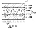
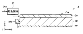
図1は、本技術の第1の実施の形態に係る照明装置1の断面構成を表すものである。この照明装置1は、表示装置のバックライトとして適用可能なものであり、例えば、図1に示したように、導光板10と、導光板10の側面に配置した光源20と、導光板10の背後に配置した光変調素子30および反射板40と、光変調素子30を駆動する駆動回路50とを備えている。
<1. First Embodiment>
FIG. 1 illustrates a cross-sectional configuration of the illumination device 1 according to the first embodiment of the present technology. The illumination device 1 can be applied as a backlight of a display device. For example, as illustrated in FIG. 1, the light guide plate 10, the light source 20 disposed on the side surface of the light guide plate 10, and the light guide plate 10 The light modulation element 30 and the reflection plate 40 disposed behind are provided with a drive circuit 50 that drives the light modulation element 30.

なお、導光板10は、「第1透明基板」または「第2透明基板」の一具体例に相当する。光源20は、「光源」の一具体例に相当する。反射板40は、「反射板」の一具体例に相当する。駆動回路50は、「駆動部」の一具体例に相当する。光源20および光変調素子30からなる光学系が、「照明光学系」の一具体例に相当する。   The light guide plate 10 corresponds to a specific example of “first transparent substrate” or “second transparent substrate”. The light source 20 corresponds to a specific example of “light source”. The reflection plate 40 corresponds to a specific example of “reflection plate”. The drive circuit 50 corresponds to a specific example of a “drive unit”. The optical system including the light source 20 and the light modulation element 30 corresponds to a specific example of “illumination optical system”.

導光板10は、導光板10の側面に配置した光源20からの光を導光板10の上面側(具体的には照明装置1の光出射面1A)に導くものである。導光板10は、例えば、導光板10の上面に配置される被照射物(例えば後述の表示パネル210)に対応した形状になっており、例えば、上面、下面および側面で囲まれた直方体状となっている。なお、以下では、導光板10の側面のうち光源20からの光が入射する側面を光入射面10Aと称するものとする。   The light guide plate 10 guides light from the light source 20 disposed on the side surface of the light guide plate 10 to the upper surface side of the light guide plate 10 (specifically, the light exit surface 1A of the lighting device 1). For example, the light guide plate 10 has a shape corresponding to an object to be irradiated (for example, a display panel 210 described later) disposed on the upper surface of the light guide plate 10. For example, the light guide plate 10 has a rectangular parallelepiped shape surrounded by the upper surface, the lower surface, and the side surfaces. It has become. Hereinafter, the side surface on which light from the light source 20 enters among the side surfaces of the light guide plate 10 is referred to as a light incident surface 10A.

導光板10は、例えば、上面および下面の少なくとも一方の面に、所定のパターン化された形状を有しており、光入射面10Aから入射した光を散乱し、均一化する機能を有している。なお、光変調素子30に印加する電圧を変調することによって輝度の均一化を行う場合には、パターン化されていない平坦な導光板を導光板10として用いることも可能である。導光板10は、例えば、ポリカーボネート樹脂(PC)やアクリル樹脂(ポリメチルメタクリレート(PMMA)などの透明熱可塑性樹脂を主に含んで構成されている。   The light guide plate 10 has, for example, a predetermined patterned shape on at least one of an upper surface and a lower surface, and has a function of scattering and uniformizing light incident from the light incident surface 10A. Yes. In the case where the luminance is uniformed by modulating the voltage applied to the light modulation element 30, a non-patterned flat light guide plate can be used as the light guide plate 10. For example, the light guide plate 10 mainly includes a transparent thermoplastic resin such as polycarbonate resin (PC) or acrylic resin (polymethyl methacrylate (PMMA)).

光源20は、線状光源であり、例えば、熱陰極管(HCFL;Hot Cathode Fluorescent Lamp)、冷陰極管(CCFL;Cold Cathode Fluorescent Lamp)、または複数のLED(Light Emitting Diode)を一列に配置したものなどからなる。光源20が複数のLEDからなる場合には、効率、薄型化、均一性の観点から、全てのLEDがホワイトLEDであることが好ましい。なお、光源20が、例えば、赤色LED、緑色LEDおよび青色LEDを含んで構成されていてもよい。光源20は、導光板10の一の側面にだけ設けられていてもよいし(図1参照)、導光板10の2つの側面、3つの側面または全ての側面に設けられていてもよい。   The light source 20 is a linear light source. For example, a hot cathode fluorescent lamp (HCFL), a cold cathode fluorescent lamp (CCFL), or a plurality of LEDs (Light Emitting Diodes) are arranged in a line. It consists of things. When the light source 20 is composed of a plurality of LEDs, it is preferable that all the LEDs are white LEDs from the viewpoints of efficiency, thickness reduction, and uniformity. The light source 20 may be configured to include, for example, a red LED, a green LED, and a blue LED. The light source 20 may be provided only on one side surface of the light guide plate 10 (see FIG. 1), or may be provided on two side surfaces, three side surfaces, or all side surfaces of the light guide plate 10.

光変調素子30は、本実施の形態において、導光板10の背後(下面)に空気層を介さずに密着しており、例えば接着剤(図示せず)を介して導光板10の背後に接着されている。光変調素子30は、例えば、図2に示したように、透明基板31、下側電極32、配向膜33、光変調層34、配向膜35、上側電極36および透明基板37を反射板40側から順に配置されたものである。なお、下側電極32および上側電極36が「電極」の一具体例に相当する。   In the present embodiment, the light modulation element 30 is in close contact with the back (lower surface) of the light guide plate 10 without an air layer, and is adhered to the back of the light guide plate 10 with an adhesive (not shown), for example. Has been. For example, as illustrated in FIG. 2, the light modulation element 30 includes a transparent substrate 31, a lower electrode 32, an alignment film 33, a light modulation layer 34, an alignment film 35, an upper electrode 36, and a transparent substrate 37 on the reflection plate 40 side. Are arranged in order. The lower electrode 32 and the upper electrode 36 correspond to a specific example of “electrode”.

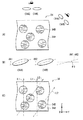
透明基板31,37は、光変調層34を支持するものであり、一般に、可視光に対して透明な基板、例えば、ガラス板や、プラスチックフィルムによって構成されている。上側電極36は、透明基板37のうち透明基板31との対向面上に設けられたものであり、例えば、面内全体に渡って形成された1枚のベタ膜からなる。一方、下側電極32は、透明基板31のうち透明基板37との対向面上に設けられたものであり、例えば、図3に示したように、複数の部分電極32Aによって構成されている。   The transparent substrates 31 and 37 support the light modulation layer 34 and are generally made of a substrate transparent to visible light, such as a glass plate or a plastic film. The upper electrode 36 is provided on the surface of the transparent substrate 37 facing the transparent substrate 31, and is made of, for example, a single solid film formed over the entire surface. On the other hand, the lower electrode 32 is provided on the surface of the transparent substrate 31 facing the transparent substrate 37, and is constituted by a plurality of partial electrodes 32A, for example, as shown in FIG.

複数の部分電極32Aは、例えば、図3に示したように、面内の一の方向(例えば光入射面10Aに平行な方向)に延在する帯状の形状となっている。複数の部分電極32Aのうち特定の複数の部分電極32A(以下、「部分電極32B」と称する。)は、表示装置において三次元表示を行うときに、線状照明光の生成に用いられるものである。複数の部分電極32Bは、表示装置において三次元表示を行うときの画素のピッチP3(図61参照)に対応するピッチP1(画素のピッチP3と同一ピッチまたはそれに近いピッチ)で配列されている。   For example, as shown in FIG. 3, the plurality of partial electrodes 32 </ b> A have a strip shape extending in one direction within the plane (for example, a direction parallel to the light incident surface 10 </ b> A). Among the plurality of partial electrodes 32A, a plurality of specific partial electrodes 32A (hereinafter referred to as “partial electrodes 32B”) are used for generating linear illumination light when performing three-dimensional display in a display device. is there. The plurality of partial electrodes 32B are arranged at a pitch P1 (same or close to the pixel pitch P3) corresponding to the pixel pitch P3 (see FIG. 61) when performing three-dimensional display in the display device.

複数の部分電極32Aのうち部分電極32Bを除く複数の部分電極32A(以下、「部分電極32C」と称する。)は、表示装置において二次元表示を行うときに、部分電極32Aと共に、面状照明光の生成に用いられるものである。つまり、表示装置において二次元表示を行うときには、面状照明光を生成するために、全ての部分電極32Aが用いられる。複数の部分電極32Bおよび複数の部分電極32Cは、光入射面10Aと直交する方向において規則的に配列されている。例えば、図2、図3に示したように、1つの部分電極32Bおよび2つの部分電極32Cを一組として、複数組の部分電極群が光入射面10Aと直交する方向に配列されている。部分電極32Bの幅は、例えば、表示装置の画素の幅よりも狭くなっている。   Among the plurality of partial electrodes 32A, a plurality of partial electrodes 32A (hereinafter referred to as “partial electrodes 32C”) excluding the partial electrode 32B, together with the partial electrodes 32A, are used for planar illumination when performing two-dimensional display on the display device. It is used for light generation. That is, when performing two-dimensional display in the display device, all the partial electrodes 32A are used to generate planar illumination light. The plurality of partial electrodes 32B and the plurality of partial electrodes 32C are regularly arranged in a direction orthogonal to the light incident surface 10A. For example, as shown in FIGS. 2 and 3, one partial electrode 32B and two partial electrodes 32C are used as a set, and a plurality of sets of partial electrodes are arranged in a direction orthogonal to the light incident surface 10A. For example, the width of the partial electrode 32B is narrower than the width of the pixel of the display device.

各部分電極32Aは、例えば、図4に示したように、ブロック形状となっており、かつ複数の部分電極32Aが2次元配置されていてもよい。この場合には、複数の部分電極32Aを1つの線状電極32Dとみなしたときに、各線状電極32Dが上記の部分電極32B,32Cとして用いられてもよい。例えば、複数の線状電極32Dのうち特定の複数の線状電極32Dが、部分電極32Bとして用いられる。複数の線状電極32Dのうち部分電極32Bとして用いられるものを除く複数の線状電極32Dが、部分電極32Cとして用いられる。   For example, as shown in FIG. 4, each partial electrode 32A has a block shape, and a plurality of partial electrodes 32A may be two-dimensionally arranged. In this case, when the plurality of partial electrodes 32A are regarded as one linear electrode 32D, each linear electrode 32D may be used as the partial electrodes 32B and 32C. For example, a specific plurality of linear electrodes 32D among the plurality of linear electrodes 32D are used as the partial electrodes 32B. A plurality of linear electrodes 32D excluding those used as the partial electrode 32B among the plurality of linear electrodes 32D are used as the partial electrode 32C.

なお、各部分電極32Aがブロック形状となっており、かつ複数の部分電極32Aが2次元配置されている場合に、表示装置において三次元表示を行うときに、個々の部分電極32Aが点状照明光の生成に用いられてもよい。また、各部分電極32Aがブロック形状となっており、かつ複数の部分電極32Aが2次元配置されている場合に、表示装置において2視点から互いに異なる二次元映像を視認可能な二次元表示を行うときにも、個々の部分電極32Aが点状照明光の生成に用いられてもよい。   When each partial electrode 32A has a block shape and a plurality of partial electrodes 32A are arranged two-dimensionally, when performing three-dimensional display on the display device, each partial electrode 32A has a point illumination. It may be used for light generation. In addition, when each partial electrode 32A has a block shape and a plurality of partial electrodes 32A are two-dimensionally arranged, the display device performs two-dimensional display in which different two-dimensional images can be viewed from two viewpoints. Sometimes, the individual partial electrodes 32A may be used to generate the point illumination light.

また、例えば、図5、図6に示したように、互いに隣接する部分電極32B同士の間に、部分電極32Bの幅よりも広い幅の部分電極32Cが設けられていてもよい。このとき、さらに、例えば、図7に示したように、各部分電極32Bが複数の部分電極32Aで構成されると共に、各部分電極32Cが複数の部分電極32Aで構成されていてもよい。   For example, as shown in FIGS. 5 and 6, a partial electrode 32C having a width wider than the width of the partial electrode 32B may be provided between the adjacent partial electrodes 32B. At this time, for example, as shown in FIG. 7, each partial electrode 32B may be composed of a plurality of partial electrodes 32A, and each partial electrode 32C may be composed of a plurality of partial electrodes 32A.

また、例えば、図8に示したように、各部分電極32Aが、光入射面10Aと直角以外の角度で斜めに交差する方向に延在していてもよい。また、各部分電極32Aがブロック形状となっており、かつ複数の部分電極32Aが2次元配置されている場合に、例えば、図9に示したように、各線状電極32Dが、光入射面10Aと直角以外の角度で斜めに交差する方向に延在していてもよい。なお、各部分電極32Aが光入射面10Aの法線と斜めに交差する方向に延在している場合に、各部分電極32Aの延在方向が、後述の表示パネル210の画素の配列方向と交差する方向に延在していることが好ましい。このようにした場合には、三次元表示時に、光入射面10Aの法線と平行な方向の解像度と、光入射面10Aと平行な方向の解像度との差を小さくすることができる。   Further, for example, as shown in FIG. 8, each partial electrode 32A may extend in a direction that obliquely intersects with the light incident surface 10A at an angle other than a right angle. When each partial electrode 32A has a block shape and a plurality of partial electrodes 32A are two-dimensionally arranged, for example, as shown in FIG. 9, each linear electrode 32D has a light incident surface 10A. And may extend in a direction obliquely intersecting at an angle other than a right angle. When each partial electrode 32A extends in a direction that obliquely intersects the normal line of the light incident surface 10A, the extending direction of each partial electrode 32A corresponds to the pixel arrangement direction of the display panel 210 described later. It is preferable to extend in the intersecting direction. In this case, at the time of three-dimensional display, the difference between the resolution in the direction parallel to the normal line of the light incident surface 10A and the resolution in the direction parallel to the light incident surface 10A can be reduced.

下側電極32および上側電極36はともに、透明導電膜によって構成されている。この透明導電膜は、例えば、以下の式で示されるような特性を有していることが好ましい(図10(A)参照)。この透明導電膜は、例えば、ITOを含む膜(以下、「ITO膜」と称する。)によって構成されている。なお、下側電極32および上側電極36は、酸化インジウム亜鉛(IZO;Indium Zinc Oxide)、メタルナノワイヤ、カーボンナノチューブ、グラフェンなどによって構成されていてもよい。   Both the lower electrode 32 and the upper electrode 36 are made of a transparent conductive film. The transparent conductive film preferably has, for example, characteristics shown by the following formula (see FIG. 10A). This transparent conductive film is composed of, for example, a film containing ITO (hereinafter referred to as “ITO film”). The lower electrode 32 and the upper electrode 36 may be made of indium zinc oxide (IZO), metal nanowires, carbon nanotubes, graphene, or the like.

|A1−A2|≦2.00
A1:450nm〜650nmにおける最大光吸収率(%)
A2:450nm〜650nmにおける最小光吸収率(%)
| A1-A2 | ≦ 2.00
A1: Maximum light absorption rate (%) at 450 nm to 650 nm
A2: Minimum light absorption rate (%) at 450 nm to 650 nm

照明光としては、可視光が使用されるので、380〜780nmの範囲で、透明導電膜の光吸収の差が少ないことが好ましい。380〜780nmの範囲で光吸収率の最大値と最小値の差が、10.00以下であることが好ましく、7.00以下であることがより好ましい。特に、透明導電膜がバックライトなどに適用される場合は、使用する光源の波長領域の範囲内で光吸収率の最大値と最小値の差が2.00以下であることが好ましく、1.00以下であることがより好ましい。一般的なLEDを光源として光源などを用いた場合、450〜650nm範囲で、光吸収率の最大値と最小値の差が、2.00以下であることが好ましく、1.00以下であることがより好ましい。なお、吸収率の測定は日本分光製V−550を用い、基板法線方向から5°入射にて反射率、透過率を測定し、100%から反射率、透過率の値を引いた値を吸収率とした。   Since visible light is used as the illumination light, it is preferable that the difference in light absorption of the transparent conductive film is small in the range of 380 to 780 nm. In the range of 380 to 780 nm, the difference between the maximum value and the minimum value of the light absorption rate is preferably 10.00 or less, and more preferably 7.00 or less. In particular, when the transparent conductive film is applied to a backlight or the like, the difference between the maximum value and the minimum value of the light absorptance is preferably 2.00 or less within the wavelength range of the light source used. More preferably, it is 00 or less. When a light source or the like is used with a general LED as a light source, the difference between the maximum value and the minimum value of the light absorption rate is preferably 2.00 or less and is 1.00 or less in the range of 450 to 650 nm. Is more preferable. The absorptance was measured using JASCO V-550, the reflectance and transmittance were measured at 5 ° incidence from the substrate normal direction, and the value obtained by subtracting the reflectance and transmittance values from 100% was obtained. Absorption rate.

このように、透明導電膜が上記の式に示した特性となっている場合には、光源20から出射された光が導光板10内を伝播していく過程で光変調素子30内の透明導電膜を繰り返し通過したときに、透明導電膜における、吸収の波長依存性が抑制される。透明導電膜が、一般的なITO膜からなる場合には、例えば、図10(B),(C)の破線および図11(A)の矢印に示したように、光源20からの距離が遠くなるにつれて、長波長側の成分が増大していく。一方、透明導電膜が、上記の式に示した特性を有する、膜質改善されたITO膜からなる場合には、例えば、図10(B),(C)の実線および図11(B)に示したように、長波長側の成分が光源20からの距離に応じて変化する割合が低減している。なお、図10(B),(C)の縦軸のΔu’v’は、その値が大きくなるほど、長波長側の成分が大きくなることに対応する指標である。   As described above, when the transparent conductive film has the characteristics shown in the above equation, the transparent conductive film in the light modulation element 30 is transmitted in the process in which the light emitted from the light source 20 propagates in the light guide plate 10. When repeatedly passing through the film, the wavelength dependence of absorption in the transparent conductive film is suppressed. When the transparent conductive film is made of a general ITO film, for example, the distance from the light source 20 is long as shown by the broken lines in FIGS. 10B and 10C and the arrow in FIG. As it becomes, the component on the long wavelength side increases. On the other hand, when the transparent conductive film is made of an ITO film having the characteristics shown in the above formula and improved in film quality, for example, the solid lines shown in FIGS. 10 (B) and (C) and FIG. 11 (B). As described above, the rate at which the component on the long wavelength side changes according to the distance from the light source 20 is reduced. Note that Δu′v ′ on the vertical axis in FIGS. 10B and 10C is an index corresponding to an increase in the component on the long wavelength side as the value increases.

また、例えば、下側電極32および上側電極36がITO膜によって構成されているとき、導光している光路中のどこか(例えば、導光板10および光変調素子30の少なくとも一方)に、例えば、長波長側の光を短波長側の光よりもより多く吸収する染料・顔料が含まれていることが好ましい。上記の染料・顔料として、公知の材料を使用することができる。特に、光変調層34の形成に紫外線照射によるプロセスを含む場合には、例えば、光変調素子30を形成した後に、染料・顔料を含む導光板10と光変調素子30とを互いに貼り合わせたり、染料・顔料が紫外線によってダメージを受けないように、染料・顔料を含む部分を紫外線吸収層で紫外線から保護することが好ましい。このように、導光している光路中のどこかに上記の染料・顔料を添加することにより、光源20から出射された光が導光板10内を伝播していく過程で光変調素子30を繰り返し通過したときに、ITO膜を含む光変調素子30の吸収の波長依存性が抑制される。   In addition, for example, when the lower electrode 32 and the upper electrode 36 are made of an ITO film, somewhere in the light guide path (for example, at least one of the light guide plate 10 and the light modulation element 30), for example, It is preferable that a dye / pigment that absorbs light on the long wavelength side more than light on the short wavelength side is contained. Known materials can be used as the above-mentioned dyes and pigments. In particular, in the case where the formation of the light modulation layer 34 includes a process by ultraviolet irradiation, for example, after the light modulation element 30 is formed, the light guide plate 10 containing the dye / pigment and the light modulation element 30 are bonded to each other, In order to prevent the dye / pigment from being damaged by the ultraviolet rays, it is preferable to protect the portion containing the dye / pigment from the ultraviolet rays by the ultraviolet absorbing layer. In this way, by adding the above dye / pigment somewhere in the light path being guided, the light modulation element 30 is changed in the process in which the light emitted from the light source 20 propagates through the light guide plate 10. When it passes repeatedly, the wavelength dependence of the absorption of the light modulation element 30 including the ITO film is suppressed.

下側電極32および上側電極36を光変調素子30の法線方向から見たときに、光変調素子30のうち下側電極32および上側電極36が互いに対向している箇所に対応する部分が光変調セル30−1を構成している(図2、図5参照)。   When the lower electrode 32 and the upper electrode 36 are viewed from the normal direction of the light modulation element 30, a portion of the light modulation element 30 corresponding to a portion where the lower electrode 32 and the upper electrode 36 face each other is light. A modulation cell 30-1 is configured (see FIGS. 2 and 5).

光変調セル30−1は、光変調素子30のうち部分電極32Aおよび上側電極36が互いに対向している箇所に対応する部分に相当する。複数の光変調セル30−1のうち部分電極32Bを含むセル30a(図2〜図9参照)が、表示装置において三次元表示を行うときに、線状照明光の生成に用いられる。複数の光変調セル30−1のうち部分電極32Cを含むセル30b(図2〜図9参照)が、表示装置において二次元表示を行うときに、複数のセル30aと共に、面状照明光の生成に用いられる。つまり、表示装置において二次元表示を行うときには、面状照明光を生成するために、全ての光変調セル30−1が用いられる。   The light modulation cell 30-1 corresponds to a portion of the light modulation element 30 corresponding to a portion where the partial electrode 32A and the upper electrode 36 face each other. A cell 30a (see FIGS. 2 to 9) including the partial electrode 32B among the plurality of light modulation cells 30-1 is used to generate linear illumination light when performing three-dimensional display in the display device. When the cell 30b (see FIGS. 2 to 9) including the partial electrode 32C among the plurality of light modulation cells 30-1 performs two-dimensional display in the display device, the planar illumination light is generated together with the plurality of cells 30a. Used for. That is, when two-dimensional display is performed on the display device, all the light modulation cells 30-1 are used to generate planar illumination light.

各光変調セル30−1は、部分電極32Aおよび上側電極36に所定の電圧を印加することにより別個独立に駆動することの可能なものであり、部分電極32Aおよび上側電極36に印加される電圧値の大きさに応じて、光源20からの光に対して透明性を示したり、散乱性を示したりする。なお、透明性、散乱性については、光変調層34を説明する際に詳細に説明する。   Each light modulation cell 30-1 can be driven independently by applying a predetermined voltage to the partial electrode 32A and the upper electrode 36, and the voltage applied to the partial electrode 32A and the upper electrode 36. Depending on the magnitude of the value, the light from the light source 20 is transparent or scattering. The transparency and scattering properties will be described in detail when the light modulation layer 34 is described.

配向膜33,35は、例えば、光変調層34に用いられる液晶やモノマーを配向させるものである。配向膜の種類としては、例えば、垂直配向膜および水平配向膜があるが、本実施の形態では、配向膜33,35には水平配向膜が用いられる。水平配向膜としては、例えば、ポリイミド、ポリアミドイミド、ポリビニルアルコールなどをラビング処理することにより形成された配向膜、転写やエッチングなどにより溝形状が付与された配向膜が挙げられる。また、水平配向膜としては、例えば、酸化ケイ素などの無機材料を斜方蒸着することにより形成された配向膜、イオンビーム照射により形成されたダイヤモンドライクカーボン配向膜、電極パターンスリットの形成された配向膜が挙げられる。透明基板31,37としてプラスチックフィルムを用いる場合には、製造工程において、透明基板31,37の表面に配向膜33,35を塗布した後の焼成温度ができるだけ低いことが好ましいことから、配向膜33,35として、100℃以下の温度で形成可能なポリアミドイミドを用いることが好ましい。   For example, the alignment films 33 and 35 align liquid crystals and monomers used in the light modulation layer 34. Examples of the alignment film include a vertical alignment film and a horizontal alignment film. In this embodiment, horizontal alignment films are used as the alignment films 33 and 35. Examples of the horizontal alignment film include an alignment film formed by rubbing polyimide, polyamideimide, polyvinyl alcohol, and the like, and an alignment film provided with a groove shape by transfer or etching. In addition, as the horizontal alignment film, for example, an alignment film formed by oblique deposition of an inorganic material such as silicon oxide, a diamond-like carbon alignment film formed by ion beam irradiation, an alignment formed with an electrode pattern slit A membrane is mentioned. When a plastic film is used as the transparent substrates 31 and 37, it is preferable that the firing temperature after applying the alignment films 33 and 35 on the surfaces of the transparent substrates 31 and 37 in the manufacturing process is as low as possible. , 35 is preferably a polyamideimide that can be formed at a temperature of 100 ° C. or lower.

また、垂直、水平いずれの配向膜においても、液晶とモノマーを配向させる機能があれば十分であり、通常の液晶ディスプレイに要求される電圧の繰り返し印加による信頼性などは必要ない。デバイス作成後の電圧印加による信頼性は、モノマーを重合したものと液晶との界面で決まるためである。また、配向膜を用いなくても、例えば、下側電極32および上側電極36間に電場や磁場を印加することによっても、光変調層34に用いられる液晶やモノマーを配向させることが可能である。つまり、下側電極32および上側電極36間に電場や磁場を印加しながら、紫外線照射して電圧印加状態での液晶やモノマーの配向状態を固定させることができる。配向膜の形成に電圧を用いる場合には、配向用と駆動用とで別々の電極を形成するか、液晶材料に周波数によって誘電率異方性の符号が反転する二周波液晶などを用いることができる。また、配向膜の形成に磁場を用いる場合、配向膜として磁化率異方性の大きい材料を用いることが好ましく、例えば、ベンゼン環の多い材料を用いることが好ましい。   Further, both the vertical and horizontal alignment films need only have a function of aligning the liquid crystal and the monomer, and do not require reliability due to repeated application of voltage required for a normal liquid crystal display. This is because the reliability due to the voltage application after device fabrication is determined by the interface between the polymerized monomer and the liquid crystal. Further, without using an alignment film, for example, by applying an electric field or a magnetic field between the lower electrode 32 and the upper electrode 36, it is possible to align the liquid crystal or monomer used for the light modulation layer 34. . That is, while applying an electric field or a magnetic field between the lower electrode 32 and the upper electrode 36, it is possible to fix the alignment state of the liquid crystal or the monomer in the voltage application state by irradiating with ultraviolet rays. When a voltage is used to form the alignment film, separate electrodes for alignment and driving may be formed, or a two-frequency liquid crystal in which the sign of dielectric anisotropy is inverted depending on the frequency may be used for the liquid crystal material. it can. Further, when a magnetic field is used for forming the alignment film, it is preferable to use a material having a large magnetic anisotropy as the alignment film, for example, a material having many benzene rings.

光変調層34は、電場の大きさに応じて、光源20からの光に対して散乱性もしくは透明性を示すものである。光変調層34は、電場が相対的に小さいときに、光源20からの光に対して透明性を示し、電場が相対的に大きいときに、光源20からの光に対して散乱性を示すものである。光変調層34は、例えば、図2に示したように、バルク34Aと、バルク34A内に分散された微粒子状の複数の微粒子34Bとを含んだ複合層となっている。バルク34Aおよび微粒子34Bは光学異方性を有している。   The light modulation layer 34 exhibits scattering or transparency with respect to the light from the light source 20 depending on the magnitude of the electric field. The light modulation layer 34 exhibits transparency with respect to light from the light source 20 when the electric field is relatively small, and exhibits scattering with respect to light from the light source 20 when the electric field is relatively large. It is. For example, as shown in FIG. 2, the light modulation layer 34 is a composite layer including a bulk 34A and a plurality of fine particles 34B dispersed in the bulk 34A. The bulk 34A and the fine particles 34B have optical anisotropy.

図12(A)は、下側電極32および上側電極36間に電圧が印加されていない時の、微粒子34B内の配向状態の一例を模式的に表したものである。なお、図12(A)において、バルク34A内の配向状態についての記載を省略した。図12(B)は、下側電極32および上側電極36間に電圧が印加されていない時の、バルク34Aおよび微粒子34Bの屈折率異方性を示す屈折率楕円体の一例を表したものである。この屈折率楕円体は、様々な方向から入射した直線偏光の屈折率をテンソル楕円体で表したものであり、光が入射する方向からの楕円体の断面を見ることによって、幾何的に屈折率を知ることができるものである。図12(C)は、下側電極32および上側電極36間に電圧が印加されていない時の、正面方向に向かう光L1と、斜め方向に向かう光L2とが光変調層34を透過する様子の一例を模式的に表したものである。   FIG. 12A schematically shows an example of the orientation state in the fine particles 34B when no voltage is applied between the lower electrode 32 and the upper electrode 36. In FIG. 12A, description of the orientation state in the bulk 34A is omitted. FIG. 12B shows an example of a refractive index ellipsoid showing the refractive index anisotropy of the bulk 34A and the fine particles 34B when no voltage is applied between the lower electrode 32 and the upper electrode 36. is there. This refractive index ellipsoid is a tensor ellipsoid representing the refractive index of linearly polarized light incident from various directions. By looking at the cross section of the ellipsoid from the light incident direction, the refractive index is geometrically It is something that can know. FIG. 12C shows a state in which light L1 traveling in the front direction and light L2 traveling in the oblique direction pass through the light modulation layer 34 when no voltage is applied between the lower electrode 32 and the upper electrode 36. Is an example schematically.

図13(A)は、下側電極32および上側電極36間に電圧が印加されている時の、微粒子34B内の配向状態の一例を模式的に表したものである。なお、図13(A)において、バルク34A内の配向状態についての記載を省略した。図13(B)は、下側電極32および上側電極36間に電圧が印加されている時の、バルク34Aおよび微粒子34Bの屈折率異方性を示す屈折率楕円体の一例を表したものである。図13(C)は、下側電極32および上側電極36間に電圧が印加されている時の、正面方向に向かう光L1と、斜め方向に向かう光L2とが光変調層34において散乱される様子の一例を模式的に表したものである。   FIG. 13A schematically shows an example of the orientation state in the fine particles 34 </ b> B when a voltage is applied between the lower electrode 32 and the upper electrode 36. In FIG. 13A, description of the orientation state in the bulk 34A is omitted. FIG. 13B shows an example of a refractive index ellipsoid showing refractive index anisotropy of the bulk 34A and the fine particles 34B when a voltage is applied between the lower electrode 32 and the upper electrode 36. FIG. is there. FIG. 13C shows that the light L1 traveling in the front direction and the light L2 traveling in the oblique direction when the voltage is applied between the lower electrode 32 and the upper electrode 36 are scattered in the light modulation layer 34. An example of the state is schematically shown.

バルク34Aおよび微粒子34Bは、例えば、図12(A),(B)に示したように、下側電極32および上側電極36間に電圧が印加されていない時に、バルク34Aの光軸AX1および微粒子34Bの光軸AX2の向きが互いに一致する(平行となる)構成となっている。なお、光軸AX1,AX2とは、偏光方向によらず屈折率が一つの値になるような光線の進行方向と平行な線を指している。また、光軸AX1および光軸AX2の向きは常に互いに一致している必要はなく、光軸AX1の向きと光軸AX2の向きとが、例えば製造誤差などによって多少ずれていてもよい。   For example, as shown in FIGS. 12A and 12B, the bulk 34A and the fine particles 34B are obtained when the voltage is not applied between the lower electrode 32 and the upper electrode 36, and the optical axis AX1 and fine particles of the bulk 34A. The direction of the optical axis AX2 of 34B coincides with (becomes parallel to) each other. The optical axes AX1 and AX2 indicate lines parallel to the traveling direction of the light beam so that the refractive index becomes one value regardless of the polarization direction. Further, the directions of the optical axis AX1 and the optical axis AX2 do not always have to coincide with each other, and the direction of the optical axis AX1 and the direction of the optical axis AX2 may be slightly shifted due to, for example, a manufacturing error.

また、微粒子34Bは、例えば、下側電極32および上側電極36間に電圧が印加されていない時に、光軸AX2が導光板10の光入射面10Aと平行となる構成となっている。微粒子34Bは、さらに、例えば、下側電極32および上側電極36間に電圧が印加されていない時に、光軸AX2が透明基板31,37の表面と僅かな角度θ1で交差する構成となっている(図12(B)参照)。なお、角度θ1については、微粒子34Bを構成する材料を説明する際に詳述する。   The fine particles 34B have a configuration in which, for example, the optical axis AX2 is parallel to the light incident surface 10A of the light guide plate 10 when no voltage is applied between the lower electrode 32 and the upper electrode 36. The fine particles 34B further have a configuration in which, for example, the optical axis AX2 intersects the surfaces of the transparent substrates 31 and 37 at a slight angle θ1 when no voltage is applied between the lower electrode 32 and the upper electrode 36. (See FIG. 12B). The angle θ1 will be described in detail when describing the material constituting the fine particles 34B.

一方、バルク34Aは、例えば、下側電極32および上側電極36間への電圧印加の有無に拘らず、バルク34Aの光軸AX1が一定となる構成となっている。具体的には、バルク34Aは、例えば、図12(A),(B),図13(A),(B)に示したように、バルク34Aの光軸AX1が導光板10の光入射面10Aと平行となると共に透明基板31,37の表面と所定の角度θ1で交差する構成となっている。つまり、バルク34Aの光軸AX1は、下側電極32および上側電極36間に電圧が印加されていない時に、微粒子34Bの光軸AX2と平行となっている。   On the other hand, the bulk 34A has a configuration in which, for example, the optical axis AX1 of the bulk 34A is constant regardless of whether or not a voltage is applied between the lower electrode 32 and the upper electrode 36. Specifically, the bulk 34 </ b> A has an optical axis AX <b> 1 of the bulk 34 </ b> A whose light incident surface of the light guide plate 10, as shown in FIGS. 12A, 12 </ b> B, 13 </ b> A, 13 </ b> B, for example. 10A and parallel to the surface of the transparent substrates 31 and 37 at a predetermined angle θ1. That is, the optical axis AX1 of the bulk 34A is parallel to the optical axis AX2 of the fine particles 34B when no voltage is applied between the lower electrode 32 and the upper electrode 36.

なお、光軸AX2が常に、光入射面10Aと平行となると共に透明基板31,37の表面と角度θ1で交差している必要はなく、例えば製造誤差などによって透明基板31,37の表面と、角度θ1とは若干異なる角度で交差していてもよい。また、光軸AX1,AX2が常に光入射面10Aと平行となっている必要はなく、例えば製造誤差などによって光入射面10Aと、小さな角度で交差していてもよい。   The optical axis AX2 is always parallel to the light incident surface 10A and does not need to intersect the surfaces of the transparent substrates 31 and 37 at an angle θ1, for example, due to manufacturing errors, It may intersect at an angle slightly different from the angle θ1. The optical axes AX1 and AX2 do not always have to be parallel to the light incident surface 10A, and may intersect the light incident surface 10A at a small angle due to, for example, manufacturing errors.

ここで、バルク34Aおよび微粒子34Bの常光屈折率が互いに等しく、かつバルク34Aおよび微粒子34Bの異常光屈折率が互いに等しいことが好ましい。この場合に、例えば、下側電極32および上側電極36間に電圧が印加されていない時には、図12(A)に示したように、正面方向および斜め方向を含むあらゆる方向において屈折率差がほとんどなく、高い透明性が得られる。これにより、例えば、図12(C)に示したように、正面方向に向かう光L1および斜め方向に向かう光L2は、光変調層34内で散乱されることなく、光変調層34を透過する。その結果、例えば、図14(A),(B)に示したように、光源20からの光L(斜め方向からの光)は、光変調層34のうち透明な領域(透過領域30A)の界面(透明基板31の下面および導光板10の上面)において全反射され、透過領域30Aの輝度(黒表示の輝度)が、全面を均一に発光させた場合(図14(B)中の一点鎖線)と比べて下がる。なお、図14(B)の正面輝度のプロファイルは、導光板10上に拡散シート(図示せず)を設置し、その拡散シートを介して測定することにより得られたものである。   Here, it is preferable that the ordinary light refractive indexes of the bulk 34A and the fine particles 34B are equal to each other, and the extraordinary refractive indexes of the bulk 34A and the fine particles 34B are equal to each other. In this case, for example, when no voltage is applied between the lower electrode 32 and the upper electrode 36, as shown in FIG. 12A, there is almost no difference in refractive index in all directions including the front direction and the oblique direction. And high transparency is obtained. Thereby, for example, as shown in FIG. 12C, the light L1 traveling in the front direction and the light L2 traveling in the oblique direction pass through the light modulation layer 34 without being scattered in the light modulation layer 34. . As a result, for example, as shown in FIGS. 14A and 14B, the light L from the light source 20 (light from an oblique direction) is transmitted from the transparent region (transmission region 30A) of the light modulation layer 34. When the light is totally reflected at the interface (the lower surface of the transparent substrate 31 and the upper surface of the light guide plate 10), and the luminance of the transmissive region 30A (black display luminance) is uniformly emitted over the entire surface (the chain line in FIG. 14B) ) And lower. 14B is obtained by installing a diffusion sheet (not shown) on the light guide plate 10 and measuring through the diffusion sheet.

なお、透過領域30Aの界面の1つである導光板10の上面(図14中では光出射面1A)は、当該照明装置1が表示装置のバックライトとして用いられたときに、導光板10の上面が、導光板10の上面の屈折率よりも低い屈折率の材料と接していることが好ましい。そのような低屈折率材料は、典型的には空気である。なお、当該照明装置1が表示装置のバックライトとして用いられたときに、導光板10の上面が表示装置内の他の光学部材(例えば表示パネル)と接着されている場合には、導光板10の上面に接する低屈折率材料は、粘着剤もしくは接着剤であってもよい。   Note that the upper surface of the light guide plate 10 (the light exit surface 1A in FIG. 14), which is one of the interfaces of the transmissive region 30A, is the surface of the light guide plate 10 when the illumination device 1 is used as a backlight of a display device. It is preferable that the upper surface is in contact with a material having a refractive index lower than that of the upper surface of the light guide plate 10. Such a low refractive index material is typically air. When the lighting device 1 is used as a backlight of a display device, the light guide plate 10 is used when the upper surface of the light guide plate 10 is bonded to another optical member (for example, a display panel) in the display device. The low refractive index material in contact with the upper surface may be an adhesive or an adhesive.

バルク34Aおよび微粒子34Bは、例えば、下側電極32および上側電極36間に電圧が印加されている時には、図13(A),(B)に示したように、光軸AX1および光軸AX2の向きが互いに異なる(交差またはほぼ直交する)構成となっている。また、微粒子34Bは、例えば、下側電極32および上側電極36間に電圧が印加されている時に、微粒子34Bの光軸AX2が導光板10の光入射面10Aと平行となると共に透明基板31,37の表面と角度θ1よりも大きな角度θ2(例えば90°)で交差する構成となっている。なお、角度θ2については、微粒子34Bを構成する材料を説明する際に詳述する。   For example, when a voltage is applied between the lower electrode 32 and the upper electrode 36, the bulk 34A and the fine particles 34B have an optical axis AX1 and an optical axis AX2 as shown in FIGS. The directions are different from each other (intersecting or almost orthogonal). For example, when a voltage is applied between the lower electrode 32 and the upper electrode 36, the fine particle 34B has the optical axis AX2 of the fine particle 34B parallel to the light incident surface 10A of the light guide plate 10 and the transparent substrate 31, It intersects with the surface of 37 at an angle θ2 (for example, 90 °) larger than the angle θ1. The angle θ2 will be described in detail when the material constituting the fine particles 34B is described.

したがって、下側電極32および上側電極36間に電圧が印加されている時には、光変調層34において、正面方向および斜め方向を含むあらゆる方向において屈折率差が大きくなり、高い散乱性が得られる。これにより、例えば、図13(C)に示したように、正面方向に向かう光L1および斜め方向に向かう光L2は、光変調層34内で散乱される。その結果、例えば、図14(A)に示したように、光源20からの光L(斜め方向からの光)は、散乱領域30Bの界面(透明基板31または導光板10と空気との界面)を透過すると共に、反射板40側に透過した光は反射板40で反射され、光変調素子30を透過する。従って、散乱領域30Bの輝度は、全面を均一に発光させた場合(図14(B)中の一点鎖線)と比べて極めて高くなり、しかも、透過領域30Aの輝度が低下した分だけ、部分的な白表示の輝度(輝度突き上げ)が大きくなる。なお、散乱領域30Bが本技術の「第1領域」の一具体例に相当する。   Therefore, when a voltage is applied between the lower electrode 32 and the upper electrode 36, the refractive index difference increases in all directions including the front direction and the oblique direction in the light modulation layer 34, and a high scattering property is obtained. Thereby, for example, as illustrated in FIG. 13C, the light L <b> 1 traveling in the front direction and the light L <b> 2 traveling in the oblique direction are scattered in the light modulation layer 34. As a result, for example, as shown in FIG. 14A, the light L from the light source 20 (light from an oblique direction) is an interface of the scattering region 30B (an interface between the transparent substrate 31 or the light guide plate 10 and air). And the light transmitted to the reflecting plate 40 side is reflected by the reflecting plate 40 and passes through the light modulation element 30. Therefore, the brightness of the scattering region 30B is extremely higher than that when the entire surface is made to emit light uniformly (the alternate long and short dash line in FIG. 14B), and the brightness of the transmission region 30A is partially reduced. The brightness of bright white display (increased brightness) increases. The scattering region 30B corresponds to a specific example of “first region” of the present technology.

なお、バルク34Aおよび微粒子34Bの常光屈折率は、例えば製造誤差などによって多少ずれていてもよく、例えば、0.1以下であることが好ましく、0.05以下であることがより好ましい。また、バルク34Aおよび微粒子34Bの異常光屈折率についても、例えば製造誤差などによって多少ずれていてもよく、例えば、0.1以下であることが好ましく、0.05以下であることがより好ましい。   Note that the ordinary refractive indexes of the bulk 34A and the fine particles 34B may be slightly deviated due to, for example, manufacturing errors, and are preferably 0.1 or less, and more preferably 0.05 or less. Further, the extraordinary light refractive indexes of the bulk 34A and the fine particles 34B may be slightly deviated due to, for example, manufacturing errors, and are preferably 0.1 or less, and more preferably 0.05 or less.

また、バルク34Aの屈折率差(ΔnP=異常光屈折率neP−常光屈折率noP)や、微粒子34Bの屈折率差(ΔnL=異常光屈折率neL−常光屈折率noL)は、できるだけ大きいことが好ましく、0.05以上であることが好ましく、0.1以上であることがより好ましく、0.15以上であることがさらに好ましい。バルク34Aおよび微粒子34Bの屈折率差が大きい場合には、光変調層34の散乱能が高くなり、導光条件を容易に破壊することができ、導光板10からの光を取り出しやすいからである。 Further, the refractive index difference of the bulk 34A (Δn P = extraordinary light refractive index ne P −normal light refractive index no P ) and the refractive index difference of the fine particles 34B (Δn L = abnormal light refractive index ne L −normal light refractive index no L ). Is preferably as large as possible, preferably 0.05 or more, more preferably 0.1 or more, and still more preferably 0.15 or more. This is because, when the difference in refractive index between the bulk 34A and the fine particles 34B is large, the light modulation layer 34 has a high scattering ability, the light guide conditions can be easily broken, and the light from the light guide plate 10 can be easily taken out. .

また、バルク34Aおよび微粒子34Bは、電場に対する応答速度が互いに異なっている。バルク34Aは、例えば、微粒子34Bの応答速度よりも遅い応答速度を有する筋状構造(図15(A),(B)参照)、多孔質構造、または棒状構造となっている。なお、図15(A),(B)は、光変調素子30に対して電場を印加したときの偏光顕微鏡写真であり、図15(A),(B)中で筋状に明るい箇所が上述した筋状構造に相当している。図15(A)には、液晶とモノマーの重量比を95:5としたときのバルク34Aの筋状構造の様子が示されており、図15(B)には、液晶とモノマーの重量比を90:10としたときのバルク34Aの筋状構造の様子が示されている。バルク34Aは、例えば、低分子モノマーを重合化することにより得られた高分子材料によって形成されている。バルク34Aは、例えば、微粒子34Bの配向方向または配向膜33,35の配向方向に沿って配向した、配向性および重合性を有する材料(例えばモノマー)を熱および光の少なくとも一方によって重合させることにより形成されている。   Further, the bulk 34A and the fine particles 34B have different response speeds with respect to the electric field. The bulk 34A has, for example, a streak structure (see FIGS. 15A and 15B) having a response speed slower than the response speed of the fine particles 34B, a porous structure, or a rod-like structure. 15A and 15B are polarization micrographs when an electric field is applied to the light modulation element 30, and the streaky bright portions in FIGS. 15A and 15B are described above. This corresponds to the streaky structure. FIG. 15A shows the streaky structure of the bulk 34A when the weight ratio of liquid crystal to monomer is 95: 5, and FIG. 15B shows the weight ratio of liquid crystal to monomer. The state of the streaky structure of the bulk 34A when the ratio is 90:10 is shown. The bulk 34A is formed of, for example, a polymer material obtained by polymerizing a low molecular weight monomer. For example, the bulk 34A is obtained by polymerizing a material having alignment properties and polymerizability (for example, a monomer) aligned along the alignment direction of the fine particles 34B or the alignment direction of the alignment films 33 and 35 with at least one of heat and light. Is formed.

バルク34Aの筋状構造、多孔質構造もしくは棒状構造は、例えば、導光板10の光入射面10Aと平行となると共に透明基板31,37の表面と僅かな角度θ1で交差する方向に長軸を有している。バルク34Aが筋状構造となっている場合に、短軸方向の平均的な筋状組織サイズは、導光光の散乱性を高くするという観点からは、0.1μm以上10μm以下となっていることが好ましく、0.2μm以上2.0μm以下の範囲であることがより好ましい。短軸方向の平均的な筋状組織サイズが0.1μm以上10μm以下となっている場合には、光変調素子30内での散乱能が、380〜780nmの可視領域において略等しくなる。そのため、面内で、ある特定の波長成分の光のみが増加したり、減少したりすることがないので、可視領域でのバランスを面内で取ることができる。短軸方向の平均的な筋状組織サイズが0.1μm未満である場合や、10μmを超える場合には、波長に関係なく、光変調素子30の散乱能が低く、光変調素子30が光変調素子として機能しにくい。   The streaky structure, the porous structure, or the rod-shaped structure of the bulk 34A is, for example, parallel to the light incident surface 10A of the light guide plate 10 and has a long axis in a direction intersecting with the surfaces of the transparent substrates 31 and 37 at a slight angle θ1. Have. In the case where the bulk 34A has a streak structure, the average streak size in the short axis direction is 0.1 μm or more and 10 μm or less from the viewpoint of enhancing the light guide light scattering property. It is preferable that it is in the range of 0.2 μm or more and 2.0 μm or less. When the average streak size in the minor axis direction is 0.1 μm or more and 10 μm or less, the scattering ability in the light modulation element 30 is substantially equal in the visible region of 380 to 780 nm. For this reason, only light of a specific wavelength component does not increase or decrease in the plane, so that a balance in the visible region can be achieved in the plane. When the average streak size in the minor axis direction is less than 0.1 μm or more than 10 μm, the light modulation element 30 has low scattering power regardless of the wavelength, and the light modulation element 30 is light modulated. It is difficult to function as an element.

また、散乱の波長依存性を少なくするという観点からは、短軸方向の平均的な筋状組織サイズは、0.5μm以上5μm以下の範囲であることが好ましく、1〜3μmの範囲であることがより好ましい。このようにした場合には、光源20から出射された光が導光板10内を伝播していく過程で光変調素子30内のバルク34Aを繰り返し通過したときに、バルク34Aにおける、散乱の波長依存性が抑制される。筋状組織のサイズは、偏光顕微鏡、共焦点顕微鏡、電子顕微鏡などで観察することができる。   Further, from the viewpoint of reducing the wavelength dependency of scattering, the average streak size in the minor axis direction is preferably in the range of 0.5 μm to 5 μm, and preferably in the range of 1 to 3 μm. Is more preferable. In this case, when the light emitted from the light source 20 repeatedly passes through the bulk 34A in the light modulation element 30 in the process of propagating through the light guide plate 10, the wavelength dependence of scattering in the bulk 34A. Sex is suppressed. The size of the streak tissue can be observed with a polarizing microscope, a confocal microscope, an electron microscope, or the like.

一方、微粒子34Bは、例えば、液晶材料を主に含んで構成されており、バルク34Aの応答速度よりも十分に早い応答速度を有している。微粒子34B内に含まれる液晶材料(液晶分子)は、例えば棒状分子である。微粒子34B内に含まれる液晶分子として、正の誘電率異方性を有するもの(いわゆるポジ型液晶)を用いることが好ましい。   On the other hand, the fine particles 34B are mainly composed of, for example, a liquid crystal material, and have a response speed sufficiently faster than the response speed of the bulk 34A. The liquid crystal material (liquid crystal molecules) contained in the fine particles 34B is, for example, a rod-like molecule. As the liquid crystal molecules contained in the fine particles 34B, those having positive dielectric anisotropy (so-called positive liquid crystal) are preferably used.

ここで、下側電極32および上側電極36間に電圧が印加されていない時には、微粒子34B内において、液晶分子の長軸方向は、光軸AX1と平行となっている。このとき、微粒子34B内の液晶分子の長軸は、導光板10の光入射面10Aと平行となると共に透明基板31,37の表面と僅かな角度θ1で交差している。つまり、微粒子34B内の液晶分子は、下側電極32および上側電極36間に電圧が印加されていない時には、導光板10の光入射面10Aと平行な面内において角度θ1だけ傾斜した状態で配向している。この角度θ1は、プレチルト角と呼ばれるもので、例えば0.1°以上30°以下の範囲であることが好ましい。この角度θ1は、0.5°以上10°以下の範囲であることがより好ましく、0.7°以上2°以下の範囲であることがさらにより好ましい。角度θ1を大きくすると、後述するような理由から散乱の効率が低下する傾向にある。また、角度θ1を小さくし過ぎると、電圧印加時に液晶の立ち上がる方位角がばらつく。例えば、180°反対側の方位(リバースチルト)に液晶が立ち上がることもある。これにより、微粒子34Bとバルク34Aとの屈折率差を有効に利用できないので、散乱効率が低くなり、輝度が小さくなる傾向にある。   Here, when no voltage is applied between the lower electrode 32 and the upper electrode 36, the major axis direction of the liquid crystal molecules is parallel to the optical axis AX1 in the fine particles 34B. At this time, the major axis of the liquid crystal molecules in the fine particles 34B is parallel to the light incident surface 10A of the light guide plate 10 and intersects the surfaces of the transparent substrates 31 and 37 at a slight angle θ1. That is, the liquid crystal molecules in the fine particles 34B are aligned in a state inclined by an angle θ1 in a plane parallel to the light incident surface 10A of the light guide plate 10 when no voltage is applied between the lower electrode 32 and the upper electrode 36. doing. This angle θ1 is called a pretilt angle, and is preferably in the range of 0.1 ° to 30 °, for example. The angle θ1 is more preferably in the range of 0.5 ° to 10 °, and still more preferably in the range of 0.7 ° to 2 °. Increasing the angle θ1 tends to decrease the scattering efficiency for reasons described later. If the angle θ1 is too small, the azimuth angle at which the liquid crystal rises varies when a voltage is applied. For example, the liquid crystal may rise in a direction opposite to 180 ° (reverse tilt). Thereby, since the refractive index difference between the fine particles 34B and the bulk 34A cannot be effectively used, the scattering efficiency tends to be low and the luminance tends to be low.

また、下側電極32および上側電極36間に電圧が印加されている時には、微粒子34B内において、液晶分子の長軸方向は、光軸AX1と交差(もしくは直交)している。このとき、微粒子34B内の液晶分子の長軸は、導光板10の光入射面10Aと平行となると共に透明基板31,37の表面と角度θ1よりも大きな角度θ2(例えば90°)で交差している。つまり、微粒子34B内の液晶分子は、下側電極32および上側電極36間に電圧が印加されている時には、導光板10の光入射面10Aと平行な面内において角度θ2だけ傾斜した状態もしくは角度θ2(=90°)で真っ直ぐ立った状態で配向している。   When a voltage is applied between the lower electrode 32 and the upper electrode 36, the major axis direction of the liquid crystal molecules intersects (or is orthogonal to) the optical axis AX1 in the fine particles 34B. At this time, the major axis of the liquid crystal molecules in the fine particles 34B is parallel to the light incident surface 10A of the light guide plate 10 and intersects the surfaces of the transparent substrates 31 and 37 at an angle θ2 (for example, 90 °) larger than the angle θ1. ing. That is, when the voltage is applied between the lower electrode 32 and the upper electrode 36, the liquid crystal molecules in the fine particles 34B are inclined by an angle θ2 in the plane parallel to the light incident surface 10A of the light guide plate 10 or the angle It is oriented in a straight state at θ2 (= 90 °).

上記した、配向性および重合性を有するモノマーとしては、光学的に異方性を有しており、かつ液晶と複合する材料であればよいが、本実施の形態では紫外線で硬化する低分子モノマーであることが好ましい。電圧無印加の状態で、液晶と、低分子モノマーを重合化することにより形成されたもの(高分子材料)との光学的異方性の方向が一致していることが好ましいので、紫外線硬化前において、液晶と低分子モノマーが同一方向に配向していることが好ましい。微粒子34Bとして液晶が用いられる場合に、その液晶が棒状分子であるときには、使用するモノマー材料の形状も棒状であることが好ましい。以上のことから、モノマー材料としては重合性と液晶性を併せ持つ材料を用いることが好ましく、例えば、重合性官能基として、アクリレート基、メタクリレート基、アクリロイルオキシ基、メタクリロイルオキシ基、ビニルエーテル基およびエポキシ基からなる群から選ばれた少なくとも1つの官能基を有することが好ましい。これらの官能基は、紫外線、赤外線または電子線を照射したり、加熱したりすることによって重合させることができる。紫外線照射時の配向度低下を抑制するために、多官能基をもつ液晶性材料を添加することもできる。バルク34Aを上述した筋状構造とする場合には、バルク34Aの原料として、2官能液晶性モノマーを用いることが好ましい。また、バルク34Aの原料に対して、液晶性を示す温度の調整を目的に単官能モノマーを添加したり、架橋密度向上を目的に3官能以上のモノマーを添加したりすることもできる。   As the above-mentioned monomer having orientation and polymerizability, any material that has optical anisotropy and is composited with liquid crystal may be used. In this embodiment, a low molecular weight monomer that cures with ultraviolet rays. It is preferable that It is preferable that the direction of optical anisotropy between the liquid crystal and the one formed by polymerizing a low molecular weight monomer (polymer material) in the state where no voltage is applied is the same before UV curing. The liquid crystal and the low molecular weight monomer are preferably aligned in the same direction. When liquid crystal is used as the fine particles 34B, when the liquid crystal is a rod-like molecule, it is preferable that the monomer material used has a rod-like shape. From the above, it is preferable to use a material having both polymerizability and liquid crystallinity as the monomer material. For example, as a polymerizable functional group, an acrylate group, a methacrylate group, an acryloyloxy group, a methacryloyloxy group, a vinyl ether group, and an epoxy group. It preferably has at least one functional group selected from the group consisting of These functional groups can be polymerized by irradiation with ultraviolet rays, infrared rays or electron beams, or by heating. A liquid crystalline material having a polyfunctional group can also be added in order to suppress a decrease in the degree of alignment during ultraviolet irradiation. When the bulk 34A has the above-described streak structure, it is preferable to use a bifunctional liquid crystalline monomer as a raw material for the bulk 34A. In addition, a monofunctional monomer may be added to the raw material of the bulk 34A for the purpose of adjusting the temperature exhibiting liquid crystallinity, or a trifunctional or higher functional monomer may be added for the purpose of improving the crosslinking density.

駆動回路50は、例えば、一の光変調セル30−1において微粒子34Bの光軸AX2がバルク34Aの光軸AX1と平行もしくはほぼ平行となり、他の光変調セル30−2において微粒子34Bの光軸AX2がバルク34Aの光軸AX1と交差もしくは直交するように各光変調セル30−1の一対の電極(部分電極32A、上側電極36)へ印加する電圧の大きさを制御するようになっている。つまり、駆動回路50は、電場制御によって、バルク34Aおよび微粒子34Bの光軸AX1,AX2の向きを互いに一致(もしくはほぼ一致)させたり、互いに異ならせたり(もしくは直交させたり)することができるようになっている。   For example, in the driving circuit 50, the optical axis AX2 of the fine particles 34B in one light modulation cell 30-1 is parallel or substantially parallel to the optical axis AX1 of the bulk 34A, and the optical axis of the fine particles 34B in the other light modulation cell 30-2. The magnitude of the voltage applied to the pair of electrodes (partial electrode 32A, upper electrode 36) of each light modulation cell 30-1 is controlled so that AX2 intersects or is orthogonal to the optical axis AX1 of the bulk 34A. . That is, the drive circuit 50 can make the directions of the optical axes AX1 and AX2 of the bulk 34A and the fine particles 34B coincide with each other (or substantially coincide) or can be different (or orthogonal) with each other by electric field control. It has become.

駆動回路50は、制御信号20Aとして三次元表示を指定する信号が入力されたときには、光変調素子30から複数の線状照明光を出力させるようになっている。具体的には、駆動回路50は、複数の部分電極32Aのうち特定の複数の部分電極32Bに、光変調層34が散乱性を示す電圧を印加するとともに、複数の部分電極32Aのうち複数の部分電極32Bを除く複数の部分電極32Cに、光変調層34が透明性を示す電圧を印加するようになっている。言い換えると、駆動回路50は、光変調素子30内の各セル30aにおいて微粒子34Bの光軸AX2がバルク34Aの光軸AX1と交差し、光変調素子30内のセル30bにおいて微粒子34Bの光軸AX2がバルク34Aの光軸AX1と平行となるように、各光変調セル30−1の一対の電極(部分電極32A、上側電極36)へ印加する電圧の大きさを制御するようになっている。これにより、駆動回路50は、部分電極32Bを含むセル30aに散乱領域30Bを生成させ、部分電極32Cを含むセル30bに透過領域30Aを生成させ、それによって、散乱領域30Bから線状照明光を出力させるようになっている。   The drive circuit 50 outputs a plurality of linear illumination lights from the light modulation element 30 when a signal designating three-dimensional display is input as the control signal 20A. Specifically, the drive circuit 50 applies a voltage indicating light scattering by the light modulation layer 34 to a specific plurality of partial electrodes 32B among the plurality of partial electrodes 32A, and a plurality of the plurality of partial electrodes 32A. The light modulation layer 34 applies a voltage indicating transparency to the plurality of partial electrodes 32C excluding the partial electrode 32B. In other words, in the driving circuit 50, the optical axis AX2 of the fine particle 34B intersects the optical axis AX1 of the bulk 34A in each cell 30a in the light modulation element 30, and the optical axis AX2 of the fine particle 34B in the cell 30b in the light modulation element 30. Is in parallel with the optical axis AX1 of the bulk 34A, the magnitude of the voltage applied to the pair of electrodes (partial electrode 32A, upper electrode 36) of each light modulation cell 30-1 is controlled. As a result, the drive circuit 50 causes the cell 30a including the partial electrode 32B to generate the scattering region 30B, and causes the cell 30b including the partial electrode 32C to generate the transmission region 30A, thereby generating linear illumination light from the scattering region 30B. It is made to output.

また、駆動回路50は、制御信号20Aとして二次元表示を指定する信号が入力されたときには、光変調素子30から面状照明光を出力させるようになっている。具体的には、駆動回路50は、各部分電極32Aに、光変調層34が散乱性を示す電圧を印加するようになっている。言い換えると、駆動回路50は、光変調素子30に含まれる全ての光変調セル30−1において微粒子34Bの光軸AX2がバルク34Aの光軸AX1と交差または直交(もしくはほぼ直交)するように、各光変調セル30−1の一対の電極(部分電極32A、上側電極36)へ印加する電圧の大きさを制御するようになっている。これにより、駆動回路50は、各光変調セル30−1に散乱領域30Bを生成させ、それによって、散乱領域30Bから面状照明光を出力させるようになっている。   The drive circuit 50 is configured to output planar illumination light from the light modulation element 30 when a signal designating two-dimensional display is input as the control signal 20A. Specifically, the drive circuit 50 applies a voltage at which the light modulation layer 34 exhibits scattering properties to each partial electrode 32A. In other words, the drive circuit 50 is configured so that the optical axis AX2 of the fine particles 34B intersects or is orthogonal (or substantially orthogonal) to the optical axis AX1 of the bulk 34A in all the light modulation cells 30-1 included in the light modulation element 30. The magnitude of the voltage applied to the pair of electrodes (partial electrode 32A, upper electrode 36) of each light modulation cell 30-1 is controlled. As a result, the drive circuit 50 causes each light modulation cell 30-1 to generate the scattering region 30B, thereby outputting the planar illumination light from the scattering region 30B.

なお、駆動回路50は、制御信号20Aとして二次元表示を指定する信号が入力されるとともに、映像データに関する信号も入力されるときには、光変調素子30から、映像データに対応した輝度分布を持った面状照明光(例えば、面内の一部が暗い面状照明光)を出力させるようになっていてもよい。ただし、その場合には、下側電極32が表示パネルの画素に対応したレイアウトになっていることが好ましい。下側電極32が表示の画素に対応したレイアウトになっている場合に、駆動回路50は、映像データに応じて、複数の部分電極32Aの一部に、光変調層34が散乱性を示す電圧を印加するとともに、複数の部分電極32Aのうち、光変調層34が散乱性を示す電圧を印加していない1または複数の部分電極32Aに、光変調層34が透明性を示す電圧を印加するようになっている。   The drive circuit 50 has a luminance distribution corresponding to the video data from the light modulator 30 when a signal designating two-dimensional display is input as the control signal 20A and a signal related to the video data is also input. Planar illumination light (for example, planar illumination light in which a part of the surface is dark) may be output. However, in that case, it is preferable that the lower electrode 32 has a layout corresponding to the pixels of the display panel. When the lower electrode 32 has a layout corresponding to the display pixel, the drive circuit 50 has a voltage at which the light modulation layer 34 exhibits a scattering property on a part of the plurality of partial electrodes 32A according to video data. In addition, a voltage indicating the transparency of the light modulation layer 34 is applied to one or a plurality of partial electrodes 32A to which the light modulation layer 34 does not apply a voltage indicating the scattering property among the plurality of partial electrodes 32A. It is like that.

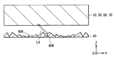
反射板40は、導光板10の背後から光変調素子30を介して漏れ出てきた光を導光板10側に戻すものである。反射板40は、例えば、反射、拡散、散乱などの機能を有している。これにより、光源20からの出射光を効率的に利用することができ、また、正面輝度の向上にも役立っている。反射板40の微細形状の表面は、鏡面となっていることが好ましい。この場合には、光変調層40からの出射光を正反射(鏡面反射)することができ、効率的に焦点C(後述)に反射することができる。反射板40は、例えば、発泡PET(ポリエチレンテレフタレート)や銀蒸着フィルム、多層膜反射フィルム、白色PETなどからなる。反射板40に正反射(鏡面反射)の機能を持たせる場合には、反射板40は、例えば、銀蒸着フィルム、多層膜反射フィルム、アルミニウム蒸着フィルムなどで構成されていることが好ましい。反射板40に微細形状を付与する場合は、反射板40は、熱可塑性樹脂を用いた熱プレス成型や溶融押し出し成型などの手法で一体的に形成されていてもよいし、また、例えばPETなどからなる基材上にエネルギー線(たとえば紫外線)硬化樹脂を塗布したのち、そのエネルギー線硬化樹脂に形状を転写して形成されていてもよい。ここで、熱可塑性樹脂としては、例えば、ポリカーボネート樹脂、PMMA(ポリメチルメタクリレート樹脂)などのアクリル樹脂、ポリエチレンテレフタレートなどのポリエステル樹脂、MS(メチルメタクリレートとスチレンの共重合体)などの非晶性共重合ポリエステル樹脂、ポリスチレン樹脂およびポリ塩化ビニル樹脂などが挙げられる。また、エネルギー線(たとえば紫外線)硬化樹脂に形状を転写する場合は、基材はガラスであってもよい。反射板40と光変調素子30の位置合わせが重要である場合には、反射板40と導光板10や透明基板31、透明基板37の材質は互いに同一であるか、もしくは線膨張係数の互いに近いものであることが好ましい。外温の変化や熱による位置ずれを防止するためである。   The reflection plate 40 returns light leaking from the back of the light guide plate 10 through the light modulation element 30 to the light guide plate 10 side. The reflector 40 has functions such as reflection, diffusion, and scattering. Thereby, the emitted light from the light source 20 can be used efficiently, and it is also useful for improving the front luminance. The finely shaped surface of the reflector 40 is preferably a mirror surface. In this case, the light emitted from the light modulation layer 40 can be regularly reflected (specular reflection), and can be efficiently reflected to the focal point C (described later). The reflection plate 40 is made of, for example, foamed PET (polyethylene terephthalate), a silver vapor deposition film, a multilayer film reflection film, white PET, or the like. In the case where the reflecting plate 40 has a function of regular reflection (specular reflection), the reflecting plate 40 is preferably composed of, for example, a silver vapor deposition film, a multilayer film reflection film, an aluminum vapor deposition film, or the like. When a fine shape is given to the reflector 40, the reflector 40 may be integrally formed by a technique such as hot press molding or melt extrusion molding using a thermoplastic resin. It may be formed by applying an energy ray (for example, ultraviolet ray) curable resin on a substrate made of the above, and then transferring the shape to the energy ray curable resin. Here, examples of the thermoplastic resin include polycarbonate resins, acrylic resins such as PMMA (polymethyl methacrylate resin), polyester resins such as polyethylene terephthalate, and amorphous copolymers such as MS (copolymer of methyl methacrylate and styrene). Examples thereof include a polymerized polyester resin, a polystyrene resin, and a polyvinyl chloride resin. Further, when the shape is transferred to an energy ray (for example, ultraviolet ray) curable resin, the substrate may be glass. When the alignment of the reflecting plate 40 and the light modulation element 30 is important, the materials of the reflecting plate 40, the light guide plate 10, the transparent substrate 31, and the transparent substrate 37 are the same or close to each other in linear expansion coefficient. It is preferable. This is to prevent a change in the external temperature and displacement due to heat.

反射板40は、例えば、図16に示したように、光変調層34の底面から距離H1だけ離れた位置に配置されており、光変調層34側に反射面40Aを有している。反射面40Aは、光源20からの出射光の一部を光出射面1Aの方へ反射するものである。より具体的には、反射板40は、表示装置において三次元表示を行うときに、散乱領域30Bにおいて生成される線状照明光を反射することにより、焦点を結ぶ反射光を生成するものである。   For example, as shown in FIG. 16, the reflection plate 40 is disposed at a position away from the bottom surface of the light modulation layer 34 by a distance H1, and has a reflection surface 40A on the light modulation layer 34 side. The reflecting surface 40A reflects a part of the light emitted from the light source 20 toward the light emitting surface 1A. More specifically, the reflective plate 40 generates reflected light that focuses on the reflective illumination by reflecting linear illumination light generated in the scattering region 30B when performing three-dimensional display on the display device. .

なお、反射板40は、表示装置において三次元表示を行うときに、散乱領域30Bにおいて生成される、複数の点状照明光の集合体である線状照明光を反射することにより、焦点を結ぶ反射光を生成するものであってもよい。また、反射板40は、表示装置において2視点から互いに異なる二次元映像を視認可能な二次元表示を行うときに、散乱領域30Bにおいて生成される点状照明光を反射することにより、焦点を結ぶ反射光を生成するものであってもよい。   Note that the reflector 40 is focused by reflecting linear illumination light, which is an aggregate of a plurality of point-like illumination lights, generated in the scattering region 30B when performing three-dimensional display on the display device. It may generate reflected light. In addition, the reflecting plate 40 focuses the light by reflecting the point illumination light generated in the scattering region 30B when performing two-dimensional display in which two-dimensional images different from each other can be viewed from two viewpoints on the display device. It may generate reflected light.

反射板40は、線状照明光を生成する部位(散乱領域30B)を通過する平面であって、かつ反射板40を含む平面と垂直な平面上またはその平面の近傍に反射光を反射するようになっている。より具体的には、反射板40は、線状照明光において、線状照明光を生成する部位(散乱領域30B)と垂直な平面と平行な光の成分を考えた場合に、線状照明光を生成する部位(散乱領域30B)を通過する線分であって、かつ反射板40を含む平面の法線と平行な線分の上またはその線分の近傍に焦点を結ぶ反射光を生成する凹凸形状を有している。さらに、反射板40は、線状照明光において、線状照明光を生成する部位(散乱領域30B)と垂直な平面と交差する光の成分を考えた場合に、線状照明光からの光を、線状照明光を生成する部位(散乱領域30B)またはその近傍に反射する凹凸形状を有している。ここで、反射面40Aが、生成された光を、その光が生成された方へ反射させるようになっている場合、これを式で表すと、例えば以下のようになる。つまり、反射板40は、2次元再帰性の反射の性質を有している。
反射前の光のベクトルV=(Vx,Vy,Vz)
反射後の光のベクトルV=(Vx,−Vy,−Vz)
The reflecting plate 40 is a plane that passes through a site (scattering region 30B) that generates linear illumination light, and reflects the reflected light on or near a plane that is perpendicular to the plane including the reflecting plate 40. It has become. More specifically, the reflecting plate 40 has a linear illumination light when considering a component of the linear illumination light that is parallel to a plane perpendicular to a portion (scattering region 30B) that generates the linear illumination light. Is generated on the line segment that passes through the region (scattering region 30B) that generates the light beam and is parallel to the normal line of the plane including the reflector 40, or in the vicinity of the line segment. It has an uneven shape. Further, the reflection plate 40, when considering the light component that intersects the plane perpendicular to the portion (scattering region 30B) that generates the linear illumination light in the linear illumination light, reflects the light from the linear illumination light. In addition, it has a concavo-convex shape that reflects at a site (scattering region 30B) that generates linear illumination light or in the vicinity thereof. Here, when the reflection surface 40A reflects the generated light toward the direction in which the light is generated, this can be expressed by the following formula, for example. That is, the reflector 40 has a two-dimensional recursive reflection property.
Vector of light before reflection V = (Vx, Vy, Vz)
Vector of reflected light V = (Vx, −Vy, −Vz)

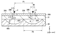
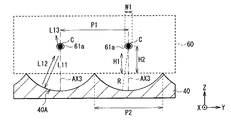
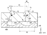
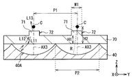
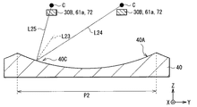
例えば、図16に示したように、線状照明光を生成する部位(散乱領域30B)と垂直な平面と平行な光の成分を考えた場合に、反射板40は、線分AX3の上またはその線分AX3の近傍であって、かつ散乱領域30Bの直下に反射光が焦点Cを結ぶ凹凸形状を有している。このとき、焦点Cの位置と、反射板40の上面との距離H2は、距離H1よりも短くなっており、(H1/n1−W1)以上、H1未満となっていることが好ましい。ここで、反射板40の上面とは、反射板40の上面に形成された複数の頂部を含む平面を指している。なお、W1は、線状照明光を生成する部位(散乱領域30B)の幅である。n1は、反射板40の上面と、焦点Cの位置との間の領域の屈折率であり、本実施の形態では透明基板31の屈折率である。AX3は、線状照明光を生成する部位(散乱領域30B)を通過する線分であって、かつ反射板40を含む平面の法線と平行な線分である。   For example, as illustrated in FIG. 16, when considering a light component parallel to a plane perpendicular to a portion that generates linear illumination light (scattering region 30 </ b> B), the reflecting plate 40 is placed on the line segment AX <b> 3 or In the vicinity of the line segment AX3 and directly under the scattering region 30B, the reflected light has an uneven shape that connects the focal point C. At this time, the distance H2 between the position of the focal point C and the upper surface of the reflecting plate 40 is shorter than the distance H1, and is preferably (H1 / n1-W1) or more and less than H1. Here, the upper surface of the reflecting plate 40 refers to a plane including a plurality of apexes formed on the upper surface of the reflecting plate 40. In addition, W1 is the width | variety of the site | part (scattering area | region 30B) which produces | generates linear illumination light. n1 is the refractive index of the region between the upper surface of the reflecting plate 40 and the position of the focal point C, and is the refractive index of the transparent substrate 31 in the present embodiment. AX3 is a line segment that passes through a portion (scattering region 30B) that generates linear illumination light, and is a line segment that is parallel to the normal line of the plane including the reflector 40.

なお、例えば、図17に示したように、線状照明光を生成する部位(散乱領域30B)と垂直な平面と平行な光の成分を考えた場合に、反射板40は、線分AX3の上またはその線分AX3の近傍であって、かつ散乱領域30Bの直上に反射光が焦点Cを結ぶ凹凸形状を有していてもよい。このとき、距離H2は、距離H1よりも長くなっており、H1よりも大きく、(H1/n1+W1)以下となっていることが好ましい。なお、例えば、図18に示したように、反射板40は、線分AX3の上またはその線分AX3の近傍であって、かつ散乱領域30B内に反射光が焦点Cを結ぶ凹凸形状を有していてもよい。このとき、距離H2は、距離H1と概ね等しくなる。   For example, as illustrated in FIG. 17, when considering a light component parallel to a plane perpendicular to a portion (scattering region 30 </ b> B) that generates linear illumination light, the reflector 40 has a line segment AX <b> 3. The reflection light may have an uneven shape that connects the focal point C on or near the line segment AX3 and directly above the scattering region 30B. At this time, it is preferable that the distance H2 is longer than the distance H1, larger than H1, and not more than (H1 / n1 + W1). For example, as shown in FIG. 18, the reflecting plate 40 has an uneven shape that is on or near the line segment AX3 and in which the reflected light has a focal point C in the scattering region 30B. You may do it. At this time, the distance H2 is substantially equal to the distance H1.

反射板40は、線状照明光を生成する部位(散乱領域30B)と対向する位置に、中心軸が焦点Cを通過する円柱の内面の一部を反射面40Aとして有している。反射面40Aは、散乱領域30Bと対向する位置が最も深くなっていることが好ましい。   The reflecting plate 40 has a part of the inner surface of a cylinder whose central axis passes through the focal point C as a reflecting surface 40A at a position facing the part (scattering region 30B) that generates linear illumination light. The reflecting surface 40A is preferably deepest at the position facing the scattering region 30B.

焦点Cの位置は、図16、図17、図18を比較した場合、図16に記載した位置(散乱領域30Bの直下)となっていることが最も良い。このとき、焦点Cの位置は、H2=H1/n1を満たす位置となっていることが最も良い。反射板40の反射面40Aにおける立体形状のピッチP2は、光変調層34内の散乱領域30B(線状照明光を生成する部位)のピッチP1と一致しているか、またはほぼ一致していることが最も良い。この場合に、さらに、反射面40Aのうち円柱の内面の一部に相当する部分の半径は、(H22+(P1/2)21/2となっていることが最も良い。このようにした場合には、反射面40Aで反射された光が、焦点Cに向かって進み、透明基板31の底面で屈折され、散乱領域30Bに再帰的に到達する。 When comparing FIG. 16, FIG. 17, and FIG. 18, the position of the focal point C is best at the position described in FIG. 16 (directly below the scattering region 30B). At this time, it is best that the position of the focal point C is a position that satisfies H2 = H1 / n1. The three-dimensional pitch P2 on the reflecting surface 40A of the reflecting plate 40 matches or substantially matches the pitch P1 of the scattering region 30B (part that generates linear illumination light) in the light modulation layer 34. Is the best. In this case, the radius of the portion corresponding to a part of the inner surface of the cylinder in the reflecting surface 40A is preferably (H2 2 + (P1 / 2) 2 ) 1/2 . In this case, the light reflected by the reflecting surface 40A travels toward the focal point C, is refracted at the bottom surface of the transparent substrate 31, and recursively reaches the scattering region 30B.

次に、反射板40によって生成される反射光の正面輝度分布および角度輝度分布について説明する。図19(A)は、光変調層34の散乱領域30Bから出射された光のうち光出射面1A側に出射された光L13の正面輝度分布および角度輝度分布の一例を表したものである。図19(B)は、光変調層34の散乱領域30Bから出射された光のうち光出射面1Aとは反対側に出射され、反射板40で反射された光L12の正面輝度分布および角度輝度分布の一例を表したものである。図19(A),(B)は、透明基板41の屈折率n=1.515、H1=700μm、H2=462μm(=H1/n)、焦点Cと反射面40Aとの距離(半径R)=526μm、P1=P2=504μm、W1=63μm、焦点Cが散乱領域30Bの直下にある、としたときの結果である。   Next, the front luminance distribution and the angular luminance distribution of the reflected light generated by the reflecting plate 40 will be described. FIG. 19A shows an example of the front luminance distribution and the angular luminance distribution of the light L13 emitted to the light emission surface 1A side of the light emitted from the scattering region 30B of the light modulation layer 34. FIG. FIG. 19B shows the front luminance distribution and angular luminance of the light L12 emitted from the scattering region 30B of the light modulation layer 34 to the side opposite to the light emitting surface 1A and reflected by the reflecting plate 40. An example of the distribution is shown. 19A and 19B show the refractive index n = 1.515 of the transparent substrate 41, H1 = 700 μm, H2 = 462 μm (= H1 / n), and the distance (radius R) between the focal point C and the reflecting surface 40A. = 526 μm, P1 = P2 = 504 μm, W1 = 63 μm, and the focal point C is directly below the scattering region 30B.

なお、図19(A),(B)の左側のグラフが正面輝度分布であり、図19(A),(B)の右側のグラフが角度輝度分布である。正面輝度分布とは、光変調層34の法線方向に出射される光の面内の輝度分布を指しており、横軸の原点が散乱領域30Bの直上に対応している。角度輝度分布とは、散乱領域30B内の面内中心点を通過した光のうち、光変調層34の法線方向に発散する光の輝度分布の角度分布を指しており、横軸の原点が光変調層34の法線方向に対応している。   19A and 19B are front luminance distributions, and the right graphs of FIGS. 19A and 19B are angular luminance distributions. The front luminance distribution refers to the luminance distribution in the plane of light emitted in the normal direction of the light modulation layer 34, and the origin of the horizontal axis corresponds to directly above the scattering region 30B. The angular luminance distribution refers to the angular distribution of the luminance distribution of light that diverges in the normal direction of the light modulation layer 34 among the light that has passed through the in-plane center point in the scattering region 30B, and the origin of the horizontal axis is This corresponds to the normal direction of the light modulation layer 34.

図19(A),(B)から、光L12の正面輝度分布および角度輝度分布は、光L13の正面輝度分布および角度輝度分布と同一またはほぼ同一となっていることがわかる。つまり、反射板40は、散乱領域30Bから光出射面1A側に出力される光の正面輝度分布および角度輝度分布をほとんど崩すことなく、光L13を散乱領域30Bに戻している。これは、反射光が光変調素子34の透過領域30Aに入射する割合を小さくすることができるという効果だけでなく、三次元表示に必要のない角度方向に出射する光を増やさないという効果もあることを意味している。   19A and 19B, it can be seen that the front luminance distribution and the angular luminance distribution of the light L12 are the same as or substantially the same as the front luminance distribution and the angular luminance distribution of the light L13. That is, the reflector 40 returns the light L13 to the scattering region 30B without substantially destroying the front luminance distribution and the angular luminance distribution of the light output from the scattering region 30B to the light exit surface 1A side. This not only has the effect of reducing the rate at which the reflected light is incident on the transmission region 30A of the light modulation element 34, but also has the effect of not increasing the light emitted in the angular direction that is not necessary for three-dimensional display. It means that.

図20は、比較例に係る反射板41を、光源21と共に模式的に表したものである。反射板41は、光源21からの光を反射して平行光を生成する放物面を有している。図20において、光源21から上方に直接に出射された光が光L16であり、光源21から反射板41側に出射された光が光L14であり、光L14のうち反射板41で反射された光が光L15である。図21(A)は、光L16の正面輝度分布および角度輝度分布の一例を表したものである。図21(B)は、光L15の正面輝度分布および角度輝度分布の一例を表したものである。なお、図21(A),(B)の左側のグラフが正面輝度分布であり、図21(A),(B)の右側のグラフが角度輝度分布である。   FIG. 20 schematically illustrates the reflector 41 according to the comparative example together with the light source 21. The reflection plate 41 has a paraboloid that reflects the light from the light source 21 to generate parallel light. In FIG. 20, the light directly emitted upward from the light source 21 is the light L16, the light emitted from the light source 21 to the reflection plate 41 side is the light L14, and the light L14 is reflected by the reflection plate 41. The light is light L15. FIG. 21A shows an example of the front luminance distribution and the angular luminance distribution of the light L16. FIG. 21B shows an example of the front luminance distribution and the angular luminance distribution of the light L15. 21A and 21B are front luminance distributions, and the right graphs of FIGS. 21A and 21B are angular luminance distributions.

図21(A),(B)から、光L15の正面輝度分布および角度輝度分布が、光L16の正面輝度分布および角度輝度分布とは全く異なっていることがわかる。光L15の正面輝度分布は、面内の場所によらずおおむね一定となっており、光L15が光変調素子34の透過領域30Aにかなりの割合で入射している。また、光L15の角度輝度分布が正面方向に大きく偏っており、三次元表示の際に表示品質の低下が懸念される。   21A and 21B that the front luminance distribution and the angular luminance distribution of the light L15 are completely different from the front luminance distribution and the angular luminance distribution of the light L16. The front luminance distribution of the light L15 is generally constant regardless of the location in the plane, and the light L15 is incident on the transmission region 30A of the light modulation element 34 at a considerable rate. In addition, the angular luminance distribution of the light L15 is greatly deviated in the front direction, and there is a concern that display quality may deteriorate during three-dimensional display.

図22は、比較例に係る反射板42を、光源21と共に模式的に表したものである。反射板42は、光源21からの光を正反射する平坦面を有している。図22において、光源21から上方に直接に出射された光が光L16であり、光源21から反射板42側に出射された光のうち反射板42で正反射された光が光L17である。図23(A)は、光L16の正面輝度分布および角度輝度分布の一例を表したものである。図23(B)は、光L17の正面輝度分布および角度輝度分布の一例を表したものである。なお、図23(A),(B)の左側のグラフが正面輝度分布であり、図23(A),(B)の右側のグラフが角度輝度分布である。   FIG. 22 schematically shows the reflector 42 according to the comparative example together with the light source 21. The reflection plate 42 has a flat surface that regularly reflects light from the light source 21. In FIG. 22, the light directly emitted upward from the light source 21 is the light L16, and the light regularly reflected by the reflection plate 42 among the light emitted from the light source 21 to the reflection plate 42 side is the light L17. FIG. 23A shows an example of the front luminance distribution and the angular luminance distribution of the light L16. FIG. 23B shows an example of the front luminance distribution and the angular luminance distribution of the light L17. Note that the left graphs of FIGS. 23A and 23B are front luminance distributions, and the right graphs of FIGS. 23A and 23B are angular luminance distributions.

図23(A),(B)から、光L17の正面輝度分布および角度輝度分布が、光L16の正面輝度分布および角度輝度分布とは全く異なっていることがわかる。光L17の正面輝度分布は、正面方向にピークを持っているが、正面方向以外の方向にも大きな成分を持っており、光L17が光変調素子34の透過領域30Aにかなりの割合で入射している。また、光L17の角度輝度分布が角度によらず一定となっており、三次元表示の際に表示品質の低下が懸念される。   23A and 23B, it can be seen that the front luminance distribution and the angular luminance distribution of the light L17 are completely different from the front luminance distribution and the angular luminance distribution of the light L16. The front luminance distribution of the light L17 has a peak in the front direction, but has a large component in directions other than the front direction, and the light L17 is incident on the transmission region 30A of the light modulation element 34 at a considerable rate. ing. In addition, the angular luminance distribution of the light L17 is constant regardless of the angle, and there is a concern that display quality may deteriorate during three-dimensional display.

なお、本実施の形態において、反射板40は透明基板31と接着されていてもよい。反射板40と透明基板31との接着には、全面接着、外周部分の接着(表示領域以外の部分を環状に接着)、または点状接着(表示領域以外の部分を点状に接着)が考えられる。反射板40と透明基板31とを全面接着する場合には、反射板40の頂点部分を透明基板31に接着することが考えられる。このとき、反射板40の頂点部分が、若干の平坦面となっていてもよい。   In the present embodiment, the reflection plate 40 may be bonded to the transparent substrate 31. Adhesion between the reflecting plate 40 and the transparent substrate 31 may be whole surface adhesion, adhesion of the outer peripheral portion (a portion other than the display region is adhered in a ring shape), or point-like adhesion (a portion other than the display region is adhered in a dot shape). It is done. In the case where the reflection plate 40 and the transparent substrate 31 are bonded together over the entire surface, it is conceivable that the apex portion of the reflection plate 40 is bonded to the transparent substrate 31. At this time, the apex portion of the reflecting plate 40 may be a slightly flat surface.

また、本実施の形態において、反射板40は、例えば、図24に示したように、透明基板31と接する部位にブラック43を有していてもよい。このブラック43は、例えば、反射板40を透明基板31の裏面に固定する接着剤に黒色の顔料を混ぜたものであってもよい。   Moreover, in this Embodiment, the reflecting plate 40 may have the black 43 in the site | part which contact | connects the transparent substrate 31, for example, as shown in FIG. The black 43 may be, for example, a black pigment mixed with an adhesive that fixes the reflective plate 40 to the back surface of the transparent substrate 31.

以下に、本実施の形態の照明装置1の製造方法について、図25(A)〜(C)から図27(A)〜(C)を参照しながら説明する。   Below, the manufacturing method of the illuminating device 1 of this Embodiment is demonstrated, referring FIG. 25 (A)-(C) to FIG. 27 (A)-(C).

まず、ガラス基板またはプラスチックフィルム基板からなる透明基板31上に、ITOなどの透明導電膜32Eを形成する(23(A))。次に、表面全体にレジスト層を形成したのち、パターニングによりレジスト層に電極パターンを形成する。続いて、露光、現像により下側電極32を形成し、レジスト層を除去する(図25(B))。   First, a transparent conductive film 32E such as ITO is formed on a transparent substrate 31 made of a glass substrate or a plastic film substrate (23 (A)). Next, after forming a resist layer on the entire surface, an electrode pattern is formed on the resist layer by patterning. Subsequently, the lower electrode 32 is formed by exposure and development, and the resist layer is removed (FIG. 25B).

パターニングの方法としては、例えば、フォトリソグラフィ法、レーザー加工法、パターン印刷法、スクリーン印刷法などを用いることが可能である。また、例えば、メルク社の"ハイパーエッチ"材料を用いてスクリーン印刷した後に所定の加熱を行い、その後、水洗することでパターニングを行うこともできる。電極パターンは駆動方法および部分駆動の分割数によって決定される。電極パターンは、例えば、使用する表示装置の画素ピッチか、それに近いピッチで加工される。電極の加工幅は、加工方法にも依存するが、光りの取り出し効率という観点においてできるだけ細いことが好ましい。電極の加工幅は、例えば、50μm以下、好ましくは20μm、さらに好ましくは5μm以下である。また、ITOナノ粒子をパターン印刷した後、それを焼成することによって電極パターンを形成してもよい。   As a patterning method, for example, a photolithography method, a laser processing method, a pattern printing method, a screen printing method, or the like can be used. Also, for example, patterning can be performed by performing predetermined heating after screen printing using a “Hyper Etch” material manufactured by Merck and then washing with water. The electrode pattern is determined by the driving method and the number of divisions for partial driving. The electrode pattern is processed at, for example, a pixel pitch of a display device to be used or a pitch close thereto. The processing width of the electrode depends on the processing method, but is preferably as thin as possible from the viewpoint of light extraction efficiency. The processing width of the electrode is, for example, 50 μm or less, preferably 20 μm, and more preferably 5 μm or less. Moreover, you may form an electrode pattern by baking ITO nanoparticle after pattern printing.

次に、表面全体に配向膜33を塗布したのち、乾燥させ、焼成する(図25(C))。配向膜33としてポリイミド系材料を用いる場合には、溶媒にNMP(N−メチル−2−ピロリドン)を用いることが多いが、そのときには、大気下では200℃程度の温度が必要である。なお、この場合に、透明基板31としてプラスチック基板を用いる場合には、配向膜33を100℃で真空乾燥させ、焼成することもできる。その後、配向膜33に対してラビング処理を行う。これにより、配向膜33が水平配向用の配向膜として機能し、さらに配向膜33のラビング方向にプレチルトを形成することが可能となる。   Next, after the alignment film 33 is applied to the entire surface, it is dried and baked (FIG. 25C). When a polyimide-based material is used as the alignment film 33, NMP (N-methyl-2-pyrrolidone) is often used as a solvent. At that time, a temperature of about 200 ° C. is required in the atmosphere. In this case, when a plastic substrate is used as the transparent substrate 31, the alignment film 33 can be vacuum-dried at 100 ° C. and fired. Thereafter, the alignment film 33 is rubbed. As a result, the alignment film 33 functions as an alignment film for horizontal alignment, and a pretilt can be formed in the rubbing direction of the alignment film 33.

同様にして、ガラス基板またはプラスチックフィルム基板からなる透明基板37上に、ITOなどの透明導電膜を形成する。次に、表面全体にレジスト層を形成したのち、パターニングによりレジスト層に電極パターンを形成する。続いて、露光、現像により上側電極36を形成し、レジスト層を除去する。次に、表面全体に配向膜35を塗布したのち、乾燥させ、焼成する。その後、配向膜35に対してラビング処理を行う。これにより、配向膜35が水平配向用の配向膜として機能し、さらに配向膜35のラビング方向にプレチルトを形成することが可能となる。   Similarly, a transparent conductive film such as ITO is formed on a transparent substrate 37 made of a glass substrate or a plastic film substrate. Next, after forming a resist layer on the entire surface, an electrode pattern is formed on the resist layer by patterning. Subsequently, the upper electrode 36 is formed by exposure and development, and the resist layer is removed. Next, after the alignment film 35 is applied to the entire surface, it is dried and baked. Thereafter, a rubbing process is performed on the alignment film 35. As a result, the alignment film 35 functions as an alignment film for horizontal alignment, and a pretilt can be formed in the rubbing direction of the alignment film 35.

次に、配向膜33上に、セルギャップを形成するためのスペーサ38を乾式または湿式で散布する(図26(A))。なお、真空貼り合わせ法にて光変調セル30−1を作成する場合には、滴下する混合物中にスペーサ38を混合しておいてもよい。また、スペーサ38の替わりとして、フォトリソ法によって柱スペーサを形成することもできる。続いて、配向膜35上に、貼り合わせおよび液晶の漏れを防止するためのシール剤パターン39を、例えば額縁状に塗布する(図26(B))。このシール剤パターン39はディスペンサー法やスクリーン印刷法にて形成することができる。   Next, spacers 38 for forming a cell gap are sprayed on the alignment film 33 in a dry or wet manner (FIG. 26A). In addition, when producing the light modulation cell 30-1 by the vacuum bonding method, the spacer 38 may be mixed in the mixture to be dropped. Further, instead of the spacer 38, a column spacer can be formed by photolithography. Subsequently, a sealant pattern 39 for preventing bonding and liquid crystal leakage is applied onto the alignment film 35 in a frame shape, for example (FIG. 26B). The sealant pattern 39 can be formed by a dispenser method or a screen printing method.

以下に、真空貼り合わせ法(One Drop Fill法、ODF法)について説明するが、真空注入法やロール貼合方式などで光変調セル30−1を作成することも可能である。   Although the vacuum bonding method (One Drop Fill method, ODF method) is demonstrated below, it is also possible to create the light modulation cell 30-1 by a vacuum injection method, a roll bonding method, etc.

まず、セルギャップ、セル面積などから決まる体積分にあたる液晶とモノマーの混合物44を面内に均一に滴下する(図26(C))。混合物44の滴下にはリニアガイド方式の精密ディスペンサーを用いることが好ましいが、シール剤パターン39を土手として利用して、ダイコータなどを用いてもよい。   First, a liquid crystal / monomer mixture 44 corresponding to a volume determined by a cell gap, a cell area, and the like is uniformly dropped in a plane (FIG. 26C). A linear guide precision dispenser is preferably used for dropping the mixture 44, but a die coater or the like may be used by using the sealant pattern 39 as a bank.

液晶とモノマーは前述の材料を用いることができるが、液晶とモノマーの重量比は98:2〜50:50、好ましくは95:5〜75:25、より好ましくは92:8〜85:15である。液晶の比率を多くすることで駆動電圧を低くすることができるが、あまり液晶を多くしすぎると電圧印加時の白色度が低下したり、電圧オフ後に応答速度が低下するなど透明時に戻りにくくなったりする傾向がある。   The above-mentioned materials can be used for the liquid crystal and the monomer, but the weight ratio of the liquid crystal to the monomer is 98: 2 to 50:50, preferably 95: 5 to 75:25, more preferably 92: 8 to 85:15. is there. The drive voltage can be lowered by increasing the ratio of the liquid crystal, but if too much liquid crystal is added too much, the whiteness at the time of voltage application will decrease or the response speed will decrease after the voltage is turned off, making it difficult to return to transparency. There is a tendency to.

混合物44には、液晶とモノマーの他には、重合開始剤を添加する。使用する紫外線波長に応じて、添加する重合開始剤のモノマー比を0.1〜10重量%の範囲内で調整する。混合物42には、この他に、重合禁止剤や可塑剤、粘度調整剤なども必要に応じて添加可能である。モノマーが室温で固体やゲル状である場合には、口金やシリンジ、基板を加温することが好ましい。   In addition to the liquid crystal and the monomer, a polymerization initiator is added to the mixture 44. The monomer ratio of the polymerization initiator to be added is adjusted within a range of 0.1 to 10% by weight depending on the ultraviolet wavelength used. In addition to this, a polymerization inhibitor, a plasticizer, a viscosity modifier and the like can be added to the mixture 42 as necessary. When the monomer is solid or gelled at room temperature, it is preferable to heat the base, syringe, and substrate.

透明基板31および透明基板37を真空貼り合わせ機(図示せず)に配置したのち、真空排気し、貼り合わせを行う(図27(A))。その後、貼り合わせたものを大気に解放し、大気圧での均一加圧によってセルギャップを均一化する。セルギャップは白輝度(白色度)と駆動電圧の関係から適宜選定できるが、5〜40μm、好ましくは6〜20μm、より好ましくは7〜10μmである。   After the transparent substrate 31 and the transparent substrate 37 are placed in a vacuum bonding machine (not shown), they are evacuated and bonded (FIG. 27A). Thereafter, the bonded material is released to the atmosphere, and the cell gap is made uniform by uniform pressurization at atmospheric pressure. The cell gap can be appropriately selected from the relationship between the white luminance (whiteness) and the driving voltage, and is 5 to 40 μm, preferably 6 to 20 μm, more preferably 7 to 10 μm.

貼り合わせ後、必要に応じて配向処理を行うことが好ましい(図示せず)。クロスニコル偏光板の間に、貼り合わせたセルを挿入した際に、光り漏れが生じている場合には、セルをある一定時間加熱処理したり、室温で放置したりして配向させる。その後、紫外線L3を照射してモノマーを重合させてポリマー化する(図27(B))。このようにして、光変調素子30が製造される。   After bonding, it is preferable to perform an alignment treatment as necessary (not shown). If light leakage occurs when the bonded cells are inserted between the crossed Nicols polarizing plates, the cells are oriented by heat treatment for a certain period of time or by leaving them at room temperature. Then, the monomer is polymerized by irradiating with ultraviolet rays L3 to form a polymer (FIG. 27B). In this way, the light modulation element 30 is manufactured.

紫外線を照射している時には、セルの温度が変化しないようにすることが好ましい。赤外線カットフィルターを用いたり、光源にUV−LEDなどを用いたりすることが好ましい。紫外線照度は複合材料の組織構造に影響を与えるので、使用する液晶材料やモノマー材料、これらの組成から適宜調整することが好ましく、0.1〜500mW/cm2の範囲が好ましく、さらに好ましくは0.5〜30mW/cm2である。紫外線照度が低いほど駆動電圧が低くなる傾向にあり、生産性と特性の両面から好ましい紫外線照度を選定することができる。 It is preferable that the temperature of the cell does not change during irradiation with ultraviolet rays. It is preferable to use an infrared cut filter or a UV-LED as a light source. Since the ultraviolet illuminance affects the structure of the composite material, it is preferably adjusted as appropriate from the liquid crystal material and monomer material used, and their composition, preferably in the range of 0.1 to 500 mW / cm 2 , more preferably 0. 5 to 30 mW / cm 2 . The driving voltage tends to be lower as the ultraviolet illuminance is lower, and a preferable ultraviolet illuminance can be selected from both aspects of productivity and characteristics.

そして、導光板10に光変調素子30を貼り合わせる(図27(C))。貼り合わせには、粘着、接着のいずれでもよいが、導光板10の屈折率と光変調素子30の基板材料の屈折率とにできるだけ近い屈折率の材料で粘着、接着することが好ましい。最後に、下側電極32および上側電極36に引き出し線(図示せず)を取り付ける。このようにして、本実施の形態の照明装置1が製造される。   Then, the light modulation element 30 is bonded to the light guide plate 10 (FIG. 27C). For the bonding, either adhesion or adhesion may be used, but adhesion and adhesion are preferably performed using a material having a refractive index as close as possible to the refractive index of the light guide plate 10 and the refractive index of the substrate material of the light modulation element 30. Finally, lead wires (not shown) are attached to the lower electrode 32 and the upper electrode 36. In this way, the lighting device 1 of the present embodiment is manufactured.

このように、光変調素子30を作成し、最後に導光板10に光変調素子30を貼り合わせるプロセスを説明したが、導光板10の表面に、配向膜35を形成した透明基板37を予め貼り合わせてから、照明装置1を作成することもできる。また、枚葉方式、ロール・ツー・ロール方式のいずれでも照明装置1を作成することができる。   As described above, the process of creating the light modulation element 30 and finally bonding the light modulation element 30 to the light guide plate 10 has been described. However, the transparent substrate 37 on which the alignment film 35 is formed is pasted on the surface of the light guide plate 10 in advance. The lighting device 1 can also be created after matching. Moreover, the illuminating device 1 can be produced by either a single wafer method or a roll-to-roll method.

次に、本実施の形態の照明装置1の作用および効果について説明する。   Next, the operation and effect of the illumination device 1 of the present embodiment will be described.

本実施の形態の照明装置1では、三次元表示のときに、各セル30aにおいて微粒子34Bの光軸AX2がバルク34Aの光軸AX1と交差もしくは直交し、各セル30bにおいて微粒子34Bの光軸AX2がバルク34Aの光軸AX1と平行もしくはほぼ平行となるように、各光変調セル30−1の一対の電極(部分電極32A、上側電極36)に電圧が印加される。これにより、光変調素子30において、各セル30aが散乱領域30Bとなり、各セル30bが透過領域30Aとなる。その結果、光源20から出射され、導光板10内に入射した光は、光変調素子30のうち透過領域30Aを透過し、光変調素子30のうち散乱領域30Bにおいて散乱される(図14)。この散乱光のうち散乱領域30Bの下面を透過した光は反射板40で反射され、再度、導光板10に戻されたのち、照明装置1の上面から出射される。また、散乱光のうち、散乱領域30Bの上面に向かった光は、導光板10を透過したのち、照明装置1の上面から出射される。このように、三次元表示のときには、透過領域30Aの上面からは光はほとんど出射されず、散乱領域30Bの上面から光が出射される。このようにして、例えば、図14に示したように、正面方向に線状照明光が出力される。   In the illumination device 1 according to the present embodiment, the optical axis AX2 of the fine particles 34B intersects or is orthogonal to the optical axis AX1 of the bulk 34A in each cell 30a and the optical axis AX2 of the fine particles 34B in each cell 30b during three-dimensional display. Is applied to the pair of electrodes (partial electrode 32A, upper electrode 36) of each light modulation cell 30-1 such that is parallel or substantially parallel to the optical axis AX1 of the bulk 34A. Thereby, in the light modulation element 30, each cell 30a becomes the scattering region 30B, and each cell 30b becomes the transmission region 30A. As a result, the light emitted from the light source 20 and entering the light guide plate 10 is transmitted through the transmission region 30A of the light modulation element 30, and is scattered in the scattering region 30B of the light modulation element 30 (FIG. 14). Of this scattered light, the light transmitted through the lower surface of the scattering region 30 </ b> B is reflected by the reflecting plate 40, returned again to the light guide plate 10, and then emitted from the upper surface of the lighting device 1. In addition, light scattered toward the upper surface of the scattering region 30 </ b> B is emitted from the upper surface of the illumination device 1 after passing through the light guide plate 10. As described above, in the three-dimensional display, light is hardly emitted from the upper surface of the transmission region 30A, and light is emitted from the upper surface of the scattering region 30B. In this way, for example, as shown in FIG. 14, linear illumination light is output in the front direction.

また、本実施の形態の照明装置1では、二次元表示のときに、例えば、各光変調セル30−1において微粒子34Bの光軸AX2がバルク34Aの光軸AX1と交差もしくは直交するように、各光変調セル30−1の一対の電極(部分電極32A、上側電極36)に電圧が印加される。これにより、光源20から出射され、導光板10内に入射した光は、光変調素子30の全体に形成された散乱領域30Bにおいて散乱される。この散乱光のうち散乱領域30Bの下面を透過した光は反射板40で反射され、再度、導光板10に戻されたのち、照明装置1の上面から出射される。また、散乱光のうち、散乱領域30Bの上面に向かった光は、導光板10を透過したのち、照明装置1の上面から出射される。このように、二次表示のときには、例えば、光変調素子30の上面全体から光が出射され、正面方向に、面状照明光が出力される。   Further, in the illumination device 1 of the present embodiment, for two-dimensional display, for example, in each light modulation cell 30-1, the optical axis AX2 of the fine particles 34B intersects or is orthogonal to the optical axis AX1 of the bulk 34A. A voltage is applied to a pair of electrodes (partial electrode 32A, upper electrode 36) of each light modulation cell 30-1. Thereby, the light emitted from the light source 20 and incident into the light guide plate 10 is scattered in the scattering region 30 </ b> B formed in the entire light modulation element 30. Of this scattered light, the light transmitted through the lower surface of the scattering region 30 </ b> B is reflected by the reflecting plate 40, returned again to the light guide plate 10, and then emitted from the upper surface of the lighting device 1. In addition, light scattered toward the upper surface of the scattering region 30 </ b> B is emitted from the upper surface of the illumination device 1 after passing through the light guide plate 10. Thus, at the time of secondary display, for example, light is emitted from the entire top surface of the light modulation element 30, and planar illumination light is output in the front direction.

ところで、本実施の形態では、三次元表示に際して、パララックスバリアを設ける必要がない。また、仮に、パララックスバリアを、照明装置1の光出射側に設けたとしても、そのときに、光変調層34の一部を散乱領域30Bとし、その散乱領域30Bをパララックスバリアの光透過領域に対応させることで、光変調層34から出力された光がパララックスバリアで吸収される割合を極めて低くすることができる。また、本実施の形態では、三次元表示に際して、シリンドリカルレンズを必要としないので、シリンドリカルレンズに起因する収差の問題が生じる虞はない。   By the way, in this embodiment, it is not necessary to provide a parallax barrier for three-dimensional display. Even if the parallax barrier is provided on the light emitting side of the lighting device 1, a part of the light modulation layer 34 is used as the scattering region 30B and the scattering region 30B is transmitted through the parallax barrier. By making it correspond to a region, the ratio of the light output from the light modulation layer 34 absorbed by the parallax barrier can be extremely reduced. In this embodiment, since a cylindrical lens is not required for three-dimensional display, there is no possibility that an aberration problem caused by the cylindrical lens occurs.

また、本実施の形態では、線状照明光のうち反射板40側に出射した光が反射板40で反射されることにより、焦点を結ぶ反射光L12が生成される。これにより、反射光L12の正面強度分布および角度強度分布を、線状照明光のうち反射板40とは反対側に出射した光L13の正面強度分布および角度強度分布に近づけることができる。その結果、反射板の上面を平坦面で構成した場合(図22参照)や、平行光を生成する放物曲面で構成した場合(図20参照)と比べて、三次元表示の際に、反射光L13が散乱領域30Bとは異なる領域(つまり透過領域30A)を通過して上面から出射される割合を減らすことができる。さらに、反射光L12が三次元表示に必要のない角度方向に出射される割合を少なくすることもできる。これにより、このような照明装置1を三次元表示用の表示装置のバックライトとして適用した場合に、三次元表示における二重像の生成を低減することができる。従って、三次元表示における表示品質が向上する。   Moreover, in this Embodiment, the reflected light L12 which forms a focus is produced | generated by the light radiate | emitted to the reflecting plate 40 side among linear illumination lights being reflected by the reflecting plate 40. FIG. Thereby, the front intensity distribution and the angular intensity distribution of the reflected light L12 can be brought close to the front intensity distribution and the angular intensity distribution of the light L13 emitted to the side opposite to the reflecting plate 40 in the linear illumination light. As a result, compared with the case where the upper surface of the reflecting plate is configured as a flat surface (see FIG. 22) and the case where it is configured as a parabolic curved surface that generates parallel light (see FIG. 20), reflection is performed in three-dimensional display. The ratio at which the light L13 is emitted from the upper surface through a region different from the scattering region 30B (that is, the transmission region 30A) can be reduced. Further, the ratio of the reflected light L12 emitted in the angular direction that is not necessary for the three-dimensional display can be reduced. Thereby, when such an illuminating device 1 is applied as a backlight of a display device for three-dimensional display, generation of a double image in three-dimensional display can be reduced. Therefore, the display quality in the three-dimensional display is improved.

次に、本実施の形態の照明装置1の他の効果について説明する。   Next, another effect of the lighting device 1 according to the present embodiment will be described.

一般に、PDLCは、液晶材料と等方性の低分子材料とを混合し、紫外線照射や溶媒の乾燥などにより相分離を起こさせることによって形成され、液晶材料の微小粒子が高分子材料中に分散された複合層となっている。この複合層中の液晶材料は、電圧無印加時にはランダムな方向を向いているので散乱性を示すが、電圧印加時には電場方向に配向するので、液晶材料の常光屈折率と高分子材料の屈折率とが互いに等しい場合には、正面方向(PDLCの法線方向)において高い透明性を示す。しかし、この液晶材料では、斜め方向においては、液晶材料の異常光屈折率と高分子材料の屈折率との差が顕著となり、正面方向が透明性であっても斜め方向において散乱性が発現してしまう。   In general, PDLC is formed by mixing liquid crystal material and isotropic low molecular weight material and causing phase separation by ultraviolet irradiation or solvent drying, and the fine particles of liquid crystal material are dispersed in the polymer material. It is a composite layer. The liquid crystal material in this composite layer is scattered in a random direction when no voltage is applied, but is oriented in the direction of the electric field when a voltage is applied, so the normal refractive index of the liquid crystal material and the refractive index of the polymer material Are equal to each other, high transparency is exhibited in the front direction (normal direction of PDLC). However, in this liquid crystal material, the difference between the extraordinary refractive index of the liquid crystal material and the refractive index of the polymer material becomes significant in the oblique direction, and even if the front direction is transparent, the scattering property is exhibited in the oblique direction. End up.

通常、PDLCを使った光変調素子は、表面に透明導電膜の形成された2枚のガラス板の間にPDLCを挟み込んだ構造となっていることが多い。上述したような構造を有する光変調素子に対して空気中から斜めに光が入射した場合には、その斜め方向から入射した光は空気とガラス板の屈折率差によって屈折し、より小さな角度でPDLCに入射することになる。そのため、このような光変調素子においては、大きな散乱は生じない。例えば、空気中から80°の角度で光が入射した場合には、その光のPDLCへの入射角はガラス界面での屈折によって40°程度にまで小さくなる。   Usually, a light modulation element using PDLC often has a structure in which PDLC is sandwiched between two glass plates having a transparent conductive film formed on the surface thereof. When light is incident obliquely from the air on the light modulation element having the structure as described above, the light incident from the oblique direction is refracted by the difference in refractive index between the air and the glass plate, and at a smaller angle. The light enters the PDLC. Therefore, no large scattering occurs in such a light modulation element. For example, when light is incident from the air at an angle of 80 °, the incident angle of the light on the PDLC is reduced to about 40 ° due to refraction at the glass interface.

しかし、導光板を用いたエッジライト方式では、導光板越しに光が入射するので、光が80°程度の大きな角度でPDLC中を横切ることになる。そのため、液晶材料の異常光屈折率と高分子材料の屈折率との差が大きく、さらに、より大きな角度で光がPDLC中を横切るので、散乱を受ける光路も長くなる。例えば、常光屈折率1.5、異常光屈折率1.65の液晶材料の微小粒子が屈折率1.5の高分子材料中に分散されている場合には、正面方向(PDLCの法線方向)においては屈折率差がないが、斜め方向においては屈折率差が大きくなる。このため、斜め方向の散乱性を小さくすることができないので、視野角特性が悪い。さらに、導光板上に拡散フィルムなどの光学フィルムを設けた場合には、斜め漏れ光が拡散フィルムなどによって正面方向にも拡散されるので、正面方向の光漏れが大きくなり、正面方向の変調比が低くなってしまう。   However, in the edge light system using the light guide plate, light enters through the light guide plate, so that light crosses the PDLC at a large angle of about 80 °. For this reason, the difference between the extraordinary refractive index of the liquid crystal material and the refractive index of the polymer material is large, and furthermore, since the light crosses the PDLC at a larger angle, the optical path that receives the scattering becomes longer. For example, when fine particles of a liquid crystal material having an ordinary light refractive index of 1.5 and an extraordinary light refractive index of 1.65 are dispersed in a polymer material having a refractive index of 1.5, the front direction (the normal direction of the PDLC) ), There is no difference in refractive index, but the difference in refractive index increases in the oblique direction. For this reason, since the scattering property in the oblique direction cannot be reduced, the viewing angle characteristics are poor. In addition, when an optical film such as a diffusion film is provided on the light guide plate, oblique leakage light is also diffused in the front direction by the diffusion film, etc., so that light leakage in the front direction increases, and the modulation ratio in the front direction is increased. Will be lower.

一方、本実施の形態では、バルク34Aおよび微粒子34Bが光学異方性材料を主に含んで形成されているので、斜め方向において、散乱性が小さくなり、透明性を向上させることができる。例えば、バルク34Aおよび微粒子34Bが、互いに常光屈折率が等しく、かつ互いに異常光屈折率も等しい光学異方性材料を主に含んで構成され、かつ、下側電極32および上側電極36間に電圧が印加されていない領域では、これらの光軸の向きが一致もしくはほぼ一致する。これにより、正面方向(光変調素子30の法線方向)および斜め方向を含むあらゆる方向において屈折率差が少なくなるか、またはなくなり、高い透明性が得られる。その結果、視野角の大きい範囲における光の漏洩を低減またはほとんどなくすることができ、視野角特性を良くすることができる。   On the other hand, in the present embodiment, since the bulk 34A and the fine particles 34B are mainly formed of an optically anisotropic material, the scattering property is reduced in the oblique direction, and the transparency can be improved. For example, the bulk 34 </ b> A and the fine particles 34 </ b> B mainly include optically anisotropic materials having the same ordinary light refractive index and the same extraordinary light refractive index, and a voltage between the lower electrode 32 and the upper electrode 36. In the region where no is applied, the directions of these optical axes coincide or substantially coincide. Thereby, the refractive index difference is reduced or eliminated in all directions including the front direction (normal direction of the light modulation element 30) and the oblique direction, and high transparency is obtained. As a result, light leakage in a range with a large viewing angle can be reduced or almost eliminated, and viewing angle characteristics can be improved.

例えば、常光屈折率1.5、異常光屈折率1.65の液晶と、常光屈折率1.5、異常光屈折率1.65の液晶性モノマーとを混合し、配向膜または電界によって液晶と液晶性モノマーを配向させた状態で液晶性モノマーを重合させると、液晶の光軸と、液晶性モノマーが重合することによって形成されたポリマーの光軸とが互いに一致する。これにより、あらゆる方向で屈折率を一致させることができるので、そのようにした場合には、透明性が高い状態を実現でき、より一層、視野角特性を良くすることができる。   For example, a liquid crystal having an ordinary light refractive index of 1.5 and an extraordinary light refractive index of 1.65 is mixed with a liquid crystalline monomer having an ordinary light refractive index of 1.5 and an extraordinary light refractive index of 1.65, and the liquid crystal is formed by an alignment film or an electric field. When the liquid crystalline monomer is polymerized in a state where the liquid crystalline monomer is aligned, the optical axis of the liquid crystal and the optical axis of the polymer formed by polymerizing the liquid crystalline monomer coincide with each other. Thereby, since the refractive index can be matched in all directions, in such a case, a highly transparent state can be realized, and the viewing angle characteristics can be further improved.

また、本実施の形態では、例えば、図14(A),(B)に示したように、透過領域30Aの輝度(黒表示の輝度)が、全面を均一に発光させた場合(図14(B)中の一点鎖線)と比べて下がっている。他方、散乱領域30Bの輝度は、全面を均一に発光させた場合(図14(B)中の一点鎖線)と比べて極めて高くなり、しかも、透過領域30Aの輝度が低下した分だけ、部分的な白表示の輝度(輝度突き上げ)が大きくなる。   In this embodiment, for example, as shown in FIGS. 14A and 14B, the luminance of the transmissive region 30A (black display luminance) is uniformly emitted over the entire surface (FIG. It is lower than the one-dot chain line in B). On the other hand, the brightness of the scattering region 30B is extremely higher than that when the entire surface is made to emit light uniformly (dashed line in FIG. 14B), and the brightness of the transmission region 30A is partially reduced. The brightness of bright white display (increased brightness) increases.

ところで、輝度突き上げとは、全面白表示した場合に比べて、部分的に白表示を行った場合の輝度を高くする技術である。CRTやPDPなどでは一般によく使われている技術である。しかし、液晶ディスプレイでは、バックライトは画像にかかわらず全体に均一発光しているので、部分的に輝度を高くすることはできない。もっとも、バックライトを、複数のLEDを2次元配置したLEDバックライトとした場合には、LEDを部分的に消灯することは可能である。しかし、そのようにした場合には、LEDを消灯した暗領域からの拡散光がなくなるので、全てのLEDを点灯した場合と比べて、輝度が低くなってしまう。また、部分的に点灯しているLEDに対して流す電流を大きくすることにより、輝度を増やすことも可能であるが、そのようにした場合には、非常に短時間に大電流が流れるので、回路の負荷や信頼性の点で問題が残る。   By the way, the luminance increase is a technique for increasing the luminance when the white display is partially performed as compared with the case where the entire white display is performed. This technique is commonly used in CRT and PDP. However, in the liquid crystal display, the backlight emits light uniformly regardless of the image, and thus the brightness cannot be partially increased. However, if the backlight is an LED backlight in which a plurality of LEDs are two-dimensionally arranged, the LEDs can be partially turned off. However, in such a case, since there is no diffused light from the dark area where the LEDs are turned off, the luminance is lower than when all the LEDs are turned on. In addition, it is possible to increase the luminance by increasing the current flowing to the partially lit LED, but in such a case, a large current flows in a very short time, Problems remain in terms of circuit load and reliability.

一方、本実施の形態では、バルク34Aおよび微粒子34Bが光学異方性材料を主に含んで形成されているので、斜め方向の散乱性が抑制され、暗状態での導光板からの漏れ光が少ない。これにより、部分的な暗状態の部分から部分的な明状態の部分に導光するので、照明装置1への投入電力を増やすことなく、輝度突き上げを実現することができる。   On the other hand, in the present embodiment, since the bulk 34A and the fine particles 34B are mainly formed by including an optically anisotropic material, scattering in an oblique direction is suppressed, and light leaked from the light guide plate in a dark state is prevented. Few. Thereby, since the light is guided from the partial dark state portion to the partial bright state portion, it is possible to increase the luminance without increasing the input power to the lighting device 1.

また、本実施の形態では、下側電極32および上側電極36間に電圧が印加されていない領域において、微粒子34Bの光軸AX2が、導光板10の光入射面10Aと平行となっており、かつ透明基板31,37の表面と僅かな角度θ1で交差している。つまり、微粒子34B内に含まれる液晶分子が、光入射面10Aと平行な面内において角度θ1だけ傾斜した状態(プレチルト角が付与された状態)で配向している。そのため、下側電極32および上側電極36間に電圧が印加された時に、微粒子34B内に含まれる液晶材料は、ランダムな方位に立ち上がることはなく、光入射面10Aと平行な面内で立ち上がる。このとき、バルク34Aおよび微粒子34Bの光軸AX1,AX2が、光入射面10Aと平行な面内において互いに交差もしくは直交する。この場合に、導光板10の光入射面10Aから入射した光において、透明基板31に対して垂直に振動する光は、微粒子34Bの異常光屈折率とバルク34Aの常光屈折率との差を感じる。このとき、微粒子34Bの異常光屈折率とバルク34Aの常光屈折率との差は大きいことから、透明基板31に対して垂直に振動する光の散乱効率が高くなる。一方、透明基板31に対して平行に振動する光は、微粒子34Bの常光屈折率とバルク34Aの異常光屈折率の差を感じる。このとき、微粒子34Bの常光屈折率とバルク34Aの異常光屈折率の差も大きいことから、透明基板31に対して平行に振動する光の散乱効率も高くなる。従って、下側電極32および上側電極36間に電圧が印加された領域を伝播する光は、斜め方向の成分を多く含む。例えば、導光板10としてアクリル導光板を用いた場合には、下側電極32および上側電極36間に電圧が印加された領域内の光は、41.8°以上の角度で伝播する。その結果、斜め方向を含むあらゆる方向において屈折率差が大きくなり、高い散乱性が得られるので、表示輝度を向上させることができる。また、上記の輝度突き上げの効果により、表示輝度をさらに向上させることができる。   In the present embodiment, the optical axis AX2 of the fine particle 34B is parallel to the light incident surface 10A of the light guide plate 10 in a region where no voltage is applied between the lower electrode 32 and the upper electrode 36. In addition, it intersects the surfaces of the transparent substrates 31 and 37 at a slight angle θ1. That is, the liquid crystal molecules contained in the fine particles 34B are aligned in a state inclined by an angle θ1 (a state where a pretilt angle is given) in a plane parallel to the light incident surface 10A. Therefore, when a voltage is applied between the lower electrode 32 and the upper electrode 36, the liquid crystal material contained in the fine particles 34B does not rise in a random orientation but rises in a plane parallel to the light incident surface 10A. At this time, the optical axes AX1 and AX2 of the bulk 34A and the fine particles 34B intersect or are orthogonal to each other in a plane parallel to the light incident surface 10A. In this case, in the light incident from the light incident surface 10A of the light guide plate 10, the light that vibrates perpendicularly to the transparent substrate 31 feels the difference between the extraordinary refractive index of the fine particles 34B and the ordinary refractive index of the bulk 34A. . At this time, since the difference between the extraordinary refractive index of the fine particles 34 </ b> B and the ordinary refractive index of the bulk 34 </ b> A is large, the scattering efficiency of light oscillating perpendicularly to the transparent substrate 31 is increased. On the other hand, the light oscillating parallel to the transparent substrate 31 feels the difference between the ordinary light refractive index of the fine particles 34B and the extraordinary light refractive index of the bulk 34A. At this time, since the difference between the ordinary light refractive index of the fine particles 34B and the extraordinary light refractive index of the bulk 34A is large, the scattering efficiency of light oscillating parallel to the transparent substrate 31 is also increased. Therefore, the light propagating through the region where the voltage is applied between the lower electrode 32 and the upper electrode 36 includes a large amount of oblique components. For example, when an acrylic light guide plate is used as the light guide plate 10, light in a region where a voltage is applied between the lower electrode 32 and the upper electrode 36 propagates at an angle of 41.8 ° or more. As a result, the refractive index difference is increased in all directions including the oblique direction, and high scattering properties can be obtained, so that the display luminance can be improved. In addition, the display brightness can be further improved by the effect of increasing the brightness.

ところで、例えば、電圧無印加時に導光板10の光入射面10Aに垂直に、バルク34Aおよび微粒子34Bの光軸AX1,AX2を配置し、下側電極32および上側電極36間に電圧が印加された時に、微粒子34B内に含まれる液晶材料が、光入射面10Aと垂直な面内で立ち上がるようにした場合には、透明基板31に対して垂直に振動する光は、前述した場合と同様に、微粒子34Bの異常光屈折率とバルク34Aの常光屈折率との差を感じるが、透明基板31に対して平行方向に振動する光は、微粒子34Bの常光屈折率とバルク34Aの常光屈折率との差を感じることになる。ここで、微粒子34Bの常光屈折率とバルク34Aの常光屈折率との差は、ほとんどないか、または全くない。そのため、光入射面10Aから入射した光において、透明基板31に対して垂直に振動する光は、前述した場合と同様に大きな屈折率差を感じるが、透明基板31に対して平行方向に振動する光は、屈折率差をほとんど感じないか、または全く感じない。その結果、透明基板31に対して垂直に振動する光の散乱効率は高くなるが、透明基板31に対して平行に振動する光の散乱効率は低いか、または、ゼロとなる。従って、光入射面10Aに対して光軸AX1,AX2を垂直に配置した場合には、光入射面10Aに対して光軸AX1,AX2を平行に配置した場合に比べて、散乱効率が低くなるので、導光板10から取り出せる輝度が、本実施の形態の光変調素子30よりも低くなる。   By the way, for example, when no voltage is applied, the optical axes AX1 and AX2 of the bulk 34A and the fine particles 34B are arranged perpendicular to the light incident surface 10A of the light guide plate 10, and a voltage is applied between the lower electrode 32 and the upper electrode 36. Sometimes, when the liquid crystal material contained in the fine particles 34B rises in a plane perpendicular to the light incident surface 10A, the light oscillating perpendicularly to the transparent substrate 31 is the same as described above. Although the difference between the extraordinary refractive index of the fine particles 34B and the ordinary refractive index of the bulk 34A is felt, the light that vibrates in the direction parallel to the transparent substrate 31 is the difference between the ordinary refractive index of the fine particles 34B and the ordinary refractive index of the bulk 34A. You will feel the difference. Here, there is little or no difference between the ordinary light refractive index of the fine particles 34B and the ordinary light refractive index of the bulk 34A. Therefore, in the light incident from the light incident surface 10A, the light that vibrates perpendicularly to the transparent substrate 31 feels a large refractive index difference as in the case described above, but vibrates in a parallel direction with respect to the transparent substrate 31. Light feels little or no index difference. As a result, the scattering efficiency of light oscillating perpendicularly to the transparent substrate 31 is high, but the scattering efficiency of light oscillating parallel to the transparent substrate 31 is low or zero. Therefore, when the optical axes AX1 and AX2 are arranged perpendicular to the light incident surface 10A, the scattering efficiency is lower than when the optical axes AX1 and AX2 are arranged parallel to the light incident surface 10A. Therefore, the luminance that can be extracted from the light guide plate 10 is lower than that of the light modulation element 30 of the present embodiment.

以上のことから、本実施の形態では、視野角の大きい範囲における光の漏洩を低減またはほとんどなくしつつ、表示輝度を向上させることができる。その結果、正面方向の変調比を高くすることができる。   From the above, in this embodiment, display luminance can be improved while reducing or hardly eliminating light leakage in a range with a large viewing angle. As a result, the modulation ratio in the front direction can be increased.

<2.第1の実施の形態の変形例>
次に、上記の第1の実施の形態の変形例について説明する。なお、互いに矛盾の無い範囲で、下記の変形例同士を互いに組み合わせたものを、上記の第1の実施の形態に係る表示装置1に適用することが可能である。
[第1変形例]
上記実施の形態では、光変調素子30は、導光板10の背後(下面)に空気層を介さずに密着して接合されていたが、例えば、図28に示したように、導光板10の上面に空気層を介さずに密着して接合されていてもよい。また、光変調素子30は、例えば、図29に示したように、導光板10の内部に設けられていてもよい。ただし、この場合でも、光変調素子30は、導光板10と空気層を介さずに密着して接合されていることが必要である。
<2. Modification of First Embodiment>
Next, a modification of the first embodiment will be described. Note that a combination of the following modifications may be applied to the display device 1 according to the first embodiment as long as there is no contradiction.
[First Modification]
In the above embodiment, the light modulation element 30 is closely bonded to the back (lower surface) of the light guide plate 10 without an air layer. For example, as shown in FIG. It may be in close contact with the upper surface without interposing an air layer. Further, the light modulation element 30 may be provided inside the light guide plate 10 as shown in FIG. 29, for example. However, even in this case, the light modulation element 30 needs to be in close contact with the light guide plate 10 without interposing an air layer.

[第2変形例]
また、上記実施の形態およびその変形例では、導光板10の上に特に何も設けられていなかったが、例えば、図30に示したように、光学シート90(例えば、拡散板、拡散シート、レンズフィルム、偏光分離シートなど)を設けてもよい。このようにした場合には、導光板10から斜め方向に出射した光の一部が正面方向に立ち上がるので、正面輝度を効果的に向上させることができる。
[Second Modification]
Further, in the above embodiment and its modification, nothing was provided on the light guide plate 10, but for example, as shown in FIG. 30, an optical sheet 90 (for example, a diffusion plate, a diffusion sheet, A lens film, a polarization separation sheet, etc.) may be provided. In this case, a part of the light emitted from the light guide plate 10 in the oblique direction rises in the front direction, so that the front luminance can be effectively improved.

[第3変形例]
また、上記実施の形態およびその変形例では、上側電極36が面全体に形成されたベタ膜となっており、下側電極32が帯状の複数の部分電極32Aによって構成されていたが、例えば、上側電極36が帯状の複数の部分電極32Aによって構成され、下側電極32が面全体に形成されたベタ膜となっていてもよい。また、例えば、下側電極32が帯状の複数の部分電極32Aによって構成され、上側電極36も帯状の複数の部分電極32Aによって構成されていてもよい。
[Third Modification]
Moreover, in the said embodiment and its modification, although the upper electrode 36 became a solid film formed in the whole surface, and the lower electrode 32 was comprised by several strip | belt-shaped partial electrode 32A, The upper electrode 36 may be composed of a plurality of strip-shaped partial electrodes 32A, and the lower electrode 32 may be a solid film formed on the entire surface. Further, for example, the lower electrode 32 may be configured by a plurality of strip-shaped partial electrodes 32A, and the upper electrode 36 may also be configured by a plurality of strip-shaped partial electrodes 32A.

[第4変形例]
また、上記実施の形態およびその変形例において、下側電極32がブロック状の複数の部分電極32Aが行列状に配置されたものであった場合に、各部分電極32Aに、TFTのソースまたはドレインが接続され、TFTのゲートに走査線が接続され、TFTのソースおよびドレインのうち部分電極32Aに未接続の方がデータ線に接続されていてもよい。この場合に、駆動回路50が、複数の走査線を順次選択すると共に、各データ線に、映像信号に対応する信号電圧を印加するようになっていてもよい。つまり、駆動回路50が、各部分電極32Aをアクティブマトリクス駆動するようになっていてもよい。
[Fourth Modification]
Further, in the above-described embodiment and its modification, when the lower electrode 32 has a plurality of block-shaped partial electrodes 32A arranged in a matrix, each of the partial electrodes 32A has a TFT source or drain. May be connected, a scanning line may be connected to the gate of the TFT, and one of the source and drain of the TFT that is not connected to the partial electrode 32A may be connected to the data line. In this case, the drive circuit 50 may sequentially select a plurality of scanning lines and apply a signal voltage corresponding to the video signal to each data line. That is, the drive circuit 50 may be configured to drive each partial electrode 32A in an active matrix.

[第5変形例]
また、上記実施の形態およびその変形例において、各部分電極32Aに対して、光源20からの距離に拘わらず同一の電圧が駆動回路50から印加されるようになっていてもよいし、光源20からの距離に応じた電圧が駆動回路50から印加されるようになっていてもよい。このようにした場合には、照明装置1上面の一部分だけが白輝度となるような照明光を出力したときに、その白輝度となる部分が光源20に近いときと、光源20から遠いときとで、白輝度の大きさに差が生じる虞を低減することができる。
[Fifth Modification]
In the above-described embodiment and its modification, the same voltage may be applied from the drive circuit 50 to each partial electrode 32A regardless of the distance from the light source 20, or the light source 20 A voltage corresponding to the distance from the drive circuit 50 may be applied from the drive circuit 50. In such a case, when the illumination light is output such that only a part of the upper surface of the illumination device 1 has white luminance, when the white luminance portion is close to the light source 20 and when it is far from the light source 20 Thus, it is possible to reduce the possibility that a difference in white luminance will occur.

[第6変形例]
また、上記実施の形態およびその変形例において、透明基板31および透明基板37のうち少なくとも一方が、導光板10と一体に形成されたものであってもよい。例えば、上記実施の形態およびそれらの変形例において、透明基板37が導光板10と接している場合には、透明基板37が導光板10と一体に形成されていてもよい。このとき、透明基板37は、「第1透明基板」または「第2透明基板」の一具体例に相当する。また、例えば、上記実施の形態およびそれらの変形例において、透明基板31が導光板10と接している場合には、透明基板31が導光板10と一体に形成されていてもよい。このとき、透明基板31は、「第1透明基板」または「第2透明基板」の一具体例に相当する。また、例えば、上記実施の形態およびそれらの変形例において、透明基板31,37がともに導光板10と接している場合には、透明基板31,37が導光板10と一体に形成されていてもよい。このとき、透明基板31または透明基板37が、「第1透明基板」または「第2透明基板」の一具体例に相当する。
[Sixth Modification]
In the above-described embodiment and its modifications, at least one of the transparent substrate 31 and the transparent substrate 37 may be formed integrally with the light guide plate 10. For example, in the above-described embodiments and modifications thereof, when the transparent substrate 37 is in contact with the light guide plate 10, the transparent substrate 37 may be formed integrally with the light guide plate 10. At this time, the transparent substrate 37 corresponds to a specific example of “first transparent substrate” or “second transparent substrate”. Further, for example, in the above-described embodiments and their modifications, when the transparent substrate 31 is in contact with the light guide plate 10, the transparent substrate 31 may be formed integrally with the light guide plate 10. At this time, the transparent substrate 31 corresponds to a specific example of “first transparent substrate” or “second transparent substrate”. Further, for example, in the above-described embodiments and their modifications, when both the transparent substrates 31 and 37 are in contact with the light guide plate 10, the transparent substrates 31 and 37 may be integrally formed with the light guide plate 10. Good. At this time, the transparent substrate 31 or the transparent substrate 37 corresponds to a specific example of “first transparent substrate” or “second transparent substrate”.

[第7変形例]
また、上記実施の形態およびその変形例において、各部分電極32Aが、面内の一の方向であって、かつ光入射面10Aと交差または直交(もしくはほぼ直交)する方向に延在する帯状の形状となっている場合に、例えば、図31に示したように、各部分電極32Aのうち、表示パネル内の1つの画素210aに使われる部分の面積(図中のグレー部分の面積)が、光源20からの距離に応じて変化していてもよい。このとき、部分電極32Aによって生成される帯状照明光の、単位面積あたりの発光面積も、光源20からの距離に応じて変化している。
[Seventh Modification]
Further, in the above-described embodiment and its modification, each partial electrode 32A has a strip shape extending in one direction in the plane and intersecting or orthogonal (or substantially orthogonal) to the light incident surface 10A. In the case of the shape, for example, as shown in FIG. 31, the area of the part electrode 32A used for one pixel 210a in the display panel (the area of the gray part in the figure) It may change according to the distance from the light source 20. At this time, the emission area per unit area of the strip-shaped illumination light generated by the partial electrode 32 </ b> A also changes according to the distance from the light source 20.

具体的には、各部分電極32Aの幅が、光源20からの距離に応じて変化しており、光源20寄りの箇所で相対的に細く、光源20から離れた箇所で相対的に太くなっている。例えば、図31に示したように、各部分電極32Aの幅が、光源20からの距離に比例して太くなっている。このとき、部分電極32Aによって生成される帯状照明光の幅も、光源20寄りの箇所で相対的に細く、光源20から離れた箇所で相対的に太くなっている。   Specifically, the width of each partial electrode 32 </ b> A changes according to the distance from the light source 20, and is relatively thin at a location near the light source 20 and relatively thick at a location away from the light source 20. Yes. For example, as shown in FIG. 31, the width of each partial electrode 32 </ b> A increases in proportion to the distance from the light source 20. At this time, the width of the strip-shaped illumination light generated by the partial electrode 32 </ b> A is also relatively thin at a location near the light source 20 and relatively thick at a location away from the light source 20.

また、例えば、各部分電極32Aが、ブロック形状となっており、かつ複数の部分電極32Aが2次元配置されている場合に、例えば、図32に示したように、各線状電極32Dのうち、表示パネル210内の1つの画素210aに使われる部分の面積(図中のグレー部分の面積)が、光源20からの距離に応じて変化していてもよい。   Further, for example, when each partial electrode 32A has a block shape and a plurality of partial electrodes 32A are two-dimensionally arranged, for example, as shown in FIG. The area of the part used for one pixel 210a in the display panel 210 (the area of the gray part in the drawing) may change according to the distance from the light source 20.

[第8変形例]
また、上記各実施の形態およびその変形例において、上側電極36が、面内全体に渡って形成された1枚のベタ膜(面状電極)となっている場合に、その面状電極内に、パターニングを有していてもよい。例えば、図33、図34に例示したように、上側電極36が、複数の開口Hを有していてもよい。開口Hは、例えば、円形状、楕円形状、方形状、多角形状など、種々の形状を採ることができる。
[Eighth Modification]
In each of the above-described embodiments and modifications thereof, when the upper electrode 36 is a single solid film (planar electrode) formed over the entire plane, , May have patterning. For example, as illustrated in FIGS. 33 and 34, the upper electrode 36 may have a plurality of openings H. The opening H can take various shapes such as a circular shape, an elliptical shape, a rectangular shape, and a polygonal shape.

ここで、開口Hの半径は光源20からの距離に応じて異なっていてもよい。例えば、図33、図34に示したように、開口Hの半径は、光入射面10Aと直交する方向において、光源20寄りの箇所で相対的に大きく、光源20から離れた箇所で相対的に小さくなっていることが好ましい。このようにした場合には、光入射面10Aと直交する方向において、光源20寄りの輝度を、開口Hを設けていない場合よりも低く抑え、かつ光源20から離れた箇所の輝度を、開口Hを設けていない場合よりも高くすることができる。その結果、例えば、照明装置1の光射出領域全体を明状態とした場合に、面内輝度を均一化することができる。また、例えば、光入射面10Aと直交する方向において、光源20に近い領域と、光源20から遠い領域とにおいて白表示をしたときに、双方の領域の白輝度を等しくすることが可能となる。   Here, the radius of the opening H may be different depending on the distance from the light source 20. For example, as shown in FIGS. 33 and 34, the radius of the opening H is relatively large at a location near the light source 20 and relatively at a location away from the light source 20 in the direction orthogonal to the light incident surface 10A. It is preferable that it is small. In this case, in the direction orthogonal to the light incident surface 10A, the luminance near the light source 20 is suppressed to be lower than that in the case where the opening H is not provided, and the luminance at a location away from the light source 20 is It can be made higher than the case where no is provided. As a result, for example, when the entire light emission area of the lighting device 1 is in a bright state, the in-plane luminance can be made uniform. For example, when white display is performed in a region near the light source 20 and a region far from the light source 20 in a direction orthogonal to the light incident surface 10A, the white luminance in both regions can be made equal.

さらに、光源20が、複数の光源ブロック21(または複数の光源21)からなる場合に、互いに隣接する2つの光源ブロック21間(または互いに隣接する2つの複数の光源21間)の距離が、互いに隣接する2つの部分電極32A間の距離と比べて長い場合には、開口Hの半径は、光入射面10Aと平行な方向において、光源ブロック25(または光源21)寄りの箇所で相対的に大きく、光源ブロック25(または光源21)から離れた箇所で相対的に小さくなっていることが好ましい。このようにした場合には、光入射面10Aと平行な方向において、光源ブロック25(または光源21)寄りの輝度を、開口Hを設けていない場合よりも低く抑え、かつ光源ブロック25(または光源21)から離れた箇所の輝度を、開口Hを設けていない場合よりも高くすることができる。その結果、例えば、照明装置1の光射出領域全体を明状態とした場合に、面内輝度を均一化することができる。また、例えば、光入射面10Aと平行な方向において、光源ブロック25(または光源21)に近い領域と、光源ブロック25(または光源21)から遠い領域とにおいて白表示をしたときに、双方の領域の白輝度を等しくすることが可能となる。   Further, when the light source 20 is composed of a plurality of light source blocks 21 (or a plurality of light sources 21), the distance between two adjacent light source blocks 21 (or between two adjacent light sources 21) is mutually different. When the distance is longer than the distance between two adjacent partial electrodes 32A, the radius of the opening H is relatively large at a location near the light source block 25 (or the light source 21) in a direction parallel to the light incident surface 10A. It is preferable that the distance between the light source block 25 (or the light source 21) is relatively small. In this case, the luminance near the light source block 25 (or the light source 21) in the direction parallel to the light incident surface 10A is suppressed to be lower than that in the case where the opening H is not provided, and the light source block 25 (or the light source) It is possible to make the luminance at a location away from 21) higher than when the opening H is not provided. As a result, for example, when the entire light emission area of the lighting device 1 is in a bright state, the in-plane luminance can be made uniform. Further, for example, when white display is performed in a region close to the light source block 25 (or the light source 21) and a region far from the light source block 25 (or the light source 21) in a direction parallel to the light incident surface 10A, both regions are displayed. It is possible to equalize the white brightness of the.

[第9変形例]
また、上記実施の形態およびその変形例において、散乱領域30Bが点状照明光を生成するときに、反射板40は、球面の一部を反射面40Aとして有していてもよい。このとき、反射板40は、散乱領域30Bと対向する位置が最も深くなっていることが好ましい。反射板40がこのような反射面40Aを有している場合であっても、この照明装置1を三次元表示用の表示装置のバックライトとして適用した場合に、三次元表示における二重像の生成を低減することができる。従って、三次元表示における表示品質が向上する。
[Ninth Modification]
Moreover, in the said embodiment and its modification, when the scattering area | region 30B produces | generates dotted illumination light, the reflecting plate 40 may have a part of spherical surface as the reflective surface 40A. At this time, it is preferable that the reflecting plate 40 has the deepest position facing the scattering region 30B. Even when the reflector 40 has such a reflective surface 40A, when the illumination device 1 is applied as a backlight of a display device for three-dimensional display, a double image in three-dimensional display is displayed. Production can be reduced. Therefore, the display quality in the three-dimensional display is improved.

[第10変形例]
また、上記実施の形態およびその変形例において、配向膜33,35として水平配向膜が用いられていたが、垂直配向膜が用いられていてもよい。ただし、その場合には、微粒子34B内に含まれる液晶分子として、負の誘電率異方性を有するもの(いわゆるネガ型液晶)を用いることが好ましい。
[Tenth Modification]
Moreover, in the said embodiment and its modification, although the horizontal alignment film was used as the alignment films 33 and 35, a vertical alignment film may be used. However, in that case, it is preferable to use a liquid crystal molecule having negative dielectric anisotropy (so-called negative liquid crystal) as the liquid crystal molecules contained in the fine particles 34B.

[第11変形例]
また、上記実施の形態およびその変形例において、例えば、図35に示したように、導光板10の上面にバリア層80が設けられていてもよい。
[Eleventh Modification]
Moreover, in the said embodiment and its modification, the barrier layer 80 may be provided in the upper surface of the light-guide plate 10, for example, as shown in FIG.

バリア層80は、三次元表示を行うときに、照明装置1の光出力領域を、各散乱領域30Bとの対向領域またはそれに対応する領域に限定し、各散乱領域30Bに隣接する領域(つまり透過領域30A)から出力され得るノイズ光を遮断するものである。また、バリア層80は、二次元表示を行うときに、照明装置1の光出力領域を、全ての散乱領域30Bとの対向領域またはそれに対応する領域に拡張し、全ての散乱領域30Bから出力される光を透過するものである。   When performing three-dimensional display, the barrier layer 80 limits the light output region of the illumination device 1 to a region facing each scattering region 30B or a region corresponding thereto, and a region adjacent to each scattering region 30B (that is, transmission). This block blocks noise light that can be output from the region 30A). Further, the barrier layer 80 expands the light output region of the illumination device 1 to a region facing all the scattering regions 30B or a region corresponding thereto when performing two-dimensional display, and is output from all the scattering regions 30B. It transmits light.

バリア層80は、例えば、図35、図36に示したように、反射板40側から順に、偏光板81、透明基板82、透明電極83、配向膜84、液晶層85、配向膜86、透明電極87、透明基板88および偏光板89を有している。   For example, as shown in FIGS. 35 and 36, the barrier layer 80 includes, in order from the reflecting plate 40 side, a polarizing plate 81, a transparent substrate 82, a transparent electrode 83, an alignment film 84, a liquid crystal layer 85, an alignment film 86, and a transparent film. An electrode 87, a transparent substrate 88, and a polarizing plate 89 are included.

透明基板82,88は、可視光に対して透明な基板、例えば板ガラスからなる。なお、反射板40側の透明基板82には、例えば、図示しないが、透明電極83に電気的に接続されたTFTおよび配線などを含むアクティブ型の駆動回路が形成されている。透明電極83,87は、例えばITOからなる。透明電極83は、例えば、図36に示したように、複数の部分電極83Aによって構成されている。複数の部分電極83Aは、透明基板82上に形成されている。   The transparent substrates 82 and 88 are made of a substrate that is transparent to visible light, such as plate glass. Note that, on the transparent substrate 82 on the reflecting plate 40 side, for example, although not shown, an active drive circuit including TFTs and wirings electrically connected to the transparent electrode 83 is formed. The transparent electrodes 83 and 87 are made of, for example, ITO. For example, as shown in FIG. 36, the transparent electrode 83 includes a plurality of partial electrodes 83A. The plurality of partial electrodes 83 </ b> A are formed on the transparent substrate 82.

複数の部分電極83Aは、面内の一の方向(光入射面70Aに平行な方向)に延在する帯状の形状となっている。複数の部分電極83Aのうち特定の複数の部分電極83aの幅は、複数の部分電極83Aのうち部分電極83aを除く複数の部分電極83bの幅と同一またはほぼ同一となっている。なお、図37に示したように、部分電極83aの幅が、部分電極83bの幅よりも狭くなっていてもよい。   The plurality of partial electrodes 83A have a strip shape extending in one direction in the plane (a direction parallel to the light incident surface 70A). Among the plurality of partial electrodes 83A, the width of the specific plurality of partial electrodes 83a is the same as or substantially the same as the width of the plurality of partial electrodes 83b excluding the partial electrode 83a. As shown in FIG. 37, the width of the partial electrode 83a may be narrower than the width of the partial electrode 83b.

複数の部分電極83aは、表示装置において三次元表示を行うときに、線状照明光の透過、遮断に用いられるものである。複数の部分電極83aは、表示装置において三次元表示を行うときの画素のピッチP3(図61参照)に対応するピッチ(ピッチP3と同一ピッチまたはそれに近いピッチ)で配列されている。複数の部分電極83aおよび複数の部分電極83bは、配列方向(光入射面70Aと直交する方向)において規則的に配列されている。例えば、1つの部分電極83aおよび2つの部分電極83bを一組として、複数組の部分電極群が光入射面10Aと直交する方向に配列されている。なお、表示装置におい二次元表示を行うときには、面状照明光を生成するために、全ての部分電極83Aが用いられる。   The plurality of partial electrodes 83a are used to transmit and block linear illumination light when performing three-dimensional display in a display device. The plurality of partial electrodes 83a are arranged at a pitch (same pitch as or close to the pitch P3) corresponding to the pixel pitch P3 (see FIG. 61) when performing three-dimensional display in the display device. The plurality of partial electrodes 83a and the plurality of partial electrodes 83b are regularly arranged in the arrangement direction (direction orthogonal to the light incident surface 70A). For example, one partial electrode 83a and two partial electrodes 83b are taken as a set, and a plurality of sets of partial electrode groups are arranged in a direction orthogonal to the light incident surface 10A. When two-dimensional display is performed on the display device, all the partial electrodes 83A are used to generate planar illumination light.

透明電極87は、透明基板88上に一面に形成されたものであり、各部分電極83Aに対して対向する共通電極として機能する。配向膜84,86は、例えばポリイミドなどの高分子材料からなり、液晶に対して配向処理を行う。液晶層85は、例えば、VAモード、TNモードまたはSTNモードの液晶からなり、駆動回路50からの印加電圧により、導光板70側からの光の偏光軸の向きを部分電極83Aとの対向部分ごとに変える機能を有する。偏光板81,89は、光学シャッタの一種であり、ある一定の振動方向の光(偏光)のみを通過させる。なお、偏光板81,89は、透過軸以外の振動方向の光(偏光)を吸収する吸収型の偏光素子であってもよいが、導光板70側に反射する反射型の偏光素子であってもよい。偏光板81,89はそれぞれ、偏光軸が互いに90°異なるように又は平行に配置されており、これにより導光板70側からの光が液晶層85を介して透過し、あるいは遮断されるようになっている。   The transparent electrode 87 is formed on one surface on the transparent substrate 88, and functions as a common electrode facing each partial electrode 83A. The alignment films 84 and 86 are made of a polymer material such as polyimide, for example, and perform an alignment process on the liquid crystal. The liquid crystal layer 85 is made of, for example, VA mode, TN mode, or STN mode liquid crystal, and the direction of the polarization axis of the light from the light guide plate 70 side is set for each portion facing the partial electrode 83A by the voltage applied from the drive circuit 50. It has a function to change to The polarizing plates 81 and 89 are a kind of optical shutter, and allow only light (polarized light) having a certain vibration direction to pass therethrough. The polarizing plates 81 and 89 may be absorption polarizing elements that absorb light (polarized light) in a vibration direction other than the transmission axis, but are reflective polarizing elements that reflect to the light guide plate 70 side. Also good. The polarizing plates 81 and 89 are arranged so that their polarization axes are different from each other by 90 ° or in parallel, so that the light from the light guide plate 70 side is transmitted or blocked through the liquid crystal layer 85. It has become.

駆動回路50は、制御信号204Aとして三次元表示を指定する信号が入力されたときには、バリア層80をスリット状の光透過部として機能させるようになっている。具体的には、駆動回路50は、複数の部分電極83Aのうち特定の複数の部分電極83aに、バリア層80が透過性を示す電圧を印加するとともに、複数の部分電極83Aのうち複数の部分電極83aを除く複数の部分電極83bに、バリア層80が遮光性を示す電圧を印加するようになっている。   When a signal designating three-dimensional display is input as the control signal 204A, the drive circuit 50 causes the barrier layer 80 to function as a slit-like light transmission portion. Specifically, the drive circuit 50 applies a voltage at which the barrier layer 80 exhibits transparency to a specific plurality of partial electrodes 83a among the plurality of partial electrodes 83A, and a plurality of portions of the plurality of partial electrodes 83A. The barrier layer 80 is configured to apply a voltage indicating a light shielding property to the plurality of partial electrodes 83b excluding the electrode 83a.

また、駆動回路50は、制御信号204Aとして二次元表示を指定する信号が入力されたときには、バリア層80全体を光透過部として機能させるようになっている。具体的には、駆動回路50は、各部分電極83Aに、バリア層80が透過性を示す電圧を印加するようになっている。   In addition, when a signal designating two-dimensional display is input as the control signal 204A, the driving circuit 50 causes the entire barrier layer 80 to function as a light transmission portion. Specifically, the drive circuit 50 applies a voltage at which the barrier layer 80 exhibits transparency to each partial electrode 83A.

本変形例では、照明装置1の光出射側に、バリア層80が設けられているので、導光板10から複数の線状照明光が出力されているときに、散乱領域30Bに隣接する領域から出力され得るノイズ光を遮断することができる。これにより、三次元表示の際に、所定の画素に対して各線状照明光が入射する角度とは異なる角度で入射する光を低減することができる。その結果、鮮明な三次元映像を得ることができる。   In this modification, since the barrier layer 80 is provided on the light emitting side of the illumination device 1, when a plurality of linear illumination lights are output from the light guide plate 10, the region adjacent to the scattering region 30B is used. Noise light that can be output can be blocked. Thereby, in the three-dimensional display, light incident at an angle different from the angle at which each linear illumination light is incident on a predetermined pixel can be reduced. As a result, a clear three-dimensional image can be obtained.

<3.第2の実施の形態>
図38は、第2の実施の形態に係る照明装置2の断面構成を表すものである。照明装置2は、表示装置のバックライトとして適用可能なものであり、例えば、図38に示したように、反射板40と、反射板40の上に配置した光源60とを備えている。なお、光源60が、「照明光学系」の一具体例に相当する。
<3. Second Embodiment>
FIG. 38 illustrates a cross-sectional configuration of the illumination device 2 according to the second embodiment. The illumination device 2 can be applied as a backlight of a display device, and includes, for example, a reflection plate 40 and a light source 60 disposed on the reflection plate 40 as shown in FIG. The light source 60 corresponds to a specific example of “illumination optical system”.

光源60は、例えば、図39に示したように、複数の光源61によって構成されている。各光源61は、例えば、図39に示したように、面内の一の方向(例えば光入射面10Aに平行な方向)に延在する線状光源である。複数の光源61のうち特定の複数の光源61(以下、「光源61a」と称する。)は、表示装置において三次元表示を行うときに、線状照明光の生成に用いられるものである。複数の光源61aは、表示装置において三次元表示を行うときの画素のピッチP3(図61参照)に対応するピッチP1(画素のピッチP3と同一ピッチまたはそれに近いピッチ)で配列されている。   For example, the light source 60 includes a plurality of light sources 61 as shown in FIG. Each light source 61 is, for example, a linear light source extending in one direction in the plane (for example, a direction parallel to the light incident surface 10A) as shown in FIG. Among the plurality of light sources 61, a plurality of specific light sources 61 (hereinafter referred to as “light sources 61a”) are used for generating linear illumination light when performing three-dimensional display on the display device. The plurality of light sources 61a are arranged at a pitch P1 (the same pitch as the pixel pitch P3 or a pitch close thereto) corresponding to the pixel pitch P3 (see FIG. 61) when performing three-dimensional display in the display device.

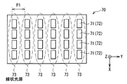
複数の光源61のうち光源61aを除く複数の光源61(以下、「光源61b」と称する。)は、表示装置において二次元表示を行うときに、光源61aと共に、面状照明光の生成に用いられるものである。つまり、表示装置において二次元表示を行うときには、面状照明光を生成するために、全ての光源61が用いられる。複数の光源61aおよび複数の光源61bは、光入射面10Aと直交する方向において規則的に配列されている。例えば、図39に示したように、1つの光源61aおよび2つの光源61bを一組として、複数組の部分電極群が光入射面10Aと直交する方向に配列されている。光源61の幅は、例えば、表示装置の画素の幅よりも狭くなっている。   Among the plurality of light sources 61, a plurality of light sources 61 (hereinafter referred to as “light source 61b”) excluding the light source 61a are used for generating planar illumination light together with the light source 61a when performing two-dimensional display on the display device. It is what That is, when two-dimensional display is performed on the display device, all the light sources 61 are used to generate planar illumination light. The plurality of light sources 61a and the plurality of light sources 61b are regularly arranged in a direction orthogonal to the light incident surface 10A. For example, as shown in FIG. 39, one light source 61a and two light sources 61b are taken as a set, and a plurality of sets of partial electrode groups are arranged in a direction orthogonal to the light incident surface 10A. For example, the width of the light source 61 is narrower than the width of the pixel of the display device.

各光源61は、例えば、図40に示したように、ブロック形状となっており、かつ複数の光源61が2次元配置されていてもよい。この場合には、複数の光源61を1つの線状光源62とみなしたときに、各線状光源62が上記の光源61a,61bとして用いられてもよい。例えば、複数の線状光源62のうち特定の複数の線状光源62(線状光源62a)が、光源61aとして用いられる。さらに、例えば、複数の線状光源62のうち線状光源61aとして用いられるものを除く複数の線状光源62(線状光源62b)が、光源61bとして用いられる。   For example, as shown in FIG. 40, each light source 61 has a block shape, and a plurality of light sources 61 may be two-dimensionally arranged. In this case, when the plurality of light sources 61 are regarded as one linear light source 62, each linear light source 62 may be used as the light sources 61a and 61b. For example, a specific plurality of linear light sources 62 (linear light sources 62a) among the plurality of linear light sources 62 are used as the light source 61a. Further, for example, a plurality of linear light sources 62 (linear light sources 62b) excluding those used as the linear light sources 61a among the plurality of linear light sources 62 are used as the light sources 61b.

なお、各光源61がブロック形状となっており、かつ複数の光源61が2次元配置されている場合に、表示装置において三次元表示を行うときに、個々の光源61が点状照明光の生成に用いられてもよい。また、各光源61がブロック形状となっており、かつ複数の光源61が2次元配置されている場合に、表示装置において2視点から互いに異なる二次元映像を視認可能な二次元表示を行うときにも、個々の光源61が点状照明光の生成に用いられてもよい。   When each light source 61 has a block shape and a plurality of light sources 61 are two-dimensionally arranged, each light source 61 generates point illumination light when performing three-dimensional display on the display device. May be used. In addition, when each light source 61 has a block shape and a plurality of light sources 61 are two-dimensionally arranged, when performing two-dimensional display in which different two-dimensional images can be viewed from two viewpoints on the display device Alternatively, the individual light sources 61 may be used for generating the point illumination light.

また、例えば、図41に示したように、各光源61が、光入射面10Aと直角以外の角度で斜めに交差する方向に延在していてもよい。また、各光源61がブロック形状となっており、かつ複数の光源61が2次元配置されている場合に、例えば、図42に示したように、各線状光源62が、光入射面10Aと直角以外の角度で斜めに交差する方向に延在していてもよい。   For example, as shown in FIG. 41, each light source 61 may extend in a direction that obliquely intersects with the light incident surface 10A at an angle other than a right angle. Further, when each light source 61 has a block shape and a plurality of light sources 61 are two-dimensionally arranged, for example, as shown in FIG. 42, each linear light source 62 is perpendicular to the light incident surface 10A. You may extend in the direction which crosses diagonally at angles other than.

本実施の形態において、反射板40は、光源60からの光を光源60側に戻すものである。反射板40は、例えば、反射、拡散、散乱などの機能を有している。これにより、光源60からの出射光を効率的に利用することができ、また、正面輝度の向上にも役立っている。反射板40の微細形状の表面は、鏡面となっていることが好ましい。この場合には、光源60からの出射光を正反射(鏡面反射)することができ、効率的に焦点Cに反射することができる。反射板40の材料は、上記の第1の実施の形態で既に述べたものと同様のものからなる。   In the present embodiment, the reflection plate 40 returns light from the light source 60 to the light source 60 side. The reflector 40 has functions such as reflection, diffusion, and scattering. Thereby, the emitted light from the light source 60 can be used efficiently, and it also helps to improve the front luminance. The finely shaped surface of the reflector 40 is preferably a mirror surface. In this case, the light emitted from the light source 60 can be regularly reflected (specular reflection), and can be efficiently reflected to the focal point C. The material of the reflector 40 is the same as that already described in the first embodiment.

反射板40は、例えば、図43に示したように、光源61から距離H1だけ離れた位置に配置されており、光源61側に反射面40Aを有している。反射面40Aは、光源60からの出射光の一部を、照明装置2の上面の方へ反射するものである。より具体的には、反射板40は、表示装置において三次元表示を行うときに、光源61aにおいて生成される線状照明光を反射することにより、焦点を結ぶ反射光を生成するものである。   For example, as shown in FIG. 43, the reflecting plate 40 is disposed at a position away from the light source 61 by a distance H1, and has a reflecting surface 40A on the light source 61 side. The reflection surface 40 </ b> A reflects a part of the light emitted from the light source 60 toward the upper surface of the lighting device 2. More specifically, the reflector 40 generates reflected light for focusing by reflecting linear illumination light generated by the light source 61a when performing three-dimensional display on the display device.

なお、反射板40は、各光源61が点状照明光を生成する場合であって、かつ表示装置において三次元表示を行うときに、各点状照明光を反射することにより、焦点を結ぶ線状の反射光を生成するものであってもよい。また、反射板40は、各光源61が点状照明光を生成する場合であって、かつ表示装置において2視点から互いに異なる二次元映像を視認可能な二次元表示を行うときに、各点状照明光を反射することにより、焦点を結ぶ線状の反射光を生成するものであってもよい。   In addition, the reflecting plate 40 is a case where each light source 61 generates point-like illumination light, and when performing three-dimensional display on the display device, the reflecting plate 40 reflects each point-like illumination light so as to connect the focal points. It is also possible to generate a reflected light having a shape. In addition, the reflector 40 is a case where each light source 61 generates point illumination light, and when performing two-dimensional display in which two-dimensional images different from each other can be viewed from two viewpoints on the display device. By reflecting the illumination light, a linear reflected light that connects the focal points may be generated.

反射板40は、線状照明光を生成する部位(光源61a)を通過する平面であって、かつ反射板40を含む平面と垂直な平面上またはその平面の近傍に反射光を反射するようになっている。より具体的には、反射板40は、線状照明光において、線状照明光を生成する部位(光源61a)と垂直な平面と平行な光の成分を考えた場合に、線状照明光を生成する部位(光源61a)を通過する線分であって、かつ反射板40を含む平面の法線と平行な線分の上またはその線分の近傍に焦点を結ぶ反射光を生成する凹凸形状を有している。さらに、反射板40は、線状照明光において、線状照明光を生成する部位(光源61a)と垂直な平面と交差する光の成分を考えた場合に、線状照明光からの光を、線状照明光を生成する部位(光源61a)またはその近傍に反射する凹凸形状を有している。ここで、反射面40Aが、生成された光を、その光が生成された方へ反射させるようになっている場合、これを式で表すと、例えば以下のようになる。つまり、反射板40は、2次元再帰性の反射の性質を有している。
反射前の光のベクトルV=(Vx,Vy,Vz)
反射後の光のベクトルV=(Vx,−Vy,−Vz)
The reflecting plate 40 is a plane that passes through a portion (the light source 61a) that generates linear illumination light, and reflects the reflected light on or near a plane that is perpendicular to the plane that includes the reflecting plate 40. It has become. More specifically, the reflecting plate 40, when considering the light component parallel to the plane perpendicular to the portion (the light source 61a) that generates the linear illumination light, in the linear illumination light, Concave and convex shape that generates reflected light that is focused on or near a line segment that passes through the region to be generated (light source 61a) and is parallel to the normal line of the plane including the reflector 40 have. Furthermore, when the reflector 40 considers a component of light that intersects a plane perpendicular to the portion that generates the linear illumination light (light source 61a) in the linear illumination light, the light from the linear illumination light is It has a concavo-convex shape that is reflected at or near the site (light source 61a) that generates linear illumination light. Here, when the reflection surface 40A reflects the generated light toward the direction in which the light is generated, this can be expressed by the following formula, for example. That is, the reflector 40 has a two-dimensional recursive reflection property.
Vector of light before reflection V = (Vx, Vy, Vz)
Vector of reflected light V = (Vx, −Vy, −Vz)

例えば、図43に示したように、線状照明光を生成する部位(光源61a)と垂直な平面と平行な光の成分を考えた場合に、反射板40は、線分AX3の上またはその線分AX3の近傍であって、かつ光源61aの直下に反射光が焦点Cを結ぶ凹凸形状を有している。このとき、焦点Cの位置と、反射板40の上面との距離H2は、距離H1よりも短くなっており、(H1/n1−W1)以上、H1未満となっていることが好ましい。なお、n1は、反射板40の上面と、焦点Cの位置との間の領域の屈折率であり、本実施の形態では例えば大気の屈折率である。   For example, as shown in FIG. 43, when considering a light component parallel to a plane perpendicular to a portion (light source 61a) that generates linear illumination light, the reflector 40 is on the line segment AX3 or its In the vicinity of the line segment AX3 and directly under the light source 61a, the reflected light has an uneven shape that connects the focal point C. At this time, the distance H2 between the position of the focal point C and the upper surface of the reflecting plate 40 is shorter than the distance H1, and is preferably (H1 / n1-W1) or more and less than H1. Note that n1 is the refractive index of the region between the upper surface of the reflector 40 and the position of the focal point C, and is, for example, the refractive index of the atmosphere in the present embodiment.

なお、例えば、図44に示したように、線状照明光を生成する部位(光源61a)と垂直な平面と平行な光の成分を考えた場合に、反射板40は、線分AX3の上またはその線分AX3の近傍であって、かつ光源61aの直上に反射光が焦点Cを結ぶ凹凸形状を有していてもよい。このとき、距離H2は、距離H1よりも長くなっており、H1よりも大きく、(H1/n1+W1)以下となっていることが好ましい。また、例えば、図45に示したように、線状照明光を生成する部位(光源61a)と垂直な平面と平行な光の成分を考えた場合に、反射板40は、線分AX3の上またはその線分AX3の近傍であって、かつ光源61a内に反射光が焦点Cを結ぶ凹凸形状を有していてもよい。このとき、距離H2は、距離H1と概ね等しくなる。   For example, as shown in FIG. 44, when considering a light component parallel to a plane perpendicular to a portion (light source 61a) that generates linear illumination light, the reflector 40 is above the line segment AX3. Alternatively, it may have a concavo-convex shape in which the reflected light connects the focal point C in the vicinity of the line segment AX3 and directly above the light source 61a. At this time, it is preferable that the distance H2 is longer than the distance H1, larger than H1, and not more than (H1 / n1 + W1). Further, for example, as shown in FIG. 45, when considering a light component parallel to a plane perpendicular to a portion (light source 61a) that generates linear illumination light, the reflector 40 is above the line segment AX3. Or you may have the uneven | corrugated shape which the reflected light connects the focus C in the vicinity of the line segment AX3, and in the light source 61a. At this time, the distance H2 is substantially equal to the distance H1.

反射板40は、中心軸が焦点Cを通過する円柱の内面の一部を反射面40Aとして有している。反射面40Aは、光源61aと対向する位置が最も深くなっていることが好ましい。   The reflection plate 40 has a part of the inner surface of a cylinder whose central axis passes through the focal point C as a reflection surface 40A. The reflective surface 40A is preferably deepest at the position facing the light source 61a.

焦点Cの位置は、図43、図44、図45を比較した場合、図45に記載した位置(光源61a内)となっていることが最も良い。このとき、焦点Cの位置は、H2=H1/n1を満たす位置となっていることが最も良い。反射板40の反射面40Aにおける立体形状のピッチP2は、光源61(線状照明光を生成する部位)のピッチP1と一致しているか、またはほぼ一致していることが最も良い。この場合に、さらに、反射面40Aのうち円柱の内面の一部に相当する部分の半径は、(H22+(P1/2)21/2となっていることが最も良い。このようにした場合には、反射面40Aで反射された光が、焦点Cに向かって進み、光源61に再帰的に到達する。なお、本実施の形態における反射板40によって生成される反射光の正面輝度分布および角度輝度分布は、上記第1の実施の形態における反射板40のそれらと同様である。 When comparing FIG. 43, FIG. 44, and FIG. 45, the position of the focal point C is best at the position described in FIG. 45 (within the light source 61a). At this time, it is best that the position of the focal point C is a position that satisfies H2 = H1 / n1. It is best that the three-dimensional pitch P2 on the reflecting surface 40A of the reflecting plate 40 coincides with or substantially coincides with the pitch P1 of the light source 61 (part that generates linear illumination light). In this case, the radius of the portion corresponding to a part of the inner surface of the cylinder in the reflecting surface 40A is preferably (H2 2 + (P1 / 2) 2 ) 1/2 . In this case, the light reflected by the reflecting surface 40A travels toward the focal point C and reaches the light source 61 recursively. The front luminance distribution and the angular luminance distribution of the reflected light generated by the reflecting plate 40 in the present embodiment are the same as those of the reflecting plate 40 in the first embodiment.

次に、本実施の形態の照明装置2の作用および効果について説明する。   Next, the operation and effect of the lighting device 2 of the present embodiment will be described.

本実施の形態の照明装置2では、三次元表示のときに、光源60において、各光源61aが発光し、各光源61bが消光している。各光源61aから発せられた光は直接、正面方向に出射されると共に、反射板40で反射された光が正面方向に出射される。これにより、正面方向に線状照明光が出力される。   In the illumination device 2 of the present embodiment, in the three-dimensional display, in the light source 60, each light source 61a emits light and each light source 61b is extinguished. The light emitted from each light source 61a is directly emitted in the front direction, and the light reflected by the reflecting plate 40 is emitted in the front direction. Thereby, linear illumination light is output in the front direction.

また、本実施の形態の照明装置2では、二次元表示のときに、光源60において、全ての光源61が発光している。各光源61から発せられた光は直接、正面方向に出射されると共に、反射板40で反射された光が正面方向に出射される。これにより、正面方向に面状照明光が出力される。   In the illumination device 2 of the present embodiment, all light sources 61 emit light in the light source 60 during two-dimensional display. The light emitted from each light source 61 is directly emitted in the front direction, and the light reflected by the reflecting plate 40 is emitted in the front direction. Thereby, planar illumination light is output in the front direction.

ところで、本実施の形態では、三次元表示に際して、パララックスバリアを設ける必要がない。また、仮に、パララックスバリアを、照明装置2の光出射側に設けたとしても、そのときに、複数の光源61のうちのパララックスバリアの光透過領域に対応する光源61を選択的に発光させることで、光源60から出力された光がパララックスバリアで吸収される割合を極めて低くすることができる。また、本実施の形態では、三次元表示に際して、シリンドリカルレンズを必要としないので、シリンドリカルレンズに起因する収差の問題が生じる虞はない。   By the way, in this embodiment, it is not necessary to provide a parallax barrier for three-dimensional display. Even if a parallax barrier is provided on the light emitting side of the illumination device 2, the light source 61 corresponding to the light transmission region of the parallax barrier among the plurality of light sources 61 is selectively emitted at that time. By making it, the ratio by which the light output from the light source 60 is absorbed by a parallax barrier can be made extremely low. In this embodiment, since a cylindrical lens is not required for three-dimensional display, there is no possibility that an aberration problem caused by the cylindrical lens occurs.

また、本実施の形態では、線状照明光が反射板40で反射されることにより、焦点を結ぶ反射光L12が生成される。これにより、反射光L12の正面強度分布および角度強度分布を、線状照明光のうち反射板40とは反対側に出射された光L13の正面強度分布および角度強度分布に近づけることができる。その結果、反射板の上面を平坦面で構成した場合(図22参照)や、平行光を生成する放物曲面で構成した場合(図20参照)と比べて、三次元表示の際に、反射光L13が光源61とは異なる領域を通過して上面から出射される割合を減らすことができる。さらに、反射光L13が三次元表示に必要のない角度方向に出射される割合を少なくすることもできる。これにより、このような照明装置2を三次元表示用の表示装置のバックライトとして適用した場合に、三次元表示における二重像の生成を低減することができる。従って、三次元表示における表示品質が向上する。   Further, in the present embodiment, the linear illumination light is reflected by the reflecting plate 40, thereby generating reflected light L12 for focusing. Thereby, the front intensity distribution and the angular intensity distribution of the reflected light L12 can be brought close to the front intensity distribution and the angular intensity distribution of the light L13 emitted to the side opposite to the reflecting plate 40 in the linear illumination light. As a result, compared with the case where the upper surface of the reflecting plate is configured as a flat surface (see FIG. 22) and the case where it is configured as a parabolic curved surface that generates parallel light (see FIG. 20), reflection is performed in three-dimensional display. The rate at which the light L13 is emitted from the upper surface through a different region from the light source 61 can be reduced. Furthermore, the ratio of the reflected light L13 emitted in an angular direction that is not necessary for three-dimensional display can be reduced. Thereby, when such an illuminating device 2 is applied as a backlight of a display device for three-dimensional display, generation of a double image in three-dimensional display can be reduced. Therefore, the display quality in the three-dimensional display is improved.

<4.第2の実施の形態の変形例>
上記第2の実施の形態において、光源61が点状照明光を生成するときに、反射板40は、球面の一部を反射面40Aとして有していてもよい。このとき、反射板40は、光源61と対向する位置が最も深くなっていることが好ましい。反射板40がこのような反射面40Aを有している場合であっても、この照明装置2を三次元表示用の表示装置のバックライトとして適用した場合に、三次元表示における二重像の生成を低減することができる。従って、三次元表示における表示品質が向上する。
<4. Modification of Second Embodiment>
In the second embodiment, when the light source 61 generates the point illumination light, the reflection plate 40 may have a part of the spherical surface as the reflection surface 40A. At this time, it is preferable that the reflecting plate 40 has the deepest position facing the light source 61. Even when the reflector 40 has such a reflective surface 40A, when the illumination device 2 is applied as a backlight of a display device for three-dimensional display, a double image in three-dimensional display is displayed. Production can be reduced. Therefore, the display quality in the three-dimensional display is improved.

<5.第3の実施の形態>
図46は、第3の実施の形態に係る照明装置3の断面構成を表すものである。この照明装置3は、表示装置のバックライトとして適用可能なものであり、例えば、図46に示したように、導光板70と、導光板70の側面に配置した光源20と、導光板70の背後に配置された反射板40とを備えている。なお、導光板70および光源20が、「照明光学系」の一具体例に相当する。
<5. Third Embodiment>
FIG. 46 illustrates a cross-sectional configuration of the illumination device 3 according to the third embodiment. The illumination device 3 can be applied as a backlight of a display device. For example, as shown in FIG. 46, the light guide plate 70, the light source 20 disposed on the side surface of the light guide plate 70, and the light guide plate 70 And a reflector 40 disposed behind. The light guide plate 70 and the light source 20 correspond to a specific example of “illumination optical system”.

導光板70は、導光板10の側面に配置した光源20からの光を導光板70の上面側(例えば照明装置3の光出射面3A(図46参照))に導くものである。この導光板70は、例えば、導光板70の上面に配置される被照射物(例えば後述の表示パネル210)に対応した形状になっており、例えば、上面、下面および側面で囲まれた直方体状となっている。なお、以下では、導光板70の側面のうち光源20からの光が入射する側面を光入射面70Aと称するものとする。   The light guide plate 70 guides light from the light source 20 disposed on the side surface of the light guide plate 10 to the upper surface side of the light guide plate 70 (for example, the light emission surface 3A of the illumination device 3 (see FIG. 46)). For example, the light guide plate 70 has a shape corresponding to an object to be irradiated (for example, a display panel 210 described later) disposed on the upper surface of the light guide plate 70. It has become. Hereinafter, the side surface on which light from the light source 20 enters among the side surfaces of the light guide plate 70 is referred to as a light incident surface 70A.

導光板70は、例えば、導光板70内を伝播する光を散乱させる散乱部を有している。散乱部は、例えば、フィラーを含んだ部位であったり、散乱材が印刷されたものであったり、微細な突起(凸部)であったりする。以下では、導光板70が、散乱部として、微細な突起である凸部71を複数、上面に有しているものとして本実施の形態を説明する。なお、以下の説明において、凸部71を散乱部と読み替えることが可能である。   The light guide plate 70 has, for example, a scattering portion that scatters light propagating through the light guide plate 70. The scattering portion is, for example, a part including a filler, a material on which a scattering material is printed, or a fine protrusion (convex portion). Hereinafter, the present embodiment will be described on the assumption that the light guide plate 70 has a plurality of convex portions 71, which are fine protrusions, on the upper surface as scattering portions. In the following description, the convex portion 71 can be read as a scattering portion.

複数の凸部71は、例えば、図47に示したように、面内の一の方向(例えば光入射面70Aに平行な方向)に延在する帯状の形状となっている。各凸部71は、表示装置において三次元表示を行うときに、線状照明光の生成に用いられるものである。複数の凸部71は、表示装置において三次元表示を行うときの画素のピッチP3(図61参照)に対応するピッチP1(画素のピッチP3と同一ピッチまたはそれに近いピッチ)で配列されている。   For example, as shown in FIG. 47, the plurality of convex portions 71 have a band-like shape extending in one direction in the plane (for example, a direction parallel to the light incident surface 70A). Each convex portion 71 is used to generate linear illumination light when performing three-dimensional display on the display device. The plurality of convex portions 71 are arranged at a pitch P1 (the same pitch as the pixel pitch P3 or a pitch close thereto) corresponding to the pixel pitch P3 (see FIG. 61) when performing three-dimensional display in the display device.

各凸部71は、導光板70内を伝播する光を散乱させる材料(例えばフィラー)または構造(例えば光散乱面)を含んでいる。そのため、各凸部71の全体または一部が散乱領域72となっている。例えば、図47に示したように、導光板70の面内において、各凸部71の全体が散乱領域72となっている。このとき、各散乱領域72は、帯状の形状となっている。なお、図示しないが、導光板70の面内において、各凸部71の一部が散乱領域72となっていてもよい。このとき、各散乱領域72がブロック形状となっており、かつ複数の散乱領域72が導光板70の面内において2次元配置されていてもよい。各凸部71は、例えば、図48に示したように、ブロック形状となっており、かつ複数の凸部71が2次元配置されていてもよい。この場合には、複数の凸部71を1つの線状凸部73とみなしたときに、各線状凸部73が、図47の凸部71として用いられてもよい。複数の凸部73は、表示装置において三次元表示を行うときの画素のピッチP3(図61参照)に対応するピッチP1(画素のピッチP3と同一ピッチまたはそれに近いピッチ)で配列されている。   Each convex portion 71 includes a material (for example, a filler) or a structure (for example, a light scattering surface) that scatters light propagating through the light guide plate 70. Therefore, the whole or part of each convex portion 71 is a scattering region 72. For example, as shown in FIG. 47, the entire convex portion 71 is a scattering region 72 in the plane of the light guide plate 70. At this time, each scattering region 72 has a strip shape. Although not shown, a part of each convex portion 71 may be a scattering region 72 in the plane of the light guide plate 70. At this time, each scattering region 72 may have a block shape, and the plurality of scattering regions 72 may be two-dimensionally arranged in the plane of the light guide plate 70. For example, as shown in FIG. 48, each convex portion 71 has a block shape, and a plurality of convex portions 71 may be two-dimensionally arranged. In this case, when the plurality of convex portions 71 are regarded as one linear convex portion 73, each linear convex portion 73 may be used as the convex portion 71 in FIG. The plurality of convex portions 73 are arranged at a pitch P1 (the same pitch as the pixel pitch P3 or a pitch close thereto) corresponding to the pixel pitch P3 (see FIG. 61) when performing three-dimensional display in the display device.

本実施の形態において、反射板40は、光源20からの光を導光板70側に戻すものである。反射板40は、例えば、反射、拡散、散乱などの機能を有している。これにより、光源20からの出射光を効率的に利用することができ、また、正面輝度の向上にも役立っている。反射板40の微細形状の表面は、鏡面となっていることが好ましい。この場合には、光源20からの出射光を正反射(鏡面反射)することができ、効率的に焦点C(後述)に反射することができる。反射板40の材料は、上記の第1の実施の形態で既に述べたものと同様のものからなる。   In the present embodiment, the reflector 40 returns the light from the light source 20 to the light guide plate 70 side. The reflector 40 has functions such as reflection, diffusion, and scattering. Thereby, the emitted light from the light source 20 can be used efficiently, and it is also useful for improving the front luminance. The finely shaped surface of the reflector 40 is preferably a mirror surface. In this case, the light emitted from the light source 20 can be regularly reflected (specular reflection), and can be efficiently reflected to the focal point C (described later). The material of the reflector 40 is the same as that already described in the first embodiment.

反射板40は、例えば、図49に示したように、散乱領域72から距離H1だけ離れた位置に配置されており、導光板70側に反射面40Aを有している。反射面40Aは、光源20からの出射光の一部を、照明装置3の上面の方(具体的には光出射面3A)へ反射するものである。   For example, as shown in FIG. 49, the reflecting plate 40 is disposed at a position away from the scattering region 72 by a distance H1, and has a reflecting surface 40A on the light guide plate 70 side. The reflection surface 40A reflects a part of the light emitted from the light source 20 toward the upper surface of the illumination device 3 (specifically, the light emission surface 3A).

なお、反射板40は、各散乱領域72が点状照明光を生成する場合であって、かつ表示装置において三次元表示を行うときに、各点状照明光を反射することにより、焦点を結ぶ線状の反射光を生成するものであってもよい。また、反射板40は、各散乱領域72が点状照明光を生成する場合であって、かつ表示装置において2視点から互いに異なる二次元映像を視認可能な二次元表示を行うときに、各点状照明光を反射することにより、焦点を結ぶ線状の反射光を生成するものであってもよい。   In addition, the reflector 40 is a case where each scattering area | region 72 produces | generates point-like illumination light, and when performing a three-dimensional display in a display apparatus, it focuses each other by reflecting each point-like illumination light. It may generate linear reflected light. In addition, the reflecting plate 40 is a case where each scattering region 72 generates point illumination light, and when performing two-dimensional display in which two-dimensional images different from each other can be viewed from two viewpoints on the display device, The linear reflected light that connects the focal points may be generated by reflecting the shaped illumination light.

反射板40は、線状照明光を生成する部位(散乱領域72)を通過する線分であって、かつ反射板40を含む平面と垂直な平面上またはその平面の近傍に反射光を反射するようになっている。より具体的には、反射板40は、線状照明光において、線状照明光を生成する部位(散乱領域72)と垂直な平面と平行な光の成分を考えた場合に、線状照明光を生成する部位(散乱領域72)を通過する線分であって、かつ反射板40を含む平面の法線と平行な線分の上またはその線分の近傍に焦点を結ぶ反射光を生成する凹凸面を有している。さらに、反射板40は、線状照明光において、線状照明光を生成する部位(光源61散乱領域72)と垂直な平面と交差する光の成分を考えた場合に、線状照明光からの光を、線状照明光を生成する部位(散乱領域72)またはその近傍に反射する凹凸面を有している。ここで、反射面40Aが、生成された光を、その光が生成された方へ反射させるようになっている場合、これを式で表すと、例えば以下のようになる。つまり、反射板40は、2次元再帰性の反射の性質を有している。
反射前の光のベクトルV=(Vx,Vy,Vz)
反射後の光のベクトルV=(Vx,−Vy,−Vz)
The reflecting plate 40 is a line segment that passes through a site (scattering region 72) that generates linear illumination light, and reflects the reflected light on or near a plane that is perpendicular to the plane that includes the reflecting plate 40. It is like that. More specifically, the reflecting plate 40 is configured so that, in the linear illumination light, when the light component parallel to the plane perpendicular to the portion (scattering region 72) that generates the linear illumination light is considered, Is generated on the line segment that passes through the region (scattering region 72) that generates the light and is parallel to the normal line of the plane including the reflector 40, or the reflected light that focuses on the line segment. Has an uneven surface. Further, the reflection plate 40 has a light component that is obtained from the linear illumination light when considering a component of the light that intersects the plane perpendicular to the portion (the light source 61 scattering region 72) that generates the linear illumination light. It has an uneven surface that reflects light at a site (scattering region 72) that generates linear illumination light or in the vicinity thereof. Here, when the reflection surface 40A reflects the generated light toward the direction in which the light is generated, this can be expressed by the following formula, for example. That is, the reflector 40 has a two-dimensional recursive reflection property.
Vector of light before reflection V = (Vx, Vy, Vz)
Vector of reflected light V = (Vx, −Vy, −Vz)

反射板40は、線状照明光を生成する部位(散乱領域72)を通過する線分であって、かつ反射板40を含む平面の法線と平行な線分AX3の上またはその線分AX3の近傍に反射光が焦点を結ぶ凹凸形状を有している。つまり、反射板40は、再帰的な反射の性質を有している。例えば、図49に示したように、反射板40は、線分AX3の上またはその線分AX3の近傍であって、かつ散乱領域72の直下に反射光が焦点Cを結ぶ凹凸形状を有している。このとき、焦点Cの位置と、反射板40の上面との距離H2は、距離H1よりも短くなっており、(H1/n1−W1)以上、H1未満となっていることが好ましい。なお、n1は、反射板40の上面と、焦点Cの位置との間の領域の屈折率であり、本実施の形態では導光板70の屈折率である。   The reflector 40 is a line segment that passes through a portion (scattering region 72) that generates linear illumination light, and is on or on the line segment AX3 parallel to the normal line of the plane including the reflector 40. , Has an uneven shape in which the reflected light is focused. That is, the reflector 40 has a recursive reflection property. For example, as shown in FIG. 49, the reflecting plate 40 has a concavo-convex shape in which the reflected light connects the focal point C on or near the line segment AX3 and directly below the scattering region 72. ing. At this time, the distance H2 between the position of the focal point C and the upper surface of the reflecting plate 40 is shorter than the distance H1, and is preferably (H1 / n1-W1) or more and less than H1. Note that n1 is the refractive index of the region between the upper surface of the reflector 40 and the position of the focal point C, and is the refractive index of the light guide plate 70 in the present embodiment.

なお、例えば、図50に示したように、線状照明光を生成する部位(散乱領域72)と垂直な平面と平行な光の成分を考えた場合に、反射板40は、線分AX3の上またはその線分AX3の近傍であって、かつ散乱領域72の直上に反射光が焦点Cを結ぶ凹凸形状を有していてもよい。このとき、距離H2は、距離H1よりも長くなっており、H1よりも大きく、(H1/n1+W1)以下となっていることが好ましい。また、例えば、図51に示したように、線状照明光を生成する部位(散乱領域72)と垂直な平面と平行な光の成分を考えた場合に、反射板40は、線分AX3の上またはその線分AX3の近傍であって、かつ散乱領域72内に反射光が焦点Cを結ぶ表面形状を有していてもよい。このとき、距離H2は、距離H1と概ね等しくなる。   For example, as shown in FIG. 50, when considering a light component parallel to a plane perpendicular to a portion (scattering region 72) that generates linear illumination light, the reflector 40 has a line segment AX3. It may have an uneven shape in which the reflected light connects the focal point C directly above or near the line segment AX3 and directly above the scattering region 72. At this time, it is preferable that the distance H2 is longer than the distance H1, larger than H1, and not more than (H1 / n1 + W1). Further, for example, as shown in FIG. 51, when considering a light component parallel to a plane perpendicular to a portion (scattering region 72) that generates linear illumination light, the reflector 40 has a line segment AX3. It may have a surface shape on the top or in the vicinity of the line segment AX3 and in which the reflected light connects the focal point C in the scattering region 72. At this time, the distance H2 is substantially equal to the distance H1.

反射板40は、中心軸が焦点Cを通過する円柱の内面の一部を反射面40Aとして有している。反射板40は、散乱領域72と対向する位置が最も深くなっていることが好ましい。   The reflection plate 40 has a part of the inner surface of a cylinder whose central axis passes through the focal point C as a reflection surface 40A. It is preferable that the position of the reflecting plate 40 facing the scattering region 72 is deepest.

焦点Cの位置は、図49、図50,図51を比較した場合、図49に記載した位置(散乱領域72の直下)となっていることが最も良い。このとき、焦点Cの位置は、H2=H1/n1を満たす位置となっていることが最も良い。反射板40の反射面40Aにおける立体形状のピッチP2は、導光板70内の散乱領域72のピッチP1と等しいか、またはほぼ等しくなっていることが最も良い。この場合に、さらに、反射面40Aのうち円柱の内面の一部に相当する部分の半径は、(H22+(P1/2)21/2となっていることが最も良い。このようにした場合には、反射面40Aで反射された光が、焦点Cに向かって進み、導光板70の底面で屈折され、散乱領域72に再帰的に到達する。 When comparing FIG. 49, FIG. 50, and FIG. 51, the position of the focal point C is best at the position described in FIG. 49 (directly below the scattering region 72). At this time, it is best that the position of the focal point C is a position that satisfies H2 = H1 / n1. The three-dimensional pitch P2 on the reflecting surface 40A of the reflecting plate 40 is best equal to or substantially equal to the pitch P1 of the scattering regions 72 in the light guide plate 70. In this case, the radius of the portion corresponding to a part of the inner surface of the cylinder in the reflecting surface 40A is preferably (H2 2 + (P1 / 2) 2 ) 1/2 . In this case, the light reflected by the reflecting surface 40A travels toward the focal point C, is refracted at the bottom surface of the light guide plate 70, and reaches the scattering region 72 recursively.

なお、各凸部71は、例えば、図52、図53、図54に示したように、導光板70の下面に形成されていてもよい。このようにした場合には、焦点Cの位置は、図54に記載した位置(散乱領域72内)となっていることが最も良い。焦点Cの位置が図54に記載した位置となっている場合には、反射板40で反射された光が、導光板70の底面で屈折されることなく、直接、散乱領域72に入射するので、照明装置3の設計が容易となる。   In addition, each convex part 71 may be formed in the lower surface of the light-guide plate 70, as shown, for example in FIG.52, FIG.53, FIG.54. In such a case, it is best that the position of the focal point C is the position shown in FIG. 54 (in the scattering region 72). When the position of the focal point C is the position described in FIG. 54, the light reflected by the reflecting plate 40 is directly refracted by the bottom surface of the light guide plate 70 and directly enters the scattering region 72. The lighting device 3 can be easily designed.

なお、本実施の形態において、反射板40は導光板70と接着されていてもよい。反射板40と導光板70との接着には、全面接着、外周部分の接着(表示領域以外の部分を環状に接着)、または点状接着(表示領域以外の部分を点状に接着)が考えられる。反射板40と導光板70とを全面接着する場合には、反射板40の頂点部分を導光板70に接着することが考えられる。このとき、反射板40の頂点部分が、若干の平坦面となっていてもよい。   In the present embodiment, the reflection plate 40 may be bonded to the light guide plate 70. Adhesion between the reflection plate 40 and the light guide plate 70 may be whole surface adhesion, adhesion of the outer peripheral portion (a portion other than the display region is adhered in a ring shape), or point-like adhesion (a portion other than the display region is adhered in a dot shape). It is done. When the entire surface of the reflection plate 40 and the light guide plate 70 is bonded, it is conceivable that the apex portion of the reflection plate 40 is bonded to the light guide plate 70. At this time, the apex portion of the reflecting plate 40 may be a slightly flat surface.

また、本実施の形態において、反射板40は、例えば、図示しないが、導光板70と接する部位に、図24に示したようなブラック43を有していてもよい。このブラック43は、例えば、反射板40を導光板70の裏面に固定する接着剤に黒色の顔料を混ぜたものであってもよい。   In the present embodiment, the reflector 40 may have a black 43 as shown in FIG. 24 at a portion in contact with the light guide plate 70, although not shown. The black 43 may be, for example, a mixture of a black pigment and an adhesive that fixes the reflecting plate 40 to the back surface of the light guide plate 70.

本実施の形態では、導光板70の各凸部71に設けられた散乱領域72から線状照明光が出力される。このとき、本実施の形態では、線状照明光が反射板40で反射されることにより、焦点を結ぶ反射光L12が生成される。これにより、反射光L12の正面強度分布および角度強度分布を、線状照明光のうち反射板40とは反対側に出射された光L13の正面強度分布および角度強度分布に近づけることができる。その結果、反射板の上面を平坦面で構成した場合(図22参照)や、平行光を生成する放物曲面で構成した場合(図20参照)と比べて、三次元表示の際に、反射光L13が散乱領域72とは異なる領域を通過して上面から出射される割合を減らすことができる。これにより、このような照明装置3を三次元表示用の表示装置のバックライトとして適用した場合に、三次元表示における二重像の生成を低減することができる。従って、三次元表示における表示品質が向上する。   In the present embodiment, linear illumination light is output from the scattering region 72 provided on each convex portion 71 of the light guide plate 70. At this time, in the present embodiment, the linear illumination light is reflected by the reflecting plate 40, thereby generating the reflected light L12 for focusing. Thereby, the front intensity distribution and the angular intensity distribution of the reflected light L12 can be brought close to the front intensity distribution and the angular intensity distribution of the light L13 emitted to the side opposite to the reflecting plate 40 in the linear illumination light. As a result, compared with the case where the upper surface of the reflecting plate is configured as a flat surface (see FIG. 22) and the case where it is configured as a parabolic curved surface that generates parallel light (see FIG. 20), reflection is performed in three-dimensional display. The rate at which the light L13 is emitted from the upper surface through a region different from the scattering region 72 can be reduced. Thereby, when such an illuminating device 3 is applied as a backlight of a display device for three-dimensional display, generation of a double image in three-dimensional display can be reduced. Therefore, the display quality in the three-dimensional display is improved.

<6.第3の実施の形態の変形例>
また、上記第3の実施の形態において、各凸部71の一部が散乱領域72となっているときに、反射板40は、球面の一部を反射面40Aとして有していてもよい。このとき、反射板40は、散乱領域72と対向する位置が最も深くなっていることが好ましい。反射板40がこのような反射面40Aを有している場合であっても、この照明装置3を三次元表示用の表示装置のバックライトとして適用した場合に、三次元表示における二重像の生成を低減することができる。従って、三次元表示における表示品質が向上する。
<6. Modification of Third Embodiment>
Moreover, in the said 3rd Embodiment, when a part of each convex part 71 is the scattering area | region 72, the reflecting plate 40 may have a part of spherical surface as the reflective surface 40A. At this time, it is preferable that the reflecting plate 40 has the deepest position facing the scattering region 72. Even when the reflector 40 has such a reflective surface 40A, when the illumination device 3 is applied as a backlight of a display device for three-dimensional display, a double image in three-dimensional display is displayed. Production can be reduced. Therefore, the display quality in the three-dimensional display is improved.

<7.上記各実施の形態に共通する変形例>
[第1共通変形例]
上記各実施の形態およびそれらの変形例において、反射面40Aは、例えば、図55に示したように、フレネルレンズとなっていてもよい。このようにした場合には、反射面40Aのうち円弧側の面とは異なる面40Bを利用して、迷光となり得る領域に伝播していった光L4を、光L4が生成された方へ反射させる(再帰反射させる)ことができる。ここで、「迷光となり得る領域に伝播していった光L4」とは、散乱領域30B、光源61aまたは散乱領域72から出射された光のうち、直下の円弧面(範囲P2)を超えて隣の円弧面へ直接伝播した光のことをいう。また、反射板40を薄くすることもできる。
<7. Modification common to the above embodiments>
[First common modification]
In each of the above-described embodiments and their modifications, the reflective surface 40A may be a Fresnel lens, for example, as shown in FIG. In this case, the light L4 that has propagated to the region that can become stray light is reflected to the direction where the light L4 is generated by using the surface 40B that is different from the arc-side surface of the reflective surface 40A. (Retroreflective). Here, the “light L4 propagated to the region that can become stray light” is adjacent to the light emitted from the scattering region 30B, the light source 61a, or the scattering region 72 beyond the arc surface (range P2) immediately below. The light that has directly propagated to the arc surface. Further, the reflecting plate 40 can be made thin.

[第2共通変形例]
また、上記各実施の形態およびそれらの変形例において、反射板40は、例えば、図56に示したように、反射板40の上面を平坦化するとともに反射面40Aを埋め込む埋め込み層45を有していてもよい。ただし、この場合には、埋め込み層45と、導光板10、光変調層30、光源60または導光板70との間に、空隙(大気)が存在していることが必要である。このようにした場合には、散乱領域30B、光源61aまたは散乱領域72から出射された光L11の光路と、反射板40で反射された光L12の光路とが互いに平行となる。そのため、焦点Cの位置は、散乱領域30B内、光源61a内または散乱領域72内となっていることが最も良い。
[Second Common Modification]
Further, in each of the above-described embodiments and their modifications, the reflecting plate 40 has, for example, a buried layer 45 that flattens the upper surface of the reflecting plate 40 and embeds the reflecting surface 40A as shown in FIG. It may be. However, in this case, it is necessary that a gap (atmosphere) exists between the embedded layer 45 and the light guide plate 10, the light modulation layer 30, the light source 60, or the light guide plate 70. In this case, the optical path of the light L11 emitted from the scattering region 30B, the light source 61a, or the scattering region 72 and the optical path of the light L12 reflected by the reflecting plate 40 are parallel to each other. Therefore, the position of the focal point C is best located in the scattering region 30B, the light source 61a, or the scattering region 72.

[第3共通変形例]
また、上記各実施の形態およびそれらの変形例において、反射板40が、線状照明光を生成する部位(第1部位)から発せられた光を、線状照明光を生成する部位であって、かつ第1部位に隣接する部位(第2部位)に向けて反射するようになっていてもよい。
[Third common modification]
In each of the above-described embodiments and their modifications, the reflector 40 is a part that generates linear illumination light from light emitted from a part (first part) that generates linear illumination light. And it may reflect toward a part (second part) adjacent to the first part.

例えば、図57に示したように、反射板40は、図中で相対的に左側に位置する部位(線状照明光を生成する部位)から発せられた光を、その光が発せられた部位の右隣りの部位(線状照明光を生成する部位)に向けて反射する曲面を反射面40Aとして有している。さらに、例えば、図57に示したように、反射板40は、図中で相対的に右側に位置する部位(線状照明光を生成する部位)から発せられた光を、その光が発せられた部位の左隣りの部位(線状照明光を生成する部位)に向けて反射する曲面を反射面40Aとして有している。   For example, as shown in FIG. 57, the reflector 40 emits light emitted from a portion located relatively on the left side in the drawing (a portion that generates linear illumination light). The reflective surface 40A has a curved surface that is reflected toward the right adjacent portion (the portion that generates linear illumination light). Further, for example, as shown in FIG. 57, the reflector 40 emits light emitted from a portion located relatively on the right side in the drawing (a portion that generates linear illumination light). The reflective surface 40A has a curved surface that reflects toward the left side of the part (part that generates linear illumination light).

ここで、線状照明光を生成する部位と、反射板40との間に屈折率が変化する境界が無い場合には、例えば、図58に示したように、反射面40Aは、線状照明光を生成する部位に焦点Cを有している。一方、線状照明光を生成する部位と、反射板40との間に屈折率が変化する境界がある場合には、例えば、図59、図60に示したように、反射面40Aは、線状照明光を生成する部位よりも上方または下方に焦点Cを有している。特に、線状照明光を生成する部位が屈折率n1の透明基板の内部に存在する場合は、焦点Cの位置と、反射板40の上面との距離H2は、H1/n1−W1≦H2≦H1/n1+W1となっていることが好ましく、H2=H1/n1となっていることが好ましい。なお、W1は、線状照明光を生成する部位(30B、61aまたは72)の幅である。   Here, when there is no boundary where the refractive index changes between the part that generates the linear illumination light and the reflecting plate 40, for example, as shown in FIG. It has a focal point C at a site that generates light. On the other hand, when there is a boundary where the refractive index changes between the part that generates the linear illumination light and the reflecting plate 40, for example, as shown in FIG. 59 and FIG. The focal point C is located above or below the portion that generates the illumination light. In particular, when the part that generates the linear illumination light is present inside the transparent substrate having the refractive index n1, the distance H2 between the position of the focal point C and the upper surface of the reflecting plate 40 is H1 / n1-W1 ≦ H2 ≦. H1 / n1 + W1 is preferable, and H2 = H1 / n1 is preferable. In addition, W1 is the width | variety of the site | part (30B, 61a or 72) which produces | generates linear illumination light.

また、線状照明光を生成する部位と、反射板40との間に屈折率が変化する境界が無い場合には、例えば、図61に示したように、反射面40Aは、反射面40A上の任意の部位40Cと、反射面40Aと対向する、線状照明光を生成する2つの部位(30B,61aまたは72)とを直線L21,L22で結んだとき、部位40Cでの法線L23が、直線L20,L21の二等分線となるような曲面となっている。また、線状照明光を生成する部位と、反射板40との間に屈折率が変化する境界が1つある場合には、例えば、図62、図63に示したように、反射面40Aは、反射面40A上の任意の部位40Cと、反射面40Aと対向する、線状照明光を生成する2つの部位(30B,61aまたは72)の上方または下方の部位(図中の焦点C)とを直線L24,L25で結んだとき、部位40Cでの法線L23が、直線L24,L25の二等分線となるような曲面となっている。特に、線状照明光を生成する部位が屈折率n1の透明基板の内部に存在する場合は、反射面40Aは、反射面40A上の任意の部位40Cと、反射面40Aと対向する、線状照明光を生成する2つの部位(30B、61aまたは72)の下方の部位(焦点Cの位置と、反射板40の上面との距離H2は、H1/n1−W1≦H2≦H1/n1+W1となっていることが好ましく、H2=H1/n1となっていることが好ましい。)とを直線L24,L25で結んだとき、部位40Cでの法線L23が、直線L24,L25の二等分線となるような曲面となっている。また、線状照明光を生成する部位と、反射板40との間で屈折率が高、低、高の順に変化する場合には、例えば、図61に示したように、反射面40Aは、反射面40A上の任意の部位40Cと、反射面40Aと対向する、線状照明光を生成する2つの部位(30B,61aまたは72)とを直線L21,L22で結んだとき、部位40Cでの法線L23が、直線L20,L21の二等分線となるような曲面となっている。この場合は、線状照明光を生成する部位が透明基板の内部に存在し、かつ、後述するように、反射板40の上面を平坦化するとともに反射面40Cを埋め込む埋め込み層45を有している場合に相当する。   Further, when there is no boundary where the refractive index changes between the part that generates the linear illumination light and the reflecting plate 40, for example, as shown in FIG. 61, the reflecting surface 40A is on the reflecting surface 40A. 40C and the two parts (30B, 61a or 72) that generate the linear illumination light facing the reflecting surface 40A are connected by straight lines L21 and L22, the normal L23 at the part 40C is The curved surface is a bisector of the straight lines L20 and L21. Further, when there is one boundary where the refractive index changes between the part that generates the linear illumination light and the reflection plate 40, for example, as shown in FIGS. An arbitrary portion 40C on the reflecting surface 40A, and a portion (focal point C in the figure) above or below the two portions (30B, 61a, or 72) that generate the linear illumination light facing the reflecting surface 40A. Are connected by straight lines L24 and L25, the normal line L23 at the portion 40C is a curved surface that is a bisector of the straight lines L24 and L25. In particular, when a part that generates linear illumination light is present inside a transparent substrate having a refractive index n1, the reflective surface 40A is a linear shape that faces the arbitrary part 40C on the reflective surface 40A and the reflective surface 40A. The lower part of the two parts (30B, 61a or 72) that generate the illumination light (the distance H2 between the position of the focal point C and the upper surface of the reflector 40 is H1 / n1-W1≤H2≤H1 / n1 + W1). H2 = H1 / n1 is preferable.) Is connected by the straight lines L24 and L25, and the normal line L23 at the portion 40C is the bisector of the straight lines L24 and L25. It is a curved surface. Further, when the refractive index changes in the order of high, low, high between the part that generates the linear illumination light and the reflective plate 40, for example, as shown in FIG. When an arbitrary part 40C on the reflective surface 40A and two parts (30B, 61a or 72) that generate linear illumination light facing the reflective surface 40A are connected by straight lines L21 and L22, the part 40C The normal line L23 is a curved surface that is a bisector of the straight lines L20 and L21. In this case, the portion that generates the linear illumination light is present inside the transparent substrate, and has an embedded layer 45 that flattens the upper surface of the reflecting plate 40 and embeds the reflecting surface 40C as described later. It corresponds to the case.

反射板40における立体形状のピッチP2(反射面40Aの幅)は、線状照明光を生成する部位(30B,61aまたは72)のピッチP1の2倍となっている。反射面40Aは、互いに隣接する2つの部位(30B,61aまたは72)の中間領域と対向する位置が最も深い凹状の曲面となっている。   The three-dimensional pitch P2 (the width of the reflecting surface 40A) in the reflecting plate 40 is twice the pitch P1 of the portion (30B, 61a or 72) that generates the linear illumination light. The reflective surface 40A is a concave curved surface having the deepest position facing the intermediate region between two adjacent portions (30B, 61a, or 72).

本変形例では、上記各実施の形態と同様、線状照明光が反射板40で反射されることにより、焦点を結ぶ反射光が生成される。これにより、反射光の正面強度分布および角度強度分布を、線状照明光のうち反射板40とは反対側に出射された光の正面強度分布および角度強度分布に近づけることができる。その結果、反射板の上面を平坦面で構成した場合(図22参照)や、平行光を生成する放物曲面で構成した場合(図20参照)と比べて、三次元表示の際に、反射光が線状照明光を生成する部位とは異なる領域を通過して上面から出射される割合を減らすことができる。これにより、このような照明装置を三次元表示用の表示装置のバックライトとして適用した場合に、三次元表示における二重像の生成を低減することができる。従って、三次元表示における表示品質が向上する。   In the present modification, as in the above embodiments, the linear illumination light is reflected by the reflecting plate 40 to generate reflected light that focuses. Thereby, the front intensity distribution and the angle intensity distribution of the reflected light can be brought close to the front intensity distribution and the angle intensity distribution of the light emitted to the side opposite to the reflecting plate 40 in the linear illumination light. As a result, compared with the case where the upper surface of the reflecting plate is configured as a flat surface (see FIG. 22) and the case where it is configured as a parabolic curved surface that generates parallel light (see FIG. 20), reflection is performed in three-dimensional display. It is possible to reduce the ratio of light that is emitted from the upper surface through a region different from the region that generates the linear illumination light. Thereby, when such an illuminating device is applied as a backlight of a display device for three-dimensional display, generation of a double image in three-dimensional display can be reduced. Therefore, the display quality in the three-dimensional display is improved.

なお、本変形例において、反射板40が、例えば、図64に示したように、フレネルレンズとなっていてもよい。このようにした場合には、反射板40を薄くすることができる。また、本変形例において、反射板40が、図65に示したように、反射板40の上面を平坦化するとともに反射面40Cを埋め込む埋め込み層45を有していてもよい。ただし、この場合には、埋め込み層45と、導光板10、光変調層30、光源60または導光板70との間に、空隙(大気)が存在していることが必要である。このようにした場合には、散乱領域30B、光源61aまたは散乱領域72から出射された光の光路と、反射板40で反射された光の光路とが互いに平行となる。そのため、焦点Cの位置は、散乱領域30B内、光源61a内または散乱領域72内となっていることが最も良い。   In this modification, the reflector 40 may be a Fresnel lens as shown in FIG. 64, for example. In such a case, the reflecting plate 40 can be made thin. Further, in the present modification, as shown in FIG. 65, the reflecting plate 40 may have an embedded layer 45 that flattens the upper surface of the reflecting plate 40 and embeds the reflecting surface 40C. However, in this case, it is necessary that a gap (atmosphere) exists between the embedded layer 45 and the light guide plate 10, the light modulation layer 30, the light source 60, or the light guide plate 70. In this case, the optical path of the light emitted from the scattering region 30B, the light source 61a or the scattering region 72 and the optical path of the light reflected by the reflecting plate 40 are parallel to each other. Therefore, the position of the focal point C is best located in the scattering region 30B, the light source 61a, or the scattering region 72.

<8.第4の実施の形態>
次に、上記各実施の形態およびそれらの変形例に係る照明装置1,2,3を備えた、テレビ放送信号の受送信システムについて説明する。
<8. Fourth Embodiment>
Next, a television broadcast signal transmission / reception system provided with illumination devices 1, 2, and 3 according to the above-described embodiments and modifications thereof will be described.

図66は、第4の実施の形態に係る、テレビ放送信号100Aの受送信システムの構成例を示すブロック図である。この受送信システムは、例えば、有線(ケーブルTVなど)や無線(地上デジタル波、衛星波など)を介してテレビ放送信号を送信する送信側装置100と、上記の有線や無線を介して送信側装置100からのテレビ放送信号を受信する受信側装置200とを備えている。なお、受信側装置200が「表示装置」の一具体例に相当する。   FIG. 66 is a block diagram illustrating a configuration example of a system for receiving and transmitting a television broadcast signal 100A according to the fourth embodiment. The transmission / reception system includes, for example, a transmission-side device 100 that transmits a television broadcast signal via wired (cable TV or the like) or wireless (terrestrial digital wave, satellite wave, or the like), and the transmission side via the wired or wireless transmission described above. And a receiving-side device 200 that receives a television broadcast signal from the device 100. The reception-side device 200 corresponds to a specific example of “display device”.

テレビ放送信号100Aは、二次元表示(平面表示)用の映像データ、または三次元表示(立体表示)用の映像データを含んでいる。ここで、二次元表示用の映像データとは、視点情報を持たない二次元映像データを指している。また、三次元表示用の映像データとは、視点情報を持った二次元映像データを指しており、三次元表示用の映像データは、視点が互いに異なる複数の二次元映像データを含んで構成されている。送信側装置100は、例えば、放送局に設置されたテレビ放送信号送信装置、またはインターネット上のサーバなどである。   The television broadcast signal 100A includes video data for two-dimensional display (planar display) or video data for three-dimensional display (stereoscopic display). Here, the video data for 2D display refers to 2D video data having no viewpoint information. The video data for 3D display refers to 2D video data having viewpoint information, and the video data for 3D display includes a plurality of 2D video data having different viewpoints. ing. The transmission-side device 100 is, for example, a television broadcast signal transmission device installed in a broadcasting station or a server on the Internet.

[受信側装置200の機能ブロック]
図67は、受信側装置200の構成例を示すブロック図である。受信側装置200は、例えば、上記の有線や無線に接続可能なテレビジョンである。受信側装置200は、例えば、アンテナ端子201、デジタルチューナ202、デマルチプレクサ203、演算回路204、およびメモリ205を有している。受信側装置200は、また、例えば、デコーダ206、映像信号処理回路207、グラフィック生成回路208、パネル駆動回路209、表示パネル210、バックライト211、音声信号処理回路212、音声増幅回路213、およびスピーカ214を有している。受信側装置200は、さらに、例えば、リモコン受信回路215、およびリモコン送信機216を有している。
[Functional Block of Receiving Device 200]
FIG. 67 is a block diagram illustrating a configuration example of the reception-side apparatus 200. The reception-side device 200 is, for example, a television that can be connected to the above-described wired or wireless connection. The reception-side device 200 includes, for example, an antenna terminal 201, a digital tuner 202, a demultiplexer 203, an arithmetic circuit 204, and a memory 205. The reception-side device 200 also includes, for example, a decoder 206, a video signal processing circuit 207, a graphic generation circuit 208, a panel drive circuit 209, a display panel 210, a backlight 211, an audio signal processing circuit 212, an audio amplification circuit 213, and a speaker. 214. The reception-side device 200 further includes, for example, a remote control reception circuit 215 and a remote control transmitter 216.

なお、バックライト211が、上記各実施の形態およびそれらの変形例に係る照明装置1,2,3に相当する。また、表示パネル210が「表示パネル」の一具体例に相当し、バックライト211が「照明装置」の一具体例に相当する。   The backlight 211 corresponds to the illuminating devices 1, 2, and 3 according to the above-described embodiments and their modifications. The display panel 210 corresponds to a specific example of “display panel”, and the backlight 211 corresponds to a specific example of “illumination device”.

アンテナ端子201は、受信アンテナ(図示せず)で受信されたテレビ放送信号を入力する端子である。デジタルチューナ202は、例えば、アンテナ端子201に入力されたテレビ放送信号を処理して、ユーザの選択チャネルに対応した所定のトランスポートストリームを出力するようになっている。デマルチプレクサ203は、例えば、デジタルチューナ202で得られたトランスポートストリームから、ユーザの選択チャネルに対応したパーシャルTS(Transport Stream)を抽出するようになっている。   The antenna terminal 201 is a terminal for inputting a television broadcast signal received by a receiving antenna (not shown). For example, the digital tuner 202 processes a television broadcast signal input to the antenna terminal 201 and outputs a predetermined transport stream corresponding to the user's selected channel. For example, the demultiplexer 203 extracts a partial TS (Transport Stream) corresponding to the user's selected channel from the transport stream obtained by the digital tuner 202.

演算回路204は、受信側装置200の各部の動作を制御するものである。演算回路204は、例えば、デマルチプレクサ203で得られたパーシャルTSをメモリ205内に格納したり、メモリ205から読み出したパーシャルTSをデコーダ206に送信したりするようになっている。また、演算回路204は、例えば、二次元表示または三次元表示を指定する制御信号204Aを映像信号処理回路207およびバックライト211に送信するようになっている。演算回路204は、上記の制御信号204Aを、例えば、メモリ205内に格納された設定情報、パーシャルTSに含まれる所定の情報、またはリモコン受信回路215から入力された設定情報に基づいて設定するようになっている。   The arithmetic circuit 204 controls the operation of each unit of the receiving side device 200. The arithmetic circuit 204 stores, for example, the partial TS obtained by the demultiplexer 203 in the memory 205 and transmits the partial TS read from the memory 205 to the decoder 206. Further, the arithmetic circuit 204 is configured to transmit a control signal 204A for designating, for example, two-dimensional display or three-dimensional display to the video signal processing circuit 207 and the backlight 211. The arithmetic circuit 204 sets the control signal 204A based on, for example, setting information stored in the memory 205, predetermined information included in the partial TS, or setting information input from the remote control receiving circuit 215. It has become.

メモリ205は、例えば、受信側装置200の設定情報の格納およびデータ管理を行うものである。メモリ205は、例えば、デマルチプレクサ203で得られたパーシャルTSや、表示方法などの設定情報を格納することが可能となっている。   The memory 205 stores, for example, setting information and data management of the receiving-side apparatus 200. The memory 205 can store, for example, setting information such as a partial TS obtained by the demultiplexer 203 and a display method.

デコーダ206は、例えば、デマルチプレクサ203で得られたパーシャルTSに含まれる映像PES(Packetized Elementary Stream)パケットに対してデコード処理を行うことにより映像データを得るようになっている。デコーダ206は、また、例えば、デマルチプレクサ203で得られたパーシャルTSに含まれる音声PESパケットに対してデコード処理を行うことにより音声データを得るようになっている。ここで、映像データとは、二次元表示用の映像データ、または三次元表示用の映像データを指している。   The decoder 206 obtains video data by performing a decoding process on a video PES (Packetized Elementary Stream) packet included in the partial TS obtained by the demultiplexer 203, for example. The decoder 206 also obtains audio data by performing decoding processing on an audio PES packet included in the partial TS obtained by the demultiplexer 203, for example. Here, the video data refers to video data for 2D display or video data for 3D display.

映像信号処理回路207およびグラフィック生成回路208は、例えば、デコーダ206で得られた映像データに対して、必要に応じてマルチ画像処理、グラフィックスデータの重畳処理等を行うようになっている。   For example, the video signal processing circuit 207 and the graphic generation circuit 208 perform multi-image processing, graphics data superimposition processing, and the like on the video data obtained by the decoder 206 as necessary.

映像信号処理回路207は、演算回路204から制御信号204Aとして三次元表示を指定する信号が入力された場合であって、かつ、デコーダ206から入力された映像データが三次元表示用の映像データであったときには、例えば、デコーダ206から入力された三次元表示用の映像データに含まれる、視点の互いに異なる複数の二次元映像データを用いて1つの二次元映像データを作成し、作成した二次元映像データを、グラフィック生成回路208に出力する映像データとして選択するようになっている。例えば、三次元表示用の映像データに、視点の互いに異なる2つの二次元映像データが含まれている場合には、映像信号処理回路207は、2つの二次元映像データを、水平方向に1つずつ交互に並べる処理を各行で行っていき、2つの二次元映像データが水平方向に交互に並んだ1つの映像データを作成するようになっている。同様に、例えば、三次元表示用の映像データに、視点の互いに異なる4つの二次元映像データが含まれている場合には、映像信号処理回路207は、4つの二次元映像データを、水平方向に1つずつ周期的に並べる処理を各行で行っていき、4つの二次元映像データが水平方向に1つずつ周期的に並んだ1つの映像データを作成するようになっている。   The video signal processing circuit 207 is a case where a signal designating 3D display is input as the control signal 204A from the arithmetic circuit 204, and the video data input from the decoder 206 is video data for 3D display. If there is, for example, one 2D video data is created using a plurality of 2D video data with different viewpoints included in the video data for 3D display input from the decoder 206, and the created 2D The video data is selected as video data to be output to the graphic generation circuit 208. For example, when the video data for 3D display includes two 2D video data with different viewpoints, the video signal processing circuit 207 converts the two 2D video data into one in the horizontal direction. The processing of alternately arranging each row is performed in each row, and one video data in which two two-dimensional video data are alternately arranged in the horizontal direction is created. Similarly, for example, when the video data for 3D display includes four 2D video data with different viewpoints, the video signal processing circuit 207 converts the four 2D video data into the horizontal direction. The process of periodically arranging them one by one is performed in each row, and one video data in which four two-dimensional video data are periodically arranged one by one in the horizontal direction is created.

映像信号処理回路207は、演算回路204から制御信号204Aとして二次元表示を指定する信号が入力された場合であって、かつ、デコーダ206から入力された映像データが三次元表示用の映像データであったときには、例えば、デコーダ206から入力された三次元表示用の映像データに含まれる、視点の互いに異なる複数の二次元映像データのいずれか1つの映像データを、グラフィック生成回路208に出力する映像データとして選択するようになっている。映像信号処理回路207は、演算回路204から制御信号204Aとして二次元表示を指定する信号が入力された場合であって、かつ、デコーダ206から入力された映像データが二次元表示用の映像データであったときには、例えば、デコーダ206から入力された二次元表示用の映像データを、グラフィック生成回路208に出力する映像データとして選択するようになっている。   The video signal processing circuit 207 is a case where a signal designating two-dimensional display is input as the control signal 204A from the arithmetic circuit 204, and the video data input from the decoder 206 is video data for three-dimensional display. If there is, for example, a video that outputs any one of a plurality of 2D video data with different viewpoints included in the video data for 3D display input from the decoder 206 to the graphic generation circuit 208 Select as data. The video signal processing circuit 207 is a case where a signal designating two-dimensional display is input as the control signal 204A from the arithmetic circuit 204, and the video data input from the decoder 206 is video data for two-dimensional display. In such a case, for example, the video data for two-dimensional display input from the decoder 206 is selected as video data to be output to the graphic generation circuit 208.

グラフィック生成回路208は、例えば、画面表示の際に使用するUI(User Interface)画面を生成するようになっている。パネル駆動回路209は、例えば、グラフィック生成回路208から出力された映像データに基づいて表示パネル210を駆動するようになっている。   For example, the graphic generation circuit 208 generates a UI (User Interface) screen used for screen display. For example, the panel drive circuit 209 drives the display panel 210 based on the video data output from the graphic generation circuit 208.

表示パネル210の構成は、後に詳述する。音声信号処理回路212は、例えば、デコーダ206で得られた音声データに対してD/A変換等の処理を行うようになっている。音声増幅回路213は、例えば、音声信号処理回路212から出力された音声信号を増幅してスピーカ214に供給するようになっている。   The configuration of the display panel 210 will be described in detail later. The audio signal processing circuit 212 performs processing such as D / A conversion on the audio data obtained by the decoder 206, for example. For example, the audio amplifier circuit 213 amplifies the audio signal output from the audio signal processing circuit 212 and supplies the amplified audio signal to the speaker 214.

リモコン受信回路215は、例えば、リモコン送信機216から送信されたリモートコントロール信号を受信し、演算回路204に供給するようになっている。演算回路204は、例えば、リモートコントロール信号に従って受信側装置200の各部を制御するようになっている。   The remote control receiving circuit 215 receives a remote control signal transmitted from the remote control transmitter 216, for example, and supplies it to the arithmetic circuit 204. The arithmetic circuit 204 is configured to control each unit of the receiving side device 200 according to, for example, a remote control signal.

[受信側装置200の断面構成]
図68は、受信側装置200における表示部の断面構成の一例を表したものである。なお、図68は、模式的に表したものであり、実際の寸法や形状と同一であるとは限らない。受信側装置200は、表示パネル210と、表示パネル210の背後に配置されたバックライト211とを備えている。
[Cross-sectional configuration of receiving apparatus 200]
FIG. 68 illustrates an example of a cross-sectional configuration of a display unit in the reception-side device 200. FIG. 68 is a schematic representation and is not necessarily the same as actual dimensions and shapes. The receiving-side device 200 includes a display panel 210 and a backlight 211 disposed behind the display panel 210.

表示パネル210は、2次元配置された複数の画素を有しており、各画素または特定の画素が駆動されることにより映像を表示するものである。表示パネル210は、例えば、映像信号に応じて各画素または特定の画素が駆動される透過型の液晶表示パネル(LCD(Liquid Crystal Display))であり、液晶層を一対の透明基板で挟み込んだ構造を有している。表示パネル210は、例えば、図示しないが、バックライト211側から順に、偏光板、透明基板、画素電極、配向膜、液晶層、配向膜、共通電極、カラーフィルタ、透明基板および偏光板を有している。なお、表示パネル210において、透明基板、画素電極、配向膜、液晶層、配向膜、共通電極、カラーフィルタおよび透明基板からなる積層体が図69の液晶パネル210Aに相当する。また、バックライト211側の偏光板が図69の偏光板210Bに相当し、バックライト211とは反対側の偏光板が図69の偏光板210Cに相当する。   The display panel 210 has a plurality of pixels arranged two-dimensionally, and displays an image by driving each pixel or a specific pixel. The display panel 210 is, for example, a transmissive liquid crystal display panel (LCD (Liquid Crystal Display)) in which each pixel or specific pixel is driven according to a video signal, and has a structure in which a liquid crystal layer is sandwiched between a pair of transparent substrates. have. The display panel 210 includes, for example, a polarizing plate, a transparent substrate, a pixel electrode, an alignment film, a liquid crystal layer, an alignment film, a common electrode, a color filter, a transparent substrate, and a polarizing plate in order from the backlight 211 side, although not shown. ing. Note that in the display panel 210, a stacked body including a transparent substrate, a pixel electrode, an alignment film, a liquid crystal layer, an alignment film, a common electrode, a color filter, and a transparent substrate corresponds to the liquid crystal panel 210A in FIG. The polarizing plate on the backlight 211 side corresponds to the polarizing plate 210B in FIG. 69, and the polarizing plate on the side opposite to the backlight 211 corresponds to the polarizing plate 210C in FIG.

透明基板は、可視光に対して透明な基板、例えば板ガラスからなる。なお、バックライト211側の透明基板には、図示しないが、画素電極に電気的に接続されたTFT(Thin Film Transistor;薄膜トランジスタ)および配線などを含むアクティブ型の駆動回路が形成されている。画素電極および共通電極は、例えば、酸化インジウムスズ(ITO;Indium Tin Oxide)からなる。画素電極は、透明基板上に2次元配列されたものであり、画素ごとの電極として機能する。他方、共通電極は、カラーフィルタ上に一面に形成されたものであり、各画素電極に対して対向する共通電極として機能する。配向膜は、例えばポリイミドなどの高分子材料からなり、液晶に対して配向処理を行う。   The transparent substrate is made of a substrate transparent to visible light, for example, a plate glass. Note that an active driving circuit including a TFT (Thin Film Transistor) electrically connected to the pixel electrode and a wiring is formed on the transparent substrate on the backlight 211 side, although not shown. The pixel electrode and the common electrode are made of, for example, indium tin oxide (ITO). The pixel electrodes are two-dimensionally arranged on the transparent substrate and function as electrodes for each pixel. On the other hand, the common electrode is formed on one surface of the color filter and functions as a common electrode facing each pixel electrode. The alignment film is made of, for example, a polymer material such as polyimide, and performs alignment processing on the liquid crystal.

液晶層は、例えば、VA(Vertical Alignment)モード、TN(Twisted Nematic)モードまたはSTN(Super Twisted Nematic)モードの液晶からなり、駆動回路(図示せず)からの印加電圧により、バックライト211からの出射光の偏光軸の向きを画素ごとに変える機能を有する。なお、液晶の配列を多段階で変えることにより画素ごとの透過軸の向きが多段階で調整される。カラーフィルタは、液晶層を透過してきた光を、例えば、赤(R)、緑(G)および青(B)の三原色にそれぞれ色分離したり、または、R、G、Bおよび白(W)などの四色にそれぞれ色分離したりするカラーフィルタを、画素電極の配列と対応させて配列したものである。   The liquid crystal layer is made of, for example, VA (Vertical Alignment) mode, TN (Twisted Nematic) mode, or STN (Super Twisted Nematic) mode liquid crystal, and is applied from the backlight 211 by a voltage applied from a drive circuit (not shown). It has a function of changing the direction of the polarization axis of emitted light for each pixel. Note that the orientation of the transmission axis for each pixel is adjusted in multiple stages by changing the alignment of the liquid crystal in multiple stages. The color filter separates light transmitted through the liquid crystal layer into, for example, three primary colors of red (R), green (G), and blue (B), or R, G, B, and white (W). The color filters for separating the colors into four colors such as the above are arranged in correspondence with the arrangement of the pixel electrodes.

偏光板は、光学シャッタの一種であり、ある一定の振動方向の光(偏光)のみを通過させる。なお、偏光板は、透過軸以外の振動方向の光(偏光)を吸収する吸収型の偏光素子であってもよいが、バックライト211側に反射する反射型の偏光素子であることが輝度向上の観点から好ましい。2枚の偏光板はそれぞれ、偏光軸が互いに90°異なるように配置されており、これによりバックライト211からの出射光が液晶層を介して透過し、あるいは遮断されるようになっている。   The polarizing plate is a kind of optical shutter, and allows only light (polarized light) in a certain vibration direction to pass therethrough. The polarizing plate may be an absorptive polarizing element that absorbs light (polarized light) in a vibration direction other than the transmission axis, but it is a reflective polarizing element that reflects to the backlight 211 side to improve luminance. From the viewpoint of The two polarizing plates are arranged so that their polarization axes are different from each other by 90 °, whereby the light emitted from the backlight 211 is transmitted or blocked through the liquid crystal layer.

ところで、本実施の形態において、電圧無印加時に、バルク34Aの光軸AX1および微粒子34Bの光軸AX2が、同一の方向に光軸の成分を主に有しており、例えば、図69に示したように、配向膜33,35のラビング方向を向いていることが好ましい。さらに、電圧無印加時に、光軸AX1,AX2は、例えば、図69に示したように、バックライト211側の偏光板210Bの透過軸AX10と平行な方向に光軸の成分を主に有していることが好ましい。透過軸AX10は、例えば、図69に示したように、配向膜33,35のラビング方向を向いていることが好ましい。   By the way, in this embodiment, when no voltage is applied, the optical axis AX1 of the bulk 34A and the optical axis AX2 of the fine particles 34B mainly have the components of the optical axis in the same direction. For example, as shown in FIG. As described above, the alignment films 33 and 35 are preferably directed in the rubbing direction. Furthermore, when no voltage is applied, the optical axes AX1 and AX2, for example, mainly have an optical axis component in a direction parallel to the transmission axis AX10 of the polarizing plate 210B on the backlight 211 side, as shown in FIG. It is preferable. The transmission axis AX10 is preferably oriented in the rubbing direction of the alignment films 33 and 35, for example, as shown in FIG.

電圧無印加時には、光軸AX1,AX2は、例えば、図69に示したように、光入射面10Aの法線AX5と交差または直交(もしくはほぼ直交)する方向を向いていることが好ましい。さらに、電圧無印加時には、光軸AX1,AX2は、例えば、図2、図69に示したように、透明基板31と平行またはほぼ平行となっていることが好ましい。つまり、電圧無印加時には、光軸AX1,AX2は、概ね図69中のY軸方向を向いていることが好ましい。その理由は、上記第1の実施の形態中の[異方性散乱]の欄に記載されている。   When no voltage is applied, the optical axes AX1 and AX2 are preferably oriented in a direction intersecting or orthogonal (or substantially orthogonal) to the normal line AX5 of the light incident surface 10A as shown in FIG. 69, for example. Further, when no voltage is applied, the optical axes AX1 and AX2 are preferably parallel or substantially parallel to the transparent substrate 31 as shown in FIGS. That is, when no voltage is applied, it is preferable that the optical axes AX1 and AX2 are generally oriented in the Y-axis direction in FIG. The reason is described in the column of [Anisotropic scattering] in the first embodiment.

また、上述したように、電圧印加時には、光軸AX1は、電圧無印加時と同一またはほぼ同一の方向を向いていることが好ましい。電圧印加時には、光軸AX1は、偏光板210Bの透過軸AX10と平行な方向に光軸の成分を主に有しており、例えば、図69に示したように、透過軸AX10と平行な方向を向いていることが好ましい。電圧印加時には、光軸AX1は、光源20の光軸AX5と交差または直交(もしくはほぼ直交)する方向を向いており、さらに、透明基板31と平行またはほぼ平行となっていることが好ましい。   As described above, when a voltage is applied, the optical axis AX1 is preferably oriented in the same or substantially the same direction as when no voltage is applied. When a voltage is applied, the optical axis AX1 mainly has an optical axis component in a direction parallel to the transmission axis AX10 of the polarizing plate 210B. For example, as shown in FIG. 69, the direction parallel to the transmission axis AX10. It is preferable to face. At the time of voltage application, the optical axis AX1 is oriented in a direction intersecting or orthogonal (or substantially orthogonal) to the optical axis AX5 of the light source 20, and is preferably parallel or substantially parallel to the transparent substrate 31.

一方、光軸AX2は、電圧印加時には、下側電極32および上側電極36に印加された電圧によって生成される電場の影響を受けて所定の方向に変位していることが好ましい。電圧印加時には、光軸AX2は、例えば、図2、図69に示したように、透明基板31と交差または直交(もしくはほぼ直交)していることが好ましい。つまり、光軸AX2は、下側電極32および上側電極36への電圧印加により、光軸AX2と透明基板31の法線とのなす角度が小さくなる方向に変位していることが好ましい。このとき、光軸AX2は、光軸AX1と交差または直交(もしくはほぼ直交)しており、透明基板31と交差または直交(もしくはほぼ直交)していることが好ましい。   On the other hand, the optical axis AX2 is preferably displaced in a predetermined direction under the influence of an electric field generated by the voltage applied to the lower electrode 32 and the upper electrode 36 when a voltage is applied. When a voltage is applied, the optical axis AX2 is preferably crossed or orthogonal (or substantially orthogonal) to the transparent substrate 31, for example, as shown in FIGS. That is, it is preferable that the optical axis AX2 is displaced in a direction in which the angle formed by the optical axis AX2 and the normal line of the transparent substrate 31 is reduced by applying a voltage to the lower electrode 32 and the upper electrode 36. At this time, the optical axis AX2 preferably intersects or is orthogonal (or substantially orthogonal) with the optical axis AX1, and preferably intersects or is orthogonal (or substantially orthogonal) with the transparent substrate 31.

次に、本実施の形態の受信側装置200の作用および効果について説明する。   Next, the operation and effect of reception-side apparatus 200 of the present embodiment will be described.

本実施の形態の受信側装置200では、バックライト211として上記実施の形態およびその変形例に係る照明装置1,照明装置2または照明装置3が用いられる。これにより、三次元表示のときに、バックライト211の光射出面のうち所定の領域から、正面方向に、複数の線状照明光が出力される。これにより、正面方向に出力された各線状照明光が表示パネル210の背面に入射する。   In the reception-side device 200 of the present embodiment, the illumination device 1, the illumination device 2, or the illumination device 3 according to the above-described embodiment and its modification is used as the backlight 211. Thereby, at the time of three-dimensional display, several linear illumination light is output to a front direction from the predetermined area | region among the light emission surfaces of the backlight 211. FIG. Thereby, each linear illumination light output in the front direction enters the back surface of the display panel 210.

ここで、各線状照明光に対応する画素配列において各画素行が三次元用画素210Aとなるように三次元表示用の二次元映像データが映像信号処理回路207で生成されたときには、例えば、図70に示したように、各三次元用画素210A内の共通の位置にある画素(例えば、図70では、210−1,210−2,210−3または210−4)には、各線状照明光が略同一の角度で入射する。その結果、各三次元用画素210A内の共通の位置にある画素からは、その画素によって変調された映像光が所定の角度で出力される。このとき、観察者は、左右の目で、互いに異なる視差の映像を観察することになるので、観察者は、表示パネル210に三次元映像(立体映像)が表示されていると認識する。なお、図70には、バックライト211として照明装置1を用いている場合が例示されているが、バックライト211として他の照明装置2,3を用いることはもちろん可能である。   Here, when the 2D video data for 3D display is generated by the video signal processing circuit 207 so that each pixel row becomes the 3D pixel 210A in the pixel array corresponding to each linear illumination light, for example, FIG. As shown in FIG. 70, each linear illumination is applied to a pixel (for example, 210-1, 210-2, 210-3 or 210-4 in FIG. 70) at a common position in each three-dimensional pixel 210A. Light enters at approximately the same angle. As a result, the image light modulated by the pixels is output at a predetermined angle from the pixels at the common position in each of the three-dimensional pixels 210A. At this time, since the observer observes images with different parallaxes with the left and right eyes, the observer recognizes that a 3D image (stereoscopic image) is displayed on the display panel 210. 70 illustrates the case where the illumination device 1 is used as the backlight 211, but other illumination devices 2 and 3 can of course be used as the backlight 211.

また、本実施の形態の受信側装置200では、二次元表示のときに、バックライト211の光射出面全体から光が出射され、正面方向に、面状照明光が出力される。これにより、正面方向に出力された面状照明光が表示パネル210の背面に入射する。   Moreover, in the receiving side apparatus 200 of this Embodiment, at the time of two-dimensional display, light is radiate | emitted from the whole light emission surface of the backlight 211, and planar illumination light is output to a front direction. Thereby, the planar illumination light output in the front direction enters the back surface of the display panel 210.

ここで、各画素210Eに対応して二次元表示用の二次元映像データが映像信号処理回路207で生成されたときには、例えば、図71に示したように、各画素210Bには、面状照明光があらゆる角度で入射し、各画素210Bからは、各画素210Bによって変調された映像光が出力される。このとき、観察者は、両目で互いに同一の映像を観察することになるので、観察者は、表示パネル210に二次元映像(平面映像)が表示されていると認識する。なお、図71には、バックライト211として照明装置1を用いている場合が例示されているが、バックライト211として他の照明装置2,3を用いることはもちろん可能である。   Here, when 2D video data for 2D display is generated by the video signal processing circuit 207 corresponding to each pixel 210E, for example, as shown in FIG. 71, each pixel 210B has planar illumination. Light enters at every angle, and the image light modulated by each pixel 210B is output from each pixel 210B. At this time, since the observer observes the same image with both eyes, the observer recognizes that a two-dimensional image (planar image) is displayed on the display panel 210. 71 illustrates the case where the illumination device 1 is used as the backlight 211, but other illumination devices 2 and 3 may be used as the backlight 211.

ところで、本実施の形態では、バックライト211において、線状照明光が反射板40で反射されることにより、焦点を結ぶ反射光L12が生成される。これにより、反射光L12の正面強度分布および角度強度分布を、線状照明光のうち反射板40とは反対側に出射された光L13の正面強度分布および角度強度分布に近づけることができる。その結果、反射板の上面を平坦面で構成した場合(図22参照)や、平行光を生成する放物曲面で構成した場合(図20参照)と比べて、三次元表示の際に、反射光L13が線状照明光を生成する部位とは異なる部位を通過して上面から出射される割合を減らすことができる。さらに、反射光L13が三次元表示に必要のない角度方向に出射される割合を少なくすることもできる。これにより、このような照明装置1、照明装置2または照明装置3を受信側装置200のバックライト211として適用した場合に、三次元表示における二重像の生成を低減することができる。従って、三次元表示における表示品質が向上する。   By the way, in this Embodiment, in the backlight 211, when the linear illumination light is reflected by the reflecting plate 40, the reflected light L12 which focuses is produced | generated. Thereby, the front intensity distribution and the angular intensity distribution of the reflected light L12 can be brought close to the front intensity distribution and the angular intensity distribution of the light L13 emitted to the side opposite to the reflecting plate 40 in the linear illumination light. As a result, compared with the case where the upper surface of the reflecting plate is configured as a flat surface (see FIG. 22) and the case where it is configured as a parabolic curved surface that generates parallel light (see FIG. 20), reflection is performed in three-dimensional display. The ratio at which the light L13 is emitted from the upper surface through a portion different from the portion that generates the linear illumination light can be reduced. Furthermore, the ratio of the reflected light L13 emitted in an angular direction that is not necessary for three-dimensional display can be reduced. Thereby, when such an illuminating device 1, the illuminating device 2, or the illuminating device 3 is applied as the backlight 211 of the receiving side apparatus 200, the production | generation of the double image in a three-dimensional display can be reduced. Therefore, the display quality in the three-dimensional display is improved.

<8.実施例>
次に、上記各実施の形態およびそれらの変形例に係るバックライト211の一実施例について説明する。
<8. Example>
Next, an example of the backlight 211 according to each of the embodiments and the modifications thereof will be described.

図72は、本実施例に係るバックライト211の下側電極32および上側電極36のレイアウトの一例を表したものである。図73は、図72中の下側電極32の一部を拡大して表したものである。なお、本実施例では、下側電極32は、1つの部分電極32Bおよび3つの部分電極32Cを一組として、複数組を配列した構成となっている。さらに、下側電極32は、各部分電極32Bと接続された配線32Eと、各部分電極32Cと接続された配線32Fを表示領域外に有している。   FIG. 72 shows an example of the layout of the lower electrode 32 and the upper electrode 36 of the backlight 211 according to this embodiment. FIG. 73 is an enlarged view of a part of the lower electrode 32 in FIG. In the present embodiment, the lower electrode 32 has a configuration in which a plurality of sets are arranged with one partial electrode 32B and three partial electrodes 32C as one set. Further, the lower electrode 32 has a wiring 32E connected to each partial electrode 32B and a wiring 32F connected to each partial electrode 32C outside the display area.

横60mm×縦85mm×厚さ0.7mmの基板上に、ITO膜を成膜し、パターニングすることにより、下側電極32を形成した。このとき、下側電極32を、三次元表示および二次元表示に際して用いられる1本の部分電極32Bと、二次元表示にだけ用いられる3本の部分電極32Cとで構成し、各部分電極32B,32Cを、光入射面10Aと71.56度で交差する方向に傾けた。各部分電極32Bの最大幅(L_3D)を45μmとし、各部分電極32Cの最大幅(L_2D)を165μmとした。また、部分電極32Bと部分電極32Cとの間隙の幅(L_B)を15μmとし、部分電極32Bのピッチ(P)を240μmとした。そして、各部分電極32B,32Cを横50mm×縦75mmのエリアに配置した。   An ITO film was formed on a substrate 60 mm wide x 85 mm long x 0.7 mm thick, and the lower electrode 32 was formed by patterning. At this time, the lower electrode 32 is composed of one partial electrode 32B used for three-dimensional display and two-dimensional display, and three partial electrodes 32C used only for two-dimensional display, and each partial electrode 32B, 32C was inclined in a direction intersecting with the light incident surface 10A at 71.56 degrees. The maximum width (L_3D) of each partial electrode 32B was 45 μm, and the maximum width (L_2D) of each partial electrode 32C was 165 μm. Further, the width (L_B) of the gap between the partial electrode 32B and the partial electrode 32C was 15 μm, and the pitch (P) of the partial electrodes 32B was 240 μm. And each partial electrode 32B and 32C was arrange | positioned in the area of width 50mm x length 75mm.

また、横60mm×縦85mm×厚さ0.7mmの基板上に、ITO膜を成膜し、パターニングすることにより、上側電極36を形成した。このとき、上側電極36を、横50mm×縦75mmの面状電極36Sと、面状電極36Sから引き出した配線36Sとで構成した。   Further, an upper electrode 36 was formed by forming an ITO film on a substrate 60 mm wide × 85 mm long × 0.7 mm thick and patterning. At this time, the upper electrode 36 was composed of a planar electrode 36S having a width of 50 mm and a height of 75 mm and a wiring 36S drawn from the planar electrode 36S.

下側電極32および上側電極36の表面上に配向膜を塗布後、それぞれの配向膜を所定の方向(図69参照)にラビングし、下側電極32上の配向膜の表面に4μmのスペーサを散布し、上側電極36上の配向膜の表面に、環状の封止剤を描画した。その後、面状電極36Sが部分電極32B,32Cと対向する領域に配置されるとともに、配線36Sが配線32Eまたは配線32Fと対向する領域であって、光源20からできるだけ離れた箇所となるように、下側電極32と、上側電極36とを貼り合わせた。次に、下側電極32と、上側電極36との隙間にPDLCを真空注入し、表示パネルを完成させた。次に、LED光源を7mm間隔で7個、長さが60mmの方の端面に配置し、表示パネルの背面に黒色板を配置し、照明装置を完成させた。なお、透明基板41として屈折率1.515のガラス基板を用いた。   After applying alignment films on the surfaces of the lower electrode 32 and the upper electrode 36, each alignment film is rubbed in a predetermined direction (see FIG. 69), and a 4 μm spacer is formed on the surface of the alignment film on the lower electrode 32. The annular sealant was drawn on the surface of the alignment film on the upper electrode 36. Thereafter, the planar electrode 36S is arranged in a region facing the partial electrodes 32B and 32C, and the wiring 36S is a region facing the wiring 32E or the wiring 32F and is located as far as possible from the light source 20. The lower electrode 32 and the upper electrode 36 were bonded together. Next, PDLC was vacuum-injected into the gap between the lower electrode 32 and the upper electrode 36 to complete the display panel. Next, seven LED light sources were arranged at 7 mm intervals on the end surface having a length of 60 mm, and a black plate was arranged on the back surface of the display panel to complete the lighting device. Note that a glass substrate having a refractive index of 1.515 was used as the transparent substrate 41.

また、反射板40として、図16に示した構成のものを用い、各寸法を、H1=700μm、H2=387〜567μm(n=1.515であり、H2=462μmのときにH2=H1/nとなっている。)、焦点Cと反射面40Aとの距離(半径R)=368〜555μm、P1=P2=240μm、W1=45μmとした。なお、各実施例1〜7におけるRおよびH2の値を表1に示した。表1中の比較例1では、PDLCの代わりにバリア層を用い、反射板の表面を平坦面(鏡面反射)とした。また、表1中の比較例2では、実施例1〜7と同様にPDLCを用い、反射板の表面を平坦面かつ光吸収面とした。また、表1中の比較例3では、実施例1〜7と同様にPDLCを用い、反射板の表面を平坦面(鏡面反射)とした。

Figure 0005948813
Further, the reflector 40 having the configuration shown in FIG. 16 is used, and the dimensions are H1 = 700 μm, H2 = 387 to 567 μm (n = 1.515, and H2 = H1 / when H2 = 462 μm). n)), and the distance (radius R) between the focal point C and the reflecting surface 40A = 368 to 555 μm, P1 = P2 = 240 μm, and W1 = 45 μm. In addition, the value of R and H2 in each Example 1-7 was shown in Table 1. In Comparative Example 1 in Table 1, a barrier layer was used instead of PDLC, and the surface of the reflecting plate was a flat surface (specular reflection). Moreover, in the comparative example 2 in Table 1, PDLC was used similarly to Examples 1-7, and the surface of the reflecting plate was made into the flat surface and the light absorption surface. Moreover, in the comparative example 3 in Table 1, PDLC was used similarly to Examples 1-7, and the surface of the reflecting plate was made into the flat surface (specular reflection).
Figure 0005948813

この照明装置を、三次元表示時には、部分電極32Bを60Hz100Vパルスで駆動するとともに、部分電極32Cと上側電極36をGNDとした。また、必要に応じて、照明装置上に表示パネルを配置し、表示装置として評価を行った。各実施例の詳細を以下に示す。   In this illuminating device, the partial electrode 32B was driven with a 60 Hz 100V pulse and the partial electrode 32C and the upper electrode 36 were set to GND during three-dimensional display. Moreover, the display panel was arrange | positioned on the illuminating device as needed, and it evaluated as a display apparatus. Details of each example are shown below.

表1から、実施例1〜7全てにおいて、比較例1,2,3より輝度が高く、比較例3よりコントラスト比が高いことがわかった。また、表1から、実施例2〜6において、コントラスト比がほぼ一致しており、RやH2を上記の範囲内で変化させても、コントラスト比に大きな変化が生じないことがわかった。従って、半径Rが477μm±W1(45μm)の範囲内となっており、かつH2が462μm±W1(45μm)の範囲内となっていれば、実施例4に示した結果とほぼ同等のコントラスト比が得られることがわかった。ここで、H2=462μmn=H1/nであり、半径R=477μm=((H1/n)2+(P1/2)21/2である。 From Table 1, it was found that in all of Examples 1 to 7, the luminance was higher than those of Comparative Examples 1, 2, and 3, and the contrast ratio was higher than that of Comparative Example 3. Further, from Table 1, it was found that the contrast ratios in Examples 2 to 6 were substantially the same, and even if R or H2 was changed within the above range, no significant change in the contrast ratio occurred. Therefore, if the radius R is in the range of 477 μm ± W1 (45 μm) and H2 is in the range of 462 μm ± W1 (45 μm), the contrast ratio is almost equivalent to the result shown in the fourth embodiment. Was found to be obtained. Here, H2 = 462 μmn = H1 / n, and radius R = 477 μm = ((H1 / n) 2 + (P1 / 2) 2 ) 1/2 .

また、例えば、本技術は以下のような構成を取ることができる。
(1)
複数の線状照明光もしくは複数の点状照明光が2次元配置されて形成された線状照明光を生成する照明光学系と、
前記線状照明光を反射する反射板と
を備え、
前記反射板は、前記線状照明光を生成する部位を通過する平面であって、かつ前記反射板を含む平面と垂直な平面上またはその平面の近傍に前記線状照明光を反射するようになっている
照明装置。
(2)
前記反射板は、前記線状照明光において、前記線状照明光を生成する部位と垂直な平面と平行な光の成分を考えた場合に、前記線状照明光を生成する部位を通過する線分であって、かつ前記反射板を含む平面の法線と平行な線分の上またはその線分の近傍に焦点を結ぶ反射光を生成するようになっている
(1)に記載の照明装置。
(3)
前記反射板は、前記線状照明光を生成する部位の直下に前記反射光が焦点を結ぶ表面形状を有する
(1)または(2)に記載の照明装置。
(4)
前記反射板は、前記反射光が以下の式を満たす位置で焦点を結ぶ表面形状を有する
(1)ないし(3)のいずれか1つに記載の照明装置。
H1/n1−W1≦H2≦H1/n1+W1
H1:前記反射板の上面に形成された複数の頂部を含む平面と、前記線状照明光を生成する部位との距離
H2:前記反射板の上面に形成された複数の頂部を含む平面と、前記焦点の位置との距離
n1:前記反射板の上面に形成された複数の頂部を含む平面と、前記焦点の位置との間の領域の屈折率
W1:前記線状照明光を生成する部位の幅
(5)
前記反射板は、前記反射光が以下の式を満たす位置で焦点を結ぶ表面形状を有する
(1)ないし(3)のいずれか1つに記載の照明装置。
H2=H1/n1
H1:前記反射板の上面に形成された複数の頂部を含む平面と、前記線状照明光を生成する部位との距離
H2:前記反射板の上面に形成された複数の頂部を含む平面と、前記焦点の位置との距離
n1:前記反射板の上面に形成された複数の頂部を含む平面と、前記焦点の位置との間の領域の屈折率
(6)
前記反射板は、前記線状照明光を生成する部位と対向する位置に、円柱の内面の一部を反射面として有する
(1)ないし(5)のいずれか1つに記載の照明装置。
(7)
前記反射面における立体形状のピッチは、前記線状照明光を生成する部位のピッチと一致している
(1)ないし(6)のいずれか1つに記載の照明装置。
(8)
前記反射面のうち、円柱の内面の一部に相当する部分の半径rは、以下の式を満たす
(1)ないし(7)のいずれか1つに記載の照明装置。
r=(H22+(P1/2)21/2
H2:前記反射板の上面に形成された複数の頂部を含む平面と、前記焦点の位置との距離
P1:前記線状照明光を生成する部位のピッチ
(9)
前記反射板は、前記反射光が以下の式(1)を満たす位置で焦点を結ぶ表面形状を有しており、かつ、前記線状照明光を生成する部位と対向する位置に、円柱の内面の一部を反射面として有し、
前記反射面における立体形状のピッチは、前記線状照明光を生成する部位のピッチと一致しており、
前記反射面のうち、円柱の内面の一部に相当する部分の半径rは、以下の式(2)を満たす
(1)ないし(7)のいずれか1つに記載の照明装置。
H2=H1/n1…(1)
r=(H22+(P1/2)21/2…(2)
H1:前記反射板の上面に形成された複数の頂部を含む平面と、前記線状照明光を生成する部位との距離
H2:前記反射板の上面に形成された複数の頂部を含む平面と、前記焦点の位置との距離
n1:前記反射板の上面に形成された複数の頂部を含む平面と、前記焦点の位置との間の領域の屈折率
P1:前記線状照明光を生成する部位のピッチ
(10)
前記反射板は、前記線状照明光を生成する部位の幅の2倍のピッチの規則的な凹凸形状を有する
(1)ないし(6)のいずれか1つに記載の照明装置。
(11)
前記反射面は、前記線状照明光を生成する第1部位から発せられた光を、前記線状照明光を生成する部位であって、かつ前記第1部位に隣接する第2部位に向けて反射するようになっている
(1)ないし(6)のいずれか1つに記載の照明装置。
(12)
前記反射面は、鏡面となっている
(1)ないし(11)のいずれか1つに記載の照明装置。
(13)
前記照明光学系は、導光板と、前記導光板の側面に配置された光源とを有し、
前記反射板は、前記導光板に貼り合わされている
(1)ないし(12)のいずれか1つに記載の照明装置。
(14)
前記照明光学系は、
前記線状照明光を生成する部位を間にして互いに対向配置された第1透明基板および第2透明基板と、
前記第1透明基板および前記第2透明基板の少なくとも一方の表面に設けられた電極と、
前記第1透明基板の端面に光を照射する光源と、
前記第1透明基板と前記第2透明基板との間隙に設けられ、かつ電場の大きさに応じて、前記光源からの光に対して散乱性もしくは透明性を示す光変調層と、
前記電極を駆動する駆動部と
を有し、
前記光変調層は、電場が相対的に小さいときに、前記光源からの光に対して透明性を示し、電場が相対的に大きいときに、前記光源からの光に対して散乱性を示し、
前記駆動部は、前記電極を駆動することにより、前記光変調層に、散乱性を示す複数の第1領域を生成させ、それによって、前記第1領域から、前記線状照明光を出力させる
(1)ないし(13)のいずれか1つに記載の照明装置。
(15)
前記駆動部は、前記電極を駆動することにより、前記光変調層の全体に前記第1領域を生成させ、それによって、前記光変調層の全体から面状照明光を出力させる
(14)に記載の照明装置。
(16)
映像信号に基づいて駆動される複数の画素を有する表示パネルと、
前記表示パネルを照明する照明装置と
を備え、
前記照明装置は、
複数の線状照明光もしくは複数の点状照明光が2次元配置されて形成された線状照明光を生成する照明光学系と、
前記線状照明光を反射する反射板と
を有し、
前記反射板は、前記線状照明光を生成する部位を通過する平面であって、かつ前記反射板を含む平面と垂直な平面上またはその平面の近傍に前記線状照明光を反射するようになっている
表示装置。
(17)
前記照明装置は、
前記線状照明光を生成する部位を間にして互いに対向配置された第1透明基板および第2透明基板と、
前記第1透明基板および前記第2透明基板の少なくとも一方の表面に設けられた電極と、
前記第1透明基板の端面に光を照射する光源と、
前記第1透明基板と前記第2透明基板との間隙に設けられ、かつ電場の大きさに応じて、前記光源からの光に対して散乱性もしくは透明性を示す光変調層と、
映像信号に基づいて前記電極を駆動する駆動部と
を有し、
前記光変調層は、電場が相対的に小さいときに、前記光源からの光に対して透明性を示し、電場が相対的に大きいときに、前記光源からの光に対して散乱性を示し、
前記駆動部は、前記電極を三次元表示モードに駆動することにより、前記光変調層に、散乱性を示す複数の第1領域を生成させ、それによって、前記第1領域から、前記線状照明光を出力させるようになっている
(16)に記載の表示装置。
(18)
当該表示装置は、前記表示パネルを間にして互いに対向する一対の偏光板をさらに備え、
前記光変調層は、光学異方性を有すると共に電場に対する応答性が相対的に高い第1領域と、光学異方性を有すると共に電場に対する応答性が相対的に低い第2領域とを含み、
前記光変調層が透明性を示すとき、前記第1領域および前記第2領域は、前記一対の偏光板のうち前記照明装置側の偏光板の透過軸と平行な方向に光軸の成分を主に有し、
前記光変調層が散乱性を示すとき、前記第2領域は、前記一対の偏光板のうち前記照明装置側の偏光板の透過軸と平行な方向に光軸の成分を主に有し、前記第1領域は、前記第2領域の光軸と交差または直交すると共に前記第1透明基板と交差または直交する方向に光軸を有する
(16)または(17)に記載の表示装置。
For example, this technique can take the following composition.
(1)
An illumination optical system that generates linear illumination light formed by two-dimensionally arranging a plurality of linear illumination lights or a plurality of spot illumination lights;
A reflector for reflecting the linear illumination light,
The reflecting plate is a plane that passes through a portion that generates the linear illumination light, and reflects the linear illumination light on or near a plane that is perpendicular to the plane including the reflection plate. The lighting device.
(2)
In the linear illumination light, the reflection plate is a line that passes through a part that generates the linear illumination light when considering a light component parallel to a plane perpendicular to the part that generates the linear illumination light. The illumination device according to (1), wherein the reflected light is focused on or near a line segment parallel to the normal line of the plane including the reflector. .
(3)
The illuminating device according to (1) or (2), wherein the reflecting plate has a surface shape in which the reflected light is focused immediately below a portion that generates the linear illumination light.
(4)
The lighting device according to any one of (1) to (3), wherein the reflecting plate has a surface shape that focuses at a position where the reflected light satisfies the following expression.
H1 / n1-W1 ≦ H2 ≦ H1 / n1 + W1
H1: distance between a plane including a plurality of tops formed on the upper surface of the reflector and a portion that generates the linear illumination light H2: a plane including a plurality of apexes formed on the upper surface of the reflector; Distance to the focal point position n1: Refractive index of a region between a plane including a plurality of apexes formed on the upper surface of the reflector and the focal point position W1: of a portion that generates the linear illumination light Width (5)
The lighting device according to any one of (1) to (3), wherein the reflecting plate has a surface shape that focuses at a position where the reflected light satisfies the following expression.
H2 = H1 / n1
H1: distance between a plane including a plurality of tops formed on the upper surface of the reflector and a portion that generates the linear illumination light H2: a plane including a plurality of apexes formed on the upper surface of the reflector; Distance from the focal position n1: Refractive index (6) of a region between a plane including a plurality of apexes formed on the upper surface of the reflector and the focal position
The said reflecting plate has a part of inner surface of a cylinder as a reflecting surface in the position facing the site | part which produces | generates the said linear illumination light, The illuminating device as described in any one of (1) thru | or (5).
(7)
The illuminating device according to any one of (1) to (6), wherein a pitch of the three-dimensional shape on the reflecting surface coincides with a pitch of a portion that generates the linear illumination light.
(8)
The radius r of a portion corresponding to a part of the inner surface of the cylinder among the reflecting surfaces satisfies the following expression (1) to (7).
r = (H2 2 + (P1 / 2) 2 ) 1/2
H2: Distance between a plane including a plurality of apexes formed on the upper surface of the reflecting plate and the position of the focal point P1: Pitch of a part for generating the linear illumination light (9)
The reflecting plate has a surface shape that focuses at a position where the reflected light satisfies the following expression (1), and an inner surface of a cylinder at a position facing the portion that generates the linear illumination light. A part of as a reflective surface,
The pitch of the three-dimensional shape on the reflecting surface matches the pitch of the part that generates the linear illumination light,
The radiating device according to any one of (1) to (7), wherein a radius r of a portion corresponding to a part of the inner surface of the cylinder among the reflecting surfaces satisfies the following expression (2).
H2 = H1 / n1 (1)
r = (H2 2 + (P1 / 2) 2 ) 1/2 (2)
H1: distance between a plane including a plurality of tops formed on the upper surface of the reflector and a portion that generates the linear illumination light H2: a plane including a plurality of apexes formed on the upper surface of the reflector; Distance from the focal point position n1: Refractive index of a region between a plane including a plurality of apexes formed on the upper surface of the reflecting plate and the focal point position P1: of a portion that generates the linear illumination light Pitch (10)
The lighting device according to any one of (1) to (6), wherein the reflecting plate has a regular uneven shape having a pitch twice as large as a width of a portion that generates the linear illumination light.
(11)
The reflection surface directs light emitted from the first part that generates the linear illumination light toward a second part that is the part that generates the linear illumination light and is adjacent to the first part. The illumination device according to any one of (1) to (6), which is configured to reflect.
(12)
The lighting device according to any one of (1) to (11), wherein the reflecting surface is a mirror surface.
(13)
The illumination optical system has a light guide plate and a light source disposed on a side surface of the light guide plate,
The lighting device according to any one of (1) to (12), wherein the reflection plate is bonded to the light guide plate.
(14)
The illumination optical system includes:
A first transparent substrate and a second transparent substrate, which are arranged to face each other with a portion that generates the linear illumination light in between,
An electrode provided on at least one surface of the first transparent substrate and the second transparent substrate;
A light source for irradiating light to an end face of the first transparent substrate;
A light modulation layer provided in a gap between the first transparent substrate and the second transparent substrate and exhibiting scattering or transparency with respect to light from the light source, depending on the magnitude of an electric field;
A drive unit for driving the electrode,
The light modulation layer exhibits transparency with respect to light from the light source when the electric field is relatively small, and exhibits scattering with respect to light from the light source when the electric field is relatively large;
The driving unit drives the electrode to generate a plurality of first regions having scattering properties in the light modulation layer, and thereby outputs the linear illumination light from the first region. The lighting device according to any one of 1) to (13).
(15)
The driving unit generates the first region in the entire light modulation layer by driving the electrode, and thereby outputs planar illumination light from the entire light modulation layer. Lighting equipment.
(16)
A display panel having a plurality of pixels driven based on a video signal;
An illumination device for illuminating the display panel,
The lighting device includes:
An illumination optical system that generates linear illumination light formed by two-dimensionally arranging a plurality of linear illumination lights or a plurality of spot illumination lights;
A reflector that reflects the linear illumination light; and
The reflecting plate is a plane that passes through a portion that generates the linear illumination light, and reflects the linear illumination light on or near a plane that is perpendicular to the plane including the reflection plate. Display device.
(17)
The lighting device includes:
A first transparent substrate and a second transparent substrate, which are arranged to face each other with a portion that generates the linear illumination light in between,
An electrode provided on at least one surface of the first transparent substrate and the second transparent substrate;
A light source for irradiating light to an end face of the first transparent substrate;
A light modulation layer provided in a gap between the first transparent substrate and the second transparent substrate and exhibiting scattering or transparency with respect to light from the light source, depending on the magnitude of an electric field;
A drive unit for driving the electrode based on a video signal;
The light modulation layer exhibits transparency with respect to light from the light source when the electric field is relatively small, and exhibits scattering with respect to light from the light source when the electric field is relatively large;
The drive unit drives the electrode to a three-dimensional display mode, thereby causing the light modulation layer to generate a plurality of first regions exhibiting scattering properties, thereby causing the linear illumination from the first region. The display device according to (16), wherein light is output.
(18)
The display device further includes a pair of polarizing plates facing each other with the display panel interposed therebetween,
The light modulation layer includes a first region having optical anisotropy and relatively high response to an electric field, and a second region having optical anisotropy and relatively low response to an electric field,
When the light modulation layer exhibits transparency, the first region and the second region mainly have a component of the optical axis in a direction parallel to a transmission axis of the polarizing plate on the illumination device side of the pair of polarizing plates. Have
When the light modulation layer exhibits scattering properties, the second region mainly has an optical axis component in a direction parallel to a transmission axis of the polarizing plate on the lighting device side of the pair of polarizing plates, The display device according to (16) or (17), wherein the first region has an optical axis in a direction intersecting or orthogonal to the optical axis of the second region and intersecting or orthogonal to the first transparent substrate.

1,2,3…照明装置、1A,3A…光出射面、10,70…導光板、10A,70A…光入射面、20,60,61,61a,61b,61c…光源、20A…制御信号、30…光変調素子、30−1…光変調セル、30a,30b…セル、30A…透過領域30A…散乱領域、31,37,82,88…透明基板、32…下側電極、32A,32B,32C,83A,83a,83b,83c…部分電極、32D…線状電極、32E…透明導電膜、33,35,84,86…配向膜、34…光変調層、34A…バルク、34B…微粒子、36…上側電極、38…スペーサ、39…シール剤パターン、40,41,42…反射板、40A…反射面、43…ブラック、44…混合物、45…埋め込み層、50…駆動回路、62,62a,62b,62c…線状光源、80…バリア層、81,89…偏光板、83,87…透明電極、85…液晶層、90…光学シート、100…送信側装置、100A…テレビ放送信号、200…受信側装置、201…アンテナ端子、202…デジタルチューナ、203…デマルチプレクサ、204…演算回路、205…メモリ、206…デコーダ、207…映像信号処理回路、208…グラフィック生成回路、209…パネル駆動回路、210…表示パネル、210A…三次元用画素、210B,210−1〜210−4…画素、211…バックライト、212…音声信号処理回路、213…音声増幅回路、214…スピーカ、215…リモコン受信回路、216…リモコン送信機、AX1,AX2…光軸、AX3…線分、C…焦点、L,L1〜L3,L11〜L17…光、P1,P2,P3…ピッチ、θ1,θ2…角度。   1, 2, 3 ... Illumination device, 1A, 3A ... Light exit surface, 10, 70 ... Light guide plate, 10A, 70A ... Light entrance surface, 20, 60, 61, 61a, 61b, 61c ... Light source, 20A ... Control signal , 30: Light modulation element, 30-1: Light modulation cell, 30a, 30b ... Cell, 30A: Transmission region 30A ... Scattering region, 31, 37, 82, 88 ... Transparent substrate, 32 ... Lower electrode, 32A, 32B , 32C, 83A, 83a, 83b, 83c ... partial electrode, 32D ... linear electrode, 32E ... transparent conductive film, 33, 35, 84, 86 ... alignment film, 34 ... light modulation layer, 34A ... bulk, 34B ... fine particles , 36 ... upper electrode, 38 ... spacer, 39 ... sealant pattern, 40, 41, 42 ... reflector, 40A ... reflective surface, 43 ... black, 44 ... mixture, 45 ... buried layer, 50 ... drive circuit, 62, 62a, 62 , 62c ... linear light source, 80 ... barrier layer, 81, 89 ... polarizing plate, 83, 87 ... transparent electrode, 85 ... liquid crystal layer, 90 ... optical sheet, 100 ... transmitting device, 100A ... TV broadcast signal, 200 ... Receiving side device 201 ... antenna terminal 202 ... digital tuner 203 ... demultiplexer 204 ... operation circuit 205 ... memory 206 ... decoder 207 ... video signal processing circuit 208 ... graphic generation circuit 209 ... panel drive circuit , 210... Display panel, 210 A. Three-dimensional pixels, 210 B, 210-1 to 210-4... Pixel, 211... Backlight, 212 ... Audio signal processing circuit, 213. Receiving circuit, 216, remote control transmitter, AX1, AX2, optical axis, AX3, line segment, C, focal point, L, L1-L3 L11~L17 ... light, P1, P2, P3 ... pitch, θ1, θ2 ... angle.

Claims (11)

複数の線状照明光もしくは複数の点状照明光が2次元配置されて形成された複数の線状照明光を生成する照明光学系と、
前記線状照明光を反射する反射板と
を備え、
前記反射板は、前記線状照明光を生成する部位を通過する平面であって、かつ前記反射板を含む平面と垂直な平面上またはその平面の近傍に前記線状照明光を反射するようになっており、
前記反射板は、前記線状照明光を生成する第1部位から発せられた光を、前記線状照明光を生成する部位であって、かつ前記第1部位に隣接する第2部位に向けて反射するようになっている
照明装置。
An illumination optical system for generating a plurality of linear illumination lights formed by two-dimensionally arranging a plurality of linear illumination lights or a plurality of point illumination lights;
A reflector for reflecting the linear illumination light,
The reflecting plate is a plane that passes through a portion that generates the linear illumination light, and reflects the linear illumination light on or near a plane that is perpendicular to the plane including the reflection plate. And
The reflection plate directs the light emitted from the first part that generates the linear illumination light toward the second part that is the part that generates the linear illumination light and is adjacent to the first part. A lighting device that is designed to reflect.
前記反射板は、前記線状照明光において、前記線状照明光を生成する部位と垂直な平面と平行な光の成分を考えた場合に、前記線状照明光を生成する部位を通過する線分であって、かつ前記反射板を含む平面の法線と平行な線分の上またはその線分の近傍に焦点を結ぶ反射光を生成するようになっている
請求項1に記載の照明装置。
In the linear illumination light, the reflection plate is a line that passes through a part that generates the linear illumination light when considering a light component parallel to a plane perpendicular to the part that generates the linear illumination light. 2. The illumination device according to claim 1, wherein the illumination device is configured to generate reflected light focused on or near a line segment parallel to a normal line of a plane including the reflector. .
前記反射板は、前記線状照明光を生成する部位の直下に前記反射光が焦点を結ぶ表面形状を有する
請求項1または請求項2に記載の照明装置。
The illuminating device according to claim 1, wherein the reflecting plate has a surface shape in which the reflected light is focused immediately below a portion that generates the linear illumination light.
前記反射板は、前記反射光が以下の式を満たす位置で焦点を結ぶ表面形状を有する
請求項1ないし請求項3のいずれか一項に記載の照明装置。
H1/n1−W1≦H2≦H1/n1+W1
H1:前記反射板の上面に形成された複数の頂部を含む平面と、前記線状照明光を生成する部位との距離
H2:前記反射板の上面に形成された複数の頂部を含む平面と、前記焦点の位置との距離
n1:前記反射板の上面に形成された複数の頂部を含む平面と、前記焦点の位置との間の領域の屈折率
W1:前記線状照明光を生成する部位の幅
The lighting device according to any one of claims 1 to 3, wherein the reflecting plate has a surface shape that focuses at a position where the reflected light satisfies the following expression.
H1 / n1-W1 ≦ H2 ≦ H1 / n1 + W1
H1: distance between a plane including a plurality of tops formed on the upper surface of the reflector and a portion that generates the linear illumination light H2: a plane including a plurality of apexes formed on the upper surface of the reflector; Distance to the focal point position n1: Refractive index of a region between a plane including a plurality of apexes formed on the upper surface of the reflector and the focal point position W1: of a portion that generates the linear illumination light width
前記反射板は、前記反射光が以下の式を満たす位置で焦点を結ぶ表面形状を有する
請求項1ないし請求項3のいずれか一項に記載の照明装置。
H2=H1/n1
H1:前記反射板の上面に形成された複数の頂部を含む平面と、前記線状照明光を生成する部位との距離
H2:前記反射板の上面に形成された複数の頂部を含む平面と、前記焦点の位置との距離
n1:前記反射板の上面に形成された複数の頂部を含む平面と、前記焦点の位置との間の領域の屈折率
The lighting device according to any one of claims 1 to 3, wherein the reflecting plate has a surface shape that focuses at a position where the reflected light satisfies the following expression.
H2 = H1 / n1
H1: distance between a plane including a plurality of tops formed on the upper surface of the reflector and a portion that generates the linear illumination light H2: a plane including a plurality of apexes formed on the upper surface of the reflector; Distance to the focal position n1: Refractive index of a region between a plane including a plurality of apexes formed on the upper surface of the reflector and the focal position
前記反射板は、前記線状照明光を生成する部位と対向する位置に、円柱の内面の一部を反射面として有する
請求項1ないし請求項5のいずれか一項に記載の照明装置。
The illuminating device according to any one of claims 1 to 5, wherein the reflecting plate has a part of an inner surface of a cylinder as a reflecting surface at a position facing the portion that generates the linear illumination light.
前記反射面は、鏡面となっている
請求項1ないし請求項6のいずれか一項に記載の照明装置。
The illumination device according to any one of claims 1 to 6, wherein the reflection surface is a mirror surface.
前記照明光学系は、
前記線状照明光を生成する部位を間にして互いに対向配置された第1透明基板および第2透明基板と、
前記第1透明基板および前記第2透明基板の少なくとも一方の表面に設けられた電極と、
前記第1透明基板の端面に光を照射する光源と、
前記第1透明基板と前記第2透明基板との間隙に設けられ、かつ電場の大きさに応じて、前記光源からの光に対して散乱性もしくは透明性を示す光変調層と、
前記電極を駆動する駆動部と
を有し、
前記光変調層は、電場が相対的に小さいときに、前記光源からの光に対して透明性を示し、電場が相対的に大きいときに、前記光源からの光に対して散乱性を示し、
前記駆動部は、前記電極を駆動することにより、前記光変調層に、散乱性を示す複数の第1領域を生成させ、それによって、前記第1領域から、前記線状照明光を出力させる
請求項1ないし請求項7のいずれか一項に記載の照明装置。
The illumination optical system includes:
A first transparent substrate and a second transparent substrate, which are arranged to face each other with a portion that generates the linear illumination light in between,
An electrode provided on at least one surface of the first transparent substrate and the second transparent substrate;
A light source for irradiating light to an end face of the first transparent substrate;
A light modulation layer provided in a gap between the first transparent substrate and the second transparent substrate and exhibiting scattering or transparency with respect to light from the light source, depending on the magnitude of an electric field;
A drive unit for driving the electrode,
The light modulation layer exhibits transparency with respect to light from the light source when the electric field is relatively small, and exhibits scattering with respect to light from the light source when the electric field is relatively large;
The driving unit drives the electrode to cause the light modulation layer to generate a plurality of first regions exhibiting scattering properties, thereby causing the linear illumination light to be output from the first region. The illumination device according to any one of claims 1 to 7.
前記駆動部は、前記電極を駆動することにより、前記光変調層の全体に前記第1領域を生成させ、それによって、前記光変調層の全体から面状照明光を出力させる
請求項8に記載の照明装置。
The said drive part drives the said electrode, produces | generates the said 1st area | region in the said whole light modulation layer, and thereby outputs planar illumination light from the whole said light modulation layer. Lighting equipment.
映像信号に基づいて駆動される複数の画素を有する表示パネルと、
前記表示パネルを照明する照明装置と
を備え、
前記照明装置は、
複数の線状照明光もしくは複数の点状照明光が2次元配置されて形成された複数の線状照明光を生成する照明光学系と、
前記線状照明光を反射する反射板と
を有し、
前記反射板は、前記線状照明光を生成する部位を通過する平面であって、かつ前記反射板を含む平面と垂直な平面上またはその平面の近傍に前記線状照明光を反射するようになっており、
前記照明装置は、
前記線状照明光を生成する部位を間にして互いに対向配置された第1透明基板および第2透明基板と、
前記第1透明基板および前記第2透明基板の少なくとも一方の表面に設けられた電極と、
前記第1透明基板の端面に光を照射する光源と、
前記第1透明基板と前記第2透明基板との間隙に設けられ、かつ電場の大きさに応じて、前記光源からの光に対して散乱性もしくは透明性を示す光変調層と、
映像信号に基づいて前記電極を駆動する駆動部と
を有し、
前記光変調層は、電場が相対的に小さいときに、前記光源からの光に対して透明性を示し、電場が相対的に大きいときに、前記光源からの光に対して散乱性を示し、
前記駆動部は、前記電極を三次元表示モードに駆動することにより、前記光変調層に、散乱性を示す複数の第1領域を生成させ、それによって、前記第1領域から、前記線状照明光を出力させるようになっている
表示装置。
A display panel having a plurality of pixels driven based on a video signal;
An illumination device for illuminating the display panel,
The lighting device includes:
An illumination optical system for generating a plurality of linear illumination lights formed by two-dimensionally arranging a plurality of linear illumination lights or a plurality of point illumination lights;
A reflector that reflects the linear illumination light; and
The reflecting plate is a plane that passes through a portion that generates the linear illumination light, and reflects the linear illumination light on or near a plane that is perpendicular to the plane including the reflection plate. And
The lighting device includes:
A first transparent substrate and a second transparent substrate, which are arranged to face each other with a portion that generates the linear illumination light in between,
An electrode provided on at least one surface of the first transparent substrate and the second transparent substrate;
A light source for irradiating light to an end face of the first transparent substrate;
A light modulation layer provided in a gap between the first transparent substrate and the second transparent substrate and exhibiting scattering or transparency with respect to light from the light source, depending on the magnitude of an electric field;
A drive unit for driving the electrode based on a video signal;
The light modulation layer exhibits transparency with respect to light from the light source when the electric field is relatively small, and exhibits scattering with respect to light from the light source when the electric field is relatively large;
The drive unit drives the electrode to a three-dimensional display mode, thereby causing the light modulation layer to generate a plurality of first regions exhibiting scattering properties, thereby causing the linear illumination from the first region. A display device that outputs light.
当該表示装置は、前記表示パネルを間にして互いに対向する一対の偏光板をさらに備え、
前記光変調層は、光学異方性を有すると共に電場に対する応答性が相対的に高い第2領域と、光学異方性を有すると共に電場に対する応答性が相対的に低い第3領域とを含み、
前記光変調層が透明性を示すとき、前記第2領域および前記第3領域は、前記一対の偏光板のうち前記照明装置側の偏光板の透過軸と平行な方向に光軸の成分を主に有し、
前記光変調層が散乱性を示すとき、前記第3領域は、前記一対の偏光板のうち前記照明装置側の偏光板の透過軸と平行な方向に光軸の成分を主に有し、前記第2領域は、前記第3領域の光軸と交差または直交すると共に前記第1透明基板と交差または直交する方向に光軸を有する
請求項10に記載の表示装置。
The display device further includes a pair of polarizing plates facing each other with the display panel interposed therebetween,
The light modulation layer includes a second region having optical anisotropy and relatively high response to an electric field, and a third region having optical anisotropy and relatively low response to an electric field,
When the light modulation layer exhibits transparency, the second region and the third region mainly include an optical axis component in a direction parallel to a transmission axis of the polarizing plate on the illumination device side of the pair of polarizing plates. Have
When the light modulation layer exhibits scattering properties, the third region mainly has an optical axis component in a direction parallel to a transmission axis of the polarizing plate on the lighting device side of the pair of polarizing plates, The display device according to claim 10, wherein the second region has an optical axis in a direction intersecting or orthogonal to the optical axis of the third region and intersecting or orthogonal to the first transparent substrate.
JP2011255214A 2011-05-09 2011-11-22 Illumination device and display device Expired - Fee Related JP5948813B2 (en)

Priority Applications (4)

Application Number Priority Date Filing Date Title
JP2011255214A JP5948813B2 (en) 2011-05-09 2011-11-22 Illumination device and display device
PCT/JP2012/061595 WO2012153693A1 (en) 2011-05-09 2012-05-02 Lighting device and display device
CN201280021588.8A CN103502722A (en) 2011-05-09 2012-05-02 Lighting device and display device
US14/113,648 US9052520B2 (en) 2011-05-09 2012-05-02 Illumination device and display unit

Applications Claiming Priority (3)

Application Number Priority Date Filing Date Title
JP2011104767 2011-05-09
JP2011255214A JP5948813B2 (en) 2011-05-09 2011-11-22 Illumination device and display device

Publications (3)

Publication Number Publication Date
JP2012253003A JP2012253003A (en) 2012-12-20
JP2012253003A5 JP2012253003A5 (en) 2015-01-08
JP5948813B2 true JP5948813B2 (en) 2016-07-06

Family

ID=47139173

Family Applications (1)

Application Number Title Priority Date Filing Date
JP2011255214A Expired - Fee Related JP5948813B2 (en) 2011-05-09 2011-11-22 Illumination device and display device

Country Status (4)

Country Link
US (1) US9052520B2 (en)
JP (1) JP5948813B2 (en)
CN (1) CN103502722A (en)
WO (1) WO2012153693A1 (en)

Families Citing this family (15)

* Cited by examiner, † Cited by third party
Publication number Priority date Publication date Assignee Title
JP2013050694A (en) * 2011-07-29 2013-03-14 Sony Corp Illumination device and display device
KR101620147B1 (en) * 2013-12-18 2016-05-23 현대자동차주식회사 Light source module of lamp for vehicle
WO2015186735A1 (en) * 2014-06-05 2015-12-10 シャープ株式会社 Mirror display system
JP2016057338A (en) * 2014-09-05 2016-04-21 株式会社ジャパンディスプレイ Display device and light source device
US9603960B2 (en) * 2014-10-28 2017-03-28 Sensor Electronic Technology, Inc. Flexible article for UV disinfection
JP6671940B2 (en) 2015-12-07 2020-03-25 株式会社ジャパンディスプレイ Display device
US10466538B2 (en) 2016-03-15 2019-11-05 Japan Display Inc. Display device
JP6586385B2 (en) * 2016-03-25 2019-10-02 株式会社ジャパンディスプレイ Manufacturing method of organic EL display device
JP6716323B2 (en) 2016-04-01 2020-07-01 株式会社ジャパンディスプレイ Display device
JP6720008B2 (en) * 2016-07-22 2020-07-08 株式会社ジャパンディスプレイ Display device and method of driving display device
JP6877910B2 (en) * 2016-08-01 2021-05-26 株式会社ジャパンディスプレイ Display device
US10563841B2 (en) * 2016-11-19 2020-02-18 Coelux S.R.L. Tunability in sun-light imitating lighting systems
JP7005243B2 (en) 2017-09-14 2022-01-21 株式会社ジャパンディスプレイ Display device
KR102431685B1 (en) * 2017-11-24 2022-08-10 엘지디스플레이 주식회사 Liquid Crystal Display device
CN109298565A (en) * 2018-11-19 2019-02-01 福建捷联电子有限公司 Can regional control go out the LED backlight module and its control method of luminous intensity

Family Cites Families (15)

* Cited by examiner, † Cited by third party
Publication number Priority date Publication date Assignee Title
JPH0731223Y2 (en) * 1986-11-10 1995-07-19 カシオ計算機株式会社 Backlight device
JP2857429B2 (en) 1989-10-02 1999-02-17 日本放送協会 Three-dimensional image display apparatus and method
JP3662125B2 (en) * 1998-09-18 2005-06-22 株式会社リコー Lighting device
TW498148B (en) * 1999-06-25 2002-08-11 Koninkl Philips Electronics Nv Vehicle headlamp and a vehicle
JP2004179116A (en) * 2002-11-29 2004-06-24 Alps Electric Co Ltd Back illumination device and liquid crystal display
JP2005157296A (en) * 2003-09-19 2005-06-16 Showa Denko Kk Reflection member of surface light source and manufacturing method and use thereof
GB0326005D0 (en) 2003-11-07 2003-12-10 Koninkl Philips Electronics Nv Waveguide for autostereoscopic display
US7138659B2 (en) * 2004-05-18 2006-11-21 Onscreen Technologies, Inc. LED assembly with vented circuit board
JP2006054126A (en) * 2004-08-12 2006-02-23 Phoenix Denki Kk Surface light source device
KR100735148B1 (en) * 2004-11-22 2007-07-03 (주)케이디티 Backlight unit by phosphorescent diffusion sheet
US7815355B2 (en) * 2005-08-27 2010-10-19 3M Innovative Properties Company Direct-lit backlight having light recycling cavity with concave transflector
US8313205B2 (en) * 2007-06-18 2012-11-20 Sharp Kabushiki Kaisha Lighting device for display device, display device and television receiver
JP2009117247A (en) * 2007-11-08 2009-05-28 Sony Corp Planar light source and image display
JP5263593B2 (en) * 2008-10-07 2013-08-14 ソニー株式会社 Illumination device and display device
JP2010157475A (en) 2009-01-05 2010-07-15 Sony Corp Illuminating device and display device

Also Published As

Publication number Publication date
CN103502722A (en) 2014-01-08
WO2012153693A1 (en) 2012-11-15
US9052520B2 (en) 2015-06-09
US20140055835A1 (en) 2014-02-27
JP2012253003A (en) 2012-12-20

Similar Documents

Publication Publication Date Title
JP5948813B2 (en) Illumination device and display device
JP5699786B2 (en) Display device and lighting device
WO2013018560A1 (en) Illumination device and display device
JP5991053B2 (en) Display device and lighting device
TWI477818B (en) Lighting device and display device
TWI550307B (en) A display device and a lighting device
WO2011125392A1 (en) Display device and lighting device
US9052427B2 (en) Display and illumination unit
JP5906649B2 (en) Display device
KR102125297B1 (en) Illumination device and display device
JP5929083B2 (en) Display device

Legal Events

Date Code Title Description
A521 Written amendment

Free format text: JAPANESE INTERMEDIATE CODE: A523

Effective date: 20141117

A621 Written request for application examination

Free format text: JAPANESE INTERMEDIATE CODE: A621

Effective date: 20141117

A131 Notification of reasons for refusal

Free format text: JAPANESE INTERMEDIATE CODE: A131

Effective date: 20150819

A521 Written amendment

Free format text: JAPANESE INTERMEDIATE CODE: A523

Effective date: 20150914

A131 Notification of reasons for refusal

Free format text: JAPANESE INTERMEDIATE CODE: A131

Effective date: 20160209

A521 Written amendment

Free format text: JAPANESE INTERMEDIATE CODE: A523

Effective date: 20160308

TRDD Decision of grant or rejection written
A01 Written decision to grant a patent or to grant a registration (utility model)

Free format text: JAPANESE INTERMEDIATE CODE: A01

Effective date: 20160510

A61 First payment of annual fees (during grant procedure)

Free format text: JAPANESE INTERMEDIATE CODE: A61

Effective date: 20160523

R151 Written notification of patent or utility model registration

Ref document number: 5948813

Country of ref document: JP

Free format text: JAPANESE INTERMEDIATE CODE: R151

R250 Receipt of annual fees

Free format text: JAPANESE INTERMEDIATE CODE: R250

R250 Receipt of annual fees

Free format text: JAPANESE INTERMEDIATE CODE: R250

LAPS Cancellation because of no payment of annual fees