JP6720008B2 - Display device and method of driving display device - Google Patents
Display device and method of driving display device Download PDFInfo
- Publication number
- JP6720008B2 JP6720008B2 JP2016144719A JP2016144719A JP6720008B2 JP 6720008 B2 JP6720008 B2 JP 6720008B2 JP 2016144719 A JP2016144719 A JP 2016144719A JP 2016144719 A JP2016144719 A JP 2016144719A JP 6720008 B2 JP6720008 B2 JP 6720008B2
- Authority
- JP
- Japan
- Prior art keywords
- light
- pixel
- color
- sub
- color filter
- Prior art date
- Legal status (The legal status is an assumption and is not a legal conclusion. Google has not performed a legal analysis and makes no representation as to the accuracy of the status listed.)
- Active
Links
Images


Classifications
-
- G—PHYSICS
- G09—EDUCATION; CRYPTOGRAPHY; DISPLAY; ADVERTISING; SEALS
- G09G—ARRANGEMENTS OR CIRCUITS FOR CONTROL OF INDICATING DEVICES USING STATIC MEANS TO PRESENT VARIABLE INFORMATION
- G09G3/00—Control arrangements or circuits, of interest only in connection with visual indicators other than cathode-ray tubes
- G09G3/20—Control arrangements or circuits, of interest only in connection with visual indicators other than cathode-ray tubes for presentation of an assembly of a number of characters, e.g. a page, by composing the assembly by combination of individual elements arranged in a matrix no fixed position being assigned to or needed to be assigned to the individual characters or partial characters
- G09G3/34—Control arrangements or circuits, of interest only in connection with visual indicators other than cathode-ray tubes for presentation of an assembly of a number of characters, e.g. a page, by composing the assembly by combination of individual elements arranged in a matrix no fixed position being assigned to or needed to be assigned to the individual characters or partial characters by control of light from an independent source
- G09G3/36—Control arrangements or circuits, of interest only in connection with visual indicators other than cathode-ray tubes for presentation of an assembly of a number of characters, e.g. a page, by composing the assembly by combination of individual elements arranged in a matrix no fixed position being assigned to or needed to be assigned to the individual characters or partial characters by control of light from an independent source using liquid crystals
- G09G3/3611—Control of matrices with row and column drivers
- G09G3/3648—Control of matrices with row and column drivers using an active matrix
-
- G—PHYSICS
- G09—EDUCATION; CRYPTOGRAPHY; DISPLAY; ADVERTISING; SEALS
- G09G—ARRANGEMENTS OR CIRCUITS FOR CONTROL OF INDICATING DEVICES USING STATIC MEANS TO PRESENT VARIABLE INFORMATION
- G09G3/00—Control arrangements or circuits, of interest only in connection with visual indicators other than cathode-ray tubes
- G09G3/20—Control arrangements or circuits, of interest only in connection with visual indicators other than cathode-ray tubes for presentation of an assembly of a number of characters, e.g. a page, by composing the assembly by combination of individual elements arranged in a matrix no fixed position being assigned to or needed to be assigned to the individual characters or partial characters
- G09G3/34—Control arrangements or circuits, of interest only in connection with visual indicators other than cathode-ray tubes for presentation of an assembly of a number of characters, e.g. a page, by composing the assembly by combination of individual elements arranged in a matrix no fixed position being assigned to or needed to be assigned to the individual characters or partial characters by control of light from an independent source
- G09G3/36—Control arrangements or circuits, of interest only in connection with visual indicators other than cathode-ray tubes for presentation of an assembly of a number of characters, e.g. a page, by composing the assembly by combination of individual elements arranged in a matrix no fixed position being assigned to or needed to be assigned to the individual characters or partial characters by control of light from an independent source using liquid crystals
- G09G3/3607—Control arrangements or circuits, of interest only in connection with visual indicators other than cathode-ray tubes for presentation of an assembly of a number of characters, e.g. a page, by composing the assembly by combination of individual elements arranged in a matrix no fixed position being assigned to or needed to be assigned to the individual characters or partial characters by control of light from an independent source using liquid crystals for displaying colours or for displaying grey scales with a specific pixel layout, e.g. using sub-pixels
-
- G—PHYSICS
- G02—OPTICS
- G02F—OPTICAL DEVICES OR ARRANGEMENTS FOR THE CONTROL OF LIGHT BY MODIFICATION OF THE OPTICAL PROPERTIES OF THE MEDIA OF THE ELEMENTS INVOLVED THEREIN; NON-LINEAR OPTICS; FREQUENCY-CHANGING OF LIGHT; OPTICAL LOGIC ELEMENTS; OPTICAL ANALOGUE/DIGITAL CONVERTERS
- G02F1/00—Devices or arrangements for the control of the intensity, colour, phase, polarisation or direction of light arriving from an independent light source, e.g. switching, gating or modulating; Non-linear optics
- G02F1/01—Devices or arrangements for the control of the intensity, colour, phase, polarisation or direction of light arriving from an independent light source, e.g. switching, gating or modulating; Non-linear optics for the control of the intensity, phase, polarisation or colour
- G02F1/13—Devices or arrangements for the control of the intensity, colour, phase, polarisation or direction of light arriving from an independent light source, e.g. switching, gating or modulating; Non-linear optics for the control of the intensity, phase, polarisation or colour based on liquid crystals, e.g. single liquid crystal display cells
- G02F1/133—Constructional arrangements; Operation of liquid crystal cells; Circuit arrangements
- G02F1/1333—Constructional arrangements; Manufacturing methods
- G02F1/1335—Structural association of cells with optical devices, e.g. polarisers or reflectors
- G02F1/133509—Filters, e.g. light shielding masks
- G02F1/133514—Colour filters
-
- G—PHYSICS
- G02—OPTICS
- G02F—OPTICAL DEVICES OR ARRANGEMENTS FOR THE CONTROL OF LIGHT BY MODIFICATION OF THE OPTICAL PROPERTIES OF THE MEDIA OF THE ELEMENTS INVOLVED THEREIN; NON-LINEAR OPTICS; FREQUENCY-CHANGING OF LIGHT; OPTICAL LOGIC ELEMENTS; OPTICAL ANALOGUE/DIGITAL CONVERTERS
- G02F1/00—Devices or arrangements for the control of the intensity, colour, phase, polarisation or direction of light arriving from an independent light source, e.g. switching, gating or modulating; Non-linear optics
- G02F1/01—Devices or arrangements for the control of the intensity, colour, phase, polarisation or direction of light arriving from an independent light source, e.g. switching, gating or modulating; Non-linear optics for the control of the intensity, phase, polarisation or colour
- G02F1/13—Devices or arrangements for the control of the intensity, colour, phase, polarisation or direction of light arriving from an independent light source, e.g. switching, gating or modulating; Non-linear optics for the control of the intensity, phase, polarisation or colour based on liquid crystals, e.g. single liquid crystal display cells
- G02F1/133—Constructional arrangements; Operation of liquid crystal cells; Circuit arrangements
- G02F1/1333—Constructional arrangements; Manufacturing methods
- G02F1/1335—Structural association of cells with optical devices, e.g. polarisers or reflectors
- G02F1/133553—Reflecting elements
-
- G—PHYSICS
- G02—OPTICS
- G02F—OPTICAL DEVICES OR ARRANGEMENTS FOR THE CONTROL OF LIGHT BY MODIFICATION OF THE OPTICAL PROPERTIES OF THE MEDIA OF THE ELEMENTS INVOLVED THEREIN; NON-LINEAR OPTICS; FREQUENCY-CHANGING OF LIGHT; OPTICAL LOGIC ELEMENTS; OPTICAL ANALOGUE/DIGITAL CONVERTERS
- G02F1/00—Devices or arrangements for the control of the intensity, colour, phase, polarisation or direction of light arriving from an independent light source, e.g. switching, gating or modulating; Non-linear optics
- G02F1/01—Devices or arrangements for the control of the intensity, colour, phase, polarisation or direction of light arriving from an independent light source, e.g. switching, gating or modulating; Non-linear optics for the control of the intensity, phase, polarisation or colour
- G02F1/13—Devices or arrangements for the control of the intensity, colour, phase, polarisation or direction of light arriving from an independent light source, e.g. switching, gating or modulating; Non-linear optics for the control of the intensity, phase, polarisation or colour based on liquid crystals, e.g. single liquid crystal display cells
- G02F1/133—Constructional arrangements; Operation of liquid crystal cells; Circuit arrangements
- G02F1/1333—Constructional arrangements; Manufacturing methods
- G02F1/1335—Structural association of cells with optical devices, e.g. polarisers or reflectors
- G02F1/1336—Illuminating devices
- G02F1/133621—Illuminating devices providing coloured light
-
- G—PHYSICS
- G09—EDUCATION; CRYPTOGRAPHY; DISPLAY; ADVERTISING; SEALS
- G09G—ARRANGEMENTS OR CIRCUITS FOR CONTROL OF INDICATING DEVICES USING STATIC MEANS TO PRESENT VARIABLE INFORMATION
- G09G3/00—Control arrangements or circuits, of interest only in connection with visual indicators other than cathode-ray tubes
- G09G3/20—Control arrangements or circuits, of interest only in connection with visual indicators other than cathode-ray tubes for presentation of an assembly of a number of characters, e.g. a page, by composing the assembly by combination of individual elements arranged in a matrix no fixed position being assigned to or needed to be assigned to the individual characters or partial characters
- G09G3/34—Control arrangements or circuits, of interest only in connection with visual indicators other than cathode-ray tubes for presentation of an assembly of a number of characters, e.g. a page, by composing the assembly by combination of individual elements arranged in a matrix no fixed position being assigned to or needed to be assigned to the individual characters or partial characters by control of light from an independent source
- G09G3/3406—Control of illumination source
- G09G3/3413—Details of control of colour illumination sources
-
- G—PHYSICS
- G02—OPTICS
- G02F—OPTICAL DEVICES OR ARRANGEMENTS FOR THE CONTROL OF LIGHT BY MODIFICATION OF THE OPTICAL PROPERTIES OF THE MEDIA OF THE ELEMENTS INVOLVED THEREIN; NON-LINEAR OPTICS; FREQUENCY-CHANGING OF LIGHT; OPTICAL LOGIC ELEMENTS; OPTICAL ANALOGUE/DIGITAL CONVERTERS
- G02F1/00—Devices or arrangements for the control of the intensity, colour, phase, polarisation or direction of light arriving from an independent light source, e.g. switching, gating or modulating; Non-linear optics
- G02F1/01—Devices or arrangements for the control of the intensity, colour, phase, polarisation or direction of light arriving from an independent light source, e.g. switching, gating or modulating; Non-linear optics for the control of the intensity, phase, polarisation or colour
- G02F1/13—Devices or arrangements for the control of the intensity, colour, phase, polarisation or direction of light arriving from an independent light source, e.g. switching, gating or modulating; Non-linear optics for the control of the intensity, phase, polarisation or colour based on liquid crystals, e.g. single liquid crystal display cells
- G02F1/133—Constructional arrangements; Operation of liquid crystal cells; Circuit arrangements
- G02F1/1333—Constructional arrangements; Manufacturing methods
- G02F1/133342—Constructional arrangements; Manufacturing methods for double-sided displays
-
- G—PHYSICS
- G02—OPTICS
- G02F—OPTICAL DEVICES OR ARRANGEMENTS FOR THE CONTROL OF LIGHT BY MODIFICATION OF THE OPTICAL PROPERTIES OF THE MEDIA OF THE ELEMENTS INVOLVED THEREIN; NON-LINEAR OPTICS; FREQUENCY-CHANGING OF LIGHT; OPTICAL LOGIC ELEMENTS; OPTICAL ANALOGUE/DIGITAL CONVERTERS
- G02F1/00—Devices or arrangements for the control of the intensity, colour, phase, polarisation or direction of light arriving from an independent light source, e.g. switching, gating or modulating; Non-linear optics
- G02F1/01—Devices or arrangements for the control of the intensity, colour, phase, polarisation or direction of light arriving from an independent light source, e.g. switching, gating or modulating; Non-linear optics for the control of the intensity, phase, polarisation or colour
- G02F1/13—Devices or arrangements for the control of the intensity, colour, phase, polarisation or direction of light arriving from an independent light source, e.g. switching, gating or modulating; Non-linear optics for the control of the intensity, phase, polarisation or colour based on liquid crystals, e.g. single liquid crystal display cells
- G02F1/133—Constructional arrangements; Operation of liquid crystal cells; Circuit arrangements
- G02F1/1333—Constructional arrangements; Manufacturing methods
- G02F1/1335—Structural association of cells with optical devices, e.g. polarisers or reflectors
- G02F1/1336—Illuminating devices
- G02F1/133618—Illuminating devices for ambient light
-
- G—PHYSICS
- G02—OPTICS
- G02F—OPTICAL DEVICES OR ARRANGEMENTS FOR THE CONTROL OF LIGHT BY MODIFICATION OF THE OPTICAL PROPERTIES OF THE MEDIA OF THE ELEMENTS INVOLVED THEREIN; NON-LINEAR OPTICS; FREQUENCY-CHANGING OF LIGHT; OPTICAL LOGIC ELEMENTS; OPTICAL ANALOGUE/DIGITAL CONVERTERS
- G02F2201/00—Constructional arrangements not provided for in groups G02F1/00 - G02F7/00
- G02F2201/52—RGB geometrical arrangements
-
- G—PHYSICS
- G02—OPTICS
- G02F—OPTICAL DEVICES OR ARRANGEMENTS FOR THE CONTROL OF LIGHT BY MODIFICATION OF THE OPTICAL PROPERTIES OF THE MEDIA OF THE ELEMENTS INVOLVED THEREIN; NON-LINEAR OPTICS; FREQUENCY-CHANGING OF LIGHT; OPTICAL LOGIC ELEMENTS; OPTICAL ANALOGUE/DIGITAL CONVERTERS
- G02F2202/00—Materials and properties
- G02F2202/02—Materials and properties organic material
- G02F2202/022—Materials and properties organic material polymeric
-
- G—PHYSICS
- G02—OPTICS
- G02F—OPTICAL DEVICES OR ARRANGEMENTS FOR THE CONTROL OF LIGHT BY MODIFICATION OF THE OPTICAL PROPERTIES OF THE MEDIA OF THE ELEMENTS INVOLVED THEREIN; NON-LINEAR OPTICS; FREQUENCY-CHANGING OF LIGHT; OPTICAL LOGIC ELEMENTS; OPTICAL ANALOGUE/DIGITAL CONVERTERS
- G02F2203/00—Function characteristic
- G02F2203/03—Function characteristic scattering
-
- G—PHYSICS
- G09—EDUCATION; CRYPTOGRAPHY; DISPLAY; ADVERTISING; SEALS
- G09G—ARRANGEMENTS OR CIRCUITS FOR CONTROL OF INDICATING DEVICES USING STATIC MEANS TO PRESENT VARIABLE INFORMATION
- G09G2300/00—Aspects of the constitution of display devices
- G09G2300/02—Composition of display devices
- G09G2300/023—Display panel composed of stacked panels
-
- G—PHYSICS
- G09—EDUCATION; CRYPTOGRAPHY; DISPLAY; ADVERTISING; SEALS
- G09G—ARRANGEMENTS OR CIRCUITS FOR CONTROL OF INDICATING DEVICES USING STATIC MEANS TO PRESENT VARIABLE INFORMATION
- G09G2300/00—Aspects of the constitution of display devices
- G09G2300/04—Structural and physical details of display devices
- G09G2300/0404—Matrix technologies
- G09G2300/0413—Details of dummy pixels or dummy lines in flat panels
-
- G—PHYSICS
- G09—EDUCATION; CRYPTOGRAPHY; DISPLAY; ADVERTISING; SEALS
- G09G—ARRANGEMENTS OR CIRCUITS FOR CONTROL OF INDICATING DEVICES USING STATIC MEANS TO PRESENT VARIABLE INFORMATION
- G09G2300/00—Aspects of the constitution of display devices
- G09G2300/04—Structural and physical details of display devices
- G09G2300/0421—Structural details of the set of electrodes
- G09G2300/0426—Layout of electrodes and connections
-
- G—PHYSICS
- G09—EDUCATION; CRYPTOGRAPHY; DISPLAY; ADVERTISING; SEALS
- G09G—ARRANGEMENTS OR CIRCUITS FOR CONTROL OF INDICATING DEVICES USING STATIC MEANS TO PRESENT VARIABLE INFORMATION
- G09G2300/00—Aspects of the constitution of display devices
- G09G2300/04—Structural and physical details of display devices
- G09G2300/0439—Pixel structures
- G09G2300/0452—Details of colour pixel setup, e.g. pixel composed of a red, a blue and two green components
Landscapes
- Physics & Mathematics (AREA)
- Nonlinear Science (AREA)
- General Physics & Mathematics (AREA)
- Engineering & Computer Science (AREA)
- Crystallography & Structural Chemistry (AREA)
- Chemical & Material Sciences (AREA)
- Optics & Photonics (AREA)
- Mathematical Physics (AREA)
- Theoretical Computer Science (AREA)
- Computer Hardware Design (AREA)
- Liquid Crystal (AREA)
- Control Of Indicators Other Than Cathode Ray Tubes (AREA)
- Devices For Indicating Variable Information By Combining Individual Elements (AREA)
- Liquid Crystal Display Device Control (AREA)
Description
本発明の実施形態は、表示装置および表示装置の駆動方法に関する。 Embodiments of the present invention relate to a display device and a method for driving the display device.
透明ディスプレイは、観察者側から反対側が視認できる表示装置である。透明ディスプレイは、様々な構成が検討されており、例えば、偏光フィルタを備えた液晶表示パネルや、有機発光ダイオード等の自発光素子を備えた表示パネルなどを備えた構成が開示されている。ところで、透明ディスプレイが一方の面に画像を表示した場合、他方の面に反転した画像が表示されてしまう恐れがある。 The transparent display is a display device in which the viewer can view the opposite side. Various configurations of the transparent display have been studied, and for example, a configuration including a liquid crystal display panel including a polarization filter, a display panel including a self-luminous element such as an organic light emitting diode, or the like is disclosed. By the way, when the transparent display displays an image on one surface, the inverted image may be displayed on the other surface.
本実施形態の目的は、光透過性を有し裏面側からの情報取得が困難な表示装置を提供することにある。 An object of the present embodiment is to provide a display device that is light transmissive and has difficulty in obtaining information from the back surface side.
本実施形態によれば、
光透過性を有する表示パネルを備え、前記表示パネルは、第1色を表示する第1副画素と、第2色を表示する第2副画素と、第3色を表示する第3副画素と、前記第1乃至第3色よりも明度の低い第4色を表示するダミー画素と、前記第1乃至第3副画素および前記ダミー画素のそれぞれに対応する領域の光透過性と光散乱性とを切り替え可能な光変調層と、を備えている、表示装置、が提供される。
According to this embodiment,
A display panel having a light-transmitting property is provided, wherein the display panel includes a first subpixel for displaying a first color, a second subpixel for displaying a second color, and a third subpixel for displaying a third color. , A dummy pixel displaying a fourth color having a lower brightness than the first to third colors, and light transmission and light scattering properties of regions corresponding to the first to third sub-pixels and the dummy pixel, respectively. A display device is provided, which comprises:
本実施形態によれば、
第1色を表示する第1副画素と、第2色を表示する第2副画素と、第3色を表示する第3副画素と、光透過性を有する第1基板と、前記第1基板と対向し光透過性を有する第2基板と、前記第2基板の前記第1副画素に配置され前記第1色の光を透過させる第1カラーフィルタと、前記第2基板の前記第2副画素に配置され前記第2色の光を透過させる第2カラーフィルタと、前記第2基板の前記第3副画素に配置され前記第3色の光を透過させる第3カラーフィルタと、前記第1基板と前記第2基板との間に位置し、光透過性を示す透過モードと光散乱性を示す散乱モードとを変調可能な光変調層と、前記光変調層を照明し、前記第1副画素を駆動する第1フィールドで前記第1色の光を出射し、前記第2副画素を駆動する第2フィールドで前記第2色の光を出射し、前記第3副画素を駆動する第3フィールドで前記第3色の光を出射する光源ユニットと、を備え、第1フィールドでは、前記光源ユニットから前記第1色の光を出射させ、前記第2および第3副画素の少なくとも一方を散乱モードとして前記第2および第3カラーフィルタで前記第1色の光を吸収させると共に前記第1基板から前記第1色の光を出射させる、表示装置の駆動方法。
According to this embodiment,
A first sub-pixel for displaying a first color, a second sub-pixel for displaying a second color, a third sub-pixel for displaying a third color, a first substrate having optical transparency, and the first substrate A second substrate facing the light-transmitting substrate, a first color filter disposed in the first sub-pixel of the second substrate and transmitting the light of the first color, and the second sub-substrate of the second substrate. A second color filter disposed in the pixel and transmitting the light of the second color; a third color filter disposed in the third subpixel of the second substrate and transmitting the light of the third color; A light modulation layer located between the substrate and the second substrate, capable of modulating a transmission mode exhibiting a light transmission property and a scattering mode exhibiting a light scattering property; A third field for driving the third sub-pixel that emits the light of the first color in a first field that drives a pixel, a second field that drives the second sub-pixel, and a second field that drives the second sub-pixel. A light source unit that emits the light of the third color in a field, and emits the light of the first color from the light source unit in the first field to scatter at least one of the second and third subpixels. A method of driving a display device, wherein the second and third color filters absorb the light of the first color and emit the light of the first color from the first substrate as a mode.
以下、本実施形態について、図面を参照しながら説明する。なお、開示はあくまで一例に過ぎず、当業者において、発明の主旨を保っての適宜変更について容易に想到し得るものについては、当然に本発明の範囲に含有されるものである。また、図面は、説明をより明確にするため、実際の態様に比べて、各部の幅、厚さ、形状等について模式的に表される場合があるが、あくまで一例であって、本発明の解釈を限定するものではない。また、本明細書と各図において、既出の図に関して前述したものと同一又は類似した機能を発揮する構成要素には同一の参照符号を付し、重複する詳細な説明を適宜省略することがある。 Hereinafter, the present embodiment will be described with reference to the drawings. It should be noted that the disclosure is merely an example, and a person having ordinary skill in the art can easily think of appropriate modifications while keeping the gist of the invention, and are naturally included in the scope of the invention. Further, in order to make the description clearer, the drawings may schematically show the width, thickness, shape, etc. of each part as compared with the actual mode, but this is merely an example, and It does not limit the interpretation. Further, in the present specification and the drawings, constituent elements that exhibit the same or similar functions as those described above with respect to the already-existing drawings are designated by the same reference numerals, and redundant detailed description may be appropriately omitted. ..
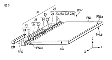
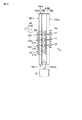
図1は、第1実施形態に係る表示装置DSPの一構成例を示す図である。
図示した例において、第1方向Xは、表示パネルPNLの短辺方向である。また、第2方向Yは、表示パネルPNLの長辺方向であり、第1方向Xと直交する方向である。また、第3方向Zは、第1方向Xおよび第2方向Yと直交する方向であり、表示パネルPNLの法線方向である。なお、第1方向X、第2方向Y、および第3方向Zは、互いに直交する方向に限定されるものではなく、互いに90°以外の角度で交差していてもよい。
FIG. 1 is a diagram illustrating a configuration example of the display device DSP according to the first embodiment.
In the illustrated example, the first direction X is the short side direction of the display panel PNL. The second direction Y is a long side direction of the display panel PNL and is a direction orthogonal to the first direction X. Further, the third direction Z is a direction orthogonal to the first direction X and the second direction Y, and is the normal direction of the display panel PNL. The first direction X, the second direction Y, and the third direction Z are not limited to directions orthogonal to each other, and may intersect with each other at an angle other than 90°.
図示した例において、表示装置DSPは、光透過性を有する表示パネルPNLと、表示パネルPNLを照明する光源ユニットLUと、を備えている。表示パネルPNLは、画像を表示する表示領域DAと、表示領域DAの周囲に位置する非表示領域NDAと、を備えている。表示パネルPNLは、例えば、四角形状のパネルであり、表面に相当する一方の主面PNLaと、裏面に相当する他方の主面PNLbと、主面PNLaおよびPNLbと交差する側面PNLcおよびPNLdと、を備えている、主面PNLaと主面PNLbとは、互いに第3方向Zで対向している。側面PNLcと側面PNLdとは、互いに第2方向Yで対向している。 In the illustrated example, the display device DSP includes a light-transmissive display panel PNL and a light source unit LU that illuminates the display panel PNL. The display panel PNL includes a display area DA for displaying an image and a non-display area NDA located around the display area DA. The display panel PNL is, for example, a rectangular panel, and has one main surface PNLa corresponding to the front surface, the other main surface PNLb corresponding to the back surface, and side surfaces PNLc and PNLd intersecting with the main surfaces PNLa and PNLb. The main surface PNLa and the main surface PNLb, which are provided with, are opposed to each other in the third direction Z. The side surface PNLc and the side surface PNLd face each other in the second direction Y.
光源ユニットLUは、表示パネルPNLの内部を照明するものである。光源ユニットLUは、表示装置DSPの表示領域DAにおける透明性を確保する観点から、表示領域DAと第3方向Zで対向する位置の外側に位置している。図示した例では、光源ユニットLUは、側面PNLcと第2方向Yで対向しており、側面PNLcに向かって光を出射し、光変調層OMを照明する。なお、光源ユニットLUは、1つに限定されるものではなく、2つ以上が配置されてもよく、例えば側面PNLcおよびPNLdのそれぞれに対向配置されていてもよい。光源ユニットLUは、必ずしも側面PNLcと第2方向Yで対向していなくてもよく、例えば、表示パネルPNLの法線方向に対して斜めの位置に配置され、主面PNLbに向かって光を出射するものであってもよい。 The light source unit LU illuminates the inside of the display panel PNL. The light source unit LU is located outside the position facing the display area DA in the third direction Z from the viewpoint of ensuring transparency in the display area DA of the display device DSP. In the illustrated example, the light source unit LU faces the side surface PNLc in the second direction Y, emits light toward the side surface PNLc, and illuminates the light modulation layer OM. The number of light source units LU is not limited to one, and two or more light source units LU may be arranged, for example, the light source units LU may be arranged to face each of the side surfaces PNLc and PNLd. The light source unit LU does not necessarily have to face the side surface PNLc in the second direction Y. For example, the light source unit LU is arranged at an oblique position with respect to the normal direction of the display panel PNL and emits light toward the main surface PNLb. It may be one that does.
表示パネルPNLは、第1基板SUB1、第2基板SUB2、および光変調層OMを備えている。第1基板SUB1および第2基板SUB2は、それぞれ光透過性を有している。第1基板SUB1および第2基板SUB2は、互いに第3方向Zで対向しており、第1基板SUB1は主面PNLa側に配置され、第2基板SUB2は主面PNLb側に配置されている。光変調層OMは、第1基板SUB1と第2基板SUB2との間に位置している。光変調層OMは、表示領域DAの一部または全部において、光透過性を有する状態と、光散乱性を有する状態と、を可逆的に切り替えることができる。すなわち、光変調層OMは、光散乱性の強度を変調することができる。 The display panel PNL includes a first substrate SUB1, a second substrate SUB2, and a light modulation layer OM. The first substrate SUB1 and the second substrate SUB2 each have optical transparency. The first substrate SUB1 and the second substrate SUB2 face each other in the third direction Z, the first substrate SUB1 is arranged on the main surface PNLa side, and the second substrate SUB2 is arranged on the main surface PNLb side. The light modulation layer OM is located between the first substrate SUB1 and the second substrate SUB2. The light modulation layer OM can reversibly switch between a light-transmitting state and a light-scattering state in part or all of the display area DA. That is, the light modulation layer OM can modulate the intensity of light scattering.
表示領域DAには、複数の主画素PX(PX11、…、PXnm)が配置されている。主画素PXは、表示の最小単位に相当する。例えば、主画素PX11を基準にすると、主画素PX11、…、PXn1が、この順で第1方向Xに並んでいる。また、主画素PX11、…、PX1mが、この順で第2方向Yに並んでいる。主画素PX11は側面PNLdに近接する側に位置し、主画素PX1mは、側面PNLcに近接する側に位置している。主画素PXxyは、図示した例では、4つの副画素PAxy、PBxy、PCxy、およびPDxyを備えている。なお、xは、1〜nの正の整数であり、yは、1〜mの正の整数である。以下の説明において、副画素PAxy、PBxy、PCxy、およびPDxyを、それぞれ総称して、副画素PA、PB、PC、およびPDと称する場合がある。 A plurality of main pixels PX (PX11,..., PXnm) are arranged in the display area DA. The main pixel PX corresponds to the minimum display unit. For example, based on the main pixel PX11, the main pixels PX11,..., PXn1 are arranged in this order in the first direction X. Further, the main pixels PX11,..., PX1m are arranged in this order in the second direction Y. The main pixel PX11 is located on the side close to the side surface PNLd, and the main pixel PX1m is located on the side close to the side surface PNLc. In the illustrated example, the main pixel PXxy includes four sub-pixels PAxy, PBxy, PCxy, and PDxy. In addition, x is a positive integer of 1 to n, and y is a positive integer of 1 to m. In the following description, the subpixels PAxy, PBxy, PCxy, and PDxy may be collectively referred to as subpixels PA, PB, PC, and PD, respectively.
主画素PXxyは例えば四角形状であり、副画素PAxyは、第1方向Xで副画素PBxyと隣り合い、第2方向Yで副画素PDxyと隣り合っている。副画素PCxyは、主画素PXxyにおける副画素PAxyの対角に位置し、第1方向Xで副画素PDxyと隣り合い、第2方向Yで副画素PBxyと隣り合っている。但し、副画素PA、PB、PC、およびPDは、互いの位置関係を上記に限定されるものではなく、互いの位置が入れ替わっていてもよい。 The main pixel PXxy has, for example, a quadrangular shape, and the sub pixel PAxy is adjacent to the sub pixel PBxy in the first direction X and is adjacent to the sub pixel PDxy in the second direction Y. The sub-pixel PCxy is located diagonally to the sub-pixel PAxy in the main pixel PXxy, is adjacent to the sub-pixel PDxy in the first direction X, and is adjacent to the sub-pixel PBxy in the second direction Y. However, the positional relationship between the sub-pixels PA, PB, PC, and PD is not limited to the above, and their positions may be interchanged.
副画素PAxyに対応する領域には、カラーフィルタFAxyが配置されている。同様に、副画素PBxyに対応する領域にカラーフィルタFBxyが配置され、副画素PCxyに対応する領域にカラーフィルタFCxyが配置され、副画素PDxyに対応する領域にカラーフィルタFDxyが配置されている。各カラーフィルタFAxy、FBxy、FCxy、およびFDxyは、例えば、それぞれ、第2基板SUB2の副画素PAxy乃至PDxyに配置されている。すなわち、主画素PXxyは、カラーフィルタFAxy、FBxy、FCxy、およびFDxyを備えている。カラーフィルタFAxy、FBxy、FCxy、およびFDxyの互いの位置関係は、副画素PAxy、PBxy、PCxy、およびPDxyの互いの位置関係と同様である。なお、以下の説明において、カラーフィルタFAxy、FBxy、FCxy、およびFDxyを、それぞれ総称して、カラーフィルタFA、FB、FC、およびFDと称する場合がある。 A color filter FAxy is arranged in the area corresponding to the sub-pixel PAxy. Similarly, the color filter FBxy is arranged in the area corresponding to the sub-pixel PBxy, the color filter FCxy is arranged in the area corresponding to the sub-pixel PCxy, and the color filter FDxy is arranged in the area corresponding to the sub-pixel PDxy. The color filters FAxy, FBxy, FCxy, and FDxy are respectively arranged in the sub-pixels PAxy to PDxy of the second substrate SUB2, for example. That is, the main pixel PXxy includes color filters FAxy, FBxy, FCxy, and FDxy. The positional relationship between the color filters FAxy, FBxy, FCxy, and FDxy is similar to that between the sub-pixels PAxy, PBxy, PCxy, and PDxy. In the following description, the color filters FAxy, FBxy, FCxy, and FDxy may be collectively referred to as color filters FA, FB, FC, and FD, respectively.
一例では、副画素PAは、主面PNLaに赤色を表示するレッド(R)画素であり、カラーフィルタFAは、赤色光を透過させるレッド(R)カラーフィルタである。また、副画素PBは、主面PNLaに緑色光を表示するグリーン(G)画素であり、カラーフィルタFBは、緑色を透過させるグリーン(G)カラーフィルタである。また、副画素PCは、主面PNLaに青色を表示するブルー(B)画素であり、カラーフィルタFCは、青色光を透過させるブルー(B)カラーフィルタである。カラーフィルタFA、FB、およびFCは、図示した例では第2基板SUB2に配置されているが、これに限定されるものではなく、例えば第1基板SUB1に配置されてもよい。
一例では、副画素PDは、主面PNLaに黒色を表示するブラック(N)画素であり、カラーフィルタFDは、白色光を吸収するブラック(N)カラーフィルタである。このとき、副画素PDはダミー画素に相当し、カラーフィルタFDは光吸収層に相当する。カラーフィルタFDは、第2基板SUB2側に配置されているため、副画素PDは、駆動時に主面PNLbに白色を表示することができる。ダミー画素は、図示した例では主画素PXに含まれているが、例えば、主画素PXから独立して配置され、主画素PXの間に位置してもよい。
但し、副画素PA、PB、およびPCが表示する色は、上記に限定されるものではなく、それぞれ、互いに異なる第1乃至第3色であればよい。また、副画素PDが表示する色も、黒色に限定されるものではなく、第1乃至第3色よりも明度の低い第4色であればよい。この場合、カラーフィルタFA乃至FCは、それぞれ、第1乃至第3色を透過させるものであり、カラーフィルタFDは、カラーフィルタFA乃至FCよりも透過率が低く、第4色を透過させるものである。
In one example, the sub-pixel PA is a red (R) pixel that displays red on the main surface PNLa, and the color filter FA is a red (R) color filter that transmits red light. The sub-pixel PB is a green (G) pixel that displays green light on the main surface PNLa, and the color filter FB is a green (G) color filter that transmits green. The sub-pixel PC is a blue (B) pixel that displays blue on the main surface PNLa, and the color filter FC is a blue (B) color filter that transmits blue light. Although the color filters FA, FB, and FC are arranged on the second substrate SUB2 in the illustrated example, the invention is not limited to this, and may be arranged on the first substrate SUB1, for example.
In one example, the sub-pixel PD is a black (N) pixel that displays black on the main surface PNLa, and the color filter FD is a black (N) color filter that absorbs white light. At this time, the sub-pixel PD corresponds to a dummy pixel, and the color filter FD corresponds to a light absorption layer. Since the color filter FD is arranged on the second substrate SUB2 side, the sub-pixel PD can display white on the main surface PNLb during driving. The dummy pixel is included in the main pixel PX in the illustrated example, but may be arranged independently of the main pixel PX and may be located between the main pixels PX, for example.
However, the colors displayed by the sub-pixels PA, PB, and PC are not limited to the above, and may be first to third colors different from each other. Further, the color displayed by the sub-pixel PD is not limited to black, and may be the fourth color having a lower brightness than the first to third colors. In this case, the color filters FA to FC respectively transmit the first to third colors, and the color filter FD has a lower transmittance than the color filters FA to FC and transmits the fourth color. is there.
なお、複数の主画素PXのうち少なくとも1つの画素において、副画素PA、PB、PCおよびPDのいずれか1つが白色を表示するホワイト(W)画素であってもよい。W画素に配置されるカラーフィルタは、白色光を透過させるホワイト(W)カラーフィルタである。但し、ここでいうW画素は、白色を表示するものに限定されるものではなく、第1乃至第3色よりも明度の高い第5色を表示するものであればよい。この場合、Wカラーフィルタは、表示パネルPNLを透過する光の色味を調整する目的で、薄く色付いた光を透過させるものであってもよい。 Note that in at least one pixel of the plurality of main pixels PX, any one of the sub-pixels PA, PB, PC, and PD may be a white (W) pixel that displays white. The color filter arranged in the W pixel is a white (W) color filter that transmits white light. However, the W pixel here is not limited to the one that displays white, and may be any pixel that displays the fifth color having a higher brightness than the first to third colors. In this case, the W color filter may transmit light colored light for the purpose of adjusting the tint of light transmitted through the display panel PNL.
R、G、B、およびNカラーフィルタは、例えば、それぞれ赤色、緑色、青色、および黒色の色材によって着色された樹脂によって形成される。Wカラーフィルタは、無着色の透明な樹脂、または薄く着色された樹脂によって形成される。また、W画素は、白色を表示できればそれでよいため、Wカラーフィルタは、省略されてもよい。 The R, G, B, and N color filters are formed of, for example, resins colored with red, green, blue, and black color materials, respectively. The W color filter is formed of an uncolored transparent resin or a lightly colored resin. In addition, the W color filter may be omitted as long as it can display white.
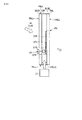
図2は、図1に示した第1基板SUB1の一構成例を示す図である。
図示した表示パネルPNLは、いわゆるアクティブマトリクス型の表示パネルである。第1基板SUB1は、表示領域DAに対応する領域に複数の電極を有し、非表示領域NDAに対応する領域に駆動部DRを備えている。
FIG. 2 is a diagram showing a configuration example of the first substrate SUB1 shown in FIG.
The illustrated display panel PNL is a so-called active matrix type display panel. The first substrate SUB1 has a plurality of electrodes in an area corresponding to the display area DA, and has a drive unit DR in an area corresponding to the non-display area NDA.
副画素PAxyに対応する領域に、電極EAxyが配置されている。同様に、副画素PBxyに対応する領域に電極EBxyが配置され、副画素PCxyに対応する領域に電極ECxyが配置され、副画素PDxyに対応する領域に電極EDxyが配置されている。すなわち、主画素PXxyには、電極EAxy、EBxy、ECxy、およびEDxyが配置されている。また、電極EAxyは、図1に示したカラーフィルタFAxyと対向し、電極EBxyは、図1に示したカラーフィルタFBxyと対向し、電極ECxyは、図1に示したカラーフィルタFCxyと対向し、電極EDxyは、図1に示したカラーフィルタFDxyと対向している。なお、以下の説明において、電極EAxy、EBxy、ECxy、およびEDxyを、それぞれ総称して、電極EA、EB、EC、およびEDと称する場合がある。 The electrode EAxy is arranged in a region corresponding to the subpixel PAxy. Similarly, the electrode EBxy is arranged in a region corresponding to the sub-pixel PBxy, the electrode ECxy is arranged in a region corresponding to the sub-pixel PCxy, and the electrode EDxy is arranged in a region corresponding to the sub-pixel PDxy. That is, the electrodes EAxy, EBxy, ECxy, and EDxy are arranged in the main pixel PXxy. The electrode EAxy faces the color filter FAxy shown in FIG. 1, the electrode EBxy faces the color filter FBxy shown in FIG. 1, the electrode ECxy faces the color filter FCxy shown in FIG. The electrode EDxy faces the color filter FDxy shown in FIG. In the following description, the electrodes EAxy, EBxy, ECxy, and EDxy may be collectively referred to as electrodes EA, EB, EC, and ED, respectively.
駆動部DRは、第1ドライバDr1および第2ドライバDr2を備えている。第1ドライバDr1は、画像を表示するためのデータ信号を電極EA乃至EDに供給するデータ線駆動回路に相当する。第1ドライバDr1からは、i本のデータ線S(S1、S2、…、Si)が表示領域DAに向かい引き出されている。複数のデータ線Sは、表示領域DAにおいて、例えば、第2方向Yに延在し、第1方向Xに並んでいる。第2ドライバDr2は、電極EA乃至EDへのデータ信号の入力を制御する走査信号を供給する走査線駆動回路に相当する。第2ドライバDr2からは、j本の走査線G(G1、G2、…、Gj)が表示領域DAに向かい引き出されている。複数の走査線Gは、表示領域DAにおいて、例えば、第1方向Xに延在し、第2方向Yに並んでいる。一例として、データ線S1は、画素電極EA11、EB11、…、EAn1、EBn1のそれぞれにデータ信号を伝達する。また、走査線G1は、画素電極EA11、ED11、…、EA1m、ED1mのそれぞれに走査信号を伝達する。但し、データ線Sおよび走査線Gの延在方向は、特に限定されるものではなく、それぞれ一部が屈曲していてもよい。また、データ線Sが第1方向Xに延在し、走査線Gが第2方向Yに延在していてもよい。 The drive unit DR includes a first driver Dr1 and a second driver Dr2. The first driver Dr1 corresponds to a data line drive circuit that supplies a data signal for displaying an image to the electrodes EA to ED. From the first driver Dr1, i data lines S (S1, S2,..., Si) are drawn out toward the display area DA. In the display area DA, the plurality of data lines S extend in the second direction Y and are arranged in the first direction X, for example. The second driver Dr2 corresponds to a scanning line driving circuit that supplies a scanning signal that controls the input of the data signal to the electrodes EA to ED. From the second driver Dr2, j scanning lines G (G1, G2,..., Gj) are drawn toward the display area DA. In the display area DA, the plurality of scanning lines G extend in the first direction X and are arranged in the second direction Y, for example. As an example, the data line S1 transmits a data signal to each of the pixel electrodes EA11, EB11,..., EAn1, EBn1. Further, the scanning line G1 transmits a scanning signal to each of the pixel electrodes EA11, ED11,..., EA1m, ED1m. However, the extending direction of the data line S and the scanning line G is not particularly limited, and a part of each may be bent. Further, the data line S may extend in the first direction X and the scanning line G may extend in the second direction Y.
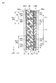
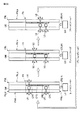
図3は、図1に示した表示パネルPNLの一構成例を示す断面図である。
なお、本図に示した断面は、第2方向Yに隣り合う主画素PX11およびPX13を含む領域であり、副画素PAおよびPDを含む第2方向Yに沿った断面の一例である。主画素PX11には、カラーフィルタFA11、FD11、および電極EA11、ED11が配置され、主画素PX13には、カラーフィルタFA13、FD13および電極EA13、ED13が配置されている。
FIG. 3 is a cross-sectional view showing a configuration example of the display panel PNL shown in FIG.
The cross section shown in the figure is a region including the main pixels PX11 and PX13 adjacent to each other in the second direction Y, and is an example of a cross section including the sub-pixels PA and PD along the second direction Y. Color filters FA11, FD11 and electrodes EA11, ED11 are arranged in the main pixel PX11, and color filters FA13, FD13 and electrodes EA13, ED13 are arranged in the main pixel PX13.
第1基板SUB1は、絶縁基板10、電極EA11、ED11、EA13、ED13、および配向膜AL1を備えている。絶縁基板10は、光透過性を有するガラス基板や樹脂基板によって形成されている。電極EA11、ED11、EA13、およびED13は、絶縁基板10の第2基板SUB2に近接する側に配置され、第2方向Yに沿ってこの順に並んでいる。電極EA11、ED11、EA13、およびED13は、互いに第2方向Yに離間している。そして、電極ED11と電極EA13との間隔は、電極EA11と電極ED11との間隔よりも大きい。電極EA、EDは、透明導電材料によって形成されており、例えば、インジウム錫酸化物(ITO)やインジウム亜鉛酸化物(IZO)によって形成されている。配向膜AL2は、絶縁基板10、および電極EA、EDの第2基板SUB2に近接する側に配置されており、例えば電極EA、EDを覆っている。
The first substrate SUB1 includes an insulating
第2基板SUB2は、絶縁基板20、カラーフィルタFA11、FD11、FA13、FD13、オーバーコート層OC、共通電極CE、および配向膜AL2を備えている。また、図示した例では、複数の光反射層RFを備えている。絶縁基板20は、光透過性を有するガラス基板や樹脂基板によって形成されている。
The second substrate SUB2 includes an insulating
カラーフィルタFA11、FD11、FA13、およびFD13は、絶縁基板20の第1基板SUB1に近接する側に配置され、それぞれ電極EA11、ED11、EA13、およびED13と第3方向Zで対向している。カラーフィルタFA11とカラーフィルタFD11とは、第2方向YにおいてピッチPT1で隣り合っており、図示した例では互いに接触している。カラーフィルタFD11とカラーフィルタFA13とは、第2方向YにおいてピッチPT1よりも大きいピッチPT2で隣り合い、互いに離間している。カラーフィルタFD11とカラーフィルタFA13との間には、例えばオーバーコート層OCが位置している。カラーフィルタFA13とカラーフィルタFD13とも、第2方向YにおいてピッチPT1で隣り合っている。なお、ここで言うピッチとは、隣り合う夫々のカラーフィルタの中心同士の間隔を意味するものとする。但し、ピッチとは、隣り合う夫々のカラーフィルタの第2方向Yの矢印が位置する側(またはその反対側)の端部同士の間隔を意味するものであってもよい。つまり、ピッチPT1は、電極EA11の中心と電極ED11の中心との第2方向Yにおける間隔に相当する。また、ピッチPT2は、電極ED11の中心と電極EA13の中心との第2方向Yにおける間隔に相当する。
The color filters FA11, FD11, FA13, and FD13 are arranged on the side of the insulating
図示した例では、カラーフィルタFDが光吸収層に相当し、光吸収層と光変調層OMとの間に、光反射層RFが配置されている。光反射層RFは、カラーフィルタFDの主面PNLb側に配置されていればよい。光反射層RFは、光反射性の高い金属材料によって形成されており、主面PNLa側へ向かう光を主面PNLb側へ反射する。従って、ダミー画素に相当する副画素PDの主画素PNLa側の輝度を抑制し、主画素PNLb側の輝度を向上させることができる。第2基板SUB2に光反射層RFが配置されている場合、ダミー画素の光変調層OMから主面PNLaへの光は光反射層RFが遮光することができる。このため、カラーフィルタFDは、Nカラーフィルタに限定されず、黒色よりも明度の高い色であってもよい。カラーフィルタFDは、光反射層RFのカラーフィルタFD側での反射光を低減できる色であれば、主面PNLaに表示される画像のぎらつきを抑制することができる。 In the illustrated example, the color filter FD corresponds to the light absorption layer, and the light reflection layer RF is arranged between the light absorption layer and the light modulation layer OM. The light reflection layer RF may be arranged on the main surface PNLb side of the color filter FD. The light reflection layer RF is formed of a metal material having high light reflectivity, and reflects light traveling toward the main surface PNLa toward the main surface PNLb. Therefore, it is possible to suppress the luminance on the main pixel PNLa side of the sub-pixel PD corresponding to the dummy pixel and improve the luminance on the main pixel PNLb side. When the light reflection layer RF is arranged on the second substrate SUB2, the light reflection layer RF can block the light from the light modulation layer OM of the dummy pixel to the main surface PNLa. Therefore, the color filter FD is not limited to the N color filter and may be a color having a lightness higher than black. The color filter FD can suppress the glare of the image displayed on the main surface PNLa as long as the color can reduce the reflected light on the color filter FD side of the light reflection layer RF.
オーバーコート層OCは、絶縁基板20およびカラーフィルタFA、FDの第1基板SUB1に近接する側に配置され、例えばカラーフィルタFAおよび光反射層RFを覆っている。もしもカラーフィルタFD11がWカラーフィルタであるとすると、カラーフィルタFD11は省略され、カラーフィルタFD11の位置にはオーバーコート層が配置されていてもよい。
The overcoat layer OC is disposed on the side of the insulating
共通電極CEは、オーバーコート層OCの第1基板SUB1に近接する側に配置され、例えばオーバーコート層OCを覆っている。共通電極CEは、第3方向Zで複数の電極EA11、EA13、ED11、およびED13と対向している。また、共通電極CEは、主画素PX11と主画素PX13との間の領域にも延在しており、電極ED11と電極EA13との間の領域にも配置されている。共通電極CEは、ITOやIZOなどの透明導電材料によって形成されている。配向膜AL2は、共通電極CEの第1基板SUB1と対向する側に配置され、例えば共通電極CEを覆っている。 The common electrode CE is arranged on the side of the overcoat layer OC that is close to the first substrate SUB1 and covers the overcoat layer OC, for example. The common electrode CE faces the plurality of electrodes EA11, EA13, ED11, and ED13 in the third direction Z. The common electrode CE also extends in the region between the main pixels PX11 and PX13, and is also arranged in the region between the electrodes ED11 and EA13. The common electrode CE is made of a transparent conductive material such as ITO or IZO. The alignment film AL2 is arranged on the side of the common electrode CE facing the first substrate SUB1 and covers the common electrode CE, for example.
光変調層OMは、第1基板SUB1と第2基板SUB2との間に位置し、配向膜AL1およびAL2に隣接している。光変調層OMは、電極EA、EB、EC、およびEDのそれぞれによって生じる電場の大きさや向きに応じて、副画素PA、PB、PC、およびPDのそれぞれに対応する領域の光散乱性を変調することができる。例えば、光変調層OMは、電極EAに電圧が印加されていない時にカラーフィルタFAに対応する領域に入射する光を散乱させ、電極EAに電圧が印加されている時にカラーフィルタFAに対応する領域に入射する光を透過させる。光変調層OMは、例えば、バルク31と、バルク31内に分散配置された複数の微粒子32とを含んだ複合層となっている。微粒子32は第1領域に相当し、バルク31は第2領域に相当する。
The light modulation layer OM is located between the first substrate SUB1 and the second substrate SUB2 and is adjacent to the alignment films AL1 and AL2. The light modulation layer OM modulates the light scattering properties of the regions corresponding to the sub-pixels PA, PB, PC, and PD according to the magnitude and direction of the electric field generated by each of the electrodes EA, EB, EC, and ED. can do. For example, the light modulation layer OM scatters light that is incident on the area corresponding to the color filter FA when the voltage is not applied to the electrode EA, and the area corresponding to the color filter FA when the voltage is applied to the electrode EA. Allows incident light to pass through. The light modulation layer OM is, for example, a composite layer including a
バルク31および微粒子32は、光学率異方性を有している。例えば、微粒子32に含まれる液晶材料(後述する液晶分子LM)の屈折率異方性の大きさは、バルク31の高分子材料を構成するモノマーの屈折率異方性の大きさと等しい。また、バルク31および微粒子32は、電場に対する応答速度が互いに異なっている。例えば、バルク31は、電場に対して応答しない筋状構造もしくは多孔質構造となっている。または、バルク31は、微粒子32の応答速度よりも遅い応答速度を有する筋状構造もしくは棒状構造となっている。バルク31は、例えば、配向性および重合性を有する低分子のモノマーを熱および光の少なくとも一方によって重合化することにより得られる固形の高分子材料によって構成されている。一方、微粒子32は、例えば、液晶材料を主に含んで構成されており、バルク31よりも分子自由度の高い液状である。つまり、微粒子32は、バルク31の応答速度よりも十分に早い応答速度を有している。
The
バルク31のモノマーや微粒子32の液晶材料は、配向膜AL1およびAL2から配向規制力を受けて配向する。配向膜AL1およびAL2は、垂直配向膜や水平配向膜であるが、モノマーや液晶材料を配向させるものであれば特に限定されるものではなく、例えばポリイミドやポリアミドイミドによって形成される。モノマーが配向した状態で重合されることで、バルク31(高分子材料)の分子配向が固定化される。なお、配向膜AL1およびAL2を用いることなくモノマーを配向させることが可能な場合には、配向膜AL1およびAL2は省略されてもよい。例えば、電極EAと共通電極CEとの間、または電極EDと共通電極CEとの間に電場や磁場を印加することによっても、光変調層OMに用いられる液晶材料やモノマーを配向させることが可能である。つまり、電極EA(EB、EC、およびED)と共通電極CEとの間に電場や磁場を印加させながらモノマーを重合することで、バルク31(高分子材料)の分子配向を固定化することができる。液晶材料やモノマーの配向に電場を用いる場合には、配向用と駆動用とで別々の電極を形成するか、液晶材料に周波数によって誘電率異方性の符号が反転する二周波液晶などを用いることができる。また、液晶材料やモノマーの配向に磁場を用いる場合、液晶材料やモノマーとして磁化率異方性の大きい材料を用いることが好ましく、例えば、ベンゼン環の多い材料を用いることが好ましい。
The monomer of the
バルク31を形成する配向性および重合性を有するモノマーとしては、光学的に異方性を有しており、かつ液晶と複合する材料であればよいが、本実施の形態では紫外線で硬化する低分子モノマーであることが好ましい。微粒子32として液晶材料が用いられる場合に、その液晶材料が棒状分子であるときには、使用するモノマー材料の形状も棒状であることが好ましい。以上のことから、モノマー材料としては重合性と液晶性を併せ持つ材料を用いることが好ましく、例えば、重合性官能基として、アクリレート基、メタクリレート基、アクリロイルオキシ基、メタクリロイルオキシ基、ビニルエーテル基およびエポキシ基からなる群から選ばれた少なくとも1つの官能基を有することが好ましい。これらの官能基は、紫外線、赤外線または電子線を照射したり、加熱したりすることによって重合させることができる。紫外線照射時の配向度低下を抑制するために、多官能基をもつ液晶性材料を添加することもできる。バルク31を上述した筋状構造とする場合には、バルク31の原料として、2官能液晶性モノマーを用いることが好ましい。また、バルク31の原料に対して、液晶性を示す温度の調整を目的に単官能モノマーを添加したり、架橋密度向上を目的に3官能以上のモノマーを添加したりすることもできる。
As the monomer having the orientation and the polymerizability for forming the
ところで、光変調層OMで散乱された光は、主面PNLa側と主面PNLb側との両方に向かって散乱される。従って、上記の様な、R、G、B、およびNカラーフィルタが第2基板SUB2に配置されている構成では、駆動時(後述する散乱モード)のR画素は、主面PNLaに赤色を表示すると共に、主面PNLbに薄い赤色を表示する。これは、R画素の光変調層OMにおいて主面PNLaへ向かって散乱された光の一部が、Rカラーフィルタを透過した後に第2基板SUB2の各部材の界面で反射されて主面PNLbへ向かうためである。第2基板SUB2での反射光が弱い場合、駆動時のR画素は、主面PNLbに白色を表示する。同様に、駆動時のG画素も、主面PNLbに薄い緑色または白色を表示し、駆動時のB画素も、主面PNLbに薄い青色または白色を表示する。駆動時のダミー画素は、主面PNLbに白色を表示する。 By the way, the light scattered by the light modulation layer OM is scattered toward both the main surface PNLa side and the main surface PNLb side. Therefore, in the configuration in which the R, G, B, and N color filters are arranged on the second substrate SUB2 as described above, the R pixel at the time of driving (scattering mode described later) displays red on the main surface PNLa. At the same time, a light red color is displayed on the main surface PNLb. This is because a part of the light scattered toward the principal surface PNLa in the light modulation layer OM of the R pixel is reflected by the interface of each member of the second substrate SUB2 after passing through the R color filter and is directed to the principal surface PNLb. The reason is to go. When the reflected light on the second substrate SUB2 is weak, the R pixel during driving displays white on the main surface PNLb. Similarly, the G pixel during driving also displays a light green or white color on the main surface PNLb, and the B pixel during driving also displays a light blue or white color on the main surface PNLb. The driven dummy pixel displays white on the main surface PNLb.
図4は、図1に示した表示パネルPNLの他の構成例を示す断面図である。
図示した構成例は、共通電極CEが不連続である点で、図3に示した構成例と相違している。すなわち、共通電極CEは、互いに第2方向Yで離間する共通電極CE1およびCE2を備えている。
FIG. 4 is a cross-sectional view showing another configuration example of the display panel PNL shown in FIG.
The illustrated configuration example differs from the configuration example illustrated in FIG. 3 in that the common electrode CE is discontinuous. That is, the common electrode CE includes common electrodes CE1 and CE2 which are separated from each other in the second direction Y.
共通電極CE1は、電極EA11およびED11と対向している。共通電極CE2は、電極EA13およびED13と対向している。電極ED11と電極EA13との間の領域に対向する位置、すなわち主画素PX11と主画素PX13との間の領域には、共通電極CEが配置されていない。このため、主画素PX間の光透過率が向上し、表示パネルPNLの光透過率を向上させることができる。 The common electrode CE1 faces the electrodes EA11 and ED11. The common electrode CE2 faces the electrodes EA13 and ED13. The common electrode CE is not arranged at a position facing the area between the electrode ED11 and the electrode EA13, that is, in the area between the main pixel PX11 and the main pixel PX13. Therefore, the light transmittance between the main pixels PX is improved, and the light transmittance of the display panel PNL can be improved.
図5は、図1に示した表示パネルPNLの他の構成例を示す断面図である。
図示した構成例は、複数の遮光層BMを備えている点で、図3に示した構成例と相違している。遮光層BMは、遮光性を有しており、例えば黒色樹脂や黒色金属によって形成されている。遮光層BMは、絶縁基板20の第1基板SUB1と対向する側に配置されている。複数の遮光層BMは、それぞれ、カラーフィルタFA11、FD11、FA13、およびFD13の第2方向Yにおける端部と、第3方向Zで対向している。また、遮光層BMは、例えば、電極EA11、ED11、EA13、およびED13の第2方向Yにおける端部と、第3方向Zで対向していてもよい。遮光層BMは、図示しないデータ線Sや走査線Gと第3方向Zで対向し、配線における反射光を遮光することができる。また、1つの電極に対応する領域において変調された光が別の電極と第3方向Zで対向するカラーフィルタを透過することで生じる混色を抑制することができる。
FIG. 5 is a cross-sectional view showing another configuration example of the display panel PNL shown in FIG.
The illustrated configuration example is different from the configuration example shown in FIG. 3 in that it includes a plurality of light shielding layers BM. The light shielding layer BM has a light shielding property and is formed of, for example, black resin or black metal. The light shielding layer BM is arranged on the side of the insulating
図6は、図1に示した光源ユニットLUの一構成例を示す図である。
光源ユニットLUは、例えば、複数の光源23を第2方向Yに一列に配置して構成されている。各光源23は、側面PNLcに向かって光を射出するようになっており、例えば、側面PNLcとの対向面に発光スポットを有する発光素子からなる。そのような発光素子としては、例えば、発光ダイオード(LED;Light Emitting Diode)、またはレーザダイオード(LD;Laser Diode)などが挙げられる。
FIG. 6 is a diagram showing a configuration example of the light source unit LU shown in FIG.
The light source unit LU is configured by arranging a plurality of
複数の光源23は、例えば、互いに色の異なる光を出射する2個以上の光源23ごとに、共通の基板24上に配置されている。この場合、1つの基板24と、その基板24上に配置された複数の光源23とにより、光源ブロック25が構成されている。光源ブロック25は、例えば、白色光を照明可能に構成されている。図示した例では、光源ブロック25は、3つの光源23A、23B、および23Cを備えている。光源23A、23B、および23Cは、それぞれ、赤色光を出射するレッド(R)光源、緑色光を出射するグリーン(G)光源、青色光を出射するブルー(B)光源であり、全てを点灯することで、光源ブロック25を白色光源として機能させることができる。
The plurality of
基板24は、例えば、光源23、光源23の駆動を制御する駆動回路CM(後述する制御部100の一部)と、を電気的に接続する配線が形成された回路基板であり、各光源23は、この回路基板上に実装されている。共通の基板24上に配置された各光源23(光源ブロック25内の各光源23A、23B、23C)は、駆動回路CMによって互いに独立に駆動されるようになっているが、一括で(非独立に)駆動されるようになっていてもよい。また、互いに異なる基板24上に配置された光源23(各光源ブロック25内の光源23)は、例えば、駆動回路CMによって互いに独立に駆動されるようになっており、例えば、互いに異なる電流経路に接続されている。互いに異なる基板24上に設けられた光源23(各光源ブロック25内の光源23)は、例えば、駆動回路CMによって一括で(非独立に)駆動されるようになっていてもよい。各々の基板24に配置された複数の光源23A、複数の23B、および複数の23Cが、それぞれ一括で駆動されてもよい。
The
表示装置DSPは、図示した例では、外光Loutおよび照明光Linのうち少なくとも一方を利用することで主面PNLaに画像を表示する。外光Loutは、主面PNLbから表示パネルPNLに入射する光であり、例えば、太陽光や外部照明などの環境光に相当する。外光Loutの入射面は、主面PNLbである。照明光Linは、光源ユニットLUから表示パネルPNLに入射する光である。照明光Linの入射面は、例えば側面PNLcである。表示装置DSPは、画像の表示において、外光Loutまたは照明光Linのいずれか一方のみを利用する構成であってもよく、両方を利用する構成であってもよい。また、表示装置DSPは、外部環境に応じて、外光Loutおよび照明光Linを適宜選択して、画像を表示するものであってもよい。但し、表示装置DSPは、外光Loutのみを利用して画像を表示する構成であってもよく、この時には光源ユニットLUは省略される。
表示パネルPNLは、外光Loutまたは照明光Linを、表示領域DAの一部または全部で、透過または散乱させることで画像を表示する。光変調層OMが光散乱性を示す状態を散乱モードと呼び、光変調層OMが光散乱性を示さず散乱モードよりも光透過の高い状態と透過モードと呼ぶこととする。表示パネルPNLは、表示に寄与する副画素を散乱モードとし、表示に寄与しない副画素を透過モードとすることで、画像を表示する。図7および図8を参照して、光変調層OMの光散乱性の変化の原理を模式的に説明する。図7は、電場が形成されていない状態の光変調層OMを示し、図8は、電場が形成されている状態の光変調層OMを示している。
In the illustrated example, the display device DSP displays an image on the main surface PNLa by using at least one of the outside light Lout and the illumination light Lin. The external light Lout is light that enters the display panel PNL from the main surface PNLb and corresponds to, for example, ambient light such as sunlight or external lighting. The incident surface of the external light Lout is the main surface PNLb. The illumination light Lin is light that enters the display panel PNL from the light source unit LU. The incident surface of the illumination light Lin is, for example, the side surface PNLc. The display device DSP may use only one of the external light Lout and the illumination light Lin in displaying an image, or may use both of them. The display device DSP may display the image by appropriately selecting the outside light Lout and the illumination light Lin according to the external environment. However, the display device DSP may be configured to display an image using only the external light Lout, and at this time, the light source unit LU is omitted.
The display panel PNL displays an image by transmitting or scattering the external light Lout or the illumination light Lin in part or all of the display area DA. A state in which the light modulation layer OM exhibits a light scattering property is called a scattering mode, and a state in which the light modulation layer OM does not exhibit a light scattering property and has a higher light transmission than the scattering mode is called a transmission mode. The display panel PNL displays an image by setting sub-pixels that contribute to display in a scattering mode and sub-pixels that do not contribute to display in a transmissive mode. The principle of change in the light scattering property of the light modulation layer OM will be schematically described with reference to FIGS. 7 and 8. FIG. 7 shows the light modulation layer OM in a state where no electric field is formed, and FIG. 8 shows the light modulation layer OM in a state where an electric field is formed.
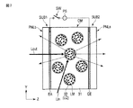
図7は、光変調層OMが散乱性を示す時の表示パネルPNLの模式図である。
ここでは、電源PSは共通電極CEと電気的に接続されているが、電極EAと電源PSとを結ぶ配線のスイッチSWが開いている。すなわち、電極EAに電圧が印加されておらず、電極EAと共通電極CEとの間に電位差が生じていない。
FIG. 7 is a schematic diagram of the display panel PNL when the light modulation layer OM exhibits a scattering property.
Here, the power supply PS is electrically connected to the common electrode CE, but the switch SW of the wiring connecting the electrode EA and the power supply PS is open. That is, no voltage is applied to the electrode EA, and there is no potential difference between the electrode EA and the common electrode CE.
微粒子32(液晶滴LQ)内に含まれる液晶材料(液晶分子LM)は、例えば棒状分子である。液晶分子LMは、液晶滴LQの中において、ランダムに配向している。この時、外光Loutおよび照明光Linに対するバルク31の屈折率と微粒子32の屈折率とは、互いに異なっている。従って、外光Loutおよび照明光Linは、バルク31と微粒子32との界面において屈折する。これにより、外光Loutおよび照明光Linは、光変調層OMにおいて散乱され、外光Loutおよび照明光Linの散乱光は、主面PNLaおよびPNLbから出射される。
The liquid crystal material (liquid crystal molecules LM) contained in the fine particles 32 (liquid crystal droplets LQ) is, for example, a rod-shaped molecule. The liquid crystal molecules LM are randomly aligned in the liquid crystal droplets LQ. At this time, the refractive index of the
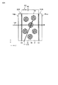
図8は、光変調層OMが透過性を示す時の表示パネルPNLの模式図である。
ここでは、スイッチSWが閉じており、電極EAに電源PSから電圧が印加され、電極EAと共通電極CEとの間に電位差が生じている。
FIG. 8 is a schematic diagram of the display panel PNL when the light modulation layer OM exhibits transparency.
Here, the switch SW is closed, a voltage is applied to the electrode EA from the power supply PS, and a potential difference is generated between the electrode EA and the common electrode CE.
図示した例では、液晶分子LMは、正の誘電率異方性を有する、いわゆるポジ型液晶である。このため、液晶分子LMは、液晶滴LQの中において、光変調層OMに形成される電場の方向である第3方向Zに配向する。この時、例えばバルク31を構成する高分子の屈折率異方性と液晶分子LMの屈折率異方性とが一致して、外光Loutおよび照明光Linに対するバルク31の屈折率と微粒子32の屈折率とが、互いに同等となる。従って、外光Loutは、光変調層OMを殆ど散乱されずに透過し、主面PNLaから出射される。また照明光Linも、光変調層OMを殆ど散乱されずに透過する。
以上説明した様に、光変調層OMは、電極EAへの印加電圧のオンオフ、すなわち光変調層OMに形成される電場の有無によって、光透過性と光散乱性とを切り替えることができる。
In the illustrated example, the liquid crystal molecule LM is a so-called positive type liquid crystal having positive dielectric anisotropy. Therefore, the liquid crystal molecules LM are aligned in the liquid crystal droplet LQ in the third direction Z, which is the direction of the electric field formed in the light modulation layer OM. At this time, for example, the refractive index anisotropy of the polymer that constitutes the
As described above, the light modulation layer OM can switch between the light transmission property and the light scattering property depending on whether the voltage applied to the electrode EA is on or off, that is, the presence or absence of an electric field formed in the light modulation layer OM.
なお、光変調層OMは、図7および図8において説明した構成では電場が形成されていない時に散乱性を示しているが、これは一例に過ぎず、電場が形成されている時に散乱性を示す構成であってもよい。電場が形成されている時に光変調層OMが散乱性を示す構成としては、例えば、バルク31が高分子の分子配向に沿って第2方向Yに延在する筋状構造を有し、液晶分子LMがバルク31の筋状構造に沿って配向する負の誘電率異方性を有するネガ型液晶である構成が考えられる。この様な構成においては、電場が形成されない時に、液晶分子LMが第2方向Yに配向し、バルク31と微粒子32との屈折率異方性が一致する。そして、電場が形成されている時に、液晶分子LMが第3方向Zに配向し、バルク31と微粒子32との屈折率異方性が相違する。
Although the light modulation layer OM exhibits the scattering property when the electric field is not formed in the configurations described in FIGS. 7 and 8, this is only an example, and the scattering property is generated when the electric field is formed. The configuration shown may be used. As a configuration in which the light modulation layer OM exhibits a scattering property when an electric field is formed, for example, the
以上の様に本構成例において、表示装置DSPは、外光Loutまたは照明光Linを透過または散乱させることで、画像を表示する。主画素PXは、R画素、B画素、G画素およびダミー画素を備えているため、主面PNLaに画像をカラー表示することができる。このとき、主面PNLbには反転画像がモノクロまたは薄いカラーで表示されるが、複数のダミー画素を不規則、または規則的(例えば格子状)に駆動することで、表示装置DSPは、主面PNLaに表示される画像の視認性を低下させることなく、主面PNLbに表示される反転画像の視認性を低下させることができる。 As described above, in the present configuration example, the display device DSP displays an image by transmitting or scattering the external light Lout or the illumination light Lin. Since the main pixel PX includes R pixels, B pixels, G pixels, and dummy pixels, an image can be displayed in color on the main surface PNLa. At this time, an inverted image is displayed on the main surface PNLb in monochrome or light color, but by driving a plurality of dummy pixels irregularly or regularly (for example, in a grid pattern), the display device DSP can It is possible to reduce the visibility of the reverse image displayed on the main surface PNLb without reducing the visibility of the image displayed on PNLa.
また、ダミー画素に光反射層RFが配置されている場合、ダミー画素の主面PNLb側の輝度が向上するため、主面PNLbに表示される反転画像の視認性をより低下させることができる。光吸収層がNカラーフィルタである場合、ダミー画素を駆動した際の主面PNLa側への光漏れを抑制することができるため、主面PNLaに表示される画像の表示品位の低下を抑制するこができる。 Further, when the light reflection layer RF is arranged in the dummy pixels, the brightness on the main surface PNLb side of the dummy pixels is improved, and thus the visibility of the reverse image displayed on the main surface PNLb can be further reduced. When the light absorption layer is the N color filter, it is possible to suppress light leakage to the main surface PNLa side when the dummy pixel is driven, and thus suppress deterioration of display quality of an image displayed on the main surface PNLa. I can do it.
また、上記の構成例では、R、G、Bカラーフィルタ、および光吸収層が第2基板SUB2に配置されているため、表示装置DSPは、主面PNLbから表示パネルPNLに入射する外光Loutを利用して画像を表示する場合だけではなく、側面PNLcから表示パネルPNLに入射する照明光Linを利用して画像を表示する場合でも、同様の効果を得ることができる。 Further, in the above configuration example, since the R, G, B color filters and the light absorption layer are arranged on the second substrate SUB2, the display device DSP causes the external light Lout incident on the display panel PNL from the main surface PNLb. The same effect can be obtained not only when an image is displayed by using, but also when an image is displayed by using the illumination light Lin that enters the display panel PNL from the side surface PNLc.
したがって、本実施形態によれば、裏面側からの情報取得が困難な表示装置を提供することができる。 Therefore, according to the present embodiment, it is possible to provide a display device in which it is difficult to obtain information from the back surface side.
表示装置DSPは、カラーフィルタの密度を変更することで、表示パネルPNLの透明性を変更するこができる。つまり、ピッチPT2をピッチPT1よりも大きく設定することにより、必要な解像度が得られる範囲で、表示パネルPNLの透過率を向上させることができる。また、ダミー画素の位置は、主画素PX内に限定されるものではなく、主画素PXの間であってもよい。このようなカラーフィルタの配置例について、以下に説明する。なお、以下の配置例では一例として、第1色のカラーフィルタはレッドカラーフィルタCFRとし、第2色のカラーフィルタはグリーンカラーフィルタCFGとし、第3色のカラーフィルタはブルーカラーフィルタCFBとし、第4色のカラーフィルタ(光吸収層)はブラックカラーフィルタCFNとし、第5色のカラーフィルタはホワイトカラーフィルタCFWとして説明するが、これらに限定されるものではく、第1色乃至第5色は、図1で説明した様な他の色であってもよい。第1乃至第5色のカラーフィルタの位置および面積は、それぞれ第1乃至第5色の副画素の位置および面積に相当する。このため、以下の説明において、R、G、B、N、Wカラーフィルタは、それぞれ、R、G、B、N、W画素と読み変えることが可能である。 The display device DSP can change the transparency of the display panel PNL by changing the density of the color filters. That is, by setting the pitch PT2 larger than the pitch PT1, it is possible to improve the transmittance of the display panel PNL in a range in which the required resolution can be obtained. The position of the dummy pixel is not limited to the position inside the main pixel PX, but may be between the main pixels PX. An example of the arrangement of such color filters will be described below. In the following arrangement example, the first color filter is the red color filter CFR, the second color filter is the green color filter CFG, and the third color filter is the blue color filter CFB. The four color filters (light absorption layers) are black color filters CFN, and the fifth color filters are white color filters CFW. However, the color filters are not limited to these, and the first to fifth colors are not limited to these. The color may be another color as described in FIG. The positions and areas of the color filters for the first to fifth colors correspond to the positions and areas of the sub-pixels for the first to fifth colors, respectively. Therefore, in the following description, the R, G, B, N, and W color filters can be read as R, G, B, N, and W pixels, respectively.
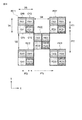
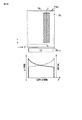
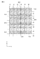
図9は、カラーフィルタの一配置例を示す図である。
主画素PX(PX11,PX31,PX22,PX13,PX33)は、それぞれ、図1に図示した様に、レッドカラーフィルタCFR、グリーンカラーフィルタCFG、ブルーカラーフィルタCFB、およびブラックカラーフィルタ(光吸収層)CFNを備えている。レッドカラーフィルタCFRは右下がりの斜線パターンで示す領域であり、グリーンカラーフィルタCFGは右上がりの斜線パターンで示す領域であり、ブルーカラーフィルタCFBは格子パターンで示す領域であり、ブラックカラーフィルタCFNはドットパターンで示す領域である。
FIG. 9 is a diagram showing an arrangement example of the color filters.
Each of the main pixels PX (PX11, PX31, PX22, PX13, PX33) has a red color filter CFR, a green color filter CFG, a blue color filter CFB, and a black color filter (light absorbing layer), as shown in FIG. Equipped with CFN. The red color filter CFR is a region shown by a diagonal line pattern in the lower right direction, the green color filter CFG is a region shown by a diagonal line pattern in the upper right direction, the blue color filter CFB is a region shown by a lattice pattern, and the black color filter CFN is This is an area indicated by a dot pattern.
図示した例において、主画素PXは、第2方向Yの幅W1、および第1方向Xの幅W3を有する四角形の画素である。主画素PX11および主画素PX31は、第1方向Xに沿った同一直線上に、間隔W4を空けて並んでいる。主画素PX11および主画素PX13は、第2方向Yに沿った同一直線上に、間隔W2を空けて並んでいる。つまり、主画素PX31のレッドカラーフィルタCFRと、主画素PX11のグリーンカラーフィルタCFGと、の互いに対向する側の端部は、間隔W4を空けて対向している。また、主画素PX13のグリーンカラーフィルタCFGと、主画素PX11のブルーカラーフィルタCFBと、の互いに対向する側の端部は、間隔W2を空けて対向している。なお、主画素PX13および主画素PX33も、第1方向Xに沿った同一直線上に、間隔W4を空けて並んでいる。主画素PX31および主画素PX33も、第2方向Yに沿った同一直線上に、間隔W2を空けて並んでいる。夫々の主画素PXの間の領域は、カラーフィルタの配置されていない透明な領域である。 In the illustrated example, the main pixel PX is a rectangular pixel having a width W1 in the second direction Y and a width W3 in the first direction X. The main pixel PX11 and the main pixel PX31 are arranged on the same straight line along the first direction X with an interval W4. The main pixels PX11 and PX13 are arranged on the same straight line along the second direction Y with an interval W2. That is, the ends of the red color filter CFR of the main pixel PX31 and the green color filter CFG of the main pixel PX11 on the opposite sides are opposed to each other with a space W4. Further, the green color filter CFG of the main pixel PX13 and the blue color filter CFB of the main pixel PX11 are opposed to each other with an interval W2 therebetween. The main pixel PX13 and the main pixel PX33 are also arranged on the same straight line along the first direction X with an interval W4. The main pixels PX31 and PX33 are also arranged on the same straight line along the second direction Y with a space W2. The area between the respective main pixels PX is a transparent area where no color filter is arranged.
一例では、間隔W4は、幅W3と等しく、間隔W2は、幅W1と等しい。つまり主画素PXは、それぞれ、第1方向Xおよび第2方向Yに、一画素分の間隔を空けて並んでいる。間隔W2は、幅W1よりも大きくてもよく、間隔W4は、幅W3よりも大きくてもよい。カラーフィルタのピッチという観点から見ると、互いに異なる画素に配置され第2方向Yに隣り合うカラーフィルタのピッチPT2は、同一画素内に配置され第2方向Yに隣り合うカラーフィルタのピッチPT1の3倍以上である。また、互いに異なる画素に配置され第1方向Xに隣り合うカラーフィルタのピッチPT4は、同一画素内に配置され第1方向Xに隣り合うカラーフィルタのピッチPT3の3倍以上である。 In one example, the spacing W4 is equal to the width W3 and the spacing W2 is equal to the width W1. That is, the main pixels PX are arranged in the first direction X and the second direction Y with a space of one pixel therebetween. Interval W2 may be greater than width W1 and interval W4 may be greater than width W3. From the viewpoint of the pitch of the color filters, the pitch PT2 of the color filters arranged in different pixels and adjacent to each other in the second direction Y is 3 of the pitch PT1 of the color filters arranged in the same pixel and adjacent to each other in the second direction Y. More than double. The pitch PT4 of the color filters arranged in different pixels and adjacent to each other in the first direction X is three times or more the pitch PT3 of the color filters arranged in the same pixel and adjacent to each other in the first direction X.
主画素PX22は、主画素PX11と主画素PX33との間に位置し、主画素PX31と主画素PX13との間に位置している。主画素PX22のレッドカラーフィルタCFRの角は、主画素PX11のブルーカラーフィルタCFBの角と隣接している。主画素PX22のグリーンカラーフィルタCFGの角は、主画素PX31のブラックカラーフィルタCFNの角と隣接している。主画素PX22のブルーカラーフィルタCFBの角は、主画素PX33のレッドカラーフィルタCFRの角と隣接している。主画素PX22のブラックカラーフィルタCFNの角は、主画素PX13のグリーンカラーフィルタCFGの角と隣接している。つまり、主画素PX22は、主画素PX11と主画素PX31との間、主画素PX11と主画素PX13との間、主画素PX33と主画素PX31との間、および、主画素PX33と主画素PX13との間、には位置していない。 The main pixel PX22 is located between the main pixels PX11 and PX33 and between the main pixels PX31 and PX13. The corner of the red color filter CFR of the main pixel PX22 is adjacent to the corner of the blue color filter CFB of the main pixel PX11. The corner of the green color filter CFG of the main pixel PX22 is adjacent to the corner of the black color filter CFN of the main pixel PX31. The corner of the blue color filter CFB of the main pixel PX22 is adjacent to the corner of the red color filter CFR of the main pixel PX33. The corner of the black color filter CFN of the main pixel PX22 is adjacent to the corner of the green color filter CFG of the main pixel PX13. That is, the main pixel PX22 includes the main pixel PX11 and the main pixel PX31, the main pixel PX11 and the main pixel PX13, the main pixel PX33 and the main pixel PX31, and the main pixel PX33 and the main pixel PX13. Not located in between.
この様な千鳥状に主画素PXが配置された構成においては、光源ユニットLUから出射されて主画素PX11に対応する領域を照明する光が、主画素PX22に対応する領域において散乱されて減衰することを抑制可能である。つまり、表示領域DAにおいて光源ユニットLUから表示箇所までの距離に応じた輝度の勾配(表示ムラ)の発生を抑制し、表示装置DSPの表示品位を向上させることができる。 In the configuration in which the main pixels PX are arranged in a zigzag manner, the light emitted from the light source unit LU and illuminating the area corresponding to the main pixel PX11 is scattered and attenuated in the area corresponding to the main pixel PX22. It is possible to suppress that. That is, in the display area DA, it is possible to suppress the occurrence of a brightness gradient (display unevenness) according to the distance from the light source unit LU to the display location, and improve the display quality of the display device DSP.
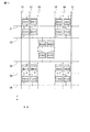
図10は、図9に示したカラーフィルタの配置例に対応するデータ線Sおよび走査線Gの一構成例を示す図である。
レッドカラーフィルタCFR、グリーンカラーフィルタCFG、ブルーカラーフィルタCFB、およびブラックカラーフィルタCFNのそれぞれに対向する電極として、主画素PX11は電極EA11、EB11、EC11、およびED11を備え、主画素PX31は電極EA31、EB31、EC31、およびED31を備え、主画素PX22は電極EA22、EB22、EC22、およびED22を備え、主画素PX13は電極EA13、EB13、EC13、およびED13を備え、主画素PX33は電極EA33、EB33、EC33、およびED33を備えている。
FIG. 10 is a diagram showing a configuration example of the data lines S and the scanning lines G corresponding to the arrangement example of the color filters shown in FIG.
The main pixel PX11 includes electrodes EA11, EB11, EC11, and ED11 as electrodes facing the red color filter CFR, the green color filter CFG, the blue color filter CFB, and the black color filter CFN, respectively, and the main pixel PX31 includes the electrode EA31. , EB31, EC31, and ED31, the main pixel PX22 includes electrodes EA22, EB22, EC22, and ED22, the main pixel PX13 includes electrodes EA13, EB13, EC13, and ED13, and the main pixel PX33 includes electrodes EA33, EB33. , EC33, and ED33.
電極EA11、ED11、EA13、およびED13は、データ線S1によってデータ信号を供給される。電極EB11、EC11、EB13、およびEC13は、データ線S2によってデータ信号を供給される。電極EA22およびED22は、データ線S3によってデータ信号を供給される。電極EB22およびEC22は、データ線S4によってデータ信号を供給される。電極EA31、ED31、EA33、およびED33は、データ線S5によってデータ信号を供給される。電極EB31、EC31、EB33、およびEC33は、データ線S6によってデータ信号を供給される。 The electrodes EA11, ED11, EA13, and ED13 are supplied with a data signal by the data line S1. The electrodes EB11, EC11, EB13, and EC13 are supplied with a data signal by the data line S2. The electrodes EA22 and ED22 are supplied with a data signal by the data line S3. The electrodes EB22 and EC22 are supplied with a data signal by the data line S4. The electrodes EA31, ED31, EA33, and ED33 are supplied with a data signal by the data line S5. The electrodes EB31, EC31, EB33, and EC33 are supplied with a data signal by the data line S6.
電極EA11、EB11、EA31、およびEB31は、走査線G1によって駆動を制御される。電極ED11、EC11、ED31、およびEC31は、走査線G2によって駆動を制御される。電極EA22およびEB22は、走査線G3によって駆動を制御される。電極ED22およびEC22は、走査線G4によって駆動を制御される。電極EA13、EB13、EA33、およびEB33は、走査線G5によって駆動を制御される。電極ED13、EC13、ED33、およびEC33は、走査線G6によって駆動を制御される。 The driving of the electrodes EA11, EB11, EA31, and EB31 is controlled by the scanning line G1. The driving of the electrodes ED11, EC11, ED31, and EC31 is controlled by the scanning line G2. The driving of the electrodes EA22 and EB22 is controlled by the scanning line G3. The driving of the electrodes ED22 and EC22 is controlled by the scanning line G4. The driving of the electrodes EA13, EB13, EA33, and EB33 is controlled by the scanning line G5. The driving of the electrodes ED13, EC13, ED33, and EC33 is controlled by the scanning line G6.
図11は、図9に示したカラーフィルタの配置例に対応するデータ線Sおよび走査線Gの他の構成例を示す図である。
本構成例は、データ線S4および走査線G3が配置されていない点で、図10に示した構成例と相違している。図示した例では、電極ED11、EA11、EB11、ED31、EA31、及びEB31は、走査線G1によって駆動を制御される。電極EC11、EA22、EB22、及びEC31は、走査線G2によって駆動を制御される。電極ED22及びEC22は、走査線G4によって駆動を制御される。電極ED13、EA13、EB13、ED33、EA33、及びEB33は、走査線G5によって駆動を制御される。電極EC13及びEC33は、走査線G6によって駆動を制御される。また、電極ED11及びED13は、データ線S1によってデータ信号を供給される。電極EA11、EC11、EA13、及びEC13は、データ線S2によってデータ信号を供給される。電極EB11、EA22、ED22、及びEB13は、データ線S3によってデータ信号を供給される。電極ED31、EB22、EC22及びED33は、データ線S5によってデータ信号を供給される。電極EA31、EC31、EA33、及びEC33は、データ線S6によってデータ信号を供給される。電極EB31及びEB33は、データ線S7によってデータ信号を供給される。
本構成例によれば、データ線Sの本数、および走査線Gの本数を削減することができ、表示パネルPNLの透過率を向上させることができる。
FIG. 11 is a diagram showing another configuration example of the data lines S and the scanning lines G corresponding to the arrangement example of the color filters shown in FIG.
This configuration example is different from the configuration example shown in FIG. 10 in that the data line S4 and the scanning line G3 are not arranged. In the illustrated example, driving of the electrodes ED11, EA11, EB11, ED31, EA31, and EB31 is controlled by the scanning line G1. The driving of the electrodes EC11, EA22, EB22, and EC31 is controlled by the scanning line G2. The driving of the electrodes ED22 and EC22 is controlled by the scanning line G4. The driving of the electrodes ED13, EA13, EB13, ED33, EA33, and EB33 is controlled by the scanning line G5. The driving of the electrodes EC13 and EC33 is controlled by the scanning line G6. The electrodes ED11 and ED13 are supplied with a data signal by the data line S1. The electrodes EA11, EC11, EA13, and EC13 are supplied with a data signal by the data line S2. The electrodes EB11, EA22, ED22, and EB13 are supplied with a data signal by the data line S3. The electrodes ED31, EB22, EC22 and ED33 are supplied with a data signal by the data line S5. The electrodes EA31, EC31, EA33, and EC33 are supplied with a data signal by the data line S6. The electrodes EB31 and EB33 are supplied with a data signal by the data line S7.
According to this configuration example, the number of data lines S and the number of scanning lines G can be reduced, and the transmittance of the display panel PNL can be improved.
図12は、図9に示したカラーフィルタの配置例に対応するデータ線Sおよび走査線Gの他の構成例を示す図である。
本構成例は、データ線S2、S4、S6が配置されていない点で、図10に示した構成例と相違している。図示した例では、電極EB11、EC11、EA22、ED22、EB13、およびEC13は、データ線S3によってデータ信号を供給される。電極EA31、ED31、EB22、EC22、EA33、およびED33は、データ線S5によってデータ信号を供給される。電極EB31、EC31、EB33、およびEC33は、データ線S7によってデータ信号を供給される。本構成例によれば、データ線Sの本数を削減することができる。
FIG. 12 is a diagram showing another configuration example of the data lines S and the scanning lines G corresponding to the arrangement example of the color filters shown in FIG.
This configuration example is different from the configuration example shown in FIG. 10 in that the data lines S2, S4, and S6 are not arranged. In the illustrated example, the electrodes EB11, EC11, EA22, ED22, EB13, and EC13 are supplied with a data signal by the data line S3. The electrodes EA31, ED31, EB22, EC22, EA33, and ED33 are supplied with a data signal by the data line S5. The electrodes EB31, EC31, EB33, and EC33 are supplied with a data signal by the data line S7. According to this configuration example, the number of data lines S can be reduced.
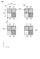
図13は、カラーフィルタの他の配置例を示す図である。
本配置例は、主画素PX22が省略され主画素PXがマトリクス状に配列されている点、およびブラックカラーフィルタCFNの一部がホワイトカラーフィルタCFWに置換されている点で、図9に示した配置例と相違している。ホワイトカラーフィルタCFWは、ドットパターンと右下がりの斜線パターンの組み合わせで示す領域である。
FIG. 13 is a diagram showing another arrangement example of the color filters.
This arrangement example is shown in FIG. 9 in that the main pixels PX22 are omitted and the main pixels PX are arranged in a matrix, and that part of the black color filter CFN is replaced with the white color filter CFW. This is different from the arrangement example. The white color filter CFW is an area indicated by a combination of a dot pattern and a diagonally downward-sloping pattern.
間隔W2は、特に限定されず、幅W1よりも小さくてもよい。また、間隔W4も、特に限定されず、幅W3よりも小さくてもよい。主画素PX11およびPX33は、図9に示した配置例と同様、レッドカラーフィルタCFR、グリーンカラーフィルタCFG、ブルーカラーフィルタCFB、およびブラックカラーフィルタCFNを備えている。主画素PX31およびPX13は、レッドカラーフィルタCFR、グリーンカラーフィルタCFG、およびブルーカラーフィルタCFBを備えており、ブラックカラーフィルタCFNに代わってホワイトカラーフィルタCFWを備えている。つまり、主画素PX11のブラックカラーフィルタCFN、主画素PX11のブルーカラーフィルタCFB、主画素PX31のホワイトカラーフィルタCFW、および主画素PX31のブルーカラーフィルタCFBが、この順に第1方向Xに並んでいる。また、主画素PX11のレッドカラーフィルタCFR、主画素PX11のブラックカラーフィルタCFN、主画素PX13のレッドカラーフィルタCFR、および主画素PX13のホワイトカラーフィルタCFWが、この順に第2方向Yに並んでいる。 The interval W2 is not particularly limited and may be smaller than the width W1. The interval W4 is also not particularly limited and may be smaller than the width W3. The main pixels PX11 and PX33 include a red color filter CFR, a green color filter CFG, a blue color filter CFB, and a black color filter CFN, as in the arrangement example shown in FIG. The main pixels PX31 and PX13 include a red color filter CFR, a green color filter CFG, and a blue color filter CFB, and include a white color filter CFW instead of the black color filter CFN. That is, the black color filter CFN of the main pixel PX11, the blue color filter CFB of the main pixel PX11, the white color filter CFW of the main pixel PX31, and the blue color filter CFB of the main pixel PX31 are arranged in this order in the first direction X. .. The red color filter CFR of the main pixel PX11, the black color filter CFN of the main pixel PX11, the red color filter CFR of the main pixel PX13, and the white color filter CFW of the main pixel PX13 are arranged in this order in the second direction Y. ..
ブラックカラーフィルタCFNを備えた主画素PXと、ホワイトカラーフィルタCFWを備えた主画素PXとは、図示した例では、数の比率が1:1となる様に配置されているが、これに限定されるものではなく、ブラックカラーフィルタCFNを備えた主画素PXが、ホワイトカラーフィルタCFWを備えた主画素PXよりも多くてもよい。逆に、ホワイトカラーフィルタCFWを備えた主画素PXが、ブラックカラーフィルタCFNを備えた主画素PXよりも多くてもよい。また、ブラックカラーフィルタCFNを備えた主画素PXと、ホワイトカラーフィルタCFWを備えた主画素PXとは、図示した例では第1方向Xおよび第2方向Yに交互に並んでいるが、これに限定されるものではなく、例えば、第1方向Xには交互に並び、第2方向Yにそれぞれ同じ構成の主画素PX同士で並んでいてもよい。 In the illustrated example, the main pixel PX having the black color filter CFN and the main pixel PX having the white color filter CFW are arranged so that the ratio of the numbers is 1:1, but the present invention is not limited to this. However, the number of main pixels PX having the black color filter CFN may be larger than the number of main pixels PX having the white color filter CFW. On the contrary, the number of main pixels PX having the white color filter CFW may be larger than the number of main pixels PX having the black color filter CFN. The main pixel PX having the black color filter CFN and the main pixel PX having the white color filter CFW are alternately arranged in the first direction X and the second direction Y in the illustrated example. For example, the main pixels PX may be alternately arranged in the first direction X and may be arranged in the second direction Y with the main pixels PX having the same configuration.
なお、ブラックカラーフィルタCFNは、図示した例では、ホワイトカラーフィルタCFWに代わって配置されているが、レッドカラーフィルタCFR、グリーンカラーフィルタCFG、およびブルーカラーフィルタCFBのうちいずれかに代わって配置されていてもよい。つまり、画素PXは、レッドカラーフィルタCFR、グリーンカラーフィルタCFG、およびブルーカラーフィルタCFBのうちいずれか2つを備え、且つ、ホワイトカラーフィルタCFWおよびブラックカラーフィルタCFNを備えていてもよい。 Although the black color filter CFN is arranged in place of the white color filter CFW in the illustrated example, it is arranged in place of any of the red color filter CFR, the green color filter CFG, and the blue color filter CFB. May be. That is, the pixel PX may include any two of the red color filter CFR, the green color filter CFG, and the blue color filter CFB, and may include the white color filter CFW and the black color filter CFN.
本変形例によれば、複数の主画素PXのうちいくつかは、N画素ではなくW画素を備えている。このため、表示装置DSPは、表示パネルPNLの透過率を向上させることができ、また、主面PNLaに表示される画像の輝度を向上させることができる。 According to this modification, some of the plurality of main pixels PX include W pixels instead of N pixels. Therefore, the display device DSP can improve the transmittance of the display panel PNL and also can improve the brightness of the image displayed on the main surface PNLa.
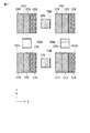
図14は、カラーフィルタの他の配置例を示す図である。
図示した配置例は、主画素PX22が省略され主画素PXがマトリクス状に配列されている点、および主画素PXのブラックカラーフィルタCFNが全てホワイトカラーフィルタCFWに置換されている点で、図9に示した配置例と相違している。ブラックカラーフィルタCFNは、主画素PXの間に位置している。
FIG. 14 is a diagram showing another arrangement example of the color filters.
The arrangement example shown in FIG. 9 is that the main pixels PX22 are omitted and the main pixels PX are arranged in a matrix, and that the black color filters CFN of the main pixels PX are all replaced with the white color filters CFW. This is different from the arrangement example shown in. The black color filter CFN is located between the main pixels PX.
主画素PX11、PX31、PX13、PX33は、それぞれ、レッドカラーフィルタCFR、グリーンカラーフィルタCFG、ブルーカラーフィルタCFBを備え、ブラックカラーフィルタCFNに代わってホワイトカラーフィルタCFWを備えている。主画素PX11と主画素PX31との間には、ブラックカラーフィルタCFNが配置されたダミー画素PDMが形成されている。同様に、主画素PX13と主画素PX33との間、主画素PX11と主画素PX13との間、および、主画素PX31と主画素PX33との間に、ダミー画素PDMが形成されている。表示パネルPNLの透過率を向上させる観点から、主画素PXとダミー画素PDMとは、互いに離間していることが望ましく、主画素PXのカラーフィルタとブラックカラーフィルタCFNとの間の領域には、カラーフィルタが配置されていないことが望ましい。なお、ブラックカラーフィルタCFNは、第1方向Xまたは第2方向Yにおける主画素PXの間に配置されるものと限定されるものではなく、例えば、第1方向Xおよび第2方向Yと交差する方向において、主画素PX11と主画素PX33との間に配置されてもよい。 Each of the main pixels PX11, PX31, PX13, PX33 includes a red color filter CFR, a green color filter CFG, a blue color filter CFB, and a white color filter CFW in place of the black color filter CFN. A dummy pixel PDM in which a black color filter CFN is arranged is formed between the main pixel PX11 and the main pixel PX31. Similarly, dummy pixels PDM are formed between the main pixels PX13 and PX33, between the main pixels PX11 and PX13, and between the main pixels PX31 and PX33. From the viewpoint of improving the transmittance of the display panel PNL, it is desirable that the main pixel PX and the dummy pixel PDM are separated from each other, and a region between the color filter of the main pixel PX and the black color filter CFN is It is desirable that no color filter is arranged. The black color filter CFN is not limited to being arranged between the main pixels PX in the first direction X or the second direction Y, and intersects the first direction X and the second direction Y, for example. It may be arranged between the main pixel PX11 and the main pixel PX33 in the direction.
表示パネルPNLの光透過率の低下を抑制する観点から、ブラックカラーフィルタCFNの面積は、1つの主画素PXに含まれるレッドカラーフィルタCFR、グリーンカラーフィルタCFG、ブルーカラーフィルタCFB、およびホワイトカラーフィルタCFWの面積の和よりも小さいことが望ましい。つまり、ダミー画素PDMは、主画素PXよりも小さいことが望ましい。また、主面PNLbに表示される反転画像の視認性を充分に低下させる観点から、ブラックカラーフィルタCFNの面積は、1つの主画素PXに含まれるレッドカラーフィルタCFR、グリーンカラーフィルタCFG、ブルーカラーフィルタCFB、およびホワイトカラーフィルタCFWのうち最小のものの面積と同等以上であることが望ましい。 From the viewpoint of suppressing the reduction of the light transmittance of the display panel PNL, the area of the black color filter CFN is the red color filter CFR, the green color filter CFG, the blue color filter CFB, and the white color filter included in one main pixel PX. It is desirable that it is smaller than the sum of the areas of CFW. That is, it is desirable that the dummy pixel PDM is smaller than the main pixel PX. Further, from the viewpoint of sufficiently reducing the visibility of the inverted image displayed on the main surface PNLb, the area of the black color filter CFN is the red color filter CFR, the green color filter CFG, and the blue color filter included in one main pixel PX. It is desirable that the area is equal to or larger than the area of the smallest one of the filter CFB and the white color filter CFW.
従って、ダミー画素PDMの第2方向Yの幅W8は、幅W1よりも小さく、間隔W2よりも小さいことが望ましい。ダミー画素PDMの第1方向Xの幅W9は、幅W3よりも小さく、間隔W4よりも小さいことが望ましい。ブラックカラーフィルタCFNと、主画素PXのカラーフィルタとが、第2方向YにおいてピッチPT5で隣り合い、第1方向XにおいてピッチPT6で隣り合っているとする。このとき、ピッチPT5はピッチPT1よりも大きく、ピッチPT6はピッチPT3よりも大きいことが望ましい。 Therefore, the width W8 of the dummy pixel PDM in the second direction Y is preferably smaller than the width W1 and smaller than the interval W2. The width W9 of the dummy pixel PDM in the first direction X is preferably smaller than the width W3 and smaller than the interval W4. It is assumed that the black color filter CFN and the color filter of the main pixel PX are adjacent to each other at the pitch PT5 in the second direction Y and at the pitch PT6 in the first direction X. At this time, it is desirable that the pitch PT5 is larger than the pitch PT1 and the pitch PT6 is larger than the pitch PT3.
この様な配置例においても、上記したのと同様の効果を得ることができる。 Even in such an arrangement example, the same effect as described above can be obtained.
図15は、主画素PX中のカラーフィルタの構成例を示した図である。
上記のカラーフィルタの配置例において、主画素PX中のカラーフィルタの構成は、特に限定されるものではなく、本図に示したストライプ状の配置であってもよい。
FIG. 15 is a diagram showing a configuration example of the color filter in the main pixel PX.
In the arrangement example of the color filters described above, the configuration of the color filters in the main pixel PX is not particularly limited, and may be the stripe arrangement shown in this figure.
図示した例において、レッドカラーフィルタCFR、グリーンカラーフィルタCFG、ブルーカラーフィルタCFBは、第2方向Yにストライプ状に延在し、第1方向Xに並んでいる。ブラックカラーフィルタCFNまたはホワイトカラーフィルタCFWも、第2方向Yにストライプ状に延在し、レッドカラーフィルタCFR、グリーンカラーフィルタCFG、ブルーカラーフィルタCFBのいずれかと第1方向Xで隣り合っている。
上記の構成のカラーフィルタを有する主画素PXは、例えば、図9、図13、および図14に示した配置例に適用可能である。以上の配置例は、主画素PXに4つのカラーフィルタが配置されている場合の配置例であるが、主画素PXに3つのカラーフィルタが配置されている場合であっても、上記と同様の効果を得ることができる。次に、主画素PXが3つのカラーフィルタで構成される場合の配置例について説明する。
In the illustrated example, the red color filter CFR, the green color filter CFG, and the blue color filter CFB extend in a stripe shape in the second direction Y and are arranged in the first direction X. The black color filter CFN or the white color filter CFW also extends in a stripe shape in the second direction Y and is adjacent to any one of the red color filter CFR, the green color filter CFG, and the blue color filter CFB in the first direction X.
The main pixel PX having the color filter configured as described above can be applied to the arrangement examples shown in FIGS. 9, 13, and 14, for example. The above arrangement example is an arrangement example in the case where four color filters are arranged in the main pixel PX, but even when three color filters are arranged in the main pixel PX, the same as above. The effect can be obtained. Next, an arrangement example when the main pixel PX is composed of three color filters will be described.
図16は、カラーフィルタの他の配置例を示す図である。
図示した配置例は、主画素PXがマトリクス状に配列されている点と、それぞれの主画素PXにレッドカラーフィルタCFR、グリーンカラーフィルタCFG、ブルーカラーフィルタCFB、およびブラックカラーフィルタCFNのうちいずれか3つがストライプ状に配置されている点と、で図9に示した配置例と相違している。
FIG. 16 is a diagram showing another arrangement example of the color filters.
In the illustrated arrangement example, the main pixels PX are arranged in a matrix, and each of the main pixels PX has one of a red color filter CFR, a green color filter CFG, a blue color filter CFB, and a black color filter CFN. The difference from the arrangement example shown in FIG. 9 is that three pieces are arranged in a stripe shape.
主画素PX11、PX31、およびPX51は、この順に第1方向Xに間隔を空けて並んでいる。同様に、主画素PX13、PX33,およびPX53は、この順に第1方向Xに間隔を空けて並び、主画素PX15、PX35、およびPX55は、この順に第1方向Xに間隔を空けて並んでいる。主画素PX11、PX13、およびPX15は、この順に第2方向Yに間隔を空けて並んでいる。同様に、主画素PX31、PX33、およびPX35は、この順に第2方向Yに間隔を空けて並び、主画素PX51、PX53、およびPX55は、この順に第2方向Yに間隔を空けて並んでいる。 The main pixels PX11, PX31, and PX51 are arranged in this order at intervals in the first direction X. Similarly, the main pixels PX13, PX33, and PX53 are arranged in this order at intervals in the first direction X, and the main pixels PX15, PX35, and PX55 are arranged in this order at intervals in the first direction X. .. The main pixels PX11, PX13, and PX15 are arranged in this order at intervals in the second direction Y. Similarly, the main pixels PX31, PX33, and PX35 are arranged in this order at intervals in the second direction Y, and the main pixels PX51, PX53, and PX55 are arranged in this order at intervals in the second direction Y. ..
主画素PX11には、ブラックカラーフィルタCFN、グリーンカラーフィルタCFG、およびブルーカラーフィルタCFBが、この順に第1方向Xに並んで配置されている。主画素PX31には、レッドカラーフィルタCFR、ブラックカラーフィルタCFN、およびブルーカラーフィルタCFBが、この順に第1方向Xに並んで配置されている。主画素PX51には、レッドカラーフィルタCFR、グリーンカラーフィルタCFG、およびブラックカラーフィルタCFNが、この順に第1方向Xに並んで配置されている。主画素PX13およびPX55は、主画素PX31と同様の構成を取っている。主画素PX33およびPX15は、主画素PX51と同様の構成を取っている。主画素PX53およびPX35は、主画素PX11と同様の構成を取っている。 In the main pixel PX11, a black color filter CFN, a green color filter CFG, and a blue color filter CFB are arranged side by side in this order in the first direction X. In the main pixel PX31, a red color filter CFR, a black color filter CFN, and a blue color filter CFB are arranged side by side in this order in the first direction X. In the main pixel PX51, a red color filter CFR, a green color filter CFG, and a black color filter CFN are arranged side by side in this order in the first direction X. The main pixels PX13 and PX55 have the same configuration as the main pixel PX31. The main pixels PX33 and PX15 have the same configuration as the main pixel PX51. The main pixels PX53 and PX35 have the same configuration as the main pixel PX11.
つまり、図示した例では、主画素PXは、レッドカラーフィルタCFR、グリーンカラーフィルタCFG、およびブルーカラーフィルタCFBのうち、いずれか1つがブラックカラーフィルタCFNに置き換えられている。レッドカラーフィルタCFRが置き換えられた主画素PXの隣には、グリーンカラーフィルタCFGまたはブルーカラーフィルタCFBが置き換えられた主画素PXが配置されている。 That is, in the illustrated example, in the main pixel PX, any one of the red color filter CFR, the green color filter CFG, and the blue color filter CFB is replaced with the black color filter CFN. Next to the main pixel PX in which the red color filter CFR is replaced, the main pixel PX in which the green color filter CFG or the blue color filter CFB is replaced is arranged.
図17は、カラーフィルタの他の配置例を示す図である。
図示した配置例は、以下の3点で、図9に示した配置例と相違している。1点目は、主画素PXがマトリクス状に配列されていることである。2点目は、主画素PXにレッドカラーフィルタCFR、グリーンカラーフィルタCFG、およびブルーカラーフィルタCFB、がストライプ状に配置されていることである。3点目は、主画素PXの間にダミー画素PDMが配置されていることである。
FIG. 17 is a diagram showing another arrangement example of the color filters.
The illustrated arrangement example differs from the arrangement example shown in FIG. 9 in the following three points. The first point is that the main pixels PX are arranged in a matrix. The second point is that the red color filter CFR, the green color filter CFG, and the blue color filter CFB are arranged in stripes in the main pixel PX. The third point is that dummy pixels PDM are arranged between the main pixels PX.
それぞれの主画素PXにおいて、レッドカラーフィルタCFR、グリーンカラーフィルタCFG、およびブルーカラーフィルタCFBは、第2方向Yに延在し、この順に第1方向Xに並んでいる。ブラックカラーフィルタCFNの配置位置や大きさなどは、図14に示した配置例と同様である。 In each main pixel PX, the red color filter CFR, the green color filter CFG, and the blue color filter CFB extend in the second direction Y, and are arranged in this order in the first direction X. The arrangement position and size of the black color filter CFN are the same as those in the arrangement example shown in FIG.
本実施形態において、表示装置DSPは、外光Loutおよび照明光Linの両方を利用可能なため、表示モードを適宜切り替えることで、照明光Linの利用効率を向上させることができる。表示モードは、例えば、光源ユニットLUの駆動方法や、主画素PXの表示方法に相当する。次に、表示モードを切り替えるためのシステム、および各表示モードの一例を説明する。 In the present embodiment, the display device DSP can use both the external light Lout and the illumination light Lin, so that the use efficiency of the illumination light Lin can be improved by appropriately switching the display mode. The display mode corresponds to, for example, the driving method of the light source unit LU or the display method of the main pixel PX. Next, a system for switching the display mode and an example of each display mode will be described.
図18は、表示装置DSPの表示モードの切り替えを制御する際のデータの流れを示すブロック図である。
表示装置DSPは、さらに、ホストコンピュータHOST、外光センサSNS、セレクタSLC、および制御部100を備えている。
FIG. 18 is a block diagram showing the flow of data when controlling the switching of the display mode of the display device DSP.
The display device DSP further includes a host computer HOST, an external light sensor SNS, a selector SLC, and a
ホストコンピュータHOSTは、画像データを制御部100へ送信する。外光センサSNSは、外光Loutの輝度および色を検出する光センサであり、取得した環境データを制御部100へ送信する。外光センサSNSは、例えば、外光Loutのスペクトルを測定するスペクトルメータ、または外光Loutの赤成分、緑成分、および青成分を個別に測定するRGB輝度センサを備えている。RGB輝度センサは、例えば、レッドカラーフィルタを透過した外光Loutの輝度を測定するレッドセンサと、グリーンカラーフィルタを透過した外光Loutの輝度を測定するグリーンセンサと、ブルーカラーフィルタを透過した外光Loutの輝度を測定するブルーセンサと、を備えている。セレクタSLCは、観察者などにより任意に表示モードを選択するための選択データを切り替え可能なスイッチに相当し、入力された選択データを制御部100へ送信する。
The host computer HOST sends the image data to the
制御部100は、ホストコンピュータHOSTから入力された画像データ(RGBデータ)に、変換や補正などの信号処理を行う。このとき制御部100は、例えば、主画素PXにおける表現色のRGB比を表すリニアなRGBデータを、R画素、G画素およびB画素の輝度を表す階調データへ変換する。制御部100は、例えば、外光センサSNSから入力される環境データに応じて表示モードを切り替えてもよい。または、制御部100は、セレクタSLCから入力される選択データに応じて表示モードを切り替えてもよい。各表示モードに応じて処理された画像データは、制御部100から駆動部DRおよび光源ユニットLUへ送信される。
The
制御部100は、光源ユニットLUにおける消費電力を低減するために信号処理を行ってもよく、例えば、各主画素PXにおける散乱強度のデータを伸長する信号処理を行い駆動部DRへ送信し、散乱強度の伸長分だけ光源ユニットLUの輝度のデータを減縮する信号処理を行い光源ユニットLUへ送信する。また、主画素PXがW画素を備えている場合、制御部100は、RGBデータから階調データへの変換の際に、RGBデータのうち共通部分をW画素の輝度を表すWデータに割り付ける信号処理を行い、Wデータに割り付けられた分だけ減縮したRGBデータを、比率を維持したまま伸長する信号処理を行う。これにより、表示装置DSPは、主画素PXの輝度を向上させることができる。
The
制御部100は、環境データに応じて表示画像の色温度を調整してもよい。例えば、外光センサSNSによって測定された外光Loutが黄色味を帯びている場合、外光Loutが白色光である場合と同様に表示装置DSPが駆動すると、主画素PXの表現色が黄色味を帯びてしまう。この様な場合に、RGBデータにB画素の輝度を上昇させる色補正を行うことで、主画素PXを本来の色で表現することができる。
The
図19は、表示装置DSPの表示モードの一例を示す図である。
図示した表は、外光Loutの輝度の強さによって切り替えられる第1乃至第3表示モードを表している。この表において、Mode1は第1表示モードを指し示し、Mode2は第2表示モードを指し示し、Mode3は第3表示モードを指し示す。また、Highは外光Loutが強い状況を指し示し、Lowは外光Loutが弱い状況を指し示し、0は外光Loutが非常に弱いか、または外光Loutが存在しない状況を指し示す。また、OFFは光源ユニットLUの消灯を指し示し、ONは光源ユニットLUの点灯を指し示する。
FIG. 19 is a diagram showing an example of the display mode of the display device DSP.
The illustrated table shows the first to third display modes that are switched depending on the intensity of the brightness of the external light Lout. In this table, Mode1 indicates the first display mode, Mode2 indicates the second display mode, and Mode3 indicates the third display mode. High indicates a situation where the outside light Lout is strong, Low indicates a situation where the outside light Lout is weak, and 0 indicates a situation where the outside light Lout is very weak or there is no outside light Lout. Further, OFF indicates turning off the light source unit LU, and ON indicates turning on the light source unit LU.
外光LoutがHighの時、表示装置DSPは第1表示モードを選択する。すなわち、光源ユニットLUを全消灯し、外光Loutのみを利用して画像を表示する。外光LoutがLowの時、表示装置DSPは、第2表示モードを選択する。すなわち、光源ユニットLUを点灯し、外光Loutおよび照明光Linの両方を利用して画像を表示する。なお、このとき、光源ユニットLUは、R光源、G光源、およびB光源を全点灯し、白色光源として機能する。外光Loutが0の時、表示装置DSPは、第3表示モードを選択する。すなわち、光源ユニットLUは、R光源、G光源、およびB光源を逐次点灯する、いわゆるフィールドシーケンシャル(FCS)方式によって、照明光Linのみを利用して画像を表示する。なお、各表示モードにおける光源ユニットLUの点灯方法は、これに限定されるものではなく、例えば外光LoutがLowの時に第3表示モードが選択されて光源ユニットLUが逐次点灯してもよく、また、外光Loutが0の時に第2表示モードが選択されて光源ユニットLUが全点灯してもよい。 When the external light Lout is High, the display device DSP selects the first display mode. That is, all the light source units LU are turned off, and an image is displayed using only the external light Lout. When the external light Lout is Low, the display device DSP selects the second display mode. That is, the light source unit LU is turned on and an image is displayed using both the external light Lout and the illumination light Lin. At this time, the light source unit LU functions as a white light source by turning on all of the R light source, the G light source, and the B light source. When the external light Lout is 0, the display device DSP selects the third display mode. That is, the light source unit LU displays an image using only the illumination light Lin by a so-called field sequential (FCS) method in which the R light source, the G light source, and the B light source are sequentially turned on. The method of lighting the light source unit LU in each display mode is not limited to this. For example, when the external light Lout is Low, the third display mode may be selected and the light source unit LU may be sequentially lighted. Further, when the external light Lout is 0, the second display mode may be selected and all the light source units LU may be turned on.
図20は、図19に示した第2表示モードにおける表示装置DSPの挙動を説明する図である。
本図は、主面PNLaへの画像の表示に寄与している主画素PXを示している。
光変調層OMには、白色光LWの外光Loutおよび照明光Linが入射する。外光Loutおよび照明光Linは、レッドカラーフィルタCFRに対応する位置の光変調層OMで散乱され、レッドカラーフィルタCFRを透過して赤色光LRとして主面PNLaから出射される。同時に、散乱された外光Loutおよび照明光Linは、薄赤色光LWrとして主面PNLbから出射される。同様に、外光Loutおよび照明光Linは、グリーンカラーフィルタCFGに対応する位置の光変調層OMで散乱され、緑色光LGとして主面PNLaから出射され、薄緑色光LWgとして主面PNLbから出射される。また、外光Loutおよび照明光Linは、ブルーカラーフィルタCFBに対応する位置の光変調層OMで散乱され、青色光LBとして主面PNLaから出射され、薄青色光LWbとして主面PNLbから出射される。
ブラックカラーフィルタCFNに対応する位置の光変調層OMで散乱された外光Loutおよび照明光Linは、白色光LWとして主面PNLbから出射され、主面PNLaからは出射されない。
FIG. 20 is a diagram for explaining the behavior of the display device DSP in the second display mode shown in FIG.
This figure shows the main pixels PX that contribute to the display of an image on the main surface PNLa.
The external light Lout of the white light LW and the illumination light Lin are incident on the light modulation layer OM. The external light Lout and the illumination light Lin are scattered by the light modulation layer OM at a position corresponding to the red color filter CFR, pass through the red color filter CFR, and are emitted from the main surface PNLa as red light LR. At the same time, the scattered external light Lout and the illumination light Lin are emitted from the main surface PNLb as light red light LWr. Similarly, the external light Lout and the illumination light Lin are scattered by the light modulation layer OM at a position corresponding to the green color filter CFG, emitted as green light LG from the main surface PNLa, and emitted as light green light LWg from the main surface PNLb. To be done. The external light Lout and the illumination light Lin are scattered by the light modulation layer OM at a position corresponding to the blue color filter CFB, emitted as blue light LB from the main surface PNLa, and emitted as light blue light LWb from the main surface PNLb. It
The external light Lout and the illumination light Lin scattered by the light modulation layer OM at the position corresponding to the black color filter CFN are emitted from the main surface PNLb as white light LW, and are not emitted from the main surface PNLa.
図21は、図19に示した第2表示モードにおける表示装置DSPの挙動を説明する図である。
本図は、主面PNLaへの画像の表示に寄与していない主画素PXを示している。
ブラックカラーフィルタCFNに対応する位置においては、図20に示した場合と同様に、光変調層OMが散乱モードとなってもよい。これにより、外光Loutおよび照明光Linは、白色光LWとして主面PNLbから出射される。
以上の様に、ダミー画素は、主画素PXの表示状態に関係なく、主面PNLbから白色光を出射することができる。
FIG. 21 is a diagram for explaining the behavior of the display device DSP in the second display mode shown in FIG.
This figure shows a main pixel PX that does not contribute to the display of an image on the main surface PNLa.
At the position corresponding to the black color filter CFN, the light modulation layer OM may be in the scattering mode as in the case shown in FIG. As a result, the external light Lout and the illumination light Lin are emitted from the main surface PNLb as white light LW.
As described above, the dummy pixel can emit white light from the main surface PNLb regardless of the display state of the main pixel PX.
図22は、図19に示した第3表示モードにおける表示装置DSPの挙動を説明する図である。
FCS方式では、1つの画像を表示する期間に相当する1フレームを、複数の期間(フィールド)に時間的に分割する。表示装置DSPは、各フィールドで異なる色の副画素を散乱モードとし、1フレーム中に表現された各フィールドの色が合成され、主画素PXの色として観察者に視認される。図示した例では、表示装置DSPは、1フレームを3つのフィールドに分割し、R画素が駆動されるレッド(R)フィールド、G画素が駆動されるグリーン(G)フィールド、および、B画素が駆動されるブルー(B)フィールドを、この順に逐次駆動している。なお、1フレームの開始時または終了時に、いずれの副画素も駆動されないブラック(B)フィールド、または全ての副画素が駆動されるホワイト(W)フィールドを挿入してもよい。RGBフィールドの前後でBまたはWフィールドを駆動することで、フレーム間での混色を抑制することができる。
22 is a diagram for explaining the behavior of the display device DSP in the third display mode shown in FIG.
In the FCS method, one frame corresponding to a period for displaying one image is temporally divided into a plurality of periods (fields). In the display device DSP, sub-pixels of different colors in each field are set to the scattering mode, and the colors of each field expressed in one frame are combined and visually recognized by the observer as the color of the main pixel PX. In the illustrated example, the display device DSP divides one frame into three fields, and a red (R) field in which R pixels are driven, a green (G) field in which G pixels are driven, and B pixels are driven. The blue (B) field is sequentially driven in this order. A black (B) field in which none of the subpixels are driven or a white (W) field in which all the subpixels are driven may be inserted at the start or end of one frame. By driving the B or W field before and after the RGB field, color mixing between frames can be suppressed.
次に、R、G、Bフィールドのそれぞれにおける駆動を説明する。
Rフィールドにおいて、光源ユニットLUは、赤色光LRの照明光Linを出射する。Rフィールドでは、レッドカラーフィルタCFRに対応する位置のR画素を散乱モードとなることで、照明光Linが主面PNLaおよびPNLbから赤色光LRとして出射される。また、ブラックカラーフィルタCFNに対応する位置のダミー画素も散乱モードとなってもよく、ダミー画素では照明光Linが主面PNLbのみから赤色光LRとして出射される。なお、ダミー画素における光変調層OMの散乱強度は、R画素における光変調層OMの散乱強度と異なっていてもよい。つまり、主面PNLbにおいて、ダミー画素から出射される赤色光LRの輝度は、R画素から出射される赤色光LRの輝度と異なっていてもよい。また、Rフィールドが主面PNLaへの画像の表示に寄与しない場合であっても、ダミー画素は散乱モードとすることができる。つまり、画像の表示に寄与しないRフィールドにおいて、主面PNLbから赤色光LRを出射することができる。
Next, driving in each of the R, G, and B fields will be described.
In the R field, the light source unit LU emits the illumination light Lin of the red light LR. In the R field, the R pixel at the position corresponding to the red color filter CFR is set to the scattering mode, so that the illumination light Lin is emitted as the red light LR from the principal surfaces PNLa and PNLb. Further, the dummy pixel at the position corresponding to the black color filter CFN may also be in the scattering mode, and the illumination light Lin is emitted as the red light LR only from the main surface PNLb in the dummy pixel. The scattering intensity of the light modulation layer OM in the dummy pixel may be different from the scattering intensity of the light modulation layer OM in the R pixel. That is, on the main surface PNLb, the brightness of the red light LR emitted from the dummy pixel may be different from the brightness of the red light LR emitted from the R pixel. Further, even when the R field does not contribute to the display of the image on the main surface PNLa, the dummy pixel can be set to the scattering mode. That is, the red light LR can be emitted from the main surface PNLb in the R field that does not contribute to the display of the image.
Gフィールドにおいても、Rフィールド同様、光源ユニットLUから緑色光LGの照明光Linを出射すると共に、グリーンカラーフィルタCFGに対応する位置のG画素と、ダミー画素とを散乱モードにすることができる。これにより、散乱された照明光Linは、主面PNLaおよびPNLbから緑色光LGとして出射される。Bフィールドにおいても、Rフィールド同様、光源ユニットLUから青色光LBの照明光Linを出射すると共に、ブルーカラーフィルタCFBに対応する位置のB画素と、ダミー画素とを散乱モードにすることができる。これにより、散乱された照明光Linは、主面PNLaおよびPNLbから青色光LBとして出射される。 Similarly to the R field, in the G field, the illumination light Lin of the green light LG can be emitted from the light source unit LU, and the G pixel at the position corresponding to the green color filter CFG and the dummy pixel can be set to the scattering mode. As a result, the scattered illumination light Lin is emitted as green light LG from the main surfaces PNLa and PNLb. Similarly to the R field, in the B field, the illumination light Lin of the blue light LB can be emitted from the light source unit LU, and the B pixel at the position corresponding to the blue color filter CFB and the dummy pixel can be set to the scattering mode. As a result, the scattered illumination light Lin is emitted as blue light LB from the principal surfaces PNLa and PNLb.
なお、1フレーム中にWフィールドが用意される場合、Wフィールドにおいて、光源ユニットLUは、R光源、G光源、およびB光源の全てを点灯し、白色光を出射する。そして、R画素、B画素、およびG画素を散乱モードとし、主面PNLaから白色光が出射する。このとき、ダミー画素が散乱モードと透過モードとのいずれであっても、主面PNLbから白色光が出射される。1フレーム中にBフィールドが用意される場合、Bフィールドにおいて、光源ユニットLUは消灯される。 When the W field is prepared in one frame, in the W field, the light source unit LU turns on all of the R light source, the G light source, and the B light source to emit white light. Then, the R pixel, the B pixel, and the G pixel are set to the scattering mode, and white light is emitted from the main surface PNLa. At this time, white light is emitted from the main surface PNLb regardless of whether the dummy pixel is in the scattering mode or the transmission mode. When the B field is prepared in one frame, the light source unit LU is turned off in the B field.
以上の様な第3表示モードによれば、散乱された照明光Linの、レッドカラーフィルタCFR、グリーンカラーフィルタCFG、およびブルーカラーフィルタCFBにおける吸収による損失を低減することができる。すなわち、光源ユニットLUの光の利用効率を向上させることが可能である。また、Rフィールドにおいては、R画素およびダミー画素に対応する領域でのみ照明光Linが散乱され、G画素およびB画素に対応する領域では照明光Linは消費されない。Gフィールド、およびBフィールドにおいても、同様に、照明光Linの消費を抑制することができるため、表示装置DSPは、照明光Linの側面PNLdにおける輝度の低下を抑制し、表示ムラを抑制することができる。 According to the third display mode as described above, it is possible to reduce the loss due to the absorption of the scattered illumination light Lin in the red color filter CFR, the green color filter CFG, and the blue color filter CFB. That is, it is possible to improve the light utilization efficiency of the light source unit LU. Further, in the R field, the illumination light Lin is scattered only in the regions corresponding to the R pixels and the dummy pixels, and the illumination light Lin is not consumed in the regions corresponding to the G pixels and the B pixels. Similarly, in the G field and the B field, since the consumption of the illumination light Lin can be suppressed, the display device DSP suppresses the decrease in the luminance of the side surface PNLd of the illumination light Lin and suppresses the display unevenness. You can
なお、主画素PXはW画素をさらに備えていてもよい。W画素は、各フィールドにおいて散乱モードとすることで、各フィールドの輝度を向上させることができる。また、W画素は、全てのフィールドにおいて散乱モードとすることで、1フレームで見た場合に白色光を表示するため、主画素PXの輝度を向上させることができる。 The main pixel PX may further include W pixels. By setting the W pixel in the scattering mode in each field, the brightness of each field can be improved. In addition, since the W pixel displays white light when viewed in one frame by setting the scattering mode in all fields, it is possible to improve the brightness of the main pixel PX.
図23は、図22で説明した第3表示モードの応用例を示す図である。
本図においては、Rフィールドのみを図示し、Gフィールド及びBフィールドを省略している。本表示方法においても、図19で図示したのと同様に、R、G、及びBフィールドを逐次駆動することで画像を表示する。図示した例では、表示装置DSPは、Rフィールドにおいて、G画素およびB画素を散乱モードとし、赤色光LRの照明光Linを散乱させている。主面PNLaに向かって散乱された照明光Linは、グリーンカラーフィルタCFGおよびブルーカラーフィルタCFBに吸収される。対して、主面PNLbに向かって散乱された照明光Linは、主面PNLbから出射される。同様に、GフィールドおよびBフィールドにおいても、主面PNLaから光を出射せずに、主面PNLbから光を出射することができる。つまり、この様な表示方法によれば、主画素PXは、主面PNLaと主面PNLbとで、異なる色を表示することができ、表示装置DSPは、例えば画像を主面PNLa側には表示せずに主面PNLb側にのみ表示することができる。
FIG. 23 is a diagram showing an application example of the third display mode described in FIG.
In this figure, only the R field is shown, and the G field and the B field are omitted. Also in this display method, similarly to the case shown in FIG. 19, an image is displayed by sequentially driving the R, G, and B fields. In the illustrated example, the display device DSP sets the G pixel and the B pixel in the scattering mode in the R field to scatter the illumination light Lin of the red light LR. The illumination light Lin scattered toward the main surface PNLa is absorbed by the green color filter CFG and the blue color filter CFB. On the other hand, the illumination light Lin scattered toward the main surface PNLb is emitted from the main surface PNLb. Similarly, in the G field and the B field, light can be emitted from the main surface PNLb without being emitted from the main surface PNLa. That is, according to such a display method, the main pixel PX can display different colors on the main surface PNLa and the main surface PNLb, and the display device DSP displays, for example, an image on the main surface PNLa side. Instead, it can be displayed only on the main surface PNLb side.
図24は、光源23からの出射光の色と、その出射光によって表示装置DSPが表現可能な色と、を示す表である。
表中の表現とは、各光源から出射された照明光Linが、レッドカラーフィルタCFR、グリーンカラーフィルタCFGおよびブルーカラーフィルタCFBを透過した後の色を示すものである。OFFとは、照明光Linが夫々のカラーフィルタを透過せずに黒表示となるケースを意味する。
FIG. 24 is a table showing colors of light emitted from the
The expression in the table indicates the color after the illumination light Lin emitted from each light source has passed through the red color filter CFR, the green color filter CFG, and the blue color filter CFB. “OFF” means a case where the illumination light Lin does not pass through the respective color filters and black display is performed.
FCS方式を利用する場合、光源ユニットLUは、レッドカラーフィルタCFR、グリーンカラーフィルタCFG、およびブルーカラーフィルタCFBを透過して、レッド、グリーン、およびブルーを表現できる光源の組み合わせであれば、R光源、G光源、およびB光源の組み合わせに限定されるものではない。光源ユニットLUは、3つの光源の組み合わせに限定されるものではなく、2つの光源の組み合わせであってもよい。
R光源、G光源、およびB光源は、それぞれレッド、グリーン、およびブルーを表現可能である。イエロー(Y)光を出射するY光源は、レッドおよびグリーンを表現可能である。マゼンタ(M)光を出射するM光源は、レッドおよびブルーを表現可能である。シアン(C)光を出射するC光源は、グリーンおよびブルーを表現可能である。従って、光源ユニットLUは、Y光源およびB光源の組み合わせ、M光源およびG光源の組み合わせ、またはC光源およびR光源の組み合わせであってもよい。また、光源ユニットLUは、Y光源およびM光源の組み合わせ、M光源およびC光源の組み合わせ、C光源およびY光源の組み合わせであってもよい。
When using the FCS method, the light source unit LU is a R light source if it is a combination of light sources that can express red, green, and blue through the red color filter CFR, the green color filter CFG, and the blue color filter CFB. It is not limited to the combination of the G light source, the G light source, and the B light source. The light source unit LU is not limited to the combination of three light sources, and may be a combination of two light sources.
The R light source, the G light source, and the B light source can represent red, green, and blue, respectively. The Y light source that emits yellow (Y) light can express red and green. The M light source that emits magenta (M) light can express red and blue. The C light source that emits cyan (C) light can express green and blue. Therefore, the light source unit LU may be a combination of Y light source and B light source, a combination of M light source and G light source, or a combination of C light source and R light source. Further, the light source unit LU may be a combination of Y light source and M light source, a combination of M light source and C light source, and a combination of C light source and Y light source.
なお、Y光源は、例えば、緑色光を出射するグリーンLEDと、緑色光を吸収し赤色光を発光するレッド蛍光体と、で構成される。M光源は、例えば、青色光を出射するブルーLEDと、青色光を吸収し赤色光を発光するレッド蛍光体と、で構成される。C光源は、例えば、青色光を出射するブルーLEDと、青色光を吸収し緑色光を発光するグリーン蛍光体と、で構成される。但し、Y光源は、グリーンLEDとレッドLEDとを同時に点灯させるものであってもよく、M光源は、ブルーLEDとレッドLEDとを同時に点灯させるものであってもよく、C光源は、ブルーLEDとグリーンLEDとを同時に点灯させるものであってもよい。 The Y light source includes, for example, a green LED that emits green light and a red phosphor that absorbs green light and emits red light. The M light source includes, for example, a blue LED that emits blue light and a red phosphor that absorbs blue light and emits red light. The C light source includes, for example, a blue LED that emits blue light and a green phosphor that absorbs blue light and emits green light. However, the Y light source may be one that simultaneously turns on the green LED and the red LED, the M light source may be one that simultaneously turns on the blue LED and the red LED, and the C light source may be the blue LED. And the green LED may be turned on at the same time.
図25は、散乱強度の補正を説明する図である。
表示領域DAにおいて、光源ユニットLUに近接する側である側面PNLcに近い位置では照明光Linの輝度は高く、光源ユニットLUから離間する側である側面PNLdに近い位置では照明光Linの輝度が低い。これは、前述の通り、照明光Linが光変調層OMでの散乱により消費されるためである。
FIG. 25 is a diagram for explaining the correction of the scattering intensity.
In the display area DA, the brightness of the illumination light Lin is high at a position close to the side surface PNLc that is close to the light source unit LU, and low at the position close to the side surface PNLd that is a side away from the light source unit LU. .. This is because the illumination light Lin is consumed by scattering in the light modulation layer OM as described above.
表示パネルPNLの斜線パターンの領域に画像が表示されるとする。図中のグラフの実線は、光変調層OMにおけるA−A’線に沿った照明光Linの輝度低下を示している。点Aは、表示領域DAの側面PNLcに近接する側の端部に位置し、点A’は、表示領域DAの側面PNLdに近接する側の端部に位置している。図中のグラフの点線は、斜線パターンの領域の輝度を均一化するために必要な、A−A’線に沿った光変調層OMの散乱強度の補正を示している。光変調層OMに電場を形成することで散乱モードとなる表示パネルPNLの場合、散乱強度の補正は、光変調層OMに電場を形成する電極への印加電圧の階調値を調節することで実施される。この階調値は、点Aに近い位置では最大値よりも低い値に設定され、点A’に近づくにつれて高くなる様に設定され、点A’において最大値に設定される。これにより、表示装置DSPは、側面PNLd近傍での輝度不足による表示ムラの発生を抑制することができる。 It is assumed that an image is displayed in the hatched pattern area of the display panel PNL. The solid line of the graph in the drawing indicates the decrease in the luminance of the illumination light Lin along the line A-A′ in the light modulation layer OM. The point A is located at the end of the display area DA on the side closer to the side surface PNLc, and the point A'is located on the end of the display area DA on the side closer to the side surface PNLd. The dotted line in the graph in the drawing shows the correction of the scattering intensity of the light modulation layer OM along the line A-A′, which is necessary to make the luminance of the hatched pattern region uniform. In the case of the display panel PNL which is in the scattering mode by forming an electric field in the light modulation layer OM, the scattering intensity is corrected by adjusting the gradation value of the voltage applied to the electrode forming the electric field in the light modulation layer OM. Be implemented. This gradation value is set to a value lower than the maximum value at a position close to the point A, set to be higher as it approaches the point A', and set to the maximum value at the point A'. Accordingly, the display device DSP can suppress the occurrence of display unevenness due to insufficient brightness near the side surface PNLd.
図26は、スキャン駆動を説明する図である。
表示領域DAの輝度の均一化は、スキャン駆動によっても実現可能である。スキャン駆動とは、表示領域DAを例えば第2方向Yに並ぶ複数のブロックに分割し、ブロック毎に逐次駆動を行う、というものである。
FIG. 26 is a diagram illustrating scan driving.
Uniformization of the brightness of the display area DA can also be realized by scan driving. The scan driving is to divide the display area DA into, for example, a plurality of blocks arranged in the second direction Y, and sequentially drive each block.
図示した例では、表示領域DAは、8つのブロックB1乃至B8に分割されている。ブロックB1乃至B8は、側面PNLdに近い位置から、この順に第2方向Yに並んでいる。なお、ブロックの数は、特に限定されるものではなく、7つ以下でも9つ以上でもよい。ブロック数を増加させれば表示ムラを抑制することができ、ブロック数を減少させれば表示装置DSPの駆動周波数を低減することができる。従って、表示装置DSPの設計等に応じて、好適なブロック数が適宜選択される。 In the illustrated example, the display area DA is divided into eight blocks B1 to B8. The blocks B1 to B8 are arranged in the second direction Y in this order from a position near the side surface PNLd. The number of blocks is not particularly limited, and may be 7 or less or 9 or more. If the number of blocks is increased, display unevenness can be suppressed, and if the number of blocks is decreased, the drive frequency of the display device DSP can be reduced. Therefore, a suitable number of blocks is appropriately selected according to the design of the display device DSP.
図示した例では、最初に、ブロックB1に配置された主画素PXのみが散乱モードとなり、ブロックB1に画像の一部が表示される。このとき、ブロックB2乃至B8に配置された主画素PXは透過モードであるため、照明光Linの輝度の低下を抑制しつつ、照明光LinをブロックB1へ導光することができる。次に、ブロックB2に配置された主画素PXのみが散乱モードとなり、ブロックB2に画像の一部が表示される。その後、ブロックB3乃至B8に配置された主画素PXが逐次散乱モードとなり、ブロックB3乃至B8に画像の一部が逐次表示される。ブロックB1乃至B8のそれぞれに表示された画像の一部が組み合わされて、1つの画像として観察者に視認される。 In the illustrated example, first, only the main pixels PX arranged in the block B1 are in the scattering mode, and a part of the image is displayed in the block B1. At this time, since the main pixels PX arranged in the blocks B2 to B8 are in the transmissive mode, the illumination light Lin can be guided to the block B1 while suppressing a decrease in the luminance of the illumination light Lin. Next, only the main pixels PX arranged in the block B2 enter the scattering mode, and a part of the image is displayed in the block B2. After that, the main pixels PX arranged in the blocks B3 to B8 enter the sequential scattering mode, and a part of the image is sequentially displayed in the blocks B3 to B8. A part of the images displayed in each of the blocks B1 to B8 are combined and viewed by the observer as one image.
スキャン駆動によれば、照明光Linの散乱による輝度低下は夫々のブロックB1乃至B8に対応する領域内でのみ生じるため、表示ムラの発生を抑制することができる。また、散乱強度の補正によって主画素PXの輝度を抑制する必要がないため、表示画像の輝度を向上させることができる。 According to the scan driving, the decrease in brightness due to the scattering of the illumination light Lin occurs only in the areas corresponding to the blocks B1 to B8, so that it is possible to suppress the occurrence of display unevenness. Further, since it is not necessary to suppress the brightness of the main pixel PX by correcting the scattering intensity, the brightness of the display image can be improved.
図27は、本実施形態に係る表示装置DSPの第1変形例を示す図である。
本変形例は、主画素PX11と主画素PX13との間の領域に電極EE12およびEH12を備えている点で、図3に図示した構成例と相違している。
FIG. 27 is a diagram showing a first modification of the display device DSP according to the present embodiment.
This modification example is different from the configuration example shown in FIG. 3 in that the electrodes EE12 and EH12 are provided in the region between the main pixel PX11 and the main pixel PX13.
主画素PX11と主画素PX13との間に、準画素QX12(QX)が形成されている。準画素QXは、主画素PXに準ずる構成を備えており、例えば、カラーフィルタFA乃至FDに代わって透明部材TPを備えている。透明部材TPは、例えば、白色光を透過させる無着色の樹脂によって形成されている。透明部材TPは、画像を表示していない時の表示パネルPNLの色味を調整するために、薄く着色されていてもよい。 A quasi pixel QX12 (QX) is formed between the main pixel PX11 and the main pixel PX13. The quasi pixel QX has a structure similar to that of the main pixel PX, and includes, for example, a transparent member TP instead of the color filters FA to FD. The transparent member TP is formed of, for example, an uncolored resin that transmits white light. The transparent member TP may be lightly colored in order to adjust the tint of the display panel PNL when an image is not displayed.
準画素QX12に対応する領域には、電極EE12、EH12および透明部材TP12が配置されている。電極EE12およびEH12は、電極ED11と電極EA13との間に位置し、互いに第2方向Yで隣り合っている。電極EE12は、第2方向で電極ED11と隣り合っており、電極EH12は、第2方向で電極EA13と隣り合っている。電極EE12およびEH12のそれぞれの大きさは、例えば電極EA13と同等であるが、電極EA13よりも大きくても小さくてもよい。
透明部材TP12は、カラーフィルタFD11とカラーフィルタFA13との間に位置し、電極EE12およびEH12と第3方向Zで対向している。透明部材TP12は、準画素QX12に対応する領域の全面に亘って配置されている。透明部材TP12は、第2方向YでカラーフィルタFD11およびFA13と接触している。透明部材TP12は、カラーフィルタFA13よりも面積が大きい。透明部材TP12の第2方向Yの幅W6は、カラーフィルタFA13の第2方向Yの幅W5よりも大きく、一例では、幅W6は幅W5の約2倍である。透明部材TP12は、例えば、オーバーコート層OCによって形成されている。
Electrodes EE12 and EH12 and a transparent member TP12 are arranged in a region corresponding to the quasi pixel QX12. The electrodes EE12 and EH12 are located between the electrode ED11 and the electrode EA13, and are adjacent to each other in the second direction Y. The electrode EE12 is adjacent to the electrode ED11 in the second direction, and the electrode EH12 is adjacent to the electrode EA13 in the second direction. The size of each of the electrodes EE12 and EH12 is, for example, equal to that of the electrode EA13, but may be larger or smaller than that of the electrode EA13.
The transparent member TP12 is located between the color filter FD11 and the color filter FA13, and faces the electrodes EE12 and EH12 in the third direction Z. The transparent member TP12 is arranged over the entire surface of the region corresponding to the quasi pixel QX12. The transparent member TP12 is in contact with the color filters FD11 and FA13 in the second direction Y. The transparent member TP12 has a larger area than the color filter FA13. The width W6 of the transparent member TP12 in the second direction Y is larger than the width W5 of the color filter FA13 in the second direction Y. In one example, the width W6 is about twice the width W5. The transparent member TP12 is formed of, for example, the overcoat layer OC.
準画素QX12は、電極EE12と共通電極CEとの間に生じる電場に応じて、光変調層OMの電極EE12と対向する領域の光散乱性を変調する。また、準画素QX12は、電極EH12と共通電極との間に生じる電場に応じて、光変調層OMの電場EH12と対向する領域の光散乱性を変調する。電極EE12およびEH12のそれぞれに対向する領域で散乱された光は、主面PNLaおよびPNLbから出射される。したがって、表示装置DSPは、表示パネルPNLの透明度を低下させることができ、外光が強い場合の画像の表示品位を向上させることができる。また、準画素QXをW画素として利用することで、画像の輝度を向上させることができる。 The quasi pixel QX12 modulates the light scattering property of a region of the light modulation layer OM facing the electrode EE12 according to an electric field generated between the electrode EE12 and the common electrode CE. Further, the quasi pixel QX12 modulates the light scattering property of the region of the light modulation layer OM facing the electric field EH12 according to the electric field generated between the electrode EH12 and the common electrode. The light scattered in the regions facing the electrodes EE12 and EH12 are emitted from the main surfaces PNLa and PNLb. Therefore, the display device DSP can reduce the transparency of the display panel PNL and can improve the display quality of an image when the external light is strong. Further, by using the quasi pixel QX as the W pixel, the brightness of the image can be improved.
図28は、図27に示した第1基板SUB1の構成例を示す図である。
図示した構成例は、準画素QXが配置されている点で、図10に図示した構成例と相違している。準画素QXは、主画素PXの間に配置されており、主画素PXおよび準画素QXは、第1方向Xおよび第2方向Yに交互に並んでいる。準画素QXは、画素電極EE、EF、EGおよびEHを備えている。
FIG. 28 is a diagram showing a configuration example of the first substrate SUB1 shown in FIG.
The illustrated configuration example is different from the configuration example illustrated in FIG. 10 in that the quasi pixel QX is arranged. The quasi-pixels QX are arranged between the main pixels PX, and the main pixels PX and the quasi-pixels QX are alternately arranged in the first direction X and the second direction Y. The quasi pixel QX includes pixel electrodes EE, EF, EG and EH.
準画素QX12の電極EF12および電極EG12は、電極EC11と電極EB13との間に位置している。電極EF12は、第1方向Xで電極EE12と隣り合い、第2方向Yで電極EC11と隣り合っている。電極EG12は、第1方向Xで電極EH12と隣り合い、第2方向Yで電極EF12およびEB13と隣り合っている。 The electrode EF12 and the electrode EG12 of the quasi pixel QX12 are located between the electrode EC11 and the electrode EB13. The electrode EF12 is adjacent to the electrode EE12 in the first direction X and adjacent to the electrode EC11 in the second direction Y. The electrode EG12 is adjacent to the electrode EH12 in the first direction X and is adjacent to the electrodes EF12 and EB13 in the second direction Y.
第1方向Xにおいて主画素PX11と主画素PX31との間に位置する準画素QX21は、電極EE21、EF21、EG21、およびEH21を備えている。電極EE21は、第1方向Xで電極EB11とEF21との間に位置し、電極EF21は、第1方向Xで電極EE21と電極EA31との間に位置している。電極EH21は、第1方向Xで電極EC11とEG21との間に位置し、電極EG21は、第1方向Xで電極EH21と電極ED31との間に位置している。 The quasi pixel QX21 located between the main pixel PX11 and the main pixel PX31 in the first direction X includes electrodes EE21, EF21, EG21, and EH21. The electrode EE21 is located between the electrodes EB11 and EF21 in the first direction X, and the electrode EF21 is located between the electrode EE21 and the electrode EA31 in the first direction X. The electrode EH21 is located between the electrodes EC11 and EG21 in the first direction X, and the electrode EG21 is located between the electrodes EH21 and ED31 in the first direction X.
電極EE12およびEH12は、データ線S1によってデータ信号を供給される。電極EF12およびEG12は、データ線S2によってデータ信号を供給される。電極EE21およびEH21は、データ線S3によってデータ信号を供給される。電極EF21およびEG21は、データ線S4によってデータ信号を供給される。電極EE21およびEF21は、走査線G1によって駆動を制御される。電極EG21およびEH21は、走査線G2によって駆動を制御される。電極EE12およびEF12は、走査線G3によって駆動を制御される。電極EG12およびEH32は、走査線G4によって駆動を制御される。 The electrodes EE12 and EH12 are supplied with a data signal by the data line S1. The electrodes EF12 and EG12 are supplied with a data signal by the data line S2. The electrodes EE21 and EH21 are supplied with a data signal by the data line S3. The electrodes EF21 and EG21 are supplied with a data signal by the data line S4. The driving of the electrodes EE21 and EF21 is controlled by the scanning line G1. The drive of the electrodes EG21 and EH21 is controlled by the scanning line G2. The driving of the electrodes EE12 and EF12 is controlled by the scanning line G3. The driving of the electrodes EG12 and EH32 is controlled by the scanning line G4.
第2方向Yにおいて主画素PX31と主画素PX33との間に位置する準画素QX32も、準画素QX12同様に、電極EE32、EF32、EG32、およびEH32を備えている。第1方向Xにおいて主画素PX13と主画素PX33との間に位置する準画素QX23も、準画素QX21同様に、電極EE23、EF23、EG23、およびEH23を備えている。 Similarly to the quasi pixel QX12, the quasi pixel QX32 located between the main pixel PX31 and the main pixel PX33 in the second direction Y also includes the electrodes EE32, EF32, EG32, and EH32. Similarly to the quasi pixel QX21, the quasi pixel QX23 located between the main pixel PX13 and the main pixel PX33 in the first direction X also includes electrodes EE23, EF23, EG23, and EH23.
なお、準画素QXは、主画素PXの間に配置されるのであれば、そのレイアウトは特に限定されるものではなく、例えば図13や図16に図示した配置例における主画素PXの間に配置されてもよい。また、準画素QXを図14や図17に示した配置例に加える場合、準画素QXは、その配置位置を主画素PX同士の間に限定されるものではなく、主画素PXとダミー画素PDMとの間や、ダミー画素PDM同士の間に配置されてもよい。 Note that the layout of the quasi-pixels QX is not particularly limited as long as it is arranged between the main pixels PX, and for example, the quasi-pixels QX are arranged between the main pixels PX in the arrangement examples shown in FIGS. 13 and 16. May be done. When the quasi pixel QX is added to the arrangement examples shown in FIGS. 14 and 17, the arrangement position of the quasi pixel QX is not limited to between the main pixels PX, but the main pixel PX and the dummy pixel PDM. , Or between the dummy pixels PDM.
図29は、本実施形態に係る表示装置DSPの第2変形例を示す図である。
本変形例は、準画素QXに対応する領域に電極EI12が配置されている点で、図27に図示した変形例と相違している。電極EI12は、透明部材TPの全面に亘って第3方向Xで対向し、電極ED11と電極EA13との間に配置されている。電極EI12は、第2方向Yで、電極ED11およびEA13と隣り合っている。
本変形例においても、第1変形例と同様の効果を得ることができる。
FIG. 29 is a diagram showing a second modification of the display device DSP according to the present embodiment.
This modification is different from the modification shown in FIG. 27 in that the electrode EI12 is arranged in the region corresponding to the quasi pixel QX. The electrode EI12 faces the entire surface of the transparent member TP in the third direction X and is arranged between the electrode ED11 and the electrode EA13. The electrode EI12 is adjacent to the electrodes ED11 and EA13 in the second direction Y.
Also in this modification, the same effect as that of the first modification can be obtained.
図30は、図29に示した第1基板SUB1の構成例を示す図である。
本構成例は、電極EI12、EI21、EI32、およびEI23が配置されている点で、図28に図示した構成例と相違している。
準画素QX12の電極EI12は、準画素QX12に対応する領域の全体に配置され、電極ED11と電極EA13との間だけではなく、電極EC11と電極EB13との間にも延在している。準画素QX21の電極EI21は、準画素QX21に対応する領域の全体に亘って配置され、電極EB11と電極EA31との間、および電極EC11と電極ED31との間に延在している。
電極EI12は、データ線S1によってデータ信号を供給され、走査線G4によって駆動を制御される。電極EI21は、データ線S3によってデータ信号を供給され、走査線G2によって駆動を制御される。
準画素QX32の電極EI32も、準画素QX12と同様に、電極EI32を備えている。準画素QX23の電極EI23も、準画素QX21と同様に、電極EI23を備えている。
FIG. 30 is a diagram showing a configuration example of the first substrate SUB1 shown in FIG.
This configuration example is different from the configuration example illustrated in FIG. 28 in that the electrodes EI12, EI21, EI32, and EI23 are arranged.
The electrode EI12 of the quasi pixel QX12 is arranged in the entire region corresponding to the quasi pixel QX12, and extends not only between the electrode ED11 and the electrode EA13 but also between the electrode EC11 and the electrode EB13. The electrode EI21 of the quasi pixel QX21 is arranged over the entire region corresponding to the quasi pixel QX21, and extends between the electrode EB11 and the electrode EA31 and between the electrode EC11 and the electrode ED31.
The electrode EI12 is supplied with a data signal by the data line S1 and its drive is controlled by the scanning line G4. The electrode EI21 is supplied with a data signal by the data line S3, and its drive is controlled by the scanning line G2.
The electrode EI32 of the quasi pixel QX32 is also provided with the electrode EI32 similarly to the quasi pixel QX12. The electrode EI23 of the quasi pixel QX23 also includes the electrode EI23, like the quasi pixel QX21.
図31は、本実施形態に係る表示装置DSPの第3変形例を示す図である。
図示した表示パネルPNLは、複数のコラム電極C(C1、C2、…、Cp)と、複数のロウ電極L(L1、L2、…、Lq)と、を備えた、いわゆるパッシブマトリクス型の表示パネルである。コラム電極Cは、第2方向Yに延在し第1方向Xに並んでいる。ロウ電極Lは、第1方向Xに延在し、第2方向Yに並んでいる。コラム電極Cは、第1ドライバDr1に電気的に接続され、ロウ電極Lは、第2ドライバDr2に電気的に接続されている。
コラム電極Cとロウ電極Lとが互いに交差して対向する領域が、副画素として動作する。例えば、コラム電極C1とロウ電極L1とが対向する領域が、副画素PA11に相当する。コラム電極C2とロウ電極L1とが対向する領域が、副画素PB11に相当する。コラム電極C2とロウ電極L2とが対向する領域が、副画素PC11に相当する。コラム電極C1とロウ電極L2とが対向する領域が、副画素PD11に相当する。
この様な変形例においても、上記したのと同様の効果を得ることができる。
FIG. 31 is a diagram showing a third modification of the display device DSP according to the present embodiment.
The illustrated display panel PNL includes a plurality of column electrodes C (C1, C2,..., Cp) and a plurality of row electrodes L (L1, L2,..., Lq), which is a so-called passive matrix display panel. Is. The column electrodes C extend in the second direction Y and are arranged in the first direction X. The row electrodes L extend in the first direction X and are arranged in the second direction Y. The column electrode C is electrically connected to the first driver Dr1, and the row electrode L is electrically connected to the second driver Dr2.
A region where the column electrode C and the row electrode L intersect and face each other operates as a subpixel. For example, the region where the column electrode C1 and the row electrode L1 face each other corresponds to the sub-pixel PA11. A region where the column electrode C2 and the row electrode L1 face each other corresponds to the sub-pixel PB11. The region where the column electrode C2 and the row electrode L2 face each other corresponds to the sub-pixel PC11. The region where the column electrode C1 and the row electrode L2 face each other corresponds to the sub-pixel PD11.
Even in such a modified example, the same effect as described above can be obtained.
次に、第2実施形態について説明する。第2実施形態に係る表示装置DSPは、ダミー画素が配置されていない点と、表示モードがFCS方式に限定される点と、で第1実施形態に係る表示装置DSPと相違している。 Next, a second embodiment will be described. The display device DSP according to the second embodiment differs from the display device DSP according to the first embodiment in that dummy pixels are not arranged and the display mode is limited to the FCS method.
図32は、第2実施形態に係る表示装置DSPの一構成例、およびその表示モードを示す図である。
図示した例では、第2基板SUB2に、レッドカラーフィルタCFR、グリーンカラーフィルタCFG、およびブルーカラーフィルタCFBが配置されているが、各カラーフィルタの色は、レッド、グリーン、およびブルーに限定されるものではなく、互いに異なる第1乃至第3色であればよい。また、第2基板SUB2にはホワイトカラーフィルタCFWが配置されているが、ホワイトカラーフィルタCFWは、省略されてもよい。
FIG. 32 is a diagram showing a configuration example of the display device DSP according to the second embodiment and a display mode thereof.
In the illustrated example, the red color filter CFR, the green color filter CFG, and the blue color filter CFB are arranged on the second substrate SUB2, but the color of each color filter is limited to red, green, and blue. However, the first to third colors may be different from each other. Although the white color filter CFW is arranged on the second substrate SUB2, the white color filter CFW may be omitted.
主画素PXは、レッドカラーフィルタCFRが配置されたR画素、グリーンカラーフィルタCFGが配置されたG画素、ブルーカラーフィルタCFBが配置されたB画素、および、ホワイトカラーフィルタCFWが配置されたW画素で構成されている。R、G、Bフィールドにおける光源ユニットLUの動作は、図22で説明したのと同様である。Rフィールドにおいて、R画素およびW画素が散乱モードとなることで、主面PNLaから赤色光LRが出射される。このとき、R画素およびW画素は、主面PNLbからも赤色光LRを出射する。また、G画素およびB画素は、散乱モードとなることで、GカラーフィルタおよびBカラーフィルタで散乱光を吸収させると共に、主面PNLbから赤色光LRを出射することができる。同様に、Gフィールドでは、G画素およびW画素は、主面PNLaおよびPNLbから緑色光LGを出射することができ、R画素およびB画素は、主面PNLbから緑色光LGを出射することができる。また、Bフィールドでは、B画素およびW画素は、主面PNLaおよびPNLbから青色光LBを出射することができ、R画素およびG画素は、主面PNLbから青色光LBを出射することができる。 The main pixel PX is an R pixel in which a red color filter CFR is arranged, a G pixel in which a green color filter CFG is arranged, a B pixel in which a blue color filter CFB is arranged, and a W pixel in which a white color filter CFW is arranged. It is composed of. The operation of the light source unit LU in the R, G, B fields is the same as that described with reference to FIG. In the R field, the R pixel and the W pixel are in the scattering mode, so that the red light LR is emitted from the main surface PNLa. At this time, the R pixel and the W pixel also emit the red light LR from the main surface PNLb. Further, since the G pixel and the B pixel are in the scattering mode, the G color filter and the B color filter can absorb the scattered light, and the red light LR can be emitted from the main surface PNLb. Similarly, in the G field, the G pixel and the W pixel can emit the green light LG from the main surfaces PNLa and PNLb, and the R pixel and the B pixel can emit the green light LG from the main surface PNLb. .. In the B field, the B pixel and the W pixel can emit the blue light LB from the main surfaces PNLa and PNLb, and the R pixel and the G pixel can emit the blue light LB from the main surface PNLb.
以上の駆動方法によれば、表示装置DSPは、主画素PXにおける主面PNLaの輝度と主面PNLbの輝度とを、各フィールドで相違させることができる。主画素PXの1フレーム中の表示色は、各フィールドにおける出射光の合成として視認されるため、主画素PXは、主面PNLaと主面PNLbとで、異なる色を表示することができる。すなわち、表示装置DSPは、主面PNLaと主面PNLbとで、異なる画像を表示することができる。 According to the above driving method, the display device DSP can make the luminance of the main surface PNLa and the luminance of the main surface PNLb in the main pixel PX different in each field. Since the display color of the main pixel PX in one frame is visually recognized as a combination of the emitted light in each field, the main pixel PX can display different colors on the main surface PNLa and the main surface PNLb. That is, the display device DSP can display different images on the main surface PNLa and the main surface PNLb.
以上説明したように、本実施形態によれば、光透過性を有し裏面側からの情報取得が困難な表示装置を提供することができる。 As described above, according to the present embodiment, it is possible to provide a display device that is light transmissive and has difficulty in obtaining information from the back surface side.
なお、本発明のいくつかの実施形態を説明したが、これらの実施形態は、例として提示したものであり、発明の範囲を限定することは意図していない。これらの新規な実施形態は、その他の様々な形態で実施されることが可能であり、発明の要旨を逸脱しない範囲で、種々の省略、置き換え、変更を行うことができる。これらの実施形態やその変形は、発明の範囲や要旨に含まれるとともに、特許請求の範囲に記載された発明とその均等の範囲に含まれる。 Although some embodiments of the present invention have been described, these embodiments are presented as examples and are not intended to limit the scope of the invention. These novel embodiments can be implemented in various other forms, and various omissions, replacements, and changes can be made without departing from the spirit of the invention. These embodiments and modifications thereof are included in the scope and the gist of the invention, and are also included in the invention described in the claims and the equivalent scope thereof.
DSP…表示装置 PNL…表示パネル
SUB1…第1基板 SUB2…第2基板
OM…光変調層 31…バルク 32…微粒子
LU…光源ユニット 23、23A、23B、23C…光源
FA、FB、FC、FD…カラーフィルタ
EA、EB、EC、ED…電極 CE…共通電極
PA、PB、PCPD…複画素 PX…主画素
DSP...Display device PNL...Display panel
SUB1...First substrate SUB2...Second substrate
OM...
LU...
FA, FB, FC, FD... Color filter
EA, EB, EC, ED... Electrode CE... Common electrode
PA, PB, PCPD... Multiple pixels PX... Main pixel
Claims (18)
前記表示パネルは、
第1色を表示する第1副画素と、
第2色を表示する第2副画素と、
第3色を表示する第3副画素と、
前記第1乃至第3色よりも明度の低い第4色を表示するダミー画素と、
光透過性を有する第1基板と、
前記第1基板と対向し光透過性を有する第2基板と、
前記第2基板の前記第1副画素に配置され前記第1色の光を透過させる第1カラーフィルタと、
前記第2基板の前記第2副画素に配置され前記第2色の光を透過させる第2カラーフィルタと、
前記第2基板の前記第3副画素に配置され前記第3色の光を透過させる第3カラーフィルタと、
前記第1基板と前記第2基板との間に位置し、前記第1乃至第3副画素および前記ダミー画素のそれぞれに対応する領域の光透過性と光散乱性とを切り替え可能な光変調層と、を備え、
前記第2基板の前記ダミー画素には、光反射層が配置され、
前記第1乃至第3副画素のそれぞれに対応する領域の前記光変調層で散乱された光は、前記第1基板及び前記第2基板から出射され、
前記ダミー画素に対応する領域の前記光変調層で散乱された光は、前記第1基板から出射されるが、前記第2基板からは出射されない、表示装置。 Equipped with a light-transmissive display panel,
The display panel is
A first sub-pixel displaying a first color,
A second sub-pixel displaying a second color,
A third sub-pixel displaying a third color,
A dummy pixel for displaying a fourth color having a lower brightness than the first to third colors;
A first substrate having optical transparency,
A second substrate facing the first substrate and having a light transmitting property;
A first color filter disposed in the first sub-pixel of the second substrate and transmitting the light of the first color;
A second color filter disposed in the second sub-pixel of the second substrate and transmitting the light of the second color;
A third color filter disposed in the third sub-pixel of the second substrate and transmitting the light of the third color;
A light modulation layer located between the first substrate and the second substrate and capable of switching the light transmittance and the light scattering property of regions corresponding to the first to third subpixels and the dummy pixel, respectively. And ,
A light reflection layer is disposed on the dummy pixel of the second substrate,
The light scattered by the light modulation layer in the region corresponding to each of the first to third subpixels is emitted from the first substrate and the second substrate,
The display device in which the light scattered by the light modulation layer in the region corresponding to the dummy pixel is emitted from the first substrate but not from the second substrate .
前記第1領域は、液晶材料を含んで構成され、
前記第2領域は、高分子材料を含んで構成されている、請求項1に記載の表示装置。 The light modulation layer has a first region and a second region having both optical anisotropy and different optical responsiveness to an electric field,
The first region includes a liquid crystal material,
The display device according to claim 1, wherein the second region includes a polymer material.
前記表示パネルは、
第1色を表示する第1副画素と、
第2色を表示する第2副画素と、
第3色を表示する第3副画素と、
前記第1乃至第3色よりも明度の低い第4色を表示するダミー画素と、
前記第1乃至第3副画素および前記ダミー画素のそれぞれに対応する領域の光透過性と光散乱性とを切り替え可能な光変調層と、
前記光変調層に対向配置され光透過性を有する基板と、
前記基板の前記第1副画素に配置され前記第1色の光を透過させる第1カラーフィルタと、
前記基板の前記第2副画素に配置され前記第2色の光を透過させる第2カラーフィルタと、
前記基板の前記第3副画素に配置され前記第3色の光を透過させる第3カラーフィルタと、
前記基板の前記ダミー画素に配置され前記第1乃至第3カラーフィルタよりも透過率の低い光吸収層と、
前記光吸収層と前記光変調層との間に配置された光反射層と、を備えている、表示装置。 Equipped with a light-transmissive display panel,
The display panel is
A first sub-pixel displaying a first color,
A second sub-pixel displaying a second color,
A third sub-pixel displaying a third color,
A dummy pixel for displaying a fourth color having a lower brightness than the first to third colors;
A light modulation layer capable of switching between light transmittance and light scattering of regions corresponding to each of the first to third subpixels and the dummy pixel;
A substrate having a light-transmitting property, which is arranged to face the light modulation layer,
A first color filter disposed in the first sub-pixel of the substrate and transmitting the light of the first color;
A second color filter disposed in the second sub-pixel of the substrate and transmitting the light of the second color;
A third color filter disposed in the third sub-pixel of the substrate and transmitting the light of the third color;
A light absorption layer that is disposed in the dummy pixel on the substrate and has a lower transmittance than the first to third color filters;
And a, a light reflecting layer disposed between the light modulating layer and the light absorbing layer, a display device.
前記第1色を表示する第4副画素と、
前記第2色を表示する第5副画素と、
前記第1、第2、および第3副画素で構成される第1主画素と、
前記第4、第5副画素、および前記ダミー画素で構成される第2主画素と、を備えている、請求項1乃至5のいずれか1項に記載の表示装置。 The display panel further comprises
A fourth sub-pixel for displaying the first color,
A fifth sub-pixel for displaying the second color,
A first main pixel composed of the first, second, and third subpixels;
The fourth, and the second main pixel constituted by the fifth sub-pixel and the dummy pixel, and a display device according to any one of claims 1 to 5.
前記第1色を表示する第4副画素と、
前記第2色を表示する第5副画素と、
前記第3色を表示する第6副画素と、
前記第1、第2、および第3副画素で構成される第1主画素と、
前記第4、第5、および第6副画素で構成される第2主画素と、を備え、
前記ダミー画素は、互いに隣り合う前記第1主画素と前記第2主画素との間に位置し、且つ、前記第1主画素および前記第2主画素から離間している、請求項1乃至5のいずれか1項に記載の表示装置。 The display panel further comprises
A fourth sub-pixel for displaying the first color,
A fifth sub-pixel for displaying the second color,
A sixth sub-pixel for displaying the third color,
A first main pixel composed of the first, second, and third subpixels;
A second main pixel composed of the fourth, fifth, and sixth sub-pixels,
The dummy pixels are located between the second main pixel and the first main pixel adjacent to each other, and spaced apart from the first main pixel and the second main pixel, claims 1 to 5 The display device according to any one of 1.
前記第1乃至第3色よりも明度の高い第5色を表示する第7および第8副画素、を備え、
前記第1主画素は、前記第7副画素を含み、
前記第2主画素は、前記第8副画素を含む、請求項7に記載の表示装置。 The display panel further comprises
Seventh and eighth sub-pixels for displaying a fifth color having a higher brightness than the first to third colors,
The first main pixel includes the seventh sub-pixel,
The display device according to claim 7 , wherein the second main pixel includes the eighth subpixel.
前記第1色を表示する第4副画素と、
前記第2色を表示する第5副画素と、
前記第3色を表示する第6副画素と、
前記第1乃至第3色よりも明度の高い第5色を表示する第7および第8副画素と、
前記第1、第2、第3、および第7副画素で構成される第1主画素と、
前記第4、第5、第6、および第8副画素のうちいずれか3つの副画素、ならびに前記ダミー画素で構成される第2主画素と、を備えている、請求項1乃至5のいずれか1項に記載の表示装置。 The display panel further comprises
A fourth sub-pixel for displaying the first color,
A fifth sub-pixel for displaying the second color,
A sixth sub-pixel for displaying the third color,
Seventh and eighth sub-pixels for displaying a fifth color having higher brightness than the first to third colors,
A first main pixel composed of the first, second, third, and seventh subpixels;
6. Any one of claims 1 to 5 , comprising three sub-pixels of any one of the fourth, fifth, sixth, and eighth sub-pixels, and a second main pixel composed of the dummy pixel. The display device according to item 1.
前記表示パネルは、
第1色を表示する第1副画素と、
第2色を表示する第2副画素と、
第3色を表示する第3副画素と、
前記第1乃至第3色よりも明度の低い第4色を表示するダミー画素と、
前記第1乃至第3副画素および前記ダミー画素のそれぞれに対応する領域の光透過性と光散乱性とを切り替え可能な光変調層と、
前記表示パネルの外側から前記光変調層を照明する光源ユニットと、
外光のみを利用して画像を表示する第1表示モードと、前記外光および前記光源ユニットからの照明光を利用して画像を表示する第2表示モードと、前記照明光のみを利用して画像を表示する第3表示モードと、を切り替える制御部と、
を備えている、表示装置。 Equipped with a light-transmitting display panel,
The display panel is
A first sub-pixel displaying a first color,
A second sub-pixel displaying a second color,
A third sub-pixel displaying a third color,
A dummy pixel for displaying a fourth color having a lower brightness than the first to third colors;
A light modulation layer capable of switching between light transmittance and light scattering of regions corresponding to each of the first to third subpixels and the dummy pixel;
A light source unit that illuminates the light modulation layer from the outside of the display panel ,
A first display mode in which an image is displayed using only external light, a second display mode in which an image is displayed using the external light and illumination light from the light source unit, and only the illumination light is used A control unit for switching between a third display mode for displaying an image,
And a display device.
前記第3表示モードにおいて少なくとも2色の光を逐次出射する、請求項12乃至14のいずれか1項に記載の表示装置。 The light source unit emits white light in the second display mode,
The display device according to any one of claims 12 to 14 , which sequentially emits light of at least two colors in the third display mode.
第2色を表示する第2副画素と、
第3色を表示する第3副画素と、
光透過性を有する第1基板と、
前記第1基板と対向し光透過性を有する第2基板と、
前記第2基板の前記第1副画素に配置され前記第1色の光を透過させる第1カラーフィルタと、
前記第2基板の前記第2副画素に配置され前記第2色の光を透過させる第2カラーフィルタと、
前記第2基板の前記第3副画素に配置され前記第3色の光を透過させる第3カラーフィルタと、
前記第1基板と前記第2基板との間に位置し、前記第1乃至第3副画素のそれぞれに対応する領域において、光透過性を示す透過モードと光散乱性を示す散乱モードとを変調可能な光変調層と、
前記光変調層を照明し、前記第1色の光を出射する第1光源と、前記第2色の光を出射する第2光源と、前記第3色の光を出射する第3光源と、前記第1乃至第3色とは異なる第4色の光を出射する第4光源と、を備えた光源ユニットと、を備え、
前記第1副画素の前記光変調層を散乱モードとし、前記第2副画素及び前記第3副画素の前記光変調層を透過モードとして、前記第1光源から前記第1色の光を出射し、
前記第2副画素の前記光変調層を散乱モードとし、前記第1副画素及び前記第3副画素の前記光変調層を透過モードとして、前記第2光源から前記第2色の光を出射し、
前記第3副画素の前記光変調層を散乱モードとし、前記第1副画素及び前記第2副画素の前記光変調層を透過モードとして、前記第3光源から前記第3色の光を出射し、
前記第1副画素及び前記第2副画素の前記光変調層を散乱モードとし、前記第3副画素の前記光変調層を透過モードとして、前記第4光源から前記第4色の光を出射する、表示装置の駆動方法。 A first sub-pixel displaying a first color,
A second sub-pixel displaying a second color,
A third sub-pixel displaying a third color,
A first substrate having optical transparency,
A second substrate facing the first substrate and having a light transmitting property;
A first color filter disposed in the first sub-pixel of the second substrate and transmitting the light of the first color;
A second color filter disposed in the second sub-pixel of the second substrate and transmitting the light of the second color;
A third color filter disposed in the third sub-pixel of the second substrate and transmitting the light of the third color;
Modulates a transmission mode exhibiting light transmissivity and a scattering mode exhibiting light scattering property in a region located between the first substrate and the second substrate and corresponding to each of the first to third subpixels. Possible light modulation layer,
A first light source that illuminates the light modulation layer and emits light of the first color; a second light source that emits light of the second color; and a third light source that emits light of the third color, A light source unit including a fourth light source that emits light of a fourth color different from the first to third colors ,
The light modulation layer of the first subpixel is set to a scattering mode, and the light modulation layers of the second subpixel and the third subpixel are set to a transmission mode, and light of the first color is emitted from the first light source. ,
The light modulation layer of the second subpixel is set to a scattering mode, and the light modulation layers of the first subpixel and the third subpixel are set to a transmission mode, and the second color light is emitted from the second light source. ,
The light modulation layer of the third subpixel is set to a scattering mode, and the light modulation layers of the first subpixel and the second subpixel are set to a transmission mode, and the third color light is emitted from the third light source. ,
The light modulation layer of the first subpixel and the second subpixel is set to a scattering mode, and the light modulation layer of the third subpixel is set to a transmission mode, and the fourth color light is emitted from the fourth light source. , A method for driving a display device.
前記第2副画素及び前記第3副画素の前記光変調層を散乱モードとし、前記第1副画素の前記光変調層を透過モードとして、前記第5光源から前記第5色の光を出射し、The light modulation layer of the second subpixel and the third subpixel is set to a scattering mode, the light modulation layer of the first subpixel is set to a transmission mode, and light of the fifth color is emitted from the fifth light source. ,
前記第1副画素及び前記第3副画素の前記光変調層を散乱モードとし、前記第2副画素の前記光変調層を透過モードとして、前記第6光源から前記第6色の光を出射する、請求項16に記載の表示装置の駆動方法。The light modulation layer of the first subpixel and the third subpixel is set to the scattering mode, and the light modulation layer of the second subpixel is set to the transmission mode, and the light of the sixth color is emitted from the sixth light source. The method for driving a display device according to claim 16.
前記第4、第5、および第6色は、それぞれ、シアン、マゼンタ、およびイエローのいずれかである、請求項17に記載の表示装置の駆動方法。The display device driving method according to claim 17, wherein the fourth, fifth, and sixth colors are any one of cyan, magenta, and yellow, respectively.
Priority Applications (2)
| Application Number | Priority Date | Filing Date | Title |
|---|---|---|---|
| JP2016144719A JP6720008B2 (en) | 2016-07-22 | 2016-07-22 | Display device and method of driving display device |
| US15/651,367 US10657908B2 (en) | 2016-07-22 | 2017-07-17 | Display device and method of driving the same |
Applications Claiming Priority (1)
| Application Number | Priority Date | Filing Date | Title |
|---|---|---|---|
| JP2016144719A JP6720008B2 (en) | 2016-07-22 | 2016-07-22 | Display device and method of driving display device |
Publications (2)
| Publication Number | Publication Date |
|---|---|
| JP2018013718A JP2018013718A (en) | 2018-01-25 |
| JP6720008B2 true JP6720008B2 (en) | 2020-07-08 |
Family
ID=60988788
Family Applications (1)
| Application Number | Title | Priority Date | Filing Date |
|---|---|---|---|
| JP2016144719A Active JP6720008B2 (en) | 2016-07-22 | 2016-07-22 | Display device and method of driving display device |
Country Status (2)
| Country | Link |
|---|---|
| US (1) | US10657908B2 (en) |
| JP (1) | JP6720008B2 (en) |
Families Citing this family (13)
| Publication number | Priority date | Publication date | Assignee | Title |
|---|---|---|---|---|
| JP2017219586A (en) * | 2016-06-03 | 2017-12-14 | 株式会社ジャパンディスプレイ | Signal supply circuit and display device |
| JP6720008B2 (en) * | 2016-07-22 | 2020-07-08 | 株式会社ジャパンディスプレイ | Display device and method of driving display device |
| JP7052975B2 (en) * | 2018-03-31 | 2022-04-12 | 株式会社グローバルアイ | Large screen display using LED |
| JP2019191230A (en) | 2018-04-19 | 2019-10-31 | 株式会社ジャパンディスプレイ | Display device |
| CN108648679B (en) * | 2018-05-18 | 2020-06-26 | 京东方科技集团股份有限公司 | Display panel driving method and device, and display device |
| JP7145732B2 (en) * | 2018-11-09 | 2022-10-03 | 株式会社ジャパンディスプレイ | Display device |
| KR102605347B1 (en) * | 2018-12-28 | 2023-11-27 | 삼성디스플레이 주식회사 | Display device |
| CN114783369B (en) * | 2019-01-25 | 2025-01-10 | 京东方科技集团股份有限公司 | Display panel and display device |
| JP2020204698A (en) * | 2019-06-17 | 2020-12-24 | 株式会社ジャパンディスプレイ | Display device |
| CN110262115A (en) * | 2019-06-26 | 2019-09-20 | 京东方科技集团股份有限公司 | Display panel, manufacturing method thereof, and display device |
| US12441915B2 (en) * | 2020-03-04 | 2025-10-14 | Lg Chem, Ltd. | Optical film and display device comprising same |
| KR102876394B1 (en) * | 2020-08-26 | 2025-10-27 | 삼성디스플레이 주식회사 | Display device |
| US12510703B2 (en) | 2022-04-29 | 2025-12-30 | Corning Incorporated | Light coupling device for coupling light into a display panel |
Family Cites Families (66)
| Publication number | Priority date | Publication date | Assignee | Title |
|---|---|---|---|---|
| JP3082114B2 (en) * | 1992-07-02 | 2000-08-28 | 富士通株式会社 | Liquid crystal display |
| KR0156765B1 (en) * | 1993-12-27 | 1998-11-16 | 사토 후미오 | Display device |
| US7289174B1 (en) * | 1995-07-17 | 2007-10-30 | Seiko Epson Corporation | Reflective type color liquid crystal device and an electronic apparatus using this |
| JPH11183902A (en) | 1997-12-22 | 1999-07-09 | Matsushita Electric Ind Co Ltd | Display device |
| EP1206121A1 (en) * | 2000-11-13 | 2002-05-15 | Alcan Technology & Management AG | Method for optimising an image processing and printing process |
| GB0422347D0 (en) * | 2004-10-08 | 2004-11-10 | Koninkl Philips Electronics Nv | Transflective liquid crystal display device |
| JP4628425B2 (en) * | 2005-09-12 | 2011-02-09 | 富士通株式会社 | Display method and display device |
| US8207924B2 (en) * | 2006-02-02 | 2012-06-26 | Sharp Kabushiki Kaisha | Display device |
| TW200832329A (en) * | 2007-01-26 | 2008-08-01 | Tpo Displays Corp | System for displaying images including transflective liquid crystal display panel |
| KR101329139B1 (en) * | 2007-10-12 | 2013-11-14 | 삼성전자주식회사 | System and method for controling switching display performing transmitive mode /trasflective mode/ reflective mode |
| CN102150076A (en) * | 2008-09-25 | 2011-08-10 | 夏普株式会社 | Light quantity control device, backlight unit, liquid crystal display panel, and liquid crystal display device |
| JP5263593B2 (en) | 2008-10-07 | 2013-08-14 | ソニー株式会社 | Illumination device and display device |
| KR101581002B1 (en) * | 2008-10-15 | 2015-12-29 | 삼성전자주식회사 | Reflective display panels and devices |
| JP4752911B2 (en) | 2008-12-26 | 2011-08-17 | ソニー株式会社 | LIGHTING DEVICE, DISPLAY DEVICE, AND LIGHT MODULATION ELEMENT MANUFACTURING METHOD FOR EDGE LIGHT TYPE BACKLIGHT |
| KR101557799B1 (en) * | 2009-01-19 | 2015-10-07 | 삼성전자주식회사 | Display device using electrochromism and PDLC and driving method thereof |
| US20100225567A1 (en) * | 2009-03-03 | 2010-09-09 | Time-O-Matic, Inc. | Electronic display |
| JP2011095407A (en) * | 2009-10-28 | 2011-05-12 | Casio Computer Co Ltd | Display device |
| JP5467389B2 (en) | 2009-11-06 | 2014-04-09 | ソニー株式会社 | Illumination device and display device |
| TWI436131B (en) * | 2009-11-19 | 2014-05-01 | Innolux Corp | System for displaying images |
| JP5756931B2 (en) * | 2009-12-11 | 2015-07-29 | ソニー株式会社 | Illumination device and display device |
| JP5467388B2 (en) | 2010-04-06 | 2014-04-09 | ソニー株式会社 | Illumination device and display device |
| JP2012088486A (en) * | 2010-10-19 | 2012-05-10 | Sony Corp | Display panel and display device |
| JP5516319B2 (en) * | 2010-10-20 | 2014-06-11 | ソニー株式会社 | Illumination device and display device |
| KR101908746B1 (en) * | 2010-12-17 | 2018-10-16 | 소니 주식회사 | Lighting unit, display, and three-dimensional display |
| WO2012094311A2 (en) * | 2011-01-04 | 2012-07-12 | Ada Foundation | Dental compositions with titanium dioxide nanoparticles |
| KR101782054B1 (en) * | 2011-02-14 | 2017-09-26 | 엘지디스플레이 주식회사 | Liquid crystal display device and driving method thereof |
| JP5699786B2 (en) | 2011-04-28 | 2015-04-15 | ソニー株式会社 | Display device and lighting device |
| JP5948813B2 (en) * | 2011-05-09 | 2016-07-06 | ソニー株式会社 | Illumination device and display device |
| US20130027444A1 (en) * | 2011-07-25 | 2013-01-31 | Qualcomm Mems Technologies, Inc. | Field-sequential color architecture of reflective mode modulator |
| JP5817989B2 (en) | 2011-10-05 | 2015-11-18 | ソニー株式会社 | LIGHTING DEVICE, DISPLAY DEVICE, AND ELECTRONIC DEVICE |
| KR101894720B1 (en) * | 2011-12-22 | 2018-10-19 | 삼성디스플레이 주식회사 | Transparent display device |
| JP6153290B2 (en) * | 2012-04-11 | 2017-06-28 | シャープ株式会社 | Image display device and display box using the same |
| TW201400946A (en) | 2012-05-09 | 2014-01-01 | Sony Corp | Illumination device, and display |
| JP5863972B2 (en) * | 2012-07-24 | 2016-02-17 | シャープ株式会社 | Image display device and driving method thereof |
| WO2014054521A1 (en) * | 2012-10-05 | 2014-04-10 | シャープ株式会社 | Image display device and drive method therefor |
| US9548013B2 (en) * | 2012-10-05 | 2017-01-17 | Sharp Kabushiki Kaisha | Image display device and drive method therefor |
| JP5963884B2 (en) * | 2012-12-20 | 2016-08-03 | 三菱電機株式会社 | Liquid crystal display |
| JP5961125B2 (en) * | 2013-02-26 | 2016-08-02 | 株式会社ジャパンディスプレイ | Display device and electronic device |
| CN103488020A (en) * | 2013-08-09 | 2014-01-01 | 京东方科技集团股份有限公司 | Display panel, driving method of display panel and display device with display panel |
| CN110047449B (en) * | 2013-09-25 | 2021-12-31 | 索尼公司 | Display device and electronic apparatus |
| CN103928496B (en) * | 2014-01-27 | 2016-06-01 | 北京京东方光电科技有限公司 | A kind of display panel and display packing, display unit |
| CN104036748B (en) * | 2014-06-20 | 2016-06-08 | 深圳市华星光电技术有限公司 | Field color sequential display and color control method thereof |
| US9613588B2 (en) * | 2014-08-21 | 2017-04-04 | Vp Assets Limited | Image device with improved chrominance quality |
| CN104217670B (en) * | 2014-09-03 | 2017-02-15 | 京东方科技集团股份有限公司 | Pixel structure and display device |
| JP2016057338A (en) * | 2014-09-05 | 2016-04-21 | 株式会社ジャパンディスプレイ | Display device and light source device |
| KR20160047078A (en) * | 2014-10-21 | 2016-05-02 | 삼성디스플레이 주식회사 | Display panel and display device having the same |
| TWI599818B (en) * | 2014-10-22 | 2017-09-21 | 日本顯示器股份有限公司 | Display device |
| JP6364335B2 (en) * | 2014-12-04 | 2018-07-25 | 株式会社ジャパンディスプレイ | Display device |
| EP3043558B1 (en) * | 2014-12-21 | 2022-11-02 | Production Resource Group, L.L.C. | Large-format display systems having color pixels and white pixels |
| JP2016161920A (en) * | 2015-03-05 | 2016-09-05 | 株式会社ジャパンディスプレイ | Display device |
| US9887245B2 (en) * | 2015-03-24 | 2018-02-06 | Vp Assets Limited | Image device with improved chrominance quality |
| JP2017032782A (en) | 2015-07-31 | 2017-02-09 | 株式会社ジャパンディスプレイ | Display device |
| CN105096801B (en) * | 2015-08-14 | 2017-07-11 | 京东方科技集团股份有限公司 | Display unit, display panel and its driving method and display device |
| CN105183095B (en) * | 2015-10-19 | 2019-03-15 | 京东方科技集团股份有限公司 | Handheld terminal with transparent display device |
| JP6671940B2 (en) * | 2015-12-07 | 2020-03-25 | 株式会社ジャパンディスプレイ | Display device |
| JP2017156718A (en) | 2016-03-04 | 2017-09-07 | 株式会社ジャパンディスプレイ | Display device |
| JP2017167214A (en) | 2016-03-14 | 2017-09-21 | 株式会社ジャパンディスプレイ | Display device |
| WO2017208896A1 (en) * | 2016-05-30 | 2017-12-07 | シャープ株式会社 | Display device |
| KR102556965B1 (en) * | 2016-05-30 | 2023-07-19 | 엘지디스플레이 주식회사 | Mirror display |
| JP2017215510A (en) * | 2016-06-01 | 2017-12-07 | 株式会社ジャパンディスプレイ | Display device |
| US9870025B1 (en) * | 2016-07-10 | 2018-01-16 | Emotive Digital, LP | Display case |
| JP6800641B2 (en) * | 2016-07-22 | 2020-12-16 | 株式会社ジャパンディスプレイ | Display device |
| JP6720008B2 (en) * | 2016-07-22 | 2020-07-08 | 株式会社ジャパンディスプレイ | Display device and method of driving display device |
| CN107633822B (en) * | 2017-10-27 | 2020-06-05 | 上海天马微电子有限公司 | Display device and driving method thereof |
| CN107844000B (en) * | 2017-10-27 | 2020-10-16 | 上海中航光电子有限公司 | A display device and a driving method of the display device |
| US10490164B2 (en) * | 2018-10-10 | 2019-11-26 | Intel Corporation | Stretchable display with fixed pixel density |
-
2016
- 2016-07-22 JP JP2016144719A patent/JP6720008B2/en active Active
-
2017
- 2017-07-17 US US15/651,367 patent/US10657908B2/en active Active
Also Published As
| Publication number | Publication date |
|---|---|
| US10657908B2 (en) | 2020-05-19 |
| JP2018013718A (en) | 2018-01-25 |
| US20180025692A1 (en) | 2018-01-25 |
Similar Documents
| Publication | Publication Date | Title |
|---|---|---|
| JP6720008B2 (en) | Display device and method of driving display device | |
| JP6800641B2 (en) | Display device | |
| US10503013B2 (en) | Display device including an optical modulator | |
| KR102348580B1 (en) | Multi-view backlighting with fluorescent multi-beam elements | |
| US9804317B2 (en) | Display apparatus | |
| KR101948191B1 (en) | Electro wetting display apparatus | |
| WO2018076948A1 (en) | Display panel and display device | |
| US12164119B2 (en) | Multiview display and method | |
| TW202024758A (en) | Viewing angle control film and display device using the same | |
| KR20110134161A (en) | Reflective color display device | |
| WO2017173810A1 (en) | Display device, naked-eye 3d display system and virtual reality glasses | |
| KR20180081781A (en) | Display device and display control method | |
| CN105759528A (en) | Display panel module, display device and drive method thereof | |
| WO2020167374A1 (en) | Multiview display and method having light control film | |
| CN108319071B (en) | Display device | |
| TWI864483B (en) | Time-multiplexed multiview backlight, multiview display and method | |
| US9804455B2 (en) | Display device | |
| JP6474630B2 (en) | Display device | |
| US20070147081A1 (en) | Blacklight unit, liquid crystal display device having the same, and method for providing substantially white light for liquid crystal display device | |
| JP2019503501A (en) | Display device and display control method | |
| CN205301757U (en) | Backlight source and display device | |
| JP6938699B2 (en) | Electronics | |
| JP2017076002A (en) | Display device | |
| CN114815414A (en) | Display panel, display device and preparation method of display panel | |
| HK40062241A (en) | Multiview display and method having light control film |
Legal Events
| Date | Code | Title | Description |
|---|---|---|---|
| A621 | Written request for application examination |
Free format text: JAPANESE INTERMEDIATE CODE: A621 Effective date: 20190116 |
|
| A977 | Report on retrieval |
Free format text: JAPANESE INTERMEDIATE CODE: A971007 Effective date: 20191126 |
|
| A131 | Notification of reasons for refusal |
Free format text: JAPANESE INTERMEDIATE CODE: A131 Effective date: 20191203 |
|
| A521 | Request for written amendment filed |
Free format text: JAPANESE INTERMEDIATE CODE: A523 Effective date: 20191224 |
|
| TRDD | Decision of grant or rejection written | ||
| A01 | Written decision to grant a patent or to grant a registration (utility model) |
Free format text: JAPANESE INTERMEDIATE CODE: A01 Effective date: 20200602 |
|
| A61 | First payment of annual fees (during grant procedure) |
Free format text: JAPANESE INTERMEDIATE CODE: A61 Effective date: 20200617 |
|
| R150 | Certificate of patent or registration of utility model |
Ref document number: 6720008 Country of ref document: JP Free format text: JAPANESE INTERMEDIATE CODE: R150 |
|
| R250 | Receipt of annual fees |
Free format text: JAPANESE INTERMEDIATE CODE: R250 |
|
| R250 | Receipt of annual fees |
Free format text: JAPANESE INTERMEDIATE CODE: R250 |
|
| R250 | Receipt of annual fees |
Free format text: JAPANESE INTERMEDIATE CODE: R250 |