JP2016197722A - 撮像装置および電子機器 - Google Patents
撮像装置および電子機器 Download PDFInfo
- Publication number
- JP2016197722A JP2016197722A JP2016073850A JP2016073850A JP2016197722A JP 2016197722 A JP2016197722 A JP 2016197722A JP 2016073850 A JP2016073850 A JP 2016073850A JP 2016073850 A JP2016073850 A JP 2016073850A JP 2016197722 A JP2016197722 A JP 2016197722A
- Authority
- JP
- Japan
- Prior art keywords
- transistor
- wiring
- film
- oxide semiconductor
- insulating film
- Prior art date
- Legal status (The legal status is an assumption and is not a legal conclusion. Google has not performed a legal analysis and makes no representation as to the accuracy of the status listed.)
- Granted
Links
- 238000003384 imaging method Methods 0.000 title claims abstract description 129
- 239000004065 semiconductor Substances 0.000 claims description 296
- 238000006243 chemical reaction Methods 0.000 claims description 28
- BUGBHKTXTAQXES-UHFFFAOYSA-N Selenium Chemical compound [Se] BUGBHKTXTAQXES-UHFFFAOYSA-N 0.000 claims description 21
- 229910052711 selenium Inorganic materials 0.000 claims description 21
- 239000011669 selenium Substances 0.000 claims description 21
- 239000010408 film Substances 0.000 description 802
- 239000010410 layer Substances 0.000 description 100
- 239000013078 crystal Substances 0.000 description 60
- 238000000034 method Methods 0.000 description 53
- 239000011701 zinc Substances 0.000 description 47
- 239000000758 substrate Substances 0.000 description 46
- 229910052760 oxygen Inorganic materials 0.000 description 43
- XUIMIQQOPSSXEZ-UHFFFAOYSA-N Silicon Chemical compound [Si] XUIMIQQOPSSXEZ-UHFFFAOYSA-N 0.000 description 41
- QVGXLLKOCUKJST-UHFFFAOYSA-N atomic oxygen Chemical compound [O] QVGXLLKOCUKJST-UHFFFAOYSA-N 0.000 description 41
- 239000001301 oxygen Substances 0.000 description 41
- 229910052710 silicon Inorganic materials 0.000 description 41
- 239000010703 silicon Substances 0.000 description 41
- 239000007789 gas Substances 0.000 description 34
- 238000009825 accumulation Methods 0.000 description 33
- 239000000463 material Substances 0.000 description 33
- 125000004429 atom Chemical group 0.000 description 25
- 239000001257 hydrogen Substances 0.000 description 24
- 229910052739 hydrogen Inorganic materials 0.000 description 24
- 239000012535 impurity Substances 0.000 description 24
- 230000015572 biosynthetic process Effects 0.000 description 23
- XLOMVQKBTHCTTD-UHFFFAOYSA-N Zinc monoxide Chemical compound [Zn]=O XLOMVQKBTHCTTD-UHFFFAOYSA-N 0.000 description 22
- MWUXSHHQAYIFBG-UHFFFAOYSA-N nitrogen oxide Inorganic materials O=[N] MWUXSHHQAYIFBG-UHFFFAOYSA-N 0.000 description 21
- IJGRMHOSHXDMSA-UHFFFAOYSA-N Atomic nitrogen Chemical compound N#N IJGRMHOSHXDMSA-UHFFFAOYSA-N 0.000 description 20
- 229910052751 metal Inorganic materials 0.000 description 20
- 239000000203 mixture Substances 0.000 description 19
- UFHFLCQGNIYNRP-UHFFFAOYSA-N Hydrogen Chemical compound [H][H] UFHFLCQGNIYNRP-UHFFFAOYSA-N 0.000 description 16
- 238000010586 diagram Methods 0.000 description 16
- 239000002184 metal Substances 0.000 description 15
- 238000003860 storage Methods 0.000 description 15
- 229910052782 aluminium Inorganic materials 0.000 description 14
- VYPSYNLAJGMNEJ-UHFFFAOYSA-N Silicium dioxide Chemical compound O=[Si]=O VYPSYNLAJGMNEJ-UHFFFAOYSA-N 0.000 description 12
- 229910000449 hafnium oxide Inorganic materials 0.000 description 11
- WIHZLLGSGQNAGK-UHFFFAOYSA-N hafnium(4+);oxygen(2-) Chemical compound [O-2].[O-2].[Hf+4] WIHZLLGSGQNAGK-UHFFFAOYSA-N 0.000 description 11
- 238000002173 high-resolution transmission electron microscopy Methods 0.000 description 11
- 230000008569 process Effects 0.000 description 11
- 239000011787 zinc oxide Substances 0.000 description 11
- 229910052738 indium Inorganic materials 0.000 description 10
- 230000014759 maintenance of location Effects 0.000 description 10
- 229910052757 nitrogen Inorganic materials 0.000 description 10
- TWNQGVIAIRXVLR-UHFFFAOYSA-N oxo(oxoalumanyloxy)alumane Chemical compound O=[Al]O[Al]=O TWNQGVIAIRXVLR-UHFFFAOYSA-N 0.000 description 10
- 229910052814 silicon oxide Inorganic materials 0.000 description 10
- 229910052581 Si3N4 Inorganic materials 0.000 description 9
- XAGFODPZIPBFFR-UHFFFAOYSA-N aluminium Chemical compound [Al] XAGFODPZIPBFFR-UHFFFAOYSA-N 0.000 description 9
- 238000000231 atomic layer deposition Methods 0.000 description 9
- HQVNEWCFYHHQES-UHFFFAOYSA-N silicon nitride Chemical compound N12[Si]34N5[Si]62N3[Si]51N64 HQVNEWCFYHHQES-UHFFFAOYSA-N 0.000 description 9
- 229910052721 tungsten Inorganic materials 0.000 description 9
- XKRFYHLGVUSROY-UHFFFAOYSA-N Argon Chemical compound [Ar] XKRFYHLGVUSROY-UHFFFAOYSA-N 0.000 description 8
- 238000004458 analytical method Methods 0.000 description 8
- 239000003990 capacitor Substances 0.000 description 8
- 239000004020 conductor Substances 0.000 description 8
- 230000007423 decrease Effects 0.000 description 8
- 230000007547 defect Effects 0.000 description 8
- 230000000694 effects Effects 0.000 description 8
- 229910052733 gallium Inorganic materials 0.000 description 8
- 150000002431 hydrogen Chemical class 0.000 description 8
- 238000004519 manufacturing process Methods 0.000 description 8
- 230000003287 optical effect Effects 0.000 description 8
- 239000010409 thin film Substances 0.000 description 8
- 239000010936 titanium Substances 0.000 description 8
- 229910052725 zinc Inorganic materials 0.000 description 8
- OKTJSMMVPCPJKN-UHFFFAOYSA-N Carbon Chemical compound [C] OKTJSMMVPCPJKN-UHFFFAOYSA-N 0.000 description 7
- 229910052802 copper Inorganic materials 0.000 description 7
- 239000010949 copper Substances 0.000 description 7
- 238000002003 electron diffraction Methods 0.000 description 7
- APFVFJFRJDLVQX-UHFFFAOYSA-N indium atom Chemical compound [In] APFVFJFRJDLVQX-UHFFFAOYSA-N 0.000 description 7
- 239000002356 single layer Substances 0.000 description 7
- WFKWXMTUELFFGS-UHFFFAOYSA-N tungsten Chemical compound [W] WFKWXMTUELFFGS-UHFFFAOYSA-N 0.000 description 7
- 239000010937 tungsten Substances 0.000 description 7
- QGZKDVFQNNGYKY-UHFFFAOYSA-N Ammonia Chemical compound N QGZKDVFQNNGYKY-UHFFFAOYSA-N 0.000 description 6
- 229910045601 alloy Inorganic materials 0.000 description 6
- 239000000956 alloy Substances 0.000 description 6
- 229910052799 carbon Inorganic materials 0.000 description 6
- 230000005684 electric field Effects 0.000 description 6
- 229910052735 hafnium Inorganic materials 0.000 description 6
- MRELNEQAGSRDBK-UHFFFAOYSA-N lanthanum(3+);oxygen(2-) Chemical compound [O-2].[O-2].[O-2].[La+3].[La+3] MRELNEQAGSRDBK-UHFFFAOYSA-N 0.000 description 6
- PLDDOISOJJCEMH-UHFFFAOYSA-N neodymium(3+);oxygen(2-) Chemical compound [O-2].[O-2].[O-2].[Nd+3].[Nd+3] PLDDOISOJJCEMH-UHFFFAOYSA-N 0.000 description 6
- 229910052719 titanium Inorganic materials 0.000 description 6
- 229910007541 Zn O Inorganic materials 0.000 description 5
- 229910021417 amorphous silicon Inorganic materials 0.000 description 5
- AJNVQOSZGJRYEI-UHFFFAOYSA-N digallium;oxygen(2-) Chemical compound [O-2].[O-2].[O-2].[Ga+3].[Ga+3] AJNVQOSZGJRYEI-UHFFFAOYSA-N 0.000 description 5
- 230000005669 field effect Effects 0.000 description 5
- 229910001195 gallium oxide Inorganic materials 0.000 description 5
- VBJZVLUMGGDVMO-UHFFFAOYSA-N hafnium atom Chemical compound [Hf] VBJZVLUMGGDVMO-UHFFFAOYSA-N 0.000 description 5
- 229910052746 lanthanum Inorganic materials 0.000 description 5
- 238000005192 partition Methods 0.000 description 5
- 230000005855 radiation Effects 0.000 description 5
- 238000004544 sputter deposition Methods 0.000 description 5
- 238000002230 thermal chemical vapour deposition Methods 0.000 description 5
- XOLBLPGZBRYERU-UHFFFAOYSA-N tin dioxide Chemical compound O=[Sn]=O XOLBLPGZBRYERU-UHFFFAOYSA-N 0.000 description 5
- 229910001887 tin oxide Inorganic materials 0.000 description 5
- 229910052684 Cerium Inorganic materials 0.000 description 4
- GYHNNYVSQQEPJS-UHFFFAOYSA-N Gallium Chemical compound [Ga] GYHNNYVSQQEPJS-UHFFFAOYSA-N 0.000 description 4
- 229910052786 argon Inorganic materials 0.000 description 4
- PMHQVHHXPFUNSP-UHFFFAOYSA-M copper(1+);methylsulfanylmethane;bromide Chemical compound Br[Cu].CSC PMHQVHHXPFUNSP-UHFFFAOYSA-M 0.000 description 4
- 239000011261 inert gas Substances 0.000 description 4
- PXHVJJICTQNCMI-UHFFFAOYSA-N nickel Substances [Ni] PXHVJJICTQNCMI-UHFFFAOYSA-N 0.000 description 4
- 150000004767 nitrides Chemical class 0.000 description 4
- SIWVEOZUMHYXCS-UHFFFAOYSA-N oxo(oxoyttriooxy)yttrium Chemical compound O=[Y]O[Y]=O SIWVEOZUMHYXCS-UHFFFAOYSA-N 0.000 description 4
- 239000011347 resin Substances 0.000 description 4
- 229920005989 resin Polymers 0.000 description 4
- 239000000523 sample Substances 0.000 description 4
- 239000000126 substance Substances 0.000 description 4
- 229910052727 yttrium Inorganic materials 0.000 description 4
- 229910052726 zirconium Inorganic materials 0.000 description 4
- 229910018137 Al-Zn Inorganic materials 0.000 description 3
- 229910018573 Al—Zn Inorganic materials 0.000 description 3
- 229910017566 Cu-Mn Inorganic materials 0.000 description 3
- 229910017871 Cu—Mn Inorganic materials 0.000 description 3
- 229910052688 Gadolinium Inorganic materials 0.000 description 3
- 229910052779 Neodymium Inorganic materials 0.000 description 3
- 238000002441 X-ray diffraction Methods 0.000 description 3
- HCHKCACWOHOZIP-UHFFFAOYSA-N Zinc Chemical compound [Zn] HCHKCACWOHOZIP-UHFFFAOYSA-N 0.000 description 3
- 229910021529 ammonia Inorganic materials 0.000 description 3
- 230000008901 benefit Effects 0.000 description 3
- 239000000969 carrier Substances 0.000 description 3
- 150000001875 compounds Chemical class 0.000 description 3
- 238000009792 diffusion process Methods 0.000 description 3
- 229910052732 germanium Inorganic materials 0.000 description 3
- YBMRDBCBODYGJE-UHFFFAOYSA-N germanium oxide Inorganic materials O=[Ge]=O YBMRDBCBODYGJE-UHFFFAOYSA-N 0.000 description 3
- 125000005843 halogen group Chemical group 0.000 description 3
- 229910003437 indium oxide Inorganic materials 0.000 description 3
- PJXISJQVUVHSOJ-UHFFFAOYSA-N indium(iii) oxide Chemical compound [O-2].[O-2].[O-2].[In+3].[In+3] PJXISJQVUVHSOJ-UHFFFAOYSA-N 0.000 description 3
- AMGQUBHHOARCQH-UHFFFAOYSA-N indium;oxotin Chemical compound [In].[Sn]=O AMGQUBHHOARCQH-UHFFFAOYSA-N 0.000 description 3
- CPLXHLVBOLITMK-UHFFFAOYSA-N magnesium oxide Inorganic materials [Mg]=O CPLXHLVBOLITMK-UHFFFAOYSA-N 0.000 description 3
- 239000000395 magnesium oxide Substances 0.000 description 3
- AXZKOIWUVFPNLO-UHFFFAOYSA-N magnesium;oxygen(2-) Chemical compound [O-2].[Mg+2] AXZKOIWUVFPNLO-UHFFFAOYSA-N 0.000 description 3
- 229910052759 nickel Inorganic materials 0.000 description 3
- 239000007800 oxidant agent Substances 0.000 description 3
- PVADDRMAFCOOPC-UHFFFAOYSA-N oxogermanium Chemical compound [Ge]=O PVADDRMAFCOOPC-UHFFFAOYSA-N 0.000 description 3
- BPUBBGLMJRNUCC-UHFFFAOYSA-N oxygen(2-);tantalum(5+) Chemical compound [O-2].[O-2].[O-2].[O-2].[O-2].[Ta+5].[Ta+5] BPUBBGLMJRNUCC-UHFFFAOYSA-N 0.000 description 3
- RVTZCBVAJQQJTK-UHFFFAOYSA-N oxygen(2-);zirconium(4+) Chemical compound [O-2].[O-2].[Zr+4] RVTZCBVAJQQJTK-UHFFFAOYSA-N 0.000 description 3
- 239000003381 stabilizer Substances 0.000 description 3
- 238000012916 structural analysis Methods 0.000 description 3
- 229910001936 tantalum oxide Inorganic materials 0.000 description 3
- 229910052718 tin Inorganic materials 0.000 description 3
- 229910001928 zirconium oxide Inorganic materials 0.000 description 3
- 229910018120 Al-Ga-Zn Inorganic materials 0.000 description 2
- CURLTUGMZLYLDI-UHFFFAOYSA-N Carbon dioxide Chemical compound O=C=O CURLTUGMZLYLDI-UHFFFAOYSA-N 0.000 description 2
- RYGMFSIKBFXOCR-UHFFFAOYSA-N Copper Chemical compound [Cu] RYGMFSIKBFXOCR-UHFFFAOYSA-N 0.000 description 2
- PXGOKWXKJXAPGV-UHFFFAOYSA-N Fluorine Chemical compound FF PXGOKWXKJXAPGV-UHFFFAOYSA-N 0.000 description 2
- XEEYBQQBJWHFJM-UHFFFAOYSA-N Iron Chemical compound [Fe] XEEYBQQBJWHFJM-UHFFFAOYSA-N 0.000 description 2
- GQPLMRYTRLFLPF-UHFFFAOYSA-N Nitrous Oxide Chemical compound [O-][N+]#N GQPLMRYTRLFLPF-UHFFFAOYSA-N 0.000 description 2
- 229910052777 Praseodymium Inorganic materials 0.000 description 2
- 229910020868 Sn-Ga-Zn Inorganic materials 0.000 description 2
- 229910020994 Sn-Zn Inorganic materials 0.000 description 2
- 229910009069 Sn—Zn Inorganic materials 0.000 description 2
- 229910052771 Terbium Inorganic materials 0.000 description 2
- 239000007983 Tris buffer Substances 0.000 description 2
- 230000003321 amplification Effects 0.000 description 2
- 229910052787 antimony Inorganic materials 0.000 description 2
- WATWJIUSRGPENY-UHFFFAOYSA-N antimony atom Chemical compound [Sb] WATWJIUSRGPENY-UHFFFAOYSA-N 0.000 description 2
- 230000005540 biological transmission Effects 0.000 description 2
- 230000000903 blocking effect Effects 0.000 description 2
- 239000000919 ceramic Substances 0.000 description 2
- 238000005229 chemical vapour deposition Methods 0.000 description 2
- 229910052804 chromium Inorganic materials 0.000 description 2
- 238000003795 desorption Methods 0.000 description 2
- AXAZMDOAUQTMOW-UHFFFAOYSA-N dimethylzinc Chemical compound C[Zn]C AXAZMDOAUQTMOW-UHFFFAOYSA-N 0.000 description 2
- 238000010894 electron beam technology Methods 0.000 description 2
- 238000005530 etching Methods 0.000 description 2
- 229910052731 fluorine Inorganic materials 0.000 description 2
- 239000011737 fluorine Substances 0.000 description 2
- 229910001385 heavy metal Inorganic materials 0.000 description 2
- 238000003331 infrared imaging Methods 0.000 description 2
- 239000011810 insulating material Substances 0.000 description 2
- 230000003993 interaction Effects 0.000 description 2
- 239000011229 interlayer Substances 0.000 description 2
- 238000005468 ion implantation Methods 0.000 description 2
- -1 lanthanum (La) Chemical class 0.000 description 2
- FZLIPJUXYLNCLC-UHFFFAOYSA-N lanthanum atom Chemical compound [La] FZLIPJUXYLNCLC-UHFFFAOYSA-N 0.000 description 2
- 230000031700 light absorption Effects 0.000 description 2
- 239000007788 liquid Substances 0.000 description 2
- 239000007769 metal material Substances 0.000 description 2
- 229910021424 microcrystalline silicon Inorganic materials 0.000 description 2
- 229910052750 molybdenum Inorganic materials 0.000 description 2
- 238000003199 nucleic acid amplification method Methods 0.000 description 2
- 230000001590 oxidative effect Effects 0.000 description 2
- 230000003071 parasitic effect Effects 0.000 description 2
- 238000005498 polishing Methods 0.000 description 2
- 239000002243 precursor Substances 0.000 description 2
- 239000010453 quartz Substances 0.000 description 2
- 230000006798 recombination Effects 0.000 description 2
- 238000005096 rolling process Methods 0.000 description 2
- 238000001004 secondary ion mass spectrometry Methods 0.000 description 2
- VSZWPYCFIRKVQL-UHFFFAOYSA-N selanylidenegallium;selenium Chemical compound [Se].[Se]=[Ga].[Se]=[Ga] VSZWPYCFIRKVQL-UHFFFAOYSA-N 0.000 description 2
- 230000035945 sensitivity Effects 0.000 description 2
- 239000002904 solvent Substances 0.000 description 2
- XCZXGTMEAKBVPV-UHFFFAOYSA-N trimethylgallium Chemical compound C[Ga](C)C XCZXGTMEAKBVPV-UHFFFAOYSA-N 0.000 description 2
- 239000011800 void material Substances 0.000 description 2
- 229910001233 yttria-stabilized zirconia Inorganic materials 0.000 description 2
- 239000004925 Acrylic resin Substances 0.000 description 1
- 229920000178 Acrylic resin Polymers 0.000 description 1
- JBRZTFJDHDCESZ-UHFFFAOYSA-N AsGa Chemical compound [As]#[Ga] JBRZTFJDHDCESZ-UHFFFAOYSA-N 0.000 description 1
- 229910016036 BaF 2 Inorganic materials 0.000 description 1
- ZOXJGFHDIHLPTG-UHFFFAOYSA-N Boron Chemical compound [B] ZOXJGFHDIHLPTG-UHFFFAOYSA-N 0.000 description 1
- 229910004261 CaF 2 Inorganic materials 0.000 description 1
- 229910020156 CeF Inorganic materials 0.000 description 1
- ZAMOUSCENKQFHK-UHFFFAOYSA-N Chlorine atom Chemical compound [Cl] ZAMOUSCENKQFHK-UHFFFAOYSA-N 0.000 description 1
- 229910052692 Dysprosium Inorganic materials 0.000 description 1
- 229910052691 Erbium Inorganic materials 0.000 description 1
- 229910052693 Europium Inorganic materials 0.000 description 1
- 229910002601 GaN Inorganic materials 0.000 description 1
- 229910001218 Gallium arsenide Inorganic materials 0.000 description 1
- JMASRVWKEDWRBT-UHFFFAOYSA-N Gallium nitride Chemical compound [Ga]#N JMASRVWKEDWRBT-UHFFFAOYSA-N 0.000 description 1
- 229910052689 Holmium Inorganic materials 0.000 description 1
- 206010021143 Hypoxia Diseases 0.000 description 1
- GPXJNWSHGFTCBW-UHFFFAOYSA-N Indium phosphide Chemical compound [In]#P GPXJNWSHGFTCBW-UHFFFAOYSA-N 0.000 description 1
- 229910052765 Lutetium Inorganic materials 0.000 description 1
- CBENFWSGALASAD-UHFFFAOYSA-N Ozone Chemical compound [O-][O+]=O CBENFWSGALASAD-UHFFFAOYSA-N 0.000 description 1
- OAICVXFJPJFONN-UHFFFAOYSA-N Phosphorus Chemical compound [P] OAICVXFJPJFONN-UHFFFAOYSA-N 0.000 description 1
- 229910052772 Samarium Inorganic materials 0.000 description 1
- 229910000577 Silicon-germanium Inorganic materials 0.000 description 1
- 229910020833 Sn-Al-Zn Inorganic materials 0.000 description 1
- 229910020944 Sn-Mg Inorganic materials 0.000 description 1
- 229910052775 Thulium Inorganic materials 0.000 description 1
- ATJFFYVFTNAWJD-UHFFFAOYSA-N Tin Chemical compound [Sn] ATJFFYVFTNAWJD-UHFFFAOYSA-N 0.000 description 1
- RTAQQCXQSZGOHL-UHFFFAOYSA-N Titanium Chemical compound [Ti] RTAQQCXQSZGOHL-UHFFFAOYSA-N 0.000 description 1
- NRTOMJZYCJJWKI-UHFFFAOYSA-N Titanium nitride Chemical compound [Ti]#N NRTOMJZYCJJWKI-UHFFFAOYSA-N 0.000 description 1
- 229910052769 Ytterbium Inorganic materials 0.000 description 1
- 229910009369 Zn Mg Inorganic materials 0.000 description 1
- 229910007573 Zn-Mg Inorganic materials 0.000 description 1
- LEVVHYCKPQWKOP-UHFFFAOYSA-N [Si].[Ge] Chemical compound [Si].[Ge] LEVVHYCKPQWKOP-UHFFFAOYSA-N 0.000 description 1
- 230000004075 alteration Effects 0.000 description 1
- FTWRSWRBSVXQPI-UHFFFAOYSA-N alumanylidynearsane;gallanylidynearsane Chemical compound [As]#[Al].[As]#[Ga] FTWRSWRBSVXQPI-UHFFFAOYSA-N 0.000 description 1
- 229910052785 arsenic Inorganic materials 0.000 description 1
- RQNWIZPPADIBDY-UHFFFAOYSA-N arsenic atom Chemical compound [As] RQNWIZPPADIBDY-UHFFFAOYSA-N 0.000 description 1
- 201000009310 astigmatism Diseases 0.000 description 1
- 229910052796 boron Inorganic materials 0.000 description 1
- 230000005587 bubbling Effects 0.000 description 1
- 239000000872 buffer Substances 0.000 description 1
- XQPRBTXUXXVTKB-UHFFFAOYSA-M caesium iodide Inorganic materials [I-].[Cs+] XQPRBTXUXXVTKB-UHFFFAOYSA-M 0.000 description 1
- 239000001569 carbon dioxide Substances 0.000 description 1
- 229910002092 carbon dioxide Inorganic materials 0.000 description 1
- 239000012159 carrier gas Substances 0.000 description 1
- 230000015556 catabolic process Effects 0.000 description 1
- 230000001413 cellular effect Effects 0.000 description 1
- GWXLDORMOJMVQZ-UHFFFAOYSA-N cerium Chemical compound [Ce] GWXLDORMOJMVQZ-UHFFFAOYSA-N 0.000 description 1
- 230000008859 change Effects 0.000 description 1
- 229910052801 chlorine Inorganic materials 0.000 description 1
- 239000000460 chlorine Substances 0.000 description 1
- 239000003086 colorant Substances 0.000 description 1
- 230000000295 complement effect Effects 0.000 description 1
- 229910021419 crystalline silicon Inorganic materials 0.000 description 1
- 238000002425 crystallisation Methods 0.000 description 1
- 230000008025 crystallization Effects 0.000 description 1
- 230000003247 decreasing effect Effects 0.000 description 1
- 238000000151 deposition Methods 0.000 description 1
- 230000006866 deterioration Effects 0.000 description 1
- HQWPLXHWEZZGKY-UHFFFAOYSA-N diethylzinc Chemical compound CC[Zn]CC HQWPLXHWEZZGKY-UHFFFAOYSA-N 0.000 description 1
- ZYLGGWPMIDHSEZ-UHFFFAOYSA-N dimethylazanide;hafnium(4+) Chemical compound [Hf+4].C[N-]C.C[N-]C.C[N-]C.C[N-]C ZYLGGWPMIDHSEZ-UHFFFAOYSA-N 0.000 description 1
- 239000002019 doping agent Substances 0.000 description 1
- KBQHZAAAGSGFKK-UHFFFAOYSA-N dysprosium atom Chemical compound [Dy] KBQHZAAAGSGFKK-UHFFFAOYSA-N 0.000 description 1
- UYAHIZSMUZPPFV-UHFFFAOYSA-N erbium Chemical compound [Er] UYAHIZSMUZPPFV-UHFFFAOYSA-N 0.000 description 1
- NPEOKFBCHNGLJD-UHFFFAOYSA-N ethyl(methyl)azanide;hafnium(4+) Chemical compound [Hf+4].CC[N-]C.CC[N-]C.CC[N-]C.CC[N-]C NPEOKFBCHNGLJD-UHFFFAOYSA-N 0.000 description 1
- OGPBJKLSAFTDLK-UHFFFAOYSA-N europium atom Chemical compound [Eu] OGPBJKLSAFTDLK-UHFFFAOYSA-N 0.000 description 1
- 230000002349 favourable effect Effects 0.000 description 1
- UIWYJDYFSGRHKR-UHFFFAOYSA-N gadolinium atom Chemical compound [Gd] UIWYJDYFSGRHKR-UHFFFAOYSA-N 0.000 description 1
- 238000004868 gas analysis Methods 0.000 description 1
- 230000007274 generation of a signal involved in cell-cell signaling Effects 0.000 description 1
- GNPVGFCGXDBREM-UHFFFAOYSA-N germanium atom Chemical compound [Ge] GNPVGFCGXDBREM-UHFFFAOYSA-N 0.000 description 1
- 239000011521 glass Substances 0.000 description 1
- 229910021389 graphene Inorganic materials 0.000 description 1
- 230000012447 hatching Effects 0.000 description 1
- 238000010438 heat treatment Methods 0.000 description 1
- 229910052734 helium Inorganic materials 0.000 description 1
- 239000001307 helium Substances 0.000 description 1
- SWQJXJOGLNCZEY-UHFFFAOYSA-N helium atom Chemical compound [He] SWQJXJOGLNCZEY-UHFFFAOYSA-N 0.000 description 1
- KJZYNXUDTRRSPN-UHFFFAOYSA-N holmium atom Chemical compound [Ho] KJZYNXUDTRRSPN-UHFFFAOYSA-N 0.000 description 1
- 238000007654 immersion Methods 0.000 description 1
- 239000012212 insulator Substances 0.000 description 1
- 230000010354 integration Effects 0.000 description 1
- 150000002500 ions Chemical class 0.000 description 1
- 229910052742 iron Inorganic materials 0.000 description 1
- 230000001788 irregular Effects 0.000 description 1
- 229910052743 krypton Inorganic materials 0.000 description 1
- DNNSSWSSYDEUBZ-UHFFFAOYSA-N krypton atom Chemical compound [Kr] DNNSSWSSYDEUBZ-UHFFFAOYSA-N 0.000 description 1
- 238000003475 lamination Methods 0.000 description 1
- 229910052747 lanthanoid Inorganic materials 0.000 description 1
- 150000002602 lanthanoids Chemical class 0.000 description 1
- 239000004973 liquid crystal related substance Substances 0.000 description 1
- 238000001459 lithography Methods 0.000 description 1
- 230000007774 longterm Effects 0.000 description 1
- OHSVLFRHMCKCQY-UHFFFAOYSA-N lutetium atom Chemical compound [Lu] OHSVLFRHMCKCQY-UHFFFAOYSA-N 0.000 description 1
- 239000011777 magnesium Substances 0.000 description 1
- 229910052748 manganese Inorganic materials 0.000 description 1
- 239000011159 matrix material Substances 0.000 description 1
- 230000008018 melting Effects 0.000 description 1
- 238000002844 melting Methods 0.000 description 1
- 229910044991 metal oxide Inorganic materials 0.000 description 1
- 150000004706 metal oxides Chemical class 0.000 description 1
- 239000013081 microcrystal Substances 0.000 description 1
- 238000002156 mixing Methods 0.000 description 1
- 229910021421 monocrystalline silicon Inorganic materials 0.000 description 1
- 239000002159 nanocrystal Substances 0.000 description 1
- QEFYFXOXNSNQGX-UHFFFAOYSA-N neodymium atom Chemical compound [Nd] QEFYFXOXNSNQGX-UHFFFAOYSA-N 0.000 description 1
- 229910052754 neon Inorganic materials 0.000 description 1
- GKAOGPIIYCISHV-UHFFFAOYSA-N neon atom Chemical compound [Ne] GKAOGPIIYCISHV-UHFFFAOYSA-N 0.000 description 1
- 229960001730 nitrous oxide Drugs 0.000 description 1
- 235000013842 nitrous oxide Nutrition 0.000 description 1
- 230000001151 other effect Effects 0.000 description 1
- 125000004430 oxygen atom Chemical group O* 0.000 description 1
- 238000002161 passivation Methods 0.000 description 1
- 229910052698 phosphorus Inorganic materials 0.000 description 1
- 239000011574 phosphorus Substances 0.000 description 1
- 238000005424 photoluminescence Methods 0.000 description 1
- 230000000704 physical effect Effects 0.000 description 1
- 238000005268 plasma chemical vapour deposition Methods 0.000 description 1
- 238000009832 plasma treatment Methods 0.000 description 1
- 238000007517 polishing process Methods 0.000 description 1
- 229910021420 polycrystalline silicon Inorganic materials 0.000 description 1
- 229920001721 polyimide Polymers 0.000 description 1
- 239000009719 polyimide resin Substances 0.000 description 1
- PUDIUYLPXJFUGB-UHFFFAOYSA-N praseodymium atom Chemical compound [Pr] PUDIUYLPXJFUGB-UHFFFAOYSA-N 0.000 description 1
- 230000001681 protective effect Effects 0.000 description 1
- 239000002994 raw material Substances 0.000 description 1
- 238000005215 recombination Methods 0.000 description 1
- 229910052707 ruthenium Inorganic materials 0.000 description 1
- KZUNJOHGWZRPMI-UHFFFAOYSA-N samarium atom Chemical compound [Sm] KZUNJOHGWZRPMI-UHFFFAOYSA-N 0.000 description 1
- 229910052706 scandium Inorganic materials 0.000 description 1
- HBMJWWWQQXIZIP-UHFFFAOYSA-N silicon carbide Chemical compound [Si+]#[C-] HBMJWWWQQXIZIP-UHFFFAOYSA-N 0.000 description 1
- 229910010271 silicon carbide Inorganic materials 0.000 description 1
- FVAUCKIRQBBSSJ-UHFFFAOYSA-M sodium iodide Inorganic materials [Na+].[I-] FVAUCKIRQBBSSJ-UHFFFAOYSA-M 0.000 description 1
- 230000003595 spectral effect Effects 0.000 description 1
- 238000004611 spectroscopical analysis Methods 0.000 description 1
- 229910052715 tantalum Inorganic materials 0.000 description 1
- MZLGASXMSKOWSE-UHFFFAOYSA-N tantalum nitride Chemical compound [Ta]#N MZLGASXMSKOWSE-UHFFFAOYSA-N 0.000 description 1
- JBQYATWDVHIOAR-UHFFFAOYSA-N tellanylidenegermanium Chemical compound [Te]=[Ge] JBQYATWDVHIOAR-UHFFFAOYSA-N 0.000 description 1
- GZCRRIHWUXGPOV-UHFFFAOYSA-N terbium atom Chemical compound [Tb] GZCRRIHWUXGPOV-UHFFFAOYSA-N 0.000 description 1
- FRNOGLGSGLTDKL-UHFFFAOYSA-N thulium atom Chemical compound [Tm] FRNOGLGSGLTDKL-UHFFFAOYSA-N 0.000 description 1
- 229910052723 transition metal Inorganic materials 0.000 description 1
- LXEXBJXDGVGRAR-UHFFFAOYSA-N trichloro(trichlorosilyl)silane Chemical compound Cl[Si](Cl)(Cl)[Si](Cl)(Cl)Cl LXEXBJXDGVGRAR-UHFFFAOYSA-N 0.000 description 1
- RGGPNXQUMRMPRA-UHFFFAOYSA-N triethylgallium Chemical compound CC[Ga](CC)CC RGGPNXQUMRMPRA-UHFFFAOYSA-N 0.000 description 1
- MCULRUJILOGHCJ-UHFFFAOYSA-N triisobutylaluminium Chemical compound CC(C)C[Al](CC(C)C)CC(C)C MCULRUJILOGHCJ-UHFFFAOYSA-N 0.000 description 1
- JLTRXTDYQLMHGR-UHFFFAOYSA-N trimethylaluminium Chemical compound C[Al](C)C JLTRXTDYQLMHGR-UHFFFAOYSA-N 0.000 description 1
- IBEFSUTVZWZJEL-UHFFFAOYSA-N trimethylindium Chemical compound C[In](C)C IBEFSUTVZWZJEL-UHFFFAOYSA-N 0.000 description 1
- 230000005641 tunneling Effects 0.000 description 1
- 238000007740 vapor deposition Methods 0.000 description 1
- 230000008016 vaporization Effects 0.000 description 1
- XLYOFNOQVPJJNP-UHFFFAOYSA-N water Substances O XLYOFNOQVPJJNP-UHFFFAOYSA-N 0.000 description 1
- 229910052724 xenon Inorganic materials 0.000 description 1
- FHNFHKCVQCLJFQ-UHFFFAOYSA-N xenon atom Chemical compound [Xe] FHNFHKCVQCLJFQ-UHFFFAOYSA-N 0.000 description 1
- NAWDYIZEMPQZHO-UHFFFAOYSA-N ytterbium Chemical compound [Yb] NAWDYIZEMPQZHO-UHFFFAOYSA-N 0.000 description 1
- VWQVUPCCIRVNHF-UHFFFAOYSA-N yttrium atom Chemical compound [Y] VWQVUPCCIRVNHF-UHFFFAOYSA-N 0.000 description 1
Images


Classifications
-
- H—ELECTRICITY
- H01—ELECTRIC ELEMENTS
- H01L—SEMICONDUCTOR DEVICES NOT COVERED BY CLASS H10
- H01L27/00—Devices consisting of a plurality of semiconductor or other solid-state components formed in or on a common substrate
- H01L27/14—Devices consisting of a plurality of semiconductor or other solid-state components formed in or on a common substrate including semiconductor components sensitive to infrared radiation, light, electromagnetic radiation of shorter wavelength or corpuscular radiation and specially adapted either for the conversion of the energy of such radiation into electrical energy or for the control of electrical energy by such radiation
- H01L27/144—Devices controlled by radiation
- H01L27/146—Imager structures
- H01L27/14643—Photodiode arrays; MOS imagers
-
- H—ELECTRICITY
- H01—ELECTRIC ELEMENTS
- H01L—SEMICONDUCTOR DEVICES NOT COVERED BY CLASS H10
- H01L27/00—Devices consisting of a plurality of semiconductor or other solid-state components formed in or on a common substrate
- H01L27/02—Devices consisting of a plurality of semiconductor or other solid-state components formed in or on a common substrate including semiconductor components specially adapted for rectifying, oscillating, amplifying or switching and having potential barriers; including integrated passive circuit elements having potential barriers
- H01L27/12—Devices consisting of a plurality of semiconductor or other solid-state components formed in or on a common substrate including semiconductor components specially adapted for rectifying, oscillating, amplifying or switching and having potential barriers; including integrated passive circuit elements having potential barriers the substrate being other than a semiconductor body, e.g. an insulating body
- H01L27/1214—Devices consisting of a plurality of semiconductor or other solid-state components formed in or on a common substrate including semiconductor components specially adapted for rectifying, oscillating, amplifying or switching and having potential barriers; including integrated passive circuit elements having potential barriers the substrate being other than a semiconductor body, e.g. an insulating body comprising a plurality of TFTs formed on a non-semiconducting substrate, e.g. driving circuits for AMLCDs
- H01L27/1222—Devices consisting of a plurality of semiconductor or other solid-state components formed in or on a common substrate including semiconductor components specially adapted for rectifying, oscillating, amplifying or switching and having potential barriers; including integrated passive circuit elements having potential barriers the substrate being other than a semiconductor body, e.g. an insulating body comprising a plurality of TFTs formed on a non-semiconducting substrate, e.g. driving circuits for AMLCDs with a particular composition, shape or crystalline structure of the active layer
- H01L27/1225—Devices consisting of a plurality of semiconductor or other solid-state components formed in or on a common substrate including semiconductor components specially adapted for rectifying, oscillating, amplifying or switching and having potential barriers; including integrated passive circuit elements having potential barriers the substrate being other than a semiconductor body, e.g. an insulating body comprising a plurality of TFTs formed on a non-semiconducting substrate, e.g. driving circuits for AMLCDs with a particular composition, shape or crystalline structure of the active layer with semiconductor materials not belonging to the group IV of the periodic table, e.g. InGaZnO
-
- H—ELECTRICITY
- H01—ELECTRIC ELEMENTS
- H01L—SEMICONDUCTOR DEVICES NOT COVERED BY CLASS H10
- H01L27/00—Devices consisting of a plurality of semiconductor or other solid-state components formed in or on a common substrate
- H01L27/14—Devices consisting of a plurality of semiconductor or other solid-state components formed in or on a common substrate including semiconductor components sensitive to infrared radiation, light, electromagnetic radiation of shorter wavelength or corpuscular radiation and specially adapted either for the conversion of the energy of such radiation into electrical energy or for the control of electrical energy by such radiation
- H01L27/144—Devices controlled by radiation
- H01L27/146—Imager structures
- H01L27/14601—Structural or functional details thereof
- H01L27/14609—Pixel-elements with integrated switching, control, storage or amplification elements
- H01L27/14612—Pixel-elements with integrated switching, control, storage or amplification elements involving a transistor
- H01L27/14614—Pixel-elements with integrated switching, control, storage or amplification elements involving a transistor having a special gate structure
-
- H—ELECTRICITY
- H01—ELECTRIC ELEMENTS
- H01L—SEMICONDUCTOR DEVICES NOT COVERED BY CLASS H10
- H01L27/00—Devices consisting of a plurality of semiconductor or other solid-state components formed in or on a common substrate
- H01L27/14—Devices consisting of a plurality of semiconductor or other solid-state components formed in or on a common substrate including semiconductor components sensitive to infrared radiation, light, electromagnetic radiation of shorter wavelength or corpuscular radiation and specially adapted either for the conversion of the energy of such radiation into electrical energy or for the control of electrical energy by such radiation
- H01L27/144—Devices controlled by radiation
- H01L27/146—Imager structures
- H01L27/14601—Structural or functional details thereof
- H01L27/14609—Pixel-elements with integrated switching, control, storage or amplification elements
- H01L27/14612—Pixel-elements with integrated switching, control, storage or amplification elements involving a transistor
- H01L27/14616—Pixel-elements with integrated switching, control, storage or amplification elements involving a transistor characterised by the channel of the transistor, e.g. channel having a doping gradient
-
- H—ELECTRICITY
- H01—ELECTRIC ELEMENTS
- H01L—SEMICONDUCTOR DEVICES NOT COVERED BY CLASS H10
- H01L27/00—Devices consisting of a plurality of semiconductor or other solid-state components formed in or on a common substrate
- H01L27/14—Devices consisting of a plurality of semiconductor or other solid-state components formed in or on a common substrate including semiconductor components sensitive to infrared radiation, light, electromagnetic radiation of shorter wavelength or corpuscular radiation and specially adapted either for the conversion of the energy of such radiation into electrical energy or for the control of electrical energy by such radiation
- H01L27/144—Devices controlled by radiation
- H01L27/146—Imager structures
- H01L27/14601—Structural or functional details thereof
- H01L27/14636—Interconnect structures
-
- H—ELECTRICITY
- H01—ELECTRIC ELEMENTS
- H01L—SEMICONDUCTOR DEVICES NOT COVERED BY CLASS H10
- H01L27/00—Devices consisting of a plurality of semiconductor or other solid-state components formed in or on a common substrate
- H01L27/14—Devices consisting of a plurality of semiconductor or other solid-state components formed in or on a common substrate including semiconductor components sensitive to infrared radiation, light, electromagnetic radiation of shorter wavelength or corpuscular radiation and specially adapted either for the conversion of the energy of such radiation into electrical energy or for the control of electrical energy by such radiation
- H01L27/144—Devices controlled by radiation
- H01L27/146—Imager structures
- H01L27/14601—Structural or functional details thereof
- H01L27/14641—Electronic components shared by two or more pixel-elements, e.g. one amplifier shared by two pixel elements
-
- H—ELECTRICITY
- H01—ELECTRIC ELEMENTS
- H01L—SEMICONDUCTOR DEVICES NOT COVERED BY CLASS H10
- H01L27/00—Devices consisting of a plurality of semiconductor or other solid-state components formed in or on a common substrate
- H01L27/14—Devices consisting of a plurality of semiconductor or other solid-state components formed in or on a common substrate including semiconductor components sensitive to infrared radiation, light, electromagnetic radiation of shorter wavelength or corpuscular radiation and specially adapted either for the conversion of the energy of such radiation into electrical energy or for the control of electrical energy by such radiation
- H01L27/144—Devices controlled by radiation
- H01L27/146—Imager structures
- H01L27/14665—Imagers using a photoconductor layer
-
- H—ELECTRICITY
- H01—ELECTRIC ELEMENTS
- H01L—SEMICONDUCTOR DEVICES NOT COVERED BY CLASS H10
- H01L29/00—Semiconductor devices specially adapted for rectifying, amplifying, oscillating or switching and having potential barriers; Capacitors or resistors having potential barriers, e.g. a PN-junction depletion layer or carrier concentration layer; Details of semiconductor bodies or of electrodes thereof ; Multistep manufacturing processes therefor
- H01L29/66—Types of semiconductor device ; Multistep manufacturing processes therefor
- H01L29/68—Types of semiconductor device ; Multistep manufacturing processes therefor controllable by only the electric current supplied, or only the electric potential applied, to an electrode which does not carry the current to be rectified, amplified or switched
- H01L29/76—Unipolar devices, e.g. field effect transistors
- H01L29/772—Field effect transistors
- H01L29/78—Field effect transistors with field effect produced by an insulated gate
- H01L29/786—Thin film transistors, i.e. transistors with a channel being at least partly a thin film
- H01L29/78645—Thin film transistors, i.e. transistors with a channel being at least partly a thin film with multiple gate
- H01L29/78648—Thin film transistors, i.e. transistors with a channel being at least partly a thin film with multiple gate arranged on opposing sides of the channel
-
- H—ELECTRICITY
- H01—ELECTRIC ELEMENTS
- H01L—SEMICONDUCTOR DEVICES NOT COVERED BY CLASS H10
- H01L29/00—Semiconductor devices specially adapted for rectifying, amplifying, oscillating or switching and having potential barriers; Capacitors or resistors having potential barriers, e.g. a PN-junction depletion layer or carrier concentration layer; Details of semiconductor bodies or of electrodes thereof ; Multistep manufacturing processes therefor
- H01L29/66—Types of semiconductor device ; Multistep manufacturing processes therefor
- H01L29/68—Types of semiconductor device ; Multistep manufacturing processes therefor controllable by only the electric current supplied, or only the electric potential applied, to an electrode which does not carry the current to be rectified, amplified or switched
- H01L29/76—Unipolar devices, e.g. field effect transistors
- H01L29/772—Field effect transistors
- H01L29/78—Field effect transistors with field effect produced by an insulated gate
- H01L29/786—Thin film transistors, i.e. transistors with a channel being at least partly a thin film
- H01L29/7869—Thin film transistors, i.e. transistors with a channel being at least partly a thin film having a semiconductor body comprising an oxide semiconductor material, e.g. zinc oxide, copper aluminium oxide, cadmium stannate
-
- H—ELECTRICITY
- H01—ELECTRIC ELEMENTS
- H01L—SEMICONDUCTOR DEVICES NOT COVERED BY CLASS H10
- H01L31/00—Semiconductor devices sensitive to infrared radiation, light, electromagnetic radiation of shorter wavelength or corpuscular radiation and specially adapted either for the conversion of the energy of such radiation into electrical energy or for the control of electrical energy by such radiation; Processes or apparatus specially adapted for the manufacture or treatment thereof or of parts thereof; Details thereof
- H01L31/02—Details
- H01L31/02002—Arrangements for conducting electric current to or from the device in operations
- H01L31/02005—Arrangements for conducting electric current to or from the device in operations for device characterised by at least one potential jump barrier or surface barrier
-
- H—ELECTRICITY
- H01—ELECTRIC ELEMENTS
- H01L—SEMICONDUCTOR DEVICES NOT COVERED BY CLASS H10
- H01L31/00—Semiconductor devices sensitive to infrared radiation, light, electromagnetic radiation of shorter wavelength or corpuscular radiation and specially adapted either for the conversion of the energy of such radiation into electrical energy or for the control of electrical energy by such radiation; Processes or apparatus specially adapted for the manufacture or treatment thereof or of parts thereof; Details thereof
- H01L31/02—Details
- H01L31/0224—Electrodes
- H01L31/022408—Electrodes for devices characterised by at least one potential jump barrier or surface barrier
-
- H—ELECTRICITY
- H01—ELECTRIC ELEMENTS
- H01L—SEMICONDUCTOR DEVICES NOT COVERED BY CLASS H10
- H01L31/00—Semiconductor devices sensitive to infrared radiation, light, electromagnetic radiation of shorter wavelength or corpuscular radiation and specially adapted either for the conversion of the energy of such radiation into electrical energy or for the control of electrical energy by such radiation; Processes or apparatus specially adapted for the manufacture or treatment thereof or of parts thereof; Details thereof
- H01L31/0248—Semiconductor devices sensitive to infrared radiation, light, electromagnetic radiation of shorter wavelength or corpuscular radiation and specially adapted either for the conversion of the energy of such radiation into electrical energy or for the control of electrical energy by such radiation; Processes or apparatus specially adapted for the manufacture or treatment thereof or of parts thereof; Details thereof characterised by their semiconductor bodies
- H01L31/0256—Semiconductor devices sensitive to infrared radiation, light, electromagnetic radiation of shorter wavelength or corpuscular radiation and specially adapted either for the conversion of the energy of such radiation into electrical energy or for the control of electrical energy by such radiation; Processes or apparatus specially adapted for the manufacture or treatment thereof or of parts thereof; Details thereof characterised by their semiconductor bodies characterised by the material
- H01L31/0264—Inorganic materials
- H01L31/0272—Selenium or tellurium
-
- H—ELECTRICITY
- H01—ELECTRIC ELEMENTS
- H01L—SEMICONDUCTOR DEVICES NOT COVERED BY CLASS H10
- H01L31/00—Semiconductor devices sensitive to infrared radiation, light, electromagnetic radiation of shorter wavelength or corpuscular radiation and specially adapted either for the conversion of the energy of such radiation into electrical energy or for the control of electrical energy by such radiation; Processes or apparatus specially adapted for the manufacture or treatment thereof or of parts thereof; Details thereof
- H01L31/08—Semiconductor devices sensitive to infrared radiation, light, electromagnetic radiation of shorter wavelength or corpuscular radiation and specially adapted either for the conversion of the energy of such radiation into electrical energy or for the control of electrical energy by such radiation; Processes or apparatus specially adapted for the manufacture or treatment thereof or of parts thereof; Details thereof in which radiation controls flow of current through the device, e.g. photoresistors
- H01L31/10—Semiconductor devices sensitive to infrared radiation, light, electromagnetic radiation of shorter wavelength or corpuscular radiation and specially adapted either for the conversion of the energy of such radiation into electrical energy or for the control of electrical energy by such radiation; Processes or apparatus specially adapted for the manufacture or treatment thereof or of parts thereof; Details thereof in which radiation controls flow of current through the device, e.g. photoresistors characterised by potential barriers, e.g. phototransistors
- H01L31/101—Devices sensitive to infrared, visible or ultraviolet radiation
- H01L31/102—Devices sensitive to infrared, visible or ultraviolet radiation characterised by only one potential barrier
- H01L31/107—Devices sensitive to infrared, visible or ultraviolet radiation characterised by only one potential barrier the potential barrier working in avalanche mode, e.g. avalanche photodiodes
Landscapes
- Engineering & Computer Science (AREA)
- Power Engineering (AREA)
- Physics & Mathematics (AREA)
- Microelectronics & Electronic Packaging (AREA)
- Condensed Matter Physics & Semiconductors (AREA)
- General Physics & Mathematics (AREA)
- Computer Hardware Design (AREA)
- Electromagnetism (AREA)
- Ceramic Engineering (AREA)
- Chemical & Material Sciences (AREA)
- Inorganic Chemistry (AREA)
- Crystallography & Structural Chemistry (AREA)
- Thin Film Transistor (AREA)
- Solid State Image Pick-Up Elements (AREA)
- Transforming Light Signals Into Electric Signals (AREA)
- Metal-Oxide And Bipolar Metal-Oxide Semiconductor Integrated Circuits (AREA)
Abstract
【解決手段】フォトダイオードと、第1のトランジスタと、第2のトランジスタと、第3のトランジスタと、第4のトランジスタと、を有する撮像装置であって、第1のトランジスタおよび第3のトランジスタのバックゲート電極には、各トランジスタのソース電位より高い電位および各トランジスタのソース電位より低い電位を切り替えて供給することのできる配線と電気的に接続されており、第2のトランジスタのバックゲート電極には、第3のトランジスタのソース電位より高い電位を供給することのできる配線と電気的に接続されている。
【選択図】図1
Description
本実施の形態では、本発明の一態様である撮像装置の回路構造および駆動方法について、図面を参照して説明する。
本実施の形態では、本発明の一態様に用いることができる撮像装置全体の構成について、図17を用いて説明する。
本実施の形態では、本発明の一態様に用いることができる撮像装置の画素の構成について、図19乃至図29を用いて説明する。
本実施の形態では、本発明の一態様に用いることのできる酸化物半導体を有するトランジスタについて図30乃至図38を用いて説明する。なお、本実施の形態における図面では、明瞭化のために一部の要素を拡大、縮小、または省略して図示している。
本実施の形態では、実施の形態4に示したトランジスタの構成要素について詳細を説明する。
本実施の形態では、本発明の一態様に用いることのできる酸化物半導体膜の構造について説明する。
(実施の形態7)
100a 画素
100b 画素
100c 画素
100d 画素
100e 画素
100f 画素
111 フォトダイオード
111a フォトダイオード
111b フォトダイオード
111c フォトダイオード
111d フォトダイオード
120 絶縁膜
121 トランジスタ
122 トランジスタ
123 トランジスタ
124 トランジスタ
124a トランジスタ
124b トランジスタ
124c トランジスタ
124d トランジスタ
125 トランジスタ
130 酸化物半導体膜
130a 絶縁膜
130b 酸化物半導体膜
131 保持容量
141 配線
142 配線
143 配線
144 配線
145 配線
146 配線
147 配線
148 配線
149 配線
150 導電膜
151 配線
152 配線
154 配線
154a 配線
154b 配線
154c 配線
154d 配線
155 配線
161 配線
162 配線
163 配線
164 配線
165 配線
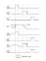
211 撮像動作
212 データ保持動作
213 読み出し動作
2700 画素アレイ
2730 回路
2740 回路
2750 回路
2751 バイアストランジスタアレイ
2760 回路
2761 バイアストランジスタアレイ
3040 シリコン基板
3041 絶縁膜
3041a 絶縁膜
3041b 絶縁膜
3042 絶縁膜
3042a 絶縁膜
3042b 絶縁膜
3055 トランジスタ
3056 トランジスタ
3059 活性層
3061 光電変換膜
3062 透光性導電膜
3063 半導体膜
3064 半導体膜
3065 半導体膜
3066 電極
3067 隔壁
3071 配線
3072 配線
3074 配線
3075 配線
3076 配線
3077 配線
3078 配線
3079 配線
3080 絶縁膜
3081 導電膜
3200 領域
3300 領域
3400 領域
3500 絶縁膜
3510 遮光層
3520 有機樹脂層
3530a カラーフィルタ
3530b カラーフィルタ
3530c カラーフィルタ
3540 マイクロレンズアレイ
3550 光学変換層
4101 トランジスタ
4102 トランジスタ
4103 トランジスタ
4104 トランジスタ
4105 トランジスタ
4106 トランジスタ
4107 トランジスタ
4108 トランジスタ
4109 トランジスタ
4110 トランジスタ
4111 トランジスタ
4112 トランジスタ
4113 トランジスタ
4115 基板
4120 絶縁膜
4130 酸化物半導体膜
4130a 絶縁膜
4130b 酸化物半導体膜
4130c 絶縁膜
4140 導電膜
4141 導電膜
4142 導電膜
4150 導電膜
4151 導電膜
4152 導電膜
4160 絶縁膜
4170 導電膜
4171 導電膜
4172 導電膜
4173 導電膜
4175 絶縁膜
4180 絶縁膜
4190 絶縁膜
4231 領域
4232 領域
4233 領域
4234 領域
4235 領域
4331 領域
4332 領域
4333 領域
4334 領域
4335 領域
6901 筐体
6902 筐体
6903 表示部
6904 表示部
6905 マイク
6906 スピーカー
6907 操作キー
6908 スタイラス
6909 カメラ
6911 筐体
6912 表示部
6919 カメラ
6931 筐体
6932 表示部
6933 リストバンド
6939 カメラ
6951 筐体
6952 表示部
6954 スピーカー
6955 ボタン
6956 入出力端子
6957 マイク
6959 カメラ
6961 筐体
6962 シャッターボタン
6963 マイク
6965 レンズ
6967 発光部
6971 筐体
6972 筐体
6973 表示部
6974 操作キー
6975 レンズ
6976 接続部
Claims (12)
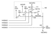
- フォトダイオードと、第1のトランジスタと、第2のトランジスタと、第3のトランジスタと、第4のトランジスタと、を有する画素を有し、
前記第1のトランジスタのソース電極またはドレイン電極の一方は、前記フォトダイオードの一方の電極と電気的に接続され、
前記第1のトランジスタのソース電極または前記ドレイン電極の他方は、前記第2のトランジスタのゲート電極と電気的に接続され、
前記第1のトランジスタのソース電極またはドレイン電極の他方は、前記第3のトランジスタのソース電極またはドレイン電極の一方と電気的に接続され、
前記第2のトランジスタのソース電極またはドレイン電極の一方は、前記第4のトランジスタのソース電極またはドレイン電極の一方と電気的に接続され、
前記第1のトランジスタ、前記第2のトランジスタおよび前記第3のトランジスタはバックゲート電極を有し、
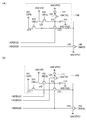
前記第1のトランジスタおよび前記第3のトランジスタのバックゲート電極は、各トランジスタのソース電位より高い電位および各トランジスタのソース電位より低い電位を切り替えて供給することのできる配線と電気的に接続されており、前記第2のトランジスタのバックゲート電極は、前記第2のトランジスタのソース電位より高い電位を供給することのできる配線と電気的に接続されていることを特徴とする撮像装置。 - 前記第1のトランジスタおよび前記第3のトランジスタのバックゲート電極は第1の配線と電気的に接続され、
前記第2のトランジスタのバックゲート電極は第2の配線と電気的に接続され、
前記第1の配線および前記第2の配線は、同じ行または列に配置された前記画素の他、隣接する行または列の、一方の側に配置された前記画素と共有されることを特徴とする、
請求項1に記載の撮像装置。 - 前記第1の配線は、隣接する行または列のうち、上面または下面から見て前記第2のトランジスタを間に挟まない側に配置された前記画素と共有され、
前記第2の配線は、隣接する行または列のうち、前記第1のトランジスタおよび前記第3のトランジスタを間に挟まない側に配置された前記画素と共有されることを特徴とする、
請求項2に記載の撮像装置。 - 画素を複数有し、
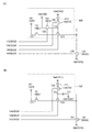
前記画素はフォトダイオードと、第1のトランジスタと、第2のトランジスタと、第3のトランジスタと、第4のトランジスタと、を有し、
前記第1のトランジスタのソース電極またはドレイン電極の一方は、前記フォトダイオードの一方の電極と電気的に接続され、
前記第1のトランジスタのソース電極または前記ドレイン電極の他方は、前記第2のトランジスタのゲート電極と電気的に接続され、
前記第1のトランジスタのソース電極またはドレイン電極の他方は、前記第3のトランジスタのソース電極またはドレイン電極の一方と電気的に接続され、
前記第2のトランジスタのソース電極またはドレイン電極の一方は、前記第4のトランジスタのソース電極またはドレイン電極の一方と電気的に接続され、
前記第1のトランジスタ、前記第2のトランジスタ、前記第3のトランジスタおよび前記第4のトランジスタはバックゲート電極を有し、
前記第1のトランジスタおよび前記第3のトランジスタのバックゲート電極は、各トランジスタのソース電位より高い電位および各トランジスタのソース電位より低い電位を切り替えて供給することのできる配線と電気的に接続されており、前記第2のトランジスタおよび前記第4のトランジスタのバックゲート電極は、各トランジスタのソース電位より高い電位を供給することのできる配線と電気的に接続されていることを特徴とする撮像装置。 - 前記第1のトランジスタおよび前記第3のトランジスタのバックゲート電極は第1の配線と電気的に接続され、
前記第2のトランジスタおよび前記第4のトランジスタのバックゲート電極は第2の配線と電気的に接続され、
前記第1の配線および前記第2の配線は、同じ行または列に配置された前記画素の他、隣接する行または列の、一方の側に配置された前記画素と共有されることを特徴とする、
請求項4に記載の撮像装置。 - 前記第1の配線は、隣接する行または列のうち、上面または下面から見て前記第2のトランジスタおよび前記第4のトランジスタを間に挟まない側に配置された前記画素と共有され、
前記第2の配線は、隣接する行または列のうち、前記第1のトランジスタおよび前記第3のトランジスタを間に挟まない側に配置された前記画素と共有されることを特徴とする、
請求項5に記載の撮像装置。 - 前記第1のトランジスタ、前記第3のトランジスタおよび前記第4のトランジスタが有するバックゲート電極は第1の配線と電気的に接続され、
前記第2のトランジスタのバックゲート電極は第2の配線と電気的に接続され、
前記第1の配線および前記第2の配線は、同じ行または列に配置された前記画素の他、隣接する行または列の、一方の側に配置された前記画素と共有されることを特徴とする、
請求項4に記載の撮像装置。 - 前記第1の配線および前記第2の配線は、隣接する行または列のうち、上面または下面から見て前記第2のトランジスタを間に挟まない側に配置された前記画素と共有され、
前記第2の配線は、隣接する行または列のうち、前記第1のトランジスタ、前記第3のトランジスタおよび前記第4のトランジスタを間に挟まない側に配置された前記画素と共有されることを特徴とする、
請求項7に記載の撮像装置。 - 第5のトランジスタを有し、
前記第5のトランジスタのソース電極またはドレイン電極の一方は前記第2のトランジスタのソース電極またはドレイン電極の他方と電気的に接続され、
前記第5のトランジスタはバックゲート電極を有し、
前記第5のトランジスタのバックゲート電極には、前記第5のトランジスタのソース電位より高い電位を供給することのできる配線と電気的に接続されていることを特徴とする、
請求項1乃至請求項8のいずれか一項に記載の撮像装置。 - 前記第1のトランジスタ、前記第2のトランジスタ、前記第3のトランジスタ、前記第4のトランジスタおよび前記第5のトランジスタが有する活性層が、酸化物半導体を有することを特徴とする、
請求項1乃至請求項9のいずれか一項に記載の撮像装置。 - 前記フォトダイオードは、光電変換膜にセレンを有することを特徴とする、
請求項1乃至請求項10のいずれか一項に記載の撮像装置。 - 請求項1乃至請求項11のいずれか一項に記載の撮像装置と、表示装置と、を有することを特徴とする電子機器。
Applications Claiming Priority (2)
| Application Number | Priority Date | Filing Date | Title |
|---|---|---|---|
| JP2015076420 | 2015-04-03 | ||
| JP2015076420 | 2015-04-03 |
Related Child Applications (1)
| Application Number | Title | Priority Date | Filing Date |
|---|---|---|---|
| JP2020192514A Division JP7019784B2 (ja) | 2015-04-03 | 2020-11-19 | 撮像装置 |
Publications (2)
| Publication Number | Publication Date |
|---|---|
| JP2016197722A true JP2016197722A (ja) | 2016-11-24 |
| JP6798790B2 JP6798790B2 (ja) | 2020-12-09 |
Family
ID=57015343
Family Applications (2)
| Application Number | Title | Priority Date | Filing Date |
|---|---|---|---|
| JP2016073850A Active JP6798790B2 (ja) | 2015-04-03 | 2016-04-01 | 撮像装置および電子機器 |
| JP2020192514A Active JP7019784B2 (ja) | 2015-04-03 | 2020-11-19 | 撮像装置 |
Family Applications After (1)
| Application Number | Title | Priority Date | Filing Date |
|---|---|---|---|
| JP2020192514A Active JP7019784B2 (ja) | 2015-04-03 | 2020-11-19 | 撮像装置 |
Country Status (2)
| Country | Link |
|---|---|
| US (1) | US9685476B2 (ja) |
| JP (2) | JP6798790B2 (ja) |
Cited By (2)
| Publication number | Priority date | Publication date | Assignee | Title |
|---|---|---|---|---|
| JP2018164139A (ja) * | 2017-03-24 | 2018-10-18 | 株式会社半導体エネルギー研究所 | 撮像装置および電子機器 |
| WO2024013808A1 (ja) * | 2022-07-11 | 2024-01-18 | シャープディスプレイテクノロジー株式会社 | 表示装置 |
Families Citing this family (6)
| Publication number | Priority date | Publication date | Assignee | Title |
|---|---|---|---|---|
| US9773832B2 (en) | 2014-12-10 | 2017-09-26 | Semiconductor Energy Laboratory Co., Ltd. | Semiconductor device and electronic device |
| TWI713367B (zh) | 2015-07-07 | 2020-12-11 | 日商半導體能源研究所股份有限公司 | 成像裝置及其運作方法 |
| JP7148269B2 (ja) * | 2018-05-02 | 2022-10-05 | ソニーセミコンダクタソリューションズ株式会社 | 固体撮像素子および撮像装置 |
| CN108766989B (zh) * | 2018-06-01 | 2021-09-03 | 京东方科技集团股份有限公司 | 一种光学传感器件及其制作方法、显示器件、显示设备 |
| KR20200144632A (ko) * | 2019-06-18 | 2020-12-30 | 삼성디스플레이 주식회사 | 표시 장치 및 이의 구동 방법 |
| KR20210013481A (ko) * | 2019-07-26 | 2021-02-04 | 삼성디스플레이 주식회사 | 표시 장치 및 이의 구동 방법 |
Citations (6)
| Publication number | Priority date | Publication date | Assignee | Title |
|---|---|---|---|---|
| JP2001308306A (ja) * | 2000-04-21 | 2001-11-02 | Semiconductor Energy Lab Co Ltd | 半導体装置およびその駆動方法 |
| US20110198483A1 (en) * | 2010-02-12 | 2011-08-18 | Semiconductor Energy Laboratory Co., Ltd. | Semiconductor device and driving method thereof |
| US20110215323A1 (en) * | 2010-03-08 | 2011-09-08 | Semiconductor Energy Laboratory Co., Ltd. | Semiconductor device and manufacturing method thereof |
| JP2012049211A (ja) * | 2010-08-25 | 2012-03-08 | Fujifilm Corp | 酸化物半導体薄膜の製造方法および酸化物半導体薄膜、薄膜トランジスタの製造方法および薄膜トランジスタ、並びに薄膜トランジスタを備えた装置 |
| US20130285046A1 (en) * | 2012-04-25 | 2013-10-31 | Semiconductor Energy Laboratory Co., Ltd. | Semiconductor device and method of manufacturing the same |
| US20130285045A1 (en) * | 2012-04-27 | 2013-10-31 | Semiconductor Energy Laboratory Co., Ltd. | Oxide semiconductor film and semiconductor device |
Family Cites Families (18)
| Publication number | Priority date | Publication date | Assignee | Title |
|---|---|---|---|---|
| JP3316702B2 (ja) * | 1993-03-31 | 2002-08-19 | カシオ計算機株式会社 | 画像読取装置 |
| EP1998375A3 (en) | 2005-09-29 | 2012-01-18 | Semiconductor Energy Laboratory Co, Ltd. | Semiconductor device having oxide semiconductor layer and manufacturing method |
| JP5064747B2 (ja) | 2005-09-29 | 2012-10-31 | 株式会社半導体エネルギー研究所 | 半導体装置、電気泳動表示装置、表示モジュール、電子機器、及び半導体装置の作製方法 |
| JP5078246B2 (ja) | 2005-09-29 | 2012-11-21 | 株式会社半導体エネルギー研究所 | 半導体装置、及び半導体装置の作製方法 |
| US7663165B2 (en) | 2006-08-31 | 2010-02-16 | Aptina Imaging Corporation | Transparent-channel thin-film transistor-based pixels for high-performance image sensors |
| JP5190275B2 (ja) * | 2008-01-09 | 2013-04-24 | パナソニック株式会社 | 半導体メモリセル及びそれを用いた半導体メモリアレイ |
| KR101842182B1 (ko) * | 2009-05-01 | 2018-03-26 | 가부시키가이샤 한도오따이 에네루기 켄큐쇼 | 반도체 장치의 제작 방법 |
| WO2011027664A1 (en) * | 2009-09-04 | 2011-03-10 | Semiconductor Energy Laboratory Co., Ltd. | Liquid crystal display device and method for manufacturing the same |
| KR101952065B1 (ko) | 2009-11-06 | 2019-02-25 | 가부시키가이샤 한도오따이 에네루기 켄큐쇼 | 반도체 장치 및 그 동작 방법 |
| KR101488521B1 (ko) | 2009-11-06 | 2015-02-02 | 가부시키가이샤 한도오따이 에네루기 켄큐쇼 | 반도체 장치 |
| WO2011099343A1 (en) | 2010-02-12 | 2011-08-18 | Semiconductor Energy Laboratory Co., Ltd. | Semiconductor device and driving method thereof |
| JP2012033835A (ja) * | 2010-08-03 | 2012-02-16 | Canon Inc | 光電子素子の駆動方法及び該駆動方法で駆動される光電子装置 |
| JP5935287B2 (ja) * | 2011-10-21 | 2016-06-15 | ソニー株式会社 | 撮像装置および撮像表示システム |
| US9035301B2 (en) * | 2013-06-19 | 2015-05-19 | Semiconductor Energy Laboratory Co., Ltd. | Imaging device |
| US9360564B2 (en) * | 2013-08-30 | 2016-06-07 | Semiconductor Energy Laboratory Co., Ltd. | Imaging device |
| US9881954B2 (en) * | 2014-06-11 | 2018-01-30 | Semiconductor Energy Laboratory Co., Ltd. | Imaging device |
| TWI700823B (zh) * | 2014-06-27 | 2020-08-01 | 日商半導體能源研究所股份有限公司 | 攝像裝置及電子裝置 |
| KR20170072889A (ko) | 2014-10-10 | 2017-06-27 | 가부시키가이샤 한도오따이 에네루기 켄큐쇼 | 촬상 장치 |
-
2016
- 2016-03-29 US US15/083,755 patent/US9685476B2/en active Active
- 2016-04-01 JP JP2016073850A patent/JP6798790B2/ja active Active
-
2020
- 2020-11-19 JP JP2020192514A patent/JP7019784B2/ja active Active
Patent Citations (12)
| Publication number | Priority date | Publication date | Assignee | Title |
|---|---|---|---|---|
| JP2001308306A (ja) * | 2000-04-21 | 2001-11-02 | Semiconductor Energy Lab Co Ltd | 半導体装置およびその駆動方法 |
| US20110198483A1 (en) * | 2010-02-12 | 2011-08-18 | Semiconductor Energy Laboratory Co., Ltd. | Semiconductor device and driving method thereof |
| WO2011099336A1 (en) * | 2010-02-12 | 2011-08-18 | Semiconductor Energy Laboratory Co., Ltd. | Semiconductor device and driving method thereof |
| JP2011187944A (ja) * | 2010-02-12 | 2011-09-22 | Semiconductor Energy Lab Co Ltd | 半導体装置およびその駆動方法 |
| US20110215323A1 (en) * | 2010-03-08 | 2011-09-08 | Semiconductor Energy Laboratory Co., Ltd. | Semiconductor device and manufacturing method thereof |
| WO2011111549A1 (en) * | 2010-03-08 | 2011-09-15 | Semiconductor Energy Laboratory Co., Ltd. | Semiconductor device and manufacturing method thereof |
| JP2011211699A (ja) * | 2010-03-08 | 2011-10-20 | Semiconductor Energy Lab Co Ltd | 半導体装置、及びその駆動方法 |
| JP2012049211A (ja) * | 2010-08-25 | 2012-03-08 | Fujifilm Corp | 酸化物半導体薄膜の製造方法および酸化物半導体薄膜、薄膜トランジスタの製造方法および薄膜トランジスタ、並びに薄膜トランジスタを備えた装置 |
| US20130285046A1 (en) * | 2012-04-25 | 2013-10-31 | Semiconductor Energy Laboratory Co., Ltd. | Semiconductor device and method of manufacturing the same |
| JP2013243355A (ja) * | 2012-04-25 | 2013-12-05 | Semiconductor Energy Lab Co Ltd | 半導体装置およびその作製方法 |
| US20130285045A1 (en) * | 2012-04-27 | 2013-10-31 | Semiconductor Energy Laboratory Co., Ltd. | Oxide semiconductor film and semiconductor device |
| JP2013243352A (ja) * | 2012-04-27 | 2013-12-05 | Semiconductor Energy Lab Co Ltd | 酸化物半導体膜および半導体装置 |
Cited By (2)
| Publication number | Priority date | Publication date | Assignee | Title |
|---|---|---|---|---|
| JP2018164139A (ja) * | 2017-03-24 | 2018-10-18 | 株式会社半導体エネルギー研究所 | 撮像装置および電子機器 |
| WO2024013808A1 (ja) * | 2022-07-11 | 2024-01-18 | シャープディスプレイテクノロジー株式会社 | 表示装置 |
Also Published As
| Publication number | Publication date |
|---|---|
| JP6798790B2 (ja) | 2020-12-09 |
| US9685476B2 (en) | 2017-06-20 |
| JP7019784B2 (ja) | 2022-02-15 |
| JP2021036614A (ja) | 2021-03-04 |
| US20160293655A1 (en) | 2016-10-06 |
Similar Documents
| Publication | Publication Date | Title |
|---|---|---|
| JP7142120B2 (ja) | 撮像装置 | |
| JP7432644B2 (ja) | 撮像装置 | |
| JP7049413B2 (ja) | 電子機器 | |
| JP6745955B2 (ja) | 撮像装置 | |
| JP6692681B2 (ja) | 撮像装置の駆動方法 | |
| JP6734132B2 (ja) | 撮像装置 | |
| JP7019784B2 (ja) | 撮像装置 | |
| JP6688116B2 (ja) | 撮像装置および電子機器 | |
| JP2019216244A (ja) | 撮像装置 | |
| JP2016213471A (ja) | 撮像装置および電子機器 | |
| JP6749781B2 (ja) | 撮像装置 | |
| JP2017005713A (ja) | 撮像装置、その動作方法および電子機器 | |
| JP6689121B2 (ja) | 撮像装置および電子機器 | |
| JP6647884B2 (ja) | 撮像装置および電子機器 | |
| JP2020096375A (ja) | 撮像装置 |
Legal Events
| Date | Code | Title | Description |
|---|---|---|---|
| A621 | Written request for application examination |
Free format text: JAPANESE INTERMEDIATE CODE: A621 Effective date: 20190401 |
|
| A977 | Report on retrieval |
Free format text: JAPANESE INTERMEDIATE CODE: A971007 Effective date: 20200227 |
|
| A131 | Notification of reasons for refusal |
Free format text: JAPANESE INTERMEDIATE CODE: A131 Effective date: 20200303 |
|
| A521 | Request for written amendment filed |
Free format text: JAPANESE INTERMEDIATE CODE: A523 Effective date: 20200430 |
|
| A131 | Notification of reasons for refusal |
Free format text: JAPANESE INTERMEDIATE CODE: A131 Effective date: 20200616 |
|
| A601 | Written request for extension of time |
Free format text: JAPANESE INTERMEDIATE CODE: A601 Effective date: 20200811 |
|
| A521 | Request for written amendment filed |
Free format text: JAPANESE INTERMEDIATE CODE: A523 Effective date: 20201008 |
|
| TRDD | Decision of grant or rejection written | ||
| A01 | Written decision to grant a patent or to grant a registration (utility model) |
Free format text: JAPANESE INTERMEDIATE CODE: A01 Effective date: 20201027 |
|
| A61 | First payment of annual fees (during grant procedure) |
Free format text: JAPANESE INTERMEDIATE CODE: A61 Effective date: 20201119 |
|
| R150 | Certificate of patent or registration of utility model |
Ref document number: 6798790 Country of ref document: JP Free format text: JAPANESE INTERMEDIATE CODE: R150 |
|
| R250 | Receipt of annual fees |
Free format text: JAPANESE INTERMEDIATE CODE: R250 |