JP2016130820A - 表示装置及び照明装置 - Google Patents
表示装置及び照明装置 Download PDFInfo
- Publication number
- JP2016130820A JP2016130820A JP2015005636A JP2015005636A JP2016130820A JP 2016130820 A JP2016130820 A JP 2016130820A JP 2015005636 A JP2015005636 A JP 2015005636A JP 2015005636 A JP2015005636 A JP 2015005636A JP 2016130820 A JP2016130820 A JP 2016130820A
- Authority
- JP
- Japan
- Prior art keywords
- light
- substrate
- liquid crystal
- backlight
- facing
- Prior art date
- Legal status (The legal status is an assumption and is not a legal conclusion. Google has not performed a legal analysis and makes no representation as to the accuracy of the status listed.)
- Pending
Links
Images


Classifications
-
- G—PHYSICS
- G02—OPTICS
- G02B—OPTICAL ELEMENTS, SYSTEMS OR APPARATUS
- G02B6/00—Light guides; Structural details of arrangements comprising light guides and other optical elements, e.g. couplings
- G02B6/0001—Light guides; Structural details of arrangements comprising light guides and other optical elements, e.g. couplings specially adapted for lighting devices or systems
- G02B6/0011—Light guides; Structural details of arrangements comprising light guides and other optical elements, e.g. couplings specially adapted for lighting devices or systems the light guides being planar or of plate-like form
- G02B6/0081—Mechanical or electrical aspects of the light guide and light source in the lighting device peculiar to the adaptation to planar light guides, e.g. concerning packaging
- G02B6/0086—Positioning aspects
- G02B6/0091—Positioning aspects of the light source relative to the light guide
-
- G—PHYSICS
- G02—OPTICS
- G02B—OPTICAL ELEMENTS, SYSTEMS OR APPARATUS
- G02B6/00—Light guides; Structural details of arrangements comprising light guides and other optical elements, e.g. couplings
- G02B6/0001—Light guides; Structural details of arrangements comprising light guides and other optical elements, e.g. couplings specially adapted for lighting devices or systems
- G02B6/0011—Light guides; Structural details of arrangements comprising light guides and other optical elements, e.g. couplings specially adapted for lighting devices or systems the light guides being planar or of plate-like form
- G02B6/0013—Means for improving the coupling-in of light from the light source into the light guide
- G02B6/0023—Means for improving the coupling-in of light from the light source into the light guide provided by one optical element, or plurality thereof, placed between the light guide and the light source, or around the light source
- G02B6/0028—Light guide, e.g. taper
-
- G—PHYSICS
- G02—OPTICS
- G02F—OPTICAL DEVICES OR ARRANGEMENTS FOR THE CONTROL OF LIGHT BY MODIFICATION OF THE OPTICAL PROPERTIES OF THE MEDIA OF THE ELEMENTS INVOLVED THEREIN; NON-LINEAR OPTICS; FREQUENCY-CHANGING OF LIGHT; OPTICAL LOGIC ELEMENTS; OPTICAL ANALOGUE/DIGITAL CONVERTERS
- G02F1/00—Devices or arrangements for the control of the intensity, colour, phase, polarisation or direction of light arriving from an independent light source, e.g. switching, gating or modulating; Non-linear optics
- G02F1/01—Devices or arrangements for the control of the intensity, colour, phase, polarisation or direction of light arriving from an independent light source, e.g. switching, gating or modulating; Non-linear optics for the control of the intensity, phase, polarisation or colour
- G02F1/13—Devices or arrangements for the control of the intensity, colour, phase, polarisation or direction of light arriving from an independent light source, e.g. switching, gating or modulating; Non-linear optics for the control of the intensity, phase, polarisation or colour based on liquid crystals, e.g. single liquid crystal display cells
- G02F1/133—Constructional arrangements; Operation of liquid crystal cells; Circuit arrangements
- G02F1/1333—Constructional arrangements; Manufacturing methods
- G02F1/133345—Insulating layers
-
- G—PHYSICS
- G02—OPTICS
- G02F—OPTICAL DEVICES OR ARRANGEMENTS FOR THE CONTROL OF LIGHT BY MODIFICATION OF THE OPTICAL PROPERTIES OF THE MEDIA OF THE ELEMENTS INVOLVED THEREIN; NON-LINEAR OPTICS; FREQUENCY-CHANGING OF LIGHT; OPTICAL LOGIC ELEMENTS; OPTICAL ANALOGUE/DIGITAL CONVERTERS
- G02F1/00—Devices or arrangements for the control of the intensity, colour, phase, polarisation or direction of light arriving from an independent light source, e.g. switching, gating or modulating; Non-linear optics
- G02F1/01—Devices or arrangements for the control of the intensity, colour, phase, polarisation or direction of light arriving from an independent light source, e.g. switching, gating or modulating; Non-linear optics for the control of the intensity, phase, polarisation or colour
- G02F1/13—Devices or arrangements for the control of the intensity, colour, phase, polarisation or direction of light arriving from an independent light source, e.g. switching, gating or modulating; Non-linear optics for the control of the intensity, phase, polarisation or colour based on liquid crystals, e.g. single liquid crystal display cells
- G02F1/133—Constructional arrangements; Operation of liquid crystal cells; Circuit arrangements
- G02F1/1333—Constructional arrangements; Manufacturing methods
- G02F1/1339—Gaskets; Spacers; Sealing of cells
-
- G—PHYSICS
- G02—OPTICS
- G02F—OPTICAL DEVICES OR ARRANGEMENTS FOR THE CONTROL OF LIGHT BY MODIFICATION OF THE OPTICAL PROPERTIES OF THE MEDIA OF THE ELEMENTS INVOLVED THEREIN; NON-LINEAR OPTICS; FREQUENCY-CHANGING OF LIGHT; OPTICAL LOGIC ELEMENTS; OPTICAL ANALOGUE/DIGITAL CONVERTERS
- G02F1/00—Devices or arrangements for the control of the intensity, colour, phase, polarisation or direction of light arriving from an independent light source, e.g. switching, gating or modulating; Non-linear optics
- G02F1/01—Devices or arrangements for the control of the intensity, colour, phase, polarisation or direction of light arriving from an independent light source, e.g. switching, gating or modulating; Non-linear optics for the control of the intensity, phase, polarisation or colour
- G02F1/13—Devices or arrangements for the control of the intensity, colour, phase, polarisation or direction of light arriving from an independent light source, e.g. switching, gating or modulating; Non-linear optics for the control of the intensity, phase, polarisation or colour based on liquid crystals, e.g. single liquid crystal display cells
- G02F1/133—Constructional arrangements; Operation of liquid crystal cells; Circuit arrangements
- G02F1/1333—Constructional arrangements; Manufacturing methods
- G02F1/1343—Electrodes
- G02F1/134309—Electrodes characterised by their geometrical arrangement
-
- G—PHYSICS
- G02—OPTICS
- G02F—OPTICAL DEVICES OR ARRANGEMENTS FOR THE CONTROL OF LIGHT BY MODIFICATION OF THE OPTICAL PROPERTIES OF THE MEDIA OF THE ELEMENTS INVOLVED THEREIN; NON-LINEAR OPTICS; FREQUENCY-CHANGING OF LIGHT; OPTICAL LOGIC ELEMENTS; OPTICAL ANALOGUE/DIGITAL CONVERTERS
- G02F1/00—Devices or arrangements for the control of the intensity, colour, phase, polarisation or direction of light arriving from an independent light source, e.g. switching, gating or modulating; Non-linear optics
- G02F1/01—Devices or arrangements for the control of the intensity, colour, phase, polarisation or direction of light arriving from an independent light source, e.g. switching, gating or modulating; Non-linear optics for the control of the intensity, phase, polarisation or colour
- G02F1/13—Devices or arrangements for the control of the intensity, colour, phase, polarisation or direction of light arriving from an independent light source, e.g. switching, gating or modulating; Non-linear optics for the control of the intensity, phase, polarisation or colour based on liquid crystals, e.g. single liquid crystal display cells
- G02F1/133—Constructional arrangements; Operation of liquid crystal cells; Circuit arrangements
- G02F1/1333—Constructional arrangements; Manufacturing methods
- G02F1/1345—Conductors connecting electrodes to cell terminals
- G02F1/13452—Conductors connecting driver circuitry and terminals of panels
-
- G—PHYSICS
- G02—OPTICS
- G02F—OPTICAL DEVICES OR ARRANGEMENTS FOR THE CONTROL OF LIGHT BY MODIFICATION OF THE OPTICAL PROPERTIES OF THE MEDIA OF THE ELEMENTS INVOLVED THEREIN; NON-LINEAR OPTICS; FREQUENCY-CHANGING OF LIGHT; OPTICAL LOGIC ELEMENTS; OPTICAL ANALOGUE/DIGITAL CONVERTERS
- G02F1/00—Devices or arrangements for the control of the intensity, colour, phase, polarisation or direction of light arriving from an independent light source, e.g. switching, gating or modulating; Non-linear optics
- G02F1/01—Devices or arrangements for the control of the intensity, colour, phase, polarisation or direction of light arriving from an independent light source, e.g. switching, gating or modulating; Non-linear optics for the control of the intensity, phase, polarisation or colour
- G02F1/13—Devices or arrangements for the control of the intensity, colour, phase, polarisation or direction of light arriving from an independent light source, e.g. switching, gating or modulating; Non-linear optics for the control of the intensity, phase, polarisation or colour based on liquid crystals, e.g. single liquid crystal display cells
- G02F1/133—Constructional arrangements; Operation of liquid crystal cells; Circuit arrangements
- G02F1/136—Liquid crystal cells structurally associated with a semi-conducting layer or substrate, e.g. cells forming part of an integrated circuit
-
- G—PHYSICS
- G02—OPTICS
- G02B—OPTICAL ELEMENTS, SYSTEMS OR APPARATUS
- G02B6/00—Light guides; Structural details of arrangements comprising light guides and other optical elements, e.g. couplings
- G02B6/0001—Light guides; Structural details of arrangements comprising light guides and other optical elements, e.g. couplings specially adapted for lighting devices or systems
- G02B6/0011—Light guides; Structural details of arrangements comprising light guides and other optical elements, e.g. couplings specially adapted for lighting devices or systems the light guides being planar or of plate-like form
- G02B6/0013—Means for improving the coupling-in of light from the light source into the light guide
- G02B6/0023—Means for improving the coupling-in of light from the light source into the light guide provided by one optical element, or plurality thereof, placed between the light guide and the light source, or around the light source
- G02B6/0031—Reflecting element, sheet or layer
-
- G—PHYSICS
- G02—OPTICS
- G02B—OPTICAL ELEMENTS, SYSTEMS OR APPARATUS
- G02B6/00—Light guides; Structural details of arrangements comprising light guides and other optical elements, e.g. couplings
- G02B6/0001—Light guides; Structural details of arrangements comprising light guides and other optical elements, e.g. couplings specially adapted for lighting devices or systems
- G02B6/0011—Light guides; Structural details of arrangements comprising light guides and other optical elements, e.g. couplings specially adapted for lighting devices or systems the light guides being planar or of plate-like form
- G02B6/0081—Mechanical or electrical aspects of the light guide and light source in the lighting device peculiar to the adaptation to planar light guides, e.g. concerning packaging
- G02B6/0083—Details of electrical connections of light sources to drivers, circuit boards, or the like
-
- G—PHYSICS
- G02—OPTICS
- G02F—OPTICAL DEVICES OR ARRANGEMENTS FOR THE CONTROL OF LIGHT BY MODIFICATION OF THE OPTICAL PROPERTIES OF THE MEDIA OF THE ELEMENTS INVOLVED THEREIN; NON-LINEAR OPTICS; FREQUENCY-CHANGING OF LIGHT; OPTICAL LOGIC ELEMENTS; OPTICAL ANALOGUE/DIGITAL CONVERTERS
- G02F1/00—Devices or arrangements for the control of the intensity, colour, phase, polarisation or direction of light arriving from an independent light source, e.g. switching, gating or modulating; Non-linear optics
- G02F1/01—Devices or arrangements for the control of the intensity, colour, phase, polarisation or direction of light arriving from an independent light source, e.g. switching, gating or modulating; Non-linear optics for the control of the intensity, phase, polarisation or colour
- G02F1/13—Devices or arrangements for the control of the intensity, colour, phase, polarisation or direction of light arriving from an independent light source, e.g. switching, gating or modulating; Non-linear optics for the control of the intensity, phase, polarisation or colour based on liquid crystals, e.g. single liquid crystal display cells
- G02F1/133—Constructional arrangements; Operation of liquid crystal cells; Circuit arrangements
- G02F1/1333—Constructional arrangements; Manufacturing methods
- G02F1/1335—Structural association of cells with optical devices, e.g. polarisers or reflectors
- G02F1/1336—Illuminating devices
- G02F1/133615—Edge-illuminating devices, i.e. illuminating from the side
Abstract
Description
表示パネルに重ねられた面光源型のバックライトなどの照明装置からの光を用いて画像を表示する表示装置において、額縁領域を狭めるためには、表示パネルだけでなく照明装置の設計も最適化しなければならない。
なお、開示はあくまで一例に過ぎず、当業者において、発明の主旨を保っての適宜変更について容易に想到し得るものについては、当然に本発明の範囲に含有される。また、図面は、説明をより明確にするため、実際の態様に比べて、各部の幅、厚さ、形状等について模式的に表される場合があるが、あくまで一例であって、本発明の解釈を限定するものではない。各図において、連続して配置される同一又は類似の要素については符号を省略することがある。また、本明細書と各図において、既出の図に関して前述したものと同一又は類似した機能を発揮する構成要素には同一の参照符号を付し、重複する詳細な説明を省略することがある。
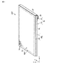
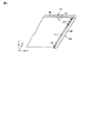
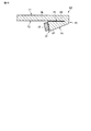
図1は、第1実施形態に係る液晶表示装置DSPを概略的に示す斜視図である。液晶表示装置DSPは、アクティブマトリクス型の液晶表示パネルPNLと、バックライトBLと、を備えている。図1の例において、液晶表示パネルPNL及びバックライトBLは、第1方向Xに沿う一対の辺と、第1方向Xと直交する第2方向Yに沿う一対の辺とを有する矩形状であり、第1方向X及び第2方向Yとそれぞれ直交する第3方向Zに重ねられている。液晶表示パネルPNL及びバックライトBLの第1方向Xに沿う辺は例えば短辺であり、第2方向Yに沿う辺は例えば長辺である。液晶表示パネルPNL及びバックライトBLは矩形状に限られず、他の形状であっても良い。
液晶表示パネルPNLは、表示領域DAにおいて、複数の画素PXを備えている。複数の画素PXは、例えば、第1方向X及び第2方向Yに沿ってマトリクス状に配列されている。
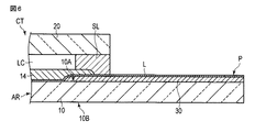
第1絶縁基板10の第1主面10Aは、アンダーコート層11によって覆われている。薄膜トランジスタTrは、アンダーコート層11の上に形成されている。図示した例では、薄膜トランジスタTrはトップゲート型に構成されているが、ボトムゲート型であっても良い。薄膜トランジスタTrは、アンダーコート層11の上に形成された半導体層SCを備えている。半導体層SCは、第1絶縁層12によって覆われている。また、第1絶縁層12は、アンダーコート層11の上にも配置されている。
薄膜トランジスタTrのソース電極WS及びドレイン電極WDは、第2絶縁層13の上に形成されている。また、ソース配線Sも同様に第2絶縁層13の上に形成されている。ソース電極WSは、ソース配線Sと電気的に接続されている。ソース電極WSは、ソース配線Sと一体的に形成されても良い。ソース電極WSは第1絶縁層12及び第2絶縁層13を貫通するコンタクトホールCH1を通して半導体層SCと接触し、ドレイン電極WDは第1絶縁層12及び第2絶縁層13を貫通するコンタクトホールCH2を通して半導体層SCと接触している。薄膜トランジスタTrは、第3絶縁層14によって覆われている。第3絶縁層14は、第2絶縁層13の上にも配置されている。このような第3絶縁層14は、例えば、透明な樹脂などの有機系材料によって形成され、薄膜トランジスタTrにより生じる凹凸を平坦化する役割を担う。
さらに、対向基板CTは、第2絶縁基板20と液晶層LCとの間に、遮光層21、カラーフィルタ層22、オーバーコート層23、共通電極CE、及び第2配向膜AL2などを備えている。
共通電極CEは、オーバーコート層23のアレイ基板ARと対向する側の面に形成されている。このような共通電極CEは、例えば、ITOやIZOなどの透明な導電材料によって形成されている。共通電極CEは、第2配向膜AL2によって覆われている。
図5の例において、アレイ基板AR(第1絶縁基板10)と対向基板CT(第2絶縁基板20)の端部は概ね揃っており、これら端部の近傍に配置されたシール材SLを介してアレイ基板AR及び対向基板CTが貼り合わされている。但し、アレイ基板AR及び対向基板CTの端部は必ずしも揃っている必要はなく、一方が他方より突出しても良い。
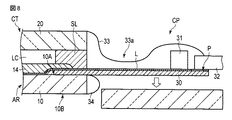
このような保護層33によって接続配線L、パッドP、ドライブIC31の接続配線Lとの接続端子、及び、フレキシブル配線基板32のパッドPとの接続端子等の腐食が防止される。さらに、保護層33によって接続部CPの強度が保たれるとともに、接続配線Lの断線やベース層30の損傷が防がれる。
保護層33及びクッション34は、例えば樹脂材料で形成されている。この場合において、保護層33及びクッション34は、例えばディスペンサによりこれらの元となる樹脂材料を塗布することで形成することができる。
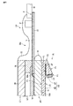
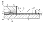
第2端部E2の側において、助走部APは、主導光部MLと接続されている。助走部AP及び主導光部MLは、例えば同一の材料によって一体的に形成されている。このようにすることで、助走部AP及び主導光部MLの接続部分における光学的な界面を無くすことができる。
第4面F4の第3面F3に対する傾きの角度としては、助走部APから主導光部MLへの光の効率的な伝播を可能とする観点、及び、導光板LGの形状を決定する他の要因を考慮して、適宜の値を用いることができる。
先ず、大サイズの第1絶縁基板10上に定義された複数の領域にベース層30及び接続配線L等を含むアレイ基板AR側の各要素を形成し、当該大サイズの第1絶縁基板10から各領域を切り離すことで、アレイ基板ARを製造する。一方で、大サイズの第2絶縁基板20上に定義された複数の領域に対向基板CT側の各要素を形成し、当該大サイズの第2絶縁基板20から各領域を切り離すことで、対向基板CTを製造する。そして、これらアレイ基板AR及び対向基板CTのいずれか一方にシール材SLを塗布するとともに液晶材料を滴下し、両基板を貼り合せる。液晶材料は両基板の間で均一に広がり、液晶層LCを形成する。液晶材料は、両基板の貼り合せの後に両基板の間に注入されても良い。
続いて、図7に示すように、接続部CPにドライブIC31及びフレキシブル配線基板32を実装し、保護層33を形成する。
その他にも、本実施形態からは種々の好適な作用が得られる。
第2実施形態について説明する。ここでは、第1実施形態との差異に着目し、第1実施形態と同一又は類似の要素及び作用については説明を省略する。
図10は、第2実施形態に係る液晶表示装置DSPにおいて、接続部CPが設けられた端部近傍の断面を概略的に示す図である。ここでは、液晶表示パネルPNLが備える要素のうち接続部CPの説明に必要な要素と、バックライトBLの各要素とを示し、他の要素を省略している。
第3絶縁層14の端部及び延伸層40の上には、第2接続配線L2が配置されている。この第2接続配線L2は、第3絶縁層14に設けられたコンタクトホールCH41を通じて第1接続配線L1と電気的に接続されている。
非対向領域NCにおいて、延伸層40には、第2接続配線L2と電気的に接続されたパッドP1が形成されている。パッドP1は、端子部の一例であり、第1接続配線L1、第2接続配線L2、及び、ゲートドライバGD或いはソースドライバSDなどを介して、薄膜トランジスタTrと電気的に接続されている。液晶表示装置DSPは、第1実施形態における接続配線L及びパッドPと同じく第1接続配線L1、第2接続配線L2及びパッドP1を複数備えている。これら複数の第1接続配線L1、第2接続配線L2及びパッドP1の構造は、図10に示したものと同様である。
このような構造においては、フレキシブル配線基板43から供給される画素PXを駆動するための信号が伝達部材42によりパッドP1に伝達され、さらにこの信号が第2接続配線L2及び第1接続配線L1を介してゲートドライバGD及びソースドライバSDなどに伝達される。
第3実施形態について説明する。本実施形態は、導光板LGの構造の変形例であり、第1実施形態、第2実施形態、及び、後述の各実施形態のいずれにも適用できる。
図11は、第3実施形態に係る導光板LGの端部近傍の断面を概略的に示す図である。この図に示した構造は、主導光部MLの第2面F2と助走部APの第3面F3との間に、空間SPに代えて、反射層RFが設けられている点で、上述の各実施形態と相違する。反射層RFは、第3面F3から漏れる光を助走部APに戻すとともに、第2面F2から漏れる光を主導光部MLに戻す。
(第4実施形態)
第4実施形態について説明する。ここでは、第1実施形態との差異に着目し、第1実施形態と同一又は類似の要素及び作用については説明を省略する。
第3絶縁層14は有機材料で形成されているために、水分により腐食され易い。したがって、図5に示したように第3絶縁層14がシール材SLとベース層30との間に延出していると、仮にシール材SLとベース層30との間などから水分が浸入した場合に、この水分によって第3絶縁層14が浸食される恐れがある。
第5実施形態について説明する。ここでは、第1実施形態との差異に着目し、第1実施形態と同一又は類似の要素及び作用については説明を省略する。
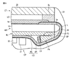
図13は、第5実施形態に係る液晶表示装置DSPの液晶表示パネルPNLにおいて、接続部CPが設けられた端部近傍の断面を概略的に示す図である。この図においては、第4実施形態と同じく第3絶縁層14の端部とベース層30の端部の間にギャップGPが形成されている点、及び、接続部CPにおいて接続配線Lがベース層30の内部に形成されている点で、図5に示した構造と相違する。
接続部CPを曲げる際には、外周側となる面に大きな引っ張り応力が生じる。したがって、図5に示した構造においては、接続部CPがバックライトBLの側に曲げられると、接続配線Lに大きな負荷が生じ、断線を招く可能性がある。
本発明のいくつかの実施形態を説明したが、これらの実施形態は、例として提示したものであり、発明の範囲を限定することは意図していない。これら新規な実施形態は、その他の様々な形態で実施されることが可能であり、発明の要旨を逸脱しない範囲で、種々の省略、置き換え、変更を行うことができる。これら実施形態やその変形は、発明の範囲や要旨に含まれるとともに、特許請求の範囲に記載された発明とその均等の範囲に含まれる。
Claims (7)
- バックライトと、
前記バックライトからの光を選択的に透過する表示パネルと、
を備え、
前記バックライトは、
光源と、
前記表示パネルに対向する第1面と、前記第1面の反対側の第2面と、を有する平板状の主導光部と、
前記第2面の側に配置され、前記第2面と対向する第3面と、前記第3面の反対側の第4面と、前記光源と対向する第1端部と、前記第1端部の反対側に位置し前記主導光部に接続された第2端部とを有し、前記第4面が前記第3面に対して傾いた助走部と、
を備え、
前記光源からの光は、前記第1端部から前記助走部に入射し、前記助走部を前記第2端部に向けて伝播し、そこから前記主導光部に入り、前記主導光部を伝播するとともに前記第1面から出射する、
表示装置。 - 前記表示パネルは、
絶縁基板と、
画像が表示される表示領域において、前記絶縁基板に形成された画素電極と、
前記画素電極と電気的に接続されたスイッチング素子と、
前記表示領域の周囲の非表示領域において、前記絶縁基板の主面の少なくとも一部を覆うとともに、前記絶縁基板の端部から延出した可撓性及び絶縁性を有するベース層と、
前記スイッチング素子と電気的に接続されるとともに、前記ベース層に形成されて前記ベース層と共に前記絶縁基板の端部から延出した配線と、
を備える、
請求項1に記載の表示装置。 - 前記表示パネルは、
前記バックライトと対向する第1基板と、
前記第1基板と対向する第2基板と、
前記第1基板及び前記第2基板のいずれか一方に設けられた画素電極及びこの画素電極と電気的に接続されたスイッチング素子と、
前記スイッチング素子に供給される信号を伝達する伝達部材と、
を備え、
前記第2基板は、前記第1基板よりも外形が大きく、前記バックライト側の面であって且つ前記第1基板と対向しない位置に、前記スイッチング素子と電気的に接続された端子部を備え、
前記伝達部材は、前記端子部と電気的に接続されるとともに、前記主導光部の前記第2面の側に延びている、
請求項1に記載の表示装置。 - 光源と、
第1面と、前記第1面の反対側の第2面と、を有する平板状の主導光部と、
前記第2面の側に配置され、前記第2面と対向する第3面と、前記第3面の反対側の第4面と、前記光源と対向する第1端部と、前記第1端部の反対側に位置し前記主導光部に接続された第2端部とを有し、前記第4面が前記第3面に対して傾いた助走部と、
を備え、
前記光源からの光は、前記第1端部から前記助走部に入射し、前記助走部を前記第2端部に向けて伝播し、そこから前記主導光部に入り、前記主導光部を伝播するとともに前記第1面から出射する、
照明装置。 - 前記第2面と前記第3面との間に空間又は反射層が設けられた、
請求項4に記載の照明装置。 - 前記第4面は、前記助走部の厚さが前記第1端部から前記第2端部に向かうに連れて減少するように前記第3面に対して傾いた、
請求項4又は5に記載の照明装置。 - 前記主導光部及び前記助走部は、同一の材料によって一体的に形成された、
請求項4乃至6のうちいずれか1項に記載の照明装置。
Priority Applications (2)
| Application Number | Priority Date | Filing Date | Title |
|---|---|---|---|
| JP2015005636A JP2016130820A (ja) | 2015-01-15 | 2015-01-15 | 表示装置及び照明装置 |
| US14/988,900 US10401560B2 (en) | 2015-01-15 | 2016-01-06 | Display device including an insulating substrate and a pixel electrode |
Applications Claiming Priority (1)
| Application Number | Priority Date | Filing Date | Title |
|---|---|---|---|
| JP2015005636A JP2016130820A (ja) | 2015-01-15 | 2015-01-15 | 表示装置及び照明装置 |
Publications (2)
| Publication Number | Publication Date |
|---|---|
| JP2016130820A true JP2016130820A (ja) | 2016-07-21 |
| JP2016130820A5 JP2016130820A5 (ja) | 2018-02-01 |
Family
ID=56407723
Family Applications (1)
| Application Number | Title | Priority Date | Filing Date |
|---|---|---|---|
| JP2015005636A Pending JP2016130820A (ja) | 2015-01-15 | 2015-01-15 | 表示装置及び照明装置 |
Country Status (2)
| Country | Link |
|---|---|
| US (1) | US10401560B2 (ja) |
| JP (1) | JP2016130820A (ja) |
Cited By (1)
| Publication number | Priority date | Publication date | Assignee | Title |
|---|---|---|---|---|
| JP2020165996A (ja) * | 2019-03-28 | 2020-10-08 | 東レ株式会社 | 有機電子デバイスの製造方法 |
Families Citing this family (13)
| Publication number | Priority date | Publication date | Assignee | Title |
|---|---|---|---|---|
| JP2016099463A (ja) * | 2014-11-20 | 2016-05-30 | 株式会社ジャパンディスプレイ | 液晶表示装置 |
| JP2017181815A (ja) * | 2016-03-30 | 2017-10-05 | パナソニック液晶ディスプレイ株式会社 | 液晶表示装置 |
| CN107346074A (zh) * | 2016-05-04 | 2017-11-14 | 群创光电股份有限公司 | 显示面板 |
| CN108227317A (zh) * | 2016-12-14 | 2018-06-29 | 群创光电股份有限公司 | 显示装置 |
| US10416509B2 (en) * | 2017-07-31 | 2019-09-17 | Shenzhen China Star Optoelectronics Technology Co., Ltd | Display panel, electronic device, and display panel fabrication method |
| CN107247355A (zh) * | 2017-07-31 | 2017-10-13 | 深圳市华星光电技术有限公司 | 显示面板、电子设备及显示面板的制作方法 |
| CN108037624A (zh) * | 2017-12-28 | 2018-05-15 | 惠州市华星光电技术有限公司 | 显示器 |
| CN113419370B (zh) * | 2018-06-06 | 2022-10-18 | 上海中航光电子有限公司 | 液晶显示装置 |
| KR20210005368A (ko) * | 2019-07-03 | 2021-01-14 | 삼성디스플레이 주식회사 | 표시장치 |
| CN110596971B (zh) * | 2019-09-27 | 2022-07-19 | 京东方科技集团股份有限公司 | 一种显示面板、显示装置及显示面板的制备方法 |
| CN110658656B (zh) * | 2019-09-27 | 2022-05-13 | 京东方科技集团股份有限公司 | 一种显示面板、显示装置及显示面板的制备方法 |
| US11296130B2 (en) * | 2020-02-28 | 2022-04-05 | Shenzhen China Star Optoelectronics Semiconductor Display Technology Co., Ltd. | Side-bonding structure of display panel and manufacturing method thereof |
| CN111458784B (zh) * | 2020-05-13 | 2022-01-11 | 京东方科技集团股份有限公司 | 背光模组及显示装置 |
Citations (12)
| Publication number | Priority date | Publication date | Assignee | Title |
|---|---|---|---|---|
| JPS5557702U (ja) * | 1978-10-16 | 1980-04-19 | ||
| JPH09325336A (ja) * | 1996-06-03 | 1997-12-16 | Keiji Iimura | 面状光源装置と面状光源付き受動型表示装置 |
| JPH11281996A (ja) * | 1998-03-26 | 1999-10-15 | Toshiba Corp | 表示装置 |
| JP2003242820A (ja) * | 2002-02-18 | 2003-08-29 | Kajiura:Kk | 光源装置及び平面表示装置 |
| JP2004158336A (ja) * | 2002-11-07 | 2004-06-03 | Advanced Display Inc | 面状光源装置および該装置を用いた液晶表示装置 |
| JP2004527096A (ja) * | 2001-06-01 | 2004-09-02 | ルミレッズ ライティング ユーエス リミテッドライアビリティ カンパニー | コンパクトな照明システムとディスプレイデバイス |
| JP2005063423A (ja) * | 2003-07-30 | 2005-03-10 | Kawaguchiko Seimitsu Co Ltd | タッチパネル及びそれを備えた画面入力型表示装置 |
| JP2005115337A (ja) * | 2003-09-19 | 2005-04-28 | Seiko Epson Corp | 電気光学装置、フレキシブル配線基板、電気光学装置の製造方法および電子機器 |
| JP2006221922A (ja) * | 2005-02-09 | 2006-08-24 | Mitsubishi Rayon Co Ltd | Led面状光源装置 |
| JP2007047714A (ja) * | 2005-08-12 | 2007-02-22 | Semiconductor Energy Lab Co Ltd | 表示モジュール及びそれを備えた携帯電話機並びに電子機器 |
| JP2012185242A (ja) * | 2011-03-04 | 2012-09-27 | Japan Display East Co Ltd | 液晶表示装置 |
| US20140314376A1 (en) * | 2013-04-19 | 2014-10-23 | Shenzhen China Star Optoelectronics Technology Co., Ltd. | Backlight module |
Family Cites Families (9)
| Publication number | Priority date | Publication date | Assignee | Title |
|---|---|---|---|---|
| JPS4636568B1 (ja) | 1966-12-02 | 1971-10-27 | ||
| JP4884586B2 (ja) * | 2000-12-18 | 2012-02-29 | 株式会社 日立ディスプレイズ | 液晶表示装置 |
| JP2004119031A (ja) | 2002-09-24 | 2004-04-15 | Kawaguchiko Seimitsu Co Ltd | 液晶表示パネルのバックライト装置 |
| JP4349009B2 (ja) * | 2003-06-24 | 2009-10-21 | セイコーエプソン株式会社 | 電気光学装置、製造方法及び電子機器 |
| JP4534972B2 (ja) * | 2005-03-30 | 2010-09-01 | エプソンイメージングデバイス株式会社 | 電気光学装置、及び電子機器 |
| CN101346581B (zh) * | 2006-04-19 | 2010-05-19 | 夏普株式会社 | 背光源装置和使用该背光源装置的显示装置 |
| US20120022411A1 (en) * | 2010-07-23 | 2012-01-26 | Top-Bound Enterprise Co. Ltd. | Skin-cover Structure |
| JP2012123995A (ja) * | 2010-12-08 | 2012-06-28 | Panasonic Corp | バックライト装置及びそれを用いた液晶表示装置 |
| WO2014024440A1 (ja) * | 2012-08-08 | 2014-02-13 | シャープ株式会社 | 表示装置 |
-
2015
- 2015-01-15 JP JP2015005636A patent/JP2016130820A/ja active Pending
-
2016
- 2016-01-06 US US14/988,900 patent/US10401560B2/en active Active
Patent Citations (12)
| Publication number | Priority date | Publication date | Assignee | Title |
|---|---|---|---|---|
| JPS5557702U (ja) * | 1978-10-16 | 1980-04-19 | ||
| JPH09325336A (ja) * | 1996-06-03 | 1997-12-16 | Keiji Iimura | 面状光源装置と面状光源付き受動型表示装置 |
| JPH11281996A (ja) * | 1998-03-26 | 1999-10-15 | Toshiba Corp | 表示装置 |
| JP2004527096A (ja) * | 2001-06-01 | 2004-09-02 | ルミレッズ ライティング ユーエス リミテッドライアビリティ カンパニー | コンパクトな照明システムとディスプレイデバイス |
| JP2003242820A (ja) * | 2002-02-18 | 2003-08-29 | Kajiura:Kk | 光源装置及び平面表示装置 |
| JP2004158336A (ja) * | 2002-11-07 | 2004-06-03 | Advanced Display Inc | 面状光源装置および該装置を用いた液晶表示装置 |
| JP2005063423A (ja) * | 2003-07-30 | 2005-03-10 | Kawaguchiko Seimitsu Co Ltd | タッチパネル及びそれを備えた画面入力型表示装置 |
| JP2005115337A (ja) * | 2003-09-19 | 2005-04-28 | Seiko Epson Corp | 電気光学装置、フレキシブル配線基板、電気光学装置の製造方法および電子機器 |
| JP2006221922A (ja) * | 2005-02-09 | 2006-08-24 | Mitsubishi Rayon Co Ltd | Led面状光源装置 |
| JP2007047714A (ja) * | 2005-08-12 | 2007-02-22 | Semiconductor Energy Lab Co Ltd | 表示モジュール及びそれを備えた携帯電話機並びに電子機器 |
| JP2012185242A (ja) * | 2011-03-04 | 2012-09-27 | Japan Display East Co Ltd | 液晶表示装置 |
| US20140314376A1 (en) * | 2013-04-19 | 2014-10-23 | Shenzhen China Star Optoelectronics Technology Co., Ltd. | Backlight module |
Cited By (1)
| Publication number | Priority date | Publication date | Assignee | Title |
|---|---|---|---|---|
| JP2020165996A (ja) * | 2019-03-28 | 2020-10-08 | 東レ株式会社 | 有機電子デバイスの製造方法 |
Also Published As
| Publication number | Publication date |
|---|---|
| US10401560B2 (en) | 2019-09-03 |
| US20160209582A1 (en) | 2016-07-21 |
Similar Documents
| Publication | Publication Date | Title |
|---|---|---|
| US10401560B2 (en) | Display device including an insulating substrate and a pixel electrode | |
| US11262630B2 (en) | Display panel and method of manufacturing the same | |
| CN107870467B (zh) | 显示装置 | |
| US10495803B2 (en) | Display device | |
| WO2014174891A1 (ja) | 表示装置 | |
| US9477124B2 (en) | Display device and television device | |
| WO2017022614A1 (ja) | 表示装置 | |
| JP6125626B2 (ja) | 照明装置及び表示装置 | |
| WO2018135362A1 (ja) | 表示装置 | |
| WO2017047488A1 (ja) | 照明装置及び表示装置 | |
| JP2016126041A (ja) | 表示装置 | |
| JP2020027190A (ja) | 表示装置 | |
| WO2014171189A1 (ja) | 表示装置 | |
| US8563983B2 (en) | Display panel, display device, and method manufacturing same | |
| JP2018205590A (ja) | 表示装置 | |
| JP7109982B2 (ja) | 表示装置 | |
| KR20170140852A (ko) | 표시 장치 및 표시 장치의 제조 방법 | |
| US11719970B2 (en) | Display device and method of manufacturing the same, electronic equipment and method of manufacturing the same, and backlight unit | |
| JP7360268B2 (ja) | 表示装置 | |
| US11385513B2 (en) | Liquid crystal display device and liquid crystal display device manufacturing method | |
| WO2019187452A1 (ja) | 電気光学装置 | |
| JP7467688B2 (ja) | 表示装置 | |
| EP4279986A1 (en) | Display device | |
| JP2019215414A (ja) | 表示装置 | |
| WO2022158478A1 (ja) | 表示装置 |
Legal Events
| Date | Code | Title | Description |
|---|---|---|---|
| A521 | Request for written amendment filed |
Free format text: JAPANESE INTERMEDIATE CODE: A523 Effective date: 20171211 |
|
| A621 | Written request for application examination |
Free format text: JAPANESE INTERMEDIATE CODE: A621 Effective date: 20171211 |
|
| A131 | Notification of reasons for refusal |
Free format text: JAPANESE INTERMEDIATE CODE: A131 Effective date: 20181030 |
|
| A977 | Report on retrieval |
Free format text: JAPANESE INTERMEDIATE CODE: A971007 Effective date: 20181031 |
|
| A521 | Request for written amendment filed |
Free format text: JAPANESE INTERMEDIATE CODE: A523 Effective date: 20181212 |
|
| A131 | Notification of reasons for refusal |
Free format text: JAPANESE INTERMEDIATE CODE: A131 Effective date: 20190115 |
|
| A02 | Decision of refusal |
Free format text: JAPANESE INTERMEDIATE CODE: A02 Effective date: 20190709 |